WO2020218218A1 - Composant électronique et structure de montage - Google Patents
Composant électronique et structure de montage Download PDFInfo
- Publication number
- WO2020218218A1 WO2020218218A1 PCT/JP2020/016963 JP2020016963W WO2020218218A1 WO 2020218218 A1 WO2020218218 A1 WO 2020218218A1 JP 2020016963 W JP2020016963 W JP 2020016963W WO 2020218218 A1 WO2020218218 A1 WO 2020218218A1
- Authority
- WO
- WIPO (PCT)
- Prior art keywords
- metal
- layer
- alloy
- external electrode
- concentration
- Prior art date
Links
Images


Classifications
-
- H—ELECTRICITY
- H01—ELECTRIC ELEMENTS
- H01G—CAPACITORS; CAPACITORS, RECTIFIERS, DETECTORS, SWITCHING DEVICES OR LIGHT-SENSITIVE DEVICES, OF THE ELECTROLYTIC TYPE
- H01G4/00—Fixed capacitors; Processes of their manufacture
- H01G4/30—Stacked capacitors
-
- H—ELECTRICITY
- H01—ELECTRIC ELEMENTS
- H01G—CAPACITORS; CAPACITORS, RECTIFIERS, DETECTORS, SWITCHING DEVICES OR LIGHT-SENSITIVE DEVICES, OF THE ELECTROLYTIC TYPE
- H01G2/00—Details of capacitors not covered by a single one of groups H01G4/00-H01G11/00
- H01G2/02—Mountings
- H01G2/06—Mountings specially adapted for mounting on a printed-circuit support
- H01G2/065—Mountings specially adapted for mounting on a printed-circuit support for surface mounting, e.g. chip capacitors
-
- H—ELECTRICITY
- H01—ELECTRIC ELEMENTS
- H01G—CAPACITORS; CAPACITORS, RECTIFIERS, DETECTORS, SWITCHING DEVICES OR LIGHT-SENSITIVE DEVICES, OF THE ELECTROLYTIC TYPE
- H01G4/00—Fixed capacitors; Processes of their manufacture
- H01G4/002—Details
- H01G4/228—Terminals
- H01G4/232—Terminals electrically connecting two or more layers of a stacked or rolled capacitor
- H01G4/2325—Terminals electrically connecting two or more layers of a stacked or rolled capacitor characterised by the material of the terminals
-
- H—ELECTRICITY
- H01—ELECTRIC ELEMENTS
- H01G—CAPACITORS; CAPACITORS, RECTIFIERS, DETECTORS, SWITCHING DEVICES OR LIGHT-SENSITIVE DEVICES, OF THE ELECTROLYTIC TYPE
- H01G4/00—Fixed capacitors; Processes of their manufacture
- H01G4/002—Details
- H01G4/228—Terminals
- H01G4/248—Terminals the terminals embracing or surrounding the capacitive element, e.g. caps
Definitions
- the present invention relates to an electronic component and a mounting structure including the electronic component.
- an electronic component includes a component body and an external electrode provided on the surface thereof, and when the electronic component is mounted on a substrate, the external electrode is soldered to an electrode portion (for example, a land) formed on the substrate. It can be joined (in the present specification, the joint formed thereby is also referred to as a "solder joint").
- the terminal electrode is an Ag-based conductor film. It is described that it is formed from a (base film), a Ni-plated intermediate layer, and an external plating layer (Sn plating layer).
- Patent Document 1 by setting the thickness of the Ni-plated intermediate layer to a predetermined thickness or more and reducing the variation thereof, it is possible to effectively prevent solder erosion of the Ag-based conductor film that may occur during solder bonding, and heat resistance. It is disclosed that an excellent terminal electrode can be formed (for example, at 270 ° C. for 10 seconds).
- a mounting structure in which electronic components are mounted on a substrate is required to withstand use in an even harsher temperature environment, for example, when used in a circuit part of an electronic fuel injection control in an automobile engine room. ing.
- Ni contained in the Ni plating intermediate layer can diffuse (thermally diffuse) to the solder joint at a relatively large rate in the configuration as in Patent Document 1.
- Ag can also be diffused from the Ag-based conductor film (base film) to the solder joint.
- solder erosion in which Ag is lost from the Ag-based conductor film due to diffusion to the solder joint can occur even during the use of the mounting structure, and as a result, the component body of the electronic component
- the connection between the (laminate) and the Ag-based conductor film may be insufficient, and the connection reliability of the electronic component may be lowered.
- the present invention can effectively suppress the diffusion of metal atoms from an external electrode to a solder or a solder joint even when the electronic component is mounted on a substrate and then exposed to a high temperature environment.
- An object of the present invention is to provide an electronic component capable of obtaining high bonding strength between substrates. Furthermore, it is an object of the present invention to provide a mounting structure in which such electronic components are mounted on a substrate.
- the present invention With the parts body It is provided with an external electrode provided on the surface of the component body.
- the external electrode comprises a layer having an alloy of at least one first metal and at least one second metal.
- the at least one first metal is selected from the group consisting of Group 9 to Group 11 metals in the Periodic Table of the Elements.
- the at least one second metal has a higher melting point than the at least one first metal.
- the concentration of the at least one second metal changes continuously in the thickness direction of the external electrode, and at least one portion where the concentration of the metal increases and a portion where the concentration of the metal decreases, respectively.
- the present invention With the parts body It is provided with an external electrode provided on the surface of the component body.
- the external electrode includes a layer having a Ni—Fe based alloy.
- the Fe concentration continuously changes in the thickness direction of the external electrode, and at least one portion where the Fe concentration increases and one portion where the Fe concentration decreases exists.
- the invention A mounting structure in which electronic components are mounted on a board.
- the electronic component is With the parts body It is provided with an external electrode provided on the surface of the component body.
- the external electrode comprises a layer having an alloy of at least one first metal and said at least one second metal.
- the at least one first metal is selected from the group consisting of Group 9 to Group 11 metals in the Periodic Table of the Elements.
- the at least one second metal has a higher melting point than the at least one first metal.
- the concentration of the at least one second metal changes continuously in the thickness direction of the external electrode, and at least one portion where the concentration of the metal increases and a portion where the concentration of the metal decreases, respectively.
- a mounting structure in which the external electrode is joined to an electrode portion formed on the substrate by a solder joint portion.
- the invention A mounting structure in which electronic components are mounted on a board.
- the electronic component is With the parts body It is provided with an external electrode provided on the surface of the component body.
- the external electrode includes a layer having a Ni—Fe based alloy.
- the Fe concentration continuously changes in the thickness direction of the external electrode, and there is at least one portion where the Fe concentration increases and at least one portion where the Fe concentration decreases.
- a mounting structure in which the external electrode is joined to an electrode portion formed on the substrate by a solder joint portion.
- the present invention even when an electronic component is mounted on a substrate and then exposed to a high temperature environment, the diffusion of metal atoms from an external electrode to a solder or a solder joint can be effectively suppressed, and electrons can be suppressed. It is possible to provide an electronic component that can obtain a high bonding strength between the component and the substrate. Further, the present invention may provide a mounting structure in which such electronic components are mounted on a substrate.
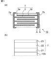
- FIG. 1 (a) shows a schematic cross-sectional view of an electronic component according to one embodiment of the present invention
- FIG. 1 (b) shows a schematic cross-sectional view of the external electrode 7b in the electronic component represented by FIG.
- the schematic cross-sectional view is shown.
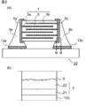
- FIG. 2A shows a schematic cross-sectional view of the mounting structure according to one embodiment of the present invention
- FIG. 2B shows B- of the external electrode 7b'in the mounting structure represented by FIG. 2A.
- a schematic cross-sectional view along the B plane is shown.
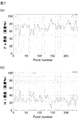
- a graph showing fluctuations in Fe concentration is shown with Point number on the horizontal axis and Fe concentration on the vertical axis.
- the cross-sectional view of the layer containing the Ni—Fe based alloy contained in the external electrode obtained in Example 2 is shown.
- FIG. 5 (a) shows a graph showing fluctuations in Fe concentration in the layer having a Ni—Fe-based alloy contained in the external electrode obtained in Example 1
- FIG. 5 (b) shows a graph showing fluctuations in Ni concentration.
- FIG. 6A shows a graph showing fluctuations in Fe concentration in the layer having a Ni—Fe-based alloy contained in the external electrode obtained in Example 2
- FIG. 6B shows a graph showing fluctuations in Ni concentration.
- FIG. 7A shows a graph showing fluctuations in Fe concentration in the layer having a Ni—Fe-based alloy contained in the external electrode obtained in Example 3
- FIG. 7B shows a graph showing fluctuations in Ni concentration. Is shown.
- FIG. 9A shows a graph showing fluctuations in Fe concentration in the layer having a Ni—Fe-based alloy contained in the external electrode obtained in Test Example 1
- FIG. 9B shows a graph showing fluctuations in Ni concentration. Is shown.
- FIG. 10A shows a graph showing fluctuations in Fe concentration in the layer having a Ni—Fe-based alloy contained in the external electrode obtained in Test Example 2
- FIG. 10B shows a graph showing fluctuations in Ni concentration. Is shown.
- FIG. 11 (a) shows a graph showing the fluctuation of the Fe concentration in the layer having the Ni—Fe-based alloy contained in the external electrode obtained in Test Example 3, and FIG.
- FIG. 11 (b) shows the graph showing the fluctuation of the Ni concentration. Is shown.
- FIG. 12 (a) shows a graph showing fluctuations in Fe concentration in the layer having a Ni—Fe-based alloy contained in the external electrode obtained in Example 4, and
- FIG. 12 (b) shows a graph showing fluctuations in Ni concentration. Is shown.
- the graph which shows the result of the stickiness test between the electronic component and the substrate obtained in Example 3 and Comparative Examples 1 and 2 is shown.
- the evaluation results of the heat resistance test of the external electrodes obtained in Test Example 3 and Comparative Example 3 are shown.
- the evaluation result of the heat resistance test of the external electrode obtained in Example 4 is shown.
- the electronic component of this embodiment is with the parts body It is provided with an external electrode provided on the surface of the component body.
- the external electrode comprises a layer having an alloy of at least one first metal and at least one second metal.
- the at least one first metal is selected from the group consisting of Group 9 to Group 11 metals in the Periodic Table of the Elements.
- the at least one second metal has a higher melting point than the at least one first metal.
- the concentration of the at least one second metal changes continuously in the thickness direction of the external electrode, and at least one portion where the concentration of the metal increases and a portion where the concentration of the metal decreases, respectively.
- the "layer having an alloy” means "a layer having an alloy of at least one first metal and at least one second metal" unless otherwise specified.
- the component body is not particularly limited as long as an external electrode can be provided on the surface thereof, but for example, the body of the electronic component that can be used as a capacitor, an inductor, a resistor, an LC composite component, or the like is used. Can be mentioned.
- the above-mentioned component body is not particularly limited, and can be configured by using a commonly used method.
- the material of the above-mentioned component body is not particularly limited, and a commonly used material can be used.
- the material include ceramics, resins, metals, composite materials thereof, and the like, and specific examples thereof include ceramics.
- the electronic component of this embodiment can be, for example, the multilayer ceramic capacitor 10 shown in FIG. 1 (a).
- the monolithic ceramic capacitor 10 includes a component body 1 and an external electrode 7 provided on the surface of the component body.
- the component body 1 has an internal electrode 3 (3a, 3b in FIG. 1A) and a dielectric portion (dielectric layer) 5.
- the drawings include some schematic ones and may not reflect the actual dimensions and ratios.
- the number of the external electrodes is not particularly limited, and a plurality of external electrodes can be provided.
- 7a and 7b are provided as the external electrodes 7.
- the external electrode 7 has a layer having an alloy (for example, a layer having a Ni—Fe based alloy) 22.
- the external electrode 7 may further have a layer 23 in contact with the layer 22 having an alloy. If layer 23 is present, layer 23 can be the outermost layer of the external electrode. Examples of the layer 23 include a layer containing Sn (Sn plating layer) and the like. In this case, the bondability with the solder can be improved (in other words, the "solder wettability" can be improved) when mounting.
- the external electrode may further have a layer 21 in contact with the layer 22 having an alloy.
- the layer 21 may come into direct contact with the component body 1 (typically 5).
- the layer 21 include a layer containing Ag (more specifically, an Ag paste layer) and the like. In this case, the contact between the component body 1 and the external electrode 7 can be improved.
- a layer containing Ag is provided as the layer 21, for example, by having the layer 22 having an alloy, solder erosion from the layer containing Ag can be prevented. In this case, the connection between the component body and the layer containing Ag is good, and the connection reliability as an electronic component may also be good.
- the thickness of the external electrode is not particularly limited, but may be, for example, in the range of 1 to 500 ⁇ m, in the range of 3 to 300 ⁇ m, or in the range of 5 to 20 ⁇ m.
- the at least one first metal is selected from a group consisting of the metals of Groups 9 to 11 of the Periodic Table of the Elements, and the at least one second metal has a higher melting point than the at least one first metal.
- the melting point can be obtained as the temperature of the endothermic peak in the differential scanning calorimetry (DSC). Specifically, in DSC, for example, it can be measured as the peak top temperature at the crystal melting peak observed when the temperature is raised at 3 ° C./min under a nitrogen atmosphere. When multiple endothermic peaks are observed, the lowest temperature is taken as the melting point.
- DSC differential scanning calorimetry
- the melting point of "at least one first metal” indicates the melting point of the alloy containing the two or more kinds of metals.
- the melting point of "at least one second metal” indicates the melting point of the alloy containing the two or more kinds of metals.
- At least one first metal is selected from the group consisting of, for example, Ni, Co, Ag and Cu.
- At least one second metal is selected from the group consisting of, for example, W, Re, Os, Mo, Nb, Ir, Ru, Rh, Cr, Pt, Ti, Lu, Pd, Fe, and Co.
- At least one first metal is selected from the group consisting of Ni, Co, Ag and Cu
- at least one second metal is W, Re, Os, Mo, Nb, Ir, Ru, Rh, It is selected from the group consisting of Cr, Pt, Ti, Lu, Pd, Fe, and Co.
- the at least one first metal is specifically Ni, Co, Ag, or Cu, and more specifically Ni.
- the at least one second metal is specifically W, Re, Os, Mo, Nb, Ir, Ru, Rh, Cr, Pt, Ti, Lu, Pd, Fe, or Co, more specifically. Is Fe, Pd or W.
- At least one first metal is Ni and at least one second metal is selected from the group consisting of Fe, Pd, and W.
- at least one first metal is Ni and at least one second metal is Fe, Pd, or W.
- the alloy contained in the layer having the alloy is a Ni—Fe based alloy, a Ni—Pd based alloy, or a Ni—W alloy, and specifically, a Ni—Fe based alloy.
- the concentration of at least one second metal changes continuously in the thickness direction of the external electrode, and the portion where the concentration of at least one second metal increases and the portion where the concentration decreases, respectively.
- the layer having the alloy can be formed in a direction away from the surface of the component body.
- concentration of at least one second metal changes continuously means that the metal contains a plurality of metals (that is, when there are a plurality of second metals contained in a layer having an alloy). , The concentration of one of the plurality of metals may be continuously changed.
- the concentration of at least one second metal increases means that when the metal contains a plurality of metals, the concentration of one metal among the plurality of metals may increase, and "the concentration of at least one second metal increases”.
- the concentration of the metal decreases means that when the metal contains a plurality of metals, the concentration of one of the plurality of metals may be reduced.
- the external electrode includes a layer having a Ni—Fe based alloy.
- the Fe concentration continuously changes in the thickness direction of the external electrode, and there is at least one portion where the Fe concentration increases and one portion where the Fe concentration decreases.
- a layer having a Ni—Fe-based alloy The layer having the Ni—Fe based alloy can be formed in a direction away from the surface of the component body.
- the electronic component when the external electrode contains a layer having a Ni—Fe based alloy, the electronic component is With the parts body It is provided with an external electrode provided on the surface of the component body.
- the external electrode may include a layer having a Ni—Fe based alloy.
- the Fe concentration continuously changes in the thickness direction of the external electrode, and there is at least one portion where the Fe concentration increases and one portion where the Fe concentration decreases.
- the alloy in the layer having the alloy, may contain a metal other than the first metal and the second metal as long as the effect of the present invention is not impaired.
- the alloy when the alloy is an alloy containing Ni and Fe (sometimes referred to as "Ni-Fe-based alloy"), it contains metal atoms other than Ni and Fe as long as the effects of the present invention are not impaired. You may be.
- the content of metal atoms other than the first metal and the second metal in the layer having the alloy is not particularly limited, but is, for example, 10% by mass or less, specifically, 1% by mass, based on the total mass of the alloy. It is as follows.
- the lower limit of the content of metal atoms other than the first metal and the second metal may be 0% by mass with respect to the total mass of the alloy.
- the content of metal atoms other than Ni and Fe in the Ni—Fe based alloy is not particularly limited, but with respect to the total mass of the Ni—Fe based alloy.
- it is 10% by mass or less, specifically, 1% by mass or less.
- the lower limit of the content of metal atoms other than Ni and Fe may be 0% by mass with respect to the total mass of the Ni—Fe-based alloy.
- the alloy eg, Ni—Fe based alloy
- the alloy is free of metal atoms other than at least one first metal and at least one second metal (eg Ni and Fe), except for unavoidable impurities. ..
- an external electrode having good heat resistance can be provided, and further, a better bonding strength is provided between the electronic component including the external electrode and the substrate. obtain.
- the Ni—Fe alloy contains atoms other than Ni and Fe, specifically Sn, Ag, Cu, Co, Ti, Ba, Mn, Ca, Sr, Na, K, Mg, Al and the like. May contain metal atoms of.
- the layer having an alloy is a layer containing at least one first metal and at least one second metal, and is a first metal other than the first metal and the second metal as long as the effects of the present invention are not impaired. It may contain three components.
- the layer having the above alloy is a "layer having a Ni-Fe-based alloy”
- the layer is a layer containing a "Ni-Fe-based alloy”
- Ni is within a range that does not interfere with the effects of the present invention. It may contain a third component other than the ⁇ Fe-based alloy.
- Examples of the third component include S, C, O, Cl, P, B, and N atoms, which are effective in reducing the stress of the film.
- the content of the atom, which is the third component, may be contained in the range of, for example, 0 to 10% by mass, specifically in the range of 0 to 1% by mass, with respect to the total mass of the layer having the alloy. obtain.
- the alloy for example, Ni—Fe based alloy
- the alloy may contain other trace substances, for example, trace elements that can be unavoidably mixed.
- the electronic component of this embodiment can be used in a mounting structure by mounting it on a substrate using solder.
- a mounting structure as shown in FIG. 2A can be mentioned.
- the mounting structure 20 has an electronic component and a solder joint 9.
- the electronic component includes a component body 1 and an external electrode 7'provided on the surface of the component body.
- the component body 1 has an internal electrode 3 and a dielectric portion (dielectric layer) 5.
- the number of the external electrodes is not particularly limited, and a plurality of external electrodes can be provided.
- 7a'and 7b' are provided as the external electrodes 7'.
- solder joints 9 can be provided as 9a and 9b.
- the solder joint portion 9 joins the substrate 11 and electronic components, and specifically, directly joins the electrode portion 13 provided on the surface of the substrate 11.
- the number of electrode portions 13 is appropriately selected according to the number of electronic components, but can be typically two (13a, 13b).
- the external electrode 7'in the mounting structure of the present embodiment for example, the one represented by FIG. 2B can be mentioned.
- the external electrode has a layer having an alloy (for example, a layer having a Ni—Fe based alloy) 22'.
- the external electrode 7' may further have a layer 21 in contact with the layer 22' having an alloy.
- the layer 21 may come into direct contact with the component body 1 (typically 5).
- the layer 21 include a layer containing Ag (Ag paste layer) and the like. In this case, the contact between the component body and the external electrode can be good.
- the mounting structure of this embodiment has a solder joint 9 in contact with a layer 22'having an alloy.
- the interface between the layer having an alloy (for example, the layer having a Ni—Fe-based metal) 22'and the solder joint portion 9 is formed. It may have an uneven state. It is formed due to the increasing and decreasing concentrations of at least one second metal (eg, Fe) in the layer having the alloy.
- the present invention is not limited to any theory, but it is considered that at least one low-concentration portion of the second metal is likely to be contained in the solder joint portion 9. In the present embodiment, it is considered that having such an interface shape strengthens the bonding strength between the electronic component and the substrate.
- the concentration of at least one second metal in the layer having the alloy was measured using a scanning electron microscope (FE-SEM / EDX) (manufactured by Hitachi High-Technologies Corporation, FE-SEM: SU8230 / EDX: 5060FQ). The value. Specifically, it is performed as follows. The layer having the alloy is cut in the thickness direction of the external electrode and the cross section is polished. Then, using FE-SEM / EDX, the acceleration voltage is set to 3 kV, and the weight of the metal element contained in the layer having the system alloy is measured.
- the concentration of at least one second metal means the ratio of the weight of the second metal to the total weight of the first metal and the second metal contained in the external electrode. For example, when the alloy is a Ni—Fe based alloy, “Fe concentration” means the ratio of the weight of the Fe element to the total weight of the Ni element and the Fe element.
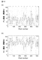
- the concentration of at least one second metal is measured as follows. A plurality of points are evenly provided per unit thickness (specifically, 1.0 ⁇ m), and at least sequentially from the points provided on the side closer to the outermost surface of the external electrode (that is, when the horizontal axis is 0). The concentration of one second metal is measured. Based on the measurement results, for example, a graph as shown in FIG. 3 can be formed.
- FIG. 3 shows the measurement of Fe concentration when a Ni—Fe based alloy is used as the alloy.
- the left side when the horizontal axis is 0
- the right side shows the side close to the component body.
- the horizontal axis is “Point number”, which corresponds to the order of the points at which the Fe concentration was measured as described above.
- the vertical axis is the Fe concentration.
- the Fe concentration is a value obtained by using FE-SEM / EDX as described above.
- the Fe concentration continuously changes between the minimum value and the maximum value.
- “continuously” means that the measurement points exist without being discrete.
- the Fe concentration at 100 points or more (specifically, 130 points or more, 236 points in the example shown in FIG. 3) per unit thickness (per 1.0 ⁇ m) is measured, and the Fe concentration at a certain measurement point and its The amount of change from the Fe concentration at the adjacent measurement point can be 30% or less.
- the region represented by ⁇ is a portion where the Fe concentration value continuously increases from the minimum value to the maximum value (“the portion where the Fe concentration increases”), and is represented by ⁇ .
- the region to be formed is a portion where the Fe concentration continuously decreases from the maximum value to the minimum value (“the portion where the Fe concentration decreases”).
- the layer having the alloy there is at least one portion in which the concentration of at least one second metal increases and one portion decreases in the thickness direction of the external electrode.
- the layer having an alloy is a layer having a Ni—Fe alloy
- At least one portion where the concentration of the second metal increases can be present in the layer having the alloy in the thickness direction of the external electrode, for example, 1 to 100 per 1 ⁇ m, specifically, 1 to 100 per 1 ⁇ m.
- the alloy is a Ni—Fe based alloy
- 1 to 100 portions where the Fe concentration increases exist in the layer having the Ni—Fe based alloy in the thickness direction of the external electrode for example, per 1 ⁇ m.
- Obtain, specifically, 1 to 70 may be present per 1 ⁇ m, and more specifically, 10 to 50 may be present per 1 ⁇ m.
- At least one portion where the concentration of the second metal is reduced may be present in the layer having the alloy in the thickness direction of the external electrode, for example, 1 to 100 per 1 ⁇ m, specifically, 1 to 100 per 1 ⁇ m.
- the alloy is a Ni—Fe based alloy
- there are 1 to 100 portions in the layer having the Ni—Fe based alloy in the thickness direction of the external electrode for example, per 1 ⁇ m.
- Obtain, specifically, 1 to 70 may be present per 1 ⁇ m, and more specifically, 10 to 50 may be present per 1 ⁇ m.
- the external electrode By having a layer having an alloy as described above (for example, a layer having a Ni—Fe alloy), the external electrode exhibits good heat resistance. As a result, when the electronic component of the present embodiment is mounted, solder erosion of the layer having the alloy can be suppressed. Further, by having the layer having the alloy as described above, when the electronic component of this embodiment is mounted on the substrate, the bonding strength between the electronic component and the substrate can be improved.
- a plurality of layers having different concentrations of at least one second metal laminated in the thickness direction of the external electrode are formed.
- the presence of a plurality of layers having different concentrations of at least one second metal constitutes an increasing portion and a decreasing portion of the concentration of at least one second metal.
- the concentration of at least one second metal is different means that when the metal contains a plurality of metals, the concentration of one metal among the plurality of metals may be different.
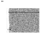
- FIG. 4 is a cross-sectional photograph of a layer having a Ni—Fe based alloy, which is cut along the thickness direction of the external electrode.
- the right side is the surface close to the component body.
- FIG. 4 above is an elemental mapping of a cross section of a layer having a Ni—Fe based alloy using FE-SEM / EDX.
- the color in the drawing is displayed lightly, and when the Fe concentration is low, the color in the drawing is displayed dark.
- the above-mentioned "there are a plurality of layers having different Fe concentrations” means that, as shown in FIG. 4, layers having different levels of Fe concentration are continuously present in a layered state in a direction substantially parallel to the surface of the component body. Means.
- the concentration of at least one second metal is particularly high. It is considered that the layer has better heat resistance, and is particularly advantageous in terms of heat resistance. Further, in the layer having the above alloy (specifically, the layer having a Ni—Fe alloy), the concentration of at least one second metal (specifically, the Fe concentration) is continuously changed. Therefore, even if cracks occur in the layer, the growth of cracks can be suppressed because the physical properties differ between the horizontal direction and the vertical direction with respect to the thickness.
- the layer having the alloy there are a plurality of regions in which the concentration of at least one second metal is different.
- the alloy is a Ni—Fe based alloy
- the presence of a plurality of regions having different concentrations of at least one second metal constitutes an increasing portion and a decreasing portion of the concentration of at least one second metal.
- FIG. 8 is a cross-sectional photograph of a layer having a Ni—Fe-based alloy, which is cut along the thickness direction of the external electrode.
- the right side is the surface of the external electrode on the component body side.
- FIG. 8 is an elemental mapping of the cross section of the layer having the Ni—Fe based alloy using FE-SEM / EDX.
- the color in the drawing is displayed lightly, and when the Fe concentration is low, the color in the drawing is displayed dark.
- the above-mentioned "there are a plurality of regions having different Fe concentrations" means that, as shown in FIG. 8, a region having a high Fe concentration and a region having a low Fe concentration coexist regardless of the direction. ..
- the heat resistance of the external electrode is improved, and in particular, the electrons of the present embodiment are obtained.
- the adhesive strength between the component and the substrate can be good. This is because a region having a high concentration (for example, Fe concentration) of at least one second metal exists in a mixture, and therefore, when a solder joint portion is provided, the solder joint portion and the external electrode are used. Concavo-convex regions are likely to be formed at the interface.
- Regular having different concentrations of at least one second metal means that when the metal contains a plurality of metals (that is, when a layer having an alloy contains a plurality of second metals), among the plurality of metals. It suffices if the concentration of one metal is different.
- the layer having the alloy preferably, there is at least one portion in which the concentration of at least one first metal increases and one portion decreases in the thickness direction of the external electrode.
- the alloy is a Ni—Fe alloy
- the layer having the Ni—Fe alloy preferably, at least one portion of the Ni concentration increases and one portion decreases in the thickness direction of the external electrode.
- the increasing portion and the decreasing portion of the increasing portion and the decreasing portion of the concentration of at least one first metal are the increasing portions at the concentration of at least one second metal, respectively. And is synonymous with the decreasing part.
- the concentration of the at least one first metal changes continuously in the thickness direction of the external electrode.
- the alloy is a Ni—Fe based alloy
- the Ni concentration in the layer having the Ni—Fe based alloy continuously changes in the thickness direction of the external electrode.
- the layer having the alloy there may be 1 to 100 portions of at least one first metal in which the concentration increases, for example, in the thickness direction of the external electrode, for example, 1 to 100 per ⁇ m.
- the alloy is a Ni—Fe based alloy
- 1 to 70 may be present per 1 ⁇ m
- 10 to 50 may be present per 1 ⁇ m.
- the layer having the alloy there may be 1 to 100 portions of at least one first metal in which the concentration is reduced, for example, 1 to 100 per ⁇ m in the thickness direction of the external electrode, and specifically, 1 to 100 portions per 1 ⁇ m.
- the alloy is a Ni—Fe based alloy
- the ratio of at least one second metal contained in the layer is preferably in the range of 1 to 99% by mass, for example, in the range of 15 to 99% by mass and 50 to 99% by mass. Or in the range of 65 to 90% by mass.
- the ratio may be in the range of 15 to 80% by mass.
- the alloy is a Ni—Fe based alloy
- the ratio of Fe contained in the layer is preferably in the range of 1 to 99% by mass, and 15 to 99. It may be in the range of 50 to 99% by mass, 65 to 90% by mass, or 70 to 90% by mass.
- the ratio of at least one second metal can be determined using FE-SEM / EDX. Specifically, it is performed as follows. The layer having the alloy is cut in the thickness direction of the external electrode and the cross section is polished. Then, using FE-SEM / EDX, the acceleration voltage is set to 3 kV, and the weight of the metal element contained in the layer having the alloy is measured. The analysis can be performed, for example, by providing a region having a length of 2 ⁇ m and a width of 2 ⁇ m and analyzing the metal elements contained in the region.
- the concentration of at least one second metal is at least one with respect to the total weight of at least one first metal and at least one second metal (ie, the total weight of the first and second metals contained in the external electrode). It means the weight ratio of two second metals.
- “Fe concentration” means the ratio of the weight of the Fe element to the total weight of the Ni element and the Fe element.
- ratio of at least one second metal means the ratio of the total amount of the second metal contained in the layer having the alloy.
- the thickness of the layer having the alloy is not particularly limited, but may be in the range of 1 to 30 ⁇ m or 1 to 15 ⁇ m, for example. It may be in the range of 1 to 8 ⁇ m.
- the layer having an alloy can have good heat resistance, and further, when the electronic component and the substrate of this embodiment are joined by using solder, the electronic component and the substrate are joined. Adhesion with and can be good.
- the external electrode may have other layers in addition to the layer having the alloy. That is, the external electrode may have a plurality of layers.
- the other layer and the layer having an alloy are laminated in the thickness direction of the external electrode.
- the substance constituting the other layer for example, at least one selected from Ag, Cu, Sn, Au, Ti, Cr, Mo, Ta, Zr, Nb, W, Al, Co, Ni, Fe, and Pd. Two metals or alloys thereof can be mentioned.
- the external electrode may have a plurality of layers having an alloy. Specifically, the external electrode may have a plurality of layers having a Ni—Fe-based alloy.
- the method for forming the external electrode is not particularly limited as long as the external electrode can be appropriately bonded to the component body, but for example, a method including application of a conductive paste, a plating method (for example, an electrolytic plating method, a non-electrolytic method). Plating method), sputtering, vapor deposition, etc. can be mentioned.
- the above method can be performed using a commonly used method.
- the layer formed directly on the surface of the component body is formed by applying a conductive paste
- the layer formed on the layer provided by applying the conductive paste is a plating method, specifically, an electrolytic plating method.
- the layer having the above alloy (for example, the layer having a Ni—Fe based alloy) can be formed by a plating method, and specifically, can be formed by an electrolytic plating method.
- Examples of the electrolytic plating method include a barrel plating method and a rack plating method.
- the voltage value applied to the object to be plated is varied.
- the barrel plating method may be suitable for forming a layer having a Ni—Fe-based alloy in which a plurality of layers having different Fe concentrations laminated in the thickness direction of the external electrode are present, and the rack plating method is Fe. It may be suitable for forming a layer having a Ni—Fe based alloy having a plurality of regions having different concentrations.
- the electronic component of this embodiment can be mounted on a board (mounting board) and become a mounting structure.
- the mounting structure of this embodiment is A mounting structure in which electronic components are mounted on a board.
- the electronic component is With the parts body It is provided with an external electrode provided on the surface of the component body.
- the external electrode comprises a layer having an alloy of at least one first metal and said at least one second metal.
- the at least one first metal is selected from the group consisting of Group 9 to Group 11 metals in the Periodic Table of the Elements.
- the at least one second metal has a higher melting point than the at least one first metal.
- the concentration of the at least one second metal changes continuously in the thickness direction of the external electrode, and at least one portion where the concentration of the metal increases and a portion where the concentration of the metal decreases, respectively.
- the external electrode is joined to the electrode portion formed on the substrate by a solder joint portion.
- the mounting structure is Electronic components are mounted on the board
- the electronic component is With the parts body It is provided with an external electrode provided on the surface of the component body.
- the external electrode includes a layer having a Ni—Fe based alloy.
- the Fe concentration continuously changes in the thickness direction of the external electrode, and there is at least one portion where the Fe concentration increases and at least one portion where the Fe concentration decreases.
- the external electrode is joined to the electrode portion formed on the substrate by a solder joint portion.
- the substrate is not particularly limited, and a commonly used substrate can be used.
- the substrate include alumina, epoxy glass, glass, Si wafer, ferrite wafer and the like.
- the electrode portion provided on the surface of the substrate is not particularly limited, and a commonly used one can be used.
- the electrode portion may be formed of, for example, a conductive substance such as Ni, Cu, Ag, Sn, Au, Pd, and optionally a preflux or the like.
- solder joint portion between the external electrode and the electrode portion.
- the solder joint may consist substantially of solder and may further contain at least one metal atom derived from an external electrode included in the electronic component of this embodiment.
- the electronic component of the first embodiment is used.
- the external electrode has a layer having an alloy (for example, a layer having a Ni—Fe based alloy). By having the layer having the alloy, it is possible to suppress the solder eating of the layer having the alloy even when the mounting structure of this embodiment is used for a long period of time and / or in a high temperature environment.
- the external electrode when the external electrode includes a layer having an alloy (for example, a layer having a Ni—Fe-based alloy) and a layer in direct contact with the component body (for example, a layer containing Ag), It is also possible to prevent solder from being eaten from the layer containing Ag. As a result, the connection reliability in the mounting structure can be improved.
- an alloy for example, a layer having a Ni—Fe-based alloy
- a layer in direct contact with the component body for example, a layer containing Ag
- a layer having an alloy of an external electrode for example, a layer having a Ni—Fe alloy
- a solder joint portion can be bonded.
- an uneven region may exist at the interface between the layer having the alloy of the external electrode and the solder joint portion. It is considered that this is because a part of the layer having the alloy may be included as a part of the solder joint part at the time of forming the solder joint part.
- the solder joint can be formed by a general method, but for example, it can be formed by reflowing using a solder paste.
- the solder is not particularly limited, and commonly used solder can be used.
- the solder include Sn—Ag alloy, Sn—Ag—Cu alloy (SAC), Sn—Zn—Bi alloy, Sn—Cu alloy, Sn—Ag-In—Bi alloy, Sn—Zn.
- SAC Sn—Ag—Cu alloy
- Sn—Ag-In—Bi alloy Sn—Zn.
- -Al-based alloys, Sn—Sb-based alloys, Sn—Pb-based alloys and the like can be used.
- the external electrode for example, the external electrode included in the electronic component of the first embodiment
- the alloy derived from the metal atom constituting the solder joint portion (the present invention).
- intermetallic compounds exist in the vicinity of the interface between the external electrode and the solder joint portion. Due to the presence of such an intermetallic compound, the electronic component and the substrate, specifically, the external electrode and the electrode portion can be more firmly bonded.
- alloys containing Sn as solder specifically, Sn—Ag alloys, Sn—Ag—Cu alloys, Sn—Zn—Bi alloys, Sn—Cu alloys, Sn—Ag-In—Bi alloys. alloy, Sn-Zn-Al-based alloy, Sn-Sb-based alloy, using a Sn-Pb alloy or the like, when containing Fe in the layer having the alloy of the external electrodes, as an intermetallic compound, there are FeSn 2 alloy ..
- FeSn 2 alloy is present, resulting to more effectively suppress the diffusion of metal atoms into the solder joints from the external electrode, the electronic component and the substrate, specifically, more robust and the external electrode and the electrode portion Can be joined to.
- alloys containing Sn as solder specifically, Sn—Ag alloys, Sn—Ag—Cu alloys, Sn—Zn—Bi alloys, Sn—Cu alloys, Sn—Ag-In—Bi alloys.
- Sn—Zn—Al alloy, Sn—Sb alloy, Sn—Pb alloy, etc. is used and Ni is contained in the layer having the alloy of the external electrode, the Ni 3 Sn 4 alloy is used as the intermetallic compound.
- the Ni 3 Sn 4 alloy Due to the presence of the Ni 3 Sn 4 alloy, the diffusion of metal atoms from the external electrode to the solder joint can be suppressed more effectively, and the electronic component and the substrate, specifically, the external electrode and the electrode portion can be separated from each other. Can be joined more firmly.
- alloys containing Sn as solder specifically, Sn—Ag alloys, Sn—Ag—Cu alloys, Sn—Zn—Bi alloys, Sn—Cu alloys, Sn—Ag-In—Bi alloys. alloy, Sn-Zn-Al-based alloy, Sn-Sb-based alloy, using a Sn-Pb alloy or the like, if the layer having the alloy of the external electrodes containing Fe and Ni, as an intermetallic compound, FeSn 2 alloy and There are Ni 3 Sn 4 series alloys. The presence of the FeSn 2 alloy and the Ni 3 Sn 4 alloy can more effectively suppress the diffusion of metal atoms from the external electrode to the solder joint, and electronic components and substrates, specifically the external electrode. And the electrode portion can be joined more firmly.
- (Cu, Ni) 6 Sn 5 means that the ratio of Cu and Ni and Sn exists in a ratio of 6: 5.
- the thickness of the layer in which the intermetallic compound is present is not particularly limited, but may be in the range of 0.01 to 20 ⁇ m, for example.
- the thickness of the layers present in the FeSn 2 alloy is not particularly limited, for example, can range from 0.01 ⁇ 20 [mu] m.
- Example 1 The chip-shaped ceramic laminate was immersed in the paste in which Ag powder and glass were mixed, and then pulled up to attach the paste. Then, it was fired at 760 ° C. to form a composite layer containing Ag and glass on the surface of the ceramic laminate.
- iron salt iron sulphate heptahydrate: 28 g / L
- nickel salt nickel sulphate hexahydrate: 250 g / L
- nickel chloride hexahydrate 40 g / L
- ⁇ Method (A1-1) A layer having a Ni—Fe based alloy was formed by using a barrel plating method.
- the object to be processed and the metal for ensuring continuity are put into a barrel-type plating apparatus, and the voltage value is 5 to 15 V for 60 minutes at 10 A (average current density 0.29 A / dm 2 ). It was processed by varying within the range of.
- the Sn plating layer was formed by the method (A1-2) using a plating solution containing a Sn salt, a complexing agent, and an additive. ⁇ Method (A1-2) The Sn layer was formed using the barrel plating method. Specifically, the object to be treated and the metal for ensuring continuity were put into a barrel-type plating apparatus and processed at 6 A for 75 minutes. As described above, an electronic component having an external electrode was produced.
- Example 2 In the formation of the plating layer of the Ni—Fe alloy, the same procedure as in Example 1 was carried out except that the iron salt concentration was changed to iron sulfate heptahydrate: 56 g / L to prepare an electronic component having an external electrode. ..
- Example 3 In the formation of the plating layer of the Ni—Fe based alloy, the same procedure as in Example 1 was carried out except that the iron salt concentration was changed to iron sulfate heptahydrate: 97 g / L to prepare an electronic component having an external electrode. ..
- Example 4 In the formation of the plating layer of the Ni—Fe based alloy, the same procedure as in Example 1 was carried out except that the iron salt concentration was changed to iron sulfate heptahydrate: 117 g / L to prepare an electronic component having an external electrode. ..
- ⁇ Method (A4-1) Using the rack plating method, processing was performed at 1.3 A (average current density 4.0 A / dm 2 ) for 4 minutes and 20 seconds with the voltage value varied in the range of 2.0 to 2.6 V.
- the Sn plating layer was formed by the method (A4-2) using a plating solution containing a Sn salt, a complexing agent, and an additive.
- ⁇ Method (A4-2) Using the rack plating method, processing was performed at 0.085 A (average current density 0.25 A / dm 2 ) for 40 minutes. As described above, a part having a layer having a Ni—Fe alloy and a Sn layer was produced.
- Test Example 2 In the formation of the plating layer of the Ni—Fe alloy, the same procedure as in Test Example 1 was carried out except that the iron salt concentration was changed to iron sulfate heptahydrate: 56 g / L, and the layer having the Ni—Fe alloy and the layer having the Ni—Fe alloy were formed. A part having a Sn layer was produced.
- Test Example 3 In the formation of the plating layer of the Ni—Fe alloy, the same procedure as in Test Example 1 was carried out except that the iron salt concentration was changed to iron sulfate heptahydrate: 97 g / L, and the layer having the Ni—Fe alloy and the layer having the Ni—Fe alloy were formed. A part having a Sn layer was produced.
- FIGS. 5 (a), 5 (b), 6 (a), 6 (b), and 7 show the analysis results of the Fe ratio and the Ni ratio of Test Examples 1 to 3, respectively, in FIGS. 9 (a) and 9 (b).
- the number of portions where the Fe concentration increases was determined from the analysis results.
- the table below shows the number of parts where the Fe concentration increases. The number of "parts where the Fe concentration increases" is a value obtained by counting those where the Fe concentration has decreased and then increased.
- ⁇ Ratio of Fe in the layer having Ni—Fe alloy The content of the Fe element with respect to the total mass of the Fe element and the Ni element contained in the layer having the Ni—Fe based alloy was determined.
- an analysis region having a length of 2 ⁇ m or more and a width of 2 ⁇ m or more is provided in the cross section of the layer having a Ni—Fe alloy, and the masses of Fe element and Ni element contained in the region are measured using EDX. It is calculated based on the measured value.
- the conditions of EDX are the same as the above-mentioned cross-section analysis method.
- the table below shows the analysis results of the cross section of the layer having the Ni—Fe based alloy obtained in Examples 1 to 4 and Test Examples 1 to 3.
- FIG. 4 shows a cross-sectional view (magnification: 50,000 times) of the layer having the Ni—Fe based alloy obtained in Example 2
- FIG. 8 shows a cross section of the layer having the Ni—Fe based alloy obtained in Test Example 3.
- the figures (magnification: 50,000 times) are shown respectively.
- 6 (a) and 6 (b) are the results of measuring the Fe concentration and the Ni concentration by providing points along the horizontal lines shown in FIG. 4, and FIGS. 11 (a) and 11 (b) are shown. , The result of measuring the Fe concentration and the Ni concentration by providing points along the horizontal line shown in FIG. In FIGS.
- a Sn plating layer was formed by the method (B1-2) using a plating solution containing a Sn salt, a complexing agent, and an additive.
- the Sn layer was formed using the barrel plating method. Specifically, the object to be treated and the metal for ensuring continuity were put into a barrel-type plating apparatus and processed at 6 A for 75 minutes. As described above, an electronic component having an external electrode was produced.
- a Ni layer was formed using 2).
- a Sn plating layer was formed by the method (B2-3) using a plating solution containing a Sn salt, a complexing agent, and an additive.
- the Sn layer was formed using the barrel plating method. Specifically, the object to be treated and the metal for ensuring continuity were put into a barrel-type plating apparatus and processed at 6 A for 75 minutes. As described above, an electronic component having an external electrode was produced.
- Example 3 The electronic components obtained in Example 3 and Comparative Examples 1 and 2 were mounted on a substrate, and the adhesiveness between the electronic components and the substrate was measured.
- the method for evaluating the stickiness is as follows.
- Example 3 and Comparative Examples 1 and 2 were reflow-mounted on a printed circuit board using SAC, and then the adhesion strength was measured by a lateral pressing test.
- the conditions for the sideways push test are as follows. ⁇ Equipment Adhesion strength evaluation machine (Bond tester Dage4000; made by Dage) Module: BS 5kg Tool: SHR-187-2000 (1mm width) ⁇ Evaluation condition module: BS5kg Tool: SHR-187-2000 (1mm width) Descent speed ( ⁇ m / s): 100 Share speed ( ⁇ m / s): 100 Share height ( ⁇ m): 100 Destruction recognition point: 30% n number: 10
- Example 4 The electronic components obtained in Example 4, Test Example 3, and Comparative Example 3 were allowed to stand at 150 ° C. for 1000 hours or at 200 ° C. for 1000 hours, respectively. Then, elemental mapping of the cross section was performed under the following conditions.
- -Analytical instrument Scanning electron microscope (FE-SEM / EDX) Made by Hitachi High-Technologies Corporation FE-SEM: SU8230 / EDX: 5060FQ Magnification: 10000 times
- FIG. 14 and 15 show the results of element mapping. "Initial” is a cross-sectional view before the heat resistance test.
- FIG. 14 shows the results of Test Example 3 and Comparative Example 3, specifically, the results at the initial stage, after 1000 hours at 150 ° C., and after 1000 hours at 200 ° C., respectively.
- FIG. 15 shows the results of Example 4, specifically, the results at the initial stage and after the lapse of 1652 hours at 200 ° C.
- a layer that appeared white was confirmed near the center of each cross-sectional view (FIG. 14). This is where the Ni—Fe based alloy exists.
- the widths of the layers that appear white in the initial cross-sectional view, the cross-sectional view after 1000 hours at 150 ° C., and the cross-sectional view after 1000 hours at 200 ° C. are defined as A1, A2, and A3.
- A1 white-looking layer
- A2 width equivalent to the initial width A1
- the layer state was maintained even after the lapse of 1000 hours at 200 ° C., although the width was slightly smaller than the initial width A1.
- a layer that appeared white was confirmed near the center of each cross-sectional view (FIG. 15). This is where the Ni—Fe based alloy exists.
- Example 4 the widths of the layers that appear white in the initial cross-sectional view and the cross-sectional view after the lapse of 1652 hours at 200 ° C. are defined as C1 and C2. It was confirmed that the layer state was maintained even after the lapse of 1652 hours at 200 ° C., although the width was slightly smaller than the initial width C1.
- Comparative Example 3 a layer that appeared white was confirmed near the center in the cross-sectional view at the initial stage and after 1000 hours at 150 ° C. (FIG. 14). This is where Ni exists.
- a white-looking layer (width B2) having a width equivalent to the white-looking layer width B1 in the initial cross-sectional view was observed.
- the layer state that appeared white could not be confirmed, and the Ni layer disappeared.
- the present invention can be used in applications that require connectivity between electronic components and substrates.
Abstract
Le composant électronique comprend un corps de composant principal et une électrode externe disposée sur la surface avers du corps de composant principal. L'électrode externe comprend une couche ayant un alliage d'au moins un premier métal et d'au moins un second métal. L'au moins un premier métal est choisi dans le groupe constitué par les métaux du groupe 9 et le groupe 11 du tableau périodique des éléments. L'au moins un second métal a un point de fusion supérieur à celui de l'au moins un premier métal. Dans la couche ayant l'alliage, il y a au moins une partie dans laquelle la concentration de l'au moins un second métal varie en continu dans la direction de l'épaisseur de l'électrode externe et la concentration du métal augmente, et il y a au moins une partie dans laquelle la concentration de l'au moins un second métal varie en continu dans la direction de l'épaisseur de l'électrode externe et la concentration du métal diminue.
Priority Applications (3)
| Application Number | Priority Date | Filing Date | Title |
|---|---|---|---|
| CN202080031542.9A CN113728406B (zh) | 2019-04-26 | 2020-04-17 | 电子部件和安装结构体 |
| JP2021516090A JP7188568B2 (ja) | 2019-04-26 | 2020-04-17 | 電子部品および実装構造体 |
| US17/510,549 US11776754B2 (en) | 2019-04-26 | 2021-10-26 | Electronic component and mounting structure |
Applications Claiming Priority (4)
| Application Number | Priority Date | Filing Date | Title |
|---|---|---|---|
| JP2019-086480 | 2019-04-26 | ||
| JP2019086480 | 2019-04-26 | ||
| JP2019-181340 | 2019-10-01 | ||
| JP2019181340 | 2019-10-01 |
Related Child Applications (1)
| Application Number | Title | Priority Date | Filing Date |
|---|---|---|---|
| US17/510,549 Continuation US11776754B2 (en) | 2019-04-26 | 2021-10-26 | Electronic component and mounting structure |
Publications (1)
| Publication Number | Publication Date |
|---|---|
| WO2020218218A1 true WO2020218218A1 (fr) | 2020-10-29 |
Family
ID=72942716
Family Applications (1)
| Application Number | Title | Priority Date | Filing Date |
|---|---|---|---|
| PCT/JP2020/016963 WO2020218218A1 (fr) | 2019-04-26 | 2020-04-17 | Composant électronique et structure de montage |
Country Status (4)
| Country | Link |
|---|---|
| US (1) | US11776754B2 (fr) |
| JP (1) | JP7188568B2 (fr) |
| CN (1) | CN113728406B (fr) |
| WO (1) | WO2020218218A1 (fr) |
Citations (4)
| Publication number | Priority date | Publication date | Assignee | Title |
|---|---|---|---|---|
| JPH04334007A (ja) * | 1991-05-09 | 1992-11-20 | Mitsubishi Materials Corp | セラミックコンデンサ |
| JP2004083955A (ja) * | 2002-08-23 | 2004-03-18 | Murata Mfg Co Ltd | セラミック電子部品のめっき方法、及びセラミック電子部品 |
| WO2013132965A1 (fr) * | 2012-03-05 | 2013-09-12 | 株式会社村田製作所 | Composant électronique |
| JP2016076582A (ja) * | 2014-10-06 | 2016-05-12 | Tdk株式会社 | セラミック電子部品 |
Family Cites Families (11)
| Publication number | Priority date | Publication date | Assignee | Title |
|---|---|---|---|---|
| JPH06196351A (ja) | 1992-12-24 | 1994-07-15 | Kyocera Corp | 積層セラミックコンデンサの製造方法 |
| JP4423707B2 (ja) * | 1999-07-22 | 2010-03-03 | Tdk株式会社 | 積層セラミック電子部品の製造方法 |
| EP1518841A1 (fr) * | 2003-09-24 | 2005-03-30 | Yageo Corporation | Composition céramique avec compensation de température pour électrodes d'argent pur, additif de frittage et élément céramique laminé en couches |
| JP4747604B2 (ja) * | 2005-02-18 | 2011-08-17 | Tdk株式会社 | セラミック電子部品 |
| EP2824681B1 (fr) * | 2012-03-05 | 2019-04-10 | Murata Manufacturing Co., Ltd. | Composant électronique et une structure de jonction entre le composant électronique et l'objet devant être joint |
| CN104144764B (zh) * | 2012-03-05 | 2016-12-14 | 株式会社村田制作所 | 接合方法、接合结构体及其制造方法 |
| JP2014229869A (ja) * | 2013-05-27 | 2014-12-08 | 株式会社村田製作所 | セラミック電子部品 |
| JP6112060B2 (ja) * | 2013-06-19 | 2017-04-12 | 株式会社村田製作所 | セラミック電子部品およびその製造方法 |
| JP2018142609A (ja) * | 2017-02-27 | 2018-09-13 | 株式会社村田製作所 | 表面実装型電子部品 |
| JP2018160596A (ja) * | 2017-03-23 | 2018-10-11 | Tdk株式会社 | 外部電極及び外部電極の製造方法 |
| US10971302B2 (en) * | 2018-06-19 | 2021-04-06 | Taiyo Yuden Co., Ltd. | Multilayer ceramic capacitor and manufacturing method of the same |
-
2020
- 2020-04-17 WO PCT/JP2020/016963 patent/WO2020218218A1/fr active Application Filing
- 2020-04-17 JP JP2021516090A patent/JP7188568B2/ja active Active
- 2020-04-17 CN CN202080031542.9A patent/CN113728406B/zh active Active
-
2021
- 2021-10-26 US US17/510,549 patent/US11776754B2/en active Active
Patent Citations (4)
| Publication number | Priority date | Publication date | Assignee | Title |
|---|---|---|---|---|
| JPH04334007A (ja) * | 1991-05-09 | 1992-11-20 | Mitsubishi Materials Corp | セラミックコンデンサ |
| JP2004083955A (ja) * | 2002-08-23 | 2004-03-18 | Murata Mfg Co Ltd | セラミック電子部品のめっき方法、及びセラミック電子部品 |
| WO2013132965A1 (fr) * | 2012-03-05 | 2013-09-12 | 株式会社村田製作所 | Composant électronique |
| JP2016076582A (ja) * | 2014-10-06 | 2016-05-12 | Tdk株式会社 | セラミック電子部品 |
Also Published As
| Publication number | Publication date |
|---|---|
| CN113728406A (zh) | 2021-11-30 |
| US20220044873A1 (en) | 2022-02-10 |
| JP7188568B2 (ja) | 2022-12-13 |
| JPWO2020218218A1 (fr) | 2020-10-29 |
| US11776754B2 (en) | 2023-10-03 |
| CN113728406B (zh) | 2023-05-23 |
Similar Documents
| Publication | Publication Date | Title |
|---|---|---|
| US10615327B2 (en) | Monolithic ceramic electronic component | |
| JP3861927B1 (ja) | 電子部品、電子部品の実装構造および電子部品の製造方法 | |
| KR100307680B1 (ko) | Sn합금도금피막을갖는전자부품 | |
| JP2007281400A (ja) | 表面実装型セラミック電子部品 | |
| US9144166B2 (en) | Electronic component | |
| WO2013132965A1 (fr) | Composant électronique | |
| JP2009141292A (ja) | 外部端子電極具備電子部品、その搭載電子用品及び外部端子電極具備電子部品の製造方法 | |
| US9320146B2 (en) | Electronic circuit module component | |
| WO2020218218A1 (fr) | Composant électronique et structure de montage | |
| EP2309830B1 (fr) | Film de placage, carte de circuit imprimé et substrat de module | |
| JP4544896B2 (ja) | 電子部品 | |
| KR100438124B1 (ko) | 세라믹 전자 부품 | |
| JP2019117899A (ja) | 積層電子部品 | |
| JP2004186602A (ja) | 電子部品 | |
| JP7088134B2 (ja) | 電子部品 | |
| JPH0656825B2 (ja) | セラミックコンデンサ | |
| KR20210010327A (ko) | 전자부품 | |
| JP2021027196A (ja) | 電子部品および実装構造体 | |
| JP2021027195A (ja) | 電子部品および実装構造体 | |
| JP2003243245A (ja) | セラミック電子部品およびその製造方法 | |
| JP2000077253A (ja) | 電子部品、チップ型セラミック電子部品、およびそれらの製造方法 | |
| WO2023037747A1 (fr) | Structure de montage | |
| US20230154685A1 (en) | Multilayer ceramic capacitor | |
| WO2013172155A1 (fr) | Film de revêtement métallique et composant électronique muni dudit film de revêtement métallique | |
| JP2003013280A (ja) | 積層型チップ部品 |
Legal Events
| Date | Code | Title | Description |
|---|---|---|---|
| 121 | Ep: the epo has been informed by wipo that ep was designated in this application |
Ref document number: 20794335 Country of ref document: EP Kind code of ref document: A1 |
|
| ENP | Entry into the national phase |
Ref document number: 2021516090 Country of ref document: JP Kind code of ref document: A |
|
| NENP | Non-entry into the national phase |
Ref country code: DE |
|
| 122 | Ep: pct application non-entry in european phase |
Ref document number: 20794335 Country of ref document: EP Kind code of ref document: A1 |