WO2020217456A1 - 透過電子顕微鏡および透過電子顕微鏡を用いた検査方法 - Google Patents
透過電子顕微鏡および透過電子顕微鏡を用いた検査方法 Download PDFInfo
- Publication number
- WO2020217456A1 WO2020217456A1 PCT/JP2019/017938 JP2019017938W WO2020217456A1 WO 2020217456 A1 WO2020217456 A1 WO 2020217456A1 JP 2019017938 W JP2019017938 W JP 2019017938W WO 2020217456 A1 WO2020217456 A1 WO 2020217456A1
- Authority
- WO
- WIPO (PCT)
- Prior art keywords
- electron beam
- electron microscope
- sample
- transmission electron
- display
- Prior art date
- Legal status (The legal status is an assumption and is not a legal conclusion. Google has not performed a legal analysis and makes no representation as to the accuracy of the status listed.)
- Ceased
Links
Images




Classifications
-
- H—ELECTRICITY
- H01—ELECTRIC ELEMENTS
- H01J—ELECTRIC DISCHARGE TUBES OR DISCHARGE LAMPS
- H01J37/00—Discharge tubes with provision for introducing objects or material to be exposed to the discharge, e.g. for the purpose of examination or processing thereof
- H01J37/26—Electron or ion microscopes; Electron or ion diffraction tubes
-
- G—PHYSICS
- G01—MEASURING; TESTING
- G01N—INVESTIGATING OR ANALYSING MATERIALS BY DETERMINING THEIR CHEMICAL OR PHYSICAL PROPERTIES
- G01N23/00—Investigating or analysing materials by the use of wave or particle radiation, e.g. X-rays or neutrons, not covered by groups G01N3/00 – G01N17/00, G01N21/00 or G01N22/00
- G01N23/20—Investigating or analysing materials by the use of wave or particle radiation, e.g. X-rays or neutrons, not covered by groups G01N3/00 – G01N17/00, G01N21/00 or G01N22/00 by using diffraction of the radiation by the materials, e.g. for investigating crystal structure; by using scattering of the radiation by the materials, e.g. for investigating non-crystalline materials; by using reflection of the radiation by the materials
-
- H—ELECTRICITY
- H01—ELECTRIC ELEMENTS
- H01J—ELECTRIC DISCHARGE TUBES OR DISCHARGE LAMPS
- H01J37/00—Discharge tubes with provision for introducing objects or material to be exposed to the discharge, e.g. for the purpose of examination or processing thereof
- H01J37/26—Electron or ion microscopes; Electron or ion diffraction tubes
- H01J37/261—Details
- H01J37/265—Controlling the tube; circuit arrangements adapted to a particular application not otherwise provided, e.g. bright-field-dark-field illumination
-
- H—ELECTRICITY
- H01—ELECTRIC ELEMENTS
- H01J—ELECTRIC DISCHARGE TUBES OR DISCHARGE LAMPS
- H01J37/00—Discharge tubes with provision for introducing objects or material to be exposed to the discharge, e.g. for the purpose of examination or processing thereof
- H01J37/26—Electron or ion microscopes; Electron or ion diffraction tubes
- H01J37/295—Electron or ion diffraction tubes
-
- G—PHYSICS
- G01—MEASURING; TESTING
- G01N—INVESTIGATING OR ANALYSING MATERIALS BY DETERMINING THEIR CHEMICAL OR PHYSICAL PROPERTIES
- G01N2223/00—Investigating materials by wave or particle radiation
- G01N2223/40—Imaging
- G01N2223/418—Imaging electron microscope
-
- H—ELECTRICITY
- H01—ELECTRIC ELEMENTS
- H01J—ELECTRIC DISCHARGE TUBES OR DISCHARGE LAMPS
- H01J2237/00—Discharge tubes exposing object to beam, e.g. for analysis treatment, etching, imaging
- H01J2237/04—Means for controlling the discharge
- H01J2237/045—Diaphragms
- H01J2237/0456—Supports
- H01J2237/0458—Supports movable, i.e. for changing between differently sized apertures
-
- H—ELECTRICITY
- H01—ELECTRIC ELEMENTS
- H01J—ELECTRIC DISCHARGE TUBES OR DISCHARGE LAMPS
- H01J2237/00—Discharge tubes exposing object to beam, e.g. for analysis treatment, etching, imaging
- H01J2237/15—Means for deflecting or directing discharge
- H01J2237/1505—Rotating beam around optical axis
-
- H—ELECTRICITY
- H01—ELECTRIC ELEMENTS
- H01J—ELECTRIC DISCHARGE TUBES OR DISCHARGE LAMPS
- H01J2237/00—Discharge tubes exposing object to beam, e.g. for analysis treatment, etching, imaging
- H01J2237/15—Means for deflecting or directing discharge
- H01J2237/1506—Tilting or rocking beam around an axis substantially at an angle to optical axis
- H01J2237/1507—Tilting or rocking beam around an axis substantially at an angle to optical axis dynamically, e.g. to obtain same impinging angle on whole area
-
- H—ELECTRICITY
- H01—ELECTRIC ELEMENTS
- H01J—ELECTRIC DISCHARGE TUBES OR DISCHARGE LAMPS
- H01J2237/00—Discharge tubes exposing object to beam, e.g. for analysis treatment, etching, imaging
- H01J2237/26—Electron or ion microscopes
- H01J2237/28—Scanning microscopes
- H01J2237/2802—Transmission microscopes
-
- Y—GENERAL TAGGING OF NEW TECHNOLOGICAL DEVELOPMENTS; GENERAL TAGGING OF CROSS-SECTIONAL TECHNOLOGIES SPANNING OVER SEVERAL SECTIONS OF THE IPC; TECHNICAL SUBJECTS COVERED BY FORMER USPC CROSS-REFERENCE ART COLLECTIONS [XRACs] AND DIGESTS
- Y02—TECHNOLOGIES OR APPLICATIONS FOR MITIGATION OR ADAPTATION AGAINST CLIMATE CHANGE
- Y02E—REDUCTION OF GREENHOUSE GAS [GHG] EMISSIONS, RELATED TO ENERGY GENERATION, TRANSMISSION OR DISTRIBUTION
- Y02E60/00—Enabling technologies; Technologies with a potential or indirect contribution to GHG emissions mitigation
- Y02E60/10—Energy storage using batteries
Definitions
- the present invention relates to a transmission electron microscope and an inspection method using a transmission electron microscope, and can be particularly suitably used for a transmission electron microscope capable of performing hollow cone irradiation.
- TEMs Transmission electron microscopes
- the electron beam is irradiated with a sufficiently high accelerating voltage in order to pass through the sample.
- the dark-field TEM method using an electron beam diffracted or scattered in a sample to confirm the crystal size and orientation of the target structure.
- the darkfield TEM method the selected diffracted and / or scattered portion of the observation field is observed with bright contrast by using the desired diffracted or scattered electrons.
- the dark field TEM method is also used for evaluation of metal alloy films and the like, or evaluation of crystallinity of battery materials.
- Non-Patent Document 1 the crystallization of the electrolyte material of a lithium (Li) battery is changed by changing the temperature by superimposing the dark-vision TEM images of the diffraction spots scattered at the same angle. Techniques for observing the process are disclosed.
- Non-Patent Document 1 since a dark field TEM image is recorded for each scattered diffraction spot and the obtained images are integrated, dynamic observation in real time is difficult. Further, since the scattering angle and the diffraction angle are fixed when observing the TEM image, when the diffraction angle of the electron beam changes due to the structural change, the observation mode of the dark field TEM image is once changed to the diffraction pattern observation mode. , Reset the corresponding diffraction spot so that it enters the objective aperture, and return to the observation mode of the dark field TEM image. For this reason, it is difficult to follow dynamic changes because the number of procedures increases. Further, since the dark field image at a plurality of scattering angles is observed and recorded, there is a problem that it takes a lot of time.
- the transmitted electron microscope in one embodiment has an irradiation unit for irradiating a sample with an electron beam, an objective lens for forming an image of the electron beam transmitted through the sample, and a position above the position where the sample should be located.
- the electron beam is irradiated to the sample while diffracting at a predetermined angle with respect to the optical axis, and the electron beam passes through the sample.
- the beam deflector controls the deflection angle of the electron beam so that only the diffracted wave and / or the scattered wave having a desired angle among the generated diffracted waves and / or scattered waves pass through the objective aperture.
- FIG. 1 It is a schematic diagram which shows the transmission electron microscope in Embodiment 1.
- FIG. It is explanatory drawing of the hollow cone irradiation method by the transmission electron microscope in Embodiment 1.
- FIG. It is explanatory drawing of the selected area diffraction pattern obtained by using the transmission electron microscope in Embodiment 1.
- FIG. It is explanatory drawing of the hollow cone beam diffraction pattern obtained by using the transmission electron microscope in Embodiment 1.
- FIG. This is an example of the display screen according to the first embodiment.
- FIG. It is a display screen corresponding to the flow chart of FIG. This is an example of the display screen according to the first embodiment.
- FIG. 1 is a schematic view showing the basic structure of a transmission electron microscope 1 which is an example of a charged particle beam device. However, it should be noted that the configuration shown is only an example.
- the transmission electron microscope 1 has a mirror body COL, and the mirror body COL mainly includes an irradiation unit RA for irradiating a sample with an electron beam, an imaging unit IM for forming an electron beam, and an electron beam. It is divided into a detection unit DE for detecting.
- the irradiation unit RA mainly has an electron gun 2 that is an electron (beam) emission source (electron source), beam deflectors 21a, 21b, 22a, 22b, and a condenser lens 3.
- the imaging unit IM mainly includes an objective lens 4, intermediate lenses 5a and 5b for imaging a transmitted electron beam transmitted through the sample 10, and projection lenses 6a and 6b.
- the detection unit DE mainly has a fluorescent plate 12 which is a member that emits light when irradiated with an electron beam. Electric power (current, voltage) is supplied to each lens from the lens exciting power source 7. Further, each lens is connected to the lens power supply control unit 8 via the lens excitation power supply 7.
- a condenser movable diaphragm 17 is provided below the condenser lens 3.
- An objective movable diaphragm 18 is provided on the posterior focal plane of the objective lens 4.
- the image plane of the objective lens 4 is provided with a limited field of view movable diaphragm 19.
- Each of the condenser movable diaphragm 17, the objective movable diaphragm 18, and the limited field of view movable diaphragm 19 is configured so as to be able to move in and out at least on the optical axis. Whether or not each movable diaphragm is placed on the optical axis is determined according to the observation target or the observation purpose.
- Each movable diaphragm 17, 18 and 19 is movable in two dimensions (horizontal direction) or three dimensions, for example, is driven by a motor.
- the positions of the movable diaphragms 17, 18 and 19 are controlled by the movable diaphragm control unit 20.
- a beam deflector (coil) of one or more stages is provided below the electron gun 2 and preferably above the condenser lens 3.
- FIG. 1 a case where two-stage beam deflectors 21a and 21b are provided is illustrated. Further, a beam deflector (coil) of one or more stages is provided above the sample holder 9, that is, between the condenser lens 3 and the objective lens 4.
- FIG. 1 a case where two-stage beam deflectors 22a and 22b are provided is illustrated. Each of these beam deflectors 21a, 21b, 22a, 22b is electrically connected to the deflection coil control unit 23.
- the beam deflectors 22a and 22b can be provided above the condenser lens 3, but in the first embodiment, the beam deflectors 22a and 22b are provided below the condenser lens 3.
- the sample holder 9 is inserted into the mirror body COL so that the sample 10 is located inside the objective lens 4.
- the sample 10 is mounted on the sample holder 9, and the position of the sample 10 is controlled by the sample fine movement control unit 11.
- a fluorescent plate 12 is provided below the projection lens 6b.
- the transmission electron microscope 1 may have a camera 13. In FIG. 1, the camera 13 is located below the fluorescent screen 12. The camera 13 is electrically connected to the display unit 15 via an image control unit 14 for displaying and recording an image.
- the display unit 15 can be installed inside or outside the transmission electron microscope 1.
- the display unit 15 may be integrally connected to the inside of the transmission electron microscope 1, or may be electrically connected to the outside of the transmission electron microscope 1.
- the imaged transmission image is magnified by the intermediate lenses 5a and 5b and the projection lenses 6a and 6b, and is projected onto the fluorescent screen 12.
- the fluorescent plate 12 is removed from the optical axis (for example, lifted)
- the transmitted image is projected on the camera 13.
- the transmission image is displayed on the display unit 15.
- the transmitted image acquired by the camera 13 is recorded by the image control unit 14 electrically connected to the detection unit DE (fluorescent plate 12, camera 13). That is, the image control unit 14 generates a dark field image from the detection signal of the diffracted wave diffracted at a predetermined angle by the detection unit DE.
- the transmitted image may be recorded in the image storage device 16 provided in the image control unit 14.
- the image storage device 16 is a hard disk, a flash memory, or the like.
- Each of the lens power supply control unit 8, the sample fine movement control unit 11, the image control unit 14, the movable aperture control unit 20, and the deflection coil control unit 23 are electrically connected to the microprocessor 24 that controls the entire transmission electron microscope 1. ing. In FIG. 1, each of these control units is individually illustrated near the control target associated with each of the control units for the sake of clarity, but each control unit and the microprocessor 24 are grouped together as one control unit. It may have been. Therefore, in the present application, the control unit having all or a part of the lens power supply control unit 8, the sample fine movement control unit 11, the image control unit 14, the movable aperture control unit 20, the deflection coil control unit 23, and the microprocessor 24 is simply referred to. It may also be called a "control unit".
- the electron beam 25 generated from the electron gun 2 is irradiated to the sample 10 by limiting the irradiation area of the electron beam by the condenser lens 3 and the condenser movable diaphragm 17.
- the electron beam 25 that has passed through the sample 10 is imaged by the objective lens 4.
- the sample 10 is a crystalline sample
- a TEM image formed under the condition that only an electron beam traveling straight without being diffracted passes through the objective movable diaphragm 18 is called a bright field transmission image.
- the electron beam 25 is made vertical by the beam deflector 22a and the region centered on the optical axis of the sample 10 is irradiated by the beam deflector 22b so that only the electron beam traveling straight through the objective movable diaphragm 18 passes through the objective movable diaphragm 18.
- a field transmission image is formed.
- the electron beams diffracted at the same angle gather at the same point on the posterior focal plane of the objective lens 4, and as a result, an electron beam diffraction pattern is formed on the posterior focal plane.
- the beam deflector 22a tilts the electron beam 25 so that only the diffracted electron beam 25 passes through the objective movable diaphragm 18, and the beam deflector 22b swings back so as to irradiate the same place of the sample 10.
- a dark field transmission image is formed. In the case of an amorphous sample, the image is formed not by the diffracted electron beam but by the scattered electron beam.
- the limited visual field movable diaphragm 19 When observing the electron diffraction pattern, the limited visual field movable diaphragm 19 is inserted.
- the electron diffraction pattern of the transmission image region formed on the image plane of the objective lens 4 limited by the limited visual field movable diaphragm 19 is formed on the back focal plane of the objective lens 4.
- each control unit (lens power supply control unit 8, sample fine movement control unit 11, image control unit 14, movable aperture control unit 20) is obtained from the microprocessor 24. And the deflection coil control unit 23) is instructed. Further, when acquiring an image or a pattern, the image control unit 14 records each condition, displays the image, and records the image.
- FIG. 2 shows an explanatory diagram of the hollow cone irradiation method using the transmission electron microscope 1.
- the electron beam 25 formed by the condenser lens 3 passes through the condenser movable diaphragm 17 and reaches the beam deflector.
- a sinusoidal current having a phase difference of 90 degrees is passed through the upper portion 22a and the lower portion 22b of the beam deflector, the electron beam 25 dies due to the synthesis of the upper and lower currents or the magnetic fields created by the currents.
- the electron beam 25 will be irradiated along a hollow cone having the surface on which the sample 10 is located as an apex. In the first embodiment, such irradiation will be described as hollow cone irradiation.
- the electron beam 25a inclined at the same angle with respect to the optical axis passes through the objective movable diaphragm 18. That is, the deflection coil control unit 23 is generated so that the electron beam 25a irradiates the sample 10 while dying at a predetermined angle with respect to the optical axis, and the electron beam 25a passes through the sample 10.
- the deflection angle of the electron beam 25 is controlled by the beam deflectors 22a and 22b so that only the diffracted wave and / or the scattered wave having a desired angle among the diffracted waves and / or scattered waves to be generated pass through the objective movable throttle 18. doing.
- the transmitted electron beam 25b traveling straight in the sample 10 without being diffracted rotates in a ring shape around the optical axis.
- the electron beam 25c diffracted in the sample 10 rotates in a ring shape around a position slightly distant from the optical axis.
- the radii of rotation of the electron beams 25b and 25c on the posterior focal plane of the objective lens 4 change depending on the radius of precession of the electron beams 25a before they are incident on the sample 10.
- the radius of the precession changes depending on the amount of current flowing through the beam deflectors 22a and 22b (since a sine wave is applied here, it may be rephrased as an amplitude). Therefore, when the objective movable diaphragm 18 is inserted on the optical axis, the amount of current flowing through the beam deflectors 22a and 22b is changed so that a part of the ring of the specific diffracted wave passes through the center of the optical axis. A hollow cone dark field image can be obtained.
- FIG. 3A is a selected area diffraction pattern when a single gold crystal is used as sample 10.
- FIG. 3B is a hollow cone beam diffraction pattern photographed by setting the inclination angle of the precession so that the diffraction pattern of the gold (111) plane is in contact with the center of the optical axis.
- the diffraction pattern at a certain momentary time is shown as a single diffraction spot in a strict sense. Is done. Therefore, the ring-shaped diffraction pattern in the first embodiment will be described as an aggregate of a plurality of diffraction spots that have rotated at least once around the optical axis within a certain period of time.
- the transmitted electron beam 25b traveling straight in sample 10 without being diffracted rotates in a ring shape around the optical axis in the hollow cone beam irradiation shown in FIG. 3B. Further, the electron beam 25c diffracted from the crystal plane also rotates in a ring shape around the optical axis.
- the inclination angle of the precession motion is set so that the electron beam 25c (the electron beam corresponding to the diffracted wave from the (111) plane of gold) passes through the center of the optical axis. There is.
- FIG. 3A the transmitted electron beam 25b traveling straight in sample 10 without being diffracted rotates in a ring shape around the optical axis in the hollow cone beam irradiation shown in FIG. 3B.
- the electron beam 25c diffracted from the crystal plane also rotates in a ring shape around the optical axis.
- the inclination angle of the precession motion is set so that the electron beam 25c (the electron beam corresponding to the diffracted wave from the (111)
- the electron beam 25c is shown only in the diffraction spot in the lower part of the electron beam 25b, but in this example, the times adjacent to the electron beam 25b in the upper part, the left part, and the right part of the electron beam 25b.
- the analysis spot also has the same value (equivalent) as the electron beam 25c.
- the objective movable diaphragm 18 By inserting the objective movable diaphragm 18 at the center of the optical axis when irradiating the hollow cone, a group of diffraction spots equidistant from the optical axis passes through the objective movable diaphragm 18. At this time, the transmitted electron beam 25b traveling straight, that is, the brightest electron beam 25b does not pass through the objective movable diaphragm 18. Therefore, in the dark field image generated by the hollow cone irradiation, the contrast is emphasized by the weak electron beam 25c, which is a group of diffraction spots other than the main spot.
- the rotation period (of precession) of the electron beam is determined to be at least one rotation during imaging of a dark field image or the like.
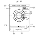
- FIG. 4 is an example of a display screen for displaying the hollow cone dark field of the transmission electron microscope 1. Various conditions can be changed by operating each configuration displayed on the display unit 15.
- the hollow cone dark field image of sample 10 is displayed in the image window 26 (displayed as "Image” in the figure).
- the hollow cone condition window 27 (displayed as “Hollow cone condition” in the figure) corresponds to the image window 26, and is composed of a display unit 27a and a condition setting unit 27b.
- a diffraction pattern acquired in advance, a diffraction pattern model of a material input in advance, or a diffraction pattern of a standard sample input in advance is displayed.
- Various conditions for acquiring a dark field image such as a ring scale display for each surface spacing, are displayed on the condition setting unit 27b, and each of these conditions can be operated.
- the image window 26 and the hollow cone condition window 27 are linked, and when the condition is changed in the condition setting unit 27b, the hollow cone dark field image also changes in the image window 26 in conjunction with the condition setting unit 27b.
- the hollow cone condition window 27 displays a diffraction pattern of the sample 10 (a pattern obtained by normal irradiation instead of hollow cone irradiation, or a pattern to be obtained).
- the diffraction region and the scattering region used for generating the hollow cone dark field image are displayed in a ring shape as the ring display 28.
- the region inside the ring display 28 is a region where the electron beam 25c is scheduled to pass through the objective movable diaphragm 18 when the hollow cone is irradiated. Therefore, the width of the ring display 28 (the difference between the outer diameter and the inner diameter of the ring display 28) corresponds to the diameter (diameter) of the objective movable diaphragm 18.
- the "width of the ring display 28" referred to here refers to the length of the portion of the reference numeral W shown in FIG.
- the diameter (radius) of the ring display 28 corresponds to the radius of the circle drawn by the electron beams 25b and 25c transmitted through the sample 10 by the hollow cone irradiation.
- the "diameter of the ring display 28" referred to here refers to the length of the portion of the reference numeral R shown in FIG. Ideally, the diameter R of the ring display 28 is the length from the optical axis to the midpoint (intermediate line) between the outer diameter and the inner diameter of the ring display 28.
- the condition setting unit 27b of the hollow cone condition window 27 has a scroll bar 30 for changing the diameter (radius) of the ring display 28, a cursor 30a for designating a value in the scroll bar 30, and a value specified by the cursor 30a.
- a neumeric box 31 for displaying the above and a button 32 for directly changing the value of the numeric box 31 are provided.
- the value specified here is the amount of current of the beam deflectors 22a and 22b, that is, the diameter of the ring display 28.
- the diameter of the ring display 28 in the hollow cone condition window 27 it is possible to specify which region of the electron beam (diffracted wave and / or scattered wave) is used to generate the hollow cone dark field image.
- the surface spacing corresponding to the average radius of the diffraction and scattering regions is displayed as the surface spacing display 29.
- the ring display 28, the surface spacing display 29, the position of the cursor 30a of the scroll bar 30, the numerical value of the numerical box 31, and the button 32 are linked, and the position of the cursor 30a of the scroll bar 30, the numerical value of the numerical box 31, or If any of the buttons 32 is changed, the others are also changed in conjunction with each other. Therefore, for example, the position of the cursor 30a of the scroll bar 30 can be automatically changed, and the hollow cone dark field image corresponding to the position of the cursor 30a can be observed and recorded as a moving image.
- the transmission electron microscope 1 in the first embodiment has a graphical user interface (GUI).
- GUI graphical user interface
- the graphical user interface includes an image window 26, a hollow cone condition window 27, a diffraction pattern, a ring display 28, a surface spacing display 29, a scroll bar 30, a cursor 30a, a numerical box 31 and a button 32 as described above.
- the contrast of the dark field image changes. For example, in the case of FIG. 4, when a diffraction spot or scattered electron beam is included inside the ring display 28, the corresponding region of the dark field image becomes bright, and the diffraction spot or scattering inside the ring display 28 becomes bright. When the electron beam is not included, the corresponding area of the dark field image becomes dark. What kind of dark-field image is obtained also depends on which diffraction spot or scattered electron beam is contained inside the ring display 28. Therefore, it is possible to record a desired hollow cone dark field image by stopping the cursor 30a when a desired contrast is obtained.
- the dark-field image is acquired while scanning (changing) the conditions for acquiring the dark-field image, and is most reflected in the signal strength of the dark-field image (in other words, of the image).
- the crystal lattice spacing range (which contributes most to the formation) may be determined.
- FIG. 6 shows a display screen corresponding to steps S1 to S5 shown in FIG.
- Step S1> the selected area diffraction pattern is captured in the hollow cone condition window 27. Diffraction spots having crystal lattice spacing used for the hollow cone dark field image are selected by the marker 33.
- the marker 33 has an arrow shape, but the shape of the marker 33 may be a circle having the diameter of the objective movable diaphragm 18 used for the hollow cone dark field image.
- the coordinates of the selected diffraction spot are transmitted to the image control unit 14 instructed by the microprocessor 24.
- the origin of the coordinate system is, for example, the coordinates of the optical axis (main spot).
- the image control unit 14 has a width corresponding to the diameter of the objective movable diaphragm 18 input in advance, and has a radius corresponding to the distance between the optical axis (main spot) and the diffraction spot.
- 28 is displayed on the diffraction pattern. In the display of the ring display 28, information may be transmitted to the image control unit 14. Along with the ring display 28, the position of the cursor 30a of the scroll bar 30, the numerical value of the numeric box 31, and the button 32 are also displayed in conjunction with each other.
- Each display such as the ring display 28 displayed on the hollow cone condition window 27 is displayed on the display unit 15.
- Step S3> The microprocessor 24 tilts the electron beam 25 by an angle ⁇ corresponding to the radius R of the ring display 28, and instructs the deflection coil control unit 23 to irradiate the sample 10 with a hollow cone. That is, the angle ⁇ of the precession motion of the electron beam 25 is determined by controlling the beam deflectors 22a and 22b based on the radius R of the ring display 28.
- each spot draws a circle with a designated radius R.
- Step S4> When the microprocessor 24 instructs the movable diaphragm control unit 20 to put the objective movable diaphragm 18 in the center of the optical axis, the movable diaphragm control unit 20 inserts the objective movable diaphragm 18 in the center of the optical axis.
- the images corresponding to steps S3 and S4 shown in FIG. 6 do not necessarily have to be displayed.
- Step S5> The electron beam 25 that has passed through the objective movable diaphragm 18 is imaged by the objective lens 4. After that, the electron beam 25 is magnified by the intermediate lenses 5a and 5b and the projection lenses 6a and 6b. Finally, the electron beam 25 is imaged by the camera 13.
- the signal (image) output by the camera 13 is displayed in the image window 26 as a dark field image by the image control unit 14 instructed by the microprocessor 24. Further, each condition when the dark field image and the dark field image are obtained is recorded in the image control unit 14 (image storage device 16).
- the diffraction spot group used for the hollow cone dark field image is selected by the marker 33, but the image window 26 is formed by changing the position of the cursor 30a of the scroll bar 30 or changing the numerical value of the numeric box 31. It is also possible to select the desired ring display 28 from the image displayed in.
- FIG. 7 is an example of the display screen in the first embodiment, and shows an example of the operation screen of the hollow cone dark field image of the transmission electron microscope 1.
- the example shown in FIG. 7 is suitable when a clear diffraction spot does not appear in the diffraction pattern and the diffraction pattern has a ring shape, for example, when observing a polycrystalline sample or an amorphous sample. However, even when a clear diffraction spot appears in the diffraction pattern, the application of the example of FIG. 7 is not hindered.
- the image control unit 14 is made to perform the following operations.
- the signal intensity line profile LI is a linear profile starting from the position of the main spot (position of the optical axis) of the diffraction pattern, and shows the distribution of the brightness of the diffraction pattern. That is, the signal intensity line profile LI is a curve in which a portion of the diffraction pattern in which the brightness is strong is provided as a peak (peak) of the convex waveform, and a plurality of convex waveforms are continuously connected. Further, the signal strength line profile LI may be displayed in the hollow cone condition window 27, may be displayed in another window, or may not be displayed.
- the position of the maximum peak of the signal intensity line profile LI is set as the center (optical axis) of the diameter of the ring display 28. Then, a plurality of ring displays 28 are set for each peak so that the distance R from the set optical axis to the position of each peak is the radius. The angle of the hollow cone irradiation is determined by the set ring display 28. The peak position may be selected by the user. On the other hand, when the image control unit 14 automatically determines the position of the peak, a plurality of annular displays 28 are automatically set for each peak, and the hollow cone dark field image is automatically and sequentially acquired.
- the image control unit 14 or the microprocessor 24 is made to automatically determine the peak position here, the user may determine the peak position by himself / herself.
- L ⁇ is a constant consisting of the product of the camera length L and the electron beam wavelength ⁇ , and is obtained by the setting conditions of the transmission electron microscope 1.
- the annular display 28 may be automatically set according to the calculated R, and the hollow cone dark field images may be acquired in order.
- FIGS. 8A, 8B, and 8C are examples of display screens according to the first embodiment, and show an example of an operation screen of a hollow cone dark field image of a transmission electron microscope 1.
- FIGS. 8A, 8B and 8C as in FIG. 7, a sample in which the diffraction spot does not clearly appear (a ring-shaped diffraction pattern appears) is used. However, it does not prevent the examples of FIGS. 8A, 8B and 8C from being applied to a sample in which the diffraction spot is clearly visible.
- the image control unit 14 is made to perform the following operations.
- the first annular display 28a used for the hollow cone dark field image is designated. It should be noted that this designation may be made by the user, or may be automatically made by the image control unit 14 by the method described with reference to FIG.
- the portion of the hollow cone dark field image to which the first annular display 28a contributes becomes bright. For example, the dark field DF1 indicated by shaded hatching becomes brighter.
- the portion of the hollow cone dark field image to which the second ring display 28b contributes is It gets brighter.
- the dark field DF2 indicated by a grid-like hatch that combines diagonal lines in two different directions becomes brighter.
- the example of FIG. 8 is useful for determining or estimating what diffracted wave is generated from which part of the sample. That is, the example of FIG. 8 is useful for determining or estimating which part of the sample is composed of what material and / or crystal structure.
- the display unit 15 can display a mapping image in which a plurality of dark field images are superimposed.
- the dark field DF1 and the dark field DF2 are shown by individual hatching.
- the dark field DF1 and the dark field DF2 may be displayed in different colors such as blue and yellow, respectively. If there is a point where the dark field DF1 and the dark field DF2 overlap, the point may be displayed by a neutral color in which blue and yellow are mixed.
- FIGS. 9A and 9B are examples of display screens in the first embodiment, and show an example of an operation screen of a hollow cone dark field image of a transmission electron microscope 1.
- the examples described in FIGS. 9A and 9B are suitable when the material of the sample to be inspected is known in advance, or when the material of the sample is almost estimated.
- the diffraction pattern model 35 of the specific material input in advance by the image control unit 14 is displayed. For example, by observing the amorphous sample 10 while heating it, it is possible to observe the process of crystallization from the amorphous sample.
- the diffraction pattern model of the sample 10 is displayed in advance, and a desired region is selected. Then, the intensity of the diffraction spot increases as the crystallization progresses, and although not shown here, in the image window 26, the signal intensity of the crystallized portion of the hollow cone dark-field image increases and the crystallized portion becomes brighter. , The crystallized part can be observed more clearly than the normal bright-field image.
- the ring scale 36 for each surface spacing according to the camera length setting and the surface showing the crystal plane spacing of the specific material are displayed in the hollow cone condition window 27.
- the interval display 29 may be displayed.
- the grid spacing d (reference numeral 37) corresponding to the ring display 28 is displayed.
- the ring scale 36 and the surface spacing display 29 are displayed according to the conditions of the material. I will do it. By doing so, when the material of the sample is as estimated, the characteristics of the sample can be quickly identified, so that the inspection time can be significantly shortened. Further, even if the material of the sample is not as estimated, at least the estimated material can be excluded from the inspection target. Further, by displaying the ring scale 36 and the surface spacing display 29, the user can know the guideline of the condition at a glance, so that the burden on the user can be reduced.
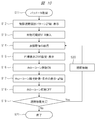
- Step S11> the microprocessor 24 sets the accelerating voltage, the camera length, the size of the limited visual field movable diaphragm 19, the size of the objective movable diaphragm 18, and the position of the sample 10 which are parameters necessary for acquiring the hollow cone dark field image. Obtained from the control unit.
- Step S12> Each lens system is switched so that the mode for observing the selected area diffraction pattern is set, and the selected area diffraction pattern is displayed in the image window 26.
- This selected area diffraction pattern is acquired and recorded on the display unit 15 and displayed on the hollow cone condition window 27.
- the limited visual field working diaphragm 19 is inserted in the desired region, but the objective movable diaphragm 18 is not inserted.
- the optical axis (main spot) of the selected area diffraction pattern is adjusted to be displayed in the center of the image window 26.
- the movable diaphragm control unit 20 inserts the objective movable diaphragm 18 into the position of the optical axis, that is, in the center of the image window 26.
- the limited visual field movable diaphragm 19 is controlled so as to be out of the visual field.
- Step S14> The lens power control unit 8 switches from the mode of observing the selected area diffraction pattern to the image observation mode, and the bright field image is displayed in the image window 26. This bright field image is recorded in the image control unit 14 (image storage device 16).
- Step S15 When the diffraction spot to be used for the hollow cone dark field image is selected from the diffraction patterns displayed in the hollow cone condition window 27, the image control unit 14 sets the ring display 28, and the hollow cone condition window 27 displays the ring. 28 is displayed.
- Step S17> The hollow cone dark field image is displayed in the image window 26, and the hollow cone dark field image and the imaging conditions (acceleration voltage, magnification, etc.) of the hollow cone condition window 27 are recorded in the image control unit 14 (image storage device 16).
- Step S19 to S21> It is determined whether the work is completed or whether it is necessary to acquire another visual field. If it is not necessary to acquire another visual field, the process proceeds to step S21 (No), and the inspection is completed. For example, in the case of recording only one field of view, or when the last recording of the recordings in a plurality of fields of view is completed, the process proceeds to step S21 (No). When it is necessary to acquire another visual field, the process proceeds to step S22 (Yes), and steps S14 to S19 are performed again.
- step S19 may be made by the user at the end of step S18, or may be set in advance so as to automatically record only one visual field or a plurality of visual fields.
- the beam deflectors 21a and 21b or the beam deflectors 22a and 22b are used to prevent the electron beam 25 from irradiating the sample 10 (blanking). This makes it possible to prevent the sample 10 from being damaged by the irradiation of the electron beam 25.
- the operation settings of the beam deflectors 21a and 21b or the beam deflectors 22a and 22b may be set when the field of view is switched so that the blanking is automatically performed.
- FIG. 11 shows an inspection method in the case of acquiring and recording a hollow cone dark field using a plurality of ring displays 28.
- the explanations of the parts that overlap with the explanations in FIG. 10 are omitted.
- Step S22> For example, when a plurality of ring displays 28 are used, it is determined whether or not to change the ring display 28 after performing steps S11 to S18 shown in FIG. For example, if the next ring display 28 having a different radius is planned to be used, the process proceeds to step S15 (Yes), the next ring display 28 is reset, and the reset ring display 28 is displayed. Using, steps S15 to S22 are performed again. When all the ring displays 28 are used, the process proceeds to step S23 (No).
- step S15 the next ring display 28 is reset, and steps S15 to S22 are performed again using the reset ring display 28.
- step S20 of FIG. 28 when resetting the ring display 28, it is preferable to perform blanking in the same manner as in step S20 of FIG. That is, since the angle of the precession movement of the electron beam 25 is changed by resetting the ring display 28, it is preferable that the electron beam 25 does not irradiate the sample 10 within this change period. This can prevent the sample 10 from being damaged.
- step S23 As in step S19 in FIG. 10, it is determined whether or not it is necessary to acquire another visual field. If it is not necessary to acquire another visual field, the process proceeds to step S25 (No), and the work is completed. When it is necessary to acquire another field of view, the process proceeds to step S24 (Yes), and steps S14 to S23 are performed again.
- step S23 may be made by the user at the end of step S22, or may be set in advance so as to automatically record only one visual field or a plurality of visual fields.
- the present invention has been specifically described above based on the embodiment for carrying out the present invention, but the present invention is not limited to the above-described embodiment and can be variously modified without departing from the gist thereof.
- the terms "diameter” and “radius” appear in the present application, the diameter has a value twice the radius. Therefore, “specifying a diameter” is equivalent or equal to “specifying a radius” and vice versa.
Landscapes
- Chemical & Material Sciences (AREA)
- Analytical Chemistry (AREA)
- Physics & Mathematics (AREA)
- Health & Medical Sciences (AREA)
- Life Sciences & Earth Sciences (AREA)
- Biochemistry (AREA)
- General Health & Medical Sciences (AREA)
- General Physics & Mathematics (AREA)
- Immunology (AREA)
- Pathology (AREA)
- Crystallography & Structural Chemistry (AREA)
- Analysing Materials By The Use Of Radiation (AREA)
Priority Applications (3)
| Application Number | Priority Date | Filing Date | Title |
|---|---|---|---|
| PCT/JP2019/017938 WO2020217456A1 (ja) | 2019-04-26 | 2019-04-26 | 透過電子顕微鏡および透過電子顕微鏡を用いた検査方法 |
| US17/594,658 US12170184B2 (en) | 2019-04-26 | 2019-04-26 | Transmission electron microscope and inspection method using transmission electron microscope |
| JP2021515690A JP7182700B2 (ja) | 2019-04-26 | 2019-04-26 | 透過電子顕微鏡および透過電子顕微鏡を用いた検査方法 |
Applications Claiming Priority (1)
| Application Number | Priority Date | Filing Date | Title |
|---|---|---|---|
| PCT/JP2019/017938 WO2020217456A1 (ja) | 2019-04-26 | 2019-04-26 | 透過電子顕微鏡および透過電子顕微鏡を用いた検査方法 |
Publications (1)
| Publication Number | Publication Date |
|---|---|
| WO2020217456A1 true WO2020217456A1 (ja) | 2020-10-29 |
Family
ID=72940918
Family Applications (1)
| Application Number | Title | Priority Date | Filing Date |
|---|---|---|---|
| PCT/JP2019/017938 Ceased WO2020217456A1 (ja) | 2019-04-26 | 2019-04-26 | 透過電子顕微鏡および透過電子顕微鏡を用いた検査方法 |
Country Status (3)
| Country | Link |
|---|---|
| US (1) | US12170184B2 (https=) |
| JP (1) | JP7182700B2 (https=) |
| WO (1) | WO2020217456A1 (https=) |
Cited By (1)
| Publication number | Priority date | Publication date | Assignee | Title |
|---|---|---|---|---|
| WO2025248762A1 (ja) * | 2024-05-31 | 2025-12-04 | 株式会社日立ハイテク | 透過電子顕微鏡システム |
Families Citing this family (1)
| Publication number | Priority date | Publication date | Assignee | Title |
|---|---|---|---|---|
| WO2022219699A1 (ja) * | 2021-04-13 | 2022-10-20 | 株式会社日立ハイテク | 透過型電子顕微鏡 |
Citations (2)
| Publication number | Priority date | Publication date | Assignee | Title |
|---|---|---|---|---|
| JPS60105150A (ja) * | 1983-11-11 | 1985-06-10 | Jeol Ltd | 電子顕微鏡 |
| JPS60150548A (ja) * | 1984-01-17 | 1985-08-08 | Jeol Ltd | 電子線回折方法 |
Family Cites Families (2)
| Publication number | Priority date | Publication date | Assignee | Title |
|---|---|---|---|---|
| US7608238B2 (en) * | 2006-02-17 | 2009-10-27 | International University Bremen Gmbh | Nanosheets of MgO processing the 111 plane |
| JP7193694B2 (ja) * | 2018-07-26 | 2022-12-21 | 国立研究開発法人理化学研究所 | 電子顕微鏡およびそれを用いた試料観察方法 |
-
2019
- 2019-04-26 US US17/594,658 patent/US12170184B2/en active Active
- 2019-04-26 WO PCT/JP2019/017938 patent/WO2020217456A1/ja not_active Ceased
- 2019-04-26 JP JP2021515690A patent/JP7182700B2/ja active Active
Patent Citations (2)
| Publication number | Priority date | Publication date | Assignee | Title |
|---|---|---|---|---|
| JPS60105150A (ja) * | 1983-11-11 | 1985-06-10 | Jeol Ltd | 電子顕微鏡 |
| JPS60150548A (ja) * | 1984-01-17 | 1985-08-08 | Jeol Ltd | 電子線回折方法 |
Cited By (1)
| Publication number | Priority date | Publication date | Assignee | Title |
|---|---|---|---|---|
| WO2025248762A1 (ja) * | 2024-05-31 | 2025-12-04 | 株式会社日立ハイテク | 透過電子顕微鏡システム |
Also Published As
| Publication number | Publication date |
|---|---|
| US12170184B2 (en) | 2024-12-17 |
| JP7182700B2 (ja) | 2022-12-02 |
| JPWO2020217456A1 (https=) | 2020-10-29 |
| US20220244201A1 (en) | 2022-08-04 |
Similar Documents
| Publication | Publication Date | Title |
|---|---|---|
| JP3888980B2 (ja) | 物質同定システム | |
| CN106482634B (zh) | 使用机器视觉检验系统中的可调谐透镜的多等级图像聚焦 | |
| JP6255494B2 (ja) | 電子顕微鏡、及び、試料の観察方法 | |
| JP5743950B2 (ja) | 走査電子顕微鏡 | |
| TWI592976B (zh) | Charged particle beam device and inspection method using the device | |
| US5298747A (en) | Scanning interference electron microscopy | |
| JP3980856B2 (ja) | 電子顕微鏡における分析方法 | |
| JP2007207688A (ja) | ミラー電子顕微鏡およびミラー電子顕微鏡を用いた検査装置 | |
| JP7182700B2 (ja) | 透過電子顕微鏡および透過電子顕微鏡を用いた検査方法 | |
| JP2006173027A (ja) | 走査透過電子顕微鏡、及び収差測定方法、ならびに収差補正方法 | |
| US6677585B2 (en) | Scanning charged particle microscope, and focal distance adjusting method and astigmatism correction method thereof | |
| JPH10172490A (ja) | 走査電子顕微鏡 | |
| JP2005235665A (ja) | 暗視野走査透過電子顕微鏡および観察方法 | |
| JP6716026B2 (ja) | 荷電粒子線装置および荷電粒子線装置における条件設定方法 | |
| WO2020115876A1 (ja) | 荷電粒子線装置 | |
| JP4413887B2 (ja) | 物質同定システム | |
| EP3591686B1 (en) | Electron microscope | |
| JP2023007094A (ja) | 走査電子顕微鏡 | |
| KR101167565B1 (ko) | Tem의 3차원 회절패턴분석을 위한 정밀 제어용 전자빔의 회전각도 및 회전속도 제어-표시 시스템 | |
| JP2011076813A (ja) | 走査透過電子顕微鏡および走査透過像観察方法 | |
| JP2006156134A (ja) | 反射結像型電子顕微鏡 | |
| JP2004095192A (ja) | 電子顕微鏡 | |
| JP5174483B2 (ja) | 荷電粒子ビーム装置、及び試料の表面の帯電状態を知る方法 | |
| JP4275786B2 (ja) | 電子顕微鏡 | |
| WO2021044544A1 (ja) | 試料画像表示システムおよび荷電粒子線装置 |
Legal Events
| Date | Code | Title | Description |
|---|---|---|---|
| 121 | Ep: the epo has been informed by wipo that ep was designated in this application |
Ref document number: 19925703 Country of ref document: EP Kind code of ref document: A1 |
|
| ENP | Entry into the national phase |
Ref document number: 2021515690 Country of ref document: JP Kind code of ref document: A |
|
| NENP | Non-entry into the national phase |
Ref country code: DE |
|
| 122 | Ep: pct application non-entry in european phase |
Ref document number: 19925703 Country of ref document: EP Kind code of ref document: A1 |