WO2020208871A1 - 光モジュール - Google Patents
光モジュール Download PDFInfo
- Publication number
- WO2020208871A1 WO2020208871A1 PCT/JP2019/049891 JP2019049891W WO2020208871A1 WO 2020208871 A1 WO2020208871 A1 WO 2020208871A1 JP 2019049891 W JP2019049891 W JP 2019049891W WO 2020208871 A1 WO2020208871 A1 WO 2020208871A1
- Authority
- WO
- WIPO (PCT)
- Prior art keywords
- light
- mirror
- laser diode
- mems
- optical module
- Prior art date
- Legal status (The legal status is an assumption and is not a legal conclusion. Google has not performed a legal analysis and makes no representation as to the accuracy of the status listed.)
- Ceased
Links
Images




Classifications
-
- G—PHYSICS
- G02—OPTICS
- G02B—OPTICAL ELEMENTS, SYSTEMS OR APPARATUS
- G02B26/00—Optical devices or arrangements for the control of light using movable or deformable optical elements
- G02B26/08—Optical devices or arrangements for the control of light using movable or deformable optical elements for controlling the direction of light
- G02B26/10—Scanning systems
- G02B26/105—Scanning systems with one or more pivoting mirrors or galvano-mirrors
-
- G—PHYSICS
- G02—OPTICS
- G02B—OPTICAL ELEMENTS, SYSTEMS OR APPARATUS
- G02B26/00—Optical devices or arrangements for the control of light using movable or deformable optical elements
- G02B26/08—Optical devices or arrangements for the control of light using movable or deformable optical elements for controlling the direction of light
- G02B26/10—Scanning systems
- G02B26/101—Scanning systems with both horizontal and vertical deflecting means, e.g. raster or XY scanners
-
- G—PHYSICS
- G02—OPTICS
- G02B—OPTICAL ELEMENTS, SYSTEMS OR APPARATUS
- G02B26/00—Optical devices or arrangements for the control of light using movable or deformable optical elements
- G02B26/08—Optical devices or arrangements for the control of light using movable or deformable optical elements for controlling the direction of light
- G02B26/0816—Optical devices or arrangements for the control of light using movable or deformable optical elements for controlling the direction of light by means of one or more reflecting elements
- G02B26/0833—Optical devices or arrangements for the control of light using movable or deformable optical elements for controlling the direction of light by means of one or more reflecting elements the reflecting element being a micromechanical device, e.g. a MEMS mirror, DMD
-
- G—PHYSICS
- G02—OPTICS
- G02B—OPTICAL ELEMENTS, SYSTEMS OR APPARATUS
- G02B7/00—Mountings, adjusting means, or light-tight connections, for optical elements
- G02B7/18—Mountings, adjusting means, or light-tight connections, for optical elements for prisms; for mirrors
- G02B7/181—Mountings, adjusting means, or light-tight connections, for optical elements for prisms; for mirrors with means for compensating for changes in temperature or for controlling the temperature; thermal stabilisation
-
- H—ELECTRICITY
- H01—ELECTRIC ELEMENTS
- H01S—DEVICES USING THE PROCESS OF LIGHT AMPLIFICATION BY STIMULATED EMISSION OF RADIATION [LASER] TO AMPLIFY OR GENERATE LIGHT; DEVICES USING STIMULATED EMISSION OF ELECTROMAGNETIC RADIATION IN WAVE RANGES OTHER THAN OPTICAL
- H01S5/00—Semiconductor lasers
- H01S5/02—Structural details or components not essential to laser action
- H01S5/022—Mountings; Housings
-
- H—ELECTRICITY
- H01—ELECTRIC ELEMENTS
- H01S—DEVICES USING THE PROCESS OF LIGHT AMPLIFICATION BY STIMULATED EMISSION OF RADIATION [LASER] TO AMPLIFY OR GENERATE LIGHT; DEVICES USING STIMULATED EMISSION OF ELECTROMAGNETIC RADIATION IN WAVE RANGES OTHER THAN OPTICAL
- H01S5/00—Semiconductor lasers
- H01S5/02—Structural details or components not essential to laser action
- H01S5/022—Mountings; Housings
- H01S5/023—Mount members, e.g. sub-mount members
- H01S5/02315—Support members, e.g. bases or carriers
-
- H—ELECTRICITY
- H04—ELECTRIC COMMUNICATION TECHNIQUE
- H04N—PICTORIAL COMMUNICATION, e.g. TELEVISION
- H04N5/00—Details of television systems
- H04N5/74—Projection arrangements for image reproduction, e.g. using eidophor
-
- H—ELECTRICITY
- H01—ELECTRIC ELEMENTS
- H01S—DEVICES USING THE PROCESS OF LIGHT AMPLIFICATION BY STIMULATED EMISSION OF RADIATION [LASER] TO AMPLIFY OR GENERATE LIGHT; DEVICES USING STIMULATED EMISSION OF ELECTROMAGNETIC RADIATION IN WAVE RANGES OTHER THAN OPTICAL
- H01S5/00—Semiconductor lasers
- H01S5/005—Optical components external to the laser cavity, specially adapted therefor, e.g. for homogenisation or merging of the beams or for manipulating laser pulses, e.g. pulse shaping
- H01S5/0071—Optical components external to the laser cavity, specially adapted therefor, e.g. for homogenisation or merging of the beams or for manipulating laser pulses, e.g. pulse shaping for beam steering, e.g. using a mirror outside the cavity to change the beam direction
-
- H—ELECTRICITY
- H01—ELECTRIC ELEMENTS
- H01S—DEVICES USING THE PROCESS OF LIGHT AMPLIFICATION BY STIMULATED EMISSION OF RADIATION [LASER] TO AMPLIFY OR GENERATE LIGHT; DEVICES USING STIMULATED EMISSION OF ELECTROMAGNETIC RADIATION IN WAVE RANGES OTHER THAN OPTICAL
- H01S5/00—Semiconductor lasers
- H01S5/02—Structural details or components not essential to laser action
- H01S5/022—Mountings; Housings
- H01S5/02208—Mountings; Housings characterised by the shape of the housings
- H01S5/02212—Can-type, e.g. TO-CAN housings with emission along or parallel to symmetry axis
-
- H—ELECTRICITY
- H01—ELECTRIC ELEMENTS
- H01S—DEVICES USING THE PROCESS OF LIGHT AMPLIFICATION BY STIMULATED EMISSION OF RADIATION [LASER] TO AMPLIFY OR GENERATE LIGHT; DEVICES USING STIMULATED EMISSION OF ELECTROMAGNETIC RADIATION IN WAVE RANGES OTHER THAN OPTICAL
- H01S5/00—Semiconductor lasers
- H01S5/02—Structural details or components not essential to laser action
- H01S5/022—Mountings; Housings
- H01S5/0225—Out-coupling of light
- H01S5/02255—Out-coupling of light using beam deflecting elements
-
- H—ELECTRICITY
- H01—ELECTRIC ELEMENTS
- H01S—DEVICES USING THE PROCESS OF LIGHT AMPLIFICATION BY STIMULATED EMISSION OF RADIATION [LASER] TO AMPLIFY OR GENERATE LIGHT; DEVICES USING STIMULATED EMISSION OF ELECTROMAGNETIC RADIATION IN WAVE RANGES OTHER THAN OPTICAL
- H01S5/00—Semiconductor lasers
- H01S5/40—Arrangement of two or more semiconductor lasers, not provided for in groups H01S5/02 - H01S5/30
- H01S5/4025—Array arrangements, e.g. constituted by discrete laser diodes or laser bar
- H01S5/4087—Array arrangements, e.g. constituted by discrete laser diodes or laser bar emitting more than one wavelength
- H01S5/4093—Red, green and blue [RGB] generated directly by laser action or by a combination of laser action with nonlinear frequency conversion
Definitions
- This disclosure relates to an optical module.
- An optical module including a light emitting unit that emits light from a semiconductor light emitting element and a scanning unit that scans light from the light emitting unit is known (see, for example, Patent Documents 1 to 3).
- Such an optical module can draw an image such as a character or a figure by two-dimensionally scanning the light from the light emitting unit along a desired path.
- An optical module includes a light forming portion configured to form light, and a protective member that surrounds the light forming portion and seals the light forming portion.
- the light forming unit includes a laser diode and a first mirror having a first reflecting surface that reflects light from the laser diode so as to scan the light, and is a normal of the first normal that is a normal at the center point of the first reflecting surface.
- a first MEMS Micro Electrical Mechanical Systems
- the first mirror swings so as to form a first plane according to a trajectory
- a second mirror having a second reflecting surface that reflects light from the first mirror so as to scan it. It includes a second MEMS in which the second mirror swings so as to form a second plane orthogonal to the first plane by the locus of the second normal, which is the normal at the center point of the second reflecting surface.
- FIG. 1 is a schematic perspective view showing the structure of the optical module according to the first embodiment.
- FIG. 2 is a schematic perspective view showing the structure of the optical module of the first embodiment with the cap removed.
- FIG. 3 is a schematic perspective view showing the structure of the optical module of the first embodiment with the cap removed.
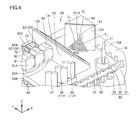
- FIG. 4 is a diagram showing a first plane formed by the first mirror.
- FIG. 5 is a diagram showing a second plane formed by the second mirror.
- FIG. 6 is a schematic view showing the structure of the optical module according to the first embodiment.
- FIG. 7 is a schematic view showing the structure of the optical module according to the first embodiment.
- FIG. 8 is a schematic perspective view showing the structure of the optical module according to the second embodiment.
- FIG. 1 is a schematic perspective view showing the structure of the optical module according to the first embodiment.
- FIG. 2 is a schematic perspective view showing the structure of the optical module of the first embodiment with the cap removed.
- FIG. 3 is a schematic perspective view showing the structure of the optical
- FIG. 9 is a schematic perspective view showing the structure of the optical module of the second embodiment with the cap removed.
- FIG. 10 is a schematic perspective view showing the structure of the optical module of the second embodiment with the cap removed.
- FIG. 11 is a diagram showing a first plane formed by the first mirror.
- FIG. 12 is a diagram showing a second plane formed by the second mirror.
- FIG. 13 is a schematic view showing the structure of the optical module according to the second embodiment.
- FIG. 14 is a schematic view showing the structure of the optical module according to the second embodiment.
- the optical module is required to be miniaturized.
- the scanning unit includes a mirror that scans the light from the light emitting unit by swinging.
- the fluctuation may propagate in the vertical direction due to the influence of the fluctuation in the horizontal direction, for example. In such a case, it becomes difficult to control the mirror, and it becomes difficult to draw an image properly.
- one of the purposes is to provide an optical module that can easily control the mirror and can draw two-dimensionally while achieving miniaturization.
- the optical module of the present disclosure includes a light forming portion configured to form light, and a protective member that surrounds the light forming portion and seals the light forming portion.
- the light forming unit includes a laser diode and a first mirror having a first reflecting surface that reflects light from the laser diode so as to scan the light, and is a normal of the first normal that is a normal at the center point of the first reflecting surface.
- the second reflecting surface includes a first MEMS in which the first mirror swings so as to form a first plane according to a locus, and a second mirror having a second reflecting surface that reflects light from the first mirror so as to scan. Includes a second MEMS in which the second mirror swings to form a second plane orthogonal to the first plane by the locus of the second normal, which is the normal at the center point of.
- the laser diode, the first MEMS and the second MEMS are sealed by a protective member. Therefore, the size can be reduced as compared with the optical module in which the laser diode, the first MEMS and the second MEMS, each of which is sealed in the package, are combined.
- the optical module of the present disclosure includes a first MEMS including a first mirror and a second MEMS including a second mirror. The first mirror swings so as to form a first plane according to the locus of the first normal. The second mirror swings so as to form a second plane orthogonal to the first plane by the locus of the second normal. Therefore, the light can be scanned two-dimensionally by the first mirror and the second mirror.
- the optical module of the present disclosure it is possible to easily control the mirror and perform two-dimensional drawing while achieving miniaturization.
- the center points of the first reflecting surface and the second reflecting surface are perpendicular to the plane including the outer edges of the first reflecting surface and the second reflecting surface with respect to the first reflecting surface and the second reflecting surface.
- the optical forming unit may further include a base member including an electronic temperature adjusting module.
- the first MEMS and the second MEMS may be arranged on the base member.
- the deflection angle of the first mirror and the second mirror may fluctuate depending on the temperature.
- the temperature of the first MEMS and the second MEMS can be adjusted to an appropriate range by the electronic temperature adjusting module included in the base member. Therefore, the stability of the operation of the first MEMS and the second MEMS with respect to the temperature change can be improved.
- the optical forming unit may further include a plurality of laser diodes and a filter that combines the light emitted from the plurality of laser diodes.
- the light forming unit may further include a plurality of filters that combine the light emitted from the plurality of laser diodes.
- the plurality of laser diodes may include a first laser diode that emits a first light, a second laser diode that emits a second light, and a third laser diode that emits a third light.
- the plurality of filters are combined by the first member and the first member that combine the first light emitted from the first laser diode and the second light emitted from the second laser diode.
- a second member that combines the first light and the second light with the third light emitted from the third laser diode may be included.
- the first laser diode may be a red laser diode that emits red light.
- the second laser diode may be a green laser diode that emits green light.
- the third laser diode may be a blue laser diode that emits blue light. With such a configuration, light of a desired color can be formed.
- FIG. 1 is a schematic perspective view showing the structure of the optical module according to the first embodiment.
- FIG. 2 is a perspective view corresponding to a state in which the cap of FIG. 1 is removed.
- FIG. 3 is a perspective view taken from a viewpoint different from that of FIG. 2, corresponding to the state in which the cap of FIG. 1 is removed.
- FIG. 6 is a schematic view of the cap 40 in a cross section and other parts in a plan view in an XY plane.
- FIG. 7 is a schematic view of the cap 40 and the glass plate 42 in a cross section and other parts in a plan view in an XX plane.
- the optical module 1 in the present embodiment includes a light forming portion 20 that forms light and a protective member 2 that surrounds the light forming portion 20 and seals the light forming portion 20.
- the protective member 2 includes a base portion 10 as a base body and a cap 40 which is a lid portion welded to the base portion 10. That is, the light forming portion 20 is hermetically sealed by the protective member 2.
- the base 10 has a flat plate shape.
- the light forming portion 20 is arranged on one main surface 10A of the base portion 10.
- the cap 40 is arranged in contact with one main surface 10A of the base 10 so as to cover the light forming portion 20.
- a plurality of lead pins 51 are installed on the base 10 so as to penetrate from the other main surface 10B side of the base 10 to the one main surface 10A side and project to both sides of the one main surface 10A side and the other main surface 10B side.
- the space surrounded by the base 10 and the cap 40 is filled with a gas having reduced (removed) moisture such as dry air.
- the cap 40 is formed with a window portion 40A so as to penetrate the cap 40 in a region of the base portion 10 facing the main surface 10A.
- the glass plate 42 is arranged so as to close the window portion 40A.
- the glass plate 42 has a flat plate shape.
- the protective member 2 is an airtight member that keeps the inside airtight.
- the window portion 40A in the region of the base portion 10 of the cap 40 facing the main surface 10A in this way, the stress applied to the glass plate 42 when the cap 40 is welded to the base portion 10 can be reduced. .. Therefore, the inside of the protective member 2 can be kept in a good airtight state.
- the light forming unit 20 includes a base member 4, laser diodes 81, 82, 83, filters 97, 98, 99, MEMS 120, 130, and a third mirror 21. Including.
- the base member 4 includes an electronic temperature control module 30, a base plate 60, a MEMS base 64, 65, and a pedestal 66.
- the electronic temperature control module 30 includes a heat absorbing plate 31 and a heat radiating plate 33 having a flat plate shape, and a semiconductor column 32 arranged side by side between the heat absorbing plate 31 and the heat radiating plate 33 with an electrode interposed therebetween.
- the heat absorbing plate 31 and the heat radiating plate 33 are made of, for example, alumina.
- the electronic temperature adjustment module 30 is arranged on one main surface 10A of the base 10 so that the heat radiating plate 33 comes into contact with one main surface 10A of the base 10.
- the base plate 60, the MEMS bases 64 and 65, and the pedestal 66 are arranged on the heat absorbing plate 31 so as to come into contact with the heat absorbing plate 31.
- the base plate 60 has a plate-like shape.
- the base plate 60 has one main surface 60A having a rectangular shape when viewed in a plane.
- One main surface 60A of the base plate 60 includes a lens mounting area 61, a chip mounting area 62, and a filter mounting area 63.
- the chip mounting area 62 includes a first area 62A, a second area 62B, and a third area 62C.
- the first region 62A, the second region 62B, and the third region 62C are formed along one side of the main surface 60A.
- the first region 62A, the second region 62B, and the third region 62C are formed at intervals in the X-axis direction.
- the lens mounting area 61 is adjacent to the chip mounting area 62 and is arranged along the chip mounting area 62.
- the filter mounting area 63 is arranged along the other side in a region including the other side facing the one side of one main surface 60A.
- the chip mounting area 62, the lens mounting area 61, and the filter mounting area 63 are parallel to each other.
- the thickness of the base plate 60 in the first region 62A, the second region 62B, and the third region 62C of the chip mounting region 62 is larger than that in the lens mounting region 61 and the filter mounting region 63.
- the thickness of the base plate 60 in the lens mounting area 61 and the thickness of the base plate 60 in the filter mounting area 63 are equal.
- the lens mounting area 61 and the filter mounting area 63 are included in the same plane.
- the heights of the first region 62A, the second region 62B, and the third region 62C (the height based on the lens mounting region 61, that is, the lens mounting region 61) as compared with the lens mounting region 61 and the filter mounting region 63.
- the height in the direction perpendicular to is higher.
- a first submount 71, a second submount 72, and a third submount 73 are formed in a flat plate shape, respectively, on one of the main surfaces 60A. They are arranged side by side along the sides.
- the second submount 72 is arranged so as to be sandwiched between the first submount 71 and the third submount 73.
- a chip-shaped red laser diode 81 as the first laser diode 101 is arranged on the first submount 71.
- the chip shape means a state in which the package is not sealed.
- a chip-shaped green laser diode 82 as the second laser diode 102 is arranged on the second submount 72.
- a chip-shaped blue laser diode 83 as the third laser diode 103 is arranged on the third submount 73.
- Height of the optical axis of the red laser diode 81, the green laser diode 82, and the blue laser diode 83 (distance between the reference plane and the optical axis when the lens mounting area 61 of one main surface 60A is used as the reference plane; Z-axis direction The distance from the reference plane in the above) is adjusted and matched by the first submount 71, the second submount 72, and the third submount 73.
- the first lens 91, the second lens 92, and the third lens 93 are arranged on the lens mounting area 61.
- the first lens 91, the second lens 92, and the third lens 93 have lens portions 91A, 92A, and 93A whose surfaces are lens surfaces, respectively.
- the lens portions 91A, 92A, 93A and the regions other than the lens portions 91A, 92A, 93A are integrally molded.
- the central axes of the lens portions 91A, 92A, 93A of the first lens 91, the second lens 92, and the third lens 93 that is, the optical axes of the lens portions 91A, 92A, 93A are the red laser diode 81, the green laser diode 82, and the green laser diode 82, respectively. It coincides with the optical axis of the blue laser diode 83.
- the first lens 91, the second lens 92, and the third lens 93 convert the spot size of the light emitted from the red laser diode 81, the green laser diode 82, and the blue laser diode 83, respectively (the beam shape on a certain projection surface). Shape it into the desired shape).
- the light emitted from the red laser diode 81, the green laser diode 82, and the blue laser diode 83 is converted into collimated light by the first lens 91, the second lens 92, and the third lens 93.
- the first filter 97, the second filter 98 as the first member 111, and the third filter 99 as the second member 112 are arranged on the filter mounting area 63.
- the first filter 97 is arranged on a straight line connecting the red laser diode 81 and the first lens 91.
- the second filter 98 is arranged on a straight line connecting the green laser diode 82 and the second lens 92.
- the third filter 99 is arranged on a straight line connecting the blue laser diode 83 and the third lens 93.
- the first filter 97, the second filter 98, and the third filter 99 each have a flat plate shape having parallel main surfaces.
- the first filter 97, the second filter 98 and the third filter 99 are, for example, wavelength selective filters.
- the first filter 97, the second filter 98 and the third filter 99 are, for example, a dielectric multilayer filter.
- the first filter 97 reflects red light.
- the second filter 98 transmits red light and reflects green light.
- the third filter 99 transmits red light and green light and reflects blue light.
- the first filter 97, the second filter 98, and the third filter 99 selectively transmit and reflect light having a specific wavelength.
- the first filter 97, the second filter 98, and the third filter 99 combine the light emitted from the red laser diode 81, the green laser diode 82, and the blue laser diode 83.
- the red laser diode 81, the lens portion 91A of the first lens 91, and the first filter 97 are aligned in a straight line along the light emission direction of the red laser diode 81 (aligned in the Y-axis direction). ) Have been placed.
- the green laser diode 82, the lens portion 92A of the second lens 92, and the second filter 98 are arranged side by side (aligned in the Y-axis direction) on a straight line along the light emission direction of the green laser diode 82.
- the blue laser diode 83, the lens portion 93A of the third lens 93, and the third filter 99 are arranged side by side (aligned in the Y-axis direction) on a straight line along the light emission direction of the blue laser diode 83.
- the emission direction of the red laser diode 81, the emission direction of the green laser diode 82, and the emission direction of the blue laser diode 83 are parallel to each other.
- the main surfaces of the first filter 97, the second filter 98, and the third filter 99 are inclined by 45 ° with respect to the emission direction (Y-axis direction) of the red laser diode 81, the green laser diode 82, and the blue laser diode 83, respectively. There is.
- the pedestal 66 has a columnar shape.
- the pedestal 66 is arranged on the heat absorbing plate 31.
- the pedestal 66 and the base plate 60 are arranged at intervals in the X-axis direction.
- a third mirror 21 is arranged on the pedestal 66.
- the third mirror 21 has a third reflecting surface 21A that reflects the light combined by the filters 97, 98, 99.
- the third mirror 21 and the filters 97, 98, 99 are arranged side by side along the X-axis direction.
- the third mirror 21 is arranged so that the third reflecting surface 21A is located in a region corresponding to the optical path of the light waved by the filters 97, 98, 99.
- the first MEMS base 64 and the second MEMS base 65 have a triangular prism (rectangular prism) shape.
- the first MEMS base 64 is arranged on the heat absorbing plate 31 so as to come into contact with the heat absorbing plate 31 on one bottom surface of the triangular prism.
- the second MEMS base 65 is arranged on the heat absorbing plate 31 so as to come into contact with the heat absorbing plate 31 on one side surface of the triangular prism.
- the first MEMS base 64 and the pedestal 66 are arranged at intervals in the Y-axis direction.
- the second MEMS base 65 is arranged between the base plate 60 and the first MEMS base 64 in the X-axis direction.
- a first MEMS 120 including a first mirror 121 is arranged on one side surface of the first MEMS base 64.
- the first MEMS 120 is a piezoelectric MEMS. By doing so, the runout angle of the first mirror 121 can be increased.
- the first mirror 121 has a disk-like shape.
- the first MEMS 120 is arranged so that the first mirror 121 is located in a region corresponding to the optical path of the light reflected by the third reflecting surface 21A of the third mirror 21.
- the first mirror 121 has a first reflecting surface 121A that reflects the light reflected by the third reflecting surface 21A.
- the first mirror 121 is swung so as to form a first planar U 1 by a first locus of normal T 1 is normal at the center point G 1 of the first reflecting surface 121A.
- the center point of the first reflecting surface 121A is when the swing axis 122 of the first mirror 121 is projected onto the first reflecting surface 121A in a direction perpendicular to the plane including the outer edge of the first reflecting surface 121A.
- the first mirror 121 swings due to resonance.
- the resonance frequency of the first mirror 121 is, for example, 20 kHz or more.
- the light reflected by the third reflecting surface 21A can be scanned by the first MEMS 120 including the first mirror 121.
- the resonance frequency of the first mirror 121 may be set to 30 kHz or more. In this way, the resonance frequency can be increased by using the first MEMS 120 that swings in one direction.
- a second MEMS 130 including a second mirror 131 is arranged on the other side surface of the second MEMS base 65.
- the second mirror 131 has a flat plate shape.
- the second mirror 131 has a rectangular shape when viewed in a plane in a direction perpendicular to the other side surface of the second MEMS base 65.
- the second MEMS 130 is arranged so that the second mirror 131 is located in the region corresponding to the optical path of the light scanned by the first mirror 121.
- the second MEMS 130 is a piezoelectric MEMS. By doing so, the runout angle of the second mirror 131 can be increased.
- the second mirror 131 has a second reflecting surface 131A that reflects the light scanned by the first mirror 121.
- the second mirror 131 swings so as to form the second plane U 2 by the locus of the second normal T 2 which is the normal at the center point G 2 of the second reflecting surface 131 A.
- the first plane U 1 and the second plane U 2 are orthogonal to each other.
- the center point of the second reflecting surface 131A is when the swing axis 132 of the second mirror 131 is projected onto the second reflecting surface 131A in a direction perpendicular to the plane including the outer edge of the second reflecting surface 131A.
- the swing of the second mirror 131 is a non-resonant (linear mode) type swing.
- the drive frequency of the second mirror 131 is, for example, 50 to 120 Hz.
- the second MEMS 130 including the second mirror 131 can scan the light scanned by the first MEMS 120.
- An electronic temperature control module 30 is arranged between the base 10 and the base plate 60 and the MEMS bases 64 and 65.
- the heat absorbing plate 31 is arranged in contact with the base plate 60 and the MEMS bases 64 and 65.
- the heat radiating plate 33 is arranged in contact with one main surface 10A of the base 10.
- the electronic temperature control module 30 is a Peltier module (Peltier element) which is an electronic cooling module.
- Peltier element Peltier element
- the temperatures of the laser diodes 81, 82, 83 and MEMS 120, 130 are adjusted to the appropriate temperature range.
- the temperatures of the red laser diode 81, the green laser diode 82, and the blue laser diode 83 are adjusted to the appropriate temperature range.
- the red light emitted from the red laser diode 81 travels along the optical path L 1.
- This red light enters the lens portion 91A of the first lens 91, and the spot size of the light is converted.
- the red light emitted from the red laser diode 81 is converted into collimated light.
- Red light spot size is converted in the first lens 91 along the optical path L 1 proceeds, is incident on the first filter 97.
- the first filter 97 is for reflecting the red light, the light emitted from the red laser diode 81 further proceeds along the optical path L 4, is incident on the second filter 98.
- the second filter 98 is for transmitting the red light, the light emitted from the red laser diode 81 further proceeds along the optical path L 4, is incident on the third filter 99.
- the third filter 99 is for transmitting the red light, the light emitted from the red laser diode 81 further proceeds along the optical path L 4, reaches the third mirror 21. Light reaching the third mirror 21 is reflected by the third mirror 21, further proceeds along the optical path L 5, and reaches the first mirror 121.
- Green light emitted from the green laser diode 82 travels along the optical path L 2. This green light enters the lens portion 92A of the second lens 92, and the spot size of the light is converted. Specifically, for example, the green light emitted from the green laser diode 82 is converted into collimated light. Green light spot size is converted in the second lens 92 along the optical path L 2 progresses, is incident on the second filter 98.
- the third filter 99 is for transmitting the green light, the light emitted from the green laser diode 82 further proceeds along the optical path L 4, reaches the third mirror 21. Light reaching the third mirror 21 is reflected by the third mirror 21, further proceeds along the optical path L 5, and reaches the first mirror 121.
- Blue light emitted from the blue laser diode 83 travels along the optical path L 3. This blue light enters the lens portion 93A of the third lens 93, and the spot size of the light is converted. Specifically, for example, the blue light emitted from the blue laser diode 83 is converted into collimated light. Blue light spot size is converted in the third lens 93 along the optical path L 3 progresses, incident on the third filter 99.
- the third filter 99 is for reflecting the blue light, the light emitted from the blue laser diode 83 further proceeds along the optical path L 4, reaches the third mirror 21. Light reaching the third mirror 21 is reflected by the third mirror 21, further proceeds along the optical path L 5, and reaches the first mirror 121.
- the second filter 98 combines the light emitted from the red laser diode 81 (red light) and the light emitted from the green laser diode 82 (green light). Further, the third filter 99 combines the red light and the green light combined by the second filter 98 with the light (blue light) emitted from the blue laser diode 83.
- the red, green and light blue light is formed by combining (multiplexing light) reaching the first mirror 121 along the optical path L 5. Then, the multiplexed light by the first mirror 121 is driven is scanned, it travels along the optical path L 6, and reaches the second mirror 131. Multiplexed light scanned by the first mirror 121, second mirror 131 is scanned by being driven, and proceeds along the optical path L 7, and reaches the window portion 40A. Then, the combined wave light scanned by the second mirror 131 is emitted to the outside through the window portion 40A. Since the first mirror 121 and the second mirror 131 swing so that the first plane U 1 and the second plane U 2 are orthogonal to each other, light is scanned two-dimensionally. Characters, figures, and the like are drawn by the combined wave light scanned by the first mirror 121 and the second mirror 131 in this way.
- the laser diodes 81, 82, 83, the first MEMS 120, and the second MEMS 130 are sealed by the protective member 2. Therefore, miniaturization can be achieved. Further, since each of the first mirror 121 and the second mirror 131 is responsible for scanning light in two directions, it swings in one direction as in the case of realizing two-dimensional light scanning with one mirror. Can be suppressed from propagating in other directions. According to the optical module 1 in the present embodiment, it is possible to easily control the first mirror 121 and the second mirror 131 and to perform two-dimensional drawing while achieving miniaturization.
- the runout angles of the first mirror 121 and the second mirror 131 can be increased. Therefore, the area to be drawn can be increased. Further, the resonance frequency of the first mirror 121 can be increased. Therefore, since the number of scanning lines to be scanned can be increased, the number of pixels can be increased. Therefore, high-quality drawing can be performed. Further, by arranging the third mirror 21, the angle formed by the first plane U 1 and the optical path L 5 can be controlled. The angle formed by the first plane U 1 and the optical path L 5 is, for example, ⁇ 10 ° or less. Therefore, the scanning distortion of the light scanned by the first mirror 121 can be suppressed.
- the third mirror 21 it is possible to control the incident angle of the light incident on the first reflecting surface 121A of the first mirror 121. Therefore, it is possible to obtain a good image while suppressing the spot diameter of the light incident on the first reflecting surface 121A from expanding.
- first MEMS 120 and the second MEMS 130 are piezoelectric MEMS
- the present invention is not limited to this, and the first MEMS 120 and the second MEMS 130 may be electrostatic MEMS.
- each swing of the first mirror 121 and the second mirror 131 may be a resonance type swing.
- the swing of the second mirror 131 may be a resonance type swing, and the swing of the first mirror 121 may be a non-resonant type swing.
- the first mirror 121 swings so as to form the first plane U 1 and the second mirror 131 swings so as to form the second plane U 2 has been described. Not limited to this, the first mirror 121 swings so as to form a plane orthogonal to the first plane U 1 , and the second mirror 131 forms a plane orthogonal to the second plane U 2. It may swing.
- FIG. 9 is a perspective view corresponding to a state in which the cap of FIG. 8 is removed.
- FIG. 10 is a perspective view taken from a viewpoint different from that of FIG. 2, corresponding to the state in which the cap of FIG. 1 is removed.
- FIG. 13 is a schematic view of the cap 40 in a cross section and other parts in a plan view in an XY plane.
- FIG. 14 is a schematic view of the cap 40 and the glass plate 42 in a cross section and other parts in a plan view in an XX plane.
- the optical module 1 of the second embodiment basically has the same structure as the optical module 1 of the first embodiment, and has the same effect.
- the arrangement of the first MEMS 120 and the second MEMS 130 is different from that of the first embodiment.
- the points different from the case of the first embodiment will be mainly described.
- the glass plate 42 has an incident surface 42A on which the light scanned by the second MEMS 130 is incident and an exit surface 42B on which the light is emitted.
- the glass plate 42 is arranged so that the entrance surface 42A and the exit surface 42B are inclined with respect to the main surface 10A of the base 10.
- the first MEMS base 64 has a shape in which a triangular prism is connected to one side surface of a rectangular parallelepiped.
- the first MEMS base 64 includes a first portion 641 and a second portion 642.
- the first portion 641 has a rectangular parallelepiped shape.
- the second portion 642 has the shape of a triangular prism.
- the first portion 641 is arranged on the heat absorbing plate 31 so as to come into contact with the heat absorbing plate 31 on one side surface of the rectangular parallelepiped.
- the second portion 642 is arranged so as to connect on the other side of the first portion 641.
- a second portion is arranged on the first portion so as to connect on one side of the second portion 642.
- the second MEMS base 65 is arranged between the base plate 60 and the first MEMS base 64 in the X-axis direction.
- the second MEMS base 65 has the shape of a quadrangular prism.
- the cross section of the second MEMS base 65 perpendicular to the Y-axis direction has a trapezoidal shape.
- the second MEMS base 65 is arranged on the heat absorbing plate 31 so as to come into contact with the heat absorbing plate 31 on one side surface of the quadrangular prism.
- a second MEMS 130 is arranged on the other side surface of the second MEMS base 65.
- the third mirror 21 is not arranged.
- the first mirror 121 of the first MEMS 120 is arranged so as to be located in the region corresponding to the optical path of the light combined by the filters 97, 98, 99.
- the second MEMS 130 is arranged so that the second mirror 131 is located in the region corresponding to the optical path of the light scanned by the first mirror 121.
- the first plane U 1 formed by the swing of the first mirror 121 and the second plane U 2 formed by the swing of the second mirror 131 are orthogonal to each other.
- the red, green and light blue light is formed by combining (multiplexing light) reaching the first mirror 121 along the optical path L 4. Then, the multiplexed light by the first mirror 121 is driven is scanned, it travels along the optical path L 5, and reaches the second mirror 131. Multiplexed light scanned by the first mirror 121, second mirror 131 is scanned by being driven, and proceeds along the optical path L 6, and reaches the window portion 40A. Then, the combined wave light scanned by the second mirror 131 is emitted to the outside through the window portion 40A.
- the first MEMS 120 and the second MEMS 130 can be arranged closer to each other. Therefore, the area of the second reflecting surface 131A of the second mirror 131 can be made smaller. Therefore, the optical module 1 can be miniaturized.
- the optical module 1 having the structure of the second embodiment also achieves miniaturization, and the first mirror 121 and the second mirror 131 can be easily controlled and two-dimensionally. You can draw.
- the optical module 1 includes a red laser diode 81, a green laser diode 82, and a blue laser diode 83, but the present invention is not limited to this, and any one or two colors, that is, ,
- the configuration may include one or two of the red laser diode 81, the green laser diode 82, and the blue laser diode 83.
- infrared light or the like may be added so that the number of lights emitted from the laser diode is four or more. Further, the light emitted from the laser diode may be only infrared light.
- the wavelength selective filter is adopted as the first filter 97, the second filter 98 and the third filter 99 has been illustrated, but these filters are, for example, polarization synthesis filters. You may.
- Optical module 2 Protective member, 4 Base member, 10 Base, 10A, 10B, 60A Main surface, 20 Light forming part, 21 3rd mirror, 21A 3rd reflecting surface, 30 Electronic temperature control module, 31 Heat absorbing plate, 32 Semiconductor column, 33 heat dissipation plate, 40 cap, 40A window, 42 glass plate, 42A incident surface, 42B exit surface, 51 lead pin, 60 base plate, 61 lens mounting area, 62 chip mounting area, 62A first area, 62B first 2 regions, 62C 3rd region, 63 filter mounting region, 64 1st MEMS base, 65 2nd MEMS base, 66 pedestal, 71 1st submount, 72 2nd submount, 73 3rd submount, 81 red laser diode, 82 Green laser diode, 83 Blue laser diode, 91 1st lens, 91A, 92A, 93A lens part, 92 2nd lens, 93 3rd lens, 97 1st filter, 98 2nd
Landscapes
- Physics & Mathematics (AREA)
- General Physics & Mathematics (AREA)
- Optics & Photonics (AREA)
- Condensed Matter Physics & Semiconductors (AREA)
- Electromagnetism (AREA)
- Engineering & Computer Science (AREA)
- Multimedia (AREA)
- Signal Processing (AREA)
- Mechanical Optical Scanning Systems (AREA)
Priority Applications (3)
| Application Number | Priority Date | Filing Date | Title |
|---|---|---|---|
| DE112019007180.7T DE112019007180T5 (de) | 2019-04-11 | 2019-12-19 | Optisches Modul |
| US17/601,709 US12222493B2 (en) | 2019-04-11 | 2019-12-19 | Optical module |
| JP2021513162A JPWO2020208871A1 (https=) | 2019-04-11 | 2019-12-19 |
Applications Claiming Priority (2)
| Application Number | Priority Date | Filing Date | Title |
|---|---|---|---|
| JP2019-075439 | 2019-04-11 | ||
| JP2019075439 | 2019-04-11 |
Publications (1)
| Publication Number | Publication Date |
|---|---|
| WO2020208871A1 true WO2020208871A1 (ja) | 2020-10-15 |
Family
ID=72750532
Family Applications (1)
| Application Number | Title | Priority Date | Filing Date |
|---|---|---|---|
| PCT/JP2019/049891 Ceased WO2020208871A1 (ja) | 2019-04-11 | 2019-12-19 | 光モジュール |
Country Status (4)
| Country | Link |
|---|---|
| US (1) | US12222493B2 (https=) |
| JP (1) | JPWO2020208871A1 (https=) |
| DE (1) | DE112019007180T5 (https=) |
| WO (1) | WO2020208871A1 (https=) |
Cited By (1)
| Publication number | Priority date | Publication date | Assignee | Title |
|---|---|---|---|---|
| WO2024042803A1 (ja) * | 2022-08-24 | 2024-02-29 | 住友電気工業株式会社 | 光モジュール |
Families Citing this family (1)
| Publication number | Priority date | Publication date | Assignee | Title |
|---|---|---|---|---|
| EP4375747A1 (en) * | 2022-11-22 | 2024-05-29 | TriLite Technologies GmbH | Light projector module |
Citations (2)
| Publication number | Priority date | Publication date | Assignee | Title |
|---|---|---|---|---|
| JP2015052675A (ja) * | 2013-09-06 | 2015-03-19 | 株式会社日立メディアエレクトロニクス | 光モジュールおよび走査型画像表示装置 |
| JP2016015415A (ja) * | 2014-07-02 | 2016-01-28 | 住友電気工業株式会社 | 三色光光源 |
Family Cites Families (6)
| Publication number | Priority date | Publication date | Assignee | Title |
|---|---|---|---|---|
| JP4639896B2 (ja) * | 2005-03-29 | 2011-02-23 | ブラザー工業株式会社 | 光走査装置及び光走査型表示装置 |
| US7834867B2 (en) | 2006-04-11 | 2010-11-16 | Microvision, Inc. | Integrated photonics module and devices using integrated photonics modules |
| WO2012000556A1 (en) * | 2010-07-01 | 2012-01-05 | Lemoptix Sa | A mems micro-mirror device |
| JP2014056199A (ja) * | 2012-09-14 | 2014-03-27 | Hitachi Media Electoronics Co Ltd | 走査型投影装置 |
| JP2014186068A (ja) | 2013-03-22 | 2014-10-02 | Hitachi Media Electoronics Co Ltd | 画像表示装置 |
| JP7087336B2 (ja) | 2017-10-13 | 2022-06-21 | 株式会社デンソー | 半導体装置 |
-
2019
- 2019-12-19 DE DE112019007180.7T patent/DE112019007180T5/de active Pending
- 2019-12-19 JP JP2021513162A patent/JPWO2020208871A1/ja active Pending
- 2019-12-19 US US17/601,709 patent/US12222493B2/en active Active
- 2019-12-19 WO PCT/JP2019/049891 patent/WO2020208871A1/ja not_active Ceased
Patent Citations (2)
| Publication number | Priority date | Publication date | Assignee | Title |
|---|---|---|---|---|
| JP2015052675A (ja) * | 2013-09-06 | 2015-03-19 | 株式会社日立メディアエレクトロニクス | 光モジュールおよび走査型画像表示装置 |
| JP2016015415A (ja) * | 2014-07-02 | 2016-01-28 | 住友電気工業株式会社 | 三色光光源 |
Cited By (1)
| Publication number | Priority date | Publication date | Assignee | Title |
|---|---|---|---|---|
| WO2024042803A1 (ja) * | 2022-08-24 | 2024-02-29 | 住友電気工業株式会社 | 光モジュール |
Also Published As
| Publication number | Publication date |
|---|---|
| US20220206289A1 (en) | 2022-06-30 |
| DE112019007180T5 (de) | 2022-04-07 |
| JPWO2020208871A1 (https=) | 2020-10-15 |
| US12222493B2 (en) | 2025-02-11 |
Similar Documents
| Publication | Publication Date | Title |
|---|---|---|
| JP5655902B1 (ja) | 光アセンブリの製造方法 | |
| US10892595B2 (en) | Optical module | |
| US9229224B2 (en) | Image display apparatus and head-mounted display | |
| US20080310002A1 (en) | Scanning Type Image Display Apparatus | |
| JP7505532B2 (ja) | 光モジュール | |
| CN108459454B (zh) | 照明装置和投影仪 | |
| US20210257814A1 (en) | Optical module | |
| JP7180598B2 (ja) | ミラー駆動機構および光モジュール | |
| US12556670B2 (en) | Video projection device | |
| WO2020208871A1 (ja) | 光モジュール | |
| JP7124465B2 (ja) | ミラー駆動機構および光モジュール | |
| US20230014812A1 (en) | Light source device, headlight, display apparatus, and illumination apparatus | |
| US7696104B2 (en) | Mirror package and method of manufacturing the mirror package | |
| JP6988706B2 (ja) | 光モジュール | |
| JP7176439B2 (ja) | 光モジュール | |
| US11644663B2 (en) | Light deflector and its manufacturing method, image projector, object recognition device, laser headlamp device, optical writing device, and mobile object | |
| JP7715192B2 (ja) | 光モジュール | |
| JP2020201453A (ja) | 光モジュール | |
| JP7172890B2 (ja) | 光モジュール | |
| JP7782392B2 (ja) | 光モジュール | |
| JP6112091B2 (ja) | 光アセンブリの製造方法、及び光アセンブリ | |
| US20180106997A1 (en) | Support for optical element and image drawing apparatus | |
| JP2017055129A (ja) | 光アセンブリの製造方法、及び光アセンブリ | |
| JP2020068229A (ja) | 光モジュール |
Legal Events
| Date | Code | Title | Description |
|---|---|---|---|
| 121 | Ep: the epo has been informed by wipo that ep was designated in this application |
Ref document number: 19924474 Country of ref document: EP Kind code of ref document: A1 |
|
| ENP | Entry into the national phase |
Ref document number: 2021513162 Country of ref document: JP Kind code of ref document: A |
|
| 122 | Ep: pct application non-entry in european phase |
Ref document number: 19924474 Country of ref document: EP Kind code of ref document: A1 |