WO2020204002A1 - 放射線画像撮影装置 - Google Patents
放射線画像撮影装置 Download PDFInfo
- Publication number
- WO2020204002A1 WO2020204002A1 PCT/JP2020/014680 JP2020014680W WO2020204002A1 WO 2020204002 A1 WO2020204002 A1 WO 2020204002A1 JP 2020014680 W JP2020014680 W JP 2020014680W WO 2020204002 A1 WO2020204002 A1 WO 2020204002A1
- Authority
- WO
- WIPO (PCT)
- Prior art keywords
- board
- relay
- imaging apparatus
- cable
- electrically connected
- Prior art date
- Legal status (The legal status is an assumption and is not a legal conclusion. Google has not performed a legal analysis and makes no representation as to the accuracy of the status listed.)
- Ceased
Links
Images













Classifications
-
- H—ELECTRICITY
- H10—SEMICONDUCTOR DEVICES; ELECTRIC SOLID-STATE DEVICES NOT OTHERWISE PROVIDED FOR
- H10F—INORGANIC SEMICONDUCTOR DEVICES SENSITIVE TO INFRARED RADIATION, LIGHT, ELECTROMAGNETIC RADIATION OF SHORTER WAVELENGTH OR CORPUSCULAR RADIATION
- H10F39/00—Integrated devices, or assemblies of multiple devices, comprising at least one element covered by group H10F30/00, e.g. radiation detectors comprising photodiode arrays
- H10F39/10—Integrated devices
- H10F39/12—Image sensors
- H10F39/18—Complementary metal-oxide-semiconductor [CMOS] image sensors; Photodiode array image sensors
- H10F39/189—X-ray, gamma-ray or corpuscular radiation imagers
- H10F39/1898—Indirect radiation image sensors, e.g. using luminescent members
-
- A—HUMAN NECESSITIES
- A61—MEDICAL OR VETERINARY SCIENCE; HYGIENE
- A61B—DIAGNOSIS; SURGERY; IDENTIFICATION
- A61B6/00—Apparatus or devices for radiation diagnosis; Apparatus or devices for radiation diagnosis combined with radiation therapy equipment
-
- G—PHYSICS
- G01—MEASURING; TESTING
- G01T—MEASUREMENT OF NUCLEAR OR X-RADIATION
- G01T1/00—Measuring X-radiation, gamma radiation, corpuscular radiation, or cosmic radiation
- G01T1/16—Measuring radiation intensity
- G01T1/20—Measuring radiation intensity with scintillation detectors
-
- G—PHYSICS
- G01—MEASURING; TESTING
- G01T—MEASUREMENT OF NUCLEAR OR X-RADIATION
- G01T1/00—Measuring X-radiation, gamma radiation, corpuscular radiation, or cosmic radiation
- G01T1/16—Measuring radiation intensity
- G01T1/20—Measuring radiation intensity with scintillation detectors
- G01T1/2018—Scintillation-photodiode combinations
- G01T1/20183—Arrangements for preventing or correcting crosstalk, e.g. optical or electrical arrangements for correcting crosstalk
-
- G—PHYSICS
- G01—MEASURING; TESTING
- G01T—MEASUREMENT OF NUCLEAR OR X-RADIATION
- G01T1/00—Measuring X-radiation, gamma radiation, corpuscular radiation, or cosmic radiation
- G01T1/16—Measuring radiation intensity
- G01T1/20—Measuring radiation intensity with scintillation detectors
- G01T1/2018—Scintillation-photodiode combinations
- G01T1/20184—Detector read-out circuitry, e.g. for clearing of traps, compensating for traps or compensating for direct hits
-
- G—PHYSICS
- G01—MEASURING; TESTING
- G01T—MEASUREMENT OF NUCLEAR OR X-RADIATION
- G01T1/00—Measuring X-radiation, gamma radiation, corpuscular radiation, or cosmic radiation
- G01T1/16—Measuring radiation intensity
- G01T1/20—Measuring radiation intensity with scintillation detectors
- G01T1/2018—Scintillation-photodiode combinations
- G01T1/20188—Auxiliary details, e.g. casings or cooling
-
- H—ELECTRICITY
- H10—SEMICONDUCTOR DEVICES; ELECTRIC SOLID-STATE DEVICES NOT OTHERWISE PROVIDED FOR
- H10F—INORGANIC SEMICONDUCTOR DEVICES SENSITIVE TO INFRARED RADIATION, LIGHT, ELECTROMAGNETIC RADIATION OF SHORTER WAVELENGTH OR CORPUSCULAR RADIATION
- H10F39/00—Integrated devices, or assemblies of multiple devices, comprising at least one element covered by group H10F30/00, e.g. radiation detectors comprising photodiode arrays
- H10F39/10—Integrated devices
- H10F39/12—Image sensors
- H10F39/18—Complementary metal-oxide-semiconductor [CMOS] image sensors; Photodiode array image sensors
- H10F39/189—X-ray, gamma-ray or corpuscular radiation imagers
-
- H—ELECTRICITY
- H10—SEMICONDUCTOR DEVICES; ELECTRIC SOLID-STATE DEVICES NOT OTHERWISE PROVIDED FOR
- H10F—INORGANIC SEMICONDUCTOR DEVICES SENSITIVE TO INFRARED RADIATION, LIGHT, ELECTROMAGNETIC RADIATION OF SHORTER WAVELENGTH OR CORPUSCULAR RADIATION
- H10F39/00—Integrated devices, or assemblies of multiple devices, comprising at least one element covered by group H10F30/00, e.g. radiation detectors comprising photodiode arrays
- H10F39/80—Constructional details of image sensors
- H10F39/811—Interconnections
Definitions
- This disclosure relates to a radiographic imaging apparatus.
- a radiographic imaging device that performs radiographic imaging for the purpose of medical diagnosis.
- a radiation image capturing apparatus a radiation detector for detecting radiation transmitted through a subject and generating a radiation image is used.
- a conversion layer such as a scintillator that converts radiation into light and a plurality of pixels that accumulate charges generated in response to the light converted by the conversion layer are provided in the pixel region of the base material.
- Some are equipped with a sensor board.
- the radiation imaging device is stored from each of a signal processing board including a circuit of a signal processing unit that generates image data according to the charge stored in a plurality of pixels of the radiation detector, and a plurality of pixels of the sensor board.
- a drive board including a circuit of a drive unit that outputs a drive signal for outputting a charge to each of a plurality of pixels is known.
- a signal processing IC and a drive IC are mounted on an end of a flexible substrate on which a plurality of pixels are formed, and each of the signal processing IC and the drive IC is executed. Described is a radiographic imaging apparatus in which the end portion of a substrate is folded back to the side opposite to the side on which the conversion layer is formed.
- the base material of the substrate of the radiation detector the one using a flexible base material is known.
- the radiation imaging device radiation detector
- the sensor substrate, the signal processing IC, and the drive IC are each laminated, so that the thickness cannot be sufficiently reduced.
- the present disclosure provides a radiation imaging device capable of thinning a portion of the device corresponding to the sensor substrate.
- a plurality of pixels for accumulating charges generated in response to light converted from radiation are formed in a pixel region of the first surface of a flexible base material.
- a drive signal provided on one side or the other side of a pair of sides of the board to output the charge accumulated from each of the plurality of pixels of the sensor board is output to each of the plurality of pixels.
- a drive board containing at least a part of the circuit of the drive unit, one end of which is provided along one side of a pair of sides of the sensor board, is electrically connected to the sensor board, and the other end is electrically connected to the signal processing board.
- the first cable to be specifically connected and one end provided along a side of a pair of sides of the sensor board that intersects one side are electrically connected to the sensor board, and are on the side of the first surface of the base material.
- the radiographic imaging apparatus of the second aspect of the present disclosure is the radiographic imaging apparatus of the first aspect, in which the second cable has a straight shape extending in a straight line and is folded back with respect to the extending direction of the second cable. It is bent and further bent in a direction intersecting the extending direction of the second cable.
- the radiation imaging apparatus of the third aspect of the present disclosure is the radiation imaging apparatus of the first aspect, in which the second cable includes one end connected to the sensor substrate, and the second cable of the sensor substrate is connected. It has a portion extending in a first direction intersecting the direction of the side, and a portion extending in a second direction intersecting the first direction, including the other end connected to the drive substrate.
- the radiation imaging device is the radiation imaging device according to any one of the first to third aspects, wherein the first cable is used for signal processing in the circuit of the signal processing unit. A part of the signal processing circuit not included in the board is mounted, and the second cable is mounted with a part of the drive circuits of the drive unit not included in the drive board.
- the radiation imaging apparatus of the fifth aspect of the present disclosure is arranged at a position where a part of the signal processing circuit and a part of the drive circuit do not overlap in the radiation imaging apparatus of the fourth aspect.
- the circuit of the signal processing unit and the circuit of the driving unit overlap. It is placed in a position where it does not become.
- the radiographic imaging apparatus is the radiographic imaging apparatus according to any one of the first to sixth aspects, wherein the second cable has a connector at one end and the intersecting side of the sensor substrate. Is electrically connected to the sensor substrate.
- the radiographic imaging apparatus is the radiographic imaging apparatus according to any one of the first to seventh aspects, wherein the other end of the second cable is an electric connector with a drive substrate. It is connected to the.
- the radiographic imaging apparatus is the radiographic imaging apparatus according to any one of the first to eighth aspects, wherein the second cable is electrically connected to the sensor substrate. There are fewer electrical connections to the drive board than.
- the radiographic imaging apparatus further includes a relay substrate electrically connected to the drive substrate in the radiographic imaging apparatus according to any one of the first to seventh aspects.
- the other end of the second cable is electrically connected to the relay board instead of the drive board.
- the radiographic imaging apparatus of the eleventh aspect of the present disclosure includes a plurality of second cables in a number larger than the number of relay boards in the radiographic imaging apparatus of the tenth aspect.
- the relay board and the other end of the second cable, and at least one of the relay board and the drive board It is electrically connected by a connector.
- the radiographic imaging apparatus is the radiographic imaging apparatus according to any one of the tenth to twelfth aspects, wherein the relay substrate is electrically connected to the second cable.
- a long side extending along the side where the relay unit and the second cable of the sensor board are electrically connected, and a short side extending in a direction intersecting the extending direction and electrically connected to the drive board. Includes an L-shaped second relay with sides.
- the radiographic imaging apparatus of the 14th aspect of the present disclosure is the radiographic imaging apparatus of the 13th aspect, in which the short side of the second relay portion is bent in the direction in which the long side extends.
- the radiation imaging device is the radiation imaging device according to any one of the tenth to thirteenth aspects, wherein the relay substrate is electrically connected to the second cable.
- the relay part, the second relay part extending along the side where the second cable of the sensor board is electrically connected, and the end and one end of the second relay part are electrically connected, and the other end is the drive board.
- connection portion in which the end portion of the second relay portion and one end of the third relay portion are electrically connected is , It is provided in an area that does not overlap with the sensor board.
- the radiographic imaging apparatus further comprises a relay substrate electrically connected to the sensor substrate in the radiographic imaging apparatus according to any one of the first to seventh aspects.
- One end of the second cable is electrically connected to the relay board instead of the sensor board.
- one end of the relay board and the second cable, and at least one of the relay board and the sensor board are electrically connected by a connector. Has been done.
- the radiation imaging device of the nineteenth aspect of the present disclosure is the radiation imaging device of the seventeenth aspect or the eighteenth aspect, in which the relay board is the first relay board whose one end is electrically connected to the sensor board. Includes a second relay board, one end of which is electrically connected to the other end of the first relay board.
- connection portion where the first relay board and the second relay board are electrically connected is overlapped with the sensor board. It is provided in the area where it does not become.
- the radiographic imaging apparatus of the 21st aspect of the present disclosure is the radiographic imaging apparatus of any one of the 10th to 20th aspects, in which the relay substrate has flexibility.
- the radiographic imaging apparatus is the radiographic imaging apparatus according to any one of the first to 21st aspects, wherein the second cable and the first base material through which the second cable passes are used.
- a shielding member that shields at least one of electricity, magnetism, and radiation is provided between the side of the surface or the side of the second surface.
- the radiation imaging apparatus of the 23rd aspect of the present disclosure is the radiation imaging apparatus of the 22nd aspect, and the shielding member is also provided between the circuit of the signal processing unit and the circuit of the driving unit.
- the radiographic imaging apparatus is the radiographic imaging apparatus according to any one of the first to the 23rd aspects, the sensor substrate, the conversion layer, the signal processing substrate, the drive substrate, and the first aspect.
- a housing for storing the cable and the second cable was further provided.
- the housing has an irradiation surface to be irradiated with radiation
- the second cable is the irradiation surface of the housing. It passes between the surface opposite to the surface and the laminate in which the conversion layer is formed on the sensor substrate.
- the portion of the device corresponding to the sensor substrate can be made thinner.
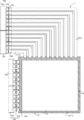
- FIG. 2 is a cross-sectional view taken along the line AA of the radiation imaging apparatus shown in FIG.
- FIG. 2 is a plan view showing an example of a state in which the folded flexible cable in FIG. 2 is unfolded without being folded.
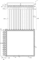
- Another example of the radiation imaging apparatus of the first embodiment is a plan view of the sensor substrate as viewed from the second side of the base material.
- FIG. 5 is a cross-sectional view taken along the line AA of the radiation imaging apparatus shown in FIG. FIG.
- FIG. 5 is a plan view showing an example of a state in which the flexible cable in the radiation imaging apparatus of Modification 1-1 is unfolded without being folded back.
- FIG. 5 is a plan view of the radiation imaging apparatus of Modification 1-1 as viewed from the second surface side of the base material. It is a top view which shows the other example of the state which expanded the flexible cable in the radiation image taking apparatus of the modification 1-1 without folding back. It is a top view which is seen from the 2nd surface side of the base material as an example of the radiation imaging apparatus of the modification 1-2. It is a top view which is seen from the 2nd surface side of the base material as an example of the radiation imaging apparatus of the modification 1-3.
- FIG. 5 is a plan view showing an example of a state in which the flexible cable in the radiation imaging apparatus of Modification 1-1 is unfolded without being folded back.
- FIG. 5 is a plan view of the radiation imaging apparatus of Modification 1-1 as viewed from the second surface side of the base material. It is a top view which shows
- FIG. 5 is a plan view of an example of the radiation imaging apparatus of the second embodiment as viewed from the second surface side of the base material. It is a top view which looked at another example of the radiation imaging apparatus of 2nd Embodiment from the 2nd surface side of the base material. It is a top view which shows an example of a relay board.
- An example of the radiation imaging apparatus of the modified example 2-1-1 is a plan view of the base material as viewed from the second surface side. It is a figure for demonstrating an example of bending of the 2nd relay part of the modification 2-1-1.
- An example of the radiation imaging apparatus of the modified example 2-1-1 is a plan view of the base material as viewed from the second surface side.
- An example of the radiation imaging apparatus of the modified example 2-1-2 is a plan view seen from the second surface side of the base material. It is a figure for demonstrating an example of the connection between the 2nd relay part and the 3rd relay part 313 of the modification 2-1-2. It is a figure for demonstrating another example of the connection between the 2nd relay part and the 3rd relay part 313 of the modification 2-1-2.
- FIG. 5 is a plan view of an example of the radiation imaging apparatus of Modification 2 as viewed from the second surface side of the base material. It is a top view of another example of the radiation imaging apparatus of modified example 2-2-1 seen from the second surface side of a base material.
- An example of the radiation imaging apparatus of the modified example 2-2-2 is a plan view seen from the first surface side of the base material.
- FIG. 5 is a plan view of the radiation imaging apparatus of the modified example 2-2-2 as viewed from the second surface side of the base material. It is a top view of another example of the radiation image taking apparatus of the modification 2 seen from the 2nd surface side of the base material.
- FIG. 5 is a plan view of an example of the radiation imaging apparatus of the third embodiment as viewed from the second surface side of the base material. It is a top view which looked at the other example of the radiation imaging apparatus of 2nd Embodiment from the 2nd surface side of the base material.
- FIG. 5 is a plan view of another example of the radiation imaging apparatus of the embodiment as viewed from the second surface side of the base material. It is sectional drawing of an example of the radiation imaging apparatus of embodiment which is housed in a housing. It is sectional drawing of another example of the radiation imaging apparatus of embodiment which is housed in a housing. It is sectional drawing of another example of the radiation imaging apparatus of embodiment which is housed in a housing.
- the radiation detector of the present embodiment has a function of detecting radiation transmitted through a subject and outputting image information representing a radiation image of the subject.
- the radiation detector of the present embodiment includes a sensor substrate and a conversion layer that converts radiation into light (see FIG. 2, sensor substrate 12 and conversion layer 14 of the radiation detector 10).
- the radiation imaging apparatus of the present embodiment will be described when the radiation detector is applied to an ISS (Irradiation Side Sampling) type radiation detector in which radiation R is irradiated from the sensor substrate side.
- ISS Immuno Service Side Sampling
- FIG. 1 is a block diagram showing an example of a configuration of a main part of an electrical system in the radiation imaging apparatus of the present embodiment.
- the radiation imaging device 1 of the present embodiment includes a radiation detector 10, a control unit 100, a drive unit 102, a signal processing unit 104, an image memory 106, and a power supply unit 108.
- the radiation detector 10 includes a sensor substrate 12 and a conversion layer (see FIG. 2) that converts radiation into light.
- the sensor substrate 12 includes a flexible base material 11 and a plurality of pixels 30 provided on the first surface 11A of the base material 11. In the following, the plurality of pixels 30 may be simply referred to as “pixel 30”.
- each pixel 30 of the present embodiment has a sensor unit 34 that generates and accumulates electric charges according to the light converted by the conversion layer, and a switching element 32 that reads out the electric charges accumulated by the sensor unit 34.
- a thin film transistor TFT: Thin Film Transistor
- the switching element 32 will be referred to as "TFT32".
- the sensor unit 34 and the TFT 32 are formed, and a layer in which the pixels 30 are formed on the first surface 11A of the base material 11 is provided as a flattened layer.
- the pixel 30 corresponds to the pixel region 35 of the sensor substrate 12 in one direction (scanning wiring direction corresponding to the horizontal direction in FIG. 1, hereinafter also referred to as “row direction”) and an intersecting direction with respect to the row direction (corresponding to the vertical direction in FIG. 1). It is arranged in a two-dimensional manner along the signal wiring direction (hereinafter also referred to as "row direction").
- row direction the arrangement of the pixels 30 is shown in a simplified manner. For example, 1024 pixels ⁇ 1024 pixels 30 are arranged in the row direction and the column direction.
- the radiation detector 10 is provided with a plurality of scanning wires 38 for controlling the switching state (on and off) of the TFT 32, which are provided for each row of the pixel 30, and for each column of the pixel 30.
- a plurality of signal wirings 36 from which the electric charge accumulated in the sensor unit 34 is read out are provided so as to intersect each other.
- Each of the plurality of scanning wires 38 is connected to the drive unit 102 via the flexible cable 206 (see FIG. 2) to drive the TFT 32 output from the drive unit 102 to control the switching state.
- a drive signal flows through each of the plurality of scanning wires 38.
- each of the plurality of signal wirings 36 is connected to the signal processing unit 104 via the flexible cable 406 (see FIG. 2), so that the electric charge read from each pixel 30 is signaled as an electric signal. It is output to the processing unit 104.
- the signal processing unit 104 generates and outputs image data corresponding to the input electric signal.
- a control unit 100 which will be described later, is connected to the signal processing unit 104, and the image data output from the signal processing unit 104 is sequentially output to the control unit 100.
- An image memory 106 is connected to the control unit 100, and image data sequentially output from the signal processing unit 104 is sequentially stored in the image memory 106 under the control of the control unit 100.
- the image memory 106 has a storage capacity capable of storing a predetermined number of image data, and each time a radiographic image is taken, the image data obtained by the taking is sequentially stored in the image memory 106.
- the control unit 100 includes a CPU (Central Processing Unit) 100A, a memory 100B including a ROM (Read Only Memory) and a RAM (Random Access Memory), and a non-volatile storage unit 100C such as a flash memory.
- a CPU Central Processing Unit
- a memory 100B including a ROM (Read Only Memory) and a RAM (Random Access Memory)
- a non-volatile storage unit 100C such as a flash memory.
- An example of the control unit 100 is a microcomputer or the like.
- the control unit 100 controls the overall operation of the radiographic imaging apparatus 1.
- the image memory 106, the control unit 100, and the like are formed on the control board 110.
- a common wiring 39 is provided in the wiring direction of the signal wiring 36 in order to apply a bias voltage to each pixel 30.
- a bias voltage is applied to each pixel 30 from the bias power supply by connecting the common wiring 39 to an external bias power supply (not shown) of the sensor board 12 via a terminal (not shown).
- the power supply unit 108 supplies electric power to various elements and circuits such as the control unit 100, the drive unit 102, the signal processing unit 104, the image memory 106, and the power supply unit 108.
- various elements and circuits such as the control unit 100, the drive unit 102, the signal processing unit 104, the image memory 106, and the power supply unit 108.
- the wiring connecting the power supply unit 108 with various elements and various circuits is omitted.
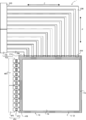
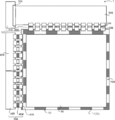
- FIG. 2 is a plan view of the radiation imaging apparatus 1 of the present embodiment as viewed from the first surface 11A side of the base material 11.
- FIG. 3 is a sectional view taken along line AA of the radiation imaging apparatus 1 in FIG.
- FIG. 4 shows an example of a state in which the flexible cable 206 folded back in FIG. 2 is unfolded without being folded back.
- the first surface 11A of the base material 11 is provided with a pixel region 35 provided with the above-mentioned pixel 30.
- the base material 11 is a resin sheet that has flexibility and contains, for example, a plastic such as PI (PolyImide: polyimide).
- the thickness of the base material 11 is such that the desired flexibility can be obtained according to the hardness of the material, the size of the sensor substrate 12 (the area of the first surface 11A or the second surface 11B), and the like. Good.
- As an example of having flexibility in the case of a rectangular base material 11 alone, with one side of the base material 11 fixed, gravity due to the weight of the base material 11 at a position 10 cm away from the fixed side The base material 11 hangs down by 2 mm or more (it becomes lower than the height of the fixed side).
- a thickness of 5 ⁇ m to 125 ⁇ m may be used, and a thickness of 20 ⁇ m to 50 ⁇ m is more preferable.
- the base material 11 has a property that can withstand the production of the pixel 30, and in the present embodiment, it has a property that can withstand the production of an amorphous silicon TFT (a-Si TFT).
- a-Si TFT amorphous silicon TFT
- the coefficient of thermal expansion (CTE) at 300 ° C. to 400 ° C. is about the same as that of an amorphous silicon (Si) wafer (for example, ⁇ 5 ppm / K). It is preferable to have.
- the coefficient of thermal expansion of the base material 11 at 300 ° C. to 400 ° C. is preferably 20 ppm / K or less.
- the heat shrinkage rate of the base material 11 it is preferable that the heat shrinkage rate at 400 ° C.
- the elastic modulus of the base material 11 does not have a transition point possessed by a general PI in the temperature range between 300 ° C. and 400 ° C., and the elastic modulus at 500 ° C. is preferably 1 GPa or more.
- the base material 11 of the present embodiment has a fine particle layer containing inorganic fine particles having an average particle diameter of 0.05 ⁇ m or more and 2.5 ⁇ m or less and absorbing backscattered rays in order to suppress backscattered rays by itself. It is preferable to have.
- inorganic fine particles in the case of the resinous base material 11, it is preferable to use an inorganic material having an atomic number larger than that of the atoms constituting the organic material which is the base material 11 and having an atomic number of 30 or less.
- Such fine particles include SiO 2 , which is an oxide of Si having an atomic number of 14, MgO, which is an oxide of Mg having an atomic number of 12, and Al 2 , which is an oxide of Al having an atomic number of 13. Examples thereof include O 3 and TiO 2 , which is an oxide of Ti having an atomic number of 22.
- Specific examples of the resin sheet having such characteristics include XENOMAX (registered trademark).
- the thickness in the present embodiment was measured using a micrometer.
- the coefficient of thermal expansion was measured according to JIS K7197: 1991. For the measurement, test pieces were cut out from the main surface of the base material 11 at different angles of 15 degrees, the coefficient of thermal expansion was measured for each of the cut out test pieces, and the highest value was taken as the coefficient of thermal expansion of the base material 11. ..
- the coefficient of thermal expansion is measured at intervals of 10 ° C. from -50 ° C to 450 ° C in each of the MD (Machine Direction) direction and the TD (Transverse Direction) direction, and (ppm / ° C) is converted to (ppm / K). did.
- a TMA4000S device manufactured by MAC Science Co., Ltd. was used, and the sample length was 10 mm, the sample width was 2 mm, the initial load was 34.5 g / mm 2 , the heating rate was 5 ° C / min, and the atmosphere was adjusted. Argon was used.
- the base material 11 having the desired flexibility is not limited to a resin sheet or the like.
- the base material 11 may be a glass substrate or the like having a relatively thin thickness.
- the base material 11 is a glass substrate, in general, when the size of one side is about 43 cm, the thickness is 0.3 mm or less because it has flexibility if the thickness is 0.3 mm or less. Any glass substrate may be desired.
- a conversion layer 14 is provided on the pixel region 35 of the present embodiment.
- the conversion layer 14 is provided on a part of the first surface 11A of the base material 11 including the pixel region 35.
- the conversion layer 14 of the present embodiment is not provided on the outer peripheral region of the first surface 11A of the base material 11.
- the term "upper" when used in the structure of the radiation detector 10, it means that the radiation detector 10 is above in the positional relationship with respect to the sensor substrate 12 side.
- the conversion layer 14 is provided on the sensor substrate 12.
- a scintillator containing CsI (cesium iodide) is used as an example of the conversion layer 14.
- CsI Tl (cesium iodide added with thallium)
- CsI Na (cesium iodide added with sodium) having an emission spectrum of 400 nm to 700 nm during X-ray irradiation. It is preferable to include it.
- the emission peak wavelength of CsI: Tl in the visible light region is 565 nm.
- the conversion layer 14 is a strip-shaped columnar crystal (strip-shaped columnar crystal) directly on the sensor substrate 12 by a vapor deposition method such as a vacuum deposition method, a sputtering method, and a CVD (Chemical Vapor Deposition) method. It is formed as (not shown).
- a vapor deposition method such as a vacuum deposition method, a sputtering method, and a CVD (Chemical Vapor Deposition) method. It is formed as (not shown).
- a method for forming the conversion layer 14 for example, when CsI: Tl is used as the conversion layer 14, CsI: Tl is heated by a heating means such as a resistance heating type pot in an environment of a vacuum degree of 0.01 Pa to 10 Pa.
- a vacuum vapor deposition method is used in which CsI: Tl is deposited on the sensor substrate 12 by vaporizing the sensor substrate 12 at room temperature (20 ° C.) to 300 ° C.
- the thickness of the conversion layer 14 is preferably 100 ⁇ m to 800 ⁇ m.
- the conversion layer 14 of the present embodiment is formed by the vapor phase deposition method, as shown in FIG. 3, the outer peripheral region of the conversion layer 14 becomes thicker toward the outside as a whole. It has a tendency to become thinner, and therefore has a slope that becomes thinner toward the outside.
- the thickness of the conversion layer 14 becomes thinner toward the outer periphery a form having a certain inclination and gradually becoming thinner is illustrated, but the present invention is not limited to this form, for example. , The thickness may change stepwise.
- the radiation detector 10 of the present embodiment includes an adhesive layer 40, a reflective layer 42, an adhesive layer 44, and a protective layer 46.
- the direction in which the base material 11, the pixels 30, and the conversion layer 14 are arranged is referred to as a stacking direction (see FIG. 3, stacking direction P).
- the conversion layer 14 side in the stacking direction P in the radiation detector 10 may be referred to as "upper", and the sensor substrate 12 side may be referred to as "lower".
- the adhesive layer 40 and the reflective layer 42 are provided on the entire conversion layer 14. Further, the adhesive layer 40 and the reflective layer 42 are not directly provided on the sensor substrate 12.
- the adhesive layer 40 of the present embodiment is a light-transmitting layer, and examples of the material of the adhesive layer 40 include acrylic adhesives, hot melt adhesives, and silicone adhesives.
- acrylic pressure-sensitive adhesive include urethane acrylate, acrylic resin acrylate, and epoxy acrylate.
- hot melt adhesive include EVA (ethylene / vinyl acetate copolymer resin), EAA (ethylene / acrylic acid copolymer resin), EEA (ethylene-ethylacrylate copolymer resin), and EMMA (ethylene-methacryl).
- Thermoplastics such as methyl acid copolymer) can be mentioned.
- MTF Modulation Transfer Function
- DQE Detective Quantum Efficiency
- the thickness of the adhesive layer 40 is made too thin, including the case where the adhesive layer 40 is not provided, a minute air layer may be formed between the conversion layer 14 and the reflective layer 42. In this case, the light directed from the conversion layer 14 to the reflection layer 42 is repeatedly reflected between the air layer and the conversion layer 14 and between the air layer and the reflection layer 42. If the light is attenuated by the multiple reflections, the sensitivity of the radiation detector 10 decreases. When the thickness of the adhesive layer 40 exceeds 7 ⁇ m, the degree of decrease in DQE becomes larger than when the adhesive layer 40 is not provided (when the thickness is 0 ⁇ m). Further, when the thickness of the adhesive layer 40 is less than 2 ⁇ m, the sensitivity of the radiation detector 10 decreases. Therefore, in the present embodiment, the thickness of the adhesive layer 40 is set to 2 ⁇ m or more and 7 ⁇ m or less. Although it depends on the material, the refractive index of the adhesive layer 40 is about 1.5.
- the adhesive layer 40 has a function of fixing the reflective layer 42 to the conversion layer 14, but if the thickness of the adhesive layer 40 is 2 ⁇ m or more, the reflective layer 42 is in-plane (thick) with respect to the conversion layer 14. A sufficient effect of suppressing deviation in the direction intersecting the vertical direction can be obtained.
- the reflective layer 42 is provided on the adhesive layer 40 and covers the entire upper surface of the adhesive layer 40 itself.
- the reflective layer 42 has a function of reflecting the light converted by the conversion layer 14.
- the material of the reflective layer 42 those using an organic material are preferable, and for example, white PET (Polyethylene Terephthalate), TiO 2 , Al 2 O 3 , foamed white PET, polyester-based highly reflective sheet, and specular reflective aluminum. It is preferable to use at least one of the above as a material. In particular, from the viewpoint of reflectance, those using white PET as a material are preferable.
- the white PET is obtained by adding a white pigment such as TiO 2 or barium sulfate to PET.
- the polyester-based high-reflection sheet is a sheet (film) having a multilayer structure in which a plurality of thin polyester sheets are stacked.
- the foamed white PET is a white PET having a porous surface.
- the thickness of the reflective layer 42 is 10 ⁇ m or more and 40 ⁇ m or less.
- the thickness of the reflective layer 42 is increased, the step between the upper surface of the outer peripheral portion of the reflective layer 42 and the upper surface of the conversion layer 14 becomes large, and at least one of the adhesive layer 44 and the protective layer 46 may be lifted. ..
- the thickness of the reflective layer 42 is increased, it becomes so-called stiff, so that it may be difficult to bend along the inclination of the peripheral edge portion of the conversion layer 14, which makes it difficult to process. Therefore, from these viewpoints, in the radiation detector 10 of the present embodiment, when white PET is used as the material of the reflective layer 42, the thickness of the reflective layer 42 is set to 40 ⁇ m or less as described above.
- the thinner the reflective layer 42 the lower the reflectance.
- the image quality of the radiation image obtained by the radiation detector 10 also tends to decrease. Therefore, from the viewpoint of the image quality of the radiation image obtained by the radiation detector 10, it is preferable to set the lower limit of the thickness of the reflection layer 42 in consideration of a desired reflectance (for example, 80%).
- a desired reflectance for example, 80%.
- the thickness of the reflection layer 42 is 10 ⁇ m or more as described above.
- the adhesive layer 44 is provided from above the region near the outer peripheral portion of the conversion layer 14 on the sensor substrate 12 to the region covering the end portion of the reflective layer 42.
- the adhesive layer 44 covering the entire conversion layer 14 provided with the adhesive layer 40 and the reflective layer 42 is directly fixed (adhesive) to the surface of the sensor substrate 12.
- the adhesive layer 44 has a function of fixing the reflective layer 42 to the sensor substrate 12 and the conversion layer 14.
- the adhesive layer 44 has a function of fixing the protective layer 46.
- Examples of the material of the adhesive layer 44 include the same materials as those of the adhesive layer 40. In the present embodiment, the adhesive force of the adhesive layer 44 is stronger than the adhesive force of the adhesive layer 40.
- the protective layer 46 is provided on the adhesive layer 44 as an example, and the protective layer 46 of the present embodiment is in a state where the upper surface is covered with the adhesive layer 40 and the reflective layer 42. It covers the entire upper surface of the adhesive layer 44 that covers the conversion layer 14.
- the protective layer 46 has a function of protecting the conversion layer 14 from moisture such as moisture. Further, the protective layer 46 has a function of fixing the reflective layer 42 to the sensor substrate 12 and the conversion layer 14 together with the adhesive layer 44.
- the material of the protective layer 46 examples include an organic film, for example, PET, PPS (PolyPhenylene Sulfide: polyphenylene sulfide), OPP (Oriented PolyPropylene: biaxially stretched polypropylene film), PEN (PolyEthylene Naphthalate). , PI and the like.
- a laminated film of a resin film and a metal film may be used as the protective layer 46.
- the laminated film of the resin film and the metal film examples include an Alpet (registered trademark) sheet in which aluminum is laminated by adhering aluminum foil to an insulating sheet (film) such as polyethylene terephthalate. ..
- a flexible cable 406 is electrically attached to the first surface 11A of the base material 11 of the sensor substrate 12 via a terminal (not shown) such as an anisotropic conductive film. It is connected.
- a terminal such as an anisotropic conductive film.
- one end of a plurality of (12 in FIG. 4) flexible cables 406 is thermocompression bonded to the sensor substrate 12.
- the flexible cable 406 has a function of connecting the signal processing unit 104 and the signal wiring 36 (see FIG. 1).
- a plurality of signal lines (not shown) included in the flexible cable 406 are connected to the signal wiring 36 (see FIG. 1) by thermocompression bonding to the sensor substrate 12.
- the flexible cable 406 of the present embodiment is an example of the first cable of the present disclosure.
- the other end of the flexible cable 406 is thermocompression bonded to the signal processing board 400.
- the flexible cable 406 is connected to one signal processing board 400.
- a plurality of signal lines (not shown) included in the flexible cable 406 are thermocompression-bonded to the signal processing board 400 to be connected to circuits, elements, and the like (not shown) mounted on the signal processing board 400.
- the signal processing board 400 of this embodiment is a flexible PCB (Printed Circuit Board) board, which is a so-called flexible board.
- the circuit components (not shown) mounted on the signal processing board 400 are components mainly used for processing analog signals (hereinafter, referred to as “analog components”). Specific examples of analog components include charge amplifiers, analog-to-digital converters (ADCs), digital-to-analog converters (DACs), power supply ICs, and the like. Further, the circuit component of the present embodiment also includes a coil around a power supply having a relatively large component size and a large-capacity capacitor for smoothing.
- the signal processing substrate 400 does not necessarily have to be a flexible substrate, may be a non-flexible rigid substrate, or may use a rigid flexible substrate.
- the flexible cable 406 is equipped with a signal processing IC (Integrated Circuit) 404.
- the signal processing IC 404 is connected to a plurality of signal lines (not shown) included in the flexible cable 406.
- the signal processing unit 104 is realized by the signal processing board 400 and the signal processing IC 404 mounted on the flexible cable 406.
- the signal processing IC 404 is an IC that includes a circuit different from the analog components mounted on the signal processing board 400 among various circuits and elements that realize the signal processing unit 104.
- the signal processing IC 404 of the present embodiment is an example of the signal processing circuit of the present disclosure.
- the flexible cable 206 is anisotropic on the side of the first surface 11A of the base material 11 of the sensor substrate 12 that intersects the side to which the flexible cable 406 is connected. It is electrically connected via a terminal (not shown) such as a conductive film.
- one end of a plurality of flexible cables 206 is thermocompression bonded to the sensor substrate 12.
- the flexible cable 206 has a function of connecting the drive unit 102 and the scanning wiring 38 (see FIG. 1).
- a plurality of signal lines (not shown) included in the flexible cable 206 are connected to the scanning wiring 38 (see FIG. 1) by thermocompression bonding to the sensor substrate 12.
- the flexible cable 206 of the present embodiment is an example of the second cable of the present disclosure.
- the other end of the flexible cable 206 is thermocompression bonded to the drive board 200.
- the flexible cable 206 is thermocompression bonded to the drive board 200.
- six flexible cables 206 are connected to one drive board 200.
- a plurality of signal lines (not shown) included in the flexible cable 206 are thermocompression-bonded to the drive board 200 to be connected to circuits, elements, and the like (not shown) mounted on the drive board 200.
- the 200 of the present embodiment is a flexible PCB (Printed Circuit Board) board, which is a so-called flexible board.
- the circuit parts (not shown) mounted on the drive board 200 are parts mainly used for processing digital signals (hereinafter, referred to as “digital parts”).
- Digital components tend to have a relatively smaller area (size) than analog components, which will be described later. Specific examples of digital components include digital buffers, bypass capacitors, pull-up / pull-down resistors, damping resistors, EMC (Electro Magnetic Compatibility) countermeasure chip components, power supply ICs, and the like.
- the drive substrate 200 does not necessarily have to be a flexible substrate, may be a non-flexible rigid substrate, or may use a rigid flexible substrate.
- the flexible cable 206 is equipped with a drive IC 204 at a position near the sensor board 12.
- the drive IC 204 is connected to a plurality of signal lines (not shown) included in the flexible cable 206.
- the drive unit 102 is realized by the drive board 200 and the drive IC 204 mounted on the flexible cable 206.
- the drive IC 204 is an IC that includes a circuit different from the digital components mounted on the drive board 200 among various circuits and elements that realize the drive unit 102.
- the drive IC 204 of the present embodiment is an example of the drive circuit of the present disclosure.
- the flexible cable 206 of the present embodiment has a shape bent from the direction connected to the side of the sensor substrate 12 in the direction intersecting the side to which the flexible cable 206 is connected.
- the flexible cable 206 includes one end connected to the sensor substrate 12 and extends in the first direction ⁇ intersecting the direction of the side to which the flexible cable 206 of the sensor substrate 12 is connected. It has a portion and a portion that includes the other end connected to the drive substrate 200 and extends in a second direction ⁇ that intersects the first direction.
- each of the flexible cables 206 shows an L-shape bent by about 90 degrees.
- the flexible cable 206 is formed from the side of the first surface 11A of the base material 11 of the sensor substrate 12. Specifically, it passes over the conversion layer 14 and is connected to the drive board 200.
- the flexible cable 206 is folded back to the side opposite to the side where the radiation detector 10 is irradiated with radiation.
- the side opposite to the side irradiated with radiation is a flexible cable. 206 passes.
- the flexible cable 206 passes through the conversion layer 14 side.
- the flexible cable 206 is a sensor substrate as shown in FIG. 6 which is a cross-sectional view taken along the line AA of FIGS. 5 and 5. It passes through the second surface 11B side of the base material 11 of 12.
- the radiographic imaging apparatus 1 of the present embodiment may be in the form shown in the following modifications 1-1 to 1-3, for example.
- the flexible cable 206 of the radiographic imaging apparatus 1 may have a straight shape extending in a straight line.
- FIG. 8 shows an example in which the radiation imaging apparatus 1 is of the PSS system and the flexible cable 206 is folded back toward the second surface 11B of the base material 11 on the sensor substrate 12. As shown in FIG. 8, the flexible cable 206 is bent in a direction of folding back with respect to the extending direction of the flexible cable 206, and further bent in a direction intersecting the extending direction of the flexible cable 206.
- the plurality of flexible cables 206 connected to the sensor board 12 all have the same shape. Therefore, the radioimaging apparatus 1 can be easily manufactured, and the manufacturing cost can be suppressed.
- the drive IC 204 is mounted on the side of the flexible cable 206 close to the drive board 200.
- the position where the drive IC 204 is mounted is not limited.
- the drive IC 204 may be mounted on the drive board 200.
- the specific position for mounting the drive IC 204 for example, the influence of noise due to the drive IC 204, the specifications of the radiation imaging device 1, the size of the housing 120 (see FIG. 29) for accommodating the radiation detector 10, etc. The position may be adjusted accordingly.
- the flexible cable 206 of the radiation imaging apparatus 1 may be in a form in which the number connected to the drive board 200 is smaller than the number connected to the sensor board 12.
- the ends of the relatively wide flexible cable 206 connected to the drive board 200 are divided into six, and each of the six divided ends is connected to the sensor board 12. ing.
- a drive IC 204 is mounted on each of the six ends connected to the sensor board 12 of the flexible cable 206.
- a plurality of (six in FIG. 10) flexible cables 206 in the flexible cable 206 are integrated into one, and the drive board 200 It differs in that it is connected to.
- the flexible cables 206 can be easily handled by the radiation imaging apparatus 1 of this modified example.
- the flexible cable 206 of the radiation imaging apparatus 1 is connected to the scanning wiring 38 of the sensor substrate 12 via the connector 300 instead of being connected to the sensor substrate 12 by thermocompression bonding. It may be in the form. Further, the flexible cable 206 may be connected to the drive board 200 via a connector 302 instead of being connected to the drive board 200 by thermocompression bonding. Examples of such connectors 300 and 302 include a ZIF (Zero Insertion Force) structure connector and a Non-ZIF structure connector.
- ZIF Zero Insertion Force
- the flexible cable 206 connected to the sensor substrate 12 is connected to the side of the first surface 11A of the base material 11 or the first surface 11A of the base material 11. It passes through the side of the second surface 11B on the opposite side and is electrically connected to the drive board 200.
- the drive board 200 can be arranged on the same side of the sensor board 12 as the signal processing board 400.
- the portion corresponding to the sensor substrate 12 can be thinned.
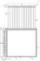
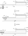
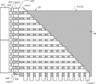
- FIG. 12 is a plan view of the radiation imaging apparatus 1 of the present embodiment in a state where the flexible cable 206 is not folded back, as viewed from the first surface 11A side of the base material 11.
- the flexible cable 206 of the first embodiment has the first embodiment in that the end opposite to the end connected to the sensor board 12 is connected to the relay board 310 instead of the drive board 200. It is different from the radiation imaging device 1 (see FIG. 4).
- the relay board 310 and the flexible cable 206 are connected by thermocompression bonding. Further, the relay board 310 and the drive board 200 are connected by a connector 304.
- the radiation imaging apparatus 1 may use two relay boards 310 (310A and 310B).
- the radiation imaging apparatus 1 may use two relay boards 310 (310A and 310B).
- six flexible cables 206 are connected to the relay board 310A in order from the side closest to the signal processing board 400, and the relay board 310A and the drive board 200 are connected by the connector 304A.
- six flexible cables 206 are connected to the relay board 310B in order from the far side to the signal processing board 400, and the relay board 310B and the drive board 200 are connected by the connector 304B.
- the relay board 310 of this embodiment includes three parts, a connecting part 314, a folded part 316, and a relay part 318.
- connection unit 314 is a multi-layer FPC (Flexible printed circuits), and as an example, in the present embodiment, a 4-layer FPC is used.
- the connection portion 314 is provided with a thermocompression bonding pattern 315 in which the flexible cable 206 is thermocompression bonded.
- the folded portion 316 is a portion for folding the relay substrate 310 toward the first surface 11A side or the second surface 11B side of the base material 11, and is thinner than the connecting portion 314 and the relay portion 318. ing.
- the thickness is reduced to 1/4 (1/4) as compared with each of the connecting portion 314 and the relay portion 318.
- the relay unit 318 is a portion for relaying the connection between the flexible cable 206 and the drive board 200, and is mounted on the drive board 200 on the side where the connector 304 connected to the drive board 200 is provided.
- a component mounting area 319 on which the above digital components are mounted is provided.
- the relay unit 318 is a multi-layer FPC, and as an example, in the present embodiment, a 4-layer FPC is used.
- a flexible (flexible) substrate is used as the relay board 310, but the present embodiment is not limited to this, and the relay board 310 relays the flexible cable 206 and the drive board 200. May use a rigid substrate or a rigid flexible substrate.
- the radiation imaging device 1 of the present embodiment may be in the form shown in the following modified examples 2-1-1 to 2-2-2, for example.
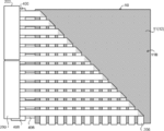
- FIG. 15 shows a modified example of the relay boards 310A and 310B.
- FIG. 15 shows a plan view of the radiation imaging apparatus 1 of this modified example as viewed from the second surface 11B side of the base material 11.
- the description of the drive board 200, the signal processing board 400, and the like is omitted in order to avoid complicating the drawings.
- the relay board 310A in the radiation imaging apparatus 1 of this modification is the drive board 200 on the side where the connector 304 connected to the drive board 200 is provided.
- a component mounting area 319A and a connector 304A on which the digital components mounted in the vehicle are mounted are provided.
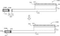
- the relay board 310B includes a first relay unit 311 electrically connected to the flexible cable 206 and a second relay unit 312.
- the second relay unit 312 extends in a direction intersecting with the long side 312A extending along the side 12A to which the flexible cable 206 of the sensor board 12 is electrically connected and the long side 312A extending, and also with the drive board 200. It shows an L-shape having a short side 312B that is electrically connected.
- the short side 312B is provided with a component mounting area 319B and a connector 304B on which the digital components mounted on the drive board 200 are mounted.
- the long side 312A and the short side 312B of the second relay portion 312 intersect with each other by the bent portion 320, and the short side 312B is bent at the bent portion 320 in the direction along the long side 312A.
- the bending of the second relay unit 312 will be described with reference to FIG. First, the short side 312B is bent so as to overlap the long side 312A by the valley folding line 320V of the bent portion 320. Next, the short side 312B is bent in the direction in which the tip is separated from the long side 312A by the mountain folding line 320M of the bent portion 320.
- the overlapping region on which the second relay portion 312 is superimposed by bending the bent portion 320 is set to a position that does not overlap with the component mounting area 319B, and is set to a position that overlaps with the long side 312A.
- the length of the second relay portion 312 extending along the side 12A of the sensor substrate 12 becomes longer than the length of the long side 312A.
- FIG. 17 shows an example of a state in which the relay boards 310A and 310B are folded back toward the second surface 11B side of the base material 11 on the sensor board 12 in the radiation imaging device 1 of this modified example.
- the description of the drive board 200, the flexible cable 206, the signal processing board 400, and the like is omitted in order to avoid complicating the drawings.
- the bent portion 320 is located outside the sensor board 12, and the bent portion 320 and the sensor board 12 do not overlap. Further, the component mounting area 319B of the second relay unit 312 is also located outside the sensor board 12, and the component mounting area 319B and the sensor board 12 do not overlap.
- the length of the second relay portion 312 extending along the side 12A of the sensor substrate 12 is increased.
- the size (length) of the substrate constituting the relay substrate 310B can be suppressed, the manufacturing suitability can be improved, and the cost increases with the increase in size. Can be suppressed.
- the overlapping region generated by bending the bent portion 320 in the relay board 310B does not overlap with the sensor board 12, so that the radiation imaging device 1 corresponding to the sensor board 12
- the part can be made thinner.
- the direction in which the long side 312A and the short side 312B intersect is not limited to the form of this modification.
- an L-shaped form opposite to that of the present modification specifically, a form in which the short side 312B extends toward the first relay portion 311 may be used.
- the "L-shape" referred to in the relay board 310B is not limited to the form in which the long side 312A and the short side 312B intersect at a right angle, and also includes a form in which the long side 312A and the short side 312B intersect at a right angle.
- the method of bending the relay board 310B in the bent portion 320 is not limited.
- the above-mentioned valley folding line 320V may be used as a mountain folding line
- the mountain folding line 320M may be used as a valley folding line.
- the position of the overlapping region of the second relay portion 312 by bending the bent portion 320 is not limited as long as it does not overlap with the sensor substrate 12, but the position where the portion overlaps with the component mounting region 319B is small.
- a position that does not overlap with the component mounting area 319B is more preferable.
- FIG. 18 shows an example of a state in which the relay substrates 310A and 310B are folded back toward the second surface 11B of the substrate 11 on the sensor substrate 12 in the radiation imaging apparatus 1 of this modified example. Note that in FIG. 18, the description of the drive board 200, the flexible cable 206, the signal processing board 400, and the like is omitted in order to avoid complicating the drawings.
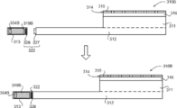
- the relay board 310B of this modified example has a first relay unit 311 electrically connected to the flexible cable 206, a second relay unit 312, and a third relay unit 313. And include.
- the second relay unit 312 extends along the side 12A to which the flexible cable 206 of the sensor board 12 is electrically connected.
- the third relay unit 313 is electrically connected to one end of the second relay unit 312 and the other end is electrically connected to the drive board 200.
- the third relay unit 313 is provided with a component mounting area 319B and a connector 304B on which the digital components mounted on the drive board 200 are mounted.
- the second relay unit 312 and the third relay are relayed by the connection unit 322 including the thermocompression bonding pattern 323 of the second relay unit 312 and the thermocompression bonding pattern 324 of the third relay unit 313.
- the connection unit 322 including the thermocompression bonding pattern 323 of the second relay unit 312 and the thermocompression bonding pattern 324 of the third relay unit 313.
- the second relay portion 312 and the third relay portion 313 are electrically connected.
- the top and bottom (front and back) of the thermocompression bonding pattern 323 of the second relay unit 312 and the thermocompression bonding pattern 324 of the third relay unit 313 are not limited.
- the thermocompression bonding pattern 323 is located on the upper (front) side in FIG. 19, and the second relay portion 312 and the third relay portion 313 are in a state where the thermocompression bonding pattern 324 is on the lower (back) side. Is thermocompression bonded.
- connection portion 322 is provided in a region that does not overlap with the sensor substrate 12. Further, the connection portion 322 of this modification is provided at a position that does not overlap with the signal processing IC 404.
- the relay board 310B includes the second relay section 312 and the third relay section 313 connected to the second relay section 312, the length extending along the side 12A of the sensor board 12 in the relay board 310B. Can be longer than the side 12A.
- the length of the second relay portion 312 extending along the side 12A of the sensor board 12 is about the length L1 of the side 12A or less than the length L1, the length of the relay board 310B along the side 12A. Can be made longer than the length L1 of the side 12A. Therefore, the drive board 200 can be arranged at a position that does not overlap with the sensor board 12. Further, according to this modification, since the size (length) of the substrate constituting the relay substrate 310B can be suppressed, the manufacturing suitability can be improved, and the cost increases with the increase in size. Can be suppressed.
- connection portion 322 since the connection portion 322 does not overlap with the sensor substrate 12, the portion of the radiation imaging device 1 corresponding to the sensor substrate 12 can be thinned.
- connection portion 322 is not limited to the form of this modification.
- An example of another form of the connecting portion 322 is shown in FIG.
- the connection unit 322 shown in FIG. 20 includes a connector connection pattern 327 provided in the second relay unit 312 and a connector 328 provided in the third relay unit 313.
- the connection unit 322 shown in FIG. 20 by connecting (inserting) the connector connection pattern 327 to the connector 328, the second relay unit 312 and the third relay unit 313 are electrically connected via the connector 328. ..
- the relay board 310B includes the second relay unit 312 and the third relay unit 313, and the connection unit 322 electrically connects the second relay unit 312 and the third relay unit 313.
- the present invention is not limited to this mode, and the relay board 310A may have the same form. That is, the relay board 310A has a form including the second relay section 312 and the third relay section 313, and the second relay section 312 and the third relay section 313 are electrically connected by the connection section 322, whereby the sensor board 12 The length of the relay board 310A along the side 12A may be longer than that of the second relay unit 312.
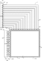
- the radiation imaging apparatus 1 may have a form in which the end of the flexible cable 206 is connected to the relay board 310C instead of the sensor board 12.
- the radiation imaging apparatus 1 of this modified example includes a plurality of relay boards 310C (12 in FIG. 21), and one end of each relay board 310C heats the flexible cable 206. It is connected by crimping, and the other end is connected to the sensor substrate 12 by thermocompression bonding.
- each of the relay boards 310C is bent about 90 degrees in the direction of the drive board 200 (signal processing board 400), similarly to the flexible cable 206 (see FIG. 4) of the first embodiment. It is L-shaped. Further, in the example shown in FIG. 22, each of the relay boards 310C has a straight shape extending in a straight line like the flexible cable 206 of the modified example 1-1 (see FIG. 7) of the first embodiment.
- the flexible cable 206 and the sensor substrate 12 may be connected by the relay substrate 310C as in the radiation imaging apparatus 1 of the modified example.
- the relay board 310 of the radiation imaging apparatus 1 may include a plurality of relay boards.
- FIG. 23 shows a plan view of the radiation imaging apparatus 1 in which the relay board 310C includes two relay boards, as viewed from the first surface 11A side of the base material 11.
- the relay board 310C of the radiation imaging apparatus 1 shown in FIG. 23 includes a first relay board 310C1 and a second relay board 310C2. One end of the first relay board 310C1 is electrically connected to the sensor board 12. One end of the second relay board 310C2 is electrically connected to the other end of the first relay board 310C1, and the other end is electrically connected to the flexible cable 206. As an example, in this modification, the second relay board 310C2, the first relay board 310C1, and each of the flexible cable 206 are electrically connected by thermocompression bonding.
- FIG. 24 shows an example of a state in which the relay board 310C is folded back toward the second surface 11B side of the base material 11 on the sensor board 12.
- the first relay board 310C1 is bent in a direction of folding back with respect to the extending direction of the first relay board 310C1, and further bent in a direction intersecting the extending direction of the first relay board 310C1. ing.
- connection unit 329 in which the first relay board 310C1 and the drive circuit unit 210 capacitor C2 are electrically connected is located outside the sensor board 12, and the connection unit 329 and the sensor board 12 are located outside the sensor board 12. Does not overlap.
- the relay board 310C includes the first relay board 310C1 and the second relay board 310C2
- the first relay board 310C1 and the second relay board 310C2 are respectively.
- the size (length) can be reduced.
- the size (length) of each of the first relay board 310C1 and the second relay board 310C2 can be made smaller (shorter) than the relay board 310C shown in FIG. 22.
- the relay board 310C can be configured by combining the relay boards having a small size. Therefore, according to the present modification, the manufacturing suitability can be improved, and the increase in cost due to the increase in size can be suppressed.
- connection portion 329 does not overlap with the sensor substrate 12
- the portion of the radiation imaging device 1 corresponding to the sensor substrate 12 can be made thinner.
- the position of the drive IC 204 on the front and back sides of the flexible cable 206 can be easily set to the same position as when the relay board 310C is not folded back.
- each of the first relay board 310C1 and the second relay board 310C2 is not limited to this modification, but as described above, it is preferable that the connection portion 329 has a length that does not overlap with the sensor board 12.
- the relay board 310C may be connected to the scanning wiring 38 of the sensor board 12 via the connector 306 instead of being connected to the sensor board 12 by thermocompression bonding. .. Further, the relay board 310C may be connected to the drive board 200 via the connector 308 instead of being connected to the drive board 200 by thermocompression bonding. Examples of such connectors 306 and 308 include a ZIF (Zero Insertion Force) structure connector and a Non-ZIF structure connector.
- ZIF Zero Insertion Force
- connection between the second relay board 310C2 and the first relay board 310C1 of the radiation imaging apparatus 1 shown in FIGS. 23 and 24 and the connection between the second relay board 310C2 and the flexible cable 206 are also performed by thermocompression bonding. Instead of being connected, it may be connected via a connector.
- the relay board 310 is not connected to the flexible cable 206 by thermocompression bonding. It may be connected via a connector.
- the relay board 310 instead of being connected to the drive board 200 by the connectors 304 (304A and 304B), it may be connected by thermocompression bonding.
- FIG. 26 and 27 show a plan view of the radiation imaging apparatus 1 of the present embodiment as viewed from the second surface 11B side of the base material 11.
- FIG. 26 shows an example of a form including the L-shaped flexible cable 206, similarly to the flexible cable 206 of the first embodiment (see FIG. 4).
- FIG. 27 shows an example of a form in which the flexible cable 206 having a straight shape is provided, similar to the flexible cable 206 (see FIG. 7) of the radiation imaging apparatus 1 of the modified example 1-1.
- the radiation imaging apparatus 1 of the present embodiment includes a shielding member 330 between the first surface 11A of the base material 11 (sensor substrate 12) and the flexible cable 206. ing. Further, the shielding member 330 of the present embodiment is also provided between the drive board 200 and the signal processing board 400, and between the drive IC 204 and the signal processing IC 404.
- the shielding member 330 is a member that shields at least one of electricity, magnetism, and radiation.
- Examples of the material of the shielding member 330 include copper and Alpet (registered trademark).
- the current flowing through the flexible cable 406 via the signal wiring 36 due to the electric charge read from the pixel 30 is generally a very small current on the order of several fA to several pA or the like.
- this current is converted into a voltage by a charge amplifier included in the signal processing board 400 and then A / D converted, it is a very small minute electric signal (hereinafter referred to as "read signal") of several tens of ⁇ V per bit. ).
- the potential of the drive signal flowing through the scanning wiring 38 via the flexible cable 206 is 20V to 40V, which is a very large voltage as compared with the read signal. Therefore, when the signal processing board 400 and the drive board 200 overlap or are arranged very close to each other, there is a concern that noise may be superimposed on the read signal due to the influence of electromagnetic induction by the drive signal on the flexible cable 406. There is.
- a shielding member 330 that shields at least one of electricity and magnetism is provided between the driving IC 204 and the signal processing IC 404 and between the driving substrate 200 and the signal processing substrate 400.
- the flexible cable 206 may generate backscattered rays, and the flexible cable 206 may be reflected in the radiation image generated by the radiation detector 10. Therefore, in the radiation imaging apparatus 1 of the present embodiment, the flexible cable 206 is reflected in the radiation image by providing a shielding member 330 that shields the radiation which is the backscattered rays between the flexible cable 206 and the sensor substrate 12. It is possible to suppress the crowding.
- the radiation imaging apparatus 1 of each of the above-described embodiments applies an electric charge generated in response to the light converted from the radiation to the pixel region 35 of the first surface 11A of the flexible base material 11.
- a sensor substrate 12 on which a plurality of pixels 30 to be accumulated are formed, and a conversion layer 14 for converting radiation into light provided on the first surface 11A of the substrate 11 are provided.
- the radiation imaging device 1 is provided on one side of a pair of sides of the sensor board 12 facing each other, and an electric signal corresponding to the charge accumulated in the plurality of pixels 30 of the sensor board 12 is input.
- One side of a pair of sides of the signal processing board 400 including at least a part of the circuits of the signal processing unit 104 that generates and outputs image data corresponding to the input electric signal, and the sensor board 12.
- At least a part of the circuit of the drive unit 102 provided on the other side and outputting the drive signal for outputting the charge accumulated from each of the plurality of pixels 30 of the sensor board 12 to each of the plurality of pixels 30.
- the drive board 200 including the above.
- one end of the radiation imaging device 1 is provided along one side of a pair of sides of the sensor board 12, and is electrically connected to the sensor board 12, and the other end is electrically connected to the signal processing board 400.
- the flexible cable 406 is provided along a side of a pair of sides of the sensor board 12 that intersects with one side, and is electrically connected to the sensor board 12 to form a first surface 11A of the base material 11.
- a flexible cable 206 is provided, which passes through the side or the side of the second surface 11B opposite to the first surface 11A of the base material 11, and the other end is electrically connected to the drive substrate 200.
- the flexible cable 206 connected to the sensor substrate 12 is located on the side of the first surface 11A of the base material 11 or the first of the base material 11. It passes through the side of the second surface 11B opposite to the surface 11A and is electrically connected to the drive board 200.
- the drive board 200 can be arranged on the side of the sensor board 12 on the same side as the signal processing board 400, or on the side opposite to the side to which the signal processing board 400 is connected.
- the portion of the radiation imaging device 1 corresponding to the sensor substrate 12 can be made thinner.
- the wiring provided in the sensor board 12 is Since the film thickness is relatively thin, about several hundred nm, high resistance is obtained even when the wiring length is short.
- the film thickness is about several ⁇ m to several tens of ⁇ m, which is 10 to 100 times or more the thickness of the above wiring. Therefore, the resistance can be low.
- the flexible cable 206 can be wired using copper having a resistivity lower than that of the wiring material in the sensor substrate 12, so-called wiring resistance can also be lowered.
- the end of the flexible cable 206 may be connected to the outer edge of the sensor substrate 12, and the flexible cable 206 is folded back, so that the radiation imaging device 1 is used. It is possible to suppress the increase in size. In particular, it is possible to prevent the area of the sensor substrate 12 of the radiographic imaging apparatus 1 from becoming large.
- the wiring provided in the sensor substrate 12 has a relatively thin film thickness of about several hundred nm. There is a concern that the scanning wiring 38 may be disconnected due to metal fatigue caused by vibration or the like.
- the film thickness of the wiring is about several ⁇ m to several tens of ⁇ m, and the reinforcing base material can be arranged. Moreover, since the sensor substrate 12 itself is not bent, the concern about disconnection is suppressed.
- the circuit components and the drive IC 204 mounted on the drive board 200 and the circuit components and the signal processing IC 404 mounted on the signal processing board 400 in the radiation imaging apparatus 1 of each of the above embodiments are shown in FIG. 28.
- the drive signal has a very large voltage as compared with the read signal, and the closer each of the drive board 200 and the drive IC 204 is to each of the signal processing board 400 and the signal processing IC 404, the more electromagnetically due to the drive signal. Due to the influence of the induction, there is a high concern that noise is superimposed on the read signal.
- the circuit components and the drive IC 204 mounted on the drive board 200 and the circuit components and the signal processing IC 404 mounted on the signal processing board 400 do not overlap. By doing so, it is possible to suppress the superimposition of the above noise on the read signal.
- the state in which the circuit components and the drive IC 204 mounted on the drive board 200 and the circuit components and the signal processing IC 404 mounted on the signal processing board 400 do not overlap is not limited to the form shown in FIG. 28.
- one of the drive board 200 and the drive IC 204 and the signal processing board 400 and the signal processing IC 404 may be arranged at a position close to the sensor board 12 and the other at a position away from the sensor board 12. Good.
- the noise can be suppressed by being superimposed on the read signal regardless of the specific form.
- all the circuits such as the drive IC 204 included in the drive unit 102 and all the circuits such as the signal processing IC 404 included in the signal processing unit 104 do not overlap. It is more preferable that it is in a state.
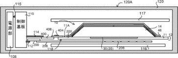
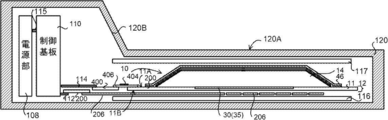
- the radiation detector 10 and the like of the radiation imaging device 1 of each of the above embodiments are used in a state of being housed in the housing 120 as shown in FIGS. 29 to 31.
- FIG. 29 shows a cross-sectional view of an example of the ISS type radiation imaging apparatus 1.
- the radiation detector 10, the power supply unit 108, and the control board 110 are provided side by side in the housing 120 in a direction intersecting the incident direction of the radiation.
- the radiation detector 10 is arranged in a state in which the first surface 11A side of the base material 11 on the sensor substrate 12 faces the irradiation surface 120A side of the housing 120 in which the radiation transmitted through the subject is irradiated.
- FIG. 30 shows a cross-sectional view of an example of the PSS type radiation imaging apparatus 1.
- a radiation detector 10 a power supply unit 108, and a control board 110 are provided side by side in the housing 120 in a direction intersecting the incident direction of radiation.
- the radiation detector 10 is arranged so that the second surface 11B side of the base material 11 on the sensor substrate 12 faces the irradiation surface 120A side of the housing 120 in which the radiation transmitted through the subject is irradiated.
- control board 110 and the drive board 200 are connected by a flexible cable 112. Further, the control board 110 and the signal processing board 400 are connected by a flexible cable 114.
- control board 110 is connected to the power supply unit 108 that supplies power to the image memory 106, the control unit 100, and the like formed on the control board 110 by the power supply line 115.
- a sheet 116 is further provided in the housing 120 of the radiation imaging apparatus 1 shown in FIGS. 29 and 30 on the side where the radiation transmitted through the radiation detector 10 is emitted.
- Examples of the sheet 116 include a copper sheet.
- the copper sheet is less likely to generate secondary radiation due to incident radiation, and therefore has a function of preventing scattering to the rear, that is, to the conversion layer 14 side. It is preferable that the sheet 116 covers at least the entire surface of the conversion layer 14 on the side where the radiation is emitted, and also covers the entire conversion layer 14.
- a protective layer 117 is further provided on the side where radiation is incident (the irradiation surface 120A side).
- a moisture-proof film such as an Alpet (registered trademark) sheet, a parylene (registered trademark) film, and an insulating sheet such as polyethylene terephthalate can be applied to the insulating sheet (film).
- the protective layer 117 has a moisture-proof function and an antistatic function for the pixel array 31. Therefore, the protective layer 117 preferably covers at least the entire surface of the pixel array 31 on the side where the radiation is incident, and preferably covers the entire surface of the sensor substrate 12 on the side where the radiation is incident.
- each of the power supply unit 108 and the control board 110 is often thicker than the radiation detector 10.
- the housing 120 in which the radiation detector 10 is provided is thicker than the thickness of the housing 120 in which each of the power supply unit 108 and the control board 110 is provided.
- the thickness of the portion may be thinner. In this way, when the thickness of the housing 120 in which the power supply unit 108 and the control board 110 are provided and the thickness of the housing 120 in which the radiation detector 10 is provided are different. If there is a step at the boundary between the two portions, there is a concern that the subject who comes into contact with the boundary 120B may feel uncomfortable. Therefore, it is preferable that the boundary 120B has an inclined shape.
- the material of the housing 120 is a portion of the housing 120 in which each of the power supply unit 108 and the control board 110 is provided and a portion of the housing 120 in which the radiation detector 10 is provided. It may be different. Further, for example, even if the portion of the housing 120 in which each of the power supply unit 108 and the control board 110 is provided and the portion of the housing 120 in which the radiation detector 10 is provided are configured as separate bodies. Good.
- the housing 120 is preferably made of a material having a low radiation R, particularly X-ray absorption rate, high rigidity, and a sufficiently high elastic modulus.
- the part of the body 120 corresponding to the irradiation surface 120A is made of a material having a low radiation R absorption rate, high rigidity, and a sufficiently high elastic modulus, and the other parts are parts corresponding to the irradiation surface 120A. It may be composed of a material different from the above, for example, a material having a lower elastic modulus than the portion of the irradiation surface 120A.
- the drive board 200 and the signal processing board 400 are provided on the same side of the sensor board 12, but the arrangement of the drive board 200 and the signal processing board 400 will be described. It is not limited to the form.
- the drive board 200 may be provided on the side of the sensor board 12 opposite to the side on which the signal processing board 400 is provided.
- both sides of the sensor board 12 facing each other are thicker than the sensor board 12 portion. It will be in a state of having.
- the flexible cable 206 since the flexible cable 206 only passes through the portion of the sensor substrate 12, the thickness of the radiographic imaging apparatus 1 can be reduced in the portion of the sensor substrate 12.
- the radiation imaging device 1 is not limited to each of the above embodiments, and may be, for example, a form in which the flexible cable 206 and the drive board 200 are connected via another flexible cable. In this case, since the flexible cable 206 remains short in the manufacturing process of the radiation imaging apparatus 1, the radiation detector 10 can be easily handled.
- the present invention is not limited to this, and for example, it may be a one-dimensional array or a honeycomb. It may be an array.
- the shape of the pixel 30 is not limited, and it may be a rectangle or a polygon such as a hexagon. Further, it goes without saying that the shape of the pixel array 31 (pixel region 35) is not limited.
- the position where the drive IC 204 and the flexible cable 406 are mounted is not limited to each of the above embodiments. That is, whether the drive IC 204 is mounted on the front or back of the flexible cable 206 and the specific mounting position are not limited to the above embodiments. Further, which of the front and back sides of the flexible cable 406 the signal processing IC 404 is executed and the specific mounting position are not limited to the above embodiments.
- the shape of the conversion layer 14 and the like are not limited to each of the above embodiments.
- the shape of the conversion layer 14 is rectangular like the shape of the pixel array 31 (pixel area 35) has been described, but the shape of the conversion layer 14 is the pixel array 31 (pixel area 35). It does not have to have the same shape as.
- the shape of the pixel array 31 (pixel region 35) is not rectangular, but may be, for example, another polygon or a circle.
- the configurations of the radiation imaging apparatus 1 and the radiation detector 10 and the like described in each of the above embodiments are examples, and it goes without saying that they can be changed depending on the situation within a range that does not deviate from the gist of the present invention. Nor.
- Radiation imaging device 10 Radiation detector 11 Base material, 11A 1st surface, 11B 2nd surface 12 Sensor substrate, 12A Side 14 Conversion layer 19 Laminated 30 pixels 31 Pixel array 32 Switching element (TFT) 34 Sensor unit 35 Pixel area 36 Signal wiring 38 Scanning wiring 39 Common wiring 40 Adhesive layer 42 Reflective layer 44 Adhesive layer 46 Protective layer 80 Gate electrode 100 Control unit, 100A CPU, 100B memory, 100C Storage unit 102 Drive unit 104 Signal processing unit 106 Image memory 108 Power supply 110 Control board 112, 114 Flexible cable 115 Power line 116 Sheet 117 Protective layer 120 Housing, 120A irradiation surface, 120B Boundary 200 Drive board 204 Drive IC 206, 406 Flexible cables 300, 302, 304, 304A, 304B, 306, 308 Connector 310, 310A, 310B, 310C Relay board, 310C1 First relay board, 310C2 Second relay board 311 First relay section 312 Second relay section , 312A Long side, 312B Short
Landscapes
- Health & Medical Sciences (AREA)
- Life Sciences & Earth Sciences (AREA)
- High Energy & Nuclear Physics (AREA)
- Molecular Biology (AREA)
- Physics & Mathematics (AREA)
- General Physics & Mathematics (AREA)
- Spectroscopy & Molecular Physics (AREA)
- Medical Informatics (AREA)
- Engineering & Computer Science (AREA)
- Pathology (AREA)
- Surgery (AREA)
- Optics & Photonics (AREA)
- Biophysics (AREA)
- Radiology & Medical Imaging (AREA)
- Biomedical Technology (AREA)
- Heart & Thoracic Surgery (AREA)
- Nuclear Medicine, Radiotherapy & Molecular Imaging (AREA)
- Animal Behavior & Ethology (AREA)
- General Health & Medical Sciences (AREA)
- Public Health (AREA)
- Veterinary Medicine (AREA)
- Measurement Of Radiation (AREA)
- Apparatus For Radiation Diagnosis (AREA)
- Toxicology (AREA)
Abstract
一端がセンサ基板の一対の辺における一方の辺に沿って設けられ、センサ基板と電気的に接続され、他端が信号処理基板に電気的に接続されるフレキシブルケーブルと、一端がセンサ基板の一対の辺における一方の辺と交差する辺に沿って設けられ、センサ基板と電気的に接続され、基材の第1の面の側、または基材の第1の面と反対側の第2の面の側を通り、他端が駆動基板に電気的に接続されるフレキシブルケーブルと、を備え、センサ基板に対応する装置の部分を薄型化することができる放射線画像撮影装置を提供する。
Description
本開示は、放射線画像撮影装置に関する。
従来、医療診断を目的とした放射線撮影を行う放射線画像撮影装置が知られている。このような放射線画像撮影装置には、被写体を透過した放射線を検出し放射線画像を生成するための放射線検出器が用いられている。
この種の放射線検出器としては、放射線を光に変換するシンチレータ等の変換層と、変換層で変換された光に応じて発生した電荷を蓄積する複数の画素が基材の画素領域に設けられたセンサ基板と、を備えたものがある。放射線画像撮影装置は、放射線検出器の複数の画素に蓄積された電荷に応じて画像データを生成する信号処理部の回路を含む信号処理基板と、センサ基板の複数の画素の各々から蓄積された電荷を出力させるための駆動信号を複数の画素の各々に出力する駆動部の回路を含む駆動基板と、を備えたものが知られている。
例えば国際公開2010/070735号公報には、複数の画素が形成されたフレキシブル基板の端部に、信号処理ICと、駆動ICとが実装され、信号処理IC及び駆動ICの各々が実行されたフレキシブル基板の端部を、変換層が形成された側と反対側に折り返した形状の放射線画像撮影装置が記載されている。
ところで放射線検出器の基板の基材として、可撓性の基材を用いたものが知られている。可撓性の基材を用いることにより、例えば、放射線画像撮影装置(放射線検出器)を軽量化でき、また、被写体の撮影が容易となる場合がある。しかしながら国際公開2010/070735号公報に記載の技術では、センサ基板と、信号処理IC及び駆動ICの各々が積層されるため、十分に薄型化できてはいなかった。
本開示は、センサ基板に対応する装置の部分を薄型化することができる放射線画像撮影装置を提供する。
本開示の第1の態様の放射線画像撮影装置は、可撓性の基材の第1の面の画素領域に、放射線から変換された光に応じて発生した電荷を蓄積する複数の画素が形成されたセンサ基板と、基材の第1の面に設けられた、放射線を光に変換する変換層と、センサ基板の互いに対向する一対の辺における一方の辺の側に設けられ、センサ基板の複数の画素に蓄積された電荷に応じた電気信号が入力され、入力された電気信号に応じた画像データを生成して出力する信号処理部の少なくとも一部の回路を含む信号処理基板と、センサ基板の一対の辺における一方の辺の側、または他方の辺の側に設けられ、センサ基板の複数の画素の各々から蓄積された電荷を出力させるための駆動信号を複数の画素の各々に出力する駆動部の少なくとも一部の回路を含む駆動基板と、一端がセンサ基板の一対の辺における一方の辺に沿って設けられ、センサ基板と電気的に接続され、他端が信号処理基板に電気的に接続される第1ケーブルと、一端がセンサ基板の一対の辺における一方の辺と交差する辺に沿って設けられ、センサ基板と電気的に接続され、基材の第1の面の側、または基材の第1の面と反対側の第2の面の側を通り、他端が駆動基板に電気的に接続される第2ケーブルと、を備えた。
本開示の第2の態様の放射線画像撮影装置は、第1の態様の放射線画像撮影装置において、第2ケーブルは、一直線に伸びるストレート形状であり、第2ケーブルの伸びる方向に対して折り返す方向に折り曲げられており、さらに、第2ケーブルの伸びる方向と交差する方向に折り曲げられている。
本開示の第3の態様の放射線画像撮影装置は、第1の態様の放射線画像撮影装置において、第2ケーブルは、センサ基板に接続された一端を含み、センサ基板の第2ケーブルが接続された辺の方向と交差する第1の方向に伸びる部分と、駆動基板に接続された他端を含み、第1の方向と交差する第2の方向に伸びる部分とを有する。
本開示の第4の態様の放射線画像撮影装置は、第1の態様から第3の態様のいずれか1態様の放射線画像撮影装置において、第1ケーブルは、信号処理部の回路のうち、信号処理基板に含まれない一部の信号処理回路が搭載されており、第2ケーブルは、駆動部の回路のうち、駆動基板に含まれない一部の駆動回路が搭載されている。
本開示の第5の態様の放射線画像撮影装置は、第4の態様の放射線画像撮影装置において、一部の信号処理回路と、一部の駆動回路とは、重ならない位置に配置されている。
本開示の第6の態様の放射線画像撮影装置は、第1の態様から第4の態様のいずれか1態様の放射線画像撮影装置において、信号処理部の回路と、駆動部の回路とは、重ならない位置に配置されている。
本開示の第7の態様の放射線画像撮影装置は、第1の態様から第6の態様のいずれか1態様の放射線画像撮影装置において、第2ケーブルは一端がコネクタにより、センサ基板の交差する辺において、センサ基板に電気的に接続されている。
本開示の第8の態様の放射線画像撮影装置は、第1の態様から第7の態様のいずれか1態様の放射線画像撮影装置において、第2ケーブルは他端がコネクタにより、駆動基板と電気的に接続されている。
本開示の第9の態様の放射線画像撮影装置は、第1の態様から第8の態様のいずれか1態様の放射線画像撮影装置において、第2ケーブルは、センサ基板と電気的に接続される数よりも、駆動基板に電気的に接続される数が少ない。
本開示の第10の態様の放射線画像撮影装置は、第1の態様から第7の態様のいずれか1態様の放射線画像撮影装置において、駆動基板と電気的に接続される中継基板をさらに備え、第2ケーブルの他端は、駆動基板に代えて、中継基板に電気的に接続されている。
本開示の第11の態様の放射線画像撮影装置は、第10の態様の放射線画像撮影装置において、中継基板の数よりも多い数の第2ケーブルを複数備えた。
本開示の第12の態様の放射線画像撮影装置は、第10の態様または第11の態様の放射線画像撮影装置において、中継基板と第2ケーブルの他端、及び中継基板と駆動基板の少なくとも一方がコネクタにより電気的に接続されている。
本開示の第13の態様の放射線画像撮影装置は、第10の態様から第12の態様のいずれか1態様の放射線画像撮影装置において、中継基板は、第2ケーブルと電気的に接続される第1中継部と、センサ基板の第2ケーブルが電気的に接続される辺に沿って伸びる長辺、及び長辺が伸びる方向と交差する方向に伸び、かつ駆動基板と電気的に接続される短辺を有するL字形状の第2中継部とを含む。
本開示の第14の態様の放射線画像撮影装置は、第13の態様の放射線画像撮影装置において、第2中継部の短辺は、長辺が伸びる方向に折り曲げられている。
本開示の第15の態様の放射線画像撮影装置は、第10の態様から第13の態様のいずれか1態様の放射線画像撮影装置において、中継基板は、第2ケーブルと電気的に接続される第1中継部と、センサ基板の第2ケーブルが電気的に接続される辺に沿って伸びる第2中継部と、第2中継部の端部と一端が電気的に接続され、他端が駆動基板と電気的に接続される第3中継部とを含む。
本開示の第16の態様の放射線画像撮影装置は、第15の態様の放射線画像撮影装置において、第2中継部の端部と第3中継部の一端とが電気的に接続される接続部は、センサ基板と重ならない領域に設けられている。
本開示の第17の態様の放射線画像撮影装置は、第1の態様から第7の態様のいずれか1態様の放射線画像撮影装置において、センサ基板と電気的に接続される中継基板をさらに備え、第2ケーブルの一端は、センサ基板に代えて、中継基板に電気的に接続されている。
本開示の第18の態様の放射線画像撮影装置は、第17の態様の放射線画像撮影装置において、中継基板と第2ケーブルの一端、及び中継基板とセンサ基板の少なくとも一方がコネクタにより電気的に接続されている。
本開示の第19の態様の放射線画像撮影装置は、第17の態様または第18の態様の放射線画像撮影装置において、中継基板は、一端がセンサ基板と電気的に接続される第1中継基板と、一端が第1中継基板の他端と電気的に接続される第2中継基板とを含む。
本開示の第20の態様の放射線画像撮影装置は、第19の態様の放射線画像撮影装置において、第1中継基板と第2中継基板とが電気的に接続される接続部は、センサ基板と重ならない領域に設けられている。
本開示の第21の態様の放射線画像撮影装置は、第10の態様から第20の態様のいずれか1態様の放射線画像撮影装置において、中継基板は、可撓性を有する。
本開示の第22の態様の放射線画像撮影装置は、第1の態様から第21の態様のいずれか1態様の放射線画像撮影装置において、第2ケーブルと、第2ケーブルが通る基材の第1の面の側、または第2の面の側との間に、電気、磁気、及び放射線の少なくとも1つを遮蔽する遮蔽部材が設けられている。
本開示の第23の態様の放射線画像撮影装置は、第22の態様の放射線画像撮影装置において、遮蔽部材は、信号処理部の回路と、駆動部の回路との間にも設けられている。
本開示の第24の態様の放射線画像撮影装置は、第1の態様から第23の態様のいずれか1態様の放射線画像撮影装置において、センサ基板、変換層、信号処理基板、駆動基板、第1ケーブル、及び第2ケーブルを収納する筐体をさらに備えた。
本開示の第25の態様の放射線画像撮影装置は、第24の態様の放射線画像撮影装置において、筐体は、放射線が照射される照射面を有し、第2ケーブルは、筐体の照射面と反対側の面と、センサ基板に変換層が形成された積層体との間を通る。
本開示によれば、センサ基板に対応する装置の部分を薄型化することができる。
以下、図面を参照して本発明の実施形態を詳細に説明する。なお、本実施形態は本発明を限定するものではない。
[第1実施形態]
本実施形態の放射線検出器は、被写体を透過した放射線を検出して被写体の放射線画像を表す画像情報を出力する機能を有する。本実施形態の放射線検出器は、センサ基板と、放射線を光に変換する変換層と、を備えている(図2、放射線検出器10のセンサ基板12及び変換層14参照)。
本実施形態の放射線検出器は、被写体を透過した放射線を検出して被写体の放射線画像を表す画像情報を出力する機能を有する。本実施形態の放射線検出器は、センサ基板と、放射線を光に変換する変換層と、を備えている(図2、放射線検出器10のセンサ基板12及び変換層14参照)。
なお、本実施形態の放射線画像撮影装置は、放射線検出器を、センサ基板側から放射線Rが照射される、ISS(Irradiation Side Sampling)方式の放射線検出器に適用した場合について説明する。
まず、図1を参照して本実施形態の放射線画像撮影装置における電気系の構成の一例の概略を説明する。図1は、本実施形態の放射線画像撮影装置における電気系の要部構成の一例を示すブロック図である。
図1に示すように、本実施形態の放射線画像撮影装置1は、放射線検出器10、制御部100、駆動部102、信号処理部104、画像メモリ106、及び電源部108を備える。
放射線検出器10は、センサ基板12と、放射線を光に変換する変換層(図2参照)と、を備える。センサ基板12は、可撓性の基材11と、基材11の第1の面11Aに設けられた複数の画素30と、を備えている。なお、以下では、複数の画素30について、単に「画素30」という場合がある。
図1に示すように本実施形態の各画素30は、変換層が変換した光に応じて電荷を発生して蓄積するセンサ部34、及びセンサ部34にて蓄積された電荷を読み出すスイッチング素子32を備える。本実施形態では、一例として、薄膜トランジスタ(TFT:Thin Film Transistor)をスイッチング素子32として用いている。そのため、以下では、スイッチング素子32を「TFT32」という。本実施形態では、センサ部34及びTFT32が形成され、さらに平坦化された層として基材11の第1の面11Aに画素30が形成された層が設けられる。
画素30は、センサ基板12の画素領域35に、一方向(図1の横方向に対応する走査配線方向、以下「行方向」ともいう)及び行方向に対する交差方向(図1の縦方向に対応する信号配線方向、以下「列方向」ともいう)に沿って二次元状に配置されている。図1では、画素30の配列を簡略化して示しているが、例えば、画素30は行方向及び列方向に1024個×1024個配置される。
また、放射線検出器10には、画素30の行毎に備えられた、TFT32のスイッチング状態(オン及びオフ)を制御するための複数の走査配線38と、画素30の列毎に備えられた、センサ部34に蓄積された電荷が読み出される複数の信号配線36と、が互いに交差して設けられている。複数の走査配線38の各々は、それぞれフレキシブルケーブル206(図2参照)を介して、駆動部102に接続されることにより、駆動部102から出力される、TFT32を駆動してスイッチング状態を制御する駆動信号が、複数の走査配線38の各々に流れる。また、複数の信号配線36の各々が、それぞれフレキシブルケーブル406(図2参照)を介して、信号処理部104に接続されることにより、各画素30から読み出された電荷が、電気信号として信号処理部104に出力される。信号処理部104は、入力された電気信号に応じた画像データを生成して出力する。
信号処理部104には後述する制御部100が接続されており、信号処理部104から出力された画像データは制御部100に順次出力される。制御部100には画像メモリ106が接続されており、信号処理部104から順次出力された画像データは、制御部100による制御によって画像メモリ106に順次記憶される。画像メモリ106は所定の枚数分の画像データを記憶可能な記憶容量を有しており、放射線画像の撮影が行われる毎に、撮影によって得られた画像データが画像メモリ106に順次記憶される。
制御部100は、CPU(Central Processing Unit)100A、ROM(Read Only Memory)とRAM(Random Access Memory)等を含むメモリ100B、及びフラッシュメモリ等の不揮発性の記憶部100Cを備えている。制御部100の一例としては、マイクロコンピュータ等が挙げられる。制御部100は、放射線画像撮影装置1の全体の動作を制御する。
なお、本実施形態の放射線画像撮影装置1では、画像メモリ106及び制御部100等は、制御基板110に形成されている。
また、各画素30のセンサ部34には、各画素30にバイアス電圧を印加するために、共通配線39が信号配線36の配線方向に設けられている。共通配線39が、端子(図示省略)を介して、センサ基板12の外部のバイアス電源(図示省略)に接続されることにより、バイアス電源から各画素30にバイアス電圧が印加される。
電源部108は、制御部100、駆動部102、信号処理部104、画像メモリ106、及び電源部108等の各種素子や各種回路に電力を供給する。なお、図1では、錯綜を回避するために、電源部108と各種素子や各種回路を接続する配線の図示を省略している。
さらに、放射線画像撮影装置1について詳細に説明する。図2は、本実施形態の放射線画像撮影装置1を、基材11の第1の面11A側からみた平面図である。また、図3は、図2における放射線画像撮影装置1のA-A線断面図である。さらに、図4は、図2において折り返されているフレキシブルケーブル206を折り返さずに展開した状態の一例を示している。
基材11の第1の面11Aには、上述の画素30が設けられた画素領域35が設けられている。
基材11は、可撓性を有し、例えば、PI(PolyImide:ポリイミド)等のプラスチックを含む樹脂シートである。基材11の厚みは、材質の硬度、及びセンサ基板12の大きさ(第1の面11Aまたは第2の面11Bの面積)等に応じて、所望の可撓性が得られる厚みであればよい。可撓性を有する例としては、矩形状の基材11単体の場合に、基材11の1辺を固定した状態で、固定した辺より10cm離れた位置で基材11の自重による重力で、基材11が2mm以上垂れ下がる(固定した辺の高さよりも低くなる)ものを指す。基材11が樹脂シートの場合の具体例としては、厚みが5μm~125μmのものであればよく、厚みが20μm~50μmのものであればより好ましい。
なお、基材11は、画素30の製造に耐え得る特性を有しており、本実施形態では、アモルファスシリコンTFT(a-Si TFT)の製造に耐え得る特性を有している。このような、基材11が有する特性としては、300℃~400℃における熱膨張率(CTE:Coefficient of Thermal Expansion)が、アモルファスシリコン(Si)ウェハと同程度(例えば、±5ppm/K)であることが好ましい。具体的には、基材11の300℃~400℃における熱膨張率が20ppm/K以下であることが好ましい。また、基材11の熱収縮率としては、厚みが25μmの状態において400℃における熱収縮率が0.5%以下であることが好ましい。また、基材11の弾性率は、300℃~400℃間の温度領域において、一般的なPIが有する転移点を有さず、500℃における弾性率が1GPa以上であることが好ましい。
また、本実施形態の基材11は、自身による後方散乱線を抑制するために、平均粒子径が0.05μm以上、2.5μm以下の、後方散乱線を吸収する無機の微粒子を含む微粒子層を有することが好ましい。なおこのような無機の微粒子としては、樹脂性の基材11の場合、基材11である有機物を構成する原子よりも原子番号が大きく、かつ30以下である無機物を用いることが好ましい。このような微粒子の具体例としては、原子番号が14のSiの酸化物であるSiO2、原子番号が12のMgの酸化物であるMgO、原子番号が13のAlの酸化物であるAl2O3、及び原子番号が22のTiの酸化物であるTiO2等が挙げられる。このような特性を有する樹脂シートの具体例としては、XENOMAX(登録商標)が挙げられる。
なお、本実施形態における上記の厚みについては、マイクロメーターを用いて測定した。熱膨張率については、JIS K7197:1991に則して測定した。なお測定は、基材11の主面から、15度ずつ角度を変えて試験片を切り出し、切り出した各試験片について熱膨張率を測定し、最も高い値を基材11の熱膨張率とした。熱膨張率の測定は、MD(Machine Direction)方向およびTD(Transverse Direction)方向のそれぞれについて、-50℃~450℃において10℃間隔で行い、(ppm/℃)を(ppm/K)に換算した。熱膨張率の測定には、MACサイエンス社製 TMA4000S装置を用い、サンプル長さを10mm、サンプル幅を2mm、初荷重を34.5g/mm2、昇温速度を5℃/min、及び雰囲気をアルゴンとした。
なお、所望の可撓性を有する基材11としては、樹脂シート等、樹脂製のものに限定されない。例えば、基材11は、厚みが比較的薄いガラス基板等であってもよい。基材11がガラス基板の場合の具体例としては、一般に、一辺が43cm程度のサイズでは、厚さが0.3mm以下ならば可撓性を有しているため、厚さが0.3mm以下のものであれば所望のガラス基板であってもよい。
図2~図4に示すように、本実施形態の画素領域35の上には変換層14が設けられている。変換層14は、基材11の第1の面11Aにおける画素領域35を含む一部の領域上に設けられている。このように、本実施形態の変換層14は、基材11の第1の面11Aの外周部の領域上には設けられていない。なお、ここでは、放射線検出器10の構造において「上」という場合、センサ基板12側を基準とした位置関係において上であることを表している。例えば、変換層14は、センサ基板12の上に設けられている。
本実施形態では、変換層14の一例としてCsI(ヨウ化セシウム)を含むシンチレータを用いている。このようなシンチレータとしては、例えば、X線照射時の発光スペクトルが400nm~700nmであるCsI:Tl(タリウムが添加されたヨウ化セシウム)やCsI:Na(ナトリウムが添加されたヨウ化セシウム)を含むことが好ましい。なお、CsI:Tlの可視光域における発光ピーク波長は565nmである。
本実施形態の放射線検出器10では、変換層14は、センサ基板12上に直接、真空蒸着法、スパッタリング法、及びCVD(Chemical Vapor Deposition)法等の気相堆積法によって短冊状の柱状結晶(図示省略)として形成される。変換層14の形成方法としては、例えば、変換層14としてCsI:Tlを用いた場合、真空度0.01Pa~10Paの環境下、CsI:Tlを抵抗加熱式のるつぼ等の加熱手段により加熱して気化させ、センサ基板12の温度を室温(20℃)~300℃としてCsI:Tlをセンサ基板12上に堆積させる真空蒸着法が挙げられる。変換層14の厚さとしては、100μm~800μmが好ましい。
また、本実施形態の変換層14は、気相堆積法により形成しているため、図3に示すように、変換層14の外周の領域は、全体的に見ると外側に向かうほど厚さが薄くなる傾向を有しており、そのため、外側に向かうほど厚さが薄くなる傾斜を有している。なお、本実施形態では、変換層14の厚さが外周に向けて薄くなる例として、一定の傾斜を有し徐々に厚さが薄くなる形態を例示したが、この形態に限定されず、例えば、階段状に厚さが変化する形態であってもよい。
また、本実施形態の放射線検出器10は、図3に示すように、粘着層40と、反射層42と、接着層44と、保護層46と、を備えている。なお、以下では、基材11、画素30、及び変換層14が並ぶ方向(図3における上下方向)を積層方向(図3、積層方向P参照)という。また、説明の便宜上、放射線検出器10における積層方向Pの変換層14側を「上」といい、センサ基板12側を「下」という場合がある。
一例として図3に示すように、粘着層40及び反射層42が、変換層14上の全体に設けられている。また、粘着層40及び反射層42は、センサ基板12の上に直接設けられてはいない。
本実施形態の粘着層40は、光透過性の層であり、粘着層40の材料としては、アクリル系粘着剤、ホットメルト系粘着剤、及びシリコーン系接着剤等が挙げられる。アクリル系粘着剤としては、例えば、ウレタンアクリレート、アクリル樹脂アクリレート、及びエポキシアクリレート等が挙げられる。ホットメルト系粘着剤としては、例えば、EVA(エチレン・酢酸ビニル共重合樹脂)、EAA(エチレンとアクリル酸の共重合樹脂)、EEA(エチレン-エチルアクリレート共重合樹脂)、及びEMMA(エチレン-メタクリル酸メチル共重合体)等の熱可塑性プラスチックが挙げられる。
粘着層40の厚さが厚くなるほど、すなわち、変換層14と反射層42との間隔が広がるほど、変換層14により変換された光が粘着層40内でぼけてしまうため、結果として、放射線検出器10により得られる放射線画像がぼやけた画像となる。そのため、粘着層40の厚さが厚くなるほど、MTF(Modulation Transfer Function)及びDQE(Detective Quantum Efficiency)が低下し、かつその低下度合も大きくなる。
一方、粘着層40を設けない場合も含み、粘着層40の厚さを薄くしすぎた場合、変換層14と反射層42との間に、微小な空気層が形成される場合がある。この場合、変換層14から反射層42に向かった光が、空気層と変換層14との間、及び空気層と反射層42との間で多重反射が生じる。多重反射によって光が減衰してしまうと、放射線検出器10の感度が低下する。粘着層40の厚さが7μmを越えると、DQEの低下度合がより大きくなり、粘着層40を設けない場合(厚さが0μmの場合)よりも低下してしまう。また、粘着層40の厚さが2μm未満の場合、放射線検出器10の感度が低下する。そこで、本実施形態では、粘着層40の厚さを2μm以上、7μm以下としている。なお、材料によっても異なるが粘着層40の屈折率は、概ね1.5程度である。
なお、粘着層40は、反射層42を変換層14に固定する機能を有するが、粘着層40の厚さが2μm以上であれば、反射層42が変換層14に対して面内方向(厚さ方向と交差する方向)においてずれてしまうことを抑制する十分な効果が得られる。
一方、反射層42は、一例として図3に示すように、粘着層40上に設けられており、粘着層40そのものの上面全体を覆っている。反射層42は、変換層14で変換された光を反射する機能を有する。
反射層42の材料としては、有機系の材料を用いたものが好ましく、例えば、白PET(Polyethylene Terephthalate)、TiO2、Al2O3、発泡白PET、ポリエステル系高反射シート、及び鏡面反射アルミ等の少なくとも1つを材料として用いたものが好ましい。特に、反射率の観点から、白PETを材料として用いたものが好ましい。
なお白PETとは、PETに、TiO2や硫酸バリウム等の白色顔料を添加したものである。また、ポリエステル系高反射シートとは、薄いポリエステルのシートを複数重ねた多層構造を有するシート(フィルム)である。また、発泡白PETとは、表面が多孔質になっている白PETである。
本実施形態では、反射層42の厚さは、10μm以上、40μm以下としている。反射層42の厚さが厚くなると、反射層42の外周部の上面と変換層14の上面との間の段差が大きくなり、接着層44及び保護層46の少なくとも一方が浮き上がってしまう場合がある。また、反射層42の厚さが厚くなると、いわばコシがある状態になるため、変換層14の周縁部の傾斜に沿って曲がり難くなる場合があり、加工し難くなる。そのため、これらの観点から、本実施形態の放射線検出器10では、反射層42の材料として白PETを用いた場合、上述のように反射層42の厚さを40μm以下としている。
一方、反射層42の厚さが薄くなるほど、反射率が低下する。反射率が低下すると、放射線検出器10により得られる放射線画像の画質も低下する傾向がある。そのため、放射線検出器10により得られる放射線画像の画質の観点から、所望の反射率(例えば、80%)を考慮して反射層42の厚さの下限を定めることが好ましい。本実施形態の放射線検出器10では、反射層42の材料として白PETを用いた場合、上述のように反射層42の厚さを10μm以上としている。
一方、接着層44は、一例として図3に示すように、センサ基板12における変換層14の外周部近傍の領域上から反射層42端部を覆う領域まで設けられている。換言すると、本実施形態の放射線検出器10では、粘着層40及び反射層42が設けられた変換層14全体を覆う接着層44が、センサ基板12の表面に直接固定(接着)されている。接着層44は、反射層42を、センサ基板12及び変換層14に対して固定する機能を有する。また、接着層44は、保護層46を固定する機能を有する。接着層44の材料としては、例えば、粘着層40と同様の材料が挙げられる。なお、本実施形態では、接着層44が有する接着力は、粘着層40が有する接着力よりも強い。
さらに、保護層46は、一例として図3に示すように、接着層44上に設けられており、本実施形態の保護層46は、粘着層40及び反射層42に上面が覆われた状態の変換層14を覆う接着層44の上面全体を覆っている。保護層46は、変換層14を湿気等の水分から保護する機能を有する。また、保護層46は、接着層44と共に、反射層42を、センサ基板12及び変換層14に対して固定する機能を有する。保護層46の材料としては、例えば、有機膜が挙げられ、例えば、PET、PPS(PolyPhenylene Sulfide:ポリフェニレンサルファイド)、OPP(Oriented PolyPropylene:二軸延伸ポリプロピレンフィルム)、PEN(PolyEthylene Naphthalate:ポリエチレンナフタレート)、PI等が挙げられる。また、保護層46としては、樹脂フィルムと金属フィルムとの積層膜を用いてもよい。樹脂フィルムと金属フィルムとの積層膜としては、例えば、ポリエチレンテレフタレート等の絶縁性のシート(フィルム)に、アルミ箔を接着させる等してアルミを積層したアルペット(登録商標)のシートが挙げられる。
また、図2~図4に示すように、センサ基板12の基材11の第1の面11Aには、フレキシブルケーブル406が異方性導電フィルム等の端子(図示省略)を介して電気的に接続されている。なお、本実施形態では、フレキシブルケーブル206及び406等に関して「接続」という場合、電気的な接続を意味する。
図3及び図4に示した一例のように、複数(図4では、12個)のフレキシブルケーブル406の一端が、センサ基板12に熱圧着されている。フレキシブルケーブル406は、信号処理部104と信号配線36(図1参照)とを接続する機能を有する。フレキシブルケーブル406に含まれる複数の信号線(図示省略)は、センサ基板12に熱圧着されることにより、信号配線36(図1参照)に接続される。本実施形態のフレキシブルケーブル406が、本開示の第1ケーブルの一例である。
一方、フレキシブルケーブル406の他端は、信号処理基板400に熱圧着されている。一例として、本実施形態では、6つのフレキシブルケーブル406が、1つの信号処理基板400に接続されている。フレキシブルケーブル406に含まれる複数の信号線(図示省略)は、信号処理基板400に熱圧着されることにより、信号処理基板400に搭載された回路及び素子等(図示省略)と接続される。
本実施形態の信号処理基板400は、可撓性のPCB(Printed Circuit Board)基板であり、いわゆるフレキシブル基板である。信号処理基板400に搭載される回路部品(図示省略)は主にアナログ信号の処理に用いられる部品(以下、「アナログ系部品」という)である。アナログ系部品の具体例としては、チャージアンプ、アナログデジタルコンバータ(ADC)、デジタルアナログコンバータ(DAC)、及び電源IC等が挙げられる。また、本実施形態の回路部品は、比較的部品サイズが大きい電源周りのコイル、及び平滑用大容量コンデンサも含む。なお、信号処理基板400は、必ずしもフレキシブル基板でなくてもよく、非可撓性のリジッド基板であってもよいし、リジッドフレキ基板を用いてもよい。
また、フレキシブルケーブル406には、信号処理IC(Integrated Circuit)404が搭載されている。信号処理IC404は、フレキシブルケーブル406に含まれる複数の信号線(図示省略)に接続されている。
本実施形態では、信号処理基板400と、フレキシブルケーブル406に搭載された信号処理IC404とにより、信号処理部104が実現される。信号処理IC404は、信号処理部104を実現する各種回路及び素子のうち、信号処理基板400に搭載されているアナログ系部品と異なる回路を含むICである。本実施形態の信号処理IC404が、本開示の信号処理回路の一例である。
一方、図2~図4に示すように、センサ基板12の基材11の第1の面11Aにおける、フレキシブルケーブル406が接続されている辺と交差する辺には、フレキシブルケーブル206が異方性導電フィルム等の端子(図示省略)を介して電気的に接続されている。
図2及び図4に示した一例のように、複数(図2及び図4では、12個)のフレキシブルケーブル206の一端が、センサ基板12に熱圧着されている。フレキシブルケーブル206は、駆動部102と走査配線38(図1参照)とを接続する機能を有する。フレキシブルケーブル206に含まれる複数の信号線(図示省略)は、センサ基板12に熱圧着されることにより、走査配線38(図1参照)に接続される。本実施形態のフレキシブルケーブル206が、本開示の第2ケーブルの一例である。
一方、フレキシブルケーブル206の他端は、駆動基板200に熱圧着されている。一例として、本実施形態では、6つのフレキシブルケーブル206が、1つの駆動基板200に接続されている。フレキシブルケーブル206に含まれる複数の信号線(図示省略)は、駆動基板200に熱圧着されることにより、駆動基板200に搭載された回路及び素子等(図示省略)と接続される。
本実施形態の200は、信号処理基板400と同様に、可撓性のPCB(Printed Circuit Board)基板であり、いわゆるフレキシブル基板である。また、信号処理基板400と同様に、駆動基板200に搭載される回路部品(図示省略)は主にデジタル信号の処理に用いられる部品(以下、「デジタル系部品」という)である。デジタル系部品は、後述するアナログ系部品よりも、比較的面積(大きさ)が小さい傾向がある。デジタル系部品の具体例としては、デジタルバッファ、バイパスコンデンサ、プルアップ/プルダウン抵抗、ダンピング抵抗、及びEMC(Electro Magnetic Compatibility)対策チップ部品、及び電源IC等が挙げられる。なお、駆動基板200は、必ずしもフレキシブル基板でなくてもよく、非可撓性のリジッド基板であってもよいし、リジッドフレキ基板を用いてもよい。
また、フレキシブルケーブル206には、センサ基板12の近傍にあたる位置に駆動IC204が搭載されている。駆動IC204は、フレキシブルケーブル206に含まれる複数の信号線(図示省略)に接続されている。
本実施形態では、駆動基板200と、フレキシブルケーブル206に搭載された駆動IC204とにより、駆動部102が実現される。駆動IC204は、駆動部102を実現する各種回路及び素子のうち、駆動基板200に搭載されているデジタル系部品と異なる回路を含むICである。本実施形態の駆動IC204が、本開示の駆動回路の一例である。
また、図2~図4に示すように本実施形態の駆動基板200と信号処理基板400とは、センサ基板12の同じ辺の側に設けられている。そのため、本実施形態のフレキシブルケーブル206は、センサ基板12の辺に接続されている方向から、フレキシブルケーブル206が接続されている辺と交差する方向に曲がった形状をしている。換言すると、フレキシブルケーブル206は、図4に示すように、センサ基板12に接続された一端を含み、センサ基板12のフレキシブルケーブル206が接続された辺の方向と交差する第1の方向αに伸びる部分と、駆動基板200に接続された他端を含み、第1の方向と交差する第2の方向βに伸びる部分とを有する。一例として本実施形態では、図2及び図4に示すように、フレキシブルケーブル206の各々は、約90度曲がった、L字形状を示している。このように、フレキシブルケーブル206の各々をL字形状とすることにより、フレキシブルケーブル206同士が交差することがないため、電磁誘導やノイズの影響を受け難くなる。
フレキシブルケーブル206を第1の面11A側に、緩やかに折り返すことにより、図2及び図3に示すように、フレキシブルケーブル206は、センサ基板12の基材11の第1の面11Aの側、より具体的には、変換層14の上を通って、駆動基板200に接続される。
なお、フレキシブルケーブル206が放射線検出器10により生成される放射線画像に写り込むのを防ぐために、フレキシブルケーブル206は、放射線検出器10に放射線が照射される側と反対側に折り返される。換言すると、センサ基板12の変換層14(第1の面11A)側、及びセンサ基板12における基材11の第2の面11B側のうち、放射線が照射される側と反対側を、フレキシブルケーブル206が通る。
具体的には、本実施形態の放射線検出器10ように、基材11の第2の面11B側から放射線が照射されるISS方式の場合、図2及び図3に示したように、フレキシブルケーブル206は、変換層14側を通る。一方、変換層14側から放射線が照射されるPSS(Penetration Side Sampling)方式の場合、図5及び図5のA-A線断面図である図6に示すように、フレキシブルケーブル206は、センサ基板12の基材11の第2の面11B側を通る。
なお、本実施形態の放射線画像撮影装置1は、例えば、以下の変形例1-1~変形例1-3に示す形態としてもよい。
(変形例1-1)
図7に示すように、放射線画像撮影装置1のフレキシブルケーブル206は、一直線に伸びるストレート形状であってもよい。図8には、放射線画像撮影装置1がPSS方式の場合であり、フレキシブルケーブル206をセンサ基板12における基材11の第2の面11B側に折り返した状態の一例を示す。図8に示すように、フレキシブルケーブル206は、フレキシブルケーブル206の伸びる方向に対して折り返す方向に折り曲げられており、さらに、フレキシブルケーブル206の伸びる方向と交差する方向に折り曲げられている。
図7に示すように、放射線画像撮影装置1のフレキシブルケーブル206は、一直線に伸びるストレート形状であってもよい。図8には、放射線画像撮影装置1がPSS方式の場合であり、フレキシブルケーブル206をセンサ基板12における基材11の第2の面11B側に折り返した状態の一例を示す。図8に示すように、フレキシブルケーブル206は、フレキシブルケーブル206の伸びる方向に対して折り返す方向に折り曲げられており、さらに、フレキシブルケーブル206の伸びる方向と交差する方向に折り曲げられている。
図7に示すように、本変形例では、センサ基板12に接続されている複数のフレキシブルケーブル206が全て同じ形状である。そのため、放射線画像撮影装置1の製造が容易になり、製造コストの抑制を図ることもできる。
また、図7に示した変形例の放射線画像撮影装置1では、駆動IC204が、フレキシブルケーブル206の、駆動基板200に近い側に搭載されている。このように、駆動IC204が搭載される位置は限定されない。例えば、図9に示すように、駆動IC204が、駆動基板200に搭載されている形態であってもよい。駆動IC204を搭載する具体的な位置については、例えば、駆動IC204によるノイズの影響、放射線画像撮影装置1の仕様、放射線検出器10等を収納する筐体120(図29参照)の大きさ等に応じた位置とすればよい。
(変形例1-2)
図10に示すように、放射線画像撮影装置1のフレキシブルケーブル206は、センサ基板12と接続される数よりも、駆動基板200に接続される数が少ない形態であってもよい。図10に示した例では、駆動基板200に接続された、比較的幅が広いフレキシブルケーブル206の端部が6つに分かれ、6つに分かれた端部の各々が、センサ基板12に接続されている。また、フレキシブルケーブル206のセンサ基板12に接続される6つの端部の各々には、駆動IC204が搭載されている。
図10に示すように、放射線画像撮影装置1のフレキシブルケーブル206は、センサ基板12と接続される数よりも、駆動基板200に接続される数が少ない形態であってもよい。図10に示した例では、駆動基板200に接続された、比較的幅が広いフレキシブルケーブル206の端部が6つに分かれ、6つに分かれた端部の各々が、センサ基板12に接続されている。また、フレキシブルケーブル206のセンサ基板12に接続される6つの端部の各々には、駆動IC204が搭載されている。
上記実施形態の放射線画像撮影装置1のフレキシブルケーブル206(図4参照)と比較すると、フレキシブルケーブル206における複数(図10では6つ)のフレキシブルケーブル206が、1つに集約されて、駆動基板200に接続されている点で異なっている。
このように、複数のフレキシブルケーブル206を集約させることにより、本変形例の放射線画像撮影装置1では、フレキシブルケーブル206が取り扱い易くなる。
(変形例1-3)
図11に示すように、放射線画像撮影装置1のフレキシブルケーブル206は、センサ基板12と熱圧着で接続されるのに代えて、コネクタ300を介して、センサ基板12の走査配線38と接続される形態としてもよい。また、フレキシブルケーブル206は、駆動基板200と熱圧着で接続されるのに代えて、コネクタ302を介して、駆動基板200と接続される形態としてもよい。このようなコネクタ300及び302としては、ZIF(Zero Insertion Force)構造のコネクタや、Non-ZIF構造のコネクタが挙げられる。
図11に示すように、放射線画像撮影装置1のフレキシブルケーブル206は、センサ基板12と熱圧着で接続されるのに代えて、コネクタ300を介して、センサ基板12の走査配線38と接続される形態としてもよい。また、フレキシブルケーブル206は、駆動基板200と熱圧着で接続されるのに代えて、コネクタ302を介して、駆動基板200と接続される形態としてもよい。このようなコネクタ300及び302としては、ZIF(Zero Insertion Force)構造のコネクタや、Non-ZIF構造のコネクタが挙げられる。
このように、フレキシブルケーブル206とセンサ基板12との接続、及びフレキシブルケーブル206と駆動基板200との接続の少なくとも一方を、コネクタ300及び302の各々で行うことにより、本変形例の放射線画像撮影装置1では、フレキシブルケーブル206が長くなっても、取り扱いが容易になる。
このように、本実施形態の放射線画像撮影装置1は、センサ基板12と接続されたフレキシブルケーブル206が、基材11の第1の面11Aの側、または基材11の第1の面11Aと反対側の第2の面11Bの側を通り、駆動基板200に電気的に接続される。これにより、駆動基板200を、センサ基板12における信号処理基板400と同じ側の辺に配置することができる。
従って、本実施形態の放射線画像撮影装置1によれば、センサ基板12に対応する部分を薄型化することができる。
[第2実施形態]
次に、第2実施形態について説明する。図12は、フレキシブルケーブル206を折り返さない状態の本実施形態の放射線画像撮影装置1を、基材11の第1の面11A側からみた平面図である。
次に、第2実施形態について説明する。図12は、フレキシブルケーブル206を折り返さない状態の本実施形態の放射線画像撮影装置1を、基材11の第1の面11A側からみた平面図である。
本実施形態のフレキシブルケーブル206は、センサ基板12に接続されている端部と反対側の端部が、駆動基板200に代えて、中継基板310に接続されている点で、第1実施形態の放射線画像撮影装置1(図4参照)と異なっている。一例として、本実施形態では、中継基板310とフレキシブルケーブル206とは、熱圧着により接続されている。また、中継基板310と駆動基板200とは、コネクタ304により接続されている。
なお、図12に示した例では、中継基板310が1つの例を示したが、中継基板310の数は、1つに限定されない。例えば、図13に示した例のように、放射線画像撮影装置1が、2つの中継基板310(310A及び310B)を用いる形態としてもよい。図13に示した例では、中継基板310Aには、信号処理基板400に近い側から順に6つのフレキシブルケーブル206が接続され、中継基板310Aと駆動基板200とが、コネクタ304Aにより接続されている。また、中継基板310Bには、信号処理基板400に遠い側から順に6つのフレキシブルケーブル206が接続され、中継基板310Bと駆動基板200とがコネクタ304Bによって接続されている。
本実施形態の中継基板310の構造について、図14を参照して説明する。なお、図14では、具体例として、中継基板310Aを示しているが、本実施形態の中継基板310の基本的な構造は、同様であるため、ここでは、中継基板310として説明する。図14に示すように、本実施形態の中継基板310は、接続部314、折返部316、及び中継部318の3つの部分を含む。
接続部314は、多層のFPC(Flexible printed circuits)であり、一例として本実施形態では、4層のFPCを用いている。接続部314には、フレキシブルケーブル206が熱圧着される熱圧着用のパターン315が設けられている。
また、折返部316は、中継基板310を、基材11の第1の面11A側または第2の面11B側に折り返すための部分であり、接続部314及び中継部318よりも厚みが薄くなっている。一例として、本実施形態では、折返部316を単層のFPCとすることにより、接続部314及び中継部318の各々に比べて、厚みを1/4(4分の1)にしている。
また、中継部318は、フレキシブルケーブル206と、駆動基板200との接続を中継するための部分であり、駆動基板200と接続されるコネクタ304が設けられた側には、駆動基板200に搭載される上記デジタル系部品が搭載される部品搭載領域319が設けられている。中継部318は、多層のFPCであり、一例として本実施形態では、4層のFPCを用いている。
なお、本実施形態では、中継基板310として、フレキシブルな(可撓性を有する)基板を用いたが、本実施形態に限定されず、フレキシブルケーブル206と駆動基板200とを中継する中継基板310としては、リジッドな基板を用いてもよいし、リジッドフレキ基板を用いてもよい。
なお、本実施形態の放射線画像撮影装置1は、例えば、以下の変形例2-1-1~2-2-2に示す形態としてもよい。
(変形例2-1-1)
図15には、中継基板310A及び310Bの変形例を示す。図15には、本変形例の放射線画像撮影装置1を、基材11の第2の面11B側からみた平面図を示す。なお、図15では、図面が煩雑になるのを避けるため、駆動基板200及び信号処理基板400等の記載を省略している。本変形例の放射線画像撮影装置1における中継基板310Aは、上記図14を示して説明した中継基板310Aと同様に、駆動基板200と接続されるコネクタ304が設けられた側には、駆動基板200に搭載される上記デジタル系部品が搭載される部品搭載領域319A及びコネクタ304Aが設けられている。
図15には、中継基板310A及び310Bの変形例を示す。図15には、本変形例の放射線画像撮影装置1を、基材11の第2の面11B側からみた平面図を示す。なお、図15では、図面が煩雑になるのを避けるため、駆動基板200及び信号処理基板400等の記載を省略している。本変形例の放射線画像撮影装置1における中継基板310Aは、上記図14を示して説明した中継基板310Aと同様に、駆動基板200と接続されるコネクタ304が設けられた側には、駆動基板200に搭載される上記デジタル系部品が搭載される部品搭載領域319A及びコネクタ304Aが設けられている。
一方、図15及び図16に示すように、中継基板310Bは、フレキシブルケーブル206と電気的に接続される第1中継部311と、第2中継部312とを含む。第2中継部312は、センサ基板12のフレキシブルケーブル206が電気的に接続される辺12Aに沿って伸びる長辺312A、及び長辺312Aが伸びる方向と交差する方向に伸び、かつ駆動基板200と電気的に接続される短辺312Bを有するL字形状を示す。短辺312Bには、駆動基板200に搭載される上記デジタル系部品が搭載される部品搭載領域319B及びコネクタ304Bが設けられている。
第2中継部312の長辺312Aと短辺312Bとは折曲部320によって交差し、折曲部320で長辺312Aに沿った方向に短辺312Bが折り曲げられる。第2中継部312の折り曲げについて図16を参照して説明する。まず、折曲部320の谷折線320Vによって、短辺312Bを長辺312Aと重なる状態に折り曲げる。次に、折曲部320の山折線320Mによって、短辺312Bを、先端が長辺312Aから離れる方向に折り曲げる。一例として本実施形態では、折曲部320を折り曲げることによって第2中継部312が重畳する重畳領域を、部品搭載領域319Bと重ならない位置としており、長辺312Aと重なる位置としている。
このように、第2中継部312を折り曲げることにより、第2中継部312におけるセンサ基板12の辺12Aに沿って伸びる長さが、長辺312Aの長さよりも長くなる。
図17には、本変形例の放射線画像撮影装置1において、中継基板310A及び310Bをセンサ基板12における基材11の第2の面11B側に折り返した状態の一例を示す。なお、図17では、図面が煩雑になるのを避けるため、駆動基板200、フレキシブルケーブル206、及び信号処理基板400等の記載を省略している。
図17に示すように、折曲部320は、センサ基板12の外部に位置し、折曲部320とセンサ基板12とが重ならない。また、第2中継部312の部品搭載領域319Bも、センサ基板12の外部に位置し、部品搭載領域319Bとセンサ基板12とが重ならない。
このように、本変形例では、第2中継部312の短辺312Bを長辺312Aに沿った方向に折り曲げるため、センサ基板12の辺12Aに沿って伸びる、第2中継部312の長さを、長辺312Aよりも長くすることができる。そのため、長辺312Aの長さがセンサ基板12の辺12Aの長さL1程度、もしくは長さL1未満であっても、辺12Aに沿った第2中継部312の長さを、辺12Aの長さL1よりも長くすることができる。そのため、駆動基板200を、センサ基板12と重ならない位置に配置することができる。また本変形例によれば、中継基板310Bを構成する基板のサイズ(長さ)を抑制することができるため、製造適性を向上させることができ、また、サイズの拡大に伴う、コストの増加等を抑制することができる。
また、本変形例の放射線画像撮影装置1によれば、中継基板310Bにおける折曲部320を折り曲げることにより生じる重畳領域がセンサ基板12と重ならないため、センサ基板12に対応する放射線画像撮影装置1の部分を薄型化することができる。
なお、中継基板310Bにおいて、長辺312Aと短辺312Bとが交差する方向は本変形例の形態に限定されない。例えば、本変形例と逆のL字型の形態、具体的には、短辺312Bが第1中継部311側に伸びる形態であってもよい。また、中継基板310Bにおいて称する「L字型」とは、長辺312Aと短辺312Bとが直角に交差する形態に限定されず、直角以外の角度で交差する形態も含む。
また、折曲部320における中継基板310Bの折り曲げ方は限定されない。例えば、上述した谷折線320Vを山折線とし、山折線320Mを谷折線とした折り曲げを行ってもよい。また、折曲部320を折り曲げることによって第2中継部312の重畳領域の位置は、センサ基板12と重ならない位置であれば限定されないが、部品搭載領域319Bと重なる部分が少ない位置であることが好ましく、上述したように、部品搭載領域319Bと重ならない位置がより好ましい。
(変形例2-1-2)
図18には、本変形例の放射線画像撮影装置1において、中継基板310A及び310Bをセンサ基板12における基材11の第2の面11B側に折り返した状態の一例を示す。なお、図18では、図面が煩雑になるのを避けるため、駆動基板200、フレキシブルケーブル206、及び信号処理基板400等の記載を省略している。
図18には、本変形例の放射線画像撮影装置1において、中継基板310A及び310Bをセンサ基板12における基材11の第2の面11B側に折り返した状態の一例を示す。なお、図18では、図面が煩雑になるのを避けるため、駆動基板200、フレキシブルケーブル206、及び信号処理基板400等の記載を省略している。
図18に示すように、本変形例の中継基板310Aは、変形例2-1-1の中継基板310Aと同様であるため、説明を省略する。
一方、図18及び図19に示すように、本変形例の中継基板310Bは、フレキシブルケーブル206と電気的に接続される第1中継部311と、第2中継部312と、第3中継部313とを含む。第2中継部312は、センサ基板12のフレキシブルケーブル206が電気的に接続される辺12Aに沿って伸びる。第3中継部313は、第2中継部312の端部と一端が電気的に接続され、他端が駆動基板200と電気的に接続される。第3中継部313には、駆動基板200に搭載される上記デジタル系部品が搭載される部品搭載領域319B及びコネクタ304Bが設けられている。
具体的には、図19に示すように、第2中継部312の熱圧着パターン323と、第3中継部313の熱圧着パターン324とを含む接続部322によって第2中継部312と第3中継部313とが熱圧着されことで、第2中継部312と第3中継部313とが電気的に接続される。なお、第2中継部312と第3中継部313との熱圧着における、第2中継部312の熱圧着パターン323及び第3中継部313の熱圧着パターン324の上下(裏表)は、限定されない。一例として本変形例では、図19における上(表)側に熱圧着パターン323が位置し、熱圧着パターン324が下(裏)側となる状態で第2中継部312と第3中継部313とを熱圧着する。
図18に示すように、接続部322は、センサ基板12と重ならない領域に設けられている。また、本変形例の接続部322は、信号処理IC404と重ならない位置に設けられている。
このように、中継基板310Bが、第2中継部312と、第2中継部312に接続される第3中継部313とを含むため、中継基板310Bにおけるセンサ基板12の辺12Aに沿って伸びる長さを、辺12Aよりも長くすることができる。
そのため、センサ基板12の辺12Aに沿って延びる第2中継部312の長さが、辺12Aの長さL1程度、もしくは長さL1未満であっても、辺12Aに沿った中継基板310Bの長さを、辺12Aの長さL1よりも長くすることができる。そのため、駆動基板200を、センサ基板12と重ならない位置に配置することができる。また本変形例によれば、中継基板310Bを構成する基板のサイズ(長さ)を抑制することができるため、製造適性を向上させることができ、また、サイズの拡大に伴う、コストの増加等を抑制することができる。
また、本変形例の放射線画像撮影装置1によれば、接続部322がセンサ基板12と重ならないため、センサ基板12に対応する放射線画像撮影装置1の部分を薄型化することができる。
なお、接続部322の構成は、本変形例の形態に限定されない。接続部322の他の形態例を図20に示す。図20に示した接続部322は、第2中継部312に設けられたコネクタ接続パターン327をと、第3中継部313に設けられたコネクタ328とを含む。図20に示した接続部322では、コネクタ328にコネクタ接続パターン327を接続(挿入)することで、コネクタ328を介して第2中継部312と第3中継部313とが電気的に接続される。
また、本変形例では、中継基板310Bについて、第2中継部312と第3中継部313とを含み、接続部322により第2中継部312と第3中継部313とを電気的に接続する構成について説明したが、本形態に限定されず、中継基板310Aについても、同様の形態としてもよい。すなわち、中継基板310Aを、第2中継部312及び第3中継部313を含む形態とし、第2中継部312及び第3中継部313を接続部322により電気的に接続することにより、センサ基板12の辺12Aに沿った中継基板310Aの長さを、第2中継部312よりも長くしてもよい。
(変形例2-2-1)
図21及び図22に示すように、放射線画像撮影装置1は、フレキシブルケーブル206の端部が、センサ基板12に代えて、中継基板310Cに接続されている形態であってもよい。図21及び図22に示すように、本変形例の放射線画像撮影装置1では、複数(図21では12個)の中継基板310Cを備えており、各中継基板310Cの一端がフレキシブルケーブル206に熱圧着により接続されており、他端が、センサ基板12に熱圧着により接続されている。
図21及び図22に示すように、放射線画像撮影装置1は、フレキシブルケーブル206の端部が、センサ基板12に代えて、中継基板310Cに接続されている形態であってもよい。図21及び図22に示すように、本変形例の放射線画像撮影装置1では、複数(図21では12個)の中継基板310Cを備えており、各中継基板310Cの一端がフレキシブルケーブル206に熱圧着により接続されており、他端が、センサ基板12に熱圧着により接続されている。
図21に示した例では、中継基板310Cの各々は、第1実施形態のフレキシブルケーブル206(図4参照)と同様に、駆動基板200(信号処理基板400)の方向へ約90度曲がった、L字形状である。また図22に示した例では、中継基板310Cの各々は、第1実施形態の変形例1-1(図7参照)のフレキシブルケーブル206と同様に、一直線に伸びるストレート形状である。
図21及び図22に示した、本変形例の放射線画像撮影装置1のように、中継基板310Cにより、フレキシブルケーブル206とセンサ基板12とを接続する形態としてもよい。
(変形例2-2-2)
放射線画像撮影装置1の中継基板310は、複数の中継基板を含んでいてもよい。図23には、中継基板310Cが2つの中継基板を含む形態の放射線画像撮影装置1を、基材11の第1の面11A側からみた平面図を示す。
放射線画像撮影装置1の中継基板310は、複数の中継基板を含んでいてもよい。図23には、中継基板310Cが2つの中継基板を含む形態の放射線画像撮影装置1を、基材11の第1の面11A側からみた平面図を示す。
図23に示した放射線画像撮影装置1の中継基板310Cは、第1中継基板310C1及び第2中継基板310C2を含む。第1中継基板310C1は、一端がセンサ基板12と電気的に接続される。第2中継基板310C2は、一端が第1中継基板310C1の他端と電気的に接続され、他端がフレキシブルケーブル206と電気的に接続される。一例として、本変形例では、第2中継基板310C2と第1中継基板310C1及びフレキシブルケーブル206の各々とは、熱圧着により電気的に接続されている。
図24には、中継基板310Cをセンサ基板12における基材11の第2の面11B側に折り返した状態の一例を示す。図24に示すように、第1中継基板310C1は、第1中継基板310C1の伸びる方向に対して折り返す方向に折り曲げられており、さらに、第1中継基板310C1の伸びる方向と交差する方向に折り曲げられている。
また、図24に示すように、第1中継基板310C1と駆動回路部210コンデンサC2とが電気的に接続される接続部329は、センサ基板12の外部に位置し、接続部329とセンサ基板12とが重ならない。
このように、中継基板310Cが、第1中継基板310C1及び第2中継基板310C2を含むため、本変形例の放射線画像撮影装置1によれば、第1中継基板310C1及び第2中継基板310C2各々のサイズ(長さ)を小さくすることができる。例えば、第1中継基板310C1及び第2中継基板310C2各々のサイズ(長さ)を、図22に示した上記中継基板310Cよりも小さく(短く)することができる。
このように、本変形例では、小さいサイズの中継基板を組み合わせることにより中継基板310Cを構成することができる。そのため、本変形例によれば、製造適性を向上させることができ、また、サイズの拡大に伴う、コストの増加等を抑制することができる。
また、本変形例の放射線画像撮影装置1によれば、接続部329がセンサ基板12と重ならないため、センサ基板12に対応する放射線画像撮影装置1の部分を薄型化することができる。
また、本変形例の放射線画像撮影装置1によれば、駆動IC204の配置をフレキシブルケーブル206の表裏いずれの位置にするかについて、中継基板310Cを折り返さない場合と同様の位置とし易くなる。
なお、第1中継基板310C1及び第2中継基板310C2各々の長さは本変形例に限定されないが、上述したように、接続部329がセンサ基板12と重ならない長さとすることが好ましい。
なお、図25に示すように、中継基板310Cは、センサ基板12と熱圧着で接続されるのに代えて、コネクタ306を介して、センサ基板12の走査配線38と接続される形態としてもよい。また、中継基板310Cは、駆動基板200と熱圧着で接続されるのに代えて、コネクタ308を介して、駆動基板200と接続される形態としてもよい。このようなコネクタ306及び308としては、ZIF(Zero Insertion Force)構造のコネクタや、Non-ZIF構造のコネクタが挙げられる。
このように、中継基板310Cとセンサ基板12との接続、及び中継基板310Cとフレキシブルケーブル206との接続の少なくとも一方を、コネクタ306及び308の各々で行うことにより、本変形例の放射線画像撮影装置1では、中継基板310Cが長くなっても、取り扱いが容易になる。
なお、図23及び図24に示した放射線画像撮影装置1の第2中継基板310C2と第1中継基板310C1との接続、及び第2中継基板310C2とフレキシブルケーブル206との接続においても、熱圧着で接続されるのに代えて、コネクタを介して接続される形態としてもよい。
また例えば、図12及び図13に示した本実施形態の放射線画像撮影装置1の中継基板310(310A及び310B)においても、中継基板310は、フレキシブルケーブル206と熱圧着で接続されるのに代えて、コネクタを介して接続される形態としてもよい。また、逆に、駆動基板200とコネクタ304(304A及び304B)で接続されるのに代えて、熱圧着により接続される形態としてもよい。
[第3実施形態]
次に、第3実施形態について説明する。図26及び図27には、本実施形態の放射線画像撮影装置1を、基材11の第2の面11B側からみた平面図を示す。図26は、第1実施形態のフレキシブルケーブル206(図4参照)と同様に、L字型のフレキシブルケーブル206を備えた形態の一例を示している。また、図27は、変形例1-1の放射線画像撮影装置1のフレキシブルケーブル206(図7参照)と同様に、ストレート形状のフレキシブルケーブル206を備えた形態の一例を示している。
次に、第3実施形態について説明する。図26及び図27には、本実施形態の放射線画像撮影装置1を、基材11の第2の面11B側からみた平面図を示す。図26は、第1実施形態のフレキシブルケーブル206(図4参照)と同様に、L字型のフレキシブルケーブル206を備えた形態の一例を示している。また、図27は、変形例1-1の放射線画像撮影装置1のフレキシブルケーブル206(図7参照)と同様に、ストレート形状のフレキシブルケーブル206を備えた形態の一例を示している。
図26及び図27に示すように、本実施形態の放射線画像撮影装置1は、基材11(センサ基板12)の第1の面11Aと、フレキシブルケーブル206との間に、遮蔽部材330を備えている。また、本実施形態の遮蔽部材330は、駆動基板200と信号処理基板400との間、及び駆動IC204と信号処理IC404との間にも設けられている。
遮蔽部材330は、電気、磁気、及び放射線の少なくとも1つを遮蔽する部材である。遮蔽部材330の材料としては、銅やアルペット(登録商標)等が挙げられる。
画素30から読み出された電荷により、信号配線36を介してフレキシブルケーブル406に流れる電流は、一般に、数fA~数pA等のオーダの、非常に小さい電流である。この電流を、信号処理基板400に含まれるチャージアンプで電圧に変換した後にA/D変換した場合、1ビット当たり、数十μVと、非常に小さい微細な電気信号(以下、「読出信号」という)である。一方、フレキシブルケーブル206を介して走査配線38に流れる駆動信号の電位は、20V~40Vであり、読出信号に比べて非常に大きな電圧である。そのため、信号処理基板400と駆動基板200とが重なったり、非常に近傍に配置されたりした場合、フレキシブルケーブル406に対して、駆動信号による電磁誘導の影響によって、読出信号にノイズが重畳される懸念がある。
そこで、本実施形態の放射線画像撮影装置1では、駆動IC204と信号処理IC404との間、及び駆動基板200と信号処理基板400との間に、電気及び磁気の少なくとも一方を遮蔽する遮蔽部材330を設けることにより、上記電磁誘導の影響を抑制し、読出信号にノイズが重畳されるのを抑制することができる。
また、フレキシブルケーブル206により、後方散乱線が生じ、放射線検出器10により生成される放射線画像に、フレキシブルケーブル206が写り込む場合がある。そこで、本実施形態の放射線画像撮影装置1では、フレキシブルケーブル206とセンサ基板12との間に、後方散乱線である放射線を遮蔽する遮蔽部材330を設けることにより、放射線画像にフレキシブルケーブル206が写り込むのを抑制することができる。
以上説明したように、上記各実施形態の放射線画像撮影装置1は、可撓性の基材11の第1の面11Aの画素領域35に、放射線から変換された光に応じて発生した電荷を蓄積する複数の画素30が形成されたセンサ基板12と、基材11の第1の面11Aに設けられた、放射線を光に変換する変換層14と、を備える。また、放射線画像撮影装置1は、センサ基板12の互いに対向する一対の辺における一方の辺の側に設けられ、センサ基板12の複数の画素30に蓄積された電荷に応じた電気信号が入力され、入力された電気信号に応じた画像データを生成して出力する信号処理部104の少なくとも一部の回路を含む信号処理基板400と、センサ基板12の一対の辺における一方の辺の側、または他方の辺の側に設けられ、センサ基板12の複数の画素30の各々から蓄積された電荷を出力させるための駆動信号を複数の画素30の各々に出力する駆動部102の少なくとも一部の回路を含む駆動基板200と、を備える。さらに、放射線画像撮影装置1は、一端がセンサ基板12の一対の辺における一方の辺に沿って設けられ、センサ基板12と電気的に接続され、他端が信号処理基板400に電気的に接続されるフレキシブルケーブル406と、一端がセンサ基板12の一対の辺における一方の辺と交差する辺に沿って設けられ、センサ基板12と電気的に接続され、基材11の第1の面11Aの側、または基材11の第1の面11Aと反対側の第2の面11Bの側を通り、他端が駆動基板200に電気的に接続されるフレキシブルケーブル206と、を備える。
このように、上記各実施形態の放射線画像撮影装置1によれば、センサ基板12と接続されたフレキシブルケーブル206が、基材11の第1の面11Aの側、または基材11の第1の面11Aと反対側の第2の面11Bの側を通り、駆動基板200に電気的に接続される。これにより、駆動基板200を、センサ基板12における信号処理基板400と同じ側の辺、または信号処理基板400が接続されている辺と対向する側の辺に配置することができる。
従って、上記各実施形態の放射線画像撮影装置1によれば、センサ基板12に対応する放射線画像撮影装置1の部分を薄型化することができる。
また例えば、上記各実施形態のフレキシブルケーブル206に代わり、センサ基板12内で、走査配線38等の配線を伸ばして駆動基板200と接続する形態とした場合、センサ基板12内に設けられる配線は、膜厚が数百nm程度と比較的薄いため、配線長が短い場合でも、高抵抗となる。これに対して、上記各実施形態のようにセンサ基板12の外付けのフレキシブルケーブル206を用いる場合、膜厚が数μm~数十μm程度あり、上記の配線の10~100倍以上の厚さとすることができるため、低抵抗とすることができる。また、フレキシブルケーブル206は、センサ基板12内の配線材料よりも抵抗率が低い銅を用いて配線を行うことができるため、いわゆる配線抵抗も低くすることができる。
また、上記各実施形態の放射線画像撮影装置1によれば、センサ基板12の外縁の辺にフレキシブルケーブル206の端部を接続すればよく、フレキシブルケーブル206は、折り返すため、放射線画像撮影装置1が大型化するのを抑制することができる。特に、放射線画像撮影装置1のセンサ基板12の面積が大きくなるのを抑制することができる。
また例えば、走査配線38を伸ばしてセンサ基板12自身を上記の走査配線38の延伸部で折り曲げた場合、センサ基板12内に設けられる配線は、膜厚が数百nm程度と比較的薄いため、振動等による金属疲労によって、走査配線38が断線する懸念が生じる。これに対して、上記各実施形態の放射線画像撮影装置1によれば、フレキシブルケーブル206または中継基板310を折り曲げる場合、配線の膜厚が数μm~数十μm程度あり補強基材の配置も可能であり、また、センサ基板12自身は折り曲げられることがないため、断線の懸念が抑制される。
なお、上記各実施形態の放射線画像撮影装置1における、駆動基板200に搭載された回路部品及び駆動IC204と、信号処理基板400に搭載された回路部品及び信号処理IC404とは、図28に示すように、重なり合わない状態に配置されることが好ましい。上述したように、駆動信号は、読出信号に比べて非常に大きな電圧であり、駆動基板200及び駆動IC204の各々と、信号処理基板400及び信号処理IC404の各々とが近いほど、駆動信号による電磁誘導の影響によって、読出信号にノイズが重畳される懸念が高くなる。一方、図28に示した放射線画像撮影装置1のように、駆動基板200に搭載された回路部品及び駆動IC204と、信号処理基板400に搭載された回路部品及び信号処理IC404とが重なり合わない状態とすることで、読出信号に上記ノイズが重畳されるのを抑制することができる。
なお、駆動基板200に搭載された回路部品及び駆動IC204と、信号処理基板400に搭載された回路部品及び信号処理IC404とが重なり合わない状態は、図28に示した形態に限定されない。例えば、駆動基板200及び駆動IC204と、信号処理基板400及び信号処理IC404のいずれか一方を、センサ基板12に近づけた位置に配置し、他方をセンサ基板12から離れた位置に配置する形態としてもよい。
すなわち、駆動IC204の少なくとも一部と、信号処理IC404の少なくとも一部とが重なり合わない状態であれば、具体的な形態は問わず、読出信号に重畳されルノイズを抑制させることができる。なお、読出信号に重畳されルノイズを抑制させる観点からは、駆動部102に含まれる駆動IC204等の回路の全てと、信号処理部104に含まれる信号処理IC404等の回路の全てとが重なり合わない状態であることがより好ましい。
なお、上記各実施形態の放射線画像撮影装置1の、放射線検出器10等は、図29~図31に示すように、筐体120に収納された状態で使用される。
図29には、ISS方式の放射線画像撮影装置1の一例の断面図を示す。図29に示すように、筐体120内には、放射線検出器10、電源部108、及び制御基板110が放射線の入射方向と交差する方向に並んで設けられている。放射線検出器10は、被写体を透過した放射線が照射される筐体120の照射面120A側に、センサ基板12における基材11の第1の面11A側が対向する状態に配置されている。
また、図30には、PSS方式の放射線画像撮影装置1の一例の断面図を示す。図30に示すように、筐体120内には、放射線検出器10、電源部108、及び制御基板110が放射線の入射方向と交差する方向に並んで設けられている。放射線検出器10は、被写体を透過した放射線が照射される筐体120の照射面120A側に、センサ基板12における基材11の第2の面11B側が対向する状態に配置されている。
制御基板110と駆動基板200とは、フレキシブルケーブル112によって接続されている。また、制御基板110と信号処理基板400とは、フレキシブルケーブル114によって接続されている。
また、制御基板110は、電源線115により、制御基板110に形成された画像メモリ106や制御部100等に電源を供給する電源部108と接続されている。
図29及び図30に示した放射線画像撮影装置1の筐体120内には、放射線検出器10を透過した放射線が出射される側にシート116がさらに設けられている。シート116としては、例えば、銅製のシートが挙げられる。銅製のシートは入射放射線によって2次放射線を発生し難く、よって、後方、すなわち変換層14側への散乱を防止する機能を有する。なお、シート116は、少なくとも変換層14の放射線が出射する側の面全体を覆い、また、変換層14全体を覆うことが好ましい。
また、図29及び図30に示した放射線画像撮影装置1の筐体120内には、放射線が入射される側(照射面120A側)に保護層117がさらに設けられている。保護層117としては、絶縁性のシート(フィルム)に、アルペット(登録商標)のシート、パリレン(登録商標)膜、及びポリエチレンテレフタレート等の絶縁性のシート等の防湿膜が適用できる。保護層117は、画素アレイ31に対する防湿機能及び帯電防止機能を有している。そのため、保護層117は、少なくとも画素アレイ31の放射線が入射される側の面全体を覆うことが好ましく、放射線が入射される側のセンサ基板12の面全体を覆うことが好ましい。
図29及び図30に示す例のように、電源部108及び制御基板110の各々の方が、放射線検出器10よりも厚みを有している場合が多い。このような場合、図30に示す例のように、電源部108及び制御基板110の各々が設けられている筐体120の部分の厚みよりも、放射線検出器10が設けられている筐体120の部分の厚みの方が薄くてもよい。なお、このように、電源部108及び制御基板110の各々が設けられている筐体120の部分と、放射線検出器10が設けられている筐体120の部分とで、厚みを異ならせる場合、両部分の境界部に段差が生じていると境界部120Bに接触した被検者に違和感等を与える懸念があるため、境界部120Bの形態は傾斜を有する状態とすることが好ましい。
これにより、放射線検出器10の厚さに応じた極薄型の可搬型電子カセッテを構成することが可能となる。
また例えば、この場合、電源部108及び制御基板110の各々が設けられている筐体120の部分と、放射線検出器10が設けられている筐体120の部分とで、筐体120の材質が異なっていてもよい。さらに、例えば、電源部108及び制御基板110の各々が設けられている筐体120の部分と、放射線検出器10が設けられている筐体120の部分とが、別体として構成されていてもよい。
また、上述したように、筐体120は、放射線R、特にX線の吸収率が低く、且つ高剛性であることが好ましく、弾性率が十分に高い材料により構成されることが好ましいが、筐体120の照射面120Aに対応する部分について、放射線Rの吸収率が低く、且つ高剛性であり、弾性率が十分に高い材料で構成し、その他の部分については、照射面120Aに対応する部分と異なる材料、例えば、照射面120Aの部分よりも弾性率が低い材料で構成してもよい。
なお、上記各実施形態では、駆動基板200及び信号処理基板400が、センサ基板12の同じ辺の側に設けられている形態について説明したが、駆動基板200及び信号処理基板400の配置は、説明した形態に限定されない。例えば、駆動基板200を、センサ基板12における信号処理基板400が設けられている辺と対向する辺の側に設けてもよい。なお、この場合、駆動基板200の側及び信号処理基板400の側の両方に、電源部108等が設けられるため、センサ基板12の対向する辺の両側がセンサ基板12の部分に比べて厚みを有する状態となる。しかしながら、このような形態においてもセンサ基板12の部分には、フレキシブルケーブル206が通るのみなので、センサ基板12の部分において、放射線画像撮影装置1の厚みを薄型化することができる。
また、放射線画像撮影装置1は、上記各実施形態に限定されず、例えば、フレキシブルケーブル206と駆動基板200と、別のフレキシブルケーブルを介して接続する形態としてもよい。この場合、放射線画像撮影装置1の製造工程において、フレキシブルケーブル206が短い状態のままのため、放射線検出器10の取り扱いが容易になる。
また、上記各実施形態では、図1に示したように画素30がマトリクス状に2次元配列されている態様について説明したがこれに限らず、例えば、1次元配列であってもよいし、ハニカム配列であってもよい。また、画素30の形状も限定されず、矩形であってもよいし、六角形等の多角形であってもよい。さらに、画素アレイ31(画素領域35)の形状も限定されないことはいうまでもない。
また、駆動IC204及びフレキシブルケーブル406が実装される位置も上記各実施形態に限定されない。すなわち、駆動IC204がフレキシブルケーブル206の表裏いずれに実装されるのか、及び具体的な実装位置は、上記各実施形態に限定されない。また、信号処理IC404がフレキシブルケーブル406の表裏いずれに実行されるのか、及び具体的な実装位置は、上記各実施形態に限定されない。
また、変換層14の形状等も上記各実施形態に限定されない。上記各実施形態では、変換層14の形状が画素アレイ31(画素領域35)の形状と同様に矩形状である態様について説明したが、変換層14の形状は、画素アレイ31(画素領域35)と同様の形状でなくてもよい。また、画素アレイ31(画素領域35)の形状が、矩形状ではなく、例えば、その他の多角形であってもよいし、円形であってもよい。
その他、上記各実施形態で説明した放射線画像撮影装置1及び放射線検出器10等の構成等は一例であり、本発明の主旨を逸脱しない範囲内において状況に応じて変更可能であることはいうまでもない。
2019年3月29日出願の日本国特許出願2019-069077号の開示、及び2019年12月27日出願の日本国特許出願2019-239567号の開示は、その全体が参照により本明細書に取り込まれる。
本明細書に記載された全ての文献、特許出願、及び技術規格は、個々の文献、特許出願、及び技術規格が参照により取り込まれることが具体的かつ個々に記された場合と同程度に、本明細書中に参照により取り込まれる。
1 放射線画像撮影装置
10 放射線検出器
11 基材、11A 第1の面、11B 第2の面
12 センサ基板、12A 辺
14 変換層
19 積層体
30 画素
31 画素アレイ
32 スイッチング素子(TFT)
34 センサ部
35 画素領域
36 信号配線
38 走査配線
39 共通配線
40 粘着層
42 反射層
44 接着層
46 保護層
80 ゲート電極
100 制御部、100A CPU、100B メモリ、100C 記憶部
102 駆動部
104 信号処理部
106 画像メモリ
108 電源部
110 制御基板
112、114 フレキシブルケーブル
115 電源線
116 シート
117 保護層
120 筐体、120A 照射面、120B 境界部
200 駆動基板
204 駆動IC
206、406 フレキシブルケーブル
300、302、304、304A、304B、306、308 コネクタ
310、310A、310B、310C 中継基板、310C1 第1中継基板、310C2 第2中継基板
311 第1中継部
312 第2中継部、312A 長辺、312B 短辺
313 第3中継部
314 接続部
315 熱圧着用のパターン
316 折返部
318 中継部
319、319A、319B 部品搭載領域
320 折曲部、320V 谷折線、320M 山折線
322、329 接続部
323、324 熱圧着パターン
327 コネクタ接続パターン
328 コネクタ
330 遮蔽部材
400 信号処理基板
404 信号処理IC
P 積層方向
L1 長さ
α、β 方向
10 放射線検出器
11 基材、11A 第1の面、11B 第2の面
12 センサ基板、12A 辺
14 変換層
19 積層体
30 画素
31 画素アレイ
32 スイッチング素子(TFT)
34 センサ部
35 画素領域
36 信号配線
38 走査配線
39 共通配線
40 粘着層
42 反射層
44 接着層
46 保護層
80 ゲート電極
100 制御部、100A CPU、100B メモリ、100C 記憶部
102 駆動部
104 信号処理部
106 画像メモリ
108 電源部
110 制御基板
112、114 フレキシブルケーブル
115 電源線
116 シート
117 保護層
120 筐体、120A 照射面、120B 境界部
200 駆動基板
204 駆動IC
206、406 フレキシブルケーブル
300、302、304、304A、304B、306、308 コネクタ
310、310A、310B、310C 中継基板、310C1 第1中継基板、310C2 第2中継基板
311 第1中継部
312 第2中継部、312A 長辺、312B 短辺
313 第3中継部
314 接続部
315 熱圧着用のパターン
316 折返部
318 中継部
319、319A、319B 部品搭載領域
320 折曲部、320V 谷折線、320M 山折線
322、329 接続部
323、324 熱圧着パターン
327 コネクタ接続パターン
328 コネクタ
330 遮蔽部材
400 信号処理基板
404 信号処理IC
P 積層方向
L1 長さ
α、β 方向
Claims (25)
- 可撓性の基材の第1の面の画素領域に、放射線から変換された光に応じて発生した電荷を蓄積する複数の画素が形成されたセンサ基板と、
前記基材の前記第1の面に設けられた、前記放射線を光に変換する変換層と、
前記センサ基板の互いに対向する一対の辺における一方の辺の側に設けられ、前記センサ基板の前記複数の画素に蓄積された電荷に応じた電気信号が入力され、入力された前記電気信号に応じた画像データを生成して出力する信号処理部の少なくとも一部の回路を含む信号処理基板と、
前記センサ基板の一対の辺における前記一方の辺の側、または他方の辺の側に設けられ、前記センサ基板の前記複数の画素の各々から蓄積された電荷を出力させるための駆動信号を前記複数の画素の各々に出力する駆動部の少なくとも一部の回路を含む駆動基板と、
一端が前記センサ基板の一対の辺における前記一方の辺に沿って設けられ、前記センサ基板と電気的に接続され、他端が前記信号処理基板に電気的に接続される第1ケーブルと、
一端が前記センサ基板の一対の辺における前記一方の辺と交差する辺に沿って設けられ、前記センサ基板と電気的に接続され、前記基材の第1の面の側、または前記基材の前記第1の面と反対側の第2の面の側を通り、他端が前記駆動基板に電気的に接続される第2ケーブルと、
を備えた放射線画像撮影装置。 - 前記第2ケーブルは、一直線に伸びるストレート形状であり、前記第2ケーブルの伸びる方向に対して折り返す方向に折り曲げられており、さらに、前記第2ケーブルの伸びる方向と交差する方向に折り曲げられている、
請求項1に記載の放射線画像撮影装置。 - 前記第2ケーブルは、前記センサ基板に接続された一端を含み、前記センサ基板の前記第2ケーブルが接続された辺の方向と交差する第1の方向に伸びる部分と、前記駆動基板に接続された他端を含み、前記第1の方向と交差する第2の方向に伸びる部分とを有する、
請求項1に記載の放射線画像撮影装置。 - 前記第1ケーブルは、前記信号処理部の回路のうち、前記信号処理基板に含まれない一部の信号処理回路が搭載されており、
前記第2ケーブルは、前記駆動部の回路のうち、前記駆動基板に含まれない一部の駆動回路が搭載されている、
請求項1から請求項3のいずれか1項に記載の放射線画像撮影装置。 - 前記一部の信号処理回路と、前記一部の駆動回路とは、重ならない位置に配置されている、
請求項4に記載の放射線画像撮影装置。 - 前記信号処理部の回路と、前記駆動部の回路とは、重ならない位置に配置されている、
請求項1から請求項4のいずれか1項に記載の放射線画像撮影装置。 - 前記第2ケーブルは一端がコネクタにより、前記センサ基板の前記交差する辺において、前記センサ基板に電気的に接続されている、
請求項1から請求項6のいずれか1項に記載の放射線画像撮影装置。 - 前記第2ケーブルは他端がコネクタにより、前記駆動基板と電気的に接続されている、
請求項1から請求項7のいずれか1項に記載の放射線画像撮影装置。 - 前記第2ケーブルは、前記センサ基板と電気的に接続される数よりも、前記駆動基板に電気的に接続される数が少ない、
請求項1から請求項8のいずれか1項に記載の放射線画像撮影装置。 - 前記駆動基板と電気的に接続される中継基板をさらに備え、
前記第2ケーブルの他端は、前記駆動基板に代えて、前記中継基板に電気的に接続されている、
請求項1から請求項7のいずれか1項に記載の放射線画像撮影装置。 - 前記中継基板の数よりも多い数の前記第2ケーブルを複数備えた、
請求項10に記載の放射線画像撮影装置。 - 前記中継基板と前記第2ケーブルの他端、及び前記中継基板と前記駆動基板の少なくとも一方がコネクタにより電気的に接続されている、
請求項10または請求項11に記載の放射線画像撮影装置。 - 前記中継基板は、前記第2ケーブルと電気的に接続される第1中継部と、前記センサ基板の前記第2ケーブルが電気的に接続される辺に沿って伸びる長辺、及び長辺が伸びる方向と交差する方向に伸び、かつ前記駆動基板と電気的に接続される短辺を有するL字形状の第2中継部とを含む、
請求項10から請求項12のいずれか1項に記載の放射線画像撮影装置。 - 前記第2中継部の前記短辺は、前記長辺が伸びる方向に折り曲げられている、
請求項13に記載の放射線画像撮影装置。 - 前記中継基板は、前記第2ケーブルと電気的に接続される第1中継部と、前記センサ基板の前記第2ケーブルが電気的に接続される辺に沿って伸びる第2中継部と、前記第2中継部の端部と一端が電気的に接続され、他端が前記駆動基板と電気的に接続される第3中継部とを含む、
請求項10から請求項13のいずれか1項に記載の放射線画像撮影装置。 - 前記第2中継部の端部と前記第3中継部の一端とが電気的に接続される接続部は、前記センサ基板と重ならない領域に設けられている、
請求項15に記載の放射線画像撮影装置。 - 前記センサ基板と電気的に接続される中継基板をさらに備え、
前記第2ケーブルの一端は、前記センサ基板に代えて、前記中継基板に電気的に接続されている、
請求項1から請求項7のいずれか1項に記載の放射線画像撮影装置。 - 前記中継基板と前記第2ケーブルの一端、及び前記中継基板と前記センサ基板の少なくとも一方がコネクタにより電気的に接続されている、
請求項17に記載の放射線画像撮影装置。 - 前記中継基板は、一端が前記センサ基板と電気的に接続される第1中継基板と、一端が前記第1中継基板の他端と電気的に接続される第2中継基板とを含む、
請求項17または請求項18に記載の放射線画像撮影装置。 - 前記第1中継基板と前記第2中継基板とが電気的に接続される接続部は、前記センサ基板と重ならない領域に設けられている、
請求項19に記載の放射線画像撮影装置。 - 前記中継基板は、可撓性を有する、
請求項10から請求項20のいずれか1項に記載の放射線画像撮影装置。 - 前記第2ケーブルと、前記第2ケーブルが通る前記基材の第1の面の側、または前記第2の面の側との間に、電気、磁気、及び放射線の少なくとも1つを遮蔽する遮蔽部材が設けられている、
請求項1から請求項21のいずれか1項に記載の放射線画像撮影装置。 - 前記遮蔽部材は、前記信号処理部の回路と、前記駆動部の回路との間にも設けられている、
請求項22に記載の放射線画像撮影装置。 - 前記センサ基板、前記変換層、前記信号処理基板、前記駆動基板、前記第1ケーブル、及び前記第2ケーブルを収納する筐体をさらに備えた、
請求項1から請求項23のいずれか1項に記載の放射線画像撮影装置。 - 前記筐体は、放射線が照射される照射面を有し、
前記第2ケーブルは、前記筐体の前記照射面と反対側の面と、前記センサ基板に前記変換層が形成された積層体との間を通る、
請求項24に記載の放射線画像撮影装置。
Priority Applications (3)
| Application Number | Priority Date | Filing Date | Title |
|---|---|---|---|
| CN202080025687.8A CN113646664B (zh) | 2019-03-29 | 2020-03-30 | 放射线图像摄影装置 |
| JP2021512137A JP7102611B2 (ja) | 2019-03-29 | 2020-03-30 | 放射線画像撮影装置 |
| US17/485,525 US11735622B2 (en) | 2019-03-29 | 2021-09-27 | Radiographic imaging apparatus |
Applications Claiming Priority (4)
| Application Number | Priority Date | Filing Date | Title |
|---|---|---|---|
| JP2019069077 | 2019-03-29 | ||
| JP2019-069077 | 2019-03-29 | ||
| JP2019239567 | 2019-12-27 | ||
| JP2019-239567 | 2019-12-27 |
Related Child Applications (1)
| Application Number | Title | Priority Date | Filing Date |
|---|---|---|---|
| US17/485,525 Continuation US11735622B2 (en) | 2019-03-29 | 2021-09-27 | Radiographic imaging apparatus |
Publications (1)
| Publication Number | Publication Date |
|---|---|
| WO2020204002A1 true WO2020204002A1 (ja) | 2020-10-08 |
Family
ID=72668250
Family Applications (1)
| Application Number | Title | Priority Date | Filing Date |
|---|---|---|---|
| PCT/JP2020/014680 Ceased WO2020204002A1 (ja) | 2019-03-29 | 2020-03-30 | 放射線画像撮影装置 |
Country Status (4)
| Country | Link |
|---|---|
| US (1) | US11735622B2 (ja) |
| JP (1) | JP7102611B2 (ja) |
| CN (1) | CN113646664B (ja) |
| WO (1) | WO2020204002A1 (ja) |
Cited By (2)
| Publication number | Priority date | Publication date | Assignee | Title |
|---|---|---|---|---|
| JP2023032611A (ja) * | 2021-08-27 | 2023-03-09 | キヤノン株式会社 | 放射線撮像装置および放射線撮影システム |
| JP2023032610A (ja) * | 2021-08-27 | 2023-03-09 | キヤノン株式会社 | 放射線撮像装置および放射線撮影システム |
Families Citing this family (2)
| Publication number | Priority date | Publication date | Assignee | Title |
|---|---|---|---|---|
| JP7735167B2 (ja) * | 2021-12-01 | 2025-09-08 | 富士フイルム株式会社 | 放射線画像検出器 |
| JP2024064190A (ja) * | 2022-10-27 | 2024-05-14 | キヤノン株式会社 | 放射線撮像装置および放射線撮影システム |
Citations (5)
| Publication number | Priority date | Publication date | Assignee | Title |
|---|---|---|---|---|
| JP2001027672A (ja) * | 1999-05-17 | 2001-01-30 | General Electric Co <Ge> | フレキシブル相互接続回路 |
| JP2010078542A (ja) * | 2008-09-29 | 2010-04-08 | Fujifilm Corp | 放射線検出装置 |
| JP2015169625A (ja) * | 2014-03-10 | 2015-09-28 | 富士フイルム株式会社 | 可搬型放射線撮影装置 |
| JP2018159611A (ja) * | 2017-03-22 | 2018-10-11 | 富士フイルム株式会社 | 放射線検出器及び放射線画像撮影装置 |
| JP2019007748A (ja) * | 2017-06-20 | 2019-01-17 | キヤノン株式会社 | 放射線撮像装置及び放射線撮像システム |
Family Cites Families (8)
| Publication number | Priority date | Publication date | Assignee | Title |
|---|---|---|---|---|
| JP4405247B2 (ja) * | 2003-11-28 | 2010-01-27 | 株式会社ワコム | 座標入力装置のセンス部 |
| JP5292027B2 (ja) * | 2008-09-09 | 2013-09-18 | 信越ポリマー株式会社 | 光トランシーバ |
| WO2010070735A1 (ja) * | 2008-12-16 | 2010-06-24 | 株式会社島津製作所 | 光マトリックスデバイス |
| JP5717961B2 (ja) * | 2009-12-24 | 2015-05-13 | 日本メクトロン株式会社 | フレキシブル回路基板の製造方法 |
| CN102403005A (zh) * | 2010-09-09 | 2012-04-04 | 广明光电股份有限公司 | 薄型光盘机 |
| JP2014009992A (ja) * | 2012-06-28 | 2014-01-20 | Fujifilm Corp | 放射線画像検出装置 |
| JP2015005263A (ja) * | 2013-05-20 | 2015-01-08 | 日東電工株式会社 | センサ基板 |
| JP6869064B2 (ja) * | 2017-03-22 | 2021-05-12 | 富士フイルム株式会社 | 放射線画像撮影装置 |
-
2020
- 2020-03-30 WO PCT/JP2020/014680 patent/WO2020204002A1/ja not_active Ceased
- 2020-03-30 CN CN202080025687.8A patent/CN113646664B/zh active Active
- 2020-03-30 JP JP2021512137A patent/JP7102611B2/ja active Active
-
2021
- 2021-09-27 US US17/485,525 patent/US11735622B2/en active Active
Patent Citations (5)
| Publication number | Priority date | Publication date | Assignee | Title |
|---|---|---|---|---|
| JP2001027672A (ja) * | 1999-05-17 | 2001-01-30 | General Electric Co <Ge> | フレキシブル相互接続回路 |
| JP2010078542A (ja) * | 2008-09-29 | 2010-04-08 | Fujifilm Corp | 放射線検出装置 |
| JP2015169625A (ja) * | 2014-03-10 | 2015-09-28 | 富士フイルム株式会社 | 可搬型放射線撮影装置 |
| JP2018159611A (ja) * | 2017-03-22 | 2018-10-11 | 富士フイルム株式会社 | 放射線検出器及び放射線画像撮影装置 |
| JP2019007748A (ja) * | 2017-06-20 | 2019-01-17 | キヤノン株式会社 | 放射線撮像装置及び放射線撮像システム |
Cited By (4)
| Publication number | Priority date | Publication date | Assignee | Title |
|---|---|---|---|---|
| JP2023032611A (ja) * | 2021-08-27 | 2023-03-09 | キヤノン株式会社 | 放射線撮像装置および放射線撮影システム |
| JP2023032610A (ja) * | 2021-08-27 | 2023-03-09 | キヤノン株式会社 | 放射線撮像装置および放射線撮影システム |
| JP7297826B2 (ja) | 2021-08-27 | 2023-06-26 | キヤノン株式会社 | 放射線撮像装置および放射線撮影システム |
| JP7346506B2 (ja) | 2021-08-27 | 2023-09-19 | キヤノン株式会社 | 放射線撮像装置および放射線撮影システム |
Also Published As
| Publication number | Publication date |
|---|---|
| CN113646664B (zh) | 2024-03-15 |
| US20220013572A1 (en) | 2022-01-13 |
| US11735622B2 (en) | 2023-08-22 |
| JPWO2020204002A1 (ja) | 2021-10-21 |
| CN113646664A (zh) | 2021-11-12 |
| JP7102611B2 (ja) | 2022-07-19 |
Similar Documents
| Publication | Publication Date | Title |
|---|---|---|
| CN210465701U (zh) | 放射线检测器以及放射线图像拍摄装置 | |
| US11735622B2 (en) | Radiographic imaging apparatus | |
| CN110286399B (zh) | 放射线检测器、放射线图像摄影装置以及制造方法 | |
| CN113167914B (zh) | 放射线检测器、放射线图像摄影装置及制造方法 | |
| JP6861321B2 (ja) | 放射線画像撮影装置 | |
| US11624844B2 (en) | Radiation detector and radiographic imaging apparatus | |
| TWI830720B (zh) | 放射線圖像攝影裝置 | |
| US11612366B2 (en) | Radiation detector, radiography apparatus, and method of manufacturing radiation detector | |
| JP7358615B2 (ja) | 放射線検出器、放射線画像撮影装置、及び放射線検出器の製造方法 | |
| TWI879903B (zh) | 放射線檢測器、放射線圖像攝影裝置及放射線檢測器之製造方法 | |
| JP6818182B2 (ja) | 放射線画像撮影装置 | |
| WO2021033663A1 (ja) | 放射線検出器の製造方法 |
Legal Events
| Date | Code | Title | Description |
|---|---|---|---|
| 121 | Ep: the epo has been informed by wipo that ep was designated in this application |
Ref document number: 20784326 Country of ref document: EP Kind code of ref document: A1 |
|
| ENP | Entry into the national phase |
Ref document number: 2021512137 Country of ref document: JP Kind code of ref document: A |
|
| NENP | Non-entry into the national phase |
Ref country code: DE |
|
| 122 | Ep: pct application non-entry in european phase |
Ref document number: 20784326 Country of ref document: EP Kind code of ref document: A1 |