WO2020196241A1 - 電気化学デバイス - Google Patents
電気化学デバイス Download PDFInfo
- Publication number
- WO2020196241A1 WO2020196241A1 PCT/JP2020/012259 JP2020012259W WO2020196241A1 WO 2020196241 A1 WO2020196241 A1 WO 2020196241A1 JP 2020012259 W JP2020012259 W JP 2020012259W WO 2020196241 A1 WO2020196241 A1 WO 2020196241A1
- Authority
- WO
- WIPO (PCT)
- Prior art keywords
- active material
- electrode
- negative electrode
- positive electrode
- undercoat layer
- Prior art date
- Legal status (The legal status is an assumption and is not a legal conclusion. Google has not performed a legal analysis and makes no representation as to the accuracy of the status listed.)
- Ceased
Links
Images



Classifications
-
- H—ELECTRICITY
- H01—ELECTRIC ELEMENTS
- H01G—CAPACITORS; CAPACITORS, RECTIFIERS, DETECTORS, SWITCHING DEVICES, LIGHT-SENSITIVE OR TEMPERATURE-SENSITIVE DEVICES OF THE ELECTROLYTIC TYPE
- H01G11/00—Hybrid capacitors, i.e. capacitors having different positive and negative electrodes; Electric double-layer [EDL] capacitors; Processes for the manufacture thereof or of parts thereof
- H01G11/22—Electrodes
- H01G11/26—Electrodes characterised by their structure, e.g. multi-layered, porosity or surface features
- H01G11/28—Electrodes characterised by their structure, e.g. multi-layered, porosity or surface features arranged or disposed on a current collector; Layers or phases between electrodes and current collectors, e.g. adhesives
-
- H—ELECTRICITY
- H01—ELECTRIC ELEMENTS
- H01G—CAPACITORS; CAPACITORS, RECTIFIERS, DETECTORS, SWITCHING DEVICES, LIGHT-SENSITIVE OR TEMPERATURE-SENSITIVE DEVICES OF THE ELECTROLYTIC TYPE
- H01G11/00—Hybrid capacitors, i.e. capacitors having different positive and negative electrodes; Electric double-layer [EDL] capacitors; Processes for the manufacture thereof or of parts thereof
- H01G11/22—Electrodes
- H01G11/30—Electrodes characterised by their material
-
- H—ELECTRICITY
- H01—ELECTRIC ELEMENTS
- H01M—PROCESSES OR MEANS, e.g. BATTERIES, FOR THE DIRECT CONVERSION OF CHEMICAL ENERGY INTO ELECTRICAL ENERGY
- H01M10/00—Secondary cells; Manufacture thereof
- H01M10/05—Accumulators with non-aqueous electrolyte
- H01M10/056—Accumulators with non-aqueous electrolyte characterised by the materials used as electrolytes, e.g. mixed inorganic/organic electrolytes
- H01M10/0564—Accumulators with non-aqueous electrolyte characterised by the materials used as electrolytes, e.g. mixed inorganic/organic electrolytes the electrolyte being constituted of organic materials only
- H01M10/0566—Liquid materials
-
- H—ELECTRICITY
- H01—ELECTRIC ELEMENTS
- H01M—PROCESSES OR MEANS, e.g. BATTERIES, FOR THE DIRECT CONVERSION OF CHEMICAL ENERGY INTO ELECTRICAL ENERGY
- H01M10/00—Secondary cells; Manufacture thereof
- H01M10/05—Accumulators with non-aqueous electrolyte
- H01M10/058—Construction or manufacture
-
- H—ELECTRICITY
- H01—ELECTRIC ELEMENTS
- H01M—PROCESSES OR MEANS, e.g. BATTERIES, FOR THE DIRECT CONVERSION OF CHEMICAL ENERGY INTO ELECTRICAL ENERGY
- H01M4/00—Electrodes
- H01M4/02—Electrodes composed of, or comprising, active material
- H01M4/06—Electrodes for primary cells
-
- H—ELECTRICITY
- H01—ELECTRIC ELEMENTS
- H01M—PROCESSES OR MEANS, e.g. BATTERIES, FOR THE DIRECT CONVERSION OF CHEMICAL ENERGY INTO ELECTRICAL ENERGY
- H01M4/00—Electrodes
- H01M4/02—Electrodes composed of, or comprising, active material
- H01M4/13—Electrodes for accumulators with non-aqueous electrolyte, e.g. for lithium-accumulators; Processes of manufacture thereof
-
- H—ELECTRICITY
- H01—ELECTRIC ELEMENTS
- H01M—PROCESSES OR MEANS, e.g. BATTERIES, FOR THE DIRECT CONVERSION OF CHEMICAL ENERGY INTO ELECTRICAL ENERGY
- H01M4/00—Electrodes
- H01M4/02—Electrodes composed of, or comprising, active material
- H01M4/64—Carriers or collectors
- H01M4/66—Selection of materials
-
- Y—GENERAL TAGGING OF NEW TECHNOLOGICAL DEVELOPMENTS; GENERAL TAGGING OF CROSS-SECTIONAL TECHNOLOGIES SPANNING OVER SEVERAL SECTIONS OF THE IPC; TECHNICAL SUBJECTS COVERED BY FORMER USPC CROSS-REFERENCE ART COLLECTIONS [XRACs] AND DIGESTS
- Y02—TECHNOLOGIES OR APPLICATIONS FOR MITIGATION OR ADAPTATION AGAINST CLIMATE CHANGE
- Y02E—REDUCTION OF GREENHOUSE GAS [GHG] EMISSIONS, RELATED TO ENERGY GENERATION, TRANSMISSION OR DISTRIBUTION
- Y02E60/00—Enabling technologies; Technologies with a potential or indirect contribution to GHG emissions mitigation
- Y02E60/10—Energy storage using batteries
-
- Y—GENERAL TAGGING OF NEW TECHNOLOGICAL DEVELOPMENTS; GENERAL TAGGING OF CROSS-SECTIONAL TECHNOLOGIES SPANNING OVER SEVERAL SECTIONS OF THE IPC; TECHNICAL SUBJECTS COVERED BY FORMER USPC CROSS-REFERENCE ART COLLECTIONS [XRACs] AND DIGESTS
- Y02—TECHNOLOGIES OR APPLICATIONS FOR MITIGATION OR ADAPTATION AGAINST CLIMATE CHANGE
- Y02P—CLIMATE CHANGE MITIGATION TECHNOLOGIES IN THE PRODUCTION OR PROCESSING OF GOODS
- Y02P70/00—Climate change mitigation technologies in the production process for final industrial or consumer products
- Y02P70/50—Manufacturing or production processes characterised by the final manufactured product
Definitions
- the present invention relates to an electrochemical device capable of storing and discharging.
- Electrochemical devices such as PAS (Polyacenic Semiconductor) capacitors, electric double layer capacitors, and lithium ion secondary batteries are provided with storage elements in which positive electrodes and negative electrodes are alternately laminated via a separator.
- PAS Polyacenic Semiconductor
- the positive electrode and the negative electrode have a structure in which an electrode active material is laminated on the surface of a current collector which is a metal foil. If this electrode active material falls off from the current collector during the manufacturing process or charging / discharging, the desired electrical characteristics cannot be obtained. Therefore, studies have been conducted to prevent the electrode active material from falling off from the current collector. ..
- Patent Document 1 discloses a method of providing a through hole in a current collector and connecting the current collector and the electrode active material by an anchor effect.
- Patent Document 2 discloses a method of preventing the electrode active material from falling off by forming an undercoat layer on a flat current collector and laminating an electrode active material layer on the undercoat layer.
- an object of the present invention is to provide an electrochemical device provided with an electrode having excellent productivity and preventing the electrode active material layer from falling off.
- the electrochemical device includes an electrode and an electrolytic solution.
- the electrode has a current collector which is a metal foil, an undercoat layer formed on the main surface of the current collector and having irregularities, and an active material layer formed on the undercoat layer and containing an active material. ..
- the electrode is immersed in the electrolytic solution.
- the central surface roughness of the undercoat layer may be 3.0 ⁇ m or more.
- the electrochemical device may be a polyacene capacitor.
- the electrochemical device includes a positive electrode, a negative electrode, a separator, and an electrolytic solution.
- the positive electrode is formed on a positive electrode current collector which is a metal foil, a positive electrode undercoat layer which is formed on the main surface of the positive electrode current collector and has irregularities, and a positive electrode which is formed on the positive electrode undercoat layer and contains a positive electrode active material. It has an active material layer.
- the negative electrode is formed on a negative electrode current collector which is a metal foil, a negative electrode undercoat layer which is formed on the main surface of the negative electrode current collector and has irregularities, and a negative electrode undercoat layer which is formed on the negative electrode undercoat layer and contains a negative electrode active material. It has an active material layer.
- the separator insulates the positive electrode and the negative electrode. The positive electrode, the negative electrode, and the separator are immersed in the electrolytic solution.
- an electrochemical device provided with an electrode having excellent productivity and preventing the electrode active material layer from falling off.
- the electrochemical device is a device capable of charging / discharging a PAS (Polyacenic Semiconductor) capacitor, an electric double layer capacitor, a lithium ion secondary battery, etc., and the type thereof is not particularly limited.
- PAS Polyacenic Semiconductor
- the X, Y and Z directions are three directions orthogonal to each other.
- FIG. 1 is a perspective view showing the configuration of the electrochemical device 100 according to the present embodiment.
- the power storage element 110 is housed in a container 120 (the lid and terminals are not shown).
- An electrolytic solution is housed in the container 120 together with the power storage element 110.
- the configuration of the electrochemical device 100 according to the present embodiment is not limited to the configurations shown in FIGS. 1 and the following figures.
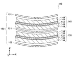
- FIG. 2 is a perspective view of the power storage element 110
- FIG. 3 is an enlarged cross-sectional view of the power storage element 110.
- the power storage element 110 has a negative electrode 130, a positive electrode 140, and a separator 150, and a laminated body in which these are laminated is wound around a winding core C. ..
- the winding core C does not necessarily have to be provided.
- the stacking order of the negative electrode 130, the positive electrode 140, and the separator 150 constituting the power storage element 110 is such that the separator 150, the negative electrode 130, the separator 150, and the positive electrode are stacked toward the winding core C side (from the outside of the winding).
- the order is 140.
- the power storage element 110 has a negative electrode terminal 131 and a positive electrode terminal 141 as shown in FIG.
- the negative electrode terminal 131 is connected to the negative electrode 130 and the positive electrode terminal 141 is connected to the positive electrode 140, and as shown in FIG. 2, they are respectively drawn out of the power storage element 110.
- the negative electrode 130 includes a negative electrode current collector 132, a negative electrode undercoat layer 133, and a negative electrode active material layer 134.
- the negative electrode current collector 132 is a metal foil, and the negative electrode undercoat layer 133 is formed on both the front and back surfaces of the negative electrode current collector 132.
- the negative electrode active material layer 134 is formed on the negative electrode undercoat layer 133.
- the positive electrode 140 includes a positive electrode current collector 142, a positive electrode undercoat layer 143, and a positive electrode active material layer 144.
- the positive electrode current collector 142 is a metal foil, and the positive electrode undercoat layer 143 is formed on both the front and back surfaces of the positive electrode current collector 142.
- the positive electrode active material layer 144 is formed on the positive electrode undercoat layer 143.
- One or both of the negative electrode 130 and the positive electrode 140 has a structure in which the active material layer is prevented from falling off as described later.
- the separator 150 insulates the negative electrode 130 and the positive electrode 140, and includes the first separator 151 and the second separator 152 as shown in FIG.
- the first separator 151 and the second separator 152 separate the negative electrode 130 and the positive electrode 140 and permeate the ions contained in the electrolytic solution described later.
- the first separator 151 and the second separator 152 may be a woven fabric, a non-woven fabric, a synthetic resin microporous film, or the like, and for example, a cellulosic resin may be used as a main material. it can.
- the first separator 151 and the second separator 152 may be one continuous separator.
- the container 120 houses the power storage element 110.
- the upper and lower surfaces of the container 120 can be closed by a lid (not shown).
- the material of the container 120 is not particularly limited, and may be made of, for example, aluminum, titanium, nickel, a metal containing iron as a main component, stainless steel, or the like.
- the power storage element 110 is housed in the container 120 together with the electrolytic solution.
- Electrolyte is not particularly limited, it may be a polycarbonate solution or the like of EDMI (ethyl dimethyl imidazolium) ⁇ BF 4.
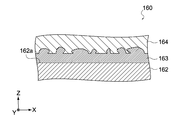
- FIG. 4 is a cross-sectional view of the electrode 160
- FIG. 5 is an enlarged view of a part of FIG.
- the electrode 160 includes a current collector 162, an undercoat layer 163, and an active material layer 164.
- the current collector 162 is a metal foil made of a metal such as aluminum.
- One main surface of the current collector 162 is referred to as a first main surface 162a, and the main surface on the opposite side thereof is referred to as a second main surface 162b.
- the thickness of the current collector can be, for example, 20 ⁇ m.
- the undercoat layer 163 is formed on the first main surface 162a and the second main surface 162b, and the active material layer 164 is brought into close contact with the current collector 162.
- the thickness of the undercoat layer 163 can be, for example, 3 ⁇ m.
- the undercoat layer 163 is made of a conductive material, and can be made of, for example, a material in which a polymer, inorganic particles, and a conductive auxiliary agent are mixed.
- polymer examples include polyvinyl alcohol, carboxymethyl cellulose, hydroxyethyl cellulose, polyacrylamide, epoxy resin, polyethyleneimine or polyacrylic acid ester. These may be used alone or in combination of two or more.
- inorganic particles examples include silica, titania, tin oxide, alumina, iron hydroxide, manganese hydroxide, magnesium hydroxide, silicon nitride, aluminum nitride, zirconia, barium titanate, and strontium carbonate. These may be used alone or in combination of two or more.
- the conductive auxiliary agent is a particle made of a conductive material, and examples thereof include metal powders such as Ag, Cu, and Al, carbon materials such as graphite and carbon black, and conductive polymers. These may be used alone or in combination of two or more.
- the undercoat layer 163 is provided with irregularities on the surface on the active material layer 164 side.
- the unevenness preferably has a central surface roughness (Ra) of 3.0 ⁇ m or more.
- the central surface roughness can be measured by taking a picture with a digital microscope (VHX-5000 manufactured by KEYENCE CORPORATION) and analyzing it.
- the active material layer 164 is formed on the undercoat layer 163.
- the thickness of the active material layer 164 can be, for example, 10 ⁇ m.
- the material of the active material layer 164 can be a mixture of the active material and the binder resin, and may further contain a conductive auxiliary material.
- carbon-based materials such as polyacene carbide, activated carbon, graphitized carbon (hard carbon), graphite and soft carbon, alloy-based materials such as Si and SiO, or composite materials thereof may be used. it can.
- the binder resin is a synthetic resin for bonding active materials, for example, styrene-butadiene rubber, polyethylene, polypropylene, aromatic polyamide, carboxymethyl cellulose, fluorine-based rubber, polyvinylidene fluoride, isoprene rubber, butadiene rubber, ethylene-propylene-based rubber, and the like. May be used.
- the conductive auxiliary agent is a particle made of a conductive material and improves the conductivity between the negative electrode active materials.
- Examples of the conductive auxiliary agent include carbon materials such as graphite and carbon black. These may be used alone or in combination of two or more.
- the conductive auxiliary agent may be a metal material, a conductive polymer, or the like as long as it is a conductive material.
- the electrode 160 has the above configuration. Although FIG. 5 shows the first main surface 162a side of the electrode 160, it can be assumed that the undercoat layer 163 is similarly formed with irregularities on the second main surface 162b side. Further, the undercoat layer 163 may have irregularities formed only on either the first main surface 162a side or the second main surface 162b side.
- the electrode 160 by providing the undercoat layer 163 with irregularities as described above, an anchor effect is generated between the undercoat layer 163 and the active material layer 164, and the physical connection is strengthened. As a result, the active material layer 164 is prevented from falling off.
- an undercoat layer 163 is formed on the surface of the current collector 162 by gravure printing. At this time, it is possible to form unevenness on the undercoat layer 163 by providing unevenness on the gravure printing mold.
- the active material layer 164 can be formed by discharging a slurry mixed with the materials from the die onto the undercoat layer 163.
- the electrode 160 can be used as either or both of the power storage element 110 negative electrode 130 and the positive electrode 140 (see FIG. 3).
- the undercoat layer 163 and the active material layer 164 may be formed on only one of the front and back surfaces of the current collector 161.
- the power storage element 110 is not limited to the winding type as shown in FIG. 2, and may be a laminated type in which the negative electrode 130 and the positive electrode 140 are laminated.
- Electrochemical device 110 ... Power storage element 120 ... Container 130 . Negative electrode 132 ; Negative electrode current collector 133 ... Negative electrode undercoat layer 134 ... Negative electrode active material layer 140 ... Positive electrode 142 ⁇ ⁇ ⁇ Positive electrode current collector 143 ⁇ ⁇ ⁇ Positive electrode undercoat layer 144 ⁇ ⁇ ⁇ Positive electrode active material layer 150 ⁇ ⁇ ⁇ Separator 160 ⁇ ⁇ ⁇ Electrode 162 ⁇ ⁇ ⁇ Electrode 162 ⁇ ⁇ ⁇ Current collector 163 ⁇ ⁇ ⁇ Undercoat layer 164 ⁇ ⁇ ⁇ Active material layer
Landscapes
- Engineering & Computer Science (AREA)
- Chemical & Material Sciences (AREA)
- Chemical Kinetics & Catalysis (AREA)
- Electrochemistry (AREA)
- General Chemical & Material Sciences (AREA)
- Power Engineering (AREA)
- Materials Engineering (AREA)
- Microelectronics & Electronic Packaging (AREA)
- Manufacturing & Machinery (AREA)
- General Physics & Mathematics (AREA)
- Inorganic Chemistry (AREA)
- Condensed Matter Physics & Semiconductors (AREA)
- Physics & Mathematics (AREA)
- Cell Electrode Carriers And Collectors (AREA)
- Secondary Cells (AREA)
- Electric Double-Layer Capacitors Or The Like (AREA)
Abstract
【課題】生産性に優れ、電極活物質層の脱落が生じにくい電極を備える電気化学デバイスを提供すること。 【解決手段】本発明に係る電気化学デバイスは、電極と、電解液とを具備する。上記電極は、金属箔である集電体と、上記集電体の主面上に形成され、凹凸を有する下塗り層と、上記下塗り層上に形成され、活物質を含む活物質層とを有する。上記電解液は、上記電極が浸漬される。
Description
本発明は、蓄電及び放電が可能な電気化学デバイスに関する。
PAS(Polyacenic Semiconductor)キャパシタ、電気二重層キャパシタ、リチウムイオン二次電池等の電気化学デバイスは正極と負極を、セパレータを介して交互に積層した蓄電素子を備える。
正極と負極は、金属箔である集電体の表面に電極活物質を積層した構造を有する。製造工程や充放電中にこの電極活物質が集電体から脱落すると、所望の電気特性を得られないため、集電体からの電極活物質の脱落が発生しないように検討が行われてきた。
例えば特許文献1には、集電体に貫通孔を設け、アンカー効果により集電体と電極活物質をつなぎとめる方法が開示されている。また、特許文献2には、平坦な集電体に下塗り層を形成し、その上に電極活物質層を積層することで、電極活物質の脱落を防止する方法が開示されている。
しかしながら、特許文献1に記載の方法では、集電体に貫通孔を形成することが困難であり、加工工数の増加が否めない。また、特許文献2に記載の方法では、均一な厚みの下塗り層を設けることが推奨されているが、下塗り層の表面が平滑であると下塗り層と電極活物質層の物理的なつながりが弱く、長期信頼性が問題となるおそれがある。
以上のような事情に鑑み、本発明の目的は、生産性に優れ、電極活物質層の脱落が生じにくい電極を備える電気化学デバイスを提供することにある。
上記目的を達成するため、本発明の一形態に係る電気化学デバイスは、電極と電解液とを具備する。
上記電極は、金属箔である集電体と、上記集電体の主面上に形成され、凹凸を有する下塗り層と、上記下塗り層上に形成され、活物質を含む活物質層とを有する。
上記電解液は、電極が浸漬される。
上記電極は、金属箔である集電体と、上記集電体の主面上に形成され、凹凸を有する下塗り層と、上記下塗り層上に形成され、活物質を含む活物質層とを有する。
上記電解液は、電極が浸漬される。
この構成によれば、凹凸を有する下塗り層と活物質層の間にアンカー効果が生じ、物理的なつながりが強化される。これにより、活物質層の脱落が防止されている。
上記下塗り層の中心表面粗さは3.0μm以上あってもよい。
上記電気化学デバイスは、ポリアセンキャパシタであってもよい。
上記目的を達成するため、本発明の一形態に係る電気化学デバイスは、正極と、負極と、セパレータと、電解液とを具備する。
上記正極は、金属箔である正極集電体と、上記正極集電体の主面上に形成され、凹凸を有する正極下塗り層と、上記正極下塗り層上に形成され、正極活物質を含む正極活物質層とを有する。
上記負極は、金属箔である負極集電体と、上記負極集電体の主面上に形成され、凹凸を有する負極下塗り層と、上記負極下塗り層上に形成され、負極活物質を含む負極活物質層とを有する。
上記セパレータは、上記正極と上記負極を絶縁する。
上記電解液は、上記正極、上記負極及び上記セパレータが浸漬される。
上記正極は、金属箔である正極集電体と、上記正極集電体の主面上に形成され、凹凸を有する正極下塗り層と、上記正極下塗り層上に形成され、正極活物質を含む正極活物質層とを有する。
上記負極は、金属箔である負極集電体と、上記負極集電体の主面上に形成され、凹凸を有する負極下塗り層と、上記負極下塗り層上に形成され、負極活物質を含む負極活物質層とを有する。
上記セパレータは、上記正極と上記負極を絶縁する。
上記電解液は、上記正極、上記負極及び上記セパレータが浸漬される。
以上のように本発明によれば、生産性に優れ、電極活物質層の脱落が生じにくい電極を備える電気化学デバイスを提供することが可能である。
本発明の実施形態に係る電気化学デバイスについて説明する。
本実施形態に係る電気化学デバイスは、PAS(Polyacenic Semiconductor)キャパシタ、電気二重層キャパシタ、リチウムイオン二次電池等の充放電が可能なデバイスであり、その種類は特に限定されない。なお、以下の図において、X、Y及びZ方向は相互に直交する3方向である。
[電気化学デバイスの構成]
図1は、本実施形態に係る電気化学デバイス100の構成を示す斜視図である。同図に示すように電気化学デバイス100は、蓄電素子110が容器120(蓋及び端子は図示略)に収容されている。容器120内には、蓄電素子110と共に電解液が収容されている。なお、本実施形態に係る電気化学デバイス100の構成は、図1をはじめ、以降の図に示す構成に限定されるものではない。
図1は、本実施形態に係る電気化学デバイス100の構成を示す斜視図である。同図に示すように電気化学デバイス100は、蓄電素子110が容器120(蓋及び端子は図示略)に収容されている。容器120内には、蓄電素子110と共に電解液が収容されている。なお、本実施形態に係る電気化学デバイス100の構成は、図1をはじめ、以降の図に示す構成に限定されるものではない。
図2は蓄電素子110の斜視図であり、図3は蓄電素子110の拡大断面図である。図2及び図3に示すように、蓄電素子110は、負極130、正極140及びセパレータ150を有し、これらが積層された積層体が捲回芯Cの回りに捲回されて構成されている。なお、捲回芯Cは必ずしも設けられなくてもよい。
蓄電素子110を構成する負極130、正極140、セパレータ150の積層順は、図2に示すように、捲回芯C側に向かって(捲回外側から)セパレータ150、負極130、セパレータ150、正極140の順となる。また、蓄電素子110は、図2に示すように負極端子131と正極端子141を有する。負極端子131は負極130、正極端子141は正極140に接続され、図2に示すように、それぞれ蓄電素子110の外部に引き出されている。
負極130は、図3に示すように、負極集電体132、負極下塗り層133及び負極活物質層134を備える。負極集電体132は金属箔であり、負極下塗り層133は負極集電体132の表裏両面に形成されている。負極活物質層134は、負極下塗り層133上に形成されている。
正極140は、図3に示すように、正極集電体142、正極下塗り層143及び正極活物質層144を備える。正極集電体142は金属箔であり、正極下塗り層143は正極集電体142の表裏両面に形成されている。正極活物質層144は、正極下塗り層143上に形成されている。
負極130と正極140のいずれか一方又は両方は、後述するように活物質層の脱落が防止された構造を有する。
セパレータ150は負極130と正極140を絶縁し、図3に示すように、第1セパレータ151及び第2セパレータ152を含む。
第1セパレータ151と第2セパレータ152は、負極130と正極140を隔て、後述する電解液中に含まれるイオンを透過する。具体的には、第1セパレータ151及び第2セパレータ152は、織布、不織布、合成樹脂微多孔膜等であるものとすることができ、例えばセルロース系樹脂を主材料としたものとすることができる。また、第1セパレータ151及び第2セパレータ152は連続した一枚のセパレータであってもよい。
容器120は、蓄電素子110を収容する。容器120の上面及び下面は図示しない蓋によって閉塞されるものとすることができる。容器120の材質は、特に限定されず、例えばアルミニウム、チタン、ニッケル、鉄を主成分とする金属又はステンレス等からなるものとすることができる。
蓄電素子110は、電解液と共に容器120に収容される。電解液は特に限定されないが、EDMI(エチルジメチルイミダゾリウム)・BF4のポリカーボネート溶液等とすることができる。
[電極の構造について]
上記負極130及び正極140として利用することが可能な電極160について説明する。図4は電極160の断面図であり、図5は図4の一部の拡大図である。
上記負極130及び正極140として利用することが可能な電極160について説明する。図4は電極160の断面図であり、図5は図4の一部の拡大図である。
図4に示すように、電極160は、集電体162、下塗り層163及び活物質層164を備える。
集電体162は、アルミニウム等の金属からなる金属箔である。集電体162の一方の主面を第1主面162aとし、その反対側の主面を第2主面162bとする。集電体の厚みは例えば20μmとすることができる。
下塗り層163は、第1主面162a及び第2主面162b上に形成され、活物質層164を集電体162に密着させる。下塗り層163の厚みは例えば3μmとすることができる。下塗り層163は、導電性を有する材料からなり、例えば高分子、無機粒子及び導電助剤を混合した材料からなるものとすることができる。
高分子は、ポリビニルアルコール、カルボキシメチルセルロース、ヒドロキシエチルセルロース、ポリアクリルアミド、エポキシ樹脂、ポリエチレンイミン又はポリアクリル酸エステルが挙げられる。これらは単独でもよいし、複数種が混合されてもよい。
無機粒子は、シリカ、チタニア、酸化スズ、アルミナ、水酸化鉄、水酸化マンガン、水酸化マグネシウム、窒化ケイ素、窒化アルミ、ジルコニア、チタン酸バリウム又は炭酸ストロンチウムが挙げられる。これらは単独でもよいし、複数種が混合されてもよい。
導電助剤は、導電性材料からなる粒子であり、例えば、Ag、Cu、Al等の金属粉末、黒鉛やカーボンブラック等の炭素材料、導電性高分子が挙げられる。これらは単独でもよいし、複数種が混合されてもよい。
下塗り層163は、図5に示すように、活物質層164側の表面に凹凸が設けられている。この凹凸は中心表面粗さ(Ra)が3.0μm以上が好適である。なお、中心表面粗さはデジタルマイクロスコープ(キーエンス社製 VHX-5000)で撮影し、解析することによって測定することができる。
活物質層164は、下塗り層163上に形成されている。活物質層164の厚みは例えば10μmとすることができる。活物質層164の材料は、活物質がバインダ樹脂と混合されたものとすることができ、さらに導電助材を含んでもよい。
活物質は、例えば、ポリアセン炭化物、活性炭、難黒鉛化炭素(ハードカーボン)、グラファイトやソフトカーボン等の炭素系材料や、Si、SiOなどの合金系材料、または、それらの複合材料を用いることができる。
バインダ樹脂は、活物質を接合する合成樹脂であり、例えばスチレンブタジエンゴム、ポリエチレン、ポリプロピレン、芳香族ポリアミド、カルボキシメチルセルロース、フッ素系ゴム、ポリビニリデンフルオライド、イソプレンゴム、ブタジエンゴム及びエチレンプロピレン系ゴム等を用いてもよい。
導電助剤は、導電性材料からなる粒子であり、負極活物質の間での導電性を向上させる。導電助剤は、例えば、黒鉛やカーボンブラック等の炭素材料が挙げられる。これらは単独でもよいし、複数種が混合されてもよい。なお、導電助剤は、導電性を有する材料であれば、金属材料あるいは導電性高分子などであってもよい。
電極160は以上のような構成を有する。なお、図5では、電極160の第1主面162a側を示すが、第2主面162b側も同様に下塗り層163に凹凸が形成されているものとすることができる。また、第1主面162a側と第2主面162b側のどちらか一方にのみ下塗り層163に凹凸が形成されていてもよい。
電極160では上記のように下塗り層163に凹凸を設けることにより、下塗り層163と活物質層164の間にアンカー効果が生じ、物理的なつながりが強化されている。これにより、活物質層164の脱落が防止されている。
また、集電体162に貫通孔等を形成する必要がないため、工数の増加が発生せず、生産性に優れている。
電極160の製造方法としては、集電体162の表面にグラビア印刷により下塗り層163を形成する。この際グラビア印刷の型に、凹凸を設けておくことにより、下塗り層163に凹凸を形成することが可能である。活物質層164は、材料を混合したスラリーをダイから下塗り層163上に吐出させることにより形成することが可能である。
電極160は、蓄電素子110負極130及び正極140(図3参照)のいずれか一方又は両方として用いることが可能である。なお、下塗り層163及び活物質層164は集電体161の表裏面のうち一方にのみ形成されてもよい。
また、蓄電素子110は図2に示すような捲回型のものに限られず、負極130と正極140が積層された積層型のものであってもよい。
100・・・電気化学デバイス
110・・・蓄電素子
120・・・容器
130・・・負極
132・・・負極集電体
133・・・負極下塗り層
134・・・負極活物質層
140・・・正極
142・・・正極集電体
143・・・正極下塗り層
144・・・正極活物質層
150・・・セパレータ
160・・・電極
162・・・集電体
163・・・下塗り層
164・・・活物質層
110・・・蓄電素子
120・・・容器
130・・・負極
132・・・負極集電体
133・・・負極下塗り層
134・・・負極活物質層
140・・・正極
142・・・正極集電体
143・・・正極下塗り層
144・・・正極活物質層
150・・・セパレータ
160・・・電極
162・・・集電体
163・・・下塗り層
164・・・活物質層
Claims (4)
- 金属箔である集電体と、前記集電体の主面上に形成され、凹凸を有する下塗り層と、前記下塗り層上に形成され、活物質を含む活物質層とを有する電極と、
前記電極が浸漬される電解液と
を具備する電気化学デバイス。 - 請求項1に記載の電気化学デバイスであって、
前記下塗り層の中心表面粗さは3.0μm以上である
電気化学デバイス。 - 請求項1又は2に記載の電気化学デバイスであって、
ポリアセンキャパシタである
電気化学デバイス。 - 金属箔である正極集電体と、前記正極集電体の主面上に形成され、凹凸を有する正極下塗り層と、前記正極下塗り層上に形成され、正極活物質を含む正極活物質層とを有する正極と、
金属箔である負極集電体と、前記負極集電体の主面上に形成され、凹凸を有する負極下塗り層と、前記負極下塗り層上に形成され、負極活物質を含む負極活物質層とを有する負極と、
前記正極と前記負極を絶縁するセパレータと、
前記正極、前記負極及び前記セパレータが浸漬される電解液と
を具備する電気化学デバイス。
Applications Claiming Priority (2)
| Application Number | Priority Date | Filing Date | Title |
|---|---|---|---|
| JP2019060208A JP2020161670A (ja) | 2019-03-27 | 2019-03-27 | 電気化学デバイス |
| JP2019-060208 | 2019-03-27 |
Publications (1)
| Publication Number | Publication Date |
|---|---|
| WO2020196241A1 true WO2020196241A1 (ja) | 2020-10-01 |
Family
ID=72609353
Family Applications (1)
| Application Number | Title | Priority Date | Filing Date |
|---|---|---|---|
| PCT/JP2020/012259 Ceased WO2020196241A1 (ja) | 2019-03-27 | 2020-03-19 | 電気化学デバイス |
Country Status (2)
| Country | Link |
|---|---|
| JP (1) | JP2020161670A (ja) |
| WO (1) | WO2020196241A1 (ja) |
Families Citing this family (1)
| Publication number | Priority date | Publication date | Assignee | Title |
|---|---|---|---|---|
| CN215451468U (zh) * | 2021-06-28 | 2022-01-07 | 比亚迪股份有限公司 | 电极极片、电化学装置和底涂装置 |
Citations (4)
| Publication number | Priority date | Publication date | Assignee | Title |
|---|---|---|---|---|
| JP2006210883A (ja) * | 2004-12-27 | 2006-08-10 | Matsushita Electric Ind Co Ltd | 分極性電極体とその製造方法、及びこれを用いた電気化学キャパシタ |
| JP2007067155A (ja) * | 2005-08-31 | 2007-03-15 | Mitsubishi Paper Mills Ltd | 電気化学素子用セパレータ |
| JP2013506299A (ja) * | 2009-09-24 | 2013-02-21 | コーニング インコーポレイテッド | 梨地コーティングを有する電流コレクタ |
| JP2015193233A (ja) * | 2014-03-28 | 2015-11-05 | 東洋アルミニウム株式会社 | 被覆アルミニウム材及びその製造方法 |
-
2019
- 2019-03-27 JP JP2019060208A patent/JP2020161670A/ja active Pending
-
2020
- 2020-03-19 WO PCT/JP2020/012259 patent/WO2020196241A1/ja not_active Ceased
Patent Citations (4)
| Publication number | Priority date | Publication date | Assignee | Title |
|---|---|---|---|---|
| JP2006210883A (ja) * | 2004-12-27 | 2006-08-10 | Matsushita Electric Ind Co Ltd | 分極性電極体とその製造方法、及びこれを用いた電気化学キャパシタ |
| JP2007067155A (ja) * | 2005-08-31 | 2007-03-15 | Mitsubishi Paper Mills Ltd | 電気化学素子用セパレータ |
| JP2013506299A (ja) * | 2009-09-24 | 2013-02-21 | コーニング インコーポレイテッド | 梨地コーティングを有する電流コレクタ |
| JP2015193233A (ja) * | 2014-03-28 | 2015-11-05 | 東洋アルミニウム株式会社 | 被覆アルミニウム材及びその製造方法 |
Also Published As
| Publication number | Publication date |
|---|---|
| JP2020161670A (ja) | 2020-10-01 |
Similar Documents
| Publication | Publication Date | Title |
|---|---|---|
| JP6608862B2 (ja) | ナノ多孔性セパレータ層を利用するリチウム電池 | |
| JP5073144B2 (ja) | リチウムイオン二次電池 | |
| WO2016161587A1 (en) | Electrode material and energy storage apparatus | |
| JPH09213338A (ja) | 電池及びリチウムイオン二次電池 | |
| JP2014013693A (ja) | リチウムイオン二次電池およびその製造方法 | |
| CN108666142B (zh) | 电化学器件 | |
| JP2002118036A (ja) | 蓄電用電子部品および複合電極体 | |
| US10410799B2 (en) | Electrochemical device | |
| JP4140517B2 (ja) | リチウムイオン二次電池およびその構成法 | |
| JP2017183539A (ja) | 電気化学デバイス | |
| KR102136599B1 (ko) | 전기 화학 디바이스 | |
| WO2020196241A1 (ja) | 電気化学デバイス | |
| WO2019167740A1 (ja) | 電気化学デバイスの製造方法品及び電気化学デバイス | |
| CN106328912B (zh) | 用于电池组电池的阳极、用制造阳极的方法和电池组电池 | |
| KR102546111B1 (ko) | 용량 및 출력 특성이 향상된 고출력 리튬 이온 커패시터 | |
| JP2021082754A (ja) | 電気化学デバイス | |
| JP2006196235A (ja) | 電池・キャパシタ複合素子 | |
| JP6895118B2 (ja) | 蓄電素子 | |
| JP2017073462A (ja) | 電気化学デバイス | |
| KR20200115175A (ko) | 전기 화학 디바이스 | |
| KR101357137B1 (ko) | 전극 조립체 및 이를 구비한 전기에너지 저장장치 | |
| KR20200125082A (ko) | 에너지 저장장치 | |
| KR20240006681A (ko) | 에너지 저장 소자, 에너지 저장 소자의 조립체 및 제조 방법 | |
| KR20260028238A (ko) | 전극 조립체 및 이를 구비한 이차 전지 | |
| CN114142173A (zh) | 一种具有一体化结构的芳纶涂覆锂电池隔膜 |
Legal Events
| Date | Code | Title | Description |
|---|---|---|---|
| 121 | Ep: the epo has been informed by wipo that ep was designated in this application |
Ref document number: 20778071 Country of ref document: EP Kind code of ref document: A1 |
|
| NENP | Non-entry into the national phase |
Ref country code: DE |
|
| 122 | Ep: pct application non-entry in european phase |
Ref document number: 20778071 Country of ref document: EP Kind code of ref document: A1 |