WO2020195366A1 - アンテナ装置 - Google Patents
アンテナ装置 Download PDFInfo
- Publication number
- WO2020195366A1 WO2020195366A1 PCT/JP2020/006486 JP2020006486W WO2020195366A1 WO 2020195366 A1 WO2020195366 A1 WO 2020195366A1 JP 2020006486 W JP2020006486 W JP 2020006486W WO 2020195366 A1 WO2020195366 A1 WO 2020195366A1
- Authority
- WO
- WIPO (PCT)
- Prior art keywords
- switch
- row
- antenna element
- bridge circuit
- turned
- Prior art date
- Legal status (The legal status is an assumption and is not a legal conclusion. Google has not performed a legal analysis and makes no representation as to the accuracy of the status listed.)
- Ceased
Links
Images





Classifications
-
- H—ELECTRICITY
- H01—ELECTRIC ELEMENTS
- H01Q—ANTENNAS, i.e. RADIO AERIALS
- H01Q1/00—Details of, or arrangements associated with, antennas
- H01Q1/50—Structural association of antennas with earthing switches, lead-in devices or lightning protectors
-
- H—ELECTRICITY
- H01—ELECTRIC ELEMENTS
- H01Q—ANTENNAS, i.e. RADIO AERIALS
- H01Q3/00—Arrangements for changing or varying the orientation or the shape of the directional pattern of the waves radiated from an antenna or antenna system
- H01Q3/24—Arrangements for changing or varying the orientation or the shape of the directional pattern of the waves radiated from an antenna or antenna system varying the orientation by switching energy from one active radiating element to another, e.g. for beam switching
-
- H—ELECTRICITY
- H01—ELECTRIC ELEMENTS
- H01Q—ANTENNAS, i.e. RADIO AERIALS
- H01Q1/00—Details of, or arrangements associated with, antennas
- H01Q1/27—Adaptation for use in or on movable bodies
- H01Q1/32—Adaptation for use in or on road or rail vehicles
- H01Q1/3208—Adaptation for use in or on road or rail vehicles characterised by the application wherein the antenna is used
- H01Q1/3233—Adaptation for use in or on road or rail vehicles characterised by the application wherein the antenna is used particular used as part of a sensor or in a security system, e.g. for automotive radar, navigation systems
- H01Q1/3241—Adaptation for use in or on road or rail vehicles characterised by the application wherein the antenna is used particular used as part of a sensor or in a security system, e.g. for automotive radar, navigation systems particular used in keyless entry systems
-
- H—ELECTRICITY
- H04—ELECTRIC COMMUNICATION TECHNIQUE
- H04B—TRANSMISSION
- H04B1/00—Details of transmission systems, not covered by a single one of groups H04B3/00 - H04B13/00; Details of transmission systems not characterised by the medium used for transmission
- H04B1/02—Transmitters
- H04B1/04—Circuits
-
- H—ELECTRICITY
- H04—ELECTRIC COMMUNICATION TECHNIQUE
- H04B—TRANSMISSION
- H04B1/00—Details of transmission systems, not covered by a single one of groups H04B3/00 - H04B13/00; Details of transmission systems not characterised by the medium used for transmission
- H04B1/06—Receivers
- H04B1/16—Circuits
- H04B1/18—Input circuits, e.g. for coupling to an antenna or a transmission line
-
- H—ELECTRICITY
- H04—ELECTRIC COMMUNICATION TECHNIQUE
- H04B—TRANSMISSION
- H04B1/00—Details of transmission systems, not covered by a single one of groups H04B3/00 - H04B13/00; Details of transmission systems not characterised by the medium used for transmission
- H04B1/38—Transceivers, i.e. devices in which transmitter and receiver form a structural unit and in which at least one part is used for functions of transmitting and receiving
- H04B1/3822—Transceivers, i.e. devices in which transmitter and receiver form a structural unit and in which at least one part is used for functions of transmitting and receiving specially adapted for use in vehicles
-
- H—ELECTRICITY
- H04—ELECTRIC COMMUNICATION TECHNIQUE
- H04B—TRANSMISSION
- H04B17/00—Monitoring; Testing
- H04B17/10—Monitoring; Testing of transmitters
- H04B17/15—Performance testing
- H04B17/18—Monitoring during normal operation
Definitions
- the antenna device particularly regarding the antenna device having a plurality of antenna elements.
- the H-bridge circuit may be used as the drive circuit to drive the antenna.
- Patent Document 1 discloses a technique for driving an LF antenna with an H-bridge circuit.
- the device described in Patent Document 1 includes one H-bridge circuit for one antenna element. Therefore, as the number of antenna elements increases, the number of H-bridge circuits increases.
- An object of the present disclosure is to provide an antenna device in which the number of H-bridge circuits is smaller than the number of antenna elements.
- the antenna device is An H-bridge circuit in which two sets of switch rows including two switch elements connected in series are configured, and the first switch row, which is one switch row, and the second switch row, which is another switch row, are parallel to each other.
- a single connection type antenna element which is an antenna element connected between two switch elements of the first switch row included in one H-bridge circuit and between two switch elements of the second switch row of the H-bridge circuit. It includes a composite connection type antenna element which is an antenna element connected between two switch elements included in the first switch row and between two switch elements included in the second switch row of another H-bridge circuit.
- the compound connection type antenna element is also connected to the H bridge circuit to which the single connection type antenna element is connected. Therefore, the number of H-bridge circuits can be reduced compared to the number of antenna elements.
- the stand-alone antenna element Since the stand-alone antenna element is connected to the first switch row and the second switch row of one H-bridge circuit, a current can be passed to the stand-alone antenna element in both directions using the one H-bridge circuit. For example, an alternating current flows through the stand-alone antenna element. By flowing an alternating current through the stand-alone antenna element, the stand-alone antenna element can function as an antenna.
- the composite connection type antenna element is a first switch array of one H-bridge circuit (referred to as a first H-bridge circuit) and a second switch of another H-bridge circuit (referred to as a second H-bridge circuit). Connected to a column.
- the composite connection type antenna element is connected to a third H-bridge circuit composed of a first switch row included in the first H-bridge circuit and a second switch row included in the second H-bridge circuit. It will be done. If a current is passed through the composite connection type antenna element in both directions using this third H-bridge circuit, the composite connection type antenna element can function as an antenna.
- FIG. 1 is a diagram showing a configuration of the antenna device 1 of the first embodiment.
- the antenna device 1 is mounted on the vehicle 2.
- the antenna device 1 includes an ECU (Electronic Control Unit) 10 and six antenna elements 30a, 30b, 30c, 30d, 30e, and 30f. When these six antenna elements 30a, 30b, 30c, 30d, 30e, and 30f are not distinguished, they are referred to as antenna element 30.
- the ECU 10 determines whether or not the legitimate electronic key 3 exists in the communication range of the antenna element 30 when a predetermined operation start condition is satisfied, such as when the vehicle 2 is stopped. For this determination, the ECU 10 causes the antenna element 30 to transmit a signal for detecting the existence of the regular electronic key 3.
- the electrical length of the antenna element 30 is the electrical length for transmitting and receiving radio waves in the LF band.
- the antenna element 30 does not have to be a single element, and may be configured to include a plurality of elements.
- the form of the portion of the antenna element 30 that emits radio waves can be various forms such as a coil type and a linear type.
- the antenna element 30 may include a capacitor, an impedance adjusting resistor, and the like in addition to the portion that emits radio waves.
- the position of the antenna element 30a is the door handle of the right door of the vehicle 2.
- the arrangement position of the antenna element 30b is the rear end surface of the vehicle 2.
- the position of the antenna element 30c is the door handle of the left door of the vehicle 2.
- the body of the vehicle 2 in the vicinity where these three antenna elements 30a, 30b, and 30c are arranged is made of metal. Therefore, the communication range of these three antenna elements 30a, 30b, and 30c is formed on the outside of the vehicle 2.
- a dashed line having a substantially radial shape centered on the antenna elements 30a, 30b, 30c conceptually indicates the communication range of the antenna elements 30a, 30b, 30c.
- the antenna element 30d is located at the front end of the passenger compartment.
- the position of the antenna element 30e is near the center of the passenger compartment.
- the antenna element 30f is near the rear end of the passenger compartment.
- the communication range of these antenna elements 30d, 30e, and 30f is in the vehicle interior.
- the antenna device 1 constitutes a part of an in-vehicle system that detects an electronic key 3 existing in the vehicle interior or in the vicinity of the vehicle 2.
- the in-vehicle system causes the electronic key 3 to transmit a request signal for a response from the antenna element 30 included in the antenna device 1 one by one in a predetermined order or from a plurality of antenna elements 30 at the same time.
- the electronic key 3 receives the request signal, it returns a response signal.
- the response signal is transmitted by radio waves in the RF band.
- the in-vehicle system includes an antenna for receiving a response signal.
- the number and position of the antenna elements 30 are not limited to the number and position shown in FIG.
- the number and position of the antenna elements 30 may be such that the electronic key 3 existing in the vehicle interior or in the vicinity of the vehicle 2 can be detected.
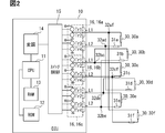
- FIG. 2 shows the configuration of the ECU 10.
- the ECU 10 includes a CPU 11, a ROM 12, a RAM 13, a modulation circuit 14, a switch control circuit 15, and three H-bridge circuits 16a, 16b, and 16c.
- the three H-bridge circuits 16a, 16b, and 16c are not distinguished, they are referred to as H-bridge circuits 16.
- the ROM 12 stores a program executed by the CPU 11.
- the CPU 11 realizes various functions by executing a program stored in the ROM while using the temporary storage function of the RAM 13.
- One of the functions realized by the CPU 11 is to output a base signal to the modulation circuit 14.
- the base signal is a signal carried by a carrier wave.
- the above-mentioned request signal is one of the base signals.
- the modulation circuit 14 generates a carrier signal that vibrates at the frequency of the carrier wave, and modulates the base signal with the generated carrier signal.
- the modulation method is, for example, the ASK method. Since there are high and low signal levels of the carrier signal, the signal modulated by the modulation circuit 14 becomes a signal in which the high signal and the low signal are repeated. This signal, in which the high signal and the low signal are repeated, is input to the switch control circuit 15.
- the switch control circuit 15 can separately turn on / off the transistors Tr included in the H-bridge circuit 16 one by one.
- the switch control circuit 15 can be realized by, for example, a microcontroller.
- the H-bridge circuit 16 includes four transistors Tr1, Tr2, Tr3, and Tr4 which are switch elements. These four transistors Tr1, Tr2, Tr3, and Tr4 are any MOSFETs. Further, in the H-bridge circuit 16 shown in FIG. 3, the transistors Tr1, Tr2, Tr3, and Tr4 are all N-type MOSFETs. However, P-type MOSFETs may be used for the high-side transistors Tr1 and Tr3.
- the H-bridge circuit 16a includes two sets of switch rows, a first switch row L1 and a second switch row L2.
- the first switch row L1 includes transistors Tr1 and Tr2 connected in series with each other
- the second switch row L2 includes transistors Tr3 and Tr4 connected in series with each other.
- the first switch row L1 and the second switch row L2 are in parallel with each other.
- Transistor Tr1 and transistor Tr3 are high-side transistors connected to the power supply.
- the transistors Tr2 and Tr4 are low-side transistors connected to the ground.
- One end of the antenna element 30a is connected between the source terminal of the transistor Tr1 and the drain terminal of the transistor Tr2.
- one end of the antenna element 30f is also connected between the source terminal of the transistor Tr1 and the drain terminal of the transistor Tr2, it is omitted in FIG.
- the other end of the antenna element 30a is connected between the source terminal of the transistor Tr3 and the drain terminal of the transistor Tr4 via the output adjustment resistor 31a.
- the output adjusting resistor 31a is a resistor for adjusting the output of the radio wave transmitted from the antenna element 30a for each antenna element 30.
- the switch control circuit 15 When a high signal is input and the H-bridge circuit 16a is a drive target, the switch control circuit 15 turns on the transistors Tr1 and Tr4 included in the H-bridge circuit 16a and turns off the transistors Tr2 and Tr3. As a result, a current flows through the antenna element 30a in the direction from top to bottom in FIG.
- the transistors Tr2 and Tr3 included in the H-bridge circuit 16a are turned on and the transistors Tr1 and Tr4 are turned off. At this time, a current flows through the antenna element 30a in the direction from the bottom to the top in FIG. Therefore, since alternating current flows through the antenna element 30a corresponding to the high signal and the low signal input to the switch control circuit 15, radio waves in the LF band are transmitted from the antenna element 30a.
- One end of the antenna element 30a is connected between the two transistors Tr1 and Tr2 of the first switch row L1 of the H-bridge circuit 16a, and the other end is between the two transistors Tr3 and Tr4 of the second switch row L2. It is connected to the.
- Both ends of this antenna element 30a are connected to the same H-bridge circuit 16a.
- the antenna element 30 whose both ends are connected to the same H-bridge circuit 16 is used as a single connection type antenna element.
- the antenna elements 30c and 30e are also independently connected antenna elements.
- One end of the antenna element 30c is connected between the transistors Tr1 and Tr2 of the H-bridge circuit 16b, and the other end is connected between the two transistors Tr3 and Tr4 of the H-bridge circuit 16b.
- One end of the antenna element 30e is connected between the transistors Tr1 and Tr2 of the H-bridge circuit 16c, and the other end is connected between the two transistors Tr3 and Tr4 of the H-bridge circuit 16c.
- the remaining three antenna elements 30b, 30d, and 30f differ in the H-bridge circuit 16 to which one end is connected and the H-bridge circuit 16 to which the other end is connected.
- Such an antenna element 30 is referred to as a composite connection type antenna element.
- One end of the antenna element 30b is connected between the two transistors Tr1 and Tr2 of the first switch row L1 of the H-bridge circuit 16b. Further, it can be said that one end of the antenna element 30b is branched from the line to which the antenna element 30c is connected to the H-bridge circuit 16b. This branching point is hereinafter referred to as a branching point 32bc.
- the other end of the antenna element 30b is connected between the two transistors Tr3 and Tr4 of the second switch row L2 of the H-bridge circuit 16c. It can be said that the other end of the antenna element 30b is branched from the line to which the antenna element 30e is connected to the H-bridge circuit 16c. This branching point is hereinafter referred to as a branching point 32be.
- One end of the antenna element 30d is connected between the two transistors Tr1 and Tr2 of the first switch row L1 of the H-bridge circuit 16c. Further, it can be said that one end of the antenna element 30d is branched from the line to which the antenna element 30e is connected to the H-bridge circuit 16c. This branching point is hereinafter referred to as a branching point 32de.
- the other end of the antenna element 30d is connected between the two transistors Tr3 and Tr4 of the second switch row L2 of the H-bridge circuit 16a. It can be said that the other end of the antenna element 30d is branched from the line to which the antenna element 30a is connected to the H-bridge circuit 16a. This branching point is hereinafter referred to as a branching point 32ad.
- One end of the antenna element 30f is connected between the two transistors Tr1 and Tr2 of the first switch row L1 of the H-bridge circuit 16a. Further, it can be said that one end of the antenna element 30f is branched from the line to which the antenna element 30a is connected to the H-bridge circuit 16a. This branching point is hereinafter referred to as a branching point 32af.
- the other end of the antenna element 30f is connected between the two transistors Tr3 and Tr4 of the second switch row L2 of the H-bridge circuit 16b. It can be said that the other end of the antenna element 30f is branched from the line to which the antenna element 30c is connected to the H-bridge circuit 16b.
- branching point 32cf This branching point is hereinafter referred to as a branching point 32cf.
- branch points 32bc, 32be, 32de, 32ad, 32af, and 32cf are described as branch points 32.
- Output adjustment resistors 31a, 31b, 31c, 31d, 31f are connected in series to all the antenna elements 30a, 30b, 30c, 30d, 30e, and 30f, respectively. When these output adjusting resistors 31a, 31b, 31c, 31d, and 31f are not distinguished, they are described as output adjusting resistors 31. Each of the output adjusting resistors 31 is arranged on the line on the antenna element 30 side of the branch point 32.
- the antenna device 1 has a smaller number of H-bridge circuits 16 for driving the antenna elements 30 than the number of antenna elements 30.
- the number of H-bridge circuits 16 is half the number of antenna elements 30.
- the antenna device 1 can individually transmit radio waves from all the antenna elements 30.
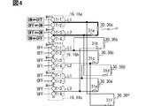
- FIG. 4 shows the independent control executed by the switch control circuit 15 when the radio wave is transmitted only from the antenna element 30a, which is an independently connected antenna element.
- the switch control circuit 15 turns on the transistors Tr1 and Tr4 and turns off the transistors Tr2 and Tr3 when a high signal is input to the H-bridge circuit 16a. Then, when the low signal is input, the transistors Tr2 and Tr3 are turned on, and the transistors Tr1 and Tr4 are turned off. As a result, alternating current that fluctuates at the frequency of the LF band flows through the antenna element 30a, so that radio waves in the LF band are transmitted from the antenna element 30a. Further, no radio wave is transmitted from the other antenna element 30.
- the thick line shown in FIG. 4 indicates the current path when an alternating current flows through the antenna element 30a.
- the thick line in FIG. 5 and below also shows the path through which the current flows by the on / off control described in each figure.
- the transistor Tr that is turned on when a high signal is input is referred to as a high-side transistor Tr
- the transistor Tr that is turned on when a low signal is input is referred to as a low-side transistor Tr.
- One state is a state in which the high-side transistor Tr of the H-bridge circuit 16b to which the antenna element 30c is connected is turned on and the low-side transistor Tr is turned off.
- the other state is a state in which the low-side transistor Tr is turned on and the high-side transistor Tr is turned off.
- One state is a state in which the high-side transistor Tr of the H-bridge circuit 16c to which the antenna element 30e is connected is turned on and the low-side transistor Tr is turned off.
- the other state is a state in which the low-side transistor Tr is turned on and the high-side transistor Tr is turned off.
- FIG. 5 shows composite control executed by the switch control circuit 15 when radio waves are transmitted only from the antenna element 30b, which is a composite connection type antenna element.
- the switch control circuit 15 switches the on / off state of the first switch row L1 of the H-bridge circuit 16b and the second switch row L2 of the H-bridge circuit 16c. Specifically, when a high signal is input, the transistor Tr1 of the H-bridge circuit 16b and the transistor Tr4 of the H-bridge circuit 16c are turned on, and the transistor Tr2 of the H-bridge circuit 16b and the transistor Tr3 of the H-bridge circuit 16c are turned off. To. On the other hand, when a low signal is input, the switch control circuit 15 turns on the transistor Tr2 of the H-bridge circuit 16b and the transistor Tr3 of the H-bridge circuit 16c.
- the transistor Tr1 of the H-bridge circuit 16b and the transistor Tr4 of the H-bridge circuit 16c are turned off.
- alternating current that fluctuates at the frequency of the LF band flows through the antenna element 30b, so that radio waves in the LF band are transmitted from the antenna element 30b. Further, no radio wave is transmitted from the other antenna element 30.
- the first switch row L1 of the H-bridge circuit 16c to which one end of the antenna element 30d is connected and the H-bridge circuit 16a to which the other end is connected are the first. 2 Switch train L2 is turned on and off. The on / off operation is the same as when transmitting radio waves from the antenna element 30b.
- the H-bridge circuit 16 to which both ends of the antenna element 30d are connected is a separate H-bridge circuit 16. However, both ends of the antenna element 30d are connected to the first switch row L1 and the second switch row L2. Therefore, the first switch row L1 and the second switch row L2 to which both ends of the antenna element 30d are connected can be regarded as one H-bridge circuit. By controlling the transistor Tr included in this H-bridge circuit on and off, radio waves can be transmitted from the antenna element 30d.
- the column L2 may be turned on and off.
- each of the antenna elements 30a, 30b, 30c, 30d, 30e, and 30f can be operated independently to transmit radio waves.
- the antenna device 1 can also transmit radio waves from a plurality of antenna elements 30 at the same time.
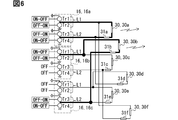
- FIG. 6 shows the on / off operation of the transistor Tr when radio waves are simultaneously transmitted from one single connection type antenna element and one composite connection type antenna element.
- the single connection type antenna element is the antenna element 30a
- the composite connection type antenna element is the antenna element 30b.
- the transistors Tr that operate these two antenna elements 30a and 30b do not overlap. Further, even if the transistor Tr is turned on to operate these two antenna elements 30a and 30b, no current flows through the other antenna elements 30. Therefore, when radio waves are transmitted from these two antenna elements 30a and 30b at the same time, the phase of the current flowing through the two antenna elements 30a and 30b does not matter.
- the switch control circuit 15 executes the first simultaneous control in order to transmit radio waves from the antenna element 30a. Along with this first simultaneous control, the switch control circuit 15 executes a second simultaneous control in order to transmit radio waves from the antenna element 30b.
- the first simultaneous control is almost the same as the independent control described with reference to FIG.
- the first simultaneous control executes the second simultaneous control at the same time. Therefore, in the first simultaneous control, the on / off control is not performed for the transistor Tr that is turned on / off in the second simultaneous control. Only this point is the difference between the first simultaneous control and the independent control.
- the second simultaneous control is almost the same as the combined control described with reference to FIG.
- the on / off control is not performed for the transistor Tr that is turned on / off in the first simultaneous control. Only this point is the difference between the second simultaneous control and the combined control.
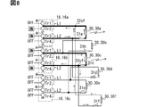
- 7 and 8 show the operation when radio waves are transmitted from two independently connected antenna elements at the same time.
- the switch control circuit 15 executes reverse phase simultaneous control.
- 7 and 8 are diagrams illustrating simultaneous reverse-phase control when radio waves are simultaneously transmitted from the antenna elements 30a and 30c, which are both independently connected antenna elements.
- the H-bridge circuit 16 including the transistor Tr that operates these two antenna elements 30a and 30c is the H-bridge circuits 16a and 16b.
- the H-bridge circuit 16a corresponds to the first H-bridge circuit
- the H-bridge circuit 16b corresponds to the second H-bridge circuit.
- the antenna element 30b is an antenna element 30 that operates the transistor Tr included in these two H-bridge circuits 16a and 16b to transmit radio waves. Therefore, when it is desired to transmit radio waves only from the two antenna elements 30a and 30c, it is necessary to reverse the phase of the current flowing through the antenna element 30a and the current flowing through the antenna element 30c. By repeating the state shown in FIG. 7 and the state shown in FIG. 8, the current flowing through the antenna element 30a and the current flowing through the antenna element 30c can be reversed in phase.
- the switch control circuit 15 is set to the state shown in FIG. 7 when a high signal is input.
- the high-side transistor Tr1 of the first switch row L1 of the H-bridge circuit 16a to which the antenna element 30a is connected and the low-side transistor Tr4 of the second switch row L2 of the H-bridge circuit 16a are turned on. I have to.
- the low-side transistor Tr2 of the first switch row L1 and the high-side transistor Tr3 of the second switch row L2 of the H-bridge circuit 16b are turned on. There is.
- the switch control circuit 15 is in the state shown in FIG. 8 when a low signal is input.
- the low-side transistor Tr2 of the first switch row L1 of the H-bridge circuit 16a to which the antenna element 30a is connected and the high-side transistor Tr3 of the second switch row L2 of the H-bridge circuit 16a are turned on. I have to.
- the high-side transistor Tr1 of the first switch row L1 and the low-side transistor Tr4 of the second switch row L2 of the H-bridge circuit 16b are turned on. There is.
- radio waves are transmitted only from these two antenna elements 30a and 30c by making the current flowing through the antenna element 30a and the current flowing through the antenna element 30c out of phase. Can be done.
- the antenna device 1 of the first form described above includes six antenna elements 30, but the H-bridge circuit 16 is three, which is half the number of the antenna elements 30. In this way, the number of H-bridge circuits 16 is smaller than the number of antenna elements 30.
- the independent control described with reference to FIG. 4 is performed for the H-bridge circuit 16 to which the antenna elements 30a, 30c, and 30e are connected, respectively. Just do it.
- FIG. 5 shows the first switch row L1 and the second switch row L2 to which the antenna elements 30b, 30d, 30f are connected.
- the compound control described with reference to may be executed. By executing these single control and combined control, even if the number of H-bridge circuits 16 is smaller than the number of antenna elements 30, all the antenna elements 30 can be driven individually.
- the antenna device 1 simultaneously executes the first simultaneous control and the second simultaneous control from one single connection type antenna element and one composite connection type antenna element. Radio waves can be transmitted at the same time. Further, as described with reference to FIGS. 7 and 8, the antenna device 1 can simultaneously transmit radio waves from two independently connected antenna elements by executing reverse phase simultaneous control. Therefore, the antenna device 1 can simultaneously transmit radio waves from any two antenna elements 30. By transmitting radio waves from the two antenna elements 30 at the same time, the electronic key 3 can be detected at an early stage, and various applied controls are possible.
- the antenna device 1 is provided with an output adjusting resistor 31 for adjusting the output of the antenna element 30 on the antenna element 30 side of the branch point 32.
- the output adjustment resistor 31 By arranging the output adjustment resistor 31 closer to the antenna element 30 than the branch point 32, the power of the radio wave transmitted from each antenna element 30 can be adjusted for each antenna element 30.
- FIG. 9 shows the configuration of the antenna device 100 of the second embodiment.
- the antenna device 100 is different from the antenna device 1 of the first embodiment in that it includes three disconnection detection circuits 40a, 40b, and 40c. When these three disconnection detection circuits 40a, 40b, and 40c are not distinguished, they are described as the disconnection detection circuit 40.
- the disconnection detection circuit 40 is provided separately from the ECU 10 for convenience of illustration, the disconnection detection circuit 40 may be provided inside the ECU 10.
- the disconnection detection circuit 40a detects the voltage at the connection point 33a.
- the connection point 33a is on the side farther from the two antenna elements 30a and 30d than the branch point 32ad.
- a current flows through the connection point 33a. Therefore, by detecting the voltage at the connection point 33a, the disconnection detection circuit 40a can detect the disconnection occurring in the line in which the two antenna elements 30a and 30d are connected to the H-bridge circuit 16.
- the disconnection detection circuit 40b detects the voltage at the connection point 33b.
- the connection point 33b is on the side farther from the two antenna elements 30c and 30f than the branch point 32cf.
- a current flows through the connection point 33b. Therefore, by detecting the voltage at the connection point 33b, the disconnection detection circuit 40b can detect the disconnection occurring in the line in which the two antenna elements 30c and 30f are connected to the H bridge circuit 16.
- the disconnection detection circuit 40c detects the voltage at the connection point 33c.
- the connection point 33c is on the side farther from the two antenna elements 30b and 30e than the branch point 32be. When the two antenna elements 30b and 30e operate, a current flows through the connection point 33c. Therefore, by detecting the voltage at the connection point 33c, the disconnection detection circuit 40c can detect the disconnection occurring in the line in which the two antenna elements 30b and 30e are connected to the H-bridge circuit 16.
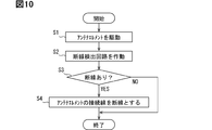
- FIG. 10 shows a disconnection detection process executed by the CPU 11 in order to detect a disconnection occurring in the line in which the antenna element 30a is connected to the H-bridge circuit 16.
- the disconnection detection process shown in FIG. 10 is executed every disconnection detection cycle during the activation of the ECU 10.
- the disconnection detection cycle can be set arbitrarily.
- an instruction to drive the antenna element 30a is output to the switch control circuit 15.
- the disconnection detection circuit 40a is operated.
- the detection result is acquired from the disconnection detection circuit 40a, and it is determined whether or not there is a disconnection based on the detection result. If it is determined that there is a disconnection, the process proceeds to S4.
- the connecting wire of the antenna element 30a is disconnected.
- a predetermined wire break detection process is executed, such as displaying a warning light provided on the instrument panel of the vehicle 2. If it is determined in the determination of S3 that there is no disconnection, the process shown in FIG. 10 is terminated without executing S4.
- the CPU 11 executes the same processing for the antenna elements 30c and 30e, and detects a disconnection of the line in which the antenna elements 30c and 30e are connected to the H bridge circuit 16.
- the process of detecting the disconnection of the line in which the antenna elements 30a, 30c, and 30e are connected to the H-bridge circuit 16 may be executed at different time zones or at the same time.
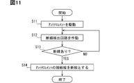
- the process shown in FIG. 11 is also a disconnection detection process executed by the CPU 11.
- the disconnection detection process shown in FIG. 11 is a process executed by the CPU 11 in order to detect a disconnection occurring in the line in which the antenna element 30b is connected to the H-bridge circuit 16.
- the disconnection detection process for detecting the disconnection occurring in the line in which the antenna elements 30d and 30f are connected to the H-bridge circuit 16 is the same as in FIG.
- the disconnection detection process shown in FIG. 11 is also executed every disconnection detection cycle during the activation of the ECU 10.
- the antenna element 30a is executing the disconnection detection process of the line connected to the H bridge circuit 16
- the disconnection detection process of the line connected to the H bridge circuit 16 by the antenna element 30d is not executed.
- the antenna element 30c is executing the disconnection detection process of the line connected to the H-bridge circuit 16
- the disconnection detection process of the line in which the antenna element 30f is connected to the H-bridge circuit 16 is not executed.
- the antenna element 30e is executing the disconnection detection process of the line connected to the H-bridge circuit 16
- the disconnection detection process of the line in which the antenna element 30b is connected to the H-bridge circuit 16 is not executed.
- an instruction to drive the antenna element 30b is output to the switch control circuit 15.
- the disconnection detection circuit 40c is operated.
- the detection result is acquired from the disconnection detection circuit 40c, and it is determined whether or not there is a disconnection based on the detection result. If it is determined that there is a disconnection, the process proceeds to S14.
- the connecting wire of the antenna element 30b is disconnected. If it is determined in the determination of S4 that there is no disconnection, the process shown in FIG. 11 is terminated without executing S14.
- the antenna device 100 of the second embodiment includes six antenna elements 30, but the disconnection detection circuit 40 is three, which is half the number of the antenna elements 30.
- the six antenna elements 30 are H-bridged, respectively. It is possible to detect a disconnection of the line connected to the circuit 16.
- the antenna element 30 included in the antenna devices 1 and 100 transmitted radio waves in the LF band.
- the frequency of the radio wave transmitted by the antenna element 30 may be other than the LF band.
- Modification 2 The number of antenna elements 30 of the antenna devices 1 and 100 was 6, and the number of H-bridge circuits 16 was half of that. However, as long as the number of antenna elements 30 is plural, the number may be other than 6. Further, the number of H-bridge circuits 16 may be smaller than that of the antenna elements 30, and may not be half of the number of antenna elements 30.
- the output adjusting resistor 31 is provided for all the antenna elements 30. However, the output adjusting resistor 31 may be provided only for a part of the antenna elements 30.
- Modification example 4 In the embodiment, the CPU 11 executes the disconnection detection process. However, the switch control circuit 15 may execute the disconnection detection process.
- the ECU 10 and the method executed by the ECU 10 described in the present disclosure may be realized by a dedicated computer constituting a processor programmed to execute one or a plurality of functions embodied by a computer program.
- the ECU 10 and the method executed by the ECU 10 described in the present disclosure may be realized by a dedicated hardware logic circuit.
- the ECU 10 and the method executed by the ECU 10 described in the present disclosure may be realized by one or more dedicated computers configured by a combination of a processor that executes a computer program and one or more hardware logic circuits. Good.
- the hardware logic circuit is, for example, ASIC or FPGA.
- the storage medium for storing the computer program is not limited to ROM 12, and may be stored in a computer-readable non-transition tangible recording medium as an instruction executed by the computer.
- the above program may be stored in the flash memory.
- each step is expressed as, for example, S1. Further, each step can be divided into a plurality of substeps, while the plurality of steps can be combined into one step.
Landscapes
- Engineering & Computer Science (AREA)
- Computer Networks & Wireless Communication (AREA)
- Signal Processing (AREA)
- Computer Security & Cryptography (AREA)
- Radar, Positioning & Navigation (AREA)
- Remote Sensing (AREA)
- Physics & Mathematics (AREA)
- Electromagnetism (AREA)
- Variable-Direction Aerials And Aerial Arrays (AREA)
- Details Of Aerials (AREA)
- Transmitters (AREA)
Abstract
アンテナ装置は、第1スイッチ列(L1)と他の前記スイッチ列である第2スイッチ列(L2)が互いに並列になっている、複数のHブリッジ回路(16)と、1つの前記Hブリッジ回路が備える前記第1スイッチ列の2つの前記スイッチ素子間と、当該Hブリッジ回路の前記第2スイッチ列の2つの前記スイッチ素子間とに接続されたアンテナエレメントである単独接続型アンテナエレメントと、前記第1スイッチ列が備える2つの前記スイッチ素子間と、他の前記Hブリッジ回路の前記第2スイッチ列が備える2つの前記スイッチ素子間とに接続されたアンテナエレメントである複合接続型アンテナエレメントと、を備える。
Description
本出願は、2019年3月27日に出願された日本国特許出願2019-61698号に基づくものであり、ここにその記載内容を参照により援用する。
アンテナ装置に関し、特に、複数のアンテナエレメントを備えるアンテナ装置に関する。
アンテナを駆動する駆動回路としてHブリッジ回路を用いることがある。特許文献1には、Hブリッジ回路でLFアンテナを駆動させる技術が開示されている。
特許文献1に記載された装置は、1つのアンテナエレメントに対して1つのHブリッジ回路を備えている。したがって、アンテナエレメントの数が増えるとHブリッジ回路が多くなってしまう。
本開示は、アンテナエレメントの数よりもHブリッジ回路の数が少ないアンテナ装置を提供することを目的とする。
本開示の一態様によれば、アンテナ装置は、
直列に接続された2つのスイッチ素子を備えるスイッチ列が2組構成され、1つのスイッチ列である第1スイッチ列と他のスイッチ列である第2スイッチ列が互いに並列になっているHブリッジ回路を複数備え、
1つのHブリッジ回路が備える第1スイッチ列の2つのスイッチ素子間と、そのHブリッジ回路の第2スイッチ列の2つのスイッチ素子間とに接続されたアンテナエレメントである単独接続型アンテナエレメントと、
第1スイッチ列が備える2つのスイッチ素子間と、他のHブリッジ回路の第2スイッチ列が備える2つのスイッチ素子間とに接続されたアンテナエレメントである複合接続型アンテナエレメントと、を備える。
直列に接続された2つのスイッチ素子を備えるスイッチ列が2組構成され、1つのスイッチ列である第1スイッチ列と他のスイッチ列である第2スイッチ列が互いに並列になっているHブリッジ回路を複数備え、
1つのHブリッジ回路が備える第1スイッチ列の2つのスイッチ素子間と、そのHブリッジ回路の第2スイッチ列の2つのスイッチ素子間とに接続されたアンテナエレメントである単独接続型アンテナエレメントと、
第1スイッチ列が備える2つのスイッチ素子間と、他のHブリッジ回路の第2スイッチ列が備える2つのスイッチ素子間とに接続されたアンテナエレメントである複合接続型アンテナエレメントと、を備える。
このアンテナ装置は、単独接続型アンテナエレメントが接続されているHブリッジ回路に、複合接続型アンテナエレメントも接続されている。したがって、アンテナエレメントの数よりもHブリッジ回路の数を少なくすることができる。
単独接続型アンテナエレメントは、1つのHブリッジ回路の第1スイッチ列と第2スイッチ列に接続されているので、その1つのHブリッジ回路を用いて単独接続型アンテナエレメントに双方向に電流を流せば、単独接続型アンテナエレメントに交流電流が流れる。単独接続型アンテナエレメントに交流電流が流れることで、単独接続型アンテナエレメントをアンテナとして機能させることができる。
一方、複合接続型アンテナエレメントは、1つのHブリッジ回路(第1のHブリッジ回路とする)の第1スイッチ列と、他のHブリッジ回路(第2のHブリッジ回路とする)の第2スイッチ列に接続されている。この接続構成により、複合接続型アンテナエレメントは、第1のHブリッジ回路が備える第1スイッチ列と第2のHブリッジ回路が備える第2スイッチ列とにより構成される第3のHブリッジ回路に接続されていることになる。この第3のHブリッジ回路を用いて複合接続型アンテナエレメントに双方向に電流を流せば、複合接続型アンテナエレメントをアンテナとして機能させることができる。
本開示についての目的、特徴や利点は、添付図面を参照した下記詳細な説明から、より明確になる。添付図面において、
アンテナ装置の構成を示す図である。
ECUの構成を示す図である。
Hブリッジ回路の構成を説明する図である。
アンテナエレメントのみから電波を送信する場合のオンオフ制御を示す図である。
アンテナエレメントのみから電波を送信する場合のオンオフ制御を示す図である。
アンテナエレメントから電波を送信する場合のオンオフ制御を示す図である。
アンテナエレメントから電波を送信する場合のオンオフ制御を示す図である。
アンテナエレメントから電波を送信する場合のオンオフ制御を示す図である。
アンテナ装置の構成を示す図である。
CPUが実行する断線検出処理を示すフローチャートである。
CPUが実行する断線検出処理を示すフローチャートである。
(第1実施形態)
以下、実施形態を図面に基づいて説明する。図1は、第1実施形態のアンテナ装置1の構成を示す図である。アンテナ装置1は、車両2に搭載されている。アンテナ装置1は、ECU(Electronic Control Unit)10と、6つのアンテナエレメント30a、30b、30c、30d、30e、30fを備える。これら6つのアンテナエレメント30a、30b、30c、30d、30e、30fを区別しないときはアンテナエレメント30と記載する。
以下、実施形態を図面に基づいて説明する。図1は、第1実施形態のアンテナ装置1の構成を示す図である。アンテナ装置1は、車両2に搭載されている。アンテナ装置1は、ECU(Electronic Control Unit)10と、6つのアンテナエレメント30a、30b、30c、30d、30e、30fを備える。これら6つのアンテナエレメント30a、30b、30c、30d、30e、30fを区別しないときはアンテナエレメント30と記載する。
ECU10は、車両2が停車状態であるなど、所定の動作開始条件が成立している場合に、アンテナエレメント30の通信範囲に正規の電子キー3が存在しているかどうかを判断する。この判断のために、ECU10は、アンテナエレメント30から、正規の電子キー3が存在していることを検出するための信号を送信させる。
アンテナエレメント30の電気長は、本実施形態では、LF帯の電波を送受信する電気長である。アンテナエレメント30は、単一の素子である必要はなく、複数のエレメントを備えた構成でもよい。アンテナエレメント30において電波を放射する部分の形態は、コイル型、線状型など種々の形態とすることができる。また、アンテナエレメント30は、電波を放射する部分の他に、コンデンサ、インピーダンス調整抵抗などを備えることもできる。
アンテナエレメント30aの配置位置は、車両2の右ドアのドアハンドルである。アンテナエレメント30bの配置位置は、車両2の後端面である。アンテナエレメント30cの配置位置は、車両2の左ドアのドアハンドルである。これら3つのアンテナエレメント30a、30b、30cが配置されている付近の車両2のボディは金属製である。したがって、これら3つのアンテナエレメント30a、30b、30cの通信範囲は、車両2の外側に形成される。図1において、アンテナエレメント30a、30b、30cを中心とする略半径形状の破線が、それらアンテナエレメント30a、30b、30cの通信範囲を概念的に示している。
アンテナエレメント30dの配置位置は車室前端である。アンテナエレメント30eの配置位置は車室中央付近である。アンテナエレメント30fは車室後端付近である。これらのアンテナエレメント30d、30e、30fの通信範囲は車室内である。
アンテナ装置1は、車室内または車両2の周辺に存在する電子キー3を検出する車載システムの一部を構成している。車載システムは、アンテナ装置1が備えるアンテナエレメント30から、所定の順番で1つずつ、あるいは複数のアンテナエレメント30から同時に、電子キー3に応答を求めるリクエスト信号を送信させる。電子キー3はリクエスト信号を受信すると、レスポンス信号を返信する。レスポンス信号はRF帯の電波で送信される。車載システムはレスポンス信号を受信するためのアンテナを備える。
なお、アンテナエレメント30の数および位置は、図1に示した数および位置に限られない。アンテナエレメント30の数および位置は、車室内または車両2の周辺に存在する電子キー3を検出できるようになっていればよい。
図2にECU10の構成を示す。図2に示すように、ECU10は、CPU11、ROM12、RAM13、変調回路14、スイッチ制御回路15、および3つのHブリッジ回路16a、16b、16cを備えている。3つのHブリッジ回路16a、16b、16cを区別しないときは、Hブリッジ回路16と記載する。
ROM12には、CPU11が実行するプログラムが格納されている。CPU11は、RAM13の一時記憶機能を利用しつつ、ROMに記憶されたプログラムを実行することで、種々の機能を実現する。CPU11が実現する機能の1つは、変調回路14へベース信号を出力することである。ベース信号は、搬送波により搬送される信号である。前述したリクエスト信号は、ベース信号の1つである。
変調回路14は、搬送波の周波数で振動する搬送波信号を生成し、生成した搬送波信号によりベース信号を変調する。変調方式は、たとえばASK方式である。搬送波信号の信号レベルにハイとローがあるため、変調回路14により変調された信号は、ハイ信号とロー信号が繰り返される信号になる。ハイ信号とロー信号が繰り返されるこの信号が、スイッチ制御回路15に入力される。スイッチ制御回路15は、Hブリッジ回路16が備えるトランジスタTrを、1つずつ別々にオンオフ制御することができる。スイッチ制御回路15は、たとえばマイクロコントローラにより実現できる。
Hブリッジ回路16の構成を図3を用いて説明する。図3には、Hブリッジ回路16aを示しているが、他のブリッジ回路16b、16cも同じ構成である。図3に示すように、Hブリッジ回路16aは、スイッチ素子である4つのトランジスタTr1、Tr2、Tr3、Tr4を備えている。これら4つのトランジスタTr1、Tr2、Tr3、Tr4は、いずれのMOSFETである。また、図3に示すHブリッジ回路16では、トランジスタTr1、Tr2、Tr3、Tr4は、いずれもN型MOSFETである。ただし、ハイサイドのトランジスタTr1、Tr3にP型MOSFETを用いてもよい。
Hブリッジ回路16aは、第1スイッチ列L1、第2スイッチ列L2の2組のスイッチ列を備えている。第1スイッチ列L1は、互いに直列接続されているトランジスタTr1、Tr2を備えており、第2スイッチ列L2は互いに直列接続されているトランジスタTr3、Tr4を備えている。これら第1スイッチ列L1と第2スイッチ列L2は互いに並列である。
トランジスタTr1、トランジスタTr3は、電源に接続されているハイサイドのトランジスタである。一方、トランジスタTr2、Tr4はグランドに接続されているローサイドのトランジスタである。
アンテナエレメント30aの一方の端は、トランジスタTr1のソース端子とトランジスタTr2のドレイン端子の間に接続されている。なお、アンテナエレメント30fの一方の端もトランジスタTr1のソース端子とトランジスタTr2のドレイン端子の間に接続されているが、図3では省略している。
アンテナエレメント30aの他方の端は、出力調整抵抗31aを介して、トランジスタTr3のソース端子とトランジスタTr4のドレイン端子の間に接続されている。出力調整抵抗31aは、アンテナエレメント30aから送信される電波の出力を、アンテナエレメント30別に調整するための抵抗である。
スイッチ制御回路15は、ハイ信号が入力され、かつ、Hブリッジ回路16aが駆動対象となっている場合、Hブリッジ回路16aが備えるトランジスタTr1、Tr4をオンにし、トランジスタTr2、Tr3をオフにする。これにより、アンテナエレメント30aには、図3において上から下に向かう方向に電流が流れる。一方、ロー信号が入力され、かつ、Hブリッジ回路16aが駆動対象になっている場合、Hブリッジ回路16aが備えるトランジスタTr2、Tr3をオンにし、トランジスタTr1、Tr4をオフにする。このときは、アンテナエレメント30aには、図3において下から上に向かう方向に電流が流れる。したがって、スイッチ制御回路15に入力されるハイ信号とロー信号に対応して、アンテナエレメント30aに交流が流れるので、アンテナエレメント30aからLF帯の電波が送信される。
説明を図2に戻す。アンテナエレメント30aは、一方の端がHブリッジ回路16aの第1スイッチ列L1の2つのトランジスタTr1、Tr2の間に接続され、他方の端が第2スイッチ列L2の2つのトランジスタTr3、Tr4の間に接続されている。
このアンテナエレメント30aは、両端が、同じHブリッジ回路16aに接続されている。両端が同じHブリッジ回路16に接続されているアンテナエレメント30を単独接続型アンテナエレメントとする。残りの5つのアンテナエレメント30のうち、アンテナエレメント30c、30eも単独接続型アンテナエレメントである。アンテナエレメント30cは、一方の端がHブリッジ回路16bのトランジスタTr1、Tr2の間に接続され、他方の端がHブリッジ回路16bの2つのトランジスタTr3、Tr4の間に接続されている。アンテナエレメント30eは、一方の端がHブリッジ回路16cのトランジスタTr1、Tr2の間に接続され、他方の端がHブリッジ回路16cの2つのトランジスタTr3、Tr4の間に接続されている。
残りの3つのアンテナエレメント30b、30d、30fは、一方の端が接続されているHブリッジ回路16と他方の端が接続されているHブリッジ回路16が相違する。このようなアンテナエレメント30を複合接続型アンテナエレメントとする。
アンテナエレメント30bは、一方の端がHブリッジ回路16bの第1スイッチ列L1の2つのトランジスタTr1、Tr2の間に接続されている。また、アンテナエレメント30bの一方の端は、Hブリッジ回路16bにアンテナエレメント30cが接続されている線路から分岐しているとも言える。この分岐している点を、以下、分岐点32bcとする。アンテナエレメント30bの他方の端は、Hブリッジ回路16cの第2スイッチ列L2の2つのトランジスタTr3、Tr4の間に接続されている。アンテナエレメント30bの他方の端は、Hブリッジ回路16cにアンテナエレメント30eが接続されている線路から分岐しているとも言える。この分岐している点を、以下、分岐点32beとする。
アンテナエレメント30dは、一方の端がHブリッジ回路16cの第1スイッチ列L1の2つのトランジスタTr1、Tr2の間に接続されている。また、アンテナエレメント30dの一方の端は、Hブリッジ回路16cにアンテナエレメント30eが接続されている線路から分岐しているとも言える。この分岐している点を、以下、分岐点32deとする。アンテナエレメント30dの他方の端はHブリッジ回路16aの第2スイッチ列L2の2つのトランジスタTr3、Tr4の間に接続されている。アンテナエレメント30dの他方の端は、Hブリッジ回路16aにアンテナエレメント30aが接続されている線路から分岐しているとも言える。この分岐している点を、以下、分岐点32adとする。
アンテナエレメント30fは、一方の端がHブリッジ回路16aの第1スイッチ列L1の2つのトランジスタTr1、Tr2の間に接続されている。また、アンテナエレメント30fの一方の端は、Hブリッジ回路16aにアンテナエレメント30aが接続されている線路から分岐しているとも言える。この分岐している点を、以下、分岐点32afとする。アンテナエレメント30fの他方の端はHブリッジ回路16bの第2スイッチ列L2の2つのトランジスタTr3、Tr4の間に接続されている。アンテナエレメント30fの他方の端は、Hブリッジ回路16bにアンテナエレメント30cが接続されている線路から分岐しているとも言える。この分岐している点を、以下、分岐点32cfとする。以下、6つの分岐点32bc、32be、32de、32ad、32af、32cfを区別しないときは分岐点32と記載する。
全部のアンテナエレメント30a、30b、30c、30d、30e、30fには、それぞれ、出力調整抵抗31a、31b、31c、31d、31fが直列接続されている。これら出力調整抵抗31a、31b、31c、31d、31fを区別しないときは、出力調整抵抗31と記載する。いずれの出力調整抵抗31も、分岐点32よりもアンテナエレメント30側の線路に配置されている。
この図2に示すように、アンテナ装置1は、アンテナエレメント30の数よりも、アンテナエレメント30を駆動するHブリッジ回路16の数が少ない。具体的には、Hブリッジ回路16の数はアンテナエレメント30の数の半分である。しかし、このようにアンテナエレメント30の数よりもHブリッジ回路16の数が少なくても、アンテナ装置1は、全部のアンテナエレメント30から、個別に電波を送信することができる。
(単独送信作動)
全部のアンテナエレメント30から個別に電波を送信するために、スイッチ制御回路15が実行するトランジスタTrのオンオフ制御を説明する。
全部のアンテナエレメント30から個別に電波を送信するために、スイッチ制御回路15が実行するトランジスタTrのオンオフ制御を説明する。
1つの単独接続型アンテナエレメントのみから電波を送信する場合にスイッチ制御回路15が実行するトランジスタTrのオンオフ制御を説明する。このときの制御を単独制御とする。図4には、単独接続型アンテナエレメントであるアンテナエレメント30aのみから電波を送信する場合にスイッチ制御回路15が実行する単独制御を示している。
図4に示すように、アンテナエレメント30aのみから電波を送信する場合、Hブリッジ回路16b、16cが備えるトランジスタTrは全部オフ状態を継続する。一方、スイッチ制御回路15は、Hブリッジ回路16aについては、ハイ信号が入力されたときは、トランジスタTr1、Tr4をオンさせ、トランジスタTr2、Tr3はオフする。そして、ロー信号が入力されたときは、トランジスタTr2、Tr3をオンさせ、トランジスタTr1、Tr4はオフする。これにより、アンテナエレメント30aには、LF帯の周波数で変動する交流が流れるので、アンテナエレメント30aからLF帯の電波が送信される。また、その他のアンテナエレメント30からは電波が送信されない。なお、図4に示す太線は、アンテナエレメント30aに交流電流が流れる場合の電流経路を示している。図5以下の太線も、各図に記載されているオンオフ制御により電流が流れる経路を示している。
以下の説明では、ハイ信号が入力されたときにオンさせるトランジスタTrをハイ側のトランジスタTrとし、ロー信号が入力されたときにオンさせるトランジスタTrをロー側のトランジスタTrとする。
アンテナエレメント30cから電波を送信する場合には、次の2つの状態を交互に繰り返す。1つの状態は、そのアンテナエレメント30cが接続されているHブリッジ回路16bのハイ側のトランジスタTrをオンにしロー側のトランジスタTrをオフにする状態である。もう1つの状態は、ロー側のトランジスタTrをオンにしハイ側のトランジスタTrをオフにする状態である。
アンテナエレメント30eから電波を送信する場合には、次の2つの状態を交互に繰り返す。1つの状態は、そのアンテナエレメント30eが接続されているHブリッジ回路16cのハイ側のトランジスタTrをオンにしロー側のトランジスタTrをオフにする状態である。もう1つの状態は、ロー側のトランジスタTrをオンにしハイ側のトランジスタTrをオフにする状態である。
1つの複合接続型アンテナエレメントのみから電波を送信する場合にスイッチ制御回路15が実行するトランジスタTrのオンオフ制御を説明する。このときの制御を複合制御とする。図5には、複合接続型アンテナエレメントであるアンテナエレメント30bのみから電波を送信する場合にスイッチ制御回路15が実行する複合制御を示している。
図5に示すように、アンテナエレメント30bのみから電波を送信する場合、Hブリッジ回路16aが備えるトランジスタTrは全部オフ状態を継続する。また、Hブリッジ回路16bの第2スイッチ列L2が備える2つのトランジスタTr、および、Hブリッジ回路16cの第1スイッチ列L1が備える2つのトランジスタTrもオフ状態を継続する。
一方、スイッチ制御回路15は、Hブリッジ回路16bの第1スイッチ列L1およびHブリッジ回路16cの第2スイッチ列L2についてはオンオフ状態を切り替える。具体的には、ハイ信号が入力されたときは、Hブリッジ回路16bのトランジスタTr1とHブリッジ回路16cのトランジスタTr4をオンにし、Hブリッジ回路16bのトランジスタTr2とHブリッジ回路16cのトランジスタTr3をオフにする。一方、ロー信号が入力されたときは、スイッチ制御回路15は、Hブリッジ回路16bのトランジスタTr2とHブリッジ回路16cのトランジスタTr3をオンにする。また、それとともに、Hブリッジ回路16bのトランジスタTr1とHブリッジ回路16cのトランジスタTr4をオフにする。これにより、アンテナエレメント30bには、LF帯の周波数で変動する交流が流れるので、アンテナエレメント30bからLF帯の電波が送信される。また、その他のアンテナエレメント30からは電波が送信されない。
アンテナエレメント30dから電波を送信する場合には、そのアンテナエレメント30dの一方の端が接続されているHブリッジ回路16cの第1スイッチ列L1および他方の端が接続されているHブリッジ回路16aの第2スイッチ列L2をオンオフ動作する。オンオフ動作のさせ方は、アンテナエレメント30bから電波を送信する場合と同じである。アンテナエレメント30dの両端がそれぞれ接続されているHブリッジ回路16は別々のHブリッジ回路16である。しかし、アンテナエレメント30dの両端は、第1スイッチ列L1および第2スイッチ列L2に接続されている。したがって、アンテナエレメント30dの両端がそれぞれ接続されている第1スイッチ列L1、第2スイッチ列L2を1つのHブリッジ回路と見ることができる。このHブリッジ回路が備えるトランジスタTrをオンオフ制御することで、アンテナエレメント30dから電波を送信することができる。
アンテナエレメント30fから電波を送信する場合、そのアンテナエレメント30fの一方の端が接続されているHブリッジ回路16aの第1スイッチ列L1と他方の端が接続されているHブリッジ回路16bの第2スイッチ列L2をオンオフ動作すればよい。
以上の説明で、各アンテナエレメント30a、30b、30c、30d、30e、30fのそれぞれを単独で動作させて電波を送信できることを説明した。
(同時送信作動)
アンテナ装置1は、複数のアンテナエレメント30から同時に電波を送信させることもできる。図6には、1つの単独接続型アンテナエレメントと、1つの複合接続型アンテナエレメントから同時に電波を送信させる場合のトランジスタTrのオンオフ作動を示している。
アンテナ装置1は、複数のアンテナエレメント30から同時に電波を送信させることもできる。図6には、1つの単独接続型アンテナエレメントと、1つの複合接続型アンテナエレメントから同時に電波を送信させる場合のトランジスタTrのオンオフ作動を示している。
図6に示す例は、単独接続型アンテナエレメントがアンテナエレメント30aであり、複合接続型アンテナエレメントがアンテナエレメント30bである。これら2つのアンテナエレメント30a、30bを動作させるトランジスタTrは重複していない。また、これら2つのアンテナエレメント30a、30bを動作させるためにトランジスタTrをオンさせても他のアンテナエレメント30に電流は流れない。したがって、これら2つのアンテナエレメント30a、30bから同時に電波を送信させる場合、2つのアンテナエレメント30a、30bに流れる電流の位相は問題にならない。
アンテナエレメント30aとアンテナエレメント30bから同時に電波を送信させる場合、スイッチ制御回路15は、アンテナエレメント30aから電波を送信させるために、第1同時制御を実行する。この第1同時制御とともに、スイッチ制御回路15は、アンテナエレメント30bから電波を送信させるために、第2同時制御を実行する。
第1同時制御は、図4を用いて説明した単独制御とほぼ同じである。第1同時制御は、同時に、第2同時制御を実行する。したがって、第1同時制御では第2同時制御でオンオフするトランジスタTrについてはオンオフ制御しない。この点のみが、第1同時制御と単独制御との違いである。
第2同時制御は、図5を用いて説明した複合制御とほぼ同じである。第2同時制御では第1同時制御でオンオフするトランジスタTrについてはオンオフ制御しない。この点のみが、第2同時制御と複合制御との違いである。
図6に示している例では、アンテナエレメント30aに接続されているトランジスタTr1、Tr4をオンにするとき、アンテナエレメント30bに接続されているトランジスタTr1、Tr4をオンにしている。また、アンテナエレメント30aに接続されているトランジスタTr2、Tr3をオンにするとき、アンテナエレメント30bに接続されているトランジスタTr2、Tr3をオンにしている。このようにする場合、アンテナエレメント30a、30bから送信される電波の位相は同相になる。
図7、図8には、2つの単独接続型アンテナエレメントから同時に電波を送信させる場合の作動を示している。スイッチ制御回路15は、2つの単独接続型アンテナエレメントから同時に電波を送信させる場合、逆相同時制御を実行する。図7、図8は、ともに単独接続型アンテナエレメントであるアンテナエレメント30a、30cから同時に電波を送信させる場合の逆相同時制御を説明している図である。
これら2つのアンテナエレメント30a、30cを動作させるトランジスタTrを含んだHブリッジ回路16は、Hブリッジ回路16a、16bである。Hブリッジ回路16aは第1Hブリッジ回路に相当し、Hブリッジ回路16bは第2Hブリッジ回路に相当する。
アンテナエレメント30a、30cだけでなく、アンテナエレメント30bも、これら2つのHブリッジ回路16a、16bが備えるトランジスタTrを動作させて電波を送信させるアンテナエレメント30である。したがって、2つのアンテナエレメント30a、30cのみから電波を送信させたい場合には、アンテナエレメント30aに流れる電流と、アンテナエレメント30cに流れる電流を逆相にする必要がある。図7に示す状態と図8に示す状態を繰り返すことで、アンテナエレメント30aに流れる電流と、アンテナエレメント30cに流れる電流を逆相にすることができる。
スイッチ制御回路15はハイ信号が入力された場合に図7に示す状態にする。図7に示す状態では、アンテナエレメント30aが接続されているHブリッジ回路16aの第1スイッチ列L1のハイサイドのトランジスタTr1およびそのHブリッジ回路16aの第2スイッチ列L2のローサイドのトランジスタTr4をオンにしている。このとき、アンテナエレメント30cが接続されているHブリッジ回路16bについては、第1スイッチ列L1のローサイドのトランジスタTr2およびそのHブリッジ回路16bの第2スイッチ列L2のハイサイドのトランジスタTr3をオンにしている。
このようにすることで、アンテナエレメント30a、30cには、それぞれ図7の矢印に示す向きに電流が流れる。このとき、アンテナエレメント30fにも、図7において破線の矢印で示す向きに電流が流れるようにも思える。アンテナエレメント30fが接続されている分岐点32af、32cfにも電流が流れるからである。
しかし、図7に示す状態では、Hブリッジ回路16bのトランジスタTr3から出力調整抵抗31cまでの間の線路の電圧は、出力調整抵抗31fから分岐点32cfまでの電圧よりも高くなる。したがって、アンテナエレメント30fには電流は流れない。
スイッチ制御回路15はロー信号が入力された場合に図8に示す状態にする。図8に示す状態では、アンテナエレメント30aが接続されているHブリッジ回路16aの第1スイッチ列L1のローサイドのトランジスタTr2およびそのHブリッジ回路16aの第2スイッチ列L2のハイサイドのトランジスタTr3をオンにしている。このとき、アンテナエレメント30cが接続されているHブリッジ回路16bについては、第1スイッチ列L1のハイサイドのトランジスタTr1およびそのHブリッジ回路16bの第2スイッチ列L2のローサイドのトランジスタTr4をオンにしている。
このようにすることで、アンテナエレメント30a、30cには、それぞれ図8の矢印に示す向きに電流が流れる。このとき、アンテナエレメント30fにも、図8において破線の矢印で示す向きに電流が流れるようにも思える。しかし、図8に示す状態では、Hブリッジ回路16aのアンテナエレメント30aからトランジスタTr2からまでの間の線路の電圧は、アンテナエレメント30fから分岐点32afまでの電圧よりも高くなる。したがって、図8に示す状態のときもアンテナエレメント30fには電流は流れない。
図7、図8を用いて説明したように、アンテナエレメント30aに流れる電流と、アンテナエレメント30cに流れる電流を逆相にすることで、これら2つのアンテナエレメント30a、30cのみから電波を送信することができる。
以上、説明した第1形態のアンテナ装置1は、6つのアンテナエレメント30を備えているが、Hブリッジ回路16は、アンテナエレメント30の数の半分の3つである。このように、アンテナエレメント30の数よりもHブリッジ回路16の数を少なくできている。
単独接続型アンテナエレメントであるアンテナエレメント30a、30c、30eを駆動させる場合、アンテナエレメント30a、30c、30eがそれぞれ接続されているHブリッジ回路16を対象として、図4を用いて説明した単独制御を実行すればよい。
また、複合接続型アンテナエレメントであるアンテナエレメント30b、30d、30fを駆動させる場合、アンテナエレメント30b、30d、30fが接続されている第1スイッチ列L1および第2スイッチ列L2を対象として、図5を用いて説明した複合制御を実行すればよい。これら単独制御および複合制御を実行することで、Hブリッジ回路16の数がアンテナエレメント30の数よりも少なくても、全部のアンテナエレメント30を個別に駆動することができる。
加えて、アンテナ装置1は、図6を用いて説明したように、第1同時制御と第2同時制御を同時に実行することで、1つの単独接続型アンテナエレメントと1つの複合接続型アンテナエレメントから同時に電波を送信することができる。また、アンテナ装置1は、図7、図8を用いて説明したように、逆相同時制御を実行することで、2つの単独接続型アンテナエレメントから同時に電波を送信することもできる。したがって、アンテナ装置1は、任意の2つのアンテナエレメント30から同時に電波を送信することができる。2つのアンテナエレメント30から同時に電波を送信することで、早期に電子キー3を検出することができるなど、種々の応用制御が可能である。
また、アンテナ装置1は、分岐点32よりもアンテナエレメント30側に、そのアンテナエレメント30の出力を調整する出力調整抵抗31を備えている。出力調整抵抗31を分岐点32よりもアンテナエレメント30側に配置することで、各アンテナエレメント30から送信させる電波の電力を、アンテナエレメント30毎に調整することができる。
(第2実施形態)
第2実施形態を説明する。この第2実施形態以下の説明において、それまでに使用した符号と同一番号の符号を有する要素は、特に言及する場合を除き、それ以前の実施形態における同一符号の要素と同一である。また、構成の一部のみを説明している場合、構成の他の部分については先に説明した実施形態を適用できる。
第2実施形態を説明する。この第2実施形態以下の説明において、それまでに使用した符号と同一番号の符号を有する要素は、特に言及する場合を除き、それ以前の実施形態における同一符号の要素と同一である。また、構成の一部のみを説明している場合、構成の他の部分については先に説明した実施形態を適用できる。
図9に、第2実施形態のアンテナ装置100の構成を示す。アンテナ装置100は、3つの断線検出回路40a、40b、40cを備えている点が第1実施形態のアンテナ装置1と相違する。これら3つの断線検出回路40a、40b、40cを区別しないときは断線検出回路40と記載する。なお、図示の都合上、ECU10とは別に断線検出回路40を備えているが、ECU10の内部に断線検出回路40が備えられていてもよい。
断線検出回路40aは、接続点33aの電圧を検出する。接続点33aは、分岐点32adよりも、2つのアンテナエレメント30a、30dから遠い側である。2つのアンテナエレメント30a、30dが動作するときは、いずれも、接続点33aに電流が流れる。よって、接続点33aの電圧を検出することで、断線検出回路40aは、2つのアンテナエレメント30a、30dがHブリッジ回路16に接続されている線路に生じている断線を検出することができる。
断線検出回路40bは、接続点33bの電圧を検出する。接続点33bは、分岐点32cfよりも、2つのアンテナエレメント30c、30fから遠い側である。2つのアンテナエレメント30c、30fが動作するときは、いずれも、接続点33bに電流が流れる。よって、接続点33bの電圧を検出することで、断線検出回路40bは、2つのアンテナエレメント30c、30fがHブリッジ回路16に接続されている線路に生じている断線を検出することができる。
断線検出回路40cは、接続点33cの電圧を検出する。接続点33cは、分岐点32beよりも、2つのアンテナエレメント30b、30eから遠い側である。2つのアンテナエレメント30b、30eが動作するときは、いずれも、接続点33cに電流が流れる。よって、接続点33cの電圧を検出することで、断線検出回路40cは、2つのアンテナエレメント30b、30eがHブリッジ回路16に接続されている線路に生じている断線を検出することができる。
図10に、アンテナエレメント30aがHブリッジ回路16に接続されている線路に生じている断線を検出するために、CPU11が実行する断線検出処理を示す。図10に示す断線検出処理は、ECU10の起動中、断線検出周期毎に実行する。断線検出周期は任意に設定可能である。
S1では、スイッチ制御回路15にアンテナエレメント30aを駆動する指示を出力する。S2では、断線検出回路40aを作動させる。S3では、断線検出回路40aから検出結果を取得し、その検出結果に基づいて、断線があるか否かを判断する。断線があると判断した場合にはS4に進む。S4では、アンテナエレメント30aの接続線を断線とする。断線であると判断した場合には、車両2のインストルメントパネルに設けられた警告灯を表示させるなど、所定の断線検出時処理を実行する。S3の判断において断線はないと判断した場合にはS4を実行することなく、図10に示す処理を終了する。
CPU11は、アンテナエレメント30c、30eについての同様の処理を実行して、アンテナエレメント30c、30eがHブリッジ回路16に接続されている線路の断線を検出する。アンテナエレメント30a、30c、30eがHブリッジ回路16に接続されている線路の断線を検出する処理は、互いに異なる時間帯に実行してもよいし、同時に実行してもよい。
図11に示す処理もCPU11が実行する断線検出処理である。図11に示す断線検出処理は、アンテナエレメント30bがHブリッジ回路16に接続されている線路に生じている断線を検出するために、CPU11が実行する処理である。アンテナエレメント30d、30fがHブリッジ回路16に接続されている線路に生じている断線を検出するための断線検出処理も図11と同様である。
図11に示す断線検出処理も、ECU10の起動中、断線検出周期毎に実行する。ただし、アンテナエレメント30aがHブリッジ回路16に接続されている線路の断線検出処理を実行しているときは、アンテナエレメント30dがHブリッジ回路16に接続されている線路の断線検出処理は実行しない。また、アンテナエレメント30cがHブリッジ回路16に接続されている線路の断線検出処理を実行しているときは、アンテナエレメント30fがHブリッジ回路16に接続されている線路の断線検出処理は実行しない。また、アンテナエレメント30eがHブリッジ回路16に接続されている線路の断線検出処理を実行しているときは、アンテナエレメント30bがHブリッジ回路16に接続されている線路の断線検出処理は実行しない。
S11では、スイッチ制御回路15にアンテナエレメント30bを駆動する指示を出力する。S12では、断線検出回路40cを作動させる。S13では、断線検出回路40cから検出結果を取得し、その検出結果に基づいて、断線があるか否かを判断する。断線があると判断した場合にはS14に進む。S14では、アンテナエレメント30bの接続線を断線とする。S4の判断において断線はないと判断した場合にはS14を実行することなく、図11に示す処理を終了する。
この第2実施形態のアンテナ装置100は、6つのアンテナエレメント30を備えているが、断線検出回路40は、アンテナエレメント30の数の半分の3つである。この3つの断線検出回路40を図9に示した接続点33a、33b、33cに接続し、図10、図11に示した断線検出処理を実行することで、6つのアンテナエレメント30がそれぞれHブリッジ回路16に接続されている線路の断線を検出することができる。
以上、実施形態を説明したが、開示した技術は上述の実施形態に限定されるものではなく、次の変形例も開示した範囲に含まれ、さらに、下記以外にも要旨を逸脱しない範囲内で種々変更して実施できる。
(変形例1)
たとえば、アンテナ装置1、100が備えていたアンテナエレメント30はLF帯の電波を送信していた。しかし、アンテナエレメント30が送信する電波の周波数は、LF帯以外でもよい。
たとえば、アンテナ装置1、100が備えていたアンテナエレメント30はLF帯の電波を送信していた。しかし、アンテナエレメント30が送信する電波の周波数は、LF帯以外でもよい。
(変形例2)
アンテナ装置1、100のアンテナエレメント30の数は6つであり、Hブリッジ回路16の数はその半分であった。しかし、アンテナエレメント30の数は複数であれば、6以外の数でもよい。また、Hブリッジ回路16の数も、アンテナエレメント30よりも少なければよく、アンテナエレメント30の数の半分でなくてもよい。
アンテナ装置1、100のアンテナエレメント30の数は6つであり、Hブリッジ回路16の数はその半分であった。しかし、アンテナエレメント30の数は複数であれば、6以外の数でもよい。また、Hブリッジ回路16の数も、アンテナエレメント30よりも少なければよく、アンテナエレメント30の数の半分でなくてもよい。
(変形例3)
実施形態では、全部のアンテナエレメント30に対して出力調整抵抗31が設けられていた。しかし、出力調整抵抗31は、一部のアンテナエレメント30に対してのみ設けられていてもよい。
実施形態では、全部のアンテナエレメント30に対して出力調整抵抗31が設けられていた。しかし、出力調整抵抗31は、一部のアンテナエレメント30に対してのみ設けられていてもよい。
(変形例4)
実施形態では、断線検出処理をCPU11が実行していた。しかし、断線検出処理をスイッチ制御回路15が実行してもよい。
実施形態では、断線検出処理をCPU11が実行していた。しかし、断線検出処理をスイッチ制御回路15が実行してもよい。
(変形例5)
実施形態では、同時送信作動として、2つのアンテナエレメント30から同時に電波を送信する作動を説明した。しかし、3つ以上のアンテナエレメント30から同時に電波を送信するようにしてもよい。
実施形態では、同時送信作動として、2つのアンテナエレメント30から同時に電波を送信する作動を説明した。しかし、3つ以上のアンテナエレメント30から同時に電波を送信するようにしてもよい。
(変形例6)
図6を用いて説明した同時送信作動は、2つのアンテナエレメント30から送信される電波の位相が問題にならない。したがって、2つのアンテナエレメント30から送信される電波の位相が逆相になるようにトランジスタTrのオンオフを制御してもよい。
図6を用いて説明した同時送信作動は、2つのアンテナエレメント30から送信される電波の位相が問題にならない。したがって、2つのアンテナエレメント30から送信される電波の位相が逆相になるようにトランジスタTrのオンオフを制御してもよい。
(変形例7)
本開示に記載のECU10およびECU10が実行する手法は、コンピュータプログラムにより具体化された一つ乃至は複数の機能を実行するようにプログラムされたプロセッサを構成する専用コンピュータにより、実現されてもよい。あるいは、本開示に記載のECU10およびECU10が実行する手法は、専用ハードウエア論理回路により、実現されてもよい。もしくは、本開示に記載のECU10およびECU10が実行する手法は、コンピュータプログラムを実行するプロセッサと一つ以上のハードウエア論理回路との組み合わせにより構成された一つ以上の専用コンピュータにより、実現されてもよい。ハードウエア論理回路は、たとえば、ASIC、FPGAである。
本開示に記載のECU10およびECU10が実行する手法は、コンピュータプログラムにより具体化された一つ乃至は複数の機能を実行するようにプログラムされたプロセッサを構成する専用コンピュータにより、実現されてもよい。あるいは、本開示に記載のECU10およびECU10が実行する手法は、専用ハードウエア論理回路により、実現されてもよい。もしくは、本開示に記載のECU10およびECU10が実行する手法は、コンピュータプログラムを実行するプロセッサと一つ以上のハードウエア論理回路との組み合わせにより構成された一つ以上の専用コンピュータにより、実現されてもよい。ハードウエア論理回路は、たとえば、ASIC、FPGAである。
また、コンピュータプログラムを記憶する記憶媒体はROM12に限られず、コンピュータにより実行されるインストラクションとして、コンピュータ読み取り可能な非遷移有形記録媒体に記憶されていればよい。たとえば、フラッシュメモリに上記プログラムが記憶されていてもよい。
ここで本願に記載されるフローチャート、あるいは、フローチャートの処理は、複数のステップ(あるいはセクションと言及される)から構成され、各ステップは、たとえば、S1と表現される。さらに、各ステップは、複数のサブステップに分割されることができる、一方、複数のステップが合わさって一つのステップにすることも可能である。
以上、本開示の一態様に係るアンテナ装置の実施形態、構成、態様を例示したが、本開示に係る実施形態、構成、態様は、上述した各実施形態、各構成、各態様に限定されるものではない。例えば、異なる実施形態、構成、態様にそれぞれ開示された技術的部を適宜組み合わせて得られる実施形態、構成、態様についても本開示に係る実施形態、構成、態様の範囲に含まれる。
Claims (8)
- 直列に接続された2つのスイッチ素子を備えるスイッチ列が2組構成され、1つの前記スイッチ列である第1スイッチ列(L1)と他の前記スイッチ列である第2スイッチ列(L2)が互いに並列になっているHブリッジ回路(16)を複数備え、
1つの前記Hブリッジ回路が備える前記第1スイッチ列の2つの前記スイッチ素子間と、当該Hブリッジ回路の前記第2スイッチ列の2つの前記スイッチ素子間とに接続されたアンテナエレメントである単独接続型アンテナエレメントと、
前記第1スイッチ列が備える2つの前記スイッチ素子間と、他の前記Hブリッジ回路の前記第2スイッチ列が備える2つの前記スイッチ素子間とに接続されたアンテナエレメントである複合接続型アンテナエレメントと、を備えるアンテナ装置。 - ハイ信号とロー信号が入力され、前記スイッチ素子をオンオフ制御するスイッチ制御回路(15)を備え、
前記スイッチ制御回路は、前記単独接続型アンテナエレメントが接続されている1つの前記Hブリッジ回路に対して、前記ハイ信号が入力されたときは、前記第1スイッチ列のハイサイドのスイッチ素子と前記第2スイッチ列のローサイドのスイッチ素子とをオンさせ、他の前記スイッチ素子はオフにし、前記ロー信号が入力されたときは、前記第2スイッチ列のハイサイドのスイッチ素子と前記第1スイッチ列のローサイドのスイッチ素子とをオンにし、他の前記スイッチ素子はオフにすることで、前記単独接続型アンテナエレメントに対して双方向に交互に電流を流す単独制御を実行する、請求項1に記載のアンテナ装置。 - 前記スイッチ制御回路は、前記複合接続型アンテナエレメントが接続されている前記第1スイッチ列および前記第2スイッチ列に対して、前記ハイ信号が入力されたときは、前記第1スイッチ列のハイサイドの前記スイッチ素子と前記第2スイッチ列のローサイドの前記スイッチ素子をオンさせ、他の前記スイッチ素子はオフにし、前記ロー信号が入力されたときは、前記第1スイッチ列のローサイドの前記スイッチ素子と前記第2スイッチ列のハイサイドの前記スイッチ素子をオンさせ、他の前記スイッチ素子はオフにすることで、前記複合接続型アンテナエレメントに対して双方向に交互に電流を流す複合制御を実行する、請求項2に記載のアンテナ装置。
- 前記スイッチ制御回路は、
前記単独接続型アンテナエレメントが接続されている1つの前記Hブリッジ回路に対して、前記ハイ信号が入力されたときは、前記第1スイッチ列のハイサイドのスイッチ素子と前記第2スイッチ列のローサイドのスイッチ素子とをオンさせ、前記ロー信号が入力されたときは、前記第2スイッチ列のハイサイドのスイッチ素子と前記第1スイッチ列のローサイドのスイッチ素子とをオンすることで、前記単独接続型アンテナエレメントに対して双方向に交互に電流を流し、
前記複合接続型アンテナエレメントが接続されている前記第1スイッチ列および前記第2スイッチ列に対して、前記ハイ信号が入力されたときは、前記第1スイッチ列のハイサイドの前記スイッチ素子と前記第2スイッチ列のローサイドの前記スイッチ素子をオンさせ、前記ロー信号が入力されたときは、前記第1スイッチ列のローサイドの前記スイッチ素子と前記第2スイッチ列のハイサイドの前記スイッチ素子をオンする、請求項2または3に記載のアンテナ装置。 - 前記単独接続型アンテナエレメントが接続されている前記Hブリッジ回路を2つ以上備え、
1つの前記単独接続型アンテナエレメントが接続されている前記Hブリッジ回路を第1Hブリッジ回路とし、
他の前記単独接続型アンテナエレメントが接続されている前記Hブリッジ回路を第2Hブリッジ回路としたとき、
前記スイッチ制御回路は、
前記ハイ信号が入力されたときは、前記第1Hブリッジ回路に対して、前記第1スイッチ列のハイサイドの前記スイッチ素子と前記第2スイッチ列のローサイドの前記スイッチ素子をオンにし、前記第2Hブリッジ回路に対して、前記第1スイッチ列のローサイドの前記スイッチ素子と前記第2スイッチ列のハイサイドの前記スイッチ素子をオンにし、残りの前記スイッチ素子をオフにし、
前記ロー信号が入力されたときは、前記第1Hブリッジ回路に対して、前記第1スイッチ列のローサイドの前記スイッチ素子と前記第2スイッチ列のハイサイドの前記スイッチ素子をオンにし、前記第2Hブリッジ回路に対して、前記第1スイッチ列のハイサイドの前記スイッチ素子と前記第2スイッチ列のローサイドの前記スイッチ素子をオンにし、残りの前記スイッチ素子をオフにする、
逆相同時制御を実行する、請求項2~4のいずれか1項に記載のアンテナ装置。 - 前記Hブリッジ回路は、前記単独接続型アンテナエレメントが接続されている線路から、前記複合接続型アンテナエレメントが接続されている線路が分岐する分岐点(32)を備え、
前記分岐点よりも前記単独接続型アンテナエレメント側の線路および前記分岐点よりも前記複合接続型アンテナエレメント側の線路の少なくとも一方に、出力調整抵抗(31)が配置されている、請求項1~5のいずれか1項に記載のアンテナ装置。 - 前記Hブリッジ回路は、前記単独接続型アンテナエレメントが接続されている線路から、前記複合接続型アンテナエレメントが接続されている線路が分岐する分岐点(32)を備え、
前記分岐点よりも前記単独接続型アンテナエレメントおよび前記複合接続型アンテナエレメントから遠い側の線路に断線検出回路(40)が接続されている、請求項1~6のいずれか1項に記載のアンテナ装置。 - ハイ信号とロー信号が入力され、前記スイッチ素子をオンオフ制御するスイッチ制御回路(15)を備え、
前記スイッチ制御回路は、
前記単独接続型アンテナエレメントが接続されている1つの前記Hブリッジ回路に対して、前記ハイ信号が入力されたときは、前記第1スイッチ列のハイサイドのスイッチ素子と前記第2スイッチ列のローサイドのスイッチ素子とをオンさせ、前記ロー信号が入力されたときは、前記第2スイッチ列のハイサイドのスイッチ素子と前記第1スイッチ列のローサイドのスイッチ素子とをオンすることで、前記単独接続型アンテナエレメントに対して双方向に交互に電流を流し、
前記複合接続型アンテナエレメントが接続されている前記第1スイッチ列および前記第2スイッチ列に対して、前記ハイ信号が入力されたときは、前記第1スイッチ列のハイサイドの前記スイッチ素子と前記第2スイッチ列のローサイドの前記スイッチ素子をオンさせ、前記ロー信号が入力されたときは、前記第1スイッチ列のローサイドの前記スイッチ素子と前記第2スイッチ列のハイサイドの前記スイッチ素子をオンする、請求項1に記載のアンテナ装置。
Priority Applications (2)
| Application Number | Priority Date | Filing Date | Title |
|---|---|---|---|
| DE112020001480.0T DE112020001480T5 (de) | 2019-03-27 | 2020-02-19 | Antennenvorrichtung |
| US17/484,298 US11688937B2 (en) | 2019-03-27 | 2021-09-24 | Antenna device |
Applications Claiming Priority (2)
| Application Number | Priority Date | Filing Date | Title |
|---|---|---|---|
| JP2019-061698 | 2019-03-27 | ||
| JP2019061698A JP7067517B2 (ja) | 2019-03-27 | 2019-03-27 | アンテナ装置 |
Related Child Applications (1)
| Application Number | Title | Priority Date | Filing Date |
|---|---|---|---|
| US17/484,298 Continuation US11688937B2 (en) | 2019-03-27 | 2021-09-24 | Antenna device |
Publications (1)
| Publication Number | Publication Date |
|---|---|
| WO2020195366A1 true WO2020195366A1 (ja) | 2020-10-01 |
Family
ID=72608414
Family Applications (1)
| Application Number | Title | Priority Date | Filing Date |
|---|---|---|---|
| PCT/JP2020/006486 Ceased WO2020195366A1 (ja) | 2019-03-27 | 2020-02-19 | アンテナ装置 |
Country Status (4)
| Country | Link |
|---|---|
| US (1) | US11688937B2 (ja) |
| JP (1) | JP7067517B2 (ja) |
| DE (1) | DE112020001480T5 (ja) |
| WO (1) | WO2020195366A1 (ja) |
Citations (3)
| Publication number | Priority date | Publication date | Assignee | Title |
|---|---|---|---|---|
| JP2007224595A (ja) * | 2006-02-23 | 2007-09-06 | Matsushita Electric Ind Co Ltd | 車両錠制御装置 |
| JP2008131241A (ja) * | 2006-11-20 | 2008-06-05 | Denso Corp | 断線検出回路 |
| JP2014082633A (ja) * | 2012-10-16 | 2014-05-08 | Omron Automotive Electronics Co Ltd | 送信装置及びアンテナ制御装置 |
Family Cites Families (15)
| Publication number | Priority date | Publication date | Assignee | Title |
|---|---|---|---|---|
| JPS5466340A (en) | 1977-11-08 | 1979-05-28 | Seiko Instr & Electronics Ltd | Non-cyanogen type gold alloy plating bath |
| DE102005012405B3 (de) * | 2005-03-17 | 2006-09-14 | Siemens Ag | Verfahren und Schaltungsanordnung zur Detektion eines Leitungsbruches |
| DE102005036769A1 (de) * | 2005-08-04 | 2007-02-08 | Siemens Ag | Verfahren zum Überprüfen einer induktiven Last |
| JP2008161019A (ja) | 2006-12-26 | 2008-07-10 | Nikon Corp | リニアモ−タ装置及びこれを用いた露光装置 |
| JP2009278360A (ja) | 2008-05-14 | 2009-11-26 | Mitsubishi Electric Corp | 車載機器遠隔制御装置 |
| JP2011205609A (ja) | 2010-03-04 | 2011-10-13 | Autonetworks Technologies Ltd | 送信装置およびアンテナ制御装置 |
| EP2820616B1 (en) | 2012-02-29 | 2019-04-10 | AIRBNB, Inc. | Empirical expert determination and question routing system and method |
| JP5726353B1 (ja) | 2014-05-15 | 2015-05-27 | 三菱電機株式会社 | Lf送信アンテナの断線診断装置 |
| US11171678B2 (en) * | 2016-03-29 | 2021-11-09 | University Of Washington | Two-port mixers and systems, receivers, and methods using same |
| US11055615B2 (en) * | 2016-12-07 | 2021-07-06 | Arilou Information Security Technologies Ltd. | System and method for using signal waveform analysis for detecting a change in a wired network |
| WO2019222921A1 (en) * | 2018-05-22 | 2019-11-28 | Texas Instruments Incorporated | Method and circuitry for open load detection |
| US11474225B2 (en) * | 2018-11-09 | 2022-10-18 | Uhnder, Inc. | Pulse digital mimo radar system |
| WO2020139813A1 (en) * | 2018-12-28 | 2020-07-02 | Schlumberger Technology Corporation | Miniaturized nmr tool electronics |
| JP7377732B2 (ja) * | 2020-02-12 | 2023-11-10 | マツダ株式会社 | モータ制御装置及びそれを備える車載システム |
| JP7504737B2 (ja) * | 2020-09-18 | 2024-06-24 | 株式会社東芝 | 半導体回路、及び半導体回路の故障判定方法 |
-
2019
- 2019-03-27 JP JP2019061698A patent/JP7067517B2/ja not_active Expired - Fee Related
-
2020
- 2020-02-19 WO PCT/JP2020/006486 patent/WO2020195366A1/ja not_active Ceased
- 2020-02-19 DE DE112020001480.0T patent/DE112020001480T5/de not_active Withdrawn
-
2021
- 2021-09-24 US US17/484,298 patent/US11688937B2/en active Active
Patent Citations (3)
| Publication number | Priority date | Publication date | Assignee | Title |
|---|---|---|---|---|
| JP2007224595A (ja) * | 2006-02-23 | 2007-09-06 | Matsushita Electric Ind Co Ltd | 車両錠制御装置 |
| JP2008131241A (ja) * | 2006-11-20 | 2008-06-05 | Denso Corp | 断線検出回路 |
| JP2014082633A (ja) * | 2012-10-16 | 2014-05-08 | Omron Automotive Electronics Co Ltd | 送信装置及びアンテナ制御装置 |
Also Published As
| Publication number | Publication date |
|---|---|
| US11688937B2 (en) | 2023-06-27 |
| JP7067517B2 (ja) | 2022-05-16 |
| DE112020001480T5 (de) | 2021-12-30 |
| US20220013898A1 (en) | 2022-01-13 |
| JP2020162059A (ja) | 2020-10-01 |
Similar Documents
| Publication | Publication Date | Title |
|---|---|---|
| JP6348572B2 (ja) | レーダ装置、自動車、および、レーダ装置を運転するための方法 | |
| US8854114B2 (en) | Antenna drive apparatus | |
| KR101637723B1 (ko) | 차량용 변속기구 | |
| KR19990022870A (ko) | 트랜스폰더용 안테나 구동장치 | |
| US8304928B2 (en) | Electronic door system with a lin-subbus | |
| US20050286892A1 (en) | Optical lan device | |
| JP5516155B2 (ja) | 負荷駆動装置 | |
| JP7067517B2 (ja) | アンテナ装置 | |
| JP2017028417A (ja) | 電子制御装置 | |
| JP2011205609A (ja) | 送信装置およびアンテナ制御装置 | |
| JP5726353B1 (ja) | Lf送信アンテナの断線診断装置 | |
| EP2073370A1 (en) | Motor control device | |
| JP2019514341A (ja) | 電動機のためのスイッチ装置、制御装置、ステアリングシステム | |
| US10331158B2 (en) | Electrical unit | |
| JP2012156701A (ja) | 送信機 | |
| US9981595B2 (en) | Vehicle lamp | |
| JP2006131048A (ja) | 車両用ヘッドライト点灯制御装置 | |
| US9838050B2 (en) | Antenna driver circuit | |
| JP4376231B2 (ja) | 誘電体共振器装荷型発振回路及びこれを用いたレーダー装置 | |
| JP2001168695A (ja) | 電子システム用電子ドライバ回路およびその方法 | |
| JP5661080B2 (ja) | 送信装置及びアンテナ駆動装置 | |
| JP4450818B2 (ja) | 車載用レーダ装置 | |
| US20190171614A1 (en) | Arithmetic unit | |
| US11600896B2 (en) | Antenna control apparatus and antenna system | |
| KR20200053197A (ko) | Or게이트 회로를 이용한 전원 스위치 진단 회로 및 진단 방법, or게이트 회로를 이용한 전원 스위치 진단 회로를 포함하는 배터리 관리 시스템 |
Legal Events
| Date | Code | Title | Description |
|---|---|---|---|
| 121 | Ep: the epo has been informed by wipo that ep was designated in this application |
Ref document number: 20778541 Country of ref document: EP Kind code of ref document: A1 |
|
| 122 | Ep: pct application non-entry in european phase |
Ref document number: 20778541 Country of ref document: EP Kind code of ref document: A1 |