WO2020194388A1 - マイクロled紫外放射源及びその製造方法 - Google Patents
マイクロled紫外放射源及びその製造方法 Download PDFInfo
- Publication number
- WO2020194388A1 WO2020194388A1 PCT/JP2019/012154 JP2019012154W WO2020194388A1 WO 2020194388 A1 WO2020194388 A1 WO 2020194388A1 JP 2019012154 W JP2019012154 W JP 2019012154W WO 2020194388 A1 WO2020194388 A1 WO 2020194388A1
- Authority
- WO
- WIPO (PCT)
- Prior art keywords
- layer
- μled
- light emitting
- radiation source
- emitting element
- Prior art date
- Legal status (The legal status is an assumption and is not a legal conclusion. Google has not performed a legal analysis and makes no representation as to the accuracy of the status listed.)
- Ceased
Links
Images














Classifications
-
- H—ELECTRICITY
- H10—SEMICONDUCTOR DEVICES; ELECTRIC SOLID-STATE DEVICES NOT OTHERWISE PROVIDED FOR
- H10H—INORGANIC LIGHT-EMITTING SEMICONDUCTOR DEVICES HAVING POTENTIAL BARRIERS
- H10H29/00—Integrated devices, or assemblies of multiple devices, comprising at least one light-emitting semiconductor element covered by group H10H20/00
- H10H29/10—Integrated devices comprising at least one light-emitting semiconductor component covered by group H10H20/00
- H10H29/14—Integrated devices comprising at least one light-emitting semiconductor component covered by group H10H20/00 comprising multiple light-emitting semiconductor components
- H10H29/142—Two-dimensional arrangements, e.g. asymmetric LED layout
-
- H—ELECTRICITY
- H10—SEMICONDUCTOR DEVICES; ELECTRIC SOLID-STATE DEVICES NOT OTHERWISE PROVIDED FOR
- H10H—INORGANIC LIGHT-EMITTING SEMICONDUCTOR DEVICES HAVING POTENTIAL BARRIERS
- H10H20/00—Individual inorganic light-emitting semiconductor devices having potential barriers, e.g. light-emitting diodes [LED]
- H10H20/80—Constructional details
- H10H20/85—Packages
- H10H20/855—Optical field-shaping means, e.g. lenses
- H10H20/856—Reflecting means
-
- H—ELECTRICITY
- H10—SEMICONDUCTOR DEVICES; ELECTRIC SOLID-STATE DEVICES NOT OTHERWISE PROVIDED FOR
- H10H—INORGANIC LIGHT-EMITTING SEMICONDUCTOR DEVICES HAVING POTENTIAL BARRIERS
- H10H20/00—Individual inorganic light-emitting semiconductor devices having potential barriers, e.g. light-emitting diodes [LED]
- H10H20/01—Manufacture or treatment
- H10H20/011—Manufacture or treatment of bodies, e.g. forming semiconductor layers
- H10H20/018—Bonding of wafers
-
- H—ELECTRICITY
- H10—SEMICONDUCTOR DEVICES; ELECTRIC SOLID-STATE DEVICES NOT OTHERWISE PROVIDED FOR
- H10H—INORGANIC LIGHT-EMITTING SEMICONDUCTOR DEVICES HAVING POTENTIAL BARRIERS
- H10H20/00—Individual inorganic light-emitting semiconductor devices having potential barriers, e.g. light-emitting diodes [LED]
- H10H20/80—Constructional details
- H10H20/85—Packages
- H10H20/857—Interconnections, e.g. lead-frames, bond wires or solder balls
-
- H—ELECTRICITY
- H10—SEMICONDUCTOR DEVICES; ELECTRIC SOLID-STATE DEVICES NOT OTHERWISE PROVIDED FOR
- H10W—GENERIC PACKAGES, INTERCONNECTIONS, CONNECTORS OR OTHER CONSTRUCTIONAL DETAILS OF DEVICES COVERED BY CLASS H10
- H10W90/00—Package configurations
Definitions
- This disclosure relates to a micro LED ultraviolet radiation source and a method for manufacturing the same.
- Patent Document 1 discloses a sterilizer in which deep ultraviolet LEDs are arranged side by side on a metal heat radiating substrate and the outside thereof is covered with a quartz glass package.
- the present disclosure provides a novel ultraviolet radiation source that can solve the above problems.
- the micro LED ultraviolet radiation sources of the present disclosure are a crystal growth substrate and a front plane on the crystal growth substrate, which are a first semiconductor layer and a second conductive type, respectively.
- a plurality of microLEDs having the second semiconductor layer of the above and emitting ultraviolet rays, and an element separation region located between the plurality of microLEDs, and the element separation region electrically attaches to the second semiconductor layer.
- a front plane having at least one connected metal plug and an intermediate layer supported by the front plane, each of which is electrically connected to the first semiconductor layer of the plurality of microLEDs.
- a back plane having an electrical circuit electrically connected to the plurality of micro LEDs via the at least one second contact electrode.
- the crystal growth substrate, the front plane, the intermediate layer, and the back plane are divided into a plurality of light emitting element units.
- Each of the plurality of light emitting element units includes at least one of the plurality of micro LEDs, and the ultraviolet rays emitted from the plurality of micro LEDs are transmitted to the outside through the crystal growth substrate, and the plurality of light emitting element units are emitted to the outside.
- the light emitting element unit is supported by a flexible film.
- the backplane comprises a layer of metal, semiconductor, and / or insulating material grown on the intermediate layer.
- the element separation region includes a reflector that reflects ultraviolet rays radiated from each of the plurality of micro LEDs toward the crystal growth substrate.
- At least the reflective surface of the reflector is made of aluminum (Al) or rhodium (Rh).
- the wavelength of the ultraviolet rays is 200 nm or more and 380 nm or less.
- At least a portion of the at least one metal plug functions as the reflector.
- each of the plurality of micro LEDs has a forward tapered side surface, and the at least one metal plug is in contact with the side surface of each of the plurality of micro LEDs.
- the crystal growth substrate is a sapphire substrate.
- a member having a curved surface or a corner portion is further provided, and the flexible film is attached to the curved surface or the corner portion.
- the member has a semimajor portion having an inner surface and an outer surface, the semimajor portion extends in a predetermined direction, and the flexible film is an inner surface of the semimajor portion. And / or attached to the outer surface.
- each of the plurality of light emitting element units includes the plurality of the micro LEDs arranged in the predetermined direction.
- the electrical circuit comprises a thin film transistor.
- the element separation region of the front plane has an insulator covering the side surfaces of the plurality of micro LEDs, and the insulator is the metal plug. Has at least one through hole for.
- the flexible film has a wiring layer that electrically connects the backplanes of the plurality of light emitting element units.
- the method for producing a micro LED ultraviolet radiation source of the present disclosure is, in an exemplary embodiment, a crystal growth substrate and a front plane supported by the crystal growth substrate, each of which is a first conductive type first semiconductor layer.
- a plurality of micro LEDs having a second conductive type second semiconductor layer and emitting ultraviolet rays, and an element separation region located between the plurality of micro LEDs are included, and the element separation region is the second semiconductor.
- a front plane having at least one metal plug electrically connected to the layer, and an intermediate layer supported by the front plane, each of which is on the first semiconductor layer of the plurality of microLEDs.
- the step of transferring the plurality of light emitting element units to the flexible film is to attach the expansion film to the crystal growth substrate and expand the expansion film to obtain the plurality of light emitting element units.
- the step of increasing the interval and the step of adhering the plurality of light emitting element units on the expanded expansion film to the flexible film are included.
- the step of transferring the plurality of light emitting element units to the flexible film is such that an expansion film is attached to the backplane and the expansion film is expanded so that the plurality of light emitting element units are spaced apart from each other.
- the step of widening the film and the expanded film are further attached to a member having a curved surface or a corner portion while the plurality of light emitting element units are still attached.
- a micro LED ultraviolet radiation source that solves the above-mentioned problems is provided.
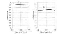
- FIG. 5 is a cross-sectional view showing still another configuration example of the front plane in the ⁇ LED-UV source 1000. It is sectional drawing which shows typically how the ultraviolet rays are reflected by a metal plug 24. It is another cross-sectional view schematically showing how ultraviolet rays are reflected by a metal plug 24. It is a graph which shows the relationship between the reflectance and the wavelength of the reflector metal in the embodiment of this disclosure.
- the "micro LED” in the present disclosure means a light emitting diode (LED) having a size of an occupied area included in a region of 1000 ⁇ m ⁇ 1000 ⁇ m or a striped region having a width of 1000 ⁇ m or less.
- the electromagnetic wave emitted by the micro LED in the present disclosure is ultraviolet light having a wavelength of 380 nm or less.
- ⁇ LED light emitting diode
- the ⁇ LED has a first conductive type first semiconductor layer and a second conductive type second semiconductor layer.
- the first conductive type is one of the p-type and the n-type
- the second conductive type is the other of the p-type and the n-type.
- the first conductive type is p-type
- the second conductive type is n-type
- the first conductive type is n-type
- the second conductive type is p-type.
- Each of the first semiconductor layer and the second semiconductor layer may have a single layer structure or a multilayer structure.
- a light emitting layer having at least one quantum well (or double heterostructure) is formed between the first semiconductor layer and the second semiconductor layer.
- the "micro LED ultraviolet radiation source ( ⁇ LED-UV source)" in the present disclosure is a device including a plurality of ⁇ LEDs, each of which emits ultraviolet rays.
- a plurality of ⁇ LEDs in a ⁇ LED-UV source may be referred to as a “ ⁇ LED array”.
- the ⁇ LED-UV source can be used in various applications requiring ultraviolet irradiation, such as UV curing of resins, exposure of resists, and sterilization.
- the ⁇ LED-UV source of the present disclosure can realize an arbitrary irradiation pattern without a mask.
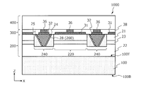
- FIG. 1A is a cross-sectional view showing a part of the ⁇ LED-UV source 1000.
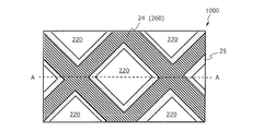
- FIG. 1B is a plan view showing an arrangement example of the ⁇ LED array in the ⁇ LED-UV source 1000.
- the cross section of the ⁇ LED-UV source 1000 shown in FIG. 1A corresponds to the cross section taken along line AA of FIG. 1B.
- the ⁇ LED-UV source 1000 may include a large number of ⁇ LEDs, for example, hundreds to thousands, or more than 10,000. 1A and 1B show only a portion of the ⁇ LED-UV source 1000 containing a few ⁇ LEDs. The entire ⁇ LED-UV source 1000 comprises a configuration in which the illustrated portions are arranged, for example, periodically or in a particular pattern.
- the ⁇ LED-UV source 1000 ultraviolet rays are radiated from a plurality of ⁇ LEDs divided into small pieces, instead of radiating ultraviolet rays from one continuous light emitting layer included in one large conventional LED element. Therefore, how to utilize the ultraviolet radiation from the end face of the light emitting layer contained in each ⁇ LED becomes important. This is because as the size of the ⁇ LEDs decreases and the number of ⁇ LEDs contained in the ⁇ LED-UV source 1000 increases, the ratio of the area of the end face to the area perpendicular to the stacking direction of the semiconductor layers in the light emitting layer increases. In the embodiment of the present disclosure, by providing the reflector described later in the region between the individual ⁇ LEDs (element separation region), it is possible to effectively utilize the ultraviolet rays radiated laterally from the light emitting layer.
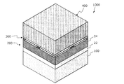
- the ⁇ LED-UV source 1000 includes a crystal growth substrate 100, a front plane 200 supported by the crystal growth substrate 100, an intermediate layer 300 supported by the front plane 200, and a backplane 400 supported by the intermediate layer. ing.
- each component such as ⁇ LED does not necessarily reflect the actual ratio in the embodiment.
- each component is described in a ratio that prioritizes clarity.
- the orientation of each component in the drawing does not limit the orientation when the ⁇ LED-UV source is actually manufactured and the orientation when used.
- FIGS. 1A and 1B show coordinate axes of the X-axis, Y-axis, and Z-axis that are orthogonal to each other.
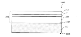
- the crystal growth substrate 100 is a substrate on which semiconductor crystals constituting the ⁇ LED grow epitaxially.
- the crystal growth substrate 100 is a sapphire substrate.
- the crystal growth substrate 100 formed of sapphire is simply referred to as a "substrate”.
- the surface 100T on which crystal growth occurs on the substrate 100 is referred to as an "upper surface” or “crystal growth surface”, and the surface 100B on the opposite side of the substrate 100 is referred to as a "lower surface”.
- the terms “top” and “bottom” are used independently of the actual orientation of the substrate 100.
- a typical example of a semiconductor crystal that can be used in the embodiment of the present disclosure is a gallium nitride based compound semiconductor.
- the gallium nitride based compound semiconductor may be referred to as “GaN”.
- a part of the gallium (Ga) atom in GaN may be replaced by an aluminum (Al) atom or an indium (In) atom.
- GaN in which a part of Ga atom is replaced with Al atom may be referred to as "AlGaN”.
- GaN in which a part of Ga atom is replaced with In atom may be referred to as "InGaN".
- GaN in which a part of Ga atom is replaced with Al atom and In atom may be referred to as "AlInGaN” or “InAlGaN".
- the bandgap of GaN is smaller than the bandgap of AlGaN and larger than the bandgap of InGaN.
- gallium nitride based compound semiconductors in which some of the constituent atoms are replaced with other atoms may be generically referred to as “GaN”.
- GaN can be doped with n-type impurities and / or p-type impurities as impurity ions.
- the semiconductor crystal constituting the ⁇ LED is not limited to the GaN-based semiconductor, and may be formed of a nitride semiconductor such as AlN, InN, or AlInN, or another semiconductor.
- the substrate 100 is a component of the final ⁇ LED-UV source 1000.
- the thickness of the substrate 100 can be, for example, 30 ⁇ m or more and 1000 ⁇ m or less, preferably 500 ⁇ m or less.
- the role of the substrate 100 is to serve as a base for crystal growth and to be an optical member for improving the ultraviolet extraction efficiency during operation. Therefore, the rigidity of the ⁇ LED-UV source 1000 may be supplemented by a rigidity member other than the substrate 100.
- a rigid member can be fixed to, for example, the backplane 400.
- a support substrate (not shown) that supplements the rigidity of the substrate 100 may be fixed to the lower surface 100B of the substrate 100. Such a support substrate can be removed from the final ⁇ LED-UV source 1000.
- the upper surface (crystal growth surface) 100T of the substrate 100 may be provided with a structure such as a groove or a ridge that alleviates the crystal lattice strain. Further, a buffer layer for reducing crystal lattice distortion may be formed on the upper surface 100T of the substrate 100.
- the lower surface 100B of the substrate 100 may be formed with fine irregularities for further improving the extraction efficiency of ultraviolet rays radiated from the ⁇ LED array and transmitted through the substrate 100, or for diffusing the ultraviolet rays. Examples of fine irregularities include a moth-eye structure. Since the moth-eye structure continuously changes the effective refractive index on the lower surface 100B of the substrate 100, the ratio (reflectance) reflected inside the substrate 100 on the lower surface 100B of the substrate 100 is significantly reduced (substantially). Can be zero).
- the positive direction of the Z axis (direction of the arrow) shown in FIG. 1A may be referred to as “crystal growth direction” or “semiconductor lamination direction”.
- the lower surface 100B and the upper surface 100T of the substrate 100 may be referred to as “front” and “back” of the substrate 100, respectively.
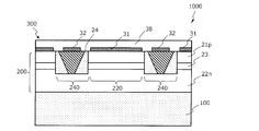
- the front plane 200 includes a plurality of ⁇ LEDs 220 and an element separation region 240 located between the plurality of ⁇ LEDs 220.
- the plurality of ⁇ LED 220s can be arranged in rows and columns in a two-dimensional plane (XY plane) parallel to the upper surface 100T of the substrate 100.
- Each of the plurality of ⁇ LED 220s has a first conductive type first semiconductor layer 21 and a second conductive type second semiconductor layer 22, as shown in FIG. 1A.
- the second semiconductor layer 22 is located closer to the substrate 100 than the first semiconductor layer 21.
- each ⁇ LED 220 has a light emitting layer 23 capable of emitting light independently of the other ⁇ LED 220.
- the light emitting layer 23 is located between the first semiconductor layer 21 and the second semiconductor layer 22.
- the element separation region 240 has at least one metal plug 24 electrically connected to the second semiconductor layer 22.
- the metal plug 24 functions as a substrate-side electrode of the ⁇ LED 220.
- a typical example of the first conductive type first semiconductor layer 21 is a p-GaN layer.
- a typical example of the second conductive type second semiconductor layer 22 is an n-GaN layer.
- the p-GaN layer and the n-GaN layer do not have to have the same composition along the direction perpendicular to the upper surface 100T of the substrate 100 (semiconductor stacking direction: positive direction of the Z axis), and have a multilayer structure.
- Ga in GaN can be at least partially replaced by Al and / or In. Such substitutions may be made to adjust the bandgap and / or index of refraction of the GaN.
- the concentrations of n-type impurities and p-type impurities, that is, the doping levels need not be uniform along the semiconductor stacking direction (positive direction of the Z axis).
- a typical example of the light emitting layer 23 includes at least one AlGaN or InAlGaN well layer because it emits ultraviolet rays.
- a barrier layer having a band gap larger than that of the well layer may be arranged between the well layers.
- the bandgap of the AlGaN well layer can be adjusted according to the Al composition ratio in the AlGaN well layer.
- the plurality of semiconductor layers constituting each ⁇ LED 220 are single crystal layers (epitaxial layers) epitaxially grown on the substrate 100, respectively.
- the element separation region 240 is defined by a trench-shaped recess (hereinafter, referred to as “trench”) formed by partially etching a plurality of semiconductor layers epitaxially grown on the substrate 100.
- the occupied area of each ⁇ LED 220 separated by the trench has a size (eg, 100 ⁇ m ⁇ 100 ⁇ m area or less) contained within the 1000 ⁇ m ⁇ 1000 ⁇ m area.
- the occupied area of the ⁇ LED 220 is defined by the contour of the first semiconductor layer 21 and / or the light emitting layer 23 divided by the element separation area 240.
- the element separation region 240 surrounds each ⁇ LED 220 and separates each ⁇ LED 220 from the other ⁇ LED 220. More specifically, the element separation region 240 electrically and spatially separates the first semiconductor layer 21 and the light emitting layer 23 of each ⁇ LED 220 from the first semiconductor layer 21 and the light emitting layer 23 of the other ⁇ LED 220. ing.
- the second semiconductor layer 22 does not have to be completely separated for each ⁇ LED 220.
- the second semiconductor layer 22 included in each of the plurality of ⁇ LED 220s is formed of one continuous semiconductor layer and is shared by the plurality of ⁇ LED 220s.
- the second semiconductor layer 22 functions as a common electrode on the second conductive side with respect to the plurality of ⁇ LEDs 220.
- the second semiconductor layer 22 of each ⁇ LED 220 is separated from each other and the second semiconductor layer 22 is individually connected to the electrode (wiring) on the second conductive side in the backplane 400, the second conductive If a disconnection defect occurs in a part of the electrode or the wiring on the side, an energization failure occurs in a part of the ⁇ LED 220.
- the second semiconductor layer 22 of each of the plurality of ⁇ LED 220s is formed of one continuous semiconductor layer, the occurrence of such defects can be suppressed.
- the embodiments of the present disclosure are not limited to such examples.
- the second semiconductor layer 22 of each ⁇ LED 220 may be separated from the second semiconductor layer 22 of the other ⁇ LED 220 as long as it is appropriately connected to the metal plug 24, the TiN buffer layer described later, or the like.
- the element separation region 240 has an embedded insulator 25 that fills the space between the plurality of ⁇ LEDs 220.
- the embedded insulator 25 has one or more through holes for the metal plug 24. The through holes are filled with the metal material constituting the metal plug 24.
- the metal plug 24 may have a structure in which different metal layers are stacked.
- the upper surface of the front plane 200 is flattened as shown in FIG. 1A.
- Such flattening is realized by the level of the upper surface of the metal plug 24 and the embedded insulator 25 in the element separation region 240 substantially matching the level of the upper surface of the first semiconductor layer 21 in the ⁇ LED 220.
- the element separation region 240 of the ⁇ LED-UV source 1000 includes a reflector 260 that reflects ultraviolet rays emitted from each of the plurality of ⁇ LED 220s toward the crystal growth substrate 100. More specifically, the element separation region 240 has an embedded insulator 25 that fills the space between the plurality of ⁇ LEDs 220, and the embedded insulator 25 has a V-shaped groove (through hole) for the metal plug 24. Have. The embedded insulator 25 is formed of a material that transmits ultraviolet rays emitted from the ⁇ LED 220.
- the metal plug 24 is in contact with the second semiconductor layer 22 at the bottom of the V-shaped groove.
- the metal plug 24 not only functions as a conductor for electrically connecting each ⁇ LED 220 to the backplane 400, but also functions as a reflector 260.
- the side surface (reflection surface 260S) of the metal plug 24 is not orthogonal to the upper surface 100T of the crystal growth substrate 100 and is inclined. It is desirable that the metal plug 24 is formed of a material that realizes ohmic contact at least in a portion that contacts the second semiconductor layer 22. However, other parts can be formed from various metallic materials.
- the metal plug 24 is Al. It is desirable that it is formed from.
- the reflecting surface 260S of the reflector 260 is preferably formed of Al, Ag or Rh.
- Al or Rh is desirable as the reflecting surface 260S of the reflector 260 for ultraviolet rays having a wavelength of 300 nm or less.
- the reflectance of ultraviolet rays having a wavelength of 350 nm has a relationship of Al> Ag> Rh >> Cu ⁇ Ti.
- the reflectance of ultraviolet rays having a wavelength of 300 nm or less has a relationship of Al> Rh >> Ti> Cu> Ag.
- the metal plug 24 which functions as the reflector 260, surrounds each ⁇ LED 220, as shown in FIG. 1B. Therefore, the ultraviolet rays radiated from the ⁇ LED 220 in all directions are reflected in the direction of the crystal growth substrate 100 by the inclined side surface (reflection surface 260S) of the metal plug 24.
- the metal plug 24 does not have to be a single conductor having a lattice shape, and may be separated into a plurality of portions.
- the metal plug 24 has a reflective layer 28 on the side surface, and the reflective layer 28 functions as a reflector 260.
- the reflective layer 28 may be formed of a material different from that of the metal plug 24, such as Al or Rh.
- the thickness of the reflective layer 28 is, for example, 30 nm or more and 50 nm or less.
- the reflective layer 28 may be formed of a material other than metal.
- the reflective layer 28 may be formed, for example, from a dielectric material having a refractive index different from that of the embedded insulator 25.
- Ultraviolet rays radiated from the ⁇ LED 220 can be reflected by utilizing the difference in refractive index existing at the interface between the reflective layer 28 and the embedded insulator 25. Ultraviolet rays that have passed through this interface and entered the metal plug 24 can be reflected by the metal plug 24 itself.
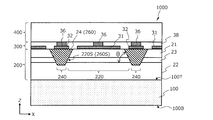
- FIG. 3 is a cross-sectional view showing another configuration example of the ⁇ LED-UV source 1000.
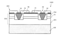
- Each of the plurality of ⁇ LEDs 220 in this example has an inclined side surface 220S.
- the metal plug 24 is in contact with the side surface 220S of each ⁇ LED 220.
- the metal plug 24 has a reflective surface 260S that contacts the side surface 220S of each ⁇ LED 220 and functions as a reflector 260.
- the tilt angle ⁇ of the reflective surface 260S defines the tilt angle of the side surface 220S of each ⁇ LED 220.
- the inclination angle ⁇ of the reflecting surface 260S is less than 90 degrees (for example, 30 to 60 degrees).
- the side surface 220S of the ⁇ LED 220 forms a forward taper.
- the surface of the metal plug 24 is preferably formed of a material capable of achieving ohmic contact with the second semiconductor layer 22.
- the second semiconductor layer 22 is formed of n-GaN
- the second semiconductor layer 22 and the metal plug 24 are formed by using a metal (for example, Ti) having a work function ⁇ m smaller than the work function ⁇ n of n-GaN.
- a high resistance layer can be formed between the first semiconductor layer 21 formed of p-GaN and the metal plug 24.
- the step of forming the embedded insulator 25 in the element separation region 240 and the step of forming the through hole in the embedded insulator 25 can be omitted.
- the configuration of the metal plug 24 is not limited to the above example, and may have a laminated structure (upper layer metal and lower layer metal).
- the material of the upper metal is selected so that a high resistance or insulating interface is formed between the upper metal and the first semiconductor layer 21, and the material of the upper metal is low between the lower metal and the second semiconductor layer 22.
- the material of the underlying metal is selected so that a resistant ohmic contact is formed. At this time, as described below, it is preferable that a material having a high reflectance to ultraviolet rays is in contact with at least the light emitting layer 23.
- the first semiconductor layer 21 is formed of p-GaN, it is generally difficult to form ohmic contact, and the resistance due to etching due to element separation is the resistance between p-GaN and the metal plug 24. To form. Therefore, as shown in FIG. 3, the problem that the first semiconductor layer 21 and the second semiconductor layer 22 are electrically short-circuited by the metal plug 24 is avoided.
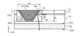
- ⁇ Reflector tilt angle and material> 4A and 4B schematically show how the ultraviolet rays generated in the light emitting layer 23 are reflected by the metal plug 24.
- the high reflectance layer 24R is provided in the region of the metal plug 24 that reflects ultraviolet rays.
- the high reflectance layer 24R functions as a reflector 260.
- Ultraviolet rays generated in the light emitting layer 23 in the ⁇ LED are basically emitted isotropically, but are radiated laterally along the light emitting layer 23 having a relatively large bandgap and a high refractive index. Cheap. Therefore, the inclination angle of the reflector 260 with respect to the light emitting layer 23 is important in order to realize high reflectance and to allow ultraviolet rays to enter the substrate 100 at an appropriate angle.
- the reflecting surface 260S of the reflector 260 shown in FIGS. 4A and 4B reflects the ultraviolet rays received from the light emitting layer 23 downward (in the negative direction of the Z axis).
- the ultraviolet rays reflected by the reflecting surface 260S travel in a direction forming an angle of
- degrees with respect to the negative direction of the Z axis will be referred to as the "board incident angle".
- the side surfaces of the semiconductor layers 21, 22, and 23 are inclined at an inclination angle ⁇ to form a forward taper.
- the incident angle of the substrate is 25 degrees or less in order to realize the light extraction of ultraviolet rays, preferably 15. It was found that the temperature was less than or equal to 10 degrees, more preferably 10 degrees or less. Therefore, the inclination angle ⁇ of the reflecting surface 260S of the reflector 260 needs to be in the range of 32.5 to 57.5 degrees, and the angle ⁇ is preferably 37.5 to 52.5 degrees. It is preferably in the range of 40 to 50 degrees.
- the angle ⁇ is in the range of 40 to 50 degrees, a high light extraction efficiency of about 90% is realized.
- the substrate 100 is made of sapphire and not when it is made of another material, such as GaN.
- ultraviolet rays having a wavelength of 375 nm or less cannot be extracted even if the substrate incident angle is 0 degrees.
- a titanium nitride (TiN) layer may be formed on the upper surface 100T of the substrate 100.
- the TiN layer contributes to crystal growth, but affects the transmission of ultraviolet light. According to the study of the present inventor, if the incident angle of the substrate is 23 degrees or less, ultraviolet rays can be extracted.
- the substrate incident angle is preferably 10 degrees or less. When the substrate incident angle is 10 degrees or less, a light extraction efficiency of 60% or more can be realized.
- the material of the reflective surface 260S of the metal plug 24 (reflector 260) is preferably Al or Rh, which has a high reflectance with respect to ultraviolet rays.
- the inside of the metal plug 24 (reflector 260) may be formed of other metals such as Cu, Ag, Ti, TiN and the like. It was also found that the ultraviolet reflectance tends to increase as the Al layer or the Rh layer becomes thicker up to about 50 nm.
- the preferred thickness of the Al layer or Rh layer that functions as a reflector is, for example, 30 nm or more.
- a metal showing a relatively high reflectance in the wavelength range of visible light can be a metal other than Al and Rh in the wavelength range of 200 nm or more and 300 nm or less used for sterilization, for example. It was found that the reflectance was significantly reduced.
- the reflectance of Al has a wide wavelength of 200 to 380 nm as shown in FIG. 4C. In the range, it is almost 90% or more.
- the reflectance of Rh is also about 68% or more in a wide range of wavelengths of 200 to 380 nm.
- the reflectance of Ag is about 85% at a wavelength of 350 nm, but decreases to 37% at a wavelength of 295 nm, as shown in FIG. 4D.
- the reflectance of Cu is 50% or more at a wavelength of 380 nm and about 40% at a wavelength of 260 to 280 nm. Comparing Cu and Ag in detail, the reflectance in the wavelength range of 200 nm to 280 nm is Cu ⁇ Ag, whereas the reflectance in the wavelength range of 280 nm to 305 nm is Cu> Ag, and when it exceeds 305 nm, Ag >> Cu. It becomes.
- Ag is preferable in the region where the wavelength is larger than 305 nm
- Cu is preferable in the region where the wavelength is around 300 nm.
- Al exhibits a higher reflectance than Ag and Cu in the entire wavelength range.
- Rh is lower than Ag at 318 nm or more, but exhibits higher reflectance than Ag and Cu at other temperatures of 300 nm or less.
- the ⁇ LED ultraviolet radiation light source of the present disclosure when used for sterilization (wavelength: 200 nm or more and 300 nm or less, typically 250 nm or more and 300 nm or less), at least the reflecting surface 260S of the reflector 260 It is preferably formed from Al or Rh.
- the layer thickness of Al or Rh constituting the reflective surface 260S is about 30 nm or more. Even if this layer thickness is increased to 50 nm or more, the increase in reflectance is saturated. Therefore, the layer thickness of Al or R in the portion that functions as the reflector 260 is preferably 30 to 50 nm.
- another metal is selected from the viewpoint of reducing electrical resistivity or contact resistance without considering ultraviolet reflectance. can do.
- the contact portion of the metal plug 24 it is preferable to use TiN for the contact portion of the metal plug 24, but when the TiN layer is present on the reflective surface 260S, the reflectance with respect to ultraviolet rays is lowered.
- the angle ⁇ is preferably 40 degrees or less. The smaller each ⁇ , the better the reflectance.
- the size (width W) of the metal plug 24 (reflector 260) in the X-axis direction (or Y-axis direction) may be larger than the size (height h) of the metal plug 24 in the Z-axis direction.
- a typical example of the width ratio (W / h) to the height of the metal plug 24 can be 0.5 or more and 10 or less.
- the cross section of the metal plug 24 (reflector 260) of FIGS. 4A and 4B has an inverted trapezoidal shape or an inverted triangular shape, and the cross-sectional shape of the metal plug 24 (reflector 260) is such an example.
- the side surface 220S of each ⁇ LED 220 does not have to be flat.
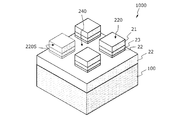
- FIG. 5 is a perspective view showing an example in which the side surface 220S of the ⁇ LED 220 is formed from the side surface of the truncated cone.
- the shape of each ⁇ LED 220 can be formed from any frustum with a polygonal, circular or elliptical bottom.
- FIG. 6 is a cross-sectional view showing still another configuration example of the ⁇ LED-UV source 1000.
- Each of the plurality of ⁇ LED 220s in this example also has a forward tapered side surface 220S.
- the metal plug 24 is not in contact with the side surface 220S of each ⁇ LED.
- the metal plug 24 is located in a through hole formed in the embedded insulator 25.
- the reflector 260 that reflects the ultraviolet rays emitted from each ⁇ LED 220 toward the crystal growth substrate 100 is the interface (side surface 220S) between the embedded insulator 25 and the ⁇ LED 220.
- Such interfacial reflection is Fresnel reflection caused by the difference between the refractive index of the embedded insulator 25 and the refractive index of ⁇ LED 220.
- the refractive index of the semiconductor that can form the ⁇ LED 220 is, for example, in the range of 2.1 or more and 3.0 or less.
- the embedded insulator 25 is formed from a dielectric having a refractive index lower than these refractive indexes, it is possible to generate total reflection of the ultraviolet rays emitted from the light emitting layer 23 by adjusting the inclination angle of the reflecting surface. Is.
- the refractive index of the embedded insulating material 25 may be higher than that of the ⁇ LED 220.
- FIG. 7 is a cross-sectional view showing still another configuration example of the ⁇ LED-UV source 1000.
- Each of the plurality of ⁇ LED 220s in this example also has a forward tapered side surface 220S.
- the reflector 260 is formed of a reflective layer 28 in contact with the side surface 220S of the ⁇ LED 220.
- the reflective layer 28 may be a dielectric multilayer film in which a plurality of dielectric layers having different refractive indexes are alternately laminated.
- the reflectance of the dielectric multilayer film can be set to 95% or more by adjusting the film thickness of each and laminating them for 5 cycles or more.
- Such ultraviolet rays can be used for various purposes.
- the intermediate layer 300 includes a plurality of first contact electrodes 31 and a second contact electrode 32 (see FIG. 1A). Each of the plurality of first contact electrodes 31 is electrically connected to the first semiconductor layer 21 of the plurality of ⁇ LED 220s. At least one second contact electrode 32 is connected to the metal plug 24.
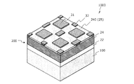
- FIG. 8 is a perspective view showing an arrangement example of the first contact electrode 31 and the second contact electrode 32.
- the description of the backplane 400 is omitted.
- the structure shown in FIG. 8 is only a part of the ⁇ LED-UV source 1000, and as described above, the embodiment of the ⁇ LED-UV source 1000 includes a large number of ⁇ LED 220s.
- the second contact electrode 32 shown in FIG. 8 is electrically connected to the second semiconductor layer 22 via the metal plug 24.
- the shape and size of the second contact electrode 32 are not limited to the examples shown. As described above, since the metal plug 24 can take various shapes, the degree of freedom in arranging the second contact electrode 32 is high as long as it is electrically connected to the second semiconductor layer 22 via the metal plug 24.
- the first contact electrode 31 is independently electrically connected to the first semiconductor layer 21 of the plurality of ⁇ LED 220s. When viewed from a direction perpendicular to the upper surface 100T of the substrate 100, the shape and size of the first contact electrode 31 need not match the shape and size of the first semiconductor layer 21.
- the distance from the substrate 100 to the first contact electrode 31 and the second contact electrode 32 in other words, the “height” of these contact electrodes 31 and 32.
- “Or” level are equal to each other. This facilitates the formation of the backplane 400, which will be described later, using semiconductor manufacturing technology.
- the "semiconductor manufacturing technique" in the present disclosure includes a step of depositing a thin film of a semiconductor, an insulator, or a conductor, and a step of patterning the thin film by a lithography and etching steps.
- the "flattened surface” means a surface having a step difference of 300 nm or less due to a convex portion or a concave portion existing on the surface. In a preferred embodiment, this step is 100 nm or less.
- the intermediate layer 300 includes an interlayer insulating layer 38 having a flat surface.
- the interlayer insulating layer 38 has a plurality of contact holes for connecting the first and second contact electrodes 31 and 32 to the electric circuit of the backplane 400, respectively.
- the contact hole is filled with the via electrode 36.
- CMP chemical mechanical polishing
- the backplane 400 has an electrical circuit (not shown) in FIG. 1A.
- the electric circuit is electrically connected to the plurality of ⁇ LED 220s via the plurality of first contact electrodes 31 and at least one second contact electrode 32.
- the electrical circuit comprises a plurality of thin film transistors (TFTs) and other circuit elements.
- TFTs thin film transistors
- each of the TFTs has a semiconductor layer grown on the front plane 200 and / or the intermediate layer 300 supported by the substrate 100.
- TFTs thin film transistors
- each of the TFTs has a semiconductor layer grown on the front plane 200 and / or the intermediate layer 300 supported by the substrate 100.
- the electrical circuit of the backplane 400 does not need to include a TFT.
- the electrical circuit of the backplane 400 does not include a TFT
- the electrical circuit is made of metal, semiconductor, and / or insulating material grown directly on the intermediate layer 300 by physical or chemical vapor deposition. Contains layers (growth or sedimentary layers). These layers are patterned by lithographic techniques.
- FIG. 9 is a basic equivalent circuit diagram when the ⁇ LED-UV source 1000 emits ultraviolet rays in units of ⁇ LED.
- the electric circuit of the backplane 400 has a selection TFT element Tr1, a driving TFT element Tr2, and a holding capacitance CH.
- the ⁇ LED shown in FIG. 9 resides in the front plane 200 rather than in the backplane 400.
- the selection TFT element Tr1 is connected to the intensity signal line DL and the selection line SL.
- the intensity signal line DL is a wiring that carries a signal that defines the intensity of ultraviolet radiation.
- the intensity signal line DL is electrically connected to the gate of the driving TFT element Tr2 via the selection TFT element Tr1.
- the selection line SL is a wiring that carries a signal for controlling on / off of the selection TFT element Tr1.
- the driving TFT element Tr2 controls the conduction state between the power line PL and the ⁇ LED. When the driving TFT element Tr2 is turned on, a current flows from the power line PL to the ground line GL via the ⁇ LED. This current causes the ⁇ LED to emit light. Even if the selection TFT element Tr1 is turned off, the driving TFT element Tr2 is maintained in the ON state due to the holding capacitance CH.
- the backplane 400 having the above configuration, it is possible to control the radiation intensity of ultraviolet rays in units of ⁇ LED.
- the intensity distribution of ultraviolet irradiation can be easily changed according to the input intensity signal.
- the electric circuit of the backplane 400 may include a selection TFT element Tr1, a drive TFT element Tr2, an intensity signal line DL, a selection line SL, and the like, but the configuration of the electric circuit is not limited to such an example.
- FIG. 10A a substrate 100 having an upper surface (crystal growth surface) 100T is prepared.
- FIG. 10A shows only a part of the substrate 100 extending along a plane parallel to the upper surface 100T.
- Each semiconductor layer is a single crystal epitaxial growth layer of a gallium nitride based compound semiconductor.
- the gallium nitride based compound semiconductor can be grown by, for example, the MOCVD (Metal Organic Chemical Vapor Deposition) method. Impurities defining each conductive type can be doped from the gas phase during crystal growth.
- the mask M1 is formed on the first semiconductor layer 21 as shown in FIG. 10B.
- the mask M1 has an opening that defines the shape and position of the element separation region 240.
- the mask M1 defines the shape and position of the ⁇ LED 220.
- a trench defining the element separation region 240 is formed by etching the portion of the semiconductor laminated structure 280 that is not covered by the mask M1 from the upper surface. This etching (mesa etching) can be performed by, for example, an inductively coupled plasma (ICP) etching method or a reactive ion etching (RIE) method.
- ICP inductively coupled plasma
- RIE reactive ion etching
- the etching depth is determined so that the second semiconductor layer 22 appears at the bottom of the trench.
- the depth of the trench formed by etching can be, for example, 0.5 ⁇ m or more and 5 ⁇ m or less, and the width of the trench can be, for example, 5 ⁇ m or more and 100 ⁇ m or less. From the viewpoint of increasing the in-plane uniformity of the ultraviolet irradiation intensity, the width of the trench is preferably small.
- the width of each ⁇ LED 220 can be, for example, 5 ⁇ m or more and 1000 ⁇ m or less, for example, 10 to 100 ⁇ m.
- each two-dimensionally arranged ⁇ LED 220 is reduced (for example, within a region of 100 ⁇ m ⁇ 100 ⁇ m or less, or a width of 100 ⁇ m. It is preferable that the size fits within the stripe area of.
- the side surface 220S of the ⁇ LED 220 is exposed by etching. In other words, each ⁇ LED 220 has etched side surfaces 220S. In the example of FIG. 10C, the side surface 220S is not inclined, but the above-mentioned forward taper can be formed by adjusting the material and etching conditions of the mask M1.
- the first contact electrode 31 and the second contact electrode 32 are formed as shown in FIG. 8 described above.
- the interlayer insulating layer (thickness: 500 nm to 1500 nm) 38 of the intermediate layer 300 a plurality of contact holes for connecting the electric circuit of the backplane 400 to the ⁇ LED 220 of the frontplane 200 (in FIG. 8). (Not shown) is formed on the interlayer insulating layer 38.
- the contact hole is formed so as to reach the contact electrodes 31 and 32 located in the lower layer.
- the contact hole is filled with via electrodes.
- the upper surface of the interlayer insulating layer 38 can be smoothed by CMP treatment.
- the backplane 400 is formed on the intermediate layer 300.
- the characteristic point in the present disclosure is that the backplane 400 is not attached on the intermediate layer 300, but the various electronic elements and wirings constituting the backplane 400 are mounted on the front plane 200 and the intermediate layer 300 by semiconductor manufacturing technology. It is to be formed directly on the laminated structure containing.
- each of the plurality of TFTs included in the backplane 400 has a semiconductor layer grown on a laminated structure composed of a front plane 200 and an intermediate layer 300 supported by the substrate 100.
- the backplane 400 including the TFT when the upper surface of the front plane 200 and the upper surface of the intermediate layer 300 are flattened, it becomes easy to manufacture the backplane 400 including the TFT by the semiconductor manufacturing technology.
- a TFT is formed by a semiconductor manufacturing technique, it is necessary to pattern the deposited semiconductor layer, insulating layer, and metal layer. Such patterning is realized by a lithography process involving exposure. If there is a large step on the base of the deposited semiconductor layer, insulating layer, and metal layer, the focus will not be achieved during exposure, and highly accurate fine patterning will not be realized.
- the intermediate layer 300 is also flattened, and the backplane 400 can be easily formed by the semiconductor manufacturing technique.
- the shape of the ⁇ LED 220 is substantially a rectangular parallelepiped, but the shape of the ⁇ LED 220 may be a cylinder, a polygonal column such as a hexagonal column, or an ellipse. It may be a pillar. Further, as shown in FIG. 4B, it may have an inclined side surface.
- the ⁇ LED-UV source 1000 in the present embodiment is an ultraviolet radiation source having the same configuration as the above-mentioned basic configuration example.
- the ⁇ LED-UV source 1000 is formed on a substrate 100 formed of sapphire, a front plane 200 formed on the substrate 100, an intermediate layer 300 formed on the front plane 200, and an intermediate layer 300. It is equipped with a backplane 400.
- the substrate 100 is placed in the reaction chamber of the MOCVD apparatus, and various gases are supplied to perform epitaxial growth of the gallium nitride (GaN) -based compound semiconductor.
- the substrate 100 in this embodiment is, for example, a sapphire substrate having a thickness of about 50 to 600 ⁇ m.
- the upper surface 100T of the substrate 100 is typically a C surface (0001), but may have a non-polar surface or a semi-polar surface such as an m surface, an a surface, or an r surface on the upper surface. Further, the upper surface 100T may be inclined by about several degrees from these crystal planes.
- the substrate 100 is typically disc-shaped, and its diameter can be, for example, 1 to 8 inches.
- the shape and size of the substrate 100 are not limited to this example, and may be rectangular. Further, the manufacturing process may be advanced using the disk-shaped substrate 100, and finally the periphery of the substrate 100 may be cut and processed into a rectangular shape. Further, the manufacturing process may be advanced using the relatively large substrate 100, and finally one substrate 100 may be divided to form a plurality of ⁇ LED-UV sources (singulation).
- TMG trimethylgallium
- TAG triethylgallium
- H 2 hydrogen
- N 2 nitrogen
- NH 3 ammonia
- SiH 4 silane Supply.
- the substrate 100 is heated to about 1100 ° C. to grow an n-GaN layer (thickness: for example, 2 ⁇ m) 22n.
- Silane is a raw material gas that supplies Si, which is an n-type dopant.
- the doping concentration of n-type impurities can be, for example, 5 ⁇ 10 17 cm -3 .
- the supply of SiH 4 is stopped, and the temperature of the substrate 100 is lowered to less than 800 ° C. to form the light emitting layer 23. More specifically, first, Al x In y Ga z N (0 ⁇ x ⁇ 1,0 ⁇ y ⁇ 1,0 ⁇ z ⁇ 1) growing a barrier layer. Further starts supply of trimethylindium (TMI) Al x 'In y ' Ga z 'N (0 ⁇ x' ⁇ 1,0 ⁇ y' ⁇ 1,0 ⁇ z' ⁇ 1) is grown the well layer. By alternately growing the barrier layer and the well layer in two or more cycles, a light emitting layer (thickness: for example, 100 nm) 23 having multiple quantum wells functioning as a light emitting portion can be formed.
- TMI trimethylindium
- One light emitting layer 23 may have a single well layer sandwiched between two barrier layers.
- a well layer may be formed directly on the n-GaN layer 22n, and a barrier layer may be formed on the well layer.
- TMI trimethylaluminum
- Mg trimethylaluminum
- Pentazienyl magnesium (Cp 2 Mg) may be supplied to grow the overflow suppression layer.
- the supply of TMA is stopped, and the p-GaN layer (thickness: for example, 0.5 ⁇ m) 21p is grown.
- the doping concentration of p-type impurities can be, for example, 5 ⁇ 10 17 cm -3 .
- An n-AlGaN layer may be provided between the n-GaN layer 22n and the light emitting layer 23, or an n-AlGaN layer may be used instead of the n-GaN layer 22n. Further, a p-AlGaN layer may be formed between the light emitting layer 23 and the p-GaN layer 21p.
- predetermined regions (element separation region 240) of the p-GaN layer 21p and the light emitting layer 23 are performed. (For example, 1.5 ⁇ m) is removed to expose a part of the n-GaN layer 22n. Etching of the gallium nitride based semiconductor can be performed using a chlorine-based gas plasma as described later.
- the space defining the element separation region 240 is filled with the embedded insulating material 25.
- the material and the forming method of the embedded insulating material 25 are arbitrary as long as they are selected from the material transmitting ultraviolet rays and the forming method thereof.
- the top surface of the embedded insulator 25 is flattened and located at the same level as the top surface of the p-GaN layer 21p.
- a through hole 26 reaching the n-GaN layer 22n is formed in a part of the embedded insulator 25.
- the through hole 26 defines the position and shape of the metal plug 24.
- the side surfaces of the through holes 26 are tilted so that the metal plug 24 functions as a reflector.
- the through hole 26 accommodates a metal plug 24 having a shape as shown in FIG. 1B.
- a metal plug 24 that fills the through hole 26 is formed, and the upper surface of the front plane 200 is flattened. After that, the first contact electrode 31 and the second contact electrode 32 are formed. Flattening can be done by various processes such as etchback, selective growth, or lift-off.
- the metal plug 24 makes ohmic contact with the n-GaN layer 22n, it can be formed of a metal such as titanium (Ti) and / or aluminum (Al).
- the metal plug 24 preferably has a metal layer containing Ti (for example, a TiN layer) at a portion in contact with the n—GaN layer 22n.
- Ti titanium
- Al aluminum
- the presence of the TiN layer contributes to the realization of low resistance n-type ohmic contact.
- the TiN layer can be formed by forming a Ti layer in contact with the n—GaN layer 22n and then performing a heat treatment at, for example, about 600 ° C. for 30 seconds. As described above, it is desirable that Al or Rh is present in the portion that reflects ultraviolet rays.
- the first and second contact electrodes 31 and 32 can be formed by depositing and patterning a metal layer.
- a metal-semiconductor interface is formed between the first contact electrode 31 and the p-GaN layer 21p of the ⁇ LED 220.
- the material of the first contact electrode 31 can be selected from metals with a high work function, such as platinum (Pt) and / or palladium (Pd). After forming the Pt or Pd layer (thickness: about 50 nm), heat treatment can be performed, for example, at a temperature of 350 ° C. or higher and 400 ° C. or lower for about 30 seconds.
- a Pt or Pd layer is present in the portion that is in direct contact with the p-GaN layer 21p, another metal such as a Ti layer (thickness: about 50 nm) and / or an Au layer (thickness: about 50 nm) and / or Au layer Thickness: about 200 nm) may be laminated.
- a region in which p-type impurities are doped at a relatively high concentration may be formed on the upper portion of the p-GaN layer 21p.
- the second contact electrode 32 is electrically connected to the metal plug 24 instead of the semiconductor. Therefore, the material of the second contact electrode 32 can be selected from a wide range.
- the first contact electrode 31 and the second contact electrode 32 may be formed by patterning one continuous metal layer. This patterning also includes lift-off. When the thicknesses of the first contact electrode 31 and the second contact electrode 32 are equal to each other, it becomes easy to connect to an electric circuit in the backplane 400 such as the TFT 40 described later.
- first and second contact electrodes 31, 32 After forming the first and second contact electrodes 31, 32, they are covered with an interlayer insulating layer (thickness: for example, 1000 nm to 1500 nm) 38.
- the upper surface of the interlayer insulating layer 38 can be flattened by CMP treatment or the like.
- the thickness of the interlayer insulating layer 38 whose upper surface is flattened means "average thickness".
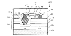
- a contact hole 39 is formed in the interlayer insulating layer 38.
- the contact hole 39 is used to electrically connect the electrical circuit of the backplane 400 to the ⁇ LED 220 of the frontplane 200.
- the TFT 40 is a semiconductor that contacts at least a part of the upper surfaces of the drain electrode 41 and the source electrode 42 formed on the interlayer insulating layer 38 and the drain electrode 41 and the source electrode 42, respectively. It has a thin film 43, a gate insulating film 44 formed on the semiconductor thin film 43, and a gate electrode 45 formed on the gate insulating film 44.
- the drain electrode 41 and the source electrode 42 are connected to the first contact electrode 31 and the second contact electrode 32 by the via electrode 36, respectively.
- the components of these TFTs 40 are formed by known semiconductor manufacturing techniques.
- the semiconductor thin film 43 can be formed from polycrystalline silicon, amorphous silicon, oxide semiconductors, and / or gallium nitride based semiconductors.
- the polycrystalline silicon can be formed, for example, by depositing amorphous silicon on the interlayer insulating layer 38 of the intermediate layer 300 by a thin film deposition technique, and then crystallizing the amorphous silicon with a laser beam.
- the polycrystalline silicon formed in this way is called LTPS (Low-Temperature Poly Silicon).
- the polycrystalline silicon is patterned into the desired shape in the lithography and etching steps.
- the TFT 40 in FIG. 11 is covered with an insulating layer (thickness: for example, 500 nm to 3000 nm) 46.
- the insulating layer 46 is provided with an opening hole (not shown), which makes it possible to connect the TFT 40, for example, the gate electrode 45 to an external driver integrated circuit element or the like. It is preferable that the upper surface of the insulating layer 46 is also flattened.
- the electrical circuit of the backplane 400 may include circuit elements such as TFTs, capacitors, and diodes (not shown). Therefore, the insulating layer 46 may have a structure in which a plurality of insulating layers are laminated, and in that case, each insulating layer may be provided with a via electrode for connecting circuit elements, if necessary. Further, wiring may be formed on each insulating layer as needed.
- the backplane 400 in this embodiment can have the same configuration as a known backplane (for example, a TFT substrate) used in a display device.
- the backplane 400 of the present disclosure is characterized in that it is formed by semiconductor manufacturing technology on the ⁇ LED 220 located in the lower layer. Therefore, for example, the drain electrode 41 and the source electrode 42 of the TFT 40 can be formed by patterning a metal layer deposited so as to cover the front plane 200. Such patterning enables highly accurate alignment by lithographic techniques.
- the front plane 200 and / or the intermediate layer 300 are both flattened, it is possible to increase the resolution of lithography.
- the configuration of the TFT 40 shown in FIG. 11 is an example.
- the drain electrode 41 of the TFT 40 may be another circuit element in the backplane 400 or It may be connected to the wiring.
- the source electrode 42 of the TFT 40 does not need to be electrically connected to the second contact electrode 32.
- the second contact electrode 32 may be connected to a wiring (for example, a ground wiring) that commonly gives a predetermined potential to the n-GaN layer 22n of the ⁇ LED 220.
- the electric circuit of the backplane 400 has a plurality of metal layers (metal layers functioning as the drain electrode 41 and the source electrode 42) connected to the first contact electrode 31 and the second contact electrode 32, respectively. ing.
- the plurality of first contact electrodes 31 each cover the p-GaN layer 21p of the plurality of ⁇ LED 220s and function as a light-shielding layer or a reflective layer.
- the individual first contact electrodes 31 do not have to completely cover the upper surface of the ⁇ LED 220, that is, the entire upper surface of the p-GaN layer 21p.
- the shape, size, and position of the first contact electrode 31 are determined to achieve a sufficiently low contact resistance and to sufficiently suppress the ultraviolet rays emitted from the light emitting layer 23 from entering the channel region of the TFT 40. Will be done. It should be noted that preventing the ultraviolet rays radiated from the light emitting layer 23 from entering the channel region of the TFT 40 can also be realized by arranging another metal layer at an appropriate position.
- the intermediate layer 300 having a flattened upper surface is formed on the front plane 200 having a flat upper surface realized by embedding the element separation region 240 with the metal plug 24 and the embedded insulating material 25.
- These structures (substructures) function as a base for forming circuit elements such as TFTs on the structures.
- the above-mentioned substructure is treated at a temperature of, for example, 350 ° C. or higher.
- the embedded insulating material 25 in the element separation region 240 and the interlayer insulating layer 38 contained in the intermediate layer 300 are formed of a material that does not deteriorate even by heat treatment at 350 ° C. or higher.
- polyimide and SOG Spin-on Glass
- the configuration of the TFT included in the electric circuit in the backplane 400 is not limited to the above example.
- FIG. 13 is a cross-sectional view schematically showing another example of the TFT.
- FIG. 14 is a cross-sectional view schematically showing still another example of the TFT.
- the TFT 40 includes a drain electrode 41, a source electrode 42, and a gate electrode 45 formed on the interlayer insulating layer 38, a gate insulating film 44 formed on the gate electrode 45, and a gate insulating film 44. It has a semiconductor thin film 43 formed on the top and in contact with at least a part of the upper surface of each of the drain electrode 41 and the source electrode 42.
- the drain electrode 41 and the source electrode 42 are connected to the first contact electrode 31 and the second contact electrode 32 by the via electrode 36, respectively.
- the TFT 40 has a semiconductor thin film 43 formed on the interlayer insulating layer 38, and a drain electrode 41 and a source electrode 42 formed on the interlayer insulating layer 38 and in contact with a part of the semiconductor thin film 43, respectively. And a gate insulating film 44 formed on the semiconductor thin film 43, and a gate electrode 45 formed on the gate insulating film 44.
- the drain electrode 41 and the source electrode 42 are connected to the first contact electrode 31 and the second contact electrode 32 by the via electrode 36, respectively.
- the configuration of the TFT 40 is not limited to the above example.
- it in the initial stage of the process of forming the TFT 40, it is connected to the first and second contact electrodes 31 and 32 of the front plane 200 via the contact hole 39 of the interlayer insulating layer 38 in the intermediate layer 300.
- Multiple metal layers are formed. These metal layers can be, but are not limited to, the drain electrode 41 or the source electrode 42 of the TFT 40.
- the drain electrode 41 and the source electrode 42 in this embodiment are patterned by a photolithography and etching step after depositing a metal layer on the interlayer insulating layer 38 in the flattened intermediate layer 300. Therefore, there is no misalignment between the front plane 200 (intermediate layer 300) and the back plane 400 that causes a decrease in yield.
- FIG. 15 is a cross-sectional view schematically showing a part of a ⁇ LED-UV source having a titanium nitride (TiN) layer 50 located between the substrate 100 and the n-GaN layer 22n of each ⁇ LED 220.
- the thickness of the TiN layer 50 can be, for example, 5 nm or more and 20 nm or less.
- the TiN layer 50 can be suitably used in combination with the substrate 100 formed of sapphire.
- the TiN layer 50 has electrical conductivity.
- a large number of ⁇ LED 220s are arranged over a wide range, and at least one metal plug 24 connects the n-GaN layer 22n of the ⁇ LED 220 to the electrical circuit of the backplane 400. Therefore, if the electric resistance component (sheet resistance) with respect to the current flowing from the n-GaN layer 22n to the metal plug 24 is too high, the power consumption will increase.
- the TiN layer 50 functions as a buffer layer for alleviating lattice mismatch during crystal growth and contributes to reducing the crystal defect density, and also contributes to reducing the above-mentioned electrical resistance component during operation of the device.
- the thickness of the TiN layer 50 is preferably 10 nm or more, and more preferably 12 nm or more, from the viewpoint of reducing the electric resistance component and functioning as the substrate side electrode. On the other hand, from the viewpoint of transmitting the ultraviolet rays radiated from the ⁇ LED 220, the thickness of the TiN layer 50 is preferably, for example, 20 nm or less, and more preferably 5 to 15 nm.
- one continuous n-GaN layer 22n (second semiconductor layer) is shared by a plurality of ⁇ LED 220s.
- the n-GaN layer 22n may be separated for each ⁇ LED 220.
- the bottom of the trench defining the element separation region 240 reaches the upper surface of the TiN layer 50, and the metal plug 24 comes into contact with the TiN layer 50. Since one continuous TiN layer 50 is electrically connected to the n-GaN layer 22n of all ⁇ LED 220s, electrical continuity between the metal plug 24 and the n-GaN layer 22n of each ⁇ LED 220 is ensured. ..
- the TiN layer 50 functions as an n-side common electrode of the plurality of ⁇ LED 220s.
- the second conductive side electrode of the plurality of ⁇ LED 220s is shared by the semiconductor layer or the TiN layer, the problem that some ⁇ LED 220s have poor continuity due to disconnection is avoided. To.
- the above embodiment includes a configuration in which a plurality of ⁇ LED 220s are arranged on one continuous substrate 100, but the ⁇ LED ultraviolet radiation source of the present disclosure is not limited to such an example.
- FIGS. 1A and 1B are divided into a plurality of light emitting element units and supported by a flexible film (flexible substrate) will be described.
- the ⁇ LED ultraviolet radiation source 2000 in the present embodiment basically has the configuration of the ⁇ LED ultraviolet radiation source 1000 described above. The difference is that in the ⁇ LED ultraviolet radiation source 2000, the configuration divided into a plurality of light emitting element units 10 is supported by the flexible film (flexible film) 520. More specifically, the crystal growth substrate 100, the front plane 200, the intermediate layer 300, and the backplane 400 are divided into a plurality of light emitting element units 10, and each of the plurality of light emitting element units 10 has a plurality of ⁇ LED 220s. Contains at least one of.
- Ultraviolet rays radiated from the plurality of ⁇ LED 220s pass through the crystal growth substrate 100 and are emitted to the outside.
- the ⁇ LED ultraviolet radiation source 1000 in the above-described first embodiment include a reflector
- the ⁇ LED ultraviolet radiation source 2000 in the second embodiment does not necessarily have to include a reflector.
- by providing the reflector around the ⁇ LED 220 not only the effect of improving the extraction efficiency of ultraviolet rays and reducing the optical loss, but also the effect of controlling the directivity of ultraviolet radiation in units of ⁇ LED 220 can be obtained.
- the flexible film allows the individual ⁇ LED 220s to be directed in different directions, so increasing the directivity of UV radiation from the individual ⁇ LEDs with a reflector can be achieved by the flexible ⁇ LED ultraviolet radiation source 2000 radiation pattern. Allows for improved flexibility and controllability. It is desirable that all the ⁇ LED 220s included in the divided individual light emitting element units 10 are surrounded by reflectors, but this is not essential.
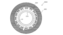
- the ⁇ LED ultraviolet radiation source 2000 includes a member 600 having a curved surface or a corner portion, and the flexible film 520 is attached to the member 600.
- This member 600 has a semimajor portion having an inner surface and an outer surface in the example of FIG.
- the member 60 has a cylindrical shape extending in a direction perpendicular to the paper surface in the drawing.
- the flexible film 520 equipped with a plurality of individualized ⁇ LED 220s is attached to the inner surface of such a long axis portion.
- Each of the plurality of light emitting element units 10 may include a plurality of ⁇ LEDs 220 arranged in a predetermined direction.
- a material to be irradiated with ultraviolet rays for example, a fluid such as water containing an object to be sterilized, flows inside a pipe 620 located at a central portion.
- the pipe 620 is made of a material that transmits ultraviolet rays well, such as quartz.
- the plurality of light emitting element units 10 arranged so as to surround the circumference of the pipe 620 each have one or a plurality of ⁇ LEDs 220 that emit ultraviolet rays. Further, it is preferable that at least the inner wall surface of the member 600 surrounding the light emitting element unit 10 is made of a material or a film that reflects ultraviolet rays.
- the ultraviolet rays radiated from a large number of ⁇ LED 220s efficiently collect inside the pipe 620, so that the irradiation intensity required for processing such as sterilization can be achieved in a short time.
- a film formed of a material having a photocatalytic effect is deposited on the inner wall of the pipe 620, it is possible to prevent the adhesion of dirt.
- a typical example of such a film is a TiO 2 film.
- the thickness of the film is preferably such that it does not interfere with the transmission of ultraviolet rays (for example, 5 to 20 nm).
- the irradiation intensity and irradiation time of ultraviolet rays can be set in units of light emitting element units or in units of ⁇ LED.
- a simple electric circuit for connecting each light emitting element unit or each ⁇ LED unit to a common power supply line may be provided in the backplane 400.
- an electric circuit including a TFT for driving an active matrix may be provided on the backplane 400.
- the form of the ⁇ LED ultraviolet radiation source 2000 is not limited to an example having a configuration in which ultraviolet rays are emitted in a closed space as shown in FIG.
- the flexible film 520 in which a plurality of light emitting element units 10 are arranged is attached to the surface of an object having a complicated outer shape, and can also radiate ultraviolet rays outward.
- the effect that the directivity of ultraviolet radiation can be freely controlled can be obtained. Even if the same effect is obtained by the conventional pickup-and-place method, it is practically impossible to mount a large number of ⁇ LEDs on a non-planar surface while adjusting the orientation.
- a structure similar to the ⁇ LED ultraviolet radiation source 1000 shown in FIGS. 1A and 1B is produced by the method described above.
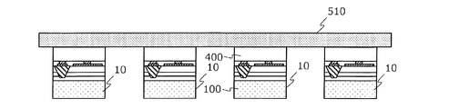
- a step of dividing the crystal growth substrate 100 and the laminated structure on the crystal growth substrate 100 into a plurality of light emitting element units 10 is performed. Specifically, for example, as shown in FIG. 17A, after the backplane 400 is fixed on the expansion film 510, the boundary positions of the plurality of light emitting element units 10 are cut by a laser beam or a dicing blade. In this way, a cutting groove is formed between the adjacent light emitting element units 10.
- the distance between the centers of the plurality of light emitting element units 10 is increased as shown in FIG. 17B.
- the distance between the centers before expansion can be expanded to, for example, 1.2 to 2.5 times or more (about 5 times) after expansion.
- a plurality of light emitting element units 10 are simultaneously or sequentially moved (transferred) to the flexible film 520 as shown in FIG. 17B. After transfer, the expansion film 510 can be peeled off.
- the flexible film 520 can be flexibly deformed according to the surface shape of the object to be fixed.
- electrode pads and wiring for electrically connecting to the backplane 400 are provided on the surface of the flexible film 520 facing the backplane 400.
- the wiring may have materials and structures that can be extended with the flexible film 520.
- An example of such a material is a resin in which conductive particles are dispersed, or a conductive polymer (conductive polymer) which itself has conductivity.
- An example of such a structure is a meandering or bent wiring pattern, which has a shape that does not break even when the flexible film 520 expands.
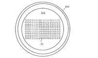
- the expansion device 800 shown in FIG. 19A can be used.
- the expansion device 800 grips the circumferential portion of the circular expansion film 510, and the upper surface of the columnar movable stage (not shown) is in contact with the back surface of the expansion film 510.
- the expansion device 800 pushes the movable stage toward the front of the drawing while heating the expansion film 510 on the upper surface of the movable stage while maintaining the circumferential portion of the expansion film 510 in a predetermined position.
- the expansion film 510 can be expanded from the center to the outside in the radial direction.
- FIG. 19B shows a state in which the expansion device 800 moves the movable stage toward the front side of the drawing and expands the expansion film 510 from the center to the outside in the radial direction.
- the plurality of light emitting element units 10 supported by the expansion film 510 each shift their positions to increase the distance between them. For example, after fixing the flexible film 520 shown in FIG. 17B to the expansion film 510 in such a state, the expansion film 510 may be removed from the expansion device 800.
- each light emitting element unit 10 is cut and separated so as to have a size smaller than, for example, 1000 ⁇ m ⁇ 1000 m (for example, 100 ⁇ m ⁇ 100 m) and separated into individual pieces.
- the form is not limited to such an example.
- Each light emitting element unit 10 may have a striped shape extending in a predetermined direction. For example, when the flexible film 520 is deformed along the cylindrical surface as shown in FIG. 16, the fact that the light emitting element unit 10 extends in the long axis direction does not hinder the deformation.
- the expansion film 510 does not function as a component of the final ⁇ LED ultraviolet radiation source 2000, but the embodiments of the present disclosure are not limited to such examples.
- FIG. 18A in a state where the backplane 400 of the divided plurality of light emitting element units 10 is fixed to the expansion film 510, the distance between the centers of the plurality of light emitting element units 10 is widened, and the state shown in FIG. 18B. It may be transformed into.
- the adhesive layer provided on the expansion film 510 may be formed from an adhesive whose adhesive strength is not reduced by ultraviolet irradiation. preferable.
- a functional layer such as a wiring layer or a printed circuit board may be attached to the back surface of the flexible film 520 of FIG. 17B or the back surface of the expansion film 510 of FIG. 18B.
- the cutting for division is executed from the backplane 400 side, whereas in the example shown in FIG. 18A, such cutting is executed from the substrate 100 side. become.
- another film such as a dicing film is attached to the substrate 100 or the backplane 400 at the time of cutting, and the dicing film is expanded after cutting. It may be transferred to the film 510.
- Each light emitting device unit 10 may include one or more ⁇ LED 220s.
- the ⁇ LED ultraviolet radiation source 2000 shown in FIG. 16 includes a flexible film 520 fixed to the inner wall surface of the cylindrical member 600, but the flexible film 520 is fixed to the outer wall surface of the cylindrical member 600. It may be used by being fixed to any other member having various shapes.
- Embodiments of the present invention provide a new micro LED ultraviolet radiation source.
- the micro LED ultraviolet radiation source can be used in various applications requiring irradiation with ultraviolet rays, such as ultraviolet curing of a resin, exposure of a resist, lift-off of a resin film, and sterilization. In particular, it is useful in an apparatus that requires selective irradiation of a predetermined area with ultraviolet rays.
Landscapes
- Led Devices (AREA)
Abstract
本開示のマイクロLED紫外放射源は、結晶成長基板(100)と、それぞれが第1導電型の第1半導体層(21)および第2導電型の第2半導体層(22)を有する複数のマイクロLED(220)、ならびにマイクロLEDの間に位置する素子分離領域(240)を含むフロントプレーン(200)とを備える。素子分離領域は、第2半導体層に電気的に接続された少なくともひとつの金属プラグ(24)を有する。このμLED紫外放射源は、第1半導体層に電気的に接続された第1コンタクト電極(31)および金属プラグに接続された第2コンタクト電極(32)を含む中間層(300)と、中間層上に形成されたバックプレーン(400)とを備える。基板、フロントプレーン、中間層、バックプレーンは、複数の発光素子ユニットに分割されており、複数の発光素子ユニットは可撓性フィルムに支持されている。
Description
本開示は、マイクロLED紫外放射源及びその製造方法に関する。
紫外線を放射する光源として、蛍光ランプおよび水銀ランプの代わりに、深紫外LED(Light Emitting Diode)を用いる装置が提案されている。
特許文献1は、深紫外LED群を金属製放熱基板上に並べて配置し、その外側を石英ガラスパッケージで覆った殺菌装置を開示している。
多数の深紫外LEDを例えば湾曲した部材上に実装することは困難である。
本開示は、上記の課題を解決することができる、新規な紫外放射源を提供する。
本開示のマイクロLED紫外放射源は、例示的な実施形態において、結晶成長基板と、前記結晶成長基板上のフロントプレーンであって、それぞれが第1導電型の第1半導体層および第2導電型の第2半導体層を有して紫外線を放射する複数のマイクロLED、ならびに前記複数のマイクロLEDの間に位置する素子分離領域を含み、前記素子分離領域が、前記第2半導体層に電気的に接続された少なくともひとつの金属プラグを有している、フロントプレーンと、前記フロントプレーンに支持された中間層であって、それぞれが前記複数のマイクロLEDの前記第1半導体層に電気的に接続された複数の第1コンタクト電極、および前記金属プラグに接続された少なくともひとつの第2コンタクト電極を含む、中間層と、前記中間層に支持されたバックプレーンであって、前記複数の第1コンタクト電極および前記少なくともひとつの第2コンタクト電極を介して前記複数のマイクロLEDに電気的に接続された電気回路を有する、バックプレーンとを備える。前記結晶成長基板、前記フロントプレーン、前記中間層、および前記バックプレーンは、複数の発光素子ユニットに分割されている。前記複数の発光素子ユニットのそれぞれは、前記複数のマイクロLEDの少なくともひとつを含み、前記複数のマイクロLEDから放射された前記紫外線は、前記結晶成長基板を透過して外部に出射され、前記複数の発光素子ユニットは可撓性フィルムに支持されている。
ある実施形態において、前記バックプレーンは、前記中間層上に成長した金属、半導体、および/または絶縁材料の層を含んでいる。
ある実施形態において、前記素子分離領域は、前記複数のマイクロLEDのそれぞれから放射された紫外線を前記結晶成長基板に向けて反射するリフレクタを備えている。
ある実施形態において、前記リフレクタの少なくとも反射面は、アルミニウム(Al)またはロジウム(Rh)から形成されている。
ある実施形態において、前記紫外線の波長は、200nm以上380nm以下である。
ある実施形態において、前記少なくともひとつの金属プラグの少なくとも一部が前記リフレクタとして機能する。
ある実施形態において、前記複数のマイクロLEDのそれぞれは、順テーパの側面を有しており、前記少なくともひとつの金属プラグは、前記複数のマイクロLEDのそれぞれが有する前記側面に接触している。
ある実施形態において、前記結晶成長基板はサファイア基板である。
ある実施形態において、曲面または角部を有する部材を更に備え、前記可撓性フィルムは、前記曲面または前記角部に付着している。
ある実施形態において、前記部材は、内面および外面を有する長軸部分を有しており、前記長軸部分は、所定方向に延びており、前記可撓性フィルムは、前記長軸部分の前記内面および/または前記外面に付着している。
ある実施形態において、前記複数の発光素子ユニットのそれぞれは、前記所定方向に配列された複数の前記マイクロLEDを含む。
ある実施形態において、前記電気回路は、薄膜トランジスタを含む。
ある実施形態において、前記複数の発光素子ユニットのそれぞれにおいて、前記フロントプレーンの前記素子分離領域は、前記複数のマイクロLEDの側面を覆う絶縁物を有しており、前記絶縁物は、前記金属プラグのための少なくともひとつのスルーホールを有している。
ある実施形態において、前記可撓性フィルムは、前記複数の発光素子ユニットの前記バックプレーンを電気的に接続する配線層を有している。
本開示のマイクロLED紫外放射源の製造方法は、例示的な実施形態において、結晶成長基板と、前記結晶成長基板に支持されたフロントプレーンであって、それぞれが第1導電型の第1半導体層および第2導電型の第2半導体層を有して紫外線を放射する複数のマイクロLED、ならびに前記複数のマイクロLEDの間に位置する素子分離領域を含み、前記素子分離領域が、前記第2半導体層に電気的に接続された少なくともひとつの金属プラグを有している、フロントプレーン、および前記フロントプレーンに支持された中間層であって、それぞれが前記複数のマイクロLEDの前記第1半導体層に電気的に接続された複数の第1コンタクト電極、および前記金属プラグに接続された少なくともひとつの第2コンタクト電極を含む、中間層を備える積層構造体を用意する工程と、前記積層構造体上にバックプレーンを形成する工程であって、前記複数の第1コンタクト電極および前記少なくともひとつの第2コンタクト電極を介して前記複数のマイクロLEDに電気的に接続された電気回路を有する、バックプレーンを形成する工程と、前記積層構造体および前記バックプレーンを複数の発光素子ユニットに分割する工程と、前記複数の発光素子ユニットを可撓性フィルムに転写する工程と、を含む。
ある実施形態において、前記複数の発光素子ユニットを前記可撓性フィルムに転写する工程は、前記結晶成長基板に拡張フィルムを付着し、前記拡張フィルムを拡張することにより、前記複数の発光素子ユニットの間隔を広くする工程と、拡張した前記拡張フィルム上の前記複数の発光素子ユニットを前記可撓性フィルムに付着させる工程と、を含む。
ある実施形態において、前記複数の発光素子ユニットを前記可撓性フィルムに転写する工程は、前記バックプレーンに拡張フィルムを付着し、前記拡張フィルムを拡張することにより、前記複数の発光素子ユニットの間隔を広くする工程と、拡張した前記拡張フィルムを、前記複数の発光素子ユニットが付着したままで、曲面または角部を有する部材にさらに付着させる。
本発明の実施形態によれば、前記の課題を解決するマイクロLED紫外放射源が提供される。
<定義>
本開示における「マイクロLED」とは、占有領域のサイズが、1000μm×1000μmの領域内、または、幅が1000μm以下のストライプ状領域内に含まれる大きさを有する発光ダイオード(LED)を意味する。本開示におけるマイクロLEDが放射する電磁波は、波長380nm以下の紫外線である。以下、「マイクロLED」を「μLED」と表記することがある。
本開示における「マイクロLED」とは、占有領域のサイズが、1000μm×1000μmの領域内、または、幅が1000μm以下のストライプ状領域内に含まれる大きさを有する発光ダイオード(LED)を意味する。本開示におけるマイクロLEDが放射する電磁波は、波長380nm以下の紫外線である。以下、「マイクロLED」を「μLED」と表記することがある。
μLEDは、第1導電型の第1半導体層および第2導電型の第2半導体層を有する。第1導電型はp型およびn型の一方であり、第2導電型はp型およびn型の他方である。例えば第1導電型がp型であるとき、第2導電型はn型である。逆に第1導電型がn型であるとき、第2導電型はp型である。第1半導体層および第2半導体層のそれぞれは、単層構造または多層構造を有し得る。典型的には、少なくとも1個の量子井戸(またはダブルヘテロ構造)を有する発光層が第1半導体層と第2半導体層との間に形成される。
本開示における「マイクロLED紫外放射源(μLED-UV源)」とは、それぞれが紫外線を放射する複数のμLEDを備えるデバイスである。μLED-UV源における複数のμLEDを「μLEDアレイ」と呼ぶことがある。μLED-UV源は、樹脂の紫外線硬化、レジストの感光、殺菌など、紫外線の照射が求められる各種の用途に利用され得る。特に、本開示のμLED-UV源は、マスクレスで任意の照射パターンを実現できる。
<基本構成>
図1Aおよび図1Bを参照して、本開示のμLED-UV源の基本構成例を説明する。図1Aは、μLED-UV源1000の一部を示す断面図である。図1Bは、μLED-UV源1000におけるμLEDアレイの配置例を示す平面図である。図1Aに示されているμLED-UV源1000の断面は、図1BのA-A線断面に相当する。
図1Aおよび図1Bを参照して、本開示のμLED-UV源の基本構成例を説明する。図1Aは、μLED-UV源1000の一部を示す断面図である。図1Bは、μLED-UV源1000におけるμLEDアレイの配置例を示す平面図である。図1Aに示されているμLED-UV源1000の断面は、図1BのA-A線断面に相当する。
μLED-UV源1000は、例えば数百~数千個、または1万個を超えるような多数のμLEDを備え得る。図1Aおよび図1Bは、μLED-UV源1000のうちの、数個のμLEDを含む一部分のみを示している。μLED-UV源1000の全体は、図示されている部分が、例えば周期的に、または、特定のパターンで配列された構成を備えている。
μLED-UV源1000では、従来の大きな1個のLED素子に含まれる一層の連続した発光層から紫外線を放射させるのではなく、小さく分割された複数のμLEDから紫外線を放射させる。このため、個々のμLEDに含まれる発光層の端面からの紫外線放射をどのように利用するかが重要になる。μLEDのサイズが縮小し、かつ、μLED-UV源1000に含まれるμLEDの個数が増加するにつれて、発光層における半導体層の積層方向に垂直な面積に対する端面の面積の比率が増加するからである。本開示の実施形態では、後述するリフレクタを個々のμLEDの間の領域(素子分離領域)に設けることにより、発光層から横方向に放射された紫外線をも有効に活用することが可能になる。
μLED-UV源1000は、結晶成長基板100と、結晶成長基板100に支持されたフロントプレーン200と、フロントプレーン200に支持された中間層300と、中間層に支持されたバックプレーン400とを備えている。
添付図面において、μLEDなどの各構成要素の縦方向サイズに対する横方向サイズの比率は、実施形態における実際の比率を必ずしも反映していない。図面では、わかりやすさを優先した比率で各構成要素が記載されている。また図面における各構成要素の向きは、実際にμLED-UV源を製造するときの向き、および、使用時における向きを何ら制限しない。図1Aおよび図1Bには、参考のため、相互に直交するX軸、Y軸、およびZ軸の座標軸が記載されている。
<結晶成長基板>
結晶成長基板100は、μLEDを構成する半導体結晶がエピタキシャル成長する基板である。本開示において、結晶成長基板100はサファイア基板である。以下、サファイアから形成された結晶成長基板100を単に「基板(substrate)」と称する。基板100の結晶成長が生じる面100Tを「上面」または「結晶成長面」と呼び、基板100の反対側の面100Bを「下面」と称する。本明細書において、「上面」および「下面」の語句は、基板100の実際の向きに依存することなく用いられる。
結晶成長基板100は、μLEDを構成する半導体結晶がエピタキシャル成長する基板である。本開示において、結晶成長基板100はサファイア基板である。以下、サファイアから形成された結晶成長基板100を単に「基板(substrate)」と称する。基板100の結晶成長が生じる面100Tを「上面」または「結晶成長面」と呼び、基板100の反対側の面100Bを「下面」と称する。本明細書において、「上面」および「下面」の語句は、基板100の実際の向きに依存することなく用いられる。
本開示の実施形態で利用され得る半導体結晶の典型例は、窒化ガリウム系化合物半導体である。以下、窒化ガリウム系化合物半導体を「GaN」と表記することがある。GaNにおけるガリウム(Ga)原子の一部は、アルミニウム(Al)原子またはインジウム(In)原子によって置換されていてもよい。Ga原子の一部がAl原子で置換されたGaNを「AlGaN」と表記する場合がある。また、Ga原子の一部がIn原子で置換されたGaNを「InGaN」と表記する場合がある。更には、Ga原子の一部がAl原子およびIn原子で置換されたGaNを「AlInGaN」または「InAlGaN」と表記することがある。GaNのバンドギャップは、AlGaNのバンドギャップよりも小さく、InGaNのバンドギャップよりも大きい。なお、本開示では、構成原子の一部が他の原子で置換された窒化ガリウム系化合物半導体を総称して「GaN」と表記する場合がある。「GaN」には、不純物イオンとしてn型不純物および/またはp型不純物がドープされ得る。導電型がn型であるGaNは「n-GaN」、導電型がp型であるGaNは「p-GaN」と表記する。半導体結晶の成長方法の詳細については、後述する。なお、本開示の実施形態において、μLEDを構成する半導体結晶は、GaN系半導体に限定されず、AlN、InN、またはAlInNなどの窒化物半導体、あるいは他の半導体から形成されていてもよい。
本開示の実施形態において、基板100は、最終的なμLED-UV源1000の構成要素である。基板100の厚さは、例えば30μm以上1000μm以下、好ましくは500μm以下であり得る。基板100の役割は、結晶成長のベースとなること、および、動作時における紫外線取り出し効率を向上させるための光学部材である。このため、μLED-UV源1000の剛性は、基板100以外の他の剛性部材によって補われてもよい。そのような剛性部材は、例えばバックプレーン400に固着され得る。なお、製造工程中においては、基板100の下面100Bに基板100の剛性を補う支持基板(不図示)を固定してもよい。このような支持基板は、最終的なμLED-UV源1000からは除去され得る。
基板100の上面(結晶成長面)100Tには、結晶格子歪を緩和するような溝またはリッジなどの構造が付与されていてもよい。また、結晶格子歪を低減するためのバッファ層が基板100の上面100Tに形成されていてもよい。基板100の下面100Bには、μLEDアレイから放射され、基板100を透過してきた紫外線の取り出し効率を更に向上させたり、紫外線を拡散させたりするための微細な凹凸が形成されていてもよい。微細な凹凸の例はモスアイ構造を含む。モスアイ構造は、基板100の下面100Bにおける実効的な屈折率を連続的に変化させるため、基板100の下面100Bで基板100の内側に反射される割合(反射率)を大きく低下させる(実質的にゼロにする)ことができる。
本開示において、図1Aに示されるZ軸の正方向(矢印の向き)を「結晶成長方向」または「半導体積層方向」と呼ぶ場合がある。また、基板100の下面100Bおよび上面100Tを、それぞれ、基板100の「正面」および「背面」と呼んでもよい。
<フロントプレーン>
フロントプレーン200は、複数のμLED220と、複数のμLED220の間に位置する素子分離領域240とを含む。複数のμLED220は、基板100の上面100Tに平行な2次元平面(XY面)内において、行および列状に配列され得る。複数のμLED220のそれぞれは、図1Aに示されるように、第1導電型の第1半導体層21および第2導電型の第2半導体層22を有する。第2半導体層22は、第1半導体層21に比べて、基板100に近い位置にある。
フロントプレーン200は、複数のμLED220と、複数のμLED220の間に位置する素子分離領域240とを含む。複数のμLED220は、基板100の上面100Tに平行な2次元平面(XY面)内において、行および列状に配列され得る。複数のμLED220のそれぞれは、図1Aに示されるように、第1導電型の第1半導体層21および第2導電型の第2半導体層22を有する。第2半導体層22は、第1半導体層21に比べて、基板100に近い位置にある。
本開示の実施形態において、各μLED220は、他のμLED220から独立して発光し得る発光層23を有している。発光層23は、第1半導体層21と第2半導体層22との間に位置している。素子分離領域240は、第2半導体層22に電気的に接続された少なくともひとつの金属プラグ24を有している。金属プラグ24は、μLED220の基板側電極として機能する。
第1導電型の第1半導体層21の典型例は、p-GaN層である。第2導電型の第2半導体層22の典型例は、n-GaN層である。p-GaN層およびn-GaN層は、それぞれ、基板100の上面100Tに垂直な方向(半導体積層方向:Z軸の正方向)に沿って同一の組成を有している必要はなく、多層構造を有し得る。前述したように、GaNのGaはAlおよび/またはInによって少なくとも部分的に置換され得る。このような置換は、GaNのバンドギャップおよび/または屈折率を調整するために行われ得る。また、n型不純物およびp型不純物の濃度、すなわちドーピングレベルも、半導体積層方向(Z軸の正方向)に沿って一様である必要はない。
発光層23の典型例は、紫外線を発するため、少なくともひとつのAlGaNまたはInAlGaN井戸層を含む。発光層23が複数の井戸層を含む場合、それぞれの井戸層の間には、井戸層よりもバンドギャップが大きな障壁層が配置され得る。井戸層のバンドギャップは、発光波長を規定する。具体的には、真空中における発光波長をλ[nm]、バンドギャップをEg[エレクトロンボルト:eV]とすると、λ×Eg=1240の関係が成立する。従って、例えばλ=350nmの紫外線を放射させるには、井戸層のバンドギャップEgを約3.54eVに調整すればよい。例えばAlGaN井戸層のバンドギャップは、AlGaN井戸層におけるAl組成比率に応じて調整され得る。
各μLED220を構成する上記複数の半導体層は、それぞれ、基板100上にエピタキシャル成長した単結晶の層(エピタキシャル層)である。素子分離領域240は、基板100上にエピタキシャル成長した複数の半導体層を部分的にエッチングすることによって形成されたトレンチ状の凹部(以下、「トレンチ」と称する)によって規定される。トレンチによって分離された個々のμLED220の占有領域は、1000μm×1000μmの領域内に含まれる大きさ(例えば100μm×100μmの領域またはそれ以下)を有している。なお、μLED220の占有領域は、素子分離領域240によって区分された第1半導体層21および/または発光層23の輪郭によって規定される。
図1Bに示されるように、素子分離領域240は各μLED220を取り囲み、個々のμLED220を他のμLED220から分離している。より具体的には、素子分離領域240は、個々のμLED220の第1半導体層21および発光層23を、他のμLED220の第1半導体層21および発光層23から、電気的・空間的に分離している。
図1Aに示されるように、第2半導体層22は、μLED220ごとに完全に分離されていなくてもよい。図1Aに示される例において、複数のμLED220のそれぞれが有する第2半導体層22は、1層の連続した半導体層から形成されており、複数のμLED220によって共有されている。1層の連続した第2半導体層22が複数のμLED220によって共有されていると、この第2半導体層22が複数のμLED220に対する第2導電側の共通電極として機能する。もし、各μLED220の第2半導体層22が相互に分離され、かつ、第2半導体層22が個別にバックプレーン400における第2導電側の電極(配線)に接続されている形態では、第2導電側の電極または配線の一部に断線不良が発生すると、一部のμLED220に通電不良が発生してしまう。しかし、複数のμLED220のそれぞれが有する第2半導体層22が1層の連続した半導体層から形成されている形態によれば、そのような不良の発生を抑制することができる。本開示の実施形態は、このような例に限定されない。各μLED220の第2半導体層22は、金属プラグ24、または後述するTiNバッファ層などと適切に接続されているのであれば、他のμLED220の第2半導体層22から分離されていてもよい。
この例において、素子分離領域240は、複数のμLED220の間を埋める(fill)埋め込み絶縁物(embedded insulator)25を有している。埋め込み絶縁物25は、金属プラグ24のための1個または複数個のスルーホールを有している。スルーホールは金属プラグ24を構成する金属材料によって埋められている。金属プラグ24は、異なる金属の層がスタックされた構造を有していてもよい。
本開示の実施形態において、フロントプレーン200の上面は、図1Aに示されるように平坦化されていることが好ましい。このような平坦化は、素子分離領域240における金属プラグ24および埋め込み絶縁物25の上面のレベルが、μLED220における第1半導体層21の上面のレベルに略一致することにより実現されている。
<リフレクタ>
本開示の実施形態において、μLED-UV源1000の素子分離領域240は、複数のμLED220のそれぞれから放射された紫外線を結晶成長基板100に向けて反射するリフレクタ260を備えている。より具体的には、素子分離領域240は、複数のμLED220の間を埋める埋め込み絶縁物25を有しており、埋め込み絶縁物25は、金属プラグ24のためのV字型溝(スルーホール)を有している。埋め込み絶縁物25は、μLED220から放射された紫外線を透過する材料から形成される。
本開示の実施形態において、μLED-UV源1000の素子分離領域240は、複数のμLED220のそれぞれから放射された紫外線を結晶成長基板100に向けて反射するリフレクタ260を備えている。より具体的には、素子分離領域240は、複数のμLED220の間を埋める埋め込み絶縁物25を有しており、埋め込み絶縁物25は、金属プラグ24のためのV字型溝(スルーホール)を有している。埋め込み絶縁物25は、μLED220から放射された紫外線を透過する材料から形成される。
金属プラグ24は、V字型溝の底で第2半導体層22に接触している。この金属プラグ24は、各μLED220をバックプレーン400に電気的に接続するための導電体として機能するだけではなく、リフレクタ260としても機能する。図示されているように、金属プラグ24の側面(反射面260S)は、結晶成長基板100の上面100Tに対して直交しておらず、傾斜している。金属プラグ24は、少なくとも第2半導体層22に接触する部分においてオーミックコンタクトを実現する材料から形成されていることが望ましい。しかし、他の部分は、種々の金属材料から形成され得る。例えば、Al、Ag、Rh、Au、Cu、Pd、Pt、Ti、Ni、Mo、およびWからなる群から選択された少なくとも1種の金属から形成され得る。本発明者の検討によれば、μLED220から放射される紫外線を高い反射率(例えば90%以上)で反射するという観点からは、金属プラグ24の少なくとも側面(リフレクタ260の反射面260S)は、Alから形成されていることが望ましい。実用的な反射率として70%以上を確保しようとする場合、リフレクタ260の反射面260Sは、Al、AgまたはRhから形成されていることが好ましい。特に波長300nm以下の紫外線に対するリフレクタ260の反射面260Sとしては、AlまたはRhが望ましい。後述するシミュレーションの結果、例えば、波長350nmの紫外線の反射率は、Al>Ag>Rh≫Cu≒Tiの関係を有していることがわかった。また、波長300nm以下の紫外線の反射率は、Al>Rh≫Ti>Cu>Agの関係を有する。
リフレクタ260として機能する金属プラグ24は、図1Bに示されるように、個々のμLED220を取り囲んでいる。このため、μLED220から四方に放射された紫外線は、金属プラグ24の傾斜した側面(反射面260S)によって結晶成長基板100の方向に反射される。金属プラグ24は、格子形状を有する1個の導電物である必要はなく、複数の部分に分離されていてもよい。
<リフレクタの他の形態>
次に、図2を参照する。図2に示される例では、金属プラグ24が側面に反射層28を有しており、この反射層28がリフレクタ260として機能する。反射層28は、金属プラグ24の材料とは異なる材料、例えばAlあるいはRhから形成され得る。反射層28の厚さは、例えば30nm以上50nm以下である。反射層28は、金属以外の材料から形成されていてもよい。反射層28は、例えば、埋め込み絶縁物25の屈折率とは異なる屈折率を有する誘電体材料から形成され得る。反射層28と埋め込み絶縁物25との界面に存在する屈折率差を利用してμLED220から放射された紫外線を反射することができる。この界面を透過して金属プラグ24に入射した紫外線は、金属プラグ24そのものによって反射され得る。
次に、図2を参照する。図2に示される例では、金属プラグ24が側面に反射層28を有しており、この反射層28がリフレクタ260として機能する。反射層28は、金属プラグ24の材料とは異なる材料、例えばAlあるいはRhから形成され得る。反射層28の厚さは、例えば30nm以上50nm以下である。反射層28は、金属以外の材料から形成されていてもよい。反射層28は、例えば、埋め込み絶縁物25の屈折率とは異なる屈折率を有する誘電体材料から形成され得る。反射層28と埋め込み絶縁物25との界面に存在する屈折率差を利用してμLED220から放射された紫外線を反射することができる。この界面を透過して金属プラグ24に入射した紫外線は、金属プラグ24そのものによって反射され得る。
図3は、μLED-UV源1000の他の構成例を示す断面図である。この例における複数のμLED220のそれぞれは、傾斜した側面220Sを有している。金属プラグ24は、各μLED220が有する側面220Sに接触している。この例において、金属プラグ24は、各μLED220が有する側面220Sに接触する反射面260Sを有しており、リフレクタ260として機能する。この例において、反射面260Sの傾斜角度θは、各μLED220が有する側面220Sの傾斜角度を規定する。図3に示される例において、反射面260Sの傾斜角度θは90度未満(例えば30~60度)である。μLED220が有する側面220Sは順テーパを形成している。
金属プラグ24の表面は、第2半導体層22に対してオーミック接触を実現できる材料から形成されることが好ましい。第2半導体層22がn-GaNから形成されている場合、n-GaNの仕事関数Φnよりも小さな仕事関数Φmを有する金属(例えばTi)を用いることにより、第2半導体層22と金属プラグ24との間に選択的なオーミック接触を実現する一方で、p-GaNから形成された第1半導体層21と金属プラグ24との間に高抵抗層を形成することができる。図3の構成例によれば、素子分離領域240に埋め込み絶縁物25を形成する工程および埋め込み絶縁物25にスルーホールを形成する工程を省略できる。
図3の構成例では、金属プラグ24の構成は、上記の例に限定されず、積層構造(上層金属および下層金属)を有していてもよい。上層金属と第1半導体層21との間には高抵抗または絶縁性の界面が形成されるように上層金属の材料が選択されるとともに、下層金属と第2半導体層22との間には低抵抗オーミック接触が形成されるように下層金属の材料が選択される。このとき、以下に説明するように、紫外線に対する反射率の高い材料が少なくとも発光層23に接することが好ましい。
なお、第1半導体層21がp-GaNから形成されている場合、オーミック接触の形成は一般に困難であり、また、素子分離のためエッチングによる損傷がp-GaNと金属プラグ24との間の抵抗を形成する。このため、図3に示されるように、第1半導体層21と第2半導体層22との間が金属プラグ24によって電気的にショートする問題は回避される。
<リフレクタの傾斜角度および材料>
図4Aおよび図4Bは、発光層23で発生した紫外線が金属プラグ24によって反射される様子を模式的に示している。図示される例において、金属プラグ24のうち、紫外線を反射する領域には高反射率層24Rが設けられている。高反射率層24Rがリフレクタ260として機能する。μLED内の発光層23で発生した紫外線は、基本的には、等方的に放射されるが、相対的にバンドギャップが大きく、屈折率の高い発光層23に沿って横方向に導波されやすい。このため、高い反射率を実現し、かつ、適切な角度で紫外線を基板100に入射させるには、発光層23に対するリフレクタ260の傾斜角度が重要になる。
図4Aおよび図4Bは、発光層23で発生した紫外線が金属プラグ24によって反射される様子を模式的に示している。図示される例において、金属プラグ24のうち、紫外線を反射する領域には高反射率層24Rが設けられている。高反射率層24Rがリフレクタ260として機能する。μLED内の発光層23で発生した紫外線は、基本的には、等方的に放射されるが、相対的にバンドギャップが大きく、屈折率の高い発光層23に沿って横方向に導波されやすい。このため、高い反射率を実現し、かつ、適切な角度で紫外線を基板100に入射させるには、発光層23に対するリフレクタ260の傾斜角度が重要になる。
図4Aおよび図4Bに示されているリフレクタ260の反射面260Sは、発光層23から受けた紫外線を下方(Z軸の負方向)に反射する。
本開示では、リフレクタ260の反射面260SとXY面との間の角度を「反射面の傾斜角度θ」と定義する。また、反射面260Sの法線Nに対して、発光層23を伝搬してきた紫外線がなす角度をαとする。このとき、θ+α=90度の関係が成立する。反射面260Sで反射された紫外線は、Z軸負方向に対して|2θ-90|度の角度をなす方向に進む。Z軸負方向に対する|2θ-90|度で表される角度を「基板入射角」と称することにする。
図4Bに示されている例において、半導体層21、22、23の側面(μLED220の側面220S)は傾斜角度θで傾斜し、順テーパを形成している。図4Bに示されている構成例について、本発明者がシミュレーションを行ったところ、紫外線の光取り出しを実現するためには、基板入射角が25度以下であることが必要であり、好ましくは15度以下、より好ましくは10度以下であることがわかった。従って、リフレクタ260の反射面260Sの傾斜角であるθは、32.5~57.5度の範囲にあることが必要であり、角度θは、好ましくは37.5~52.5度、より好ましくは40~50度の範囲にある。
角度θが40~50度の範囲にあるとき、90%程度の高い光取り出し効率が実現する。しかし、このような高い光取り出し効率は、基板100がサファイアから形成されている場合に達成され、他の材料、例えばGaNから形成されている場合には達成されない。具体的には、基板100がGaN基板の場合、波長375nm以下の紫外線は、基板入射角が0度であっても取り出すことはできない。
後述するように、基板100の上面100Tには窒化チタニウム(TiN)層が形成されてもよい。TiN層は結晶成長に寄与するが、紫外線の透過に影響を与える。本発明者の検討によると、基板入射角を23度以下にすれば、紫外線の取り出しが可能になる。厚さが5~15nmのTiN層が存在する場合、基板入射角は10度以下であることが好ましい。基板入射角が10度以下であれば、60%以上の光取り出し効率が実現し得る。
金属プラグ24(リフレクタ260)の反射面260Sにおける材料は、紫外線に対して反射率が高いAlまたはRhであることが好ましい。反射面260SがAl層またはRh層によって形成されていれば、金属プラグ24(リフレクタ260)の内部は他の金属、例えばCu、Ag、Ti、TiNなどから形成されていてもよい。Al層またはRh層が50nm程度までは厚くなるほど、紫外線反射率は増加する傾向があることもわかった。リフレクタとして機能するAl層またはRh層の好ましい厚さは、例えば30nm以上である。
発明者のシミュレーションによると、可視光の波長範囲では比較的高い反射率を示す金属であっても、例えば殺菌に利用される波長200nm以上300nm以下の範囲においては、AlおよびRh以外の金属で、反射率が著しく低下することがわかった。例えば、図4Bの例において角度θ=45°、リフレクタ260の反射面260Sを構成する金属膜の層厚が30nmのとき、図4Cに示すように、Alの反射率は波長200~380nmの広い範囲で、ほぼ90%以上である。Rhの反射率も、波長200~380nmの広い範囲で、ほぼ68%以上である。これに対して、例えばAgの反射率は、図4Dに示すように、波長350nmで85%程度であるが、波長295nmで37%に減少する。またCuの反射率は、波長380nmで50%以上、波長260~280nm付近で約40%である。CuとAgとを詳細に比較すると、波長200nm~280nmの範囲の反射率は、Cu≒Agであるのに対して、280nm~305nmの範囲ではCu>Agであり、305nmを超えるとAg≫Cuとなる。このため、波長が305nmより大きい領域ではAgが好ましく、波長が300nm近傍ではCuが好ましい。なお、Alは、これらの波長範囲の全体でAg、Cuよりも高い反射率を示す。Rhは、318nm以上ではAgよりも低いが、それ以外の特に300nm以下では、Ag、Cuよりも高い反射率を示す。
以上のことから明らかなように、本開示のμLED紫外放射光源を殺菌用途(波長:200nm以上300nm以下、典型的には250nm以上300nm以下)に利用する場合、リフレクタ260の少なくとも反射面260Sは、AlまたはRhから形成されることが望ましい。
紫外線の領域で高い反射率を達成するため、反射面260Sを構成するAlまたはRhの層厚は、30nm程度以上であることが望ましい。この層厚を50nm以上に増加させても、反射率の増加は飽和する。したがって、リフレクタ260として機能する部分におけるAlまたはRの層厚は30~50nmであることが好ましい。金属プラグ24のうち、側面から厚さ30~50nm程度の表層領域を除く他の部分は、紫外線反射率を考慮することなく、電気抵抗率またはコンタクト抵抗を低減する観点から、他の金属を選択することができる。
半導体層に対するオーミックコンタクト性を高める観点から、TiNを金属プラグ24のコンタクト部分に用いることが好ましいが、反射面260SにTiN層が存在すると、紫外線に対する反射率は低下する。反射面260SにTiN層などのAl層以外の金属層が存在する場合、角θを40度以下にすることが好ましい。各θが小さいほど、反射率が向上する。
金属プラグ24(リフレクタ260)のX軸方向(またはY軸方向)におけるサイズ(幅W)は、金属プラグ24のZ軸方向におけるサイズ(高さh)に比べて大きくてもよい。金属プラグ24の高さに対する幅の比率(W/h)の典型的な例は、0.5以上10以下であり得る。
図4Aおよび図4Bの金属プラグ24(リフレクタ260)の断面は、逆さ台形形状、または逆三角形の形状を有しているが、金属プラグ24(リフレクタ260)の断面の形状は、このような例に限定されない。また、各μLED220が有する側面220Sは、平面である必要はない。図5は、μLED220の側面220Sが円錐台の側面から形成されている例を示す斜視図である。各μLED220の形状は、底面が多角形、円または楕円の任意の錐台から形成され得る。
図6は、μLED-UV源1000の更に他の構成例を示す断面図である。この例における複数のμLED220のそれぞれも、順テーパの側面220Sを有している。しかし、金属プラグ24は、各μLEDが有する側面220Sに接触していていない。この例において、金属プラグ24は、埋め込み絶縁物25に形成されたスルーホール内に位置している。この例において、各μLED220から放射された紫外線を結晶成長基板100に向けて反射するリフレクタ260は、埋め込み絶縁物25とμLED220との界面(側面220S)である。このような界面反射は、埋め込み絶縁物25の屈折率とμLED220の屈折率との差異に起因して生じるフレネル反射である。μLED220を構成し得る半導体の屈折率は、例えば2.1以上3.0以下の範囲にある。これらの屈折率よりも低い屈折率を有する誘電体から埋め込み絶縁物25を形成した場合、反射面の傾斜角度を調整すれば、発光層23から放射された紫外線の全反射を生じさせることも可能である。
なお、埋め込み絶縁物25の屈折率はμLED220の屈折率よりも高くてもよい。
図7は、μLED-UV源1000の更に他の構成例を示す断面図である。この例における複数のμLED220のそれぞれも、順テーパの側面220Sを有している。しかし、この例において、リフレクタ260は、μLED220が有する側面220Sに接触した反射層28から形成されていている。この反射層28は、屈折率が異なる複数の誘電体層を交互に積層した誘電体多層膜であり得る。このとき、誘電体膜としては例えば、SiO2(屈折率n=1.47)とTiO2(n=2.7)が好適に使用できる。この場合、それぞれの膜厚を調整し、5周期以上積層させることにより、当該誘電体多層膜の反射率を95%以上とし得る。
上記のリフレクタ260によって結晶成長基板100に向けて反射された紫外線は、μLED220から直接に結晶成長基板100に向けて放射された紫外線とともに、結晶成長基板100を透過して外部に出る。このような紫外線は、様々な用途に利用され得る。
<中間層>
中間層300は、複数の第1コンタクト電極31と、第2コンタクト電極32とを含む(図1A参照)。複数の第1コンタクト電極31は、それぞれ、複数のμLED220の第1半導体層21に電気的に接続されている。少なくともひとつの第2コンタクト電極32は、金属プラグ24に接続されている。
中間層300は、複数の第1コンタクト電極31と、第2コンタクト電極32とを含む(図1A参照)。複数の第1コンタクト電極31は、それぞれ、複数のμLED220の第1半導体層21に電気的に接続されている。少なくともひとつの第2コンタクト電極32は、金属プラグ24に接続されている。
図8は、第1コンタクト電極31および第2コンタクト電極32の配置例を示す斜視図である。図8では、コンタクト電極31、32の配置例を示すため、バックプレーン400の記載が省略されている。図8に示されている構造は、μLED-UV源1000の一部分にすぎず、前述したように、μLED-UV源1000の実施形態は多数のμLED220を備えている。
図8に示されている第2コンタクト電極32は、金属プラグ24を介して、第2半導体層22に電気的に接続されている。第2コンタクト電極32の形状およびサイズは、図示されている例に限定されない。前述したように、金属プラグ24が多様な形状を取り得るため、金属プラグ24を介して第2半導体層22に電気的に接続される限り、第2コンタクト電極32の配置の自由度は高い。これに対して、第1コンタクト電極31は、複数のμLED220の第1半導体層21に、それぞれ、独立して電気的に接続されている。基板100の上面100Tに垂直な方向から視たとき、第1コンタクト電極31の形状および大きさは、第1半導体層21の形状および大きさに一致している必要はない。
前述したように、フロントプレーン200の上面が平坦化されているため、基板100から第1コンタクト電極31および第2コンタクト電極32までの距離、言い換えると、これらのコンタクト電極31、32の「高さ」または「レベル」は、相互に等しい。このことは、半導体製造技術を用いて後述するバックプレーン400を形成することを容易にする。本開示における「半導体製造技術」とは、半導体、絶縁体、または導電体の薄膜を堆積する工程と、リソグラフィおよびエッチング工程によって薄膜をパターニングする工程とを含む。なお、本明細書において、「平坦化された表面」とは、その表面に存在する凸部または凹部による段差が300nm以下である表面を意味するものとする。好ましい実施形態において、この段差は100nm以下である。
再び図1Aを参照する。図1Aに示される例において、中間層300は、平坦な表面を有する層間絶縁層38を含む。層間絶縁層38は、第1および第2コンタクト電極31、32をそれぞれバックプレーン400の電気回路に接続するための複数のコンタクトホールを有している。コンタクトホールは、ビア電極36によって埋められている。
本開示の実施形態では、バックプレーン400を形成する前の段階において、層間絶縁層38の上面を平坦化することが好ましい。バックプレーン400を形成する前、あるいは形成途中の工程における絶縁層の平坦化には、エッチバック以外に化学的機械的研磨(CMP)処理が好適に用いられ得る。
<バックプレーン>
バックプレーン400は、図1Aにおいて不図示の電気回路を有している。電気回路は、複数の第1コンタクト電極31および少なくともひとつの第2コンタクト電極32を介して、複数のμLED220に電気的に接続されている。好ましい実施形態において、電気回路は、複数の薄膜トランジスタ(TFT)およびその他の回路要素を含む。後述するように、TFTのそれぞれは、基板100に支持されたフロントプレーン200および/または中間層300上に成長した半導体層を有している。なお、複数のμLED220がアクティブマトリックス動作をする必要がない用途もある。そのような用途に使用される場合、バックプレーン400の電気回路は、TFTを含む必要はない。なお、バックプレーン400の電気回路がTFTを含まない場合でも、この電気回路は、物理的または化学的気相成長法によって中間層300上に直接に成長した金属、半導体、および/または絶縁材料の層(成長層または堆積層)を含んでいる。これらの層はリソグラフィ技術によってパターニングされている。
バックプレーン400は、図1Aにおいて不図示の電気回路を有している。電気回路は、複数の第1コンタクト電極31および少なくともひとつの第2コンタクト電極32を介して、複数のμLED220に電気的に接続されている。好ましい実施形態において、電気回路は、複数の薄膜トランジスタ(TFT)およびその他の回路要素を含む。後述するように、TFTのそれぞれは、基板100に支持されたフロントプレーン200および/または中間層300上に成長した半導体層を有している。なお、複数のμLED220がアクティブマトリックス動作をする必要がない用途もある。そのような用途に使用される場合、バックプレーン400の電気回路は、TFTを含む必要はない。なお、バックプレーン400の電気回路がTFTを含まない場合でも、この電気回路は、物理的または化学的気相成長法によって中間層300上に直接に成長した金属、半導体、および/または絶縁材料の層(成長層または堆積層)を含んでいる。これらの層はリソグラフィ技術によってパターニングされている。
図9は、μLED-UV源1000がμLED単位で紫外線を放射する場合における基本的な等価回路図である。図9に示される例において、バックプレーン400の電気回路は、選択用TFT素子Tr1、駆動用TFT素子Tr2、保持容量CHを有している。図9に示されているμLEDは、バックプレーン400ではなく、フロントプレーン200内に存在している。
図9の例において、選択用TFT素子Tr1は、強度信号ラインDLと選択ラインSLとに接続されている。強度信号ラインDLは、紫外線放射の強度を規定する信号を運ぶ配線である。強度信号ラインDLは選択用TFT素子Tr1を介して駆動用TFT素子Tr2のゲートに電気的に接続される。選択ラインSLは、選択用TFT素子Tr1のオン/オフを制御する信号を運ぶ配線である。駆動用TFT素子Tr2は、パワーラインPLとμLEDとの間の導通状態を制御する。駆動用TFT素子Tr2がオンすれば、μLEDを介してパワーラインPLから接地ラインGLに電流が流れる。この電流がμLEDを発光させる。選択用TFT素子Tr1がオフしても、保持容量CHにより、駆動用TFT素子Tr2のオン状態は維持される。
上記構成を有するバックプレーン400であれば、μLED単位で紫外線の放射強度を制御することが可能になる。このことは、紫外放射源の用途を広く拡大する。例えば、紫外線で硬化する樹脂に対し、マスクレスで、任意の強度分布を有する紫外線を照射することが可能になる。また、紫外線照射の強度分布も、入力する強度信号に応じて簡単に変更可能になる。
バックプレーン400の電気回路は、選択用TFT素子Tr1、駆動用TFT素子Tr2、強度信号ラインDL、および選択ラインSLなどを含み得るが、電気回路の構成は、このような例に限定されない。μLED-UV源1000に含まれる個々のμLEDの形状、サイズ、配置を調整することにより、様々な紫外線照射の強度分布を実現できる。かりに、その強度分布がμLED-UV源1000ごとに固定されたものであっても、用途によっては充分である。
<製造方法>
次に、μLED-UV源1000を製造する方法の基本的な例を説明する。
次に、μLED-UV源1000を製造する方法の基本的な例を説明する。
まず、図10Aに示すように、上面(結晶成長面)100Tを有する基板100を用意する。図10Aは、上面100Tに平行な平面に沿って広がる基板100の一部を示しているにすぎない。
次に、基板100の上面100Tから第2導電型の第2半導体層22、発光層23、および第1導電型の第1半導体層21を含む複数の半導体層をエピタキシャル成長させる。各半導体層は、窒化ガリウム系化合物半導体の単結晶エピタキシャル成長層である。窒化ガリウム系化合物半導体の成長は、例えばMOCVD(Metal Organic Chemical Vapor Deposition)法で行うことができる。各導電型を規定する不純物は、結晶成長中に気相中からドープされ得る。
上記半導体層を含む半導体積層構造280を基板100上に形成した後、図10Bに示すように、マスクM1を第1半導体層21上に形成する。マスクM1は、素子分離領域240の形状および位置を規定する開口部を有している。言い換えると、マスクM1は、μLED220の形状および位置を規定する。半導体積層構造280のうち、マスクM1によって覆われていない部分を上面からエッチングすることにより、図10Cに示すように、素子分離領域240を規定するトレンチを形成する。このエッチング(メサエッチング)は、例えば誘導結合性プラズマ(ICP)エッチング法または反応性イオンエッチング(RIE)法によって行うことができる。エッチングの深さは、トレンチの底部に第2半導体層22が現れるように決定される。エッチングによって形成されるトレンチの深さは例えば0.5μm以上5μm以下、トレンチの幅は例えば5μm以上100μm以下であり得る。紫外線照射強度の面内均一性を高めるという観点からは、トレンチの幅は小さいことが好ましい。個々のμLED220の横幅は、例えば5μm以上1000μm以下、例えば10~100μmであり得る。紫外線照射を任意のパターン化された領域に対して選択的に行うためには、二次元的に配列された個々のμLED220のサイズを小さくする(例えば100μm×100μm以下の領域内、あるいは、幅100μmのストライプ領域内に収まる大きさにする)ことが好ましい。エッチングによってμLED220の側面220Sが露出している。言い換えると、個々のμLED220は、エッチングされた側面(etched side surfaces)220Sを有している。図10Cの例においては、側面220Sは傾斜していないが、マスクM1の材料およびエッチング条件を調整することにより、前述した順テーパを形成することもできる。
次に、金属プラグ24を含む素子分離領域240を形成した後、前述の図8に示すように、第1コンタクト電極31および第2コンタクト電極32を形成する。次に、中間層300の層間絶縁層(厚さ:例えば500nm~1500nm)38を形成した後、バックプレーン400の電気回路をフロントプレーン200のμLED220に接続するための複数のコンタクトホール(図8において不図示)を層間絶縁層38に形成する。コンタクトホールは、下層に位置するコンタクト電極31、32に達するように形成される。コンタクトホールはビア電極で埋められる。なお、層間絶縁層38の上面はCMP処理によって平滑化され得る。
次に、図10Dに示すように、中間層300上にバックプレーン400を形成する。本開示において特徴的な点は、バックプレーン400を中間層300上に張り付けるのではなく、バックプレーン400を構成する各種の電子素子および配線を、半導体製造技術により、フロントプレーン200および中間層300を含む積層構造体の上に直接に形成することにある。この結果、バックプレーン400に含まれる複数のTFTのそれぞれは、基板100に支持されたフロントプレーン200および中間層300からなる積層構造体の上に成長した半導体層を有している。
前述したように、フロントプレーン200の上面および中間層300の上面が平坦化されていると、TFTを含むバックプレーン400を半導体製造技術によって製造することが容易になる。一般に、半導体製造技術によってTFTを形成する場合、堆積した半導体層、絶縁層、および金属層のパターニングを行う必要がある。このようなパターニングは、露光を伴うリソグラフィ工程によって実現される。堆積した半導体層、絶縁層、および金属層の下地に大きな段差が存在する場合、露光時の焦点が合わず、精度の高い微細パターニングが実現しない。本開示の実施形態では、素子分離領域240を含むフロントプレーン200の全体が平坦化されることにより、中間層300も平坦化され、半導体製造技術によるバックプレーン400の形成が容易になる。
図10Aから図10Dを参照して説明した構成例において、μLED220の形状は、概略的に直方体であるが、μLED220の形状は、円柱であってもよいし、六角柱などの多角柱、あるいは楕円柱であってもよい。また、図4Bに示すように傾斜した側面を有していてもよい。
<実施形態1>
以下、本開示によるμLED-UV源の基本的な実施形態を更に詳細に説明する。
以下、本開示によるμLED-UV源の基本的な実施形態を更に詳細に説明する。
図11を参照する。本実施形態におけるμLED-UV源1000は、前述した基本構成例と同様の構成を備えている紫外放射源である。このμLED-UV源1000は、サファイアから形成された基板100と、基板100上に形成されたフロントプレーン200と、フロントプレーン200上に形成された中間層300と、中間層300上に形成されたバックプレーン400とを備えている。
次に、図12Aから図15を参照しながら、本実施形態におけるμLED-UV源1000の構成および製造方法の一例を説明する。
まず、図12Aを参照する。本実施形態では、MOCVD装置の反応室内に基板100を置き、種々のガスを供給して窒化ガリウム(GaN)系化合物半導体のエピタキシャル成長を行う。本実施形態における基板100は、例えば厚さが約50~600μmのサファイア基板である。基板100の上面100Tは、典型的にはC面(0001)であるが、m面、a面、r面などの非極性面または半極性面を上面に有していてもよい。また、上面100Tは、これらの結晶面から数度程度は傾斜していてもよい。基板100は典型的には円板状であり、その直径は、例えば1インチから8インチであり得る。基板100の形状およびサイズは、この例に限定されず、矩形であってもよい。また、円板状の基板100を用いて製造工程を進め、最終的に基板100の周辺をカットして矩形形状に加工してもよい。また、比較的な大きな基板100を用いて製造工程を進め、最終的に1枚の基板100を分割して複数のμLED-UV源を形成してもよい(シンギュレーション)。
MOCVD装置の反応室内には、まず、トリメチルガリウム(TMG)またはトリエチルガリウム(TEG)、キャリアガスである水素(H2)、窒素(N2)と、アンモニア(NH3)およびシラン(SiH4)を供給する。基板100を1100℃程度に加熱し、n-GaN層(厚さ:例えば2μm)22nを成長させる。シランはn型ドーパントであるSiを供給する原料ガスである。n型不純物のドーピング濃度は、例えば5×1017cm-3であり得る。
次にSiH4の供給を止め、基板100の温度を800℃未満まで降温して発光層23を形成する。具体的には、まず、AlxInyGazN(0≦x<1、0<y<1、0<z<1)障壁層を成長させる。更にトリメチルインジウム(TMI)の供給を開始してAlx'Iny'Gaz'N(0≦x’<1、0<y’<1、0<z’<1)井戸層を成長させる。障壁層と井戸層は2周期以上で交互に成長させることにより、発光部として機能する多重量子井戸を有する発光層(厚さ:例えば100nm)23を形成することができる。井戸層の数が多い方が、大電流駆動時において井戸層内部のキャリア密度が過剰に大きくなることを抑制できる。1つの発光層23が2つの障壁層によって挟まれた単一の井戸層を有していてもよい。n-GaN層22nの上に井戸層を直接形成し、井戸層の上に障壁層を形成してもよい。
発光層23の形成後、一旦、TMIの供給を停止させる。その後、キャリアガス(水素)に窒素に加えて、アンモニアの供給を再開し、成長温度を850℃~1000℃に上昇させ、トリメチルアルミニウム(TMA)と、p型ドーパントであるMgの原料としてビスシクロペンタジエニルマグネシウム(Cp2Mg)を供給し、オーバーフロー抑制層を成長させてもよい。次にTMAの供給を停止し、p-GaN層(厚さ:例えば0.5μm)21pを成長させる。p型不純物のドーピング濃度は、例えば5×1017cm-3であり得る。
なお、n-GaN層22nと発光層23との間にn-AlGaN層を設けてもよく、n-GaN層22nの代わりにn-AlGaN層としてもよい。また、発光層23とp-GaN層21pとの間に、p-AlGaN層を形成してもよい。
次に、図12Bに示すように、MOCVD装置の反応室から取り出した基板100に対してフォトリソグラフィおよびエッチング工程を行うことにより、p-GaN層21pおよび発光層23の所定領域(素子分離領域240が形成される部分、深さ:例えば1.5μm)を除去し、n-GaN層22nの一部を露出させる。窒化ガリウム系半導体のエッチングは、後述するように、塩素系ガスのプラズマを用いて行われ得る。
図12Cに示すように、素子分離領域240を規定する空間を埋め込み絶縁物25で満たす。埋め込み絶縁物25の材料および形成方法は、紫外線を透過する材料およびその形成方法から選択される限り、任意である。図示されている例において、埋め込み絶縁物25の上面は平坦化され、p-GaN層21pの上面と同一のレベルに位置している。
図12Dに示すように、埋め込み絶縁物25の一部にn-GaN層22nに達する貫通孔(スルーホール)26を形成する。このスルーホール26は、金属プラグ24の位置および形状を規定する。この例では、金属プラグ24がリフレクタして機能するように、スルーホール26の側面を傾斜させる。また、スルーホール26は、図1Bに示されるような形状を有する金属プラグ24を収容する。
図12Eに示すように、スルーホール26を埋める金属プラグ24を形成し、フロントプレーン200の上面を平坦化する。その後、第1コンタクト電極31および第2コンタクト電極32を形成する。平坦化は、例えば、エッチバック、選択成長、またはリフトオフなどの各種のプロセスによって行うことができる。
金属プラグ24は、n-GaN層22nにオーミック接触を行うため、例えばチタニウム(Ti)および/またはアルミニウム(Al)などの金属から形成され得る。金属プラグ24は、n-GaN層22nに接触する部分にTiを含む金属の層(例えばTiN層)を有していることが好ましい。TiN層の存在は、低抵抗のn型オーミック接触を実現することに寄与する。TiN層は、n-GaN層22nに接触するTi層を形成した後、例えば600℃程度の熱処理を30秒間行うことによって形成され得る。紫外線を反射する部分には、前述したように、AlまたはRhが存在していることが望ましい。
第1および第2コンタクト電極31、32は、金属層の堆積およびパターニングによって形成され得る。第1コンタクト電極31とμLED220のp-GaN層21pとの間では、金属-半導体界面が形成される。p型のオーミック接触を実現するため、第1コンタクト電極31の材料は、例えば白金(Pt)および/またはパラジウム(Pd)などの仕事関数が大きい金属から選択され得る。PtまたはPdの層(厚さ:約50nm)を形成した後、例えば、350℃以上400℃以下の温度で30秒程度の熱処理が行われ得る。p-GaN層21pに直接に接触する部分にPtまたはPdの層が存在していれば、その層の上には他の金属、例えばTi層(厚さ:約50nm)および/またはAu層(厚さ:約200nm)が積層されていてもよい。
p-GaN層21pの上部には、p型不純物が相対的に高濃度にドープされた領域が形成されていてもよい。第2コンタクト電極32は、半導体ではなく、金属プラグ24と電気的に接続される。このため、第2コンタクト電極32の材料は、広い範囲から選択可能である。第1コンタクト電極31および第2コンタクト電極32は、一枚の連続した金属層をパターニングすることによって形成されてもよい。このパターニングは、リフトオフも含む。第1コンタクト電極31および第2コンタクト電極32の厚さが相互に等しいと、後述するTFT40などの、バックプレーン400における電気回路との接続が容易になる。
第1および第2コンタクト電極31、32を形成した後、これらは層間絶縁層(厚さ:例えば1000nmから1500nm)38によって覆われる。ある好ましい例において、層間絶縁層38の上面はCMP処理などによって平坦化され得る。上面が平坦化された層間絶縁層38の厚さは、「平均厚さ」を意味する。
図12Fに示すように、層間絶縁層38にコンタクトホール39を形成する。コンタクトホール39は、バックプレーン400の電気回路をフロントプレーン200のμLED220に電気的に接続するために使用される。
再び図11を参照して、バックプレーン400の電気回路に含まれるTFTの構造例および形成方法を以下に説明する。
図11に示されている例において、TFT40は、層間絶縁層38上に形成されたドレイン電極41およびソース電極42と、ドレイン電極41およびソース電極42のそれぞれの上面の少なくとも一部に接触する半導体薄膜43と、半導体薄膜43上に形成されたゲート絶縁膜44と、ゲート絶縁膜44上に形成されたゲート電極45とを有している。図示されている例において、ドレイン電極41およびソース電極42は、それぞれ、ビア電極36によって第1コンタクト電極31および第2コンタクト電極32に接続されている。これらTFT40の構成要素は、公知の半導体製造技術によって形成される。
半導体薄膜43は、多結晶シリコン、非晶質シリコン、酸化物半導体、および/または窒化ガリウム系半導体から形成され得る。多結晶シリコンは、例えば薄膜堆積技術によって非晶質シリコンを中間層300の層間絶縁層38上に堆積した後、非晶質シリコンをレーザビームで結晶化することにより、形成され得る。このようにして形成される多結晶シリコンは、LTPS(Low-Temperature Poly Silicon)と称される。多結晶シリコンはリソグラフィおよびエッチング工程で所望の形状にパターニングされる。
図11におけるTFT40は、絶縁層(厚さ:例えば500nm~3000nm)46に覆われている。絶縁層46には、不図示の開口孔が設けられ、TFT40の例えばゲート電極45を外部のドライバ集積回路素子などに接続することを可能にしている。絶縁層46の上面も平坦化されていることが好ましい。バックプレーン400の電気回路は、図示されていないTFT、キャパシタ、およびダイオードなどの回路要素を含み得る。このため、絶縁層46は、複数の絶縁層が積層された構成を有していてもよく、その場合の各絶縁層には、必要に応じて回路要素を接続するビア電極が設けられ得る。また、各絶縁層上には、必要に応じて配線が形成され得る。
本実施形態におけるバックプレーン400は、ディスプレイ装置で使用される公知のバックプレーン(例えばTFT基板)と同様の構成を有することができる。ただし、本開示のバックプレーン400は、下層に位置するμLED220の上に半導体製造技術によって形成される点に特徴を有している。このため、例えばTFT40のドレイン電極41およびソース電極42は、フロントプレーン200を覆うように堆積した金属層をパターニングすることによって形成され得る。このようなパターニングは、リソグラフィ技術による高精度の位置合わせを可能にする。特に本実施形態では、フロントプレーン200および/または中間層300がいずれも平坦化されているため、リソグラフィの解像度を高めることが可能になる。その結果、例えば20μm以下、極端な例では5μm以下の微細ピッチで配列された多数のμLED220を備えるデバイスを歩留まり良く、かつ、低価格で製造することが可能になる。
図11に示されるTFT40の構成は、一例である。説明をわかりやすくするため、TFT40のドレイン電極41が第1コンタクト電極31に電気的に接続されている例を説明しているが、TFT40のドレイン電極41はバックプレーン400内の他の回路要素または配線に接続されていてもよい。また、TFT40のソース電極42は、第2コンタクト電極32に電気的に接続されている必要はない。第2コンタクト電極32は、μLED220のn-GaN層22nに共通して所定の電位を与える配線(例えばグランド配線)に接続され得る。
本実施形態において、バックプレーン400の電気回路は、第1コンタクト電極31および第2コンタクト電極32にそれぞれ接続された複数の金属層(ドレイン電極41およびソース電極42として機能する金属層)を有している。また、本実施形態において、複数の第1コンタクト電極31は、それぞれ、複数のμLED220のp-GaN層21pを覆い、遮光層または反射層として機能する。個々の第1コンタクト電極31は、μLED220の上面、すなわち、p-GaN層21pの上面の全体を全て覆っている必要はない。第1コンタクト電極31の形状、サイズ、および位置は、十分に低いコンタクト抵抗を実現し、かつ、発光層23から放射された紫外線がTFT40のチャネル領域に入射することを充分に抑制するように決定される。なお、発光層23から放射された紫外線がTFT40のチャネル領域に入射しないようにすることは、他の金属層を適切な位置に配置することによっても実現し得る。
本開示の実施形態によれば、素子分離領域240を金属プラグ24および埋め込み絶縁物25によって埋め込んで実現した平坦な上面を有するフロントプレーン200上に、平坦化された上面を有する中間層300を形成する。これらの構造(下部構造)は、その上にTFTなどの回路要素を形成するベースとして機能する。TFTのための半導体を堆積するとき、あるいは、堆積後に熱処理をするとき、上記の下部構造は、例えば350℃以上の温度で処理される。このため、素子分離領域240内の埋め込み絶縁物25および中間層300に含まれる層間絶縁層38は、350℃以上の熱処理によっても劣化しない材料から形成されることが好ましい。例えばポリイミドおよびSOG(Spin-on Glass)は、好適に用いられ得る。
バックプレーン400における電気回路が含むTFTの構成は、上記の例に限定されない。
図13は、TFTの他の例を模式的に示す断面図である。図14は、TFTの更に他の例を模式的に示す断面図である。
図13の例において、TFT40は、層間絶縁層38上に形成されたドレイン電極41、ソース電極42、およびゲート電極45と、ゲート電極45上に形成されたゲート絶縁膜44と、ゲート絶縁膜44上に形成され、ドレイン電極41およびソース電極42のそれぞれの上面の少なくとも一部に接触する半導体薄膜43とを有している。図示されている例において、ドレイン電極41およびソース電極42は、それぞれ、ビア電極36によって第1コンタクト電極31および第2コンタクト電極32に接続されている。
図14の例において、TFT40は、層間絶縁層38上に形成された半導体薄膜43と、層間絶縁層38上に形成され、それぞれが半導体薄膜43の一部に接触するドレイン電極41およびソース電極42と、半導体薄膜43上に形成されたゲート絶縁膜44と、ゲート絶縁膜44上に形成されたゲート電極45とを有している。図示されている例において、ドレイン電極41およびソース電極42は、それぞれ、ビア電極36によって第1コンタクト電極31および第2コンタクト電極32に接続されている。
TFT40の構成は、上記の例に限定されない。本開示の実施形態では、TFT40を形成する工程の初期段階において、中間層300における層間絶縁層38のコンタクトホール39を介してフロントプレーン200の第1および第2コンタクト電極31、32に接続される複数の金属層が形成される。これらの金属層は、TFT40のドレイン電極41またはソース電極42であり得るが、それらに限定されない。
本実施形態におけるドレイン電極41およびソース電極42は、平坦化された中間層300における層間絶縁層38上に金属層を堆積した後、フォトリソグラフィおよびエッチング工程でパターニングされる。このため、フロントプレーン200(中間層300)とバックプレーン400との間で、歩留まり低下を招くような位置合わせずれは生じない。
<TiNバッファ層>
図15は、基板100と各μLED220のn-GaN層22nとの間に位置する窒化チタニウム(TiN)層50を有するμLED-UV源の一部を模式的に示す断面図である。TiN層50の厚さは、例えば5nm以上20nm以下であり得る。TiN層50は、サファイアから形成された基板100と組み合わせて好適に利用され得る。
図15は、基板100と各μLED220のn-GaN層22nとの間に位置する窒化チタニウム(TiN)層50を有するμLED-UV源の一部を模式的に示す断面図である。TiN層50の厚さは、例えば5nm以上20nm以下であり得る。TiN層50は、サファイアから形成された基板100と組み合わせて好適に利用され得る。
TiN層50は、電気導電性を有する。本開示の実施形態では、広い範囲にわたって多数のμLED220が配列され、少なくとも1個の金属プラグ24によってμLED220のn-GaN層22nがバックプレーン400の電気回路に接続される。このため、n-GaN層22nから金属プラグ24に流れる電流に対する電気抵抗成分(シート抵抗)が高すぎると、消費電力の増加を招いてしまう。TiN層50は、結晶成長時には格子不整合を緩和するバッファ層として機能して結晶欠陥密度を低減することに寄与するとともに、デバイスの動作時には、上記の電気抵抗成分を低下させることに寄与する。TiN層50の厚さは、電気抵抗成分を低下させて基板側電極として機能させるという観点から、10nm以上であることが好ましく、12nm以上であることが更に好ましい。一方、μLED220から放射された紫外線を透過させるという観点からは、TiN層50の厚さを例えば20nm以下にすることが好ましく、5~15nmにすることが更に好ましい。
図15に示される例では、1層の連続したn-GaN層22n(第2半導体層)が複数のμLED220によって共有されている。しかし、n-GaN層22nは、μLED220ごとに分離されていてもよい。その場合、素子分離領域240を規定するトレンチの底は、TiN層50の上面に達し、金属プラグ24はTiN層50に接触する。1枚の連続したTiN層50が全てのμLED220におけるn-GaN層22nに電気的に接続しているため、金属プラグ24と個々のμLED220のn-GaN層22nとの電気的導通が確保される。この例において、TiN層50は、複数のμLED220のn側共通電極として機能する。本開示の実施形態では、複数のμLED220における第2導電側の電極が半導体層またはTiN層によって共通化されているため、断線に起因して一部のμLED220に導通不良が生じるという問題が回避される。
<実施形態2>
上記の実施形態は、1個の連続した基板100上に複数のμLED220が配列された構成を備えているが、本開示のμLED紫外放射源は、このような例に限定されない。
上記の実施形態は、1個の連続した基板100上に複数のμLED220が配列された構成を備えているが、本開示のμLED紫外放射源は、このような例に限定されない。
以下、例えば図1Aおよび図1Bに示される構成を複数の発光素子ユニットに分割して可撓性フィルム(フレキシブル基板)によって支持したμLED紫外放射源の他の実施形態を説明する。
まず、図16を参照して本実施形態におけるμLED紫外放射源の構成例を説明する。本実施形態におけるμLED紫外放射源2000は、基本的には前述したμLED紫外放射源1000の構成を備えている。異なる点は、μLED紫外放射源2000では、複数の発光素子ユニット10に分割された構成が可撓性フィルム(フレキシブルフィルム)520によって支持されている点にある。より具体的には、結晶成長基板100、フロントプレーン200、中間層300、およびバックプレーン400は、複数の発光素子ユニット10に分割されており、複数の発光素子ユニット10のそれぞれは、複数のμLED220の少なくともひとつを含んでいる。複数のμLED220から放射された紫外線は、結晶成長基板100を透過して外部に出射される。前述の実施形態1におけるμLED紫外放射源1000では、リフレクタを備えていることが必須であったが、実施形態2におけるμLED紫外放射源2000は、必ずしもリフレクタを備えていなくてもよい。しかし、μLED220の周囲にリフレクタを設けることにより、紫外線の取り出し効率が向上して光学的損失が減少するという効果だけではなく、紫外線放射の指向性をμLED220単位で制御できるという効果も得られる。本実施形態では、可撓性フィルムによって個々のμLED220を異なる方向に向けることができるため、リフレクタによって個々のμLEDからの紫外線放射の指向性を高めることは、フレキシブルなμLED紫外放射源2000による放射パターンの自由度および制御性の向上を可能にする。なお、分割された個々の発光素子ユニット10に含まれるすべてのμLED220の全周囲がリフレクタで囲まれていることが望ましいが、そのことが不可欠ではない。
図16の例において、μLED紫外放射源2000は、曲面または角部を有する部材600を備え、フレキシブルフィルム520は、この部材600に付着している。この部材600は、図16の例において、内面および外面を有する長軸部分を有している。具体的には、部材60は、図の紙面に垂直な方向に延びる円筒形状を有している。個片化された複数のμLED220を搭載したフレキシブルフィルム520は、このような長軸部分の内面に付着している。複数の発光素子ユニット10のそれぞれは、所定方向に配列された複数のμLED220を含んでいてもよい。
図16の例において、紫外線照射を受ける材料、例えば殺菌対象物を含む水などの流動体が、中心部に位置するパイプ620の内部を流れる。このパイプ620は、紫外線を良く透過する材料、例えば石英から形成されている。パイプ620の周囲を取り囲むように配列された複数の発光素子ユニット10は、それぞれ、紫外線を発する1個または複数のμLED220を有している。また、発光素子ユニット10を取り囲む部材600の少なくとも内壁面は、紫外線を反射する材料または膜から構成されていることが好ましい。こうして、多数のμLED220から放射された紫外線は、パイプ620の内部に効率的に集まるため、短時間で殺菌などの処理に必要な照射強度を達成することができる。なお、パイプ620の内壁に光触媒効果のある材料から形成した膜を堆積しておけば、汚れの付着を防止することができる。このような膜の典型例は、TiO2膜である。膜の厚さは、紫外線の透過を妨げない程度(例えば5~20nm)にすることが好ましい。
全ての発光素子ユニット10が同時に紫外線を放射する必要はない。同時に紫外線を出射する場合には、μLED220の密な配列のため、均一な照射が可能になる。紫外線の照射強度、照射時間は、発光素子ユニット単位またはμLED単位で行うことも可能である。そのような動作が不要な場合、各発光素子ユニット単位または各μLED単位を共通の電源ラインに接続する簡単な電気回路をバックプレーン400に設ければよい。しかし、任意の照射パターンを実現するためには、例えばアクティブマトリックス駆動のためのTFTを含む電気回路をバックプレーン400に設ければよい。
なお、μLED紫外放射源2000の形態は、図16に示されたような閉鎖空間中に紫外線を放射する構成を有する例に限定されない。複数の発光素子ユニット10が配列されたフレキシブルフィルム520は、複雑な外形形状を有する物体の表面に張り付けられ、外向きに紫外線を放射することも可能である。特に、個々の発光素子ユニット10のサイズが十分に縮小され、かつ、リフレクタを設けた場合には、紫外線放射の指向性を自由に制御できるという効果が得られる。従来のピックアップ・アンド・プレイス法で同様の効果を得ようとしても、非平面上に多数のμLEDを向きを調整しながら実装することは事実上不可能である。
次に、μLED紫外放射源2000を製造する方法の一例を説明する。
まず、前述した方法により、図1Aおよび図1Bに示されるμLED紫外放射源1000と同様の構造物を作製する。次に、結晶成長基板100、および結晶成長基板100上の積層構造物を複数の発光素子ユニット10に分割する工程を行う。具体的には、例えば図17Aに示すように、拡張フィルム510上にバックプレーン400を固着させた後、複数の発光素子ユニット10の境界位置をレーザビームまたはダイシングブレードによって切断する。こうして、隣接する発光素子ユニット10の間に切断溝が形成される。
この後、拡張フィルム510を拡張することにより、図17Bに示すように、複数の発光素子ユニット10の中心間距離を広げる。拡張前の中心間距離が、拡張後には、例えば1.2~2.5倍、またはそれ以上(5倍程度)に拡大され得る。拡張フィルム510を拡張した後、図17Bに示すようにフレキシブルフィルム520に複数の発光素子ユニット10を同時または順次に移動(転写)する。転写後、拡張フィルム510は剥離され得る。
こうして、複数の発光素子ユニット10が所定の間隔で載置されたフレキシブルフィルム520を得た後、このフレキシブルフィルム520を固着対象物の表面形状に合わせて柔軟に変形することが可能になる。フレキシブルフィルム520の表面のうち、バックプレーン400に対向する面には、バックプレーン400に電気的に接続するための電極パッドおよび配線が設けられている。配線は、フレキシブルフィルム520とともに拡張し得る材料および構造を有していてもよい。このような材料の例は、導電性粒子が分散した樹脂、または、それ自体が導電性を有する導電性高分子(導電性ポリマー)である。また、このような構造の例は、蛇行または屈曲した配線パターンであり、フレキシブルフィルム520が拡張しても断線しない形状を有している。
次に、フレキシブルフィルム520および複数の発光素子ユニット10の全体を円筒状に丸めた後、図16に示す円筒状の部材600の内部に挿入して部材600の内壁に固定する。中空部分に紫外線を透過するパイプ620を挿入すれば、図16に示すが実現する。
なお、図17Aの状態から図17Bの状態に拡張フィルム510を拡張するとき、例えば図19Aに示す拡張装置800を用いることができる。拡張装置800は、円形状の拡張フィルム510の円周部分を把持し、円柱状可動ステージ(不図示)の上面が拡張フィルム510の裏面に接している。拡張装置800は、拡張フィルム510の円周部分を所定位置に保持した状態で維持しつつ、可動ステージの上面で拡張フィルム510を加熱しながら可動ステージを図面の手前方向に押し出す。その結果、拡張フィルム510を中央から半径方向の外側に拡大できる。図19Bは、拡張装置800が、可動ステージを図面の手前側に移動させ、拡張フィルム510を中央から半径方向の外側に拡大した状態を示している。拡張フィルム510の拡大・拡張に応じて、拡張フィルム510に支持されていた複数の発光素子ユニット10は、それぞれ、位置をシフトさせて相互の間隔を拡大する。例えば、このような状態で図17Bに示すフレキシブルフィルム520を拡張フィルム510に固着した後、拡張装置800から拡張フィルム510を外せばよい。
図19Aおよび図19Bの例では、個々の発光素子ユニット10が例えば1000μm×1000m(例えば100μm×100m)よりも小さなサイズを有するように切断・分離されて個片化しているが、本開示の実施形態は、このような例に限定されない。各発光素子ユニット10が所定の方向に延びるストライプ形状を有していてもよい。例えば図16に示すようにフレキシブルフィルム520を円柱面に沿うように変形させる場合、発光素子ユニット10が長軸方向に延びていることは変形にとって障害にはならない。
上記の例において、拡張フィルム510は最終的なμLED紫外放射源2000の構成要素として機能していないが、本開示の実施形態は、そのような例に限定されない。例えば、図18Aに示すように、分割された複数の発光素子ユニット10のバックプレーン400が拡張フィルム510に固着した状態で、複数の発光素子ユニット10の中心間距離を広げ、図18Bに示す状態に変形してもよい。拡張フィルム510が最終的なμLED紫外放射源2000の可撓性フィルムとして機能する場合は、拡張フィルム510に設けられる接着層は、紫外線照射によりその接着力が低下しない接着剤から形成されることが好ましい。
拡張後、図17Bのフレキシブルフィルム520の裏面、あるいは図18Bの拡張フィルム510の裏面には、配線層またはプリント回路基板などの機能層が貼り付けられていてもよい。
なお、図17Aに示す例では、分割のための切断をバックプレーン400の側から実行することになるに対して、図18Aに示す例では、そのような切断を基板100の側から実行することになる。切断の影響が拡張フィルム510またはフレキシブルフィルム520に及ばないようにするためには、切断時には、ダイシングフィルムなどの他のフィルムを基板100またはバックプレーン400に貼付しておき、切断後にダイシングフィルムから拡張フィルム510に転写すればよい。
このように、拡張フィルム510を用いて発光素子ユニット10の中心間距離を拡大する態様には、多様なバリエーションがあり得る。また、発光素子ユニット10の形状および構成にも、多様なバリエーションがあり得る。個々の発光素子ユニット10は、単数または複数のμLED220を含み得る。
図16に示されるμLED紫外放射源2000は、円筒状の部材600の内壁面に固定されたフレキシブルフィルム520を備えているが、フレキシブルフィルム520は、円筒状の部材600の外壁面に固着されていてもよいし、他の様々な形状を有する任意の部材に固着されて使用され得る。
本発明の実施形態は、新しいマイクロLED紫外放射源を提供する。マイクロLED紫外放射源は、樹脂の紫外線硬化、レジストの感光、樹脂膜のリフトオフ、殺菌など、紫外線の照射が求められる各種の用途に利用され得る。特に、所定の領域に選択的に紫外線を照射することが求められる装置で有用である。
21・・・第1半導体層、22・・・第2半導体層、23・・・発光層、24・・・金属プラグ、25・・・埋め込み絶縁物、31・・・第1コンタクト電極、32・・・第2コンタクト電極、36・・・ビア電極、38・・・層間絶縁層、100・・・結晶成長基板、200・・・フロントプレーン、220・・・μLED、240・・・素子分離領域、300・・・中間層、400・・・バックプレーン、1000・・・μLED-UV源
Claims (17)
- 結晶成長基板と、
前記結晶成長基板上のフロントプレーンであって、それぞれが第1導電型の第1半導体層および第2導電型の第2半導体層を有して紫外線を放射する複数のマイクロLED、ならびに前記複数のマイクロLEDの間に位置する素子分離領域を含み、前記素子分離領域が、前記第2半導体層に電気的に接続された少なくともひとつの金属プラグを有している、フロントプレーンと、
前記フロントプレーンに支持された中間層であって、それぞれが前記複数のマイクロLEDの前記第1半導体層に電気的に接続された複数の第1コンタクト電極、および前記金属プラグに接続された少なくともひとつの第2コンタクト電極を含む、中間層と、
前記中間層に支持されたバックプレーンであって、前記複数の第1コンタクト電極および前記少なくともひとつの第2コンタクト電極を介して前記複数のマイクロLEDに電気的に接続された電気回路を有する、バックプレーンと、
を備え、
前記結晶成長基板、前記フロントプレーン、前記中間層、および前記バックプレーンは、複数の発光素子ユニットに分割されており、
前記複数の発光素子ユニットのそれぞれは、前記複数のマイクロLEDの少なくともひとつを含み、前記複数のマイクロLEDから放射された前記紫外線は、前記結晶成長基板を透過して外部に出射され、
前記複数の発光素子ユニットは可撓性フィルムに支持されている、マイクロLED紫外放射源。 - 前記バックプレーンは、前記中間層上に成長した金属、半導体、および/または絶縁材料の層を含んでいる、請求項1に記載のマイクロLED紫外放射源。
- 前記素子分離領域は、前記複数のマイクロLEDのそれぞれから放射された紫外線を前記結晶成長基板に向けて反射するリフレクタを備えている、請求項1または2に記載のマイクロLED紫外放射源。
- 前記リフレクタの少なくとも反射面は、アルミニウム(Al)またはロジウム(Rh)から形成されている、請求項3に記載のマイクロLED紫外放射源。
- 前記紫外線の波長は、200nm以上380nm以下である、請求項4に記載のマイクロLED紫外放射源。
- 前記少なくともひとつの金属プラグの少なくとも一部が前記リフレクタとして機能する、請求項3から5のいずれかに記載のマイクロLED紫外放射源。
- 前記複数のマイクロLEDのそれぞれは、順テーパの側面を有しており、
前記少なくともひとつの金属プラグは、前記複数のマイクロLEDのそれぞれが有する前記側面に接触している、請求項6に記載のマイクロLED紫外放射源。 - 前記結晶成長基板はサファイア基板である、請求項1から7のいずれかに記載のマイクロLED紫外放射源。
- 曲面または角部を有する部材を更に備え、
前記可撓性フィルムは、前記曲面または前記角部に付着している、請求項1から8のいずれかに記載のマイクロLED紫外放射源。 - 前記部材は、内面および外面を有する長軸部分を有しており、前記長軸部分は、所定方向に延びており、
前記可撓性フィルムは、前記長軸部分の前記内面および/または前記外面に付着している、請求項9に記載のマイクロLED紫外放射源。 - 前記複数の発光素子ユニットのそれぞれは、前記所定方向に配列された複数の前記マイクロLEDを含む、請求項10に記載のマイクロLED紫外放射源。
- 前記電気回路は、薄膜トランジスタを含む、請求項1から11のいずれかに記載のマイクロLED紫外放射源。
- 前記複数の発光素子ユニットのそれぞれにおいて、前記フロントプレーンの前記素子分離領域は、前記複数のマイクロLEDの側面を覆う絶縁物を有しており、前記絶縁物は、前記金属プラグのための少なくともひとつのスルーホールを有している、請求項1から12のいずれかに記載のマイクロLED紫外放射源。
- 前記可撓性フィルムは、前記複数の発光素子ユニットの前記バックプレーンを電気的に接続する配線層を有している、請求項1から13のいずれかに記載のマイクロLED紫外放射源。
- 結晶成長基板と、
前記結晶成長基板に支持されたフロントプレーンであって、それぞれが第1導電型の第1半導体層および第2導電型の第2半導体層を有して紫外線を放射する複数のマイクロLED、ならびに前記複数のマイクロLEDの間に位置する素子分離領域を含み、前記素子分離領域が、前記第2半導体層に電気的に接続された少なくともひとつの金属プラグを有している、フロントプレーン、および
前記フロントプレーンに支持された中間層であって、それぞれが前記複数のマイクロLEDの前記第1半導体層に電気的に接続された複数の第1コンタクト電極、および前記金属プラグに接続された少なくともひとつの第2コンタクト電極を含む、中間層、
を備える積層構造体を用意する工程と、
前記積層構造体上にバックプレーンを形成する工程であって、前記複数の第1コンタクト電極および前記少なくともひとつの第2コンタクト電極を介して前記複数のマイクロLEDに電気的に接続された電気回路を有する、バックプレーンを形成する工程と、
前記積層構造体および前記バックプレーンを複数の発光素子ユニットに分割する工程と、
前記複数の発光素子ユニットを可撓性フィルムに転写する工程と、
を含む、マイクロLED紫外放射源の製造方法。 - 前記複数の発光素子ユニットを前記可撓性フィルムに転写する工程は、
前記結晶成長基板に拡張フィルムを付着し、前記拡張フィルムを拡張することにより、前記複数の発光素子ユニットの間隔を広くする工程と、
拡張した前記拡張フィルム上の前記複数の発光素子ユニットを前記可撓性フィルムに付着させる工程と、
を含む、請求項15に記載の製造方法。 - 前記複数の発光素子ユニットを前記可撓性フィルムに転写する工程は、
前記バックプレーンに拡張フィルムを付着し、前記拡張フィルムを拡張することにより、前記複数の発光素子ユニットの間隔を広くする工程と、
拡張した前記拡張フィルムを、前記複数の発光素子ユニットが付着したままで、曲面または角部を有する部材にさらに付着させる、請求項15に記載の製造方法。
Priority Applications (4)
| Application Number | Priority Date | Filing Date | Title |
|---|---|---|---|
| PCT/JP2019/012154 WO2020194388A1 (ja) | 2019-03-22 | 2019-03-22 | マイクロled紫外放射源及びその製造方法 |
| US17/440,988 US20220165925A1 (en) | 2019-03-22 | 2019-03-22 | Micro-led uv radiation source and method for manufacturing same |
| CN201980094444.7A CN113614935A (zh) | 2019-03-22 | 2019-03-22 | 微型led紫外辐射源及其制造方法 |
| JP2021508371A JPWO2020194388A1 (ja) | 2019-03-22 | 2019-03-22 |
Applications Claiming Priority (1)
| Application Number | Priority Date | Filing Date | Title |
|---|---|---|---|
| PCT/JP2019/012154 WO2020194388A1 (ja) | 2019-03-22 | 2019-03-22 | マイクロled紫外放射源及びその製造方法 |
Publications (1)
| Publication Number | Publication Date |
|---|---|
| WO2020194388A1 true WO2020194388A1 (ja) | 2020-10-01 |
Family
ID=72610387
Family Applications (1)
| Application Number | Title | Priority Date | Filing Date |
|---|---|---|---|
| PCT/JP2019/012154 Ceased WO2020194388A1 (ja) | 2019-03-22 | 2019-03-22 | マイクロled紫外放射源及びその製造方法 |
Country Status (4)
| Country | Link |
|---|---|
| US (1) | US20220165925A1 (ja) |
| JP (1) | JPWO2020194388A1 (ja) |
| CN (1) | CN113614935A (ja) |
| WO (1) | WO2020194388A1 (ja) |
Families Citing this family (3)
| Publication number | Priority date | Publication date | Assignee | Title |
|---|---|---|---|---|
| FR3105879B1 (fr) * | 2019-12-26 | 2023-11-03 | Thales Sa | Afficheur à microLEDs à émission au travers de la matrice active |
| KR20240174117A (ko) * | 2020-12-28 | 2024-12-16 | 제이드 버드 디스플레이(상하이) 리미티드 | 마이크로-led 구조 및 이를 포함하는 마이크로-led 칩 |
| TWI811810B (zh) * | 2021-10-13 | 2023-08-11 | 錼創顯示科技股份有限公司 | 微型發光二極體顯示面板 |
Citations (9)
| Publication number | Priority date | Publication date | Assignee | Title |
|---|---|---|---|---|
| JP2007305621A (ja) * | 2006-05-08 | 2007-11-22 | New Paradigm Technology Inc | 発光構造物 |
| JP2011198997A (ja) * | 2010-03-19 | 2011-10-06 | Toyoda Gosei Co Ltd | Iii族窒化物半導体発光素子 |
| JP2012156288A (ja) * | 2011-01-26 | 2012-08-16 | Showa Denko Kk | 半導体チップの製造方法および半導体チップの実装方法 |
| JP2015174026A (ja) * | 2014-03-14 | 2015-10-05 | 日機装株式会社 | 光照射装置 |
| US20150325598A1 (en) * | 2012-12-14 | 2015-11-12 | Osram Opto Semiconductors Gmbh | Display device and method for producing a display device |
| JP2016143735A (ja) * | 2015-01-30 | 2016-08-08 | 日亜化学工業株式会社 | 発光装置の製造方法 |
| US20180211991A1 (en) * | 2017-01-26 | 2018-07-26 | Acer Incorporated | Light emitting diode display and fabricating method thereof |
| JP2018533220A (ja) * | 2015-11-10 | 2018-11-08 | オスラム オプト セミコンダクターズ ゲゼルシャフト ミット ベシュレンクテル ハフツングOsram Opto Semiconductors GmbH | オプトエレクトロニクス半導体部品およびオプトエレクトロニクス半導体部品の製造方法 |
| JP2019009449A (ja) * | 2016-06-30 | 2019-01-17 | 日亜化学工業株式会社 | Ledモジュール |
-
2019
- 2019-03-22 US US17/440,988 patent/US20220165925A1/en not_active Abandoned
- 2019-03-22 JP JP2021508371A patent/JPWO2020194388A1/ja active Pending
- 2019-03-22 CN CN201980094444.7A patent/CN113614935A/zh active Pending
- 2019-03-22 WO PCT/JP2019/012154 patent/WO2020194388A1/ja not_active Ceased
Patent Citations (9)
| Publication number | Priority date | Publication date | Assignee | Title |
|---|---|---|---|---|
| JP2007305621A (ja) * | 2006-05-08 | 2007-11-22 | New Paradigm Technology Inc | 発光構造物 |
| JP2011198997A (ja) * | 2010-03-19 | 2011-10-06 | Toyoda Gosei Co Ltd | Iii族窒化物半導体発光素子 |
| JP2012156288A (ja) * | 2011-01-26 | 2012-08-16 | Showa Denko Kk | 半導体チップの製造方法および半導体チップの実装方法 |
| US20150325598A1 (en) * | 2012-12-14 | 2015-11-12 | Osram Opto Semiconductors Gmbh | Display device and method for producing a display device |
| JP2015174026A (ja) * | 2014-03-14 | 2015-10-05 | 日機装株式会社 | 光照射装置 |
| JP2016143735A (ja) * | 2015-01-30 | 2016-08-08 | 日亜化学工業株式会社 | 発光装置の製造方法 |
| JP2018533220A (ja) * | 2015-11-10 | 2018-11-08 | オスラム オプト セミコンダクターズ ゲゼルシャフト ミット ベシュレンクテル ハフツングOsram Opto Semiconductors GmbH | オプトエレクトロニクス半導体部品およびオプトエレクトロニクス半導体部品の製造方法 |
| JP2019009449A (ja) * | 2016-06-30 | 2019-01-17 | 日亜化学工業株式会社 | Ledモジュール |
| US20180211991A1 (en) * | 2017-01-26 | 2018-07-26 | Acer Incorporated | Light emitting diode display and fabricating method thereof |
Also Published As
| Publication number | Publication date |
|---|---|
| US20220165925A1 (en) | 2022-05-26 |
| CN113614935A (zh) | 2021-11-05 |
| JPWO2020194388A1 (ja) | 2020-10-01 |
Similar Documents
| Publication | Publication Date | Title |
|---|---|---|
| US10431714B2 (en) | Engineered substrates for semiconductor devices and associated systems and methods | |
| US9515224B2 (en) | Semiconductor light-emitting device | |
| US8124985B2 (en) | Semiconductor light emitting device and method for manufacturing the same | |
| JPWO2020157811A1 (ja) | マイクロledデバイスおよびその製造方法 | |
| US10326050B2 (en) | Light-emitting device with improved light extraction efficiency | |
| US10103301B2 (en) | Semiconductor light emitting device | |
| JP7448994B2 (ja) | 垂直共振器型面発光レーザのための共振空洞および分布ブラッグ反射器鏡をエピタキシャル側方過成長領域のウイング上に製作する方法 | |
| CN1950957A (zh) | 形成于碳化硅基板上的氮化镓膜的剥离方法及使用该方法制造的装置 | |
| JPWO2020115851A1 (ja) | マイクロledデバイスおよびその製造方法 | |
| CN103578926A (zh) | 半导体缓冲结构、半导体器件和制造半导体器件的方法 | |
| CN105280773A (zh) | 半导体发光器件 | |
| KR102555828B1 (ko) | 고 해상도 마이크로 led 표시 장치 및 그 제조 방법 | |
| US20220029059A1 (en) | Micro led device, and method for manufacturing micro led device | |
| US20220165925A1 (en) | Micro-led uv radiation source and method for manufacturing same | |
| KR20190050201A (ko) | 반도체 소자 어레이 및 그 제조방법 | |
| CN108431970B (zh) | 发光元件 | |
| US20220013689A1 (en) | Micro-led device and manufacturing method thereof | |
| WO2020194387A1 (ja) | マイクロled紫外放射源 | |
| TW202123488A (zh) | 併入應變鬆弛結構的led前驅物 | |
| US10374123B2 (en) | UV light emitting device | |
| TW201711222A (zh) | 發光元件及其製造方法 | |
| JPWO2020136846A1 (ja) | マイクロledデバイスおよびその製造方法 | |
| CN110581207A (zh) | 发光组件及其制造方法 | |
| KR101681573B1 (ko) | 발광소자의 제조방법 | |
| KR20120073396A (ko) | 발광 다이오드 및 그의 제조 방법 |
Legal Events
| Date | Code | Title | Description |
|---|---|---|---|
| 121 | Ep: the epo has been informed by wipo that ep was designated in this application |
Ref document number: 19922122 Country of ref document: EP Kind code of ref document: A1 |
|
| ENP | Entry into the national phase |
Ref document number: 2021508371 Country of ref document: JP Kind code of ref document: A |
|
| NENP | Non-entry into the national phase |
Ref country code: DE |
|
| 122 | Ep: pct application non-entry in european phase |
Ref document number: 19922122 Country of ref document: EP Kind code of ref document: A1 |