WO2020174315A1 - 半導体装置、および半導体装置の作製方法 - Google Patents
半導体装置、および半導体装置の作製方法 Download PDFInfo
- Publication number
- WO2020174315A1 WO2020174315A1 PCT/IB2020/051316 IB2020051316W WO2020174315A1 WO 2020174315 A1 WO2020174315 A1 WO 2020174315A1 IB 2020051316 W IB2020051316 W IB 2020051316W WO 2020174315 A1 WO2020174315 A1 WO 2020174315A1
- Authority
- WO
- WIPO (PCT)
- Prior art keywords
- insulator
- oxide
- conductor
- oxygen
- transistor
- Prior art date
- Legal status (The legal status is an assumption and is not a legal conclusion. Google has not performed a legal analysis and makes no representation as to the accuracy of the status listed.)
- Ceased
Links
Classifications
-
- H—ELECTRICITY
- H10—SEMICONDUCTOR DEVICES; ELECTRIC SOLID-STATE DEVICES NOT OTHERWISE PROVIDED FOR
- H10D—INORGANIC ELECTRIC SEMICONDUCTOR DEVICES
- H10D30/00—Field-effect transistors [FET]
- H10D30/60—Insulated-gate field-effect transistors [IGFET]
- H10D30/67—Thin-film transistors [TFT]
- H10D30/674—Thin-film transistors [TFT] characterised by the active materials
- H10D30/6755—Oxide semiconductors, e.g. zinc oxide, copper aluminium oxide or cadmium stannate
-
- H—ELECTRICITY
- H10—SEMICONDUCTOR DEVICES; ELECTRIC SOLID-STATE DEVICES NOT OTHERWISE PROVIDED FOR
- H10D—INORGANIC ELECTRIC SEMICONDUCTOR DEVICES
- H10D30/00—Field-effect transistors [FET]
- H10D30/60—Insulated-gate field-effect transistors [IGFET]
- H10D30/67—Thin-film transistors [TFT]
- H10D30/6704—Thin-film transistors [TFT] having supplementary regions or layers in the thin films or in the insulated bulk substrates for controlling properties of the device
-
- H—ELECTRICITY
- H10—SEMICONDUCTOR DEVICES; ELECTRIC SOLID-STATE DEVICES NOT OTHERWISE PROVIDED FOR
- H10D—INORGANIC ELECTRIC SEMICONDUCTOR DEVICES
- H10D30/00—Field-effect transistors [FET]
- H10D30/60—Insulated-gate field-effect transistors [IGFET]
- H10D30/67—Thin-film transistors [TFT]
- H10D30/6729—Thin-film transistors [TFT] characterised by the electrodes
- H10D30/673—Thin-film transistors [TFT] characterised by the electrodes characterised by the shapes, relative sizes or dispositions of the gate electrodes
-
- H—ELECTRICITY
- H10—SEMICONDUCTOR DEVICES; ELECTRIC SOLID-STATE DEVICES NOT OTHERWISE PROVIDED FOR
- H10D—INORGANIC ELECTRIC SEMICONDUCTOR DEVICES
- H10D30/00—Field-effect transistors [FET]
- H10D30/60—Insulated-gate field-effect transistors [IGFET]
- H10D30/67—Thin-film transistors [TFT]
- H10D30/6729—Thin-film transistors [TFT] characterised by the electrodes
- H10D30/673—Thin-film transistors [TFT] characterised by the electrodes characterised by the shapes, relative sizes or dispositions of the gate electrodes
- H10D30/6733—Multi-gate TFTs
- H10D30/6734—Multi-gate TFTs having gate electrodes arranged on both top and bottom sides of the channel, e.g. dual-gate TFTs
-
- H—ELECTRICITY
- H10—SEMICONDUCTOR DEVICES; ELECTRIC SOLID-STATE DEVICES NOT OTHERWISE PROVIDED FOR
- H10D—INORGANIC ELECTRIC SEMICONDUCTOR DEVICES
- H10D30/00—Field-effect transistors [FET]
- H10D30/60—Insulated-gate field-effect transistors [IGFET]
- H10D30/67—Thin-film transistors [TFT]
- H10D30/6729—Thin-film transistors [TFT] characterised by the electrodes
- H10D30/6737—Thin-film transistors [TFT] characterised by the electrodes characterised by the electrode materials
- H10D30/6739—Conductor-insulator-semiconductor electrodes
-
- H—ELECTRICITY
- H10—SEMICONDUCTOR DEVICES; ELECTRIC SOLID-STATE DEVICES NOT OTHERWISE PROVIDED FOR
- H10D—INORGANIC ELECTRIC SEMICONDUCTOR DEVICES
- H10D30/00—Field-effect transistors [FET]
- H10D30/60—Insulated-gate field-effect transistors [IGFET]
- H10D30/67—Thin-film transistors [TFT]
- H10D30/6757—Thin-film transistors [TFT] characterised by the structure of the channel, e.g. transverse or longitudinal shape or doping profile
-
- H—ELECTRICITY
- H10—SEMICONDUCTOR DEVICES; ELECTRIC SOLID-STATE DEVICES NOT OTHERWISE PROVIDED FOR
- H10D—INORGANIC ELECTRIC SEMICONDUCTOR DEVICES
- H10D62/00—Semiconductor bodies, or regions thereof, of devices having potential barriers
- H10D62/40—Crystalline structures
- H10D62/405—Orientations of crystalline planes
-
- H—ELECTRICITY
- H10—SEMICONDUCTOR DEVICES; ELECTRIC SOLID-STATE DEVICES NOT OTHERWISE PROVIDED FOR
- H10D—INORGANIC ELECTRIC SEMICONDUCTOR DEVICES
- H10D62/00—Semiconductor bodies, or regions thereof, of devices having potential barriers
- H10D62/80—Semiconductor bodies, or regions thereof, of devices having potential barriers characterised by the materials
-
- H—ELECTRICITY
- H10—SEMICONDUCTOR DEVICES; ELECTRIC SOLID-STATE DEVICES NOT OTHERWISE PROVIDED FOR
- H10D—INORGANIC ELECTRIC SEMICONDUCTOR DEVICES
- H10D99/00—Subject matter not provided for in other groups of this subclass
-
- H—ELECTRICITY
- H10—SEMICONDUCTOR DEVICES; ELECTRIC SOLID-STATE DEVICES NOT OTHERWISE PROVIDED FOR
- H10B—ELECTRONIC MEMORY DEVICES
- H10B12/00—Dynamic random access memory [DRAM] devices
-
- H—ELECTRICITY
- H10—SEMICONDUCTOR DEVICES; ELECTRIC SOLID-STATE DEVICES NOT OTHERWISE PROVIDED FOR
- H10B—ELECTRONIC MEMORY DEVICES
- H10B41/00—Electrically erasable-and-programmable ROM [EEPROM] devices comprising floating gates
- H10B41/70—Electrically erasable-and-programmable ROM [EEPROM] devices comprising floating gates the floating gate being an electrode shared by two or more components
-
- H—ELECTRICITY
- H10—SEMICONDUCTOR DEVICES; ELECTRIC SOLID-STATE DEVICES NOT OTHERWISE PROVIDED FOR
- H10D—INORGANIC ELECTRIC SEMICONDUCTOR DEVICES
- H10D84/00—Integrated devices formed in or on semiconductor substrates that comprise only semiconducting layers, e.g. on Si wafers or on GaAs-on-Si wafers
- H10D84/01—Manufacture or treatment
- H10D84/02—Manufacture or treatment characterised by using material-based technologies
- H10D84/08—Manufacture or treatment characterised by using material-based technologies using combinations of technologies, e.g. using both Si and SiC technologies or using both Si and Group III-V technologies
-
- H—ELECTRICITY
- H10—SEMICONDUCTOR DEVICES; ELECTRIC SOLID-STATE DEVICES NOT OTHERWISE PROVIDED FOR
- H10D—INORGANIC ELECTRIC SEMICONDUCTOR DEVICES
- H10D84/00—Integrated devices formed in or on semiconductor substrates that comprise only semiconducting layers, e.g. on Si wafers or on GaAs-on-Si wafers
- H10D84/80—Integrated devices formed in or on semiconductor substrates that comprise only semiconducting layers, e.g. on Si wafers or on GaAs-on-Si wafers characterised by the integration of at least one component covered by groups H10D12/00 or H10D30/00, e.g. integration of IGFETs
- H10D84/82—Integrated devices formed in or on semiconductor substrates that comprise only semiconducting layers, e.g. on Si wafers or on GaAs-on-Si wafers characterised by the integration of at least one component covered by groups H10D12/00 or H10D30/00, e.g. integration of IGFETs of only field-effect components
- H10D84/83—Integrated devices formed in or on semiconductor substrates that comprise only semiconducting layers, e.g. on Si wafers or on GaAs-on-Si wafers characterised by the integration of at least one component covered by groups H10D12/00 or H10D30/00, e.g. integration of IGFETs of only field-effect components of only insulated-gate FETs [IGFET]
-
- H—ELECTRICITY
- H10—SEMICONDUCTOR DEVICES; ELECTRIC SOLID-STATE DEVICES NOT OTHERWISE PROVIDED FOR
- H10D—INORGANIC ELECTRIC SEMICONDUCTOR DEVICES
- H10D88/00—Three-dimensional [3D] integrated devices
Definitions
- One embodiment of the present invention relates to a transistor, a semiconductor device, and an electronic device. Further, one embodiment of the present invention relates to a method for manufacturing a semiconductor device. Further, one embodiment of the present invention relates to a semiconductor wafer and a module.
- a semiconductor device refers to all devices that can function by utilizing semiconductor characteristics.
- a semiconductor element such as a transistor, a semiconductor circuit, an arithmetic device, and a memory device are one mode of a semiconductor device.
- Display devices liquid crystal display devices, light-emitting display devices, etc.
- projection devices lighting devices
- electro-optical devices power storage devices
- storage devices semiconductor circuits
- imaging devices electronic devices, etc.
- semiconductor devices may have semiconductor devices. ..
- one embodiment of the present invention is not limited to the above technical field.
- One embodiment of the invention disclosed in this specification and the like relates to an object, a method, or a manufacturing method. Further, one embodiment of the present invention relates to a process, a machine, a manufacture, or a composition (composition of matter).
- a technique for forming a transistor using a semiconductor thin film formed on a substrate having an insulating surface has attracted attention.
- the transistor is widely applied to electronic devices such as integrated circuits (1 C) and image display devices (also simply referred to as display devices).
- Silicon-based semiconductor materials are widely known as semiconductor thin films applicable to transistors, but oxide semiconductors are drawing attention as other materials.
- CAAC c—ax i s a l i g n e d c r y st a l 1 i n e
- n c n a n o c r y st a l l i n e
- Non-Patent Document 1 and Non-Patent Document 2 disclose a technique for manufacturing a transistor using an oxide semiconductor having a CAAC structure.
- Non-Patent Document 2 S. Yama z a k i e t a 1. ,J a p a n e s e J o u r n a
- One object of one embodiment of the present invention is to provide a semiconductor device having favorable electric characteristics. Another object of one embodiment of the present invention is to provide a semiconductor device with less variation in transistor characteristics. Another object of one embodiment of the present invention is to provide a semiconductor device with favorable reliability. Another object of one embodiment of the present invention is to provide a semiconductor device with high on-state current. Another object of one embodiment of the present invention is to provide a semiconductor device which can be miniaturized or highly integrated. Another object of one embodiment of the present invention is to provide a semiconductor device with low power consumption.
- One embodiment of the present invention is to provide a first insulator, a first oxide over the first insulator, and a second insulating film provided between the first insulator and the first oxide.
- On the first insulator, the second oxide, and the first oxide which are in contact with the first insulator and the side surfaces of the first oxide, and on the first insulator, the second oxide, and the first oxide.
- a third insulator, the third insulator has a region in contact with an upper surface of the first oxide, the second insulator, and the third insulator are the second oxide. It is a semiconductor device including a material that does not easily transmit oxygen as compared with.
- One embodiment of the present invention is to provide a first insulator, a first oxide over the first insulator, and a second insulator provided between the first insulator and the first oxide.
- the gate electrode has a region overlapping with the first oxide
- the third insulator has a top surface of the first oxide, a side surface of the first conductor, and a side surface of the second conductor.
- the second insulator and the third insulator each have a region in contact with each other, and each of the second insulator and the third insulator is a semiconductor device including a material that does not easily transmit oxygen as compared with the second oxide.
- the semiconductor device preferably has a fourth insulator, and the fourth insulator is preferably provided between the third insulator and the gate electrode.
- the first oxide preferably contains indium, element N4 (N4 is aluminum, gallium, yttrium, or tin) and zinc.
- the first oxide preferably has a region functioning as a channel formation region.
- the first oxide and the second oxide contain the same material.
- the second oxide has crystallinity and is a crystal of the second oxide.
- the axis is preferably oriented substantially perpendicular to the sides of the first oxide.
- the second oxide is preferably in contact with the side surface of the second insulator and the third insulator.
- the second insulator and the third insulator preferably function as an oxygen block film.
- At least one of the second insulator and the third insulator preferably contains aluminum oxide.
- a semiconductor device having favorable electric characteristics can be provided.
- a semiconductor device with less variation in transistor characteristics can be provided.
- a highly reliable semiconductor device can be provided.
- a semiconductor device with high on-state current can be provided.
- a semiconductor device which can be miniaturized or highly integrated can be provided.
- a semiconductor device with low power consumption can be provided.
- FIG. 18 is a top view of a semiconductor device which is one embodiment of the present invention.
- Figure Through FIG. 3 is a cross-sectional view of a semiconductor device according to one aspect of the present invention.
- FIG. 2 is a cross-sectional view of a semiconductor device which is one embodiment of the present invention.
- Fig. 38 shows the classification of the crystal structure of I
- Fig. 38 shows the X scale spectrum of quartz glass
- Fig. 3 ⁇ shows the crystallinity I. It is a figure explaining the shaku* spectrum of.
- FIG. 48 is a top view of a semiconductor device which is one embodiment of the present invention.
- 43 to 40 are cross-sectional views of the semiconductor device according to one embodiment of the present invention.
- FIG. 58 is a top view of a semiconductor device which is one embodiment of the present invention.
- 53 to 50 are cross-sectional views of a semiconductor device which is one embodiment of the present invention.
- FIG. 68 is a top view illustrating a method for manufacturing a semiconductor device which is one embodiment of the present invention.
- 63 to 60 are cross-sectional views illustrating a method for manufacturing a semiconductor device which is one embodiment of the present invention.
- ⁇ 02020/174315 FIG. 78 is a top view illustrating a method for manufacturing a semiconductor device which is one embodiment of the present invention.
- 6A to 6C are cross-sectional views illustrating a method for manufacturing a semiconductor device.
- 8A to 8C are top views illustrating a method for manufacturing a semiconductor device which is one embodiment of the present invention.
- 83 to 80 are cross-sectional views illustrating a method for manufacturing a semiconductor device which is one embodiment of the present invention.
- FIG. 98 is a top view illustrating a method for manufacturing a semiconductor device which is one embodiment of the present invention.
- 93 to 90 are cross-sectional views illustrating a method for manufacturing a semiconductor device which is one embodiment of the present invention.
- FIG. 108 is a top view illustrating a method for manufacturing a semiconductor device which is one embodiment of the present invention.
- 103 to 100 are cross-sectional views illustrating a method for manufacturing a semiconductor device which is one embodiment of the present invention.
- FIG. 118 is a top view illustrating a method for manufacturing a semiconductor device which is one embodiment of the present invention.
- Figure 1 1 to 10 are cross-sectional views illustrating a method for manufacturing a semiconductor device which is one embodiment of the present invention.
- FIG. 128 is a top view illustrating a method for manufacturing a semiconductor device which is one embodiment of the present invention.
- Fig. 1 2 3 to Fig. 1
- Reference numeral 20 is a cross-sectional view illustrating a method for manufacturing a semiconductor device which is one embodiment of the present invention.
- FIG. 138 is a top view illustrating a method for manufacturing a semiconductor device which is one embodiment of the present invention.
- Fig. 133 to Fig. 1
- Reference numeral 30 is a cross-sectional view illustrating a method for manufacturing a semiconductor device which is one embodiment of the present invention.
- FIG. 148 is a top view illustrating a method for manufacturing a semiconductor device which is one embodiment of the present invention.
- Fig. 14 3 to Fig. 1 are one embodiment of the present invention.
- FIG. 40 is a cross-sectional view illustrating a method for manufacturing a semiconductor device which is one embodiment of the present invention.
- FIG. 158 is a top view illustrating a method for manufacturing a semiconductor device which is one embodiment of the present invention.
- Fig. 15 3 to Fig. 1 are one embodiment of the present invention.
- Reference numeral 50 is a cross-sectional view illustrating a method for manufacturing a semiconductor device which is one embodiment of the present invention.
- FIG. 168 is a top view illustrating a method for manufacturing a semiconductor device which is one embodiment of the present invention.
- Reference numeral 60 is a cross-sectional view illustrating a method for manufacturing a semiconductor device which is one embodiment of the present invention.
- FIG. 18 is a top view illustrating a method for manufacturing a semiconductor device which is one embodiment of the present invention.
- Reference numeral 70 is a cross-sectional view illustrating a method for manufacturing a semiconductor device which is one embodiment of the present invention.
- FIG. 188 is a top view illustrating a method for manufacturing a semiconductor device which is one embodiment of the present invention.
- Fig. 183 to Fig. 1 are one embodiment of the present invention.
- Reference numeral 80 is a cross-sectional view illustrating a method for manufacturing a semiconductor device which is one embodiment of the present invention.
- FIG. 198 is a top view illustrating a method for manufacturing a semiconductor device which is one embodiment of the present invention.
- Reference numeral 90 is a cross-sectional view illustrating a method for manufacturing a semiconductor device which is one embodiment of the present invention.
- 20 and 20 are cross-sectional views of a semiconductor device according to one embodiment of the present invention.
- 21 is a cross-sectional view illustrating a structure of a memory device according to one embodiment of the present invention.
- FIG. 22 is a cross-sectional view illustrating a structure of a memory device according to one embodiment of the present invention.
- FIG. 23 is a top view of a semiconductor device according to one embodiment of the present invention.
- 23 to 30 are cross-sectional views of a semiconductor device according to one embodiment of the present invention.
- 24 and 8 are cross-sectional views of a semiconductor device according to one embodiment of the present invention.
- 25 is a cross-sectional view of a semiconductor device according to one embodiment of the present invention.
- FIG. 26 is a cross-sectional view of a semiconductor device according to one embodiment of the present invention.
- FIG. 27 is a block diagram illustrating a structural example of a memory device according to one embodiment of the present invention.
- FIG. 2713 is a schematic diagram showing a configuration example of a storage device according to one aspect of the present invention.
- 28A to 28H are circuit diagrams each illustrating a structural example of a memory device according to one embodiment of the present invention.
- FIG. 29 is a diagram showing various storage devices layer by layer.
- FIG. 38 is a block diagram of a semiconductor device according to one embodiment of the present invention.
- FIG. 303 is a schematic view of a semiconductor device according to one embodiment of the present invention.
- ⁇ 02020/174315 (:17132020/051316 Fig. 318 and Fig. 3 are diagrams for explaining an example of electronic parts.
- FIG. 3 is a schematic view of a storage device according to one embodiment of the present invention.
- 33 to 38 are diagrams showing electronic devices according to one embodiment of the present invention.
- the size, the layer thickness, or the region is exaggerated for clarity in some cases. Therefore, it is not necessarily limited to that scale.
- the drawings schematically show ideal examples and are not limited to the shapes or values shown in the drawings. For example, in the actual manufacturing process, layers and resist masks may be unintentionally reduced due to etching or the like, but this may not be reflected in the figures for easier understanding.
- the same reference numerals are commonly used in different drawings for the same portions or portions having similar functions, and repeated description thereof may be omitted.
- the hatch pattern may be the same and may not be given a reference numeral.
- top views also referred to as “plan views”
- perspective views description of some components may be omitted.
- description of some hidden lines may be omitted.
- the ordinal numbers attached as the first and second terms are used for convenience, and do not indicate the order of steps or the order of stacking. Therefore, for example, “first” can be replaced with “second” or “third” as appropriate.
- the ordinal numbers described in this specification and the like may be different from the ordinal numbers used to specify one embodiment of the present invention.
- X is a target object (eg, device, element, circuit, wiring, electrode, terminal, conductive film, layer, etc.).
- a transistor is an element having at least three terminals including a gate, a drain, and a source, and a drain (drain terminal).
- a drain region or a drain electrode) and a source have a region where a channel is formed (hereinafter also referred to as a channel formation region).
- the channel formation region means a region in which a current mainly flows.
- the functions of the source and drain may be switched when adopting transistors of different polarities or when the direction of current changes in circuit operation. Therefore, in this specification and the like, the terms source and drain can be interchanged in some cases.
- the channel length means, for example, in a top view of a transistor, a region where a semiconductor (or a portion of a semiconductor in which current flows) and a gate electrode overlap each other in a top view of a transistor, or a source in a channel formation region.
- the channel length does not necessarily have the same value in all regions. That is, the channel length of one transistor may not be set to one value. Therefore, in this specification, the channel length is any one value, maximum value, minimum value, or average value in the channel formation region.
- the channel width is, for example, in the top view of a transistor, a channel length in a region where a semiconductor (or a portion of a semiconductor in which a current flows) and a gate electrode overlap each other in a transistor or a channel formation region. Based on the direction, it means the length of the channel forming region in the vertical direction. However, in one transistor, the channel width does not always have the same value in all regions. That is, the channel width of one transistor may not be set to one value. Therefore, in this specification, the channel width is any one value, the maximum value, the minimum value, or the average value in the channel formation region.
- a channel width in a region where a channel is actually formed (hereinafter also referred to as an “effective channel width”) and a top view of the transistor are shown depending on a structure of the transistor.
- the channel width (hereinafter, also referred to as “apparent channel width”) may differ from.
- the effective channel width becomes larger than the apparent channel width, and the effect may not be negligible.
- the proportion of a channel formation region formed in the side surface of the semiconductor may be large. In that case, the effective channel width is larger than the apparent channel width.
- channel width may indicate an apparent channel width.
- channel width may refer to an effective channel width.
- the channel length, channel width, effective channel width, and apparent channel width can be determined by analyzing cross-sectional TEM images.
- the impurities of the semiconductor refer to, for example, components other than the main components that constitute the semiconductor. For example, if the concentration is 0.
- Elements less than 1 atom% can be said to be impurities.
- the inclusion of impurities may cause, for example, an increase in the defect density of a semiconductor or a decrease in crystallinity.
- the impurities that change the characteristics of the semiconductor include, for example, Group 1 element, Group 2 element, Group 13 element, Group 14 element, Group 15 element, and oxide.
- transition metals other than the main components of semiconductors such as hydrogen, lithium, sodium, silicon, boron, phosphorus, carbon, and nitrogen. Water may also function as impurities.
- oxygen vacancies also referred to as V 0: o xy g e n v a c a n c y
- V 0 oxygen vacancies
- silicon oxynitride has a higher oxygen content than nitrogen as its composition.
- silicon oxynitride has a composition containing more nitrogen than oxygen.
- insulator can be referred to as an insulating film or an insulating layer.
- conductor can be referred to as a conductive film or a conductive layer.
- semiconductor can be restated as a semiconductor film or a semiconductor layer.
- parallel means a state in which two straight lines are arranged at an angle of 10° to 10°. Therefore, the case where the temperature is 15 degrees or more and 5 degrees or less is included.
- substantially parallel means a state in which two straight lines are arranged at an angle of 30 degrees to 30 degrees.
- Very means that two straight lines are arranged at an angle of 80 degrees or more and 100 degrees or less. Therefore, cases of 85 degrees or more and 95 degrees or less are included.
- substantially vertical means that two straight lines are arranged at an angle of 60 degrees or more and 120 degrees or less.
- the metal oxide is a metal oxide in a broad sense.
- Metal oxides are classified into oxide insulators, oxide conductors (including transparent oxide conductors), and oxide semiconductors (Oxid eSemiconductor or simply OS).
- oxide semiconductors Oxid eSemiconductor or simply OS.
- the metal oxide when a metal oxide is used for a semiconductor layer of a transistor, the metal oxide may be referred to as an oxide semiconductor. That is, when described as an S transistor, it can be referred to as a transistor including a metal oxide or an oxide semiconductor.
- normally-off means that when a potential is not applied to the gate or a ground potential is applied to the gate, the drain current per channel width 1 /i m flowing in the transistor is 1 at room temperature.
- X 10- 20 a or less refers to 85 1 X 1 0- 18 a or less in ° C, or 1 is 1 X 10- 16 a or less at 25 ° C. ⁇ 02020/174315 ⁇ (: 17132020/051316
- FIG. 3A and 3B are a top view and a cross-sectional view of a semiconductor device including a transistor 200.
- FIG. 18 is a top view of the semiconductor device.
- FIG. 1C is a cross-sectional view of a portion indicated by dashed-dotted line 8-3-8 in FIG. 18 and also a cross-sectional view of the transistor 200 in the channel width direction.
- the figure is a cross-sectional view of the portion indicated by dashed-dotted line 8 5-8 6 in FIG.
- some elements are omitted for the sake of clarity.
- a semiconductor device includes an insulator 2 1 1 on a substrate (not shown), an insulator 2 1 2 on the insulator 2 11 and an insulator 2 1 on the insulator 2 1 2. 4, transistor 2 0 0 on insulator 2 1 0 4, insulator 2 8 0 on transistor 2 0 0, transistor 2 0 0 and insulator 2 8 2 on insulator 2 8 0, It has an insulator 2 8 3 on the insulator 2 8 2 and an insulator 2 8 4 on the insulator 2 8 3. Note that the insulator 280 is provided so as to cover at least part of the transistor 200.
- Insulator 2 1 1, insulator 2 1 2, insulator 2 1 4, insulator 2 8 0, insulator 2 8 2, insulator 2 8 3 and insulator 2 8 4 function as an interlayer film.
- it has a conductor 2440 (a conductor 2403 and a conductor 2401) which is electrically connected to the transistor 200 and functions as a plug.
- an insulator 2 41 (insulator 2 4 1 3 and insulator 2 4 1 13) is provided in contact with the side surface of the conductor 2 4 0 functioning as a plug.
- a conductor 2 4 6 (conductor 2 4 6 3, and conductor 2 4 6 and a conductor 2 4 0, which is electrically connected to the conductor 2 4 0 and functions as a wiring, is formed over the insulator 2 8 4 and the conductor 2 4 0. Conductors 2 4 6 13) are provided. An insulator 2 86 is provided on the conductor 2 46 and the insulator 2 84.
- the transistor 200 has an insulator 2 72, an insulator 2 73, and an insulator 2 4 5 (insulator 2 4 5 3 and insulator 2 4 5 13), Insulator 2 4 5 3, insulator 2 7 2, insulator 2 7 3, insulator 2 8 0, insulator 2 8 2, insulator 2 8 3, and insulator 2 8 4 Insulator 2 4 1 3 is provided, the first conductor of conductor 2 4 0 3 is provided in contact with the side surface of insulator 2 4 1 3 and the second conductor of conductor 2 4 0 & is further provided inside. A conductor is provided.
- Insulator 2 4 1 13 is provided in contact with it, the 1st conductor of conductor 2 4 0 13 is provided in contact with the side surface of insulator 2 4 1 13 and the inside of conductor 2 4 0 13 is further provided inside. Two conductors are provided.
- the height of the upper surface of the conductor 2 4 0 and the height of the upper surface of the insulator 2 8 4 in a region overlapping with the conductor 2 4 6 can be approximately the same.
- the transistor 200 has a structure in which the first conductor of the conductor 240 and the second conductor of the conductor 240 are stacked, the present invention is not limited to this. Absent.
- the conductor 240 may have a single-layer structure or a stacked structure including three or more layers. When the structure has a laminated structure, an ordinal number may be given in the order of formation to distinguish them. ⁇ 0 2020/174315 ⁇ (: 17132020/051316
- the transistor 200 includes an insulator 2 16 on an insulator 2 14 and a conductor 2 0 arranged so as to be embedded in the insulator 2 16.
- 5 conductor 205 3 and conductor 2 05 13
- insulator 2 1 6 and insulator 2 2 5 conductor 2 2 2 and insulator 2 2 2 insulator 2 2 4, insulator 2 2 6 on insulator 2 2 4, oxide 2 3 0 3 on insulator 2 2 6 and oxide 2 3 0 13 on oxide 2 3 0 3
- Oxide 2 4 3 (oxide 2 4 3 3 and oxide 2 4 3 13) and insulator 2 3 1 on oxide 2 30 b and conductor 2 4 2 on oxide 2 4 3 (Conductor 2 4 2 3 and conductor 2 4 2 13) and insulator 2 4 5 on conductor 2 4 2 (insulator 2 4 5 3 and insulator 2 4 5 13) and insulator Insulator 2 50 on 2 3 1 and conductor 2 6 0 (conductor 2 6 0 3 and conductor 2
- the insulator 2 3 1 contacts the side surface of the conductor 2 4 2 3 and the side surface of the conductor 2 4 2 b, respectively.
- the oxide 2 71 may be in contact with the side surface of the insulator 2 26, the side surface of the oxide 2 3 0 3, and the side surface of the conductor 2 4 2.
- the upper surface of the conductor 260 is arranged so as to substantially coincide with the upper surface of the insulator 250 and the upper surface of the insulator 231.
- the insulator 2 82 is in contact with the top surfaces of the conductor 2 6 0, the insulator 2 50, the insulator 2 3 1, and the insulator 2 8 0, respectively.
- Insulator 2 80, insulator 2 73, insulator 2 72, insulator 2 45, conductor 2 4 2 and oxide 2 4 3 have openings reaching oxide 2 3 0 13
- Insulator 2 5 0, and conductor 2 6 0 are arranged in the opening.
- a conductor 260, an insulator 250, and an insulator 231 should be installed between the conductor 2423 and the conductor 244-2b.
- the insulator 250 has a region overlapping with a side surface of the conductor 260 and a region overlapping with a bottom surface of the conductor 260.
- the insulator 231 has a region in contact with the oxide 230b and a region overlapping with the side surface of the conductor 260 through the insulator 250. , And a region overlapping with the bottom surface of the conductor 260 through the insulator 250.
- the oxide 2300 may have an oxide 2303 placed over the insulator 226 and an oxide 2303 placed over the oxide 2303. preferable.
- the oxide 230 & under the oxide 2301 By having the oxide 230 & under the oxide 2301, the diffusion of impurities from the structure formed below the oxide 2303 into the oxide 23013 is suppressed. be able to.
- oxygen contained in the insulator 2 2 4 is converted to the conductor 2 4 2 of the oxide 2 30. It is possible to suppress excessive supply to the overlapping region. On the other hand, it is in contact with the insulator 2 2 4 and is an oxide.
- the oxygen contained in the insulator 2 By providing the oxide 2 71 which is in contact with the side surface of the oxide, the oxygen contained in the insulator 2
- the insulator 2 31 so as to cover the insulator 2 24, the oxide 2 71, and the oxide 2 30 b, the insulator 2 2 4 is included in the insulator 2 2 4. ⁇ 0 2020/174315 The oxygen contained in the oxide can be efficiently supplied to the oxide 230b.
- the oxide 230 has a structure in which two layers of the oxide 2303 and the oxide 23013 are stacked; however, the present invention is not limited to this. is not.
- a single layer of oxide 2301 or a stacked structure of three or more layers may be provided, or each of the oxide 2303 and the oxide 2300 b has a stacked structure. May be.
- the conductor 260 functions as a first gate (also referred to as a top gate) electrode, and the conductor 205 functions as a second gate (also referred to as a back gate) electrode.
- the insulator 250 functions as a first gate insulator and the insulator 2 24 functions as a second gate insulator.
- the conductor 2 4 2 3 functions as one of the source and the drain, and the conductor 2 4 2 13 functions as the other of the source and the drain.
- the oxide 230 functions as a channel formation region.
- a metal oxide which functions as a semiconductor is included in the oxide 230 including the channel formation region (the oxide 2303 and the oxide 23013). ) Is preferably used.
- the metal oxide functioning as a semiconductor it is preferable to use a metal oxide having a band gap of 26 V or more, preferably 2.56 V or more.
- the off-state current of the transistor can be reduced by using the metal oxide having a wide band gap.
- a transistor including a metal oxide in a channel formation region has an extremely small leakage current in a non-conduction state, so that a semiconductor device with low power consumption can be provided.
- the metal oxide can be formed by a sputtering method or the like, it can be used for a transistor included in a highly integrated semiconductor device.
- the carrier concentration is low
- oxide semiconductor Intrinsic or substantially mono-type oxide semiconductor is preferably used.
- oxide semiconductor having a low carrier concentration in the channel formation region of the transistor By using an oxide semiconductor having a low carrier concentration in the channel formation region of the transistor, the off-state current of the transistor can be suppressed low or the reliability of the transistor can be improved.
- the elements contained in the conductive layer 2 4 2 3 provided on the oxide 2 0 13 via the oxide layer 2 4 3 3 In the case where the oxide 2301 has a function of absorbing oxygen, oxygen vacancies are generated between the oxide 230b and the conductive layer 2423 or near the surface of the oxide 23013.
- a low resistance region may be partially formed.
- the element may serve as an impurity in the oxide semiconductor.
- impurities or impurities (hydrogen, nitrogen, metal elements, or the like) entering oxygen vacancies may function as donors and carrier density may increase.
- the channel formation region ⁇ 002020/174315
- the oxygen deficiency is included in (:17132020/051316, the transistor has a normally-on characteristic (the channel exists even if voltage is not applied to the gate electrode, and the current flows to the transistor). ) It is easy to become.
- a groove is provided in the oxide 230b so that the above impurities are removed and a channel formation region is formed. It is possible to reduce a low resistance region near the surface of the oxide 230b and suppress generation of a parasitic channel.
- the depth of the groove portion provided in the oxide 230b is equal to that of the oxide 2 3 2b in the region overlapping with the conductor 2 4 2 & or the conductor 2 4 2b. It is also the difference between the upper surface of the oxide 0230 and the upper surface of the oxide 23013 in a region overlapping with the conductor 260.
- the depth of the groove is typically greater than 0 11 1x1 and less than or equal to 1 0 11 1x1, preferably 1 11 1x1 or more and 7 11 1x1 or less, more preferably 2 11 1x1 or more and 5 11 1x1 or less.
- the above impurities can be removed, and a highly reliable semiconductor device with less variation in transistor characteristics can be provided.
- oxide 230 for example, indium, element 11-N4-O 11 oxides with zinc and zinc
- (Element IV! is aluminum, gallium, yttrium, tin, copper, vanadium, beryllium, boron, titanium, iron, nickel, germanium, zirconium, molybdenum, lanthanum, cerium, neodymium, hafnium, tantalum, tungsten, or It is preferable to use a metal oxide such as one selected from magnesium or the like, or a plurality of types thereof. In particular, it is preferable to use aluminum, gallium, yttrium, or tin as the element N4. Further, as oxide 230, 1 11— Oxide, 1 11— You may use an oxide and an indium oxide.
- the oxide 230 preferably has a laminated structure of a plurality of oxide layers having different chemical compositions.
- the atomic ratio of the element N4 to the metal element as the main component is the main component in the metal oxide used as the oxide 23013. It is preferable that the ratio is higher than the atomic ratio of the element N4 to the metallic element.
- the atomic ratio of the element N4 to the 11 1 is larger than the atomic ratio of the element to I 11 in the metal oxide used for the oxide 230b. Is preferred.
- the atomic ratio of I 11 to the element IV! is larger than the atomic ratio of I 11 to the element N4 in the metal oxide used for the oxide 2303. It is preferably large.
- the atomic ratio of indium to the metal element which is the main component is It is preferable that it is larger than the atomic ratio of indium to the metal element.
- the use of a metal oxide containing a large amount of indium in the channel formation region can increase the on-state current of the transistor. Therefore, by making the atomic ratio of indium to the metal element which is the main component in the oxide 2301 larger than the atomic ratio of indium to the metal element which is the main component in the oxide 2303.
- the oxide 230b can be the main carrier path.
- the bottom of the conduction band of the oxide 230b is preferably separated from the vacuum level from the bottom of the conduction band of the oxide 230a.
- the electron affinity of the oxide 230b is preferably higher than that of the oxide 230a.
- the main path of carriers is the oxide 230b.
- the oxide 23 Ob preferably has crystallinity.
- CAAC OS which will be described later, c— ax s a l gne c r y s t a l l ne ox d e s em c onau c t o r).
- Crystalline oxides such as CAAC-OS have few impurities and defects (such as oxygen vacancies) and have a highly crystalline and dense structure. Therefore, abstraction of oxygen from the oxide 230b by the source electrode or the drain electrode can be suppressed. This can reduce the amount of oxygen extracted from the oxide 230b even when heat treatment is performed.
- the lower end of the conduction band changes gently at the junction of the oxide 230a and the oxide 230b.
- the lower end of the conduction band at the junction of the oxide 230a and the oxide 230b continuously changes or continuously joins. In order to do so, it is advisable to reduce the defect density in the mixed layer formed at the interface between the oxide 230a and the oxide 230b.
- the oxide 230a and the oxide 230b have a common element as a main component in addition to oxygen, a mixed layer with low defect density can be formed.
- the oxide 230b is an InM-Zn oxide
- the oxide 230a may be In-M-Zn oxide, M-Zn oxide, elemental MO oxide, In-Zn oxide, Indium oxide or the like may be used.
- the composition in the vicinity includes the range of ⁇ 30% of the desired atomic number ratio. Further, it is preferable to use gallium as the element M.
- the above atomic number ratio is not limited to the atomic ratio of the formed metal oxide, and the atomic number of the sputtering target used for forming the metal oxide is not limited. It can be a ratio.
- the oxide 230a and the oxide 230b are made to have the above-described structure, so that the oxide 230a and the oxide 230b are
- the defect density at the interface with 30 b can be lowered. Therefore, the influence of interface scattering on carrier conduction is reduced, and transistor 200 obtains a large on-current and high frequency characteristics. ⁇ 0 2020/174315 It is possible to read (:17132020/051316).
- the insulator 286 has a function of suppressing diffusion of impurities such as water and hydrogen from the substrate side or from above the transistor 200 to the transistor 200, particularly to the oxide 230. It is preferable to have.
- an insulating material having a function of suppressing diffusion of oxygen eg, at least one of an oxygen atom and an oxygen molecule
- the above oxygen is difficult to permeate.
- the insulating film having a function of suppressing the diffusion of the impurities and oxygen may be referred to as a barrier insulating film.
- insulator 2 11 1, insulator 2 12 2, insulator 2 8 3, and insulator 2 8 4 use silicon nitride or the like, and use insulator 2 1 4, insulator 2 7 2, insulator 2 8 It is preferable to use aluminum oxide or the like as 7 3 and the insulator 28 2.
- impurities such as water and hydrogen can be suppressed from diffusing from the substrate side to the transistor 200 side through the insulator 211, the insulator 211, and the insulator 211. it can.
- oxygen contained in the insulator 2 2 4 or the like can be suppressed from diffusing to the substrate side through the insulator 2 11 1, the insulator 2 12 and the insulator 2 1 4.
- the transistor 2100 is used as an insulator 2 11 1, insulator 2 1 2, insulator 2 1 4 and insulator 2 7 that has a function of suppressing diffusion of impurities such as water and hydrogen, and oxygen. 2. It is preferable to have a structure surrounded by the insulator 2 73, the insulator 2 82, the insulator 2 8 3 and the insulator 2 8 4.
- the insulator 2 1 1 2 and the insulator 2 8 3 can sufficiently suppress the diffusion of impurities such as water and hydrogen, the insulator 2 1 1 or the insulator 2 8 4 does not necessarily have to be provided. ..
- the insulator 2 11 or the insulator 2 84 silicon oxide, silicon oxynitride, or the like may be used.
- the resistivity of the insulator 211, the insulator 284, and the insulator 286 it is preferable to reduce the resistivity of the insulator 211, the insulator 284, and the insulator 286.
- the resistivity of the insulator 2 11 1, the insulator 2 8 4, and the insulator 2 8 6 it is possible to obtain insulation in the process using plasma or the like in the semiconductor device manufacturing process.
- Body 2 1 1, insulator 2 8 4 and insulator 2 8 6 alleviate charge-up on conductor 205, conductor 2 4 2, conductor 2 6 0, or conductor 2 4 6 You may be able to.
- the resistivity of insulator 2 1 1, insulator 2 8 4, and insulator 2 8 6 is preferably ..
- the insulator 2 11 or the insulator 2 12 is not necessarily provided, and the insulator 2 8 3 or the insulator 2 8 4 is not necessarily provided.
- the insulator 2 12 and the insulator 2 84 are formed using a compound gas that does not contain hydrogen atoms or has a small content of hydrogen atoms (the film is formed by the 30 method). ⁇ 02020/174315 ⁇ (: 17132020/051316
- the insulator 2 16 and the insulator 280 preferably have a lower dielectric constant than the insulator 2 14.
- a material having a low dielectric constant as the interlayer film, it is possible to reduce the parasitic capacitance generated between the wirings.
- silicon oxide, silicon oxynitride, silicon nitride oxide, silicon nitride, silicon oxide with fluorine, silicon oxide with carbon, carbon and nitrogen were added. Silicon oxide, silicon oxide having pores, or the like may be used as appropriate.
- FIG. 2 is an enlarged cross-sectional view of the oxide 230 shown in FIG. 1 ⁇ 3 and its vicinity.
- An insulator 226 functioning as an oxygen block film is provided between the insulator 224 and the oxide 2303. Further, the oxide 2 71 is provided so as to be in contact with the side surfaces of the insulator 224, the insulator 226, the side surface of the oxide 2303, and the side surface of the oxide 23013. Further, an insulator 231 functioning as an oxygen block film is provided so as to cover the insulator 224, the insulator 226, the oxide 2303, the oxide 231 013, and the oxide 271.
- the above barrier insulating film can be used, and in particular, it has a function of suppressing diffusion of oxygen (for example, at least one of oxygen atoms and oxygen molecules) (the above oxygen is difficult to permeate).
- oxygen for example, at least one of oxygen atoms and oxygen molecules
- an insulating material for example, aluminum oxide can be used as the insulator 226 and the insulator 231 each having a function as an oxygen block film.
- hafnium oxide, aluminum, or an oxide containing hafnium (hafnium aluminate) or the like can be used.
- the insulator 226 having a function as an oxygen block film and the insulator 231 metal such as magnesium oxide, gallium oxide, germanium oxide, yttrium oxide, zirconium oxide, lanthanum oxide, neodymium oxide, or tantalum oxide is used.
- a metal nitride such as an oxide, aluminum nitride, silicon nitride oxide, or silicon nitride can be used.
- the oxygen block film may have a laminated structure.
- the above material is used as a lower layer of the laminated structure, and silicon oxide or silicon oxynitride is used as an upper layer of the laminated structure. Can be used.
- the oxide 271 I 11-N 4-11 oxide can be used. Further, in the metal oxide used for the oxide 271, it is preferable that the atomic ratio of I to the metallic element as the main component is larger than the atomic ratio of N4 to the metallic element as the main component. Further, it is preferable to use a material that can be used for the oxide 23013. In particular, the oxide 27 1 and the oxide 2 3013 are preferably made of the same material.
- the oxide 271 may have a laminated structure.
- a stack of a material that can be used for the oxide 230b as the first layer of the oxide 27 1 and a material that can be used for the oxide 2303 as the second layer may be used.
- the first layer be provided so as to be in contact with the oxide 23013.
- the ⁇ axis of the crystal of the oxide 2 71 is the surface on which the oxide 27 1 is formed, that is, at least the insulator 2 26.
- the side surface of the oxide 2303, and the side surface of the oxide 23013. ⁇ 88 ⁇ ⁇ ⁇ has the property of easily moving oxygen in the direction perpendicular to the 0 axis. Therefore, oxygen contained in the insulator 2 24 can be efficiently supplied to the oxide 23013 through the oxide 27 1.
- an indium oxide or an I 11 — N 4 — oxide 11 whose content of element 1 ⁇ and zinc is lower than that of indium is used as the oxide 27 1, a crystal of the oxide 2 71 is used.
- the sex may be low.
- the indium oxide film and the I 11-IV!-11 oxide film containing less than the content of indium and ⁇ ] ⁇ and zinc may become a polycrystalline film by increasing the crystallinity.
- the polycrystalline film has a crystal grain boundary, and the crystal grain boundary becomes a defect_position and may serve as a carrier trap or a carrier generation source. Therefore, a transistor including a polycrystalline I 11 1] ⁇ 1 11 oxide has large variation in electric characteristics and may have low reliability.
- the insulator 224 is in contact with the oxide 2 71 in the region 276, and the region other than the region 276 is covered with the insulator 226 functioning as an oxygen block film and the insulator 231. Therefore, oxygen contained in the insulator 224 diffuses into the oxide 2 71 through the region 276.
- the oxide 2 71 is in contact with the oxide 230 b in the region 2 77, and oxygen diffused into the oxide 27 1 diffuses into the oxide 23013 through the region 27 7.
- the oxygen block film may be made of a material that is relatively less permeable to oxygen as compared with the oxide 27 1. That is, at least one of insulator 2 26 and insulator 23 1 You may use the above-mentioned metal oxides, such as an oxide.
- the atomic ratio of the element N4 to the metal element which is the main component is the main component in the metal oxide used for the oxide 27 1. It is preferably larger than the atomic ratio of the element N4 to the metal element.
- the atomic ratio of the element N4 to 1 11 is the atomic number ratio of the element N4 to the I 11 in the metal oxide used for the oxide 27 1. It is preferably larger.
- the oxygen block film may have a laminated structure.
- the product The metal oxide material can be used as the lower layer of the layer structure (:17132020/051316), and silicon oxide or silicon oxynitride can be used as the upper layer of the laminated structure.
- the oxygen block film may have conductivity.
- the insulator 2 26, or It is called an insulator 2 3 1.
- the oxide 2 71 as the oxygen diffusion path, the insulator 2 26 as the oxygen block film that suppresses the oxygen diffusion, and the insulator 2 3 1, the oxide 2 71 is included in the insulator 2 2 4.
- Oxygen can be efficiently supplied to the oxide 230b.
- oxygen vacancies can be reduced and the reliability of the transistor 200 can be improved.
- the transistors 200 are arranged in a matrix, that is, a plurality of transistors are arranged in the 8 1 -8 2 direction and the 8 3 -8 4 direction.
- the plurality of transistors 200 arranged in the 8 1 1 8 2 direction, or the plurality of transistors 2 0 arranged in the 8 3 8 4 direction have a conductor 2 6 0 functioning as a first gate electrode. May be shared.
- An oxygen barrier film which is in contact with the oxide 230, is provided around the conductor 260, with the insulator 250 functioning as a first gate insulating film interposed therebetween. If the oxygen barrier film has high conductivity, the transistor 200 adjacent to the transistor 200 becomes conductive through the oxide 230 and the oxygen barrier film, and the semiconductor device including the transistor 200 does not operate normally. Can not operate.
- the oxygen barrier film is a material having semiconductor characteristics, the oxygen barrier film has conductivity depending on the potential of the first gate electrode, and the adjacent transistor 200 is made of oxide 230. Also, the semiconductor device including the transistor 200 cannot operate normally because it is electrically connected through the oxygen barrier film.
- a method of removing a part of the oxygen barrier film may be considered, but this may involve an increase in the number of processes such as the lithography process and the etching process. Be touched Therefore, it is preferable to use an insulating material for the oxygen barrier film. Further, by using an oxygen barrier film on an insulating material, without a step of add them such as and Etchingue extent the lithographic E. et, it is possible to manufacture a semiconductor device having favorable JP 1 'production.
- FIG. 1 in the cross-sectional view of the transistor 200 in the channel width direction, between the side surface of the oxide 2 71 and the upper surface of the oxide 2 3 0 13, It may have a curved surface, that is, the end portion of the side surface and the end portion of the upper surface may be curved (hereinafter, also referred to as round shape).
- the radius of curvature on the curved surface is larger than 0 11 111 and smaller than the film thickness of the oxide 2 3 0 13 in the region overlapping with the conductor 2 4 2, or the length of the region not having the curved surface is It is preferably smaller than half.
- the radius of curvature on the above curved surface is specifically more than 0 11 111 and not more than 2 0 11 111, preferably not less than 15 11 11 111 and more preferably not less than 2 11 11 10 11 11 or less. With such a shape, the coverage of the insulator 231, the insulator 250, and the conductor 260 formed in a later step on the groove portion can be improved. Can be turned on. Further, it is possible to prevent a decrease in the length of the region having no curved surface and to suppress a decrease in on-current and mobility of the transistor 200. Therefore, it is possible to provide a semiconductor device having good electrical characteristics.
- the conductor 205 may function as the second gate electrode in some cases.
- the threshold voltage (V th) of the transistor 200 can be controlled by changing the potential applied to the conductor 205 independently of the potential applied to the conductor 260, without changing the potential. it can.
- V th of the transistor 200 can be further increased and off-state current can be reduced. Therefore, applying a negative potential to the conductor 205 can reduce the drain current when the potential applied to the conductor 260 is 0 V, as compared to the case where no potential is applied.
- the conductor 205 is arranged so as to overlap with the oxide 230 and the conductor 260. Further, the conductor 205 is preferably embedded in the insulator 216 and provided.
- the conductor 205 is preferably provided larger than the size of a region of the oxide 230 which does not overlap with the conductor 242a and the conductor 242b.
- the conductor 205 is preferably stretched also in a region outside the end of the oxide 230 intersecting the channel width direction. That is, it is preferable that the conductor 205 and the conductor 260 overlap with each other outside the side surface of the oxide 230 in the channel width direction with the insulator interposed therebetween.
- the electric field of the conductor 260 which functions as the first gate electrode and the electric field of the conductor 205 which functions as the second gate electrode make the channel formation region of the oxide 230 electrically conductive.
- a structure of a transistor in which a channel formation region is electrically surrounded by electric fields of a first gate and a second gate is referred to as a s ur r o u n d e d c h a n n e l (S— c h a n n e 1) structure.
- a transistor having an S-chan n e 1 structure refers to a structure of a transistor that electrically surrounds a channel formation region by electric fields of one and the other of a pair of gate electrodes.
- a side surface and a periphery of the oxide 230 in contact with the conductor 242 a and the conductor 242 b which function as a source electrode and a drain electrode are in a channel formation region. It has the characteristic that it is the same as I type.
- the oxide 230 can be I-type like the channel formation region.
- type I can be treated as the same as high-purity intrinsic which will be described later.
- the S—c ha n n e 1 structure disclosed in this specification and the like is different from the F in type structure and the planar type structure.
- the conductor 205 is stretched so that the conductor 205 also functions as a wiring.
- the present invention is not limited to this, and a conductor functioning as a wiring may be provided below the conductor 205.
- the conductor 205 does not necessarily have to be provided for each transistor one by one.
- the conductor 205 may be shared by a plurality of transistors. ⁇ 0 2020/174315 ⁇ (: 17132020/051316
- the conductor 205 has a structure in which the conductor 2053 and the conductor 20513 are stacked; however, the present invention is not limited to this. ..
- the conductor 205 may have a single-layer structure or a stacked structure including three or more layers.
- an ordinal number may be given in the order of formation to distinguish them.
- the conductor 205 is a hydrogen atom, hydrogen molecule, water molecule, nitrogen atom, nitrogen molecule, nitric oxide molecule.
- a conductive material having a function of suppressing diffusion of impurities such as copper atoms.
- a conductive material having a function of suppressing diffusion of oxygen eg, at least one of an oxygen atom and an oxygen molecule.
- the conductor 2053 By using a conductive material having a function of suppressing diffusion of oxygen for the conductor 2053, it is possible to prevent oxidation of the conductor 20513 and decrease in conductivity.
- the conductive material having a function of suppressing diffusion of oxygen for example, tantalum, tantalum nitride, ruthenium, ruthenium oxide, or the like is preferably used. Therefore, as the conductor 205&, the conductive material may be a single layer or a laminated layer.
- the conductor 2053 may be a stack of tantalum, tantalum nitride, ruthenium, or ruthenium oxide and titanium or titanium nitride.
- the conductor 20513 it is preferable to use a conductive material containing tungsten, copper, or aluminum as its main component.
- a conductive material containing tungsten, copper, or aluminum as its main component.
- the conductor 20513 is illustrated as a single layer, it may have a laminated structure, for example, a laminate of titanium or titanium nitride and the conductive material.
- the insulator 2 2 2 and the insulator 2 2 4 function as a gate insulator.
- the insulator 2 22 preferably has a function of suppressing diffusion of hydrogen (for example, at least one of hydrogen atom and hydrogen molecule).
- the insulator 22 2 preferably has a function of suppressing diffusion of oxygen (for example, at least one of oxygen atoms and oxygen molecules).
- the insulator 2 22 preferably has a higher function of suppressing diffusion of one or both of hydrogen and oxygen than the insulator 2 22.
- an insulator containing an oxide of one or both of aluminum and hafnium, which are insulating materials may be used.
- the insulator it is preferable to use aluminum oxide, hafnium oxide, an oxide containing hafnium (hafnium aluminate), or the like.
- the insulator 2222 emits oxygen from the oxide 230 to the substrate side or the oxide 2202 from the peripheral portion of the transistor 200. It functions as a layer that suppresses the diffusion of impurities such as hydrogen into 30.
- the insulator 222 impurities such as hydrogen can be suppressed from diffusing into the inside of the transistor 200 and generation of oxygen vacancies in the oxide 230 can be suppressed. Further, it is possible to suppress the reaction of the conductor 205 with the oxygen contained in the insulator 224 and the oxide 230.
- aluminum oxide, bismuth oxide, germanium oxide, dioxide Oxygen, silicon oxide, titanium oxide, tungsten oxide, yttrium oxide, and zirconium oxide may be added.
- these insulators may be nitrided.
- the insulator 222 may be formed by stacking silicon oxide, silicon oxynitride, or silicon nitride on these insulators.
- the insulator 222 is, for example, aluminum oxide, hafnium oxide, tantalum oxide, zirconium oxide, lead zirconate titanate (PZT), strontium titanate (S r T i 0 3 ), (B a, S r) Insulators containing so-called high-k materials such as T i Os (B ST) may be used in a single layer or stack. As transistors become finer and more highly integrated, thinner gate insulators may cause problems such as leak current. By using a high-k material for the insulator that functions as a gate insulator, it is possible to reduce the gate potential during transistor operation while maintaining the physical film thickness.
- the insulator 224 preferably desorbs oxygen by heating.
- the insulator 224 may be formed using silicon oxide, silicon oxynitride, or the like as appropriate.
- an oxide material from which part of oxygen is released by heating in other words, an insulator material having an excess oxygen region is preferably used.
- Oxide that desorbs oxygen by heating means TDS, Thermal Desorption Spectrascopy; analysis shows that the amount of desorption of rooster silicon molecules is 1.0 X 10 18 moles/cm 3 or more, Oxidation that is preferably 1.0 X 10 19 mo lecu 1 es/cm 3 or more, more preferably 2.0 X 10 19 mo lecules/cm 3 or more, or 3.0 X 10 20 mo lecules/cm 3 or more. It is a film.
- the surface temperature of the film during the TDS analysis is preferably 100°C or higher and 700°C or lower, or 100°C or higher and 400°C or lower.
- the insulator having the excess oxygen region and the oxide 230 may be contacted with each other to perform one or more treatments of heat treatment, microwave treatment, and RF treatment.
- water or hydrogen in the oxide 230 can be removed.
- a reaction occurs in which a bond of a defect (VO) containing hydrogen in an oxygen vacancy is broken.
- the reaction "V ⁇ HV ⁇ + H” occurs and it can be dehydrogenated.
- Part of the hydrogen generated at this time may be combined with oxygen to form H 2 0 and removed from the oxide 230 or the insulator in the vicinity of the oxide 230.
- part of hydrogen may be diffused or trapped in the conductor 242 (also referred to as gettering).
- the microwave treatment for example, it is preferable to use an apparatus having a power source for generating high-density plasma or an apparatus having a power source for applying RF to the substrate side.
- a gas containing oxygen and by using high density plasma high density oxygen radicals can be generated, and by applying RF to the substrate side, oxygen generated by high density plasma can be generated. Radicals can be efficiently introduced into the oxide 230 or the insulator near the oxide 230.
- the pressure may be 133 Pa or higher, preferably 200 Pa or higher, more preferably 400 Pa or higher.
- oxygen and argon are used, The oxygen flow rate ratio ( ⁇ 2 /( ⁇ 2 +Ar)) is 50% or less, preferably 10% or more and 30% or less.
- heat treatment is preferably performed with the surface of the oxide 230 exposed.
- the heat treatment is, for example, 100°C or higher and 450°C or lower, more preferably
- the heat treatment is performed in an atmosphere of nitrogen gas or an inert gas or an atmosphere containing an oxidizing gas at 10 ppm or more, 1% or more, or 10% or more.
- the heat treatment is preferably performed in an oxygen atmosphere. This makes it possible to supply oxygen to the oxide 230 and reduce oxygen vacancies (VO). Further, the heat treatment may be performed under reduced pressure.
- the heat treatment is performed in an atmosphere of nitrogen gas or an inert gas, and then an atmosphere containing 10 ppm or more, 1% or more, or 10% or more of oxidized i ⁇ raw gas to supplement desorbed oxygen. You may go in.
- heat treatment may be performed in an atmosphere containing an oxidizing gas at 10 ppm or more, 1% or more, or 10% or more, and then continuously performed in a nitrogen gas or inert gas atmosphere.
- the oxygen deficiency in the oxide 230 is restored by the supplied oxygen.
- the reaction “V ⁇ + 0 nul 1” is promoted.
- oxygen supplied to the hydrogen remaining in the oxide 230 reacts, whereby the hydrogen can be removed as H 2 0 (dehydration). This makes it possible to prevent hydrogen remaining in the oxide 230 from recombining with oxygen deficiency to form V ⁇ H.
- the insulator 222 and the insulator 224 may have a stacked structure of two or more layers.
- the laminated structure is not limited to the same material, and may be a laminated structure made of different materials.
- the conductor 242 (the conductor 242a and the conductor 242b) is provided over the oxide 230b.
- the conductor 242 a and the conductor 242 b each function as a source electrode or a drain electrode of the transistor 200.
- Examples of the conductor 242 include nitride containing tantalum, nitride containing titanium, nitride containing molybdenum, nitride containing tungsten, tantalum and aluminum. It is preferable to use a nitride containing, a nitride containing titanium and aluminum, or the like. In one aspect of the invention, nitrides containing tantalum are especially preferred. Further, for example, ruthenium oxide, ruthenium nitride, an oxide containing strontium and ruthenium, an oxide containing lanthanum and nickel, or the like may be used. These materials are preferable because they are conductive materials that are difficult to oxidize or materials that maintain conductivity even when absorbing oxygen.
- Oxidation of the conductor 242 is likely to reduce the conductivity of the conductor 242. Note that diffusion of oxygen in the oxide 230b into the conductor 242 can be restated as absorption of oxygen in the oxide 230b by the conductor 242.
- the oxygen in the oxide 230b diffuses into the conductors 242a and 242b, and A layer may be formed between the body 242a and the oxide 230b and between the conductor 242b and the oxide 230b. Since the layer contains more oxygen than the conductor 242a or the conductor 242b, the layer is presumed to have an insulating property.
- the three-layer structure of the conductor 242 a or the conductor 242 b, the layer, and the oxide 230 b can be regarded as a three-layer structure of a metal, an insulator, and a semiconductor. It can be regarded as a diode junction structure mainly composed of a metal (Insulator—Semiconductor) structure or an MIS structure.
- the oxygen in the oxide 230b is excessively absorbed by the conductor 242a or the conductor 242b, so that the resistance of the conductor 242a or the conductor 242b is increased and the electrical characteristics of the transistor are deteriorated. , Especially, it may cause a decrease in on-current.
- the oxide 243 (the oxide 243a and the oxide 243b) is used as a layer having a function of suppressing oxygen permeation between the oxide 230b and the conductor 242a or the conductor 242b. It may be provided.
- the oxide 243 it is preferable to use a material that can be used for the oxide 230a.
- the oxide 243 preferably has a higher concentration of the element M than the oxide 230b.
- gallium oxide may be used as the oxide 243.
- a metal oxide such as an In-M-Zn oxide may be used.
- the atomic ratio of the element M to I n is larger than the atomic ratio of the element M to I n in the metal oxide used for the oxide 230 b. It is preferable.
- oxide 243 By providing the oxide 243, oxidation of the conductor 242 can be suppressed or reduced. As a result, it is possible to suppress the decrease in the conductivity of the conductor 242, and it is possible to realize a semiconductor device having good electrical characteristics.
- the oxide 243 when the resistance of the oxide 243 is high, the oxide 243 may be formed extremely thin.
- the film thickness of the oxide 243 is preferably 0.5 nm or more and 5 nm or less, more preferably 1 nm or more and 3 nm or less, and further preferably 1 nm or more and 2 nm or less.
- the oxide 243 preferably has crystallinity.
- the oxide 24 3 has crystallinity, release of oxygen in the oxide 230 can be preferably suppressed.
- the oxide 24 3 has a hexagonal crystal structure or the like, the oxide 2 It may be possible to suppress the release of oxygen in 30.
- oxide 243 does not necessarily have to be provided.
- hydrogen contained in the oxide 230b, the oxide 243, or the like might diffuse into the conductor 242a or the conductor 242b.
- hydrogen contained in the oxide 230b, the oxide 243, or the like is converted into the conductor 242a or the conductor 242b. It is easy to diffuse, and the diffused hydrogen may be combined with nitrogen contained in the conductor 242 a or the conductor 242 b. That is, hydrogen contained in the oxide 230b, the oxide 243, or the like may be absorbed in the conductor 242a or the conductor 242b.
- Insulator 2 4 5 (insulator 2 4 5 3 and insulator 2 4 5 13) is provided on the conductor 2 4 2. It is preferable that 2 4 5 function as a barrier layer, and as will be described later, the insulator 2 4 5 functions as a hard mask on the conductor 2 4 2 in the manufacturing process of the transistor 200. With such a structure, oxidation of the upper surface of the conductor 2 4 2 can be suppressed, and an increase in contact resistance with the conductor 2 4 0 formed in a later step can be suppressed. Good electrical characteristics and reliability can be given to the transistor 200.
- a function of suppressing oxygen (eg, at least one of oxygen atom, oxygen molecule, etc.) diffusion such as aluminum oxide as the insulator 2 45. It is preferable to use an insulating material having (has difficulty in permeating oxygen).
- a curved surface may be provided between the upper surface of the insulator 2445 and the side surface of the insulator 2445 and the side surface of the conductor 2424. That is, the side edge and the top edge may be curved.
- the curved surface has a radius of curvature of, for example, 3 11 111 or more and 1 0 11 111 or less, preferably 5 11 111 or more and 6 11 111 or less at the ends of the insulator 2 45 and the conductor 2 4 2. To do. By not having the corners at the ends, the coverage of the film in the subsequent film forming process is improved.
- the insulator 2 72 is provided in contact with the side surface of the conductor 2 4 2, and the insulator 2 7 3 is provided on the insulator 2 7 2.
- the insulator 2 72 and the insulator 2 73 preferably function as a barrier layer. With such a structure, absorption of excess oxygen contained in the insulator 280 by the conductor 2422 can be suppressed. Further, by suppressing the oxidation of the conductor 2 42 2, it is possible to suppress an increase in the contact resistance between the transistor 200 and the wiring. Therefore, the transistor 200 can have favorable electric characteristics and reliability.
- the insulator 2 72 and the insulator 2 73 have a function of suppressing diffusion of oxygen.
- the insulator 272 and the insulator 273 preferably have a higher function of suppressing oxygen diffusion than the insulator 280.
- an insulator containing an oxide of one or both of aluminum and hafnium may be formed.
- an insulator containing aluminum oxide may be used as the insulator 2 72 and the insulator 2 73.
- oxygen it is preferable to supply oxygen to the insulator 2 24 when the insulator 2 72 is formed.
- the insulator 2 72 is formed by the sputtering method, it is preferable to use oxygen or a gas containing oxygen as a film formation gas.
- the insulator 2722 is formed by the eighty-eighth method, it is preferable to use a material containing oxygen such as oxygen, ozone, or water as the oxidizing agent. Since the insulator 2 2 4 is sealed by the insulator 2 7 2 and the insulator 2 7 3, the oxygen supplied to the insulator 2 2 4 is suppressed from diffusing outward, and the oxygen is oxidized. Oxygen 2 30 can be efficiently supplied via 2 7 1.
- hydrogen in the insulator 2 24 may be absorbed by the insulator 2 7 2 or the insulator 2 7 3, which is preferable.
- the insulator 2 3 1 functioning as an oxygen block film is provided on the oxide 2 3 0 13 as shown in Fig. 18 and includes an oxide 2 4 3, a conductor 2 4 2 and an insulator 2 4 5, It is provided so as to be in contact with side surfaces of the insulator 2 72, the insulator 2 73, and the insulator 2 80. Further, as shown in FIG. 1, the insulator 2 31 is provided so as to be in contact with the insulator 2 24 and cover the oxide 2 7 1 and the oxide 2 30. ⁇ 02020/174315 ⁇ (: 17132020/051316
- the insulator 250 functions as a gate insulator.
- the insulator 250 is preferably placed in contact with the upper surface of the insulator 231.
- the insulator 250 is made of silicon oxide, silicon oxynitride, silicon nitride oxide, silicon nitride, fluorine-added silicon oxide, carbon-added silicon oxide, carbon- and nitrogen-added silicon oxide, or void-containing oxide. Silicon or the like can be used. In particular, silicon oxide and silicon oxynitride are preferable because they are stable to heat.
- the film thickness of the insulator 250 is preferably 1 11 1x1 or more and 2 0 11 1x1 or less.
- the insulator 250 is shown as a single layer in FIG. 1, it may have a laminated structure of two or more layers.
- the insulator 250 upper layer is made of an insulator having a higher function of suppressing oxygen diffusion than the insulator 250 lower layer. It is preferably formed. With this structure, oxygen contained in the lower layer of the insulator 250 can be suppressed from diffusing into the conductor 250. That is, the oxidation of the conductor 260 due to oxygen contained in the lower layer of the insulator 250 can be suppressed.
- the lower layer of the insulator 250 is provided by using the above-mentioned material that can be used for the insulator 250, and the upper layer of the insulator 250 is made of the same material as the insulator 2 22. Can be provided.
- the gate insulator has a stacked structure of a lower layer of the insulator 250 and an upper layer of the insulator 250, a stacked structure having high heat stability and a high relative dielectric constant can be obtained. Therefore, the gate potential applied during transistor operation can be reduced while maintaining the physical film thickness of the gate insulator. Further, it is possible to reduce the equivalent oxide film thickness (£0) of the insulator that functions as the gate insulator.
- the upper layer of the insulator 250 includes, specifically, one or more selected from hafnium, aluminum, gallium, yttrium, zirconium, tungsten, titanium, tantalum, nickel, germanium, magnesium, and the like.
- Another metal oxide or a metal oxide that can be used as the oxide 230 can be used.
- the insulator 2 31 functions as a gate insulator, it is not always necessary to provide the insulator 2 50. At this time, the insulator 2 31 is preferable because it can have a function as an oxygen block film and a function as a gate insulator, and the manufacturing process can be simplified.
- a metal oxide may be provided between the insulator 250 and the conductor 260.
- the metal oxide preferably suppresses diffusion of oxygen from the insulator 250 to the conductor 260.
- the diffusion of oxygen from the insulator 250 to the conductor 260 is suppressed. That is, it is possible to suppress the oxidation of the conductor 260 by the oxygen of the insulator 250.
- the metal oxide preferably has a function as a part of the first gate electrode.
- a metal oxide that can be used as the oxide 230 can be used as the above metal oxide.
- the electric resistance value of the metal oxide can be reduced to form a conductor. This can be called an OC (Ox i d e C o n d u c t o r) electrode.
- the on-current of the transistor 200 can be improved without weakening the influence of the electric field from the conductor 260.
- the physical thickness of the insulator 250 and the above metal oxide maintains a distance between the conductor 260 and the oxide 230, so that the conductor 260 and the oxide 230 are separated from each other. Leakage current can be suppressed.
- the physical distance between the conductor 260 and the oxide 230 and the electric field strength applied from the conductor 260 to the oxide 230 can be reduced. , Can be easily adjusted appropriately.
- the conductor 260 functions as the first gate electrode of the transistor 200.
- the conductor 260 preferably has a conductor 260a and a conductor 260b arranged on the conductor 260a.
- the conductor 260a is preferably arranged so as to surround the bottom surface and the side surface of the conductor 260b.
- the upper surface of the conductor 260 is substantially flush with the upper surface of the insulator 250 and the upper surface of the insulator 231.
- the conductor 260 is shown as a two-layer structure of a conductor 260a and a conductor 260b, but it may have a single-layer structure or a laminated structure of three or more layers. May be
- a conductive material having a function of suppressing diffusion of impurities such as hydrogen atoms, hydrogen molecules, water molecules, nitrogen atoms, nitrogen molecules, nitric oxide molecules, and copper atoms. Or oxygen
- a conductive material having a function of suppressing diffusion of for example, at least one of oxygen atoms and oxygen molecules.
- the conductor 260 a has a function of suppressing diffusion of oxygen, it is possible to prevent the conductor 260 b from being oxidized and being reduced in conductivity by oxygen contained in the insulator 250. ..
- a conductive material having a function of suppressing diffusion of oxygen for example, tantalum, tantalum nitride, ruthenium, ruthenium oxide, or the like is preferably used.
- the conductor 260 also functions as a wiring, it is preferable to use a conductor having high conductivity.
- a conductor having high conductivity for example, as the conductor 26 Ob, a conductive material containing tungsten, copper, or aluminum as a main component can be used.
- the conductor 260b may have a stacked structure, for example, a stacked structure of titanium or titanium nitride and the above conductive material.
- the conductor 260 is formed in a self-aligned manner so as to fill the opening formed in the insulator 280 or the like.
- the conductor 260 can be reliably arranged in the region between the conductor 242a and the conductor 242b without alignment. You can
- the conductor 260 and the conductor 260 do not overlap with each other when the bottom surface of the insulator 222 is used as a reference.
- the height of the bottom surface of the region is preferably lower than the height of the bottom surface of the oxide 230b.
- the conductor 260 which functions as a gate electrode, covers the side surface and the upper surface of the channel formation region of the oxide 230 b through the insulator 250 and the like, so that the electric field of the conductor 260 is not affected by the oxide 230 b. It becomes easier to act on the entire channel formation region of. Therefore, the on-state current of the transistor 200 can be increased and the frequency characteristics can be improved.
- the difference between the height and the bottom surface of b is 0 nm or more and 100 nm or less, preferably 3 nm or more and 50 nm or less, and more preferably 5 nm or more and 20 nm or less.
- the insulator 280 is provided on the insulator 273. Further, the upper surface of the insulator 280 may be flattened.
- the insulator 280 functioning as an interlayer film preferably has a low dielectric constant.
- the insulator 280 is preferably provided using, for example, a material similar to that of the insulator 216.
- silicon oxide and silicon oxynitride are preferable because they are thermally stable.
- a material such as silicon oxide, silicon oxynitride, or silicon oxide having holes is preferable because a region containing oxygen which is released by heating can be easily formed.
- the concentration of impurities such as water and hydrogen in the insulator 280 be reduced.
- the insulator 280 preferably has a low hydrogen concentration and has an excess oxygen region or excess oxygen.
- the insulator 280 may be provided using a material similar to that of the insulator 216.
- the insulator 280 may have a structure in which the above materials are laminated, for example, a silicon oxide film formed by a sputtering method and a chemical vapor deposition (CVD) film formed thereon.
- a laminated structure of rooster silicon nitride formed by the (position) method may be used. Further, silicon nitride may be further stacked thereover.
- the insulator 282, the insulator 283, or the insulator 284 preferably functions as a barrier insulating film which suppresses diffusion of impurities such as water and hydrogen from above into the insulator 280. Further, the insulator 28 2, the insulator 283, or the insulator 284 preferably functions as a barrier insulating film which suppresses permeation of oxygen. As the insulator 28 2, the insulator 283, or the insulator 284, an insulator such as aluminum oxide, silicon nitride, or silicon nitride oxide may be used, for example.
- silicon oxide having a high blocking property with respect to oxygen may be used as the insulator 28 2
- silicon nitride having a high blocking property with respect to hydrogen may be used as the insulator 283 and the insulator 284.
- silicon oxide or silicon oxynitride can be used as the insulator 284.
- Conductor 240a and Conductor 240b are based on tungsten, copper, or aluminum. It is preferable to use a conductive material such as a conductive material (: 17132020/051316).
- the conductor 2440 & and the conductor 244013 may have a laminated structure.
- the insulator 284, insulator 283, insulator 282, insulator 2800, insulator 273, and insulator 272 For the conductor in contact with, it is preferable to use a conductive material having a function of suppressing permeation of impurities such as water and hydrogen.
- a conductive material having a function of suppressing permeation of impurities such as water and hydrogen.
- the conductive material having a function of suppressing permeation of impurities such as water and hydrogen may be used as a single layer or a stacked layer.
- oxygen added to the insulator 280 can be prevented from being absorbed by the conductor 243 and the conductor 2048.
- impurities such as water and hydrogen contained in the layer above the insulator 2 84 can be prevented from entering the oxide 2 30 through the conductor 2 4 0 3 and the conductor 2 4 0 13. it can.
- an insulator such as silicon nitride, aluminum oxide, or silicon nitride oxide may be used. Since the insulator 2 4 1 3 and the insulator 2 4 1 13 are provided in contact with the insulator 2 7 3 and the insulator 2 7 2, impurities such as water and hydrogen contained in the insulator 2 8 0 are included. However, it is possible to prevent the oxide from mixing into the oxide 230 through the conductor 2403 and the conductor 2413. In particular, silicon nitride is preferable because it has a high blocking property against hydrogen.
- aluminum oxide has an excellent blocking property with respect to oxygen, and thus oxygen contained in the insulator 280 can be prevented from being absorbed by the conductor 2403 and the conductor 240b.
- the material used for the insulator 2 4 1 3 and the insulator 2 4 1 13 can be appropriately selected according to the performance required by the device.
- the conductors 2 4 6 (conductor 2 4 6 3 and conductor 2 4 6 13) that function as wiring are placed in contact with the top surface of the conductor 2 4 0 3 and the top surface of the conductor 2 4 0 3. May be.
- the conductor 2446 it is preferable to use a conductive material containing tungsten, copper, or aluminum as a main component.
- the conductor may have a laminated structure, for example, a laminate of titanium or titanium nitride and the conductive material. Note that the conductor may be formed so as to be embedded in the opening provided in the insulator.
- the insulator 286 is provided on the conductor 246 and the insulator 284. As a result, the top surface of the conductor 2 4 6 and the side surface of the conductor 2 4 6 are in contact with the insulator 2 86, and the bottom surface of the conductor 2 4 6 is in contact with the insulator 2 8 4. That is, the conductor 2 4 6 can be configured to be surrounded by the insulator 2 8 4 and the insulator 2 8 6. With such a structure, permeation of oxygen from the outside can be suppressed and oxidation of the conductor 2 46 can be prevented. Further, impurities such as water and hydrogen can be prevented from diffusing outside from the conductor 246, which is preferable.
- the substrate on which the transistor 200 is formed is, for example, an insulator substrate, a semiconductor substrate, or a conductor.
- a substrate may be used.
- the insulating substrate include a glass substrate, a quartz substrate, a sapphire substrate, a stabilized zirconia substrate (such as a yttria-stabilized zirconia substrate), and a resin substrate.
- the semiconductor substrate may be, for example, a semiconductor substrate made of silicon, germanium, or the like, or a compound semiconductor substrate made of silicon carbide, silicon germanium, gallium arsenide, indium phosphide, zinc oxide, or gallium oxide. There is.
- a semiconductor substrate having an insulator region inside the semiconductor substrate described above for example, a SO I (Silicon On Insulator) substrate.
- the conductor substrate include a graphite substrate, a metal substrate, an alloy substrate, and a conductive resin substrate.
- a substrate including a metal nitride, a substrate including a metal oxide, or the like can be given.
- a substrate provided with a conductor or a semiconductor on an insulator substrate a substrate provided with a conductor or an insulator on a semiconductor substrate, a substrate provided with a semiconductor or an insulator on a conductor substrate, and the like.
- a substrate provided with an element may be used.
- Elements provided on the substrate include a capacitance element, a resistance element, a switch element, a light emitting element, and a memory element.
- Examples of the insulating material include roasted oxynitrides, nitrides, rooster oxynitrides, nitriding roux nitrites, metal rooster oxynitrides, metal oxynitrides, and metal oxynitrides having insulating properties.
- the gate insulator may cause problems such as leak current.
- a hig h-k material for the insulator that functions as a gate insulator it is possible to reduce the voltage during transistor operation while maintaining the physical film thickness.
- a material having a low relative dielectric constant for the insulator functioning as the interlayer film the parasitic capacitance generated between the wirings can be reduced. Therefore, the material should be selected according to the function of the insulator.
- Insulators having a high relative dielectric constant include gallium oxide, hafnium oxide, zirconium oxide, oxides containing aluminum and hafnium, oxynitrides containing aluminum and hafnium, oxides containing silicon and hafnium, silicon and hafnium. And oxynitrides containing silicon, and nitrides containing silicon and hafnium.
- Insulators with low relative permittivity include silicon oxide, silicon oxynitride, silicon nitride oxide, silicon nitride, fluorine-added silicon oxide, carbon-added silicon oxide, carbon- and nitrogen-added silicon oxide, and voids.
- silicon oxide having holes or resin is used.
- a transistor including a metal oxide can have stable electrical characteristics by being surrounded by an insulator having a function of suppressing permeation of impurities such as hydrogen and oxygen.
- insulators having a function of suppressing the permeation of impurities such as hydrogen and oxygen include boron, carbon, nitrogen, oxygen, fluorine, magnesium, aluminum, silicon, phosphorus, chlorine, argon, gallium, germanium, yttrium,
- the insulator containing zirconium, lanthanum, neodymium, hafnium, or tantalum may be used as a single layer or a stacked layer.
- aluminum oxide, magnesium oxide, gallium oxide, germanium oxide, yttrium oxide, zirconium oxide, lanthanum oxide, neodymium oxide, and acid are used as insulators that have the function of suppressing the permeation of impurities such as hydrogen and oxygen.
- a metal oxide such as hafnium oxide or tantalum oxide, or a metal nitride such as aluminum nitride, silicon nitride oxide, or silicon nitride can be used.
- the insulator functioning as the second gate insulator is preferably an insulator having a region containing oxygen which is released by heating.
- oxygen is supplied to the oxide 230 through the oxide 271. The oxygen deficiency of 230 can be compensated.
- Conductors include aluminum, chromium, copper, silver, gold, platinum, tantalum, nickel, titanium, molybdenum, tungsten, hafnium, vanadium, niobium, manganese, magnesium, zirconium, beryllium, indium, ruthenium, iridium, It is preferable to use a metal element selected from strontium, lanthanum, or the like, an alloy containing the above-mentioned metal element as a component, an alloy in which the above-mentioned metal elements are combined, or the like.
- tantalum nitride, titanium nitride, tungsten, nitride containing titanium and aluminum, nitride containing tantalum and aluminum, ruthenium oxide, ruthenium nitride, oxide containing strontium and ruthenium, oxide containing lanthanum and nickel, etc. Is preferably used.
- tantalum nitride, titanium nitride, nitride containing titanium and aluminum, nitride containing tantalum and aluminum, ruthenium oxide, ruthenium nitride, oxide containing strontium and ruthenium, and oxide containing lanthanum and nickel are difficult to oxidize.
- a conductive material or a material that maintains conductivity even when absorbing oxygen is preferable.
- a semiconductor having high electric conductivity which is typified by polycrystalline silicon containing an impurity element such as phosphorus, or silicide such as nickel silicide may be used.
- a plurality of conductive layers formed of the above materials may be stacked and used.
- a stacked structure in which a material containing the above metal element and a conductive material containing oxygen are combined may be used.
- a stacked structure in which the above-described material containing a metal element and a conductive material containing nitrogen are combined may be used.
- a stacked structure in which the above-described material containing a metal element, a conductive material containing oxygen, and a conductive material containing nitrogen are combined may be used.
- the conductor functioning as the gate electrode has a stacked-layer structure in which the above-described material containing a metal element and a conductive material containing oxygen are combined.
- a conductive material containing oxygen may be provided on the channel formation region side.
- a conductive material containing a metal element contained in a metal oxide in which a channel is formed and oxygen as a conductor functioning as a gate electrode.
- a conductive material containing the above metal element and nitrogen may be used.
- a conductive material containing nitrogen such as titanium nitride or tantalum nitride may be used.
- indium tin oxide, indium oxide containing tungsten oxide, indium zinc oxide containing tungsten oxide, indium oxide containing titanium oxide, titanium oxide is contained.
- Indium tin oxide, indium zinc oxide, or indium tin oxide to which silicon is added may be used.
- indium gallium zinc oxide containing nitrogen may be used.
- the oxide 230 it is preferable to use a metal oxide (oxide semiconductor) that functions as a semiconductor.
- metal oxides applicable to the oxide 230 according to the present invention will be described. Further, the metal oxides described below can also be applied to the oxide 27 1.
- the metal oxide preferably contains at least indium or zinc. In particular, it is preferable to contain indium and zinc. In addition to these, it is preferable that aluminum, gallium, yttrium, tin, and the like are contained. Further, one or more selected from boron, titanium, iron, nickel, germanium, zirconium, molybdenum, lanthanum, cerium, neodymium, hafnium, tantalum, tungsten, magnesium and the like may be contained.
- the metal oxide is an In-M-Zn oxide containing indium, the element M, and zinc is considered.
- the element M is aluminum, gallium, yttrium, tin, copper, vanadium, beryllium, boron, titanium, iron, nickel, germanium, zirconium, molybdenum, lanthanum, cerium, neodymium, hafnium, tantalum, tungsten, or magnesium. Select one or more from the above.
- metal oxides containing nitrogen may be collectively referred to as metal oxides (meta x i d e ). Further, the nitrogen-containing metal oxide may be referred to as a metal oxynitride (meta x yn i t r i d e ).
- Oxide semiconductors are classified into single crystal oxide semiconductors and other non-single crystal oxide semiconductors.
- non-single-crystal oxide semiconductors include CAAC—OS, polycrystalline oxide semiconductors, nc—uS (nanocrystailineoxides em iconductor, i-like amorphous oxide semiconductors (a—like OS: amo rphous— 1 ikeoxidesemiconductor) , And amorphous roxide semiconductor.
- the CAAC-OS has a c-axis-oriented structure, and a plurality of nanocrystals are connected in the ab plane direction, resulting in a strained crystal structure.
- strain refers to a portion where the orientation of the lattice arrangement changes between a region where the lattice arrangements are aligned and another region where the lattice arrangements are aligned in the region where multiple nanocrystals are connected. ..
- nanocrystals are basically hexagonal, they are not limited to regular hexagons and may be non-regular hexagons.
- the strain may have a lattice arrangement such as a pentagon or a heptagon.
- CAAC-OS ⁇ 02020/174315 It is difficult to confirm a clear grain boundary (also called grain boundary) in the strain (:17132020/051316) even in the vicinity of strain. It can be seen that the formation is suppressed because the bonding distance between the atoms is 0880-000 because the oxygen atoms are not densely arranged in the 3-13 plane direction or the metal element substitutes. This is because the distortion can be tolerated due to changes in the value.
- 880-000 is a layer containing indium and oxygen (hereinafter, I 11 layer) and a layer containing element N4, zinc, and oxygen (hereinafter, (N4, Layer) has a layered crystal structure (also referred to as a layered structure).
- I 11 layer indium and oxygen
- N4 layer a layer containing element N4, zinc, and oxygen
- (N4, Layer) has a layered crystal structure (also referred to as a layered structure).
- indium and the element N4 can be replaced with each other, and when they are replaced with the element indium of the (N4, N11) layer, they can also be expressed as a (111, N4, N11) layer.
- the indium in the I 11 layer is replaced with an element, it can be expressed as a (111, N4) layer.
- ⁇ 880-000 is a highly crystalline metal oxide.
- the metal oxide is a metal oxide having few impurities and defects (such as oxygen deficiency). Therefore, the physical properties of the metal oxide having the amount of 0,88,100 are stable. Therefore, the metal oxide having 880-000 is resistant to heat and highly reliable.
- 11 (; — ⁇ has a periodic atomic arrangement in a minute region (for example, a region of 1111x1 or more and 10111x1 or less, particularly a region of 1111x1 or more and 3111x1 or less).
- 11 (: — ⁇ is a different nanocrystal. There is no regularity in the crystallographic orientation between the layers, so there is no orientation in the entire film.Therefore, depending on the analysis method, ⁇ may be 3 — 1 ⁇ 1 £ 6 ⁇ £ or amorphous oxide. It may be indistinguishable from a semiconductor.
- 111- ⁇ is a kind of metal oxide containing indium, gallium, and zinc.
- the 11 oxide (hereinafter referred to as 10 ⁇ 0) may have a stable structure by using the above-mentioned nanocrystal.
- a smaller crystal for example, the above-mentioned nanocrystal
- a large crystal here, the crystal of the number 111111 or the crystal of the number 0. May be stable.
- 3-11 1 ⁇ 60 is a metal oxide having a structure between 110-o and an amorphous oxide semiconductor.
- ⁇ has a void or a low density region. That is, ⁇ has low crystallinity compared to 110- ⁇ and 88081.
- Oxide semiconductors have various structures and have different characteristics.
- the oxide semiconductor according to one embodiment of the present invention includes an amorphous oxide semiconductor, a polycrystalline oxide semiconductor, 3-1 1 £ 6 03, 110
- ⁇ 88 (3-0) may have two or more types.
- C AC-OS has a conductive function in a part of the material, an insulating function in a part of the material, and a semiconductor function in the whole material.
- the conductive function is the function of passing electrons (or holes) that are carriers
- the insulating function is the function of not passing electrons that are carriers. Is.
- the CAC-OS has a conductive region and an insulating region.
- the conductive region has the above-mentioned conductive function
- the insulating region has the above-mentioned insulating function.
- the conductive region and the insulating region may be separated at the nanoparticle level.
- the conductive region and the insulating region may be unevenly distributed in the material.
- the conductive region may be observed as a cloudy connection around the periphery.
- the conductive region and the insulating region may each be dispersed in the material in a size of 0.5 nmW l 0 nm or less, preferably 0.5 nm or more and 3 nm or less. is there.
- the CAC-OS is composed of components having different band gaps.
- the CAC OS is composed of a component having a wide gap due to the insulating region and a component having a narrow gap due to the conductive region.
- the carrier when the carrier flows, the carrier mainly flows in the component having the narrow gap.
- the component having the narrow gap acts complementarily to the component having the wide gap, and the carrier also flows to the component having the wide gap in conjunction with the component having the narrow gap. Therefore, when the CAC-OS is used in the channel formation region of a transistor, a high current driving force, that is, a large on-current and a high field-effect mobility can be obtained when the transistor is on.
- CAC-OS can also be referred to as a matrix composite material (matrixcomp osi te) or a metal matrix composite material (meta l matrixcomp o si te).
- FIG. 3A is a diagram illustrating the classification of the crystal structure of an oxide semiconductor, typically I GZO (a metal oxide containing In, Ga, and Zn).
- I GZO a metal oxide containing In, Ga, and Zn
- I GZO is broadly classified into Amo rphous, C rystal 1 ine, and C rystal.
- Amo rphous includes c omp lete 1 y amo rphous.
- Crystal 1 ine includes CAAC, nc, and CAC.
- p Contains olycrystal.
- the structure in the thick frame shown in FIG. 3A is a structure belonging to New c r y st a l l i n e p h a se.
- the structure lies in the boundary region between Amo r p h u u s and C r y s t a l.
- the energetically unstable Am or p h o u s and C r y s t a l 1 i n e are completely different structures.
- XRD X-ray diffraction
- I GZO quartz glass and I GZ O (also referred to as crystalline I GZO) having a crystal structure classified into Cry s st a 1 1 ine are shown in FIGS. 3B and 3C.
- Figure 3B shows the quartz glass
- Figure 3C shows the XRD spectrum of crystalline I GZO.
- the crystalline I GZO shown in FIG. 3C has a thickness of 500 nm.
- the peak of XRD spectrum of silica glass is almost symmetrical.
- crystalline I GZO has an asymmetric peak in the XRD spectrum.
- the asymmetric peak in the XRD spectrum is evidence of the presence of crystals. In other words, it cannot be said to be Amo r p h ⁇ u s unless it is bilaterally symmetric at the XR D spectrum peak.
- the electrical characteristics of a transistor including a metal oxide vary depending on impurities and oxygen vacancies in the metal oxide, so that the transistor is likely to have normally-on characteristics.
- the transistor is driven in a state where the metal oxide contains an excess amount of oxygen exceeding an appropriate amount, the valence of excess oxygen atoms changes, and the electrical characteristics of the transistor fluctuate. As a result, reliability may deteriorate.
- the transistor it is preferable to use a metal oxide having a low carrier concentration in the channel formation region.
- the concentration of impurities in the metal oxide may be lowered to reduce the defects and the position density.
- low impurity concentration and low defect density are referred to as high-purity intrinsic or substantially high-purity intrinsic. Note that in this specification and the like, the case where the carrier concentration of the metal oxide in the channel formation region is 1 ⁇ 10 16 cm 3 or less is defined as substantially high-purity intrinsic.
- the carrier concentration of the metal oxide of the channel formation region 1 x 10 18 cm one 3 or less it is favorable preferred, more preferably 1 X 10 17 cm one 3 or less, 1 X 1 0 16 more preferably cm at one 3 or less, more preferably less than 1 X 10 13 cm one 3, more preferably less than 1 X 10 12 cm one 3.
- the lower limit of the carrier concentration of the metal oxide of the channel forming region are not particularly limited, for example, be a 1 X 10- 9 cm- 3.
- the impurities in the metal oxide include, for example, hydrogen, nitrogen, alkali metals, alkaline earth metals, iron, nickel, silicon and the like.
- hydrogen contained in a metal oxide reacts with oxygen bonded to a metal atom to become water, which may cause oxygen vacancies in the metal oxide. If the channel formation region in the metal oxide contains oxygen vacancies, the transistor might have normally-on characteristics.
- the oxygen vacancies and hydrogen may combine to form V ⁇ H.
- Defects containing hydrogen in oxygen vacancies (VO) function as donors, and electrons that are carriers may be generated.
- part of hydrogen may be bonded to oxygen which is bonded to a metal atom to generate an electron which is a carrier.
- a transistor using a metal oxide containing a large amount of hydrogen tends to have normally-on characteristics.
- hydrogen in metal oxide easily moves due to stress such as heat and electric field, if a large amount of hydrogen is contained in the metal oxide, reliability of the transistor may be deteriorated.
- the oxide 230 it is preferable to reduce VOH in the oxide 230 as much as possible so that the oxide 230 has high purity intrinsic or substantially high purity intrinsic.
- impurities such as water and hydrogen in the metal oxide (sometimes described as dehydration and dehydrogenation treatment. ), and supplying oxygen to the metal oxide to fill oxygen vacancies (sometimes referred to as oxygenation treatment).
- oxygenation treatment By using a metal oxide with sufficiently reduced impurities such as V ⁇ H in the channel formation region of a transistor, stable electrical characteristics can be given.
- Defects containing hydrogen in oxygen vacancies (VO) can function as metal oxide donors. However, it is difficult to quantitatively evaluate the defect. Therefore, in metal oxides, the carrier concentration may be used for evaluation instead of the donor concentration. Therefore, in this specification and the like, as a parameter of a metal oxide, a carrier concentration which is assumed to be a state where an electric field is not applied is sometimes used instead of a donor concentration. That is, the “carrier concentration” described in this specification and the like can be called the “donor concentration” in some cases. Further, the “carrier concentration” described in this specification and the like can be restated as the “carrier density”.
- the hydrogen concentration obtained by secondary ion mass spectrometry is less than l X 1 0 20 at om s/cm 3. , preferably rather is l X 1 0 19 at oms / cm less than 3, more preferably less than 5 X 10 18 at om s / cm 3, preferably in the et to be less than 1 X 10 18 At_ ⁇ ms / cm 3 ..
- SI MS secondary ion mass spectrometry
- the above defect level may include a trap level.
- the charge trapped in the trap level of the metal oxide takes a long time to disappear and may behave as if it were a fixed charge. Therefore, a transistor including a metal oxide with a high trap level density in a channel formation region may have unstable electrical characteristics.
- the crystallinity of the channel formation region may be low, and the crystallinity of the oxide provided in contact with the channel formation region may be low. .. If the crystallinity of the channel formation region is low, the stability or reliability of the transistor tends to deteriorate. Further, when the crystallinity of the oxide provided in contact with the channel formation region is low, an interface position is formed, which might deteriorate the stability or reliability of the transistor.
- Impurities include hydrogen, nitrogen, alkali metals, alkaline earth metals, iron, nickel and silicon.
- the concentration of the above impurities obtained by elemental analysis using is less than or equal to 1.0 & 10 111 111.
- the concentration ratio of the above impurities to the element in the channel formation region of the oxide semiconductor and in the vicinity thereof is less than 0. 10, preferably 0. It should be less than .05.
- the element used when calculating the above concentration ratio The concentration may be a concentration in the same region as the region where the concentration of the impurity is calculated, or may be a concentration in the oxide semiconductor.
- a metal oxide having a reduced impurity concentration has low defects and potential densities, so traps and potential densities may be low.
- the oxide semiconductor when impurities and oxygen vacancies are present in a channel formation region in the oxide semiconductor, the oxide semiconductor may have low resistance. In addition, the electrical characteristics tend to fluctuate, and reliability may deteriorate.
- silicon has a higher binding energy with oxygen than indium and zinc.
- I 11 1] ⁇ 1 2 11 oxide as the oxide semiconductor
- oxygen contained in the oxide semiconductor is deprived by silicon, so that indium or zinc is contained. Oxygen deficiency may be formed in the vicinity of.
- a leakage current (parasitic channel) between a source electrode and a drain electrode of the transistor is generated in the low resistance region.
- parasitic channel due to the parasitic channel, the transistor normal ⁇ 02020/174315 Transistor characteristic defects are more likely to occur, such as re-on, leak current increase, threshold voltage fluctuation (shift) due to stress application, etc. Also, transistor processing accuracy. If it is low, the parasitic channel varies from transistor to transistor, resulting in variations in transistor characteristics.
- the impurities and oxygen vacancies in the channel formation region of the oxide semiconductor and the vicinity thereof be reduced as much as possible.
- Semiconductor materials that can be used for the oxide 230 are not limited to the above metal oxides.
- a semiconductor material having a band gap (a semiconductor material which is not a zero-gap semiconductor) may be used.
- a semiconductor containing a single element such as silicon, a compound semiconductor such as gallium arsenide, or a layered substance (also referred to as an atomic layer substance or a two-dimensional material) that functions as a semiconductor as a semiconductor material.
- a layered substance that functions as a semiconductor as a semiconductor material it is preferable to use a layered substance that functions as a semiconductor as a semiconductor material.
- the layered substance is a general term for a group of materials having a layered crystal structure.
- the layered crystal structure is a structure in which layers formed by covalent bonds or ionic bonds are laminated via a bond weaker than covalent bonds or ionic bonds, such as van der Waalska.
- the layered material has a high electric conductivity in the unit layer, that is, a high two-dimensional electric conductivity.
- Layered materials include graphene, silicene, and chalcogenides.
- Chalcogenides are compounds containing chalcogen.
- Chalcogen is a general term for elements belonging to Group 16 and includes oxygen, sulfur, selenium, tellurium, polonium, and livermolium.
- Examples of chalcogenides include transition metal chalcogenides and group 13 chalcogenides.
- a transition metal chalcogenide that functions as a semiconductor is preferably used.
- transition metal chalcogenides applicable as oxides 230 specifically, molybdenum sulfide (typically 1 ⁇ 3 2 ) and molybdenum selenide (typically 1 ⁇ £6 2 ) , Molybdenum tellurium
- FIGS. 48 to 40 and FIGS. 58 to 50 An example of a semiconductor device which is one embodiment of the present invention will be described below with reference to FIGS. 48 to 40 and FIGS. 58 to 50.
- FIGS. 48 and 58 show top views of semiconductor devices. Further, FIGS. 48 and 58 are cross-sectional views corresponding to the portion indicated by the alternate long and short dash line of 8 1 1 8 2 shown in FIGS. Figure 40 and Figure 5 ⁇ 02020/174315 ⁇ (: 17132020/051316 ⁇ is a cross-sectional view corresponding to the portion indicated by the one-dot chain line 8 3-8 4 in Figs. 48 and 5-8.
- Figure 8 is a cross-sectional view corresponding to the portion indicated by the chain line in Figure 5-8 and Figure 8-8. The element of is omitted.
- a structure having the same function as the structure of the semiconductor device shown in ⁇ Structure example of semiconductor device> has the same structure.
- the reference numeral is added. Note that, also in this item, as the constituent material of the semiconductor device, the materials described in detail in ⁇ Structure example of semiconductor device> can be used.
- the semiconductor devices shown in FIGS. 48 to 40 are modifications of the semiconductor devices shown in FIGS. 18 to 10.
- the semiconductor devices shown in FIGS. 48 to 40 do not include the oxide 2303, the oxide 2433, the insulator 250, and the insulator 282, and thus the semiconductor devices shown in FIGS. It is different from the semiconductor device shown in Fig. 10.
- the semiconductor device does not have oxide 230 &
- the distance between the insulator 2240 and the oxide 230b is shortened, and the oxygen contained in the insulator 2224 is reduced. Can be efficiently supplied to the oxide 2 3 0 13 via the oxide 2 7 1.
- the oxygen contained in the insulator 2 24 is supplied to the oxide 2 3 0 13 via the oxide 2 7 1, the oxide 2 3 0 13 overlapping with the conductor 2 4 2 is used.
- the supply of oxygen to the body is suppressed. For this reason, it is possible to prevent the oxygen supplied to the oxide 2301 from being excessively absorbed by the conductor 2422. Therefore, it is not always necessary to provide the oxide 24 3. This is preferable because the number of steps can be reduced without deteriorating the electrical characteristics and reliability of the semiconductor device.
- the insulator 2 31 functions as the first gate insulator
- the insulator 2 50 is not necessarily provided.
- the step of forming the insulator 250 can be omitted.
- miniaturization of the semiconductor device can be realized, which is preferable.
- the insulator 2 8 2 is not necessarily provided. At this time, the step of forming the insulator 2 82 can be reduced, which is preferable.
- the number of steps for manufacturing a semiconductor device can be reduced.
- the miniaturization of semiconductor devices can be realized. Note that it is not necessary to reduce all the steps of the oxide 2303, the oxide 2433, the insulator 250, and the insulator 282.
- an effect of reducing the number of steps for manufacturing a semiconductor device can be obtained.
- the semiconductor devices shown in FIGS. 58 to 50 are modifications of the semiconductor devices shown in FIGS. 18 to 10. ⁇ 02020/174315
- the semiconductor device shown in FIGS. 58 to 50 is the same as the semiconductor device shown in FIGS. 18 to 10 with the insulator 2 8 3 and the insulator 2 8
- the shape of 4 is different, and the difference is that it has an insulator 2 7 4 and an insulator 2 87.
- the insulator 2 1 2, the insulator 2 1 4, the insulator 2 1 6, the insulator 2 2 2, the insulator 2 2 4, the insulator 2 7 2 and the insulator 2 1 2 Insulator 2 73, Insulator 2 80, and Insulator 2 82 are patterned, Insulator 2 1 2, Insulator 2 1 4, Insulator 2 1 6, Insulator 2 2 2 Insulator
- the insulator 2 8 4 is provided in contact with the side surfaces of the insulator 2 2 4, insulator 2 7 2, insulator 2 7 3, insulator 2 8 0, and insulator 2 82.
- Insulator 2 8 3 and insulator 2 8 4 are insulator 2 1 2, insulator 2 1 4, insulator 2 1 6, insulator 2 2 2, insulator 2 2 4 and insulator 2 7 2, Insulator 273, Insulator 280, Insulator 228, and Insulator 287 are covered.
- insulator 2 8 3 contacts the top surface of insulator 2 8 2, the top and side surfaces of insulator 2 8 7 and the top surface of insulator 2 8 1, and insulator 2 8 4 contacts insulator 2 8 3.
- the insulator 280, the insulator 228, and the insulator 287 are isolated from the outside by the insulator 283 and the insulator 284 and the insulator 221.
- the transistor 200 is arranged in the region sealed by the insulator 283 and the insulator 284 and the insulator 211.
- the insulator 2 14, the insulator 2 87, and the insulator 2 8 2 are formed using a material having a function of trapping hydrogen and fixing hydrogen, and the insulator 2 1 1 and the insulator 2 8 2 are formed. It is preferable to form 1 2, the insulator 2 8 3, and the insulator 2 8 4 using a material having a function of suppressing diffusion of hydrogen and oxygen.
- aluminum oxide can be used as the insulator 2 14, the insulator 2 87, and the insulator 2 82.
- silicon nitride can be used for the insulator 211, the insulator 211, the insulator 283, and the insulator 284.
- the transistor 200 shown in FIGS. 58 to 50 has a structure in which the insulator 211, the insulator 283, and the insulator 284 are provided as a single layer. Is not limited to this.
- the insulator 211, the insulator 283, and the insulator 284 may each be provided as a laminated structure of two or more layers.
- the insulator 2 74 functions as an interlayer film.
- the insulator 2 74 preferably has a lower dielectric constant than that of the insulator 2 14.
- the insulator 2 74 can be provided using a material similar to that of the insulator 2 80, for example.
- FIGS. 20A, 6B to 20B, 6C to 20C, and 6D to 20D a method for manufacturing a semiconductor device which is an embodiment of the present invention shown in FIGS. 20A, 6B to 20B, 6C to 20C, and 6D to 20D.
- Figures 6A through 20A show top views.
- 6B to 20B are cross-sectional views corresponding to a portion indicated by dashed-dotted line A 1 -A 2 in FIGS. 6A to 20A and also a cross-sectional view in the channel length direction of the transistor 200.
- 6C to 20C are cross-sectional views corresponding to a portion indicated by dashed-dotted line A 3 -A 4 in FIGS. 6A to 20A, which is also a cross-sectional view in the channel width direction of the transistor 200.
- 6D to 20D are cross-sectional views of a portion indicated by dashed-dotted line A5-A6 in FIGS. 6A to 20A. Note that some elements are omitted in the top views of FIGS. 6A to 20A for clarity of the drawings.
- a substrate (not shown) is prepared, and the insulator 2 11 is formed on the substrate.
- the insulator 2 11 is deposited by sputtering, CVD, molecular beam epitaxy (MBE), non-less laser deposition (PLD: pulsed laser deposition), ALD method. And the like.
- the CVD method is a plasma CVD (PEC VD: P 1 asma Enhanced C VD) method that uses plasma, a thermal C VD (TC VD: T herma 1 CVD) method that uses heat, and a light-using optical method. It can be classified into the CVD (Photo CVD) method and the like. Further, depending on the raw material gas used, it can be divided into a metal CVD (MCVD: Meta 1 CVD) method and an organometallic CVD (MO CVD: Meta 1 Org a ni c CVD) method.
- MCVD Metal CVD
- MO CVD Meta 1 Org a ni c CVD
- the plasma CVD method can obtain a high quality film at a relatively low temperature.
- the thermal CVD method is a film forming method capable of reducing plasma damage to an object to be processed because plasma is not used.
- a wiring, an electrode, an element (a transistor, a capacitor, or the like) included in a semiconductor device might be charged up by receiving a charge from plasma. At this time, the accumulated charges may destroy wirings, electrodes, elements, and the like included in the semiconductor device.
- the thermal CVD method that does not use plasma, such plasma damage does not occur, so that the yield of semiconductor devices can be increased.
- plasma damage does not occur during film formation, and thus a film with few defects can be obtained.
- a thermal AL D (T erma 1 ALD) method in which the reaction of the precursor and the reactant is performed only with thermal energy, and a PEALD (P 1 asma Enhanced ALD) method using a plasma-excited reactant are used. be able to.
- the ALD method uses the self-controllability that is the property of atoms, and it is possible to deposit atoms one by one, so it is possible to form extremely thin films and to form films with a high aspect ratio. It has advantages such as film formation with few defects such as pinholes, film formation with excellent coverage, and film formation at low temperatures.
- the PEAL D (Plasma Enhanced ALD) method the use of plasma may be preferable because it enables film formation at a lower temperature.
- Some precursors used in the ALD method contain impurities such as carbon. Therefore, a film formed by the ALD method may contain a large amount of impurities such as carbon as compared with a film formed by another film formation method.
- X-ray photoelectron spectroscopy is used to quantify impurities. This can be done using (XPS: X— ray Photoelectron Spectroscopy).
- the CVD method and the ALD method are film forming methods in which a film is formed by a reaction on the surface of an object to be processed, unlike the film forming method in which particles emitted from a target or the like are deposited. Therefore, the film forming method is not easily affected by the shape of the object to be processed and has good step coverage.
- the ALD method has excellent step coverage and excellent thickness uniformity, and is therefore suitable for coating the surface of the opening having a high aspect ratio.
- the ALD method since the ALD method has a relatively low film forming rate, it may be preferable to use it in combination with another film forming method such as a CVD method having a high film forming rate.
- the composition of the obtained film can be controlled by the flow rate ratio of the source gas.
- a film having an arbitrary composition can be formed depending on the flow rate ratio of the source gas.
- a film whose composition is continuously changed can be formed by changing the flow rate ratio of the source gas during film formation.
- a silicon nitride film is formed as the insulator 211 by a CVD method.
- the insulator 2 1 2 is formed over the insulator 2 1 1.
- the insulator 2 12 can be formed by a sputtering method, a CVD method, an MBE method, a PLD method, an ALD method, or the like.
- a silicon nitride film is formed as the insulator 2 12 by a sputtering method.
- an insulator such as silicon nitride that copper is less likely to permeate as the insulator 211 and the insulator 211, a conductor in a layer lower than the insulator 211 (not shown). Even if a metal such as copper that easily diffuses is used, it is possible to prevent the metal from diffusing upward through the insulator 2 11 and the insulator 2 12. Further, by using an insulator such as silicon nitride in which impurities such as water and hydrogen are less likely to permeate, diffusion of impurities such as water and hydrogen contained in a layer below the insulator 211 can be suppressed.
- the insulator 2 14 is formed on the insulator 2 12.
- the insulator 2 14 can be formed by a sputtering method, a CVD method, an MBE method, a PLD method, an ALD method, or the like. In this embodiment mode, aluminum oxide is used as the insulator 2 14.
- the hydrogen concentration of the insulator 2 1 1 2 is lower than that of the insulator 2 1 1, and the hydrogen concentration of the insulator 2 1 4 is preferably lower than that of the insulator 2 1 2.
- silicon nitride As the insulator 211 by a sputtering method, silicon nitride having a lower hydrogen concentration than that of the insulator 211 by which a silicon nitride is deposited by the CVD method can be formed.
- the insulator 2 14 is made of aluminum oxide, the hydrogen concentration can be made lower than that of the insulator 2 12.
- the transistor 200 is formed over the insulator 214 in a subsequent step.
- a film near the transistor 200 preferably has a relatively low hydrogen concentration, and a film having a relatively high hydrogen concentration is remote from the transistor 200. It is preferable to arrange them.
- the insulator 2 16 is formed over the insulator 214.
- the insulator 216 can be formed by a sputtering method, a CVD method, an MBE method, a PLD method, an ALD method, or the like. In this embodiment mode, silicon oxide or silicon oxynitride is used as the insulator 216. Further, the insulator 216 is preferably formed by a film formation method using a gas in which hydrogen atoms are reduced or removed. As a result, the hydrogen concentration of the insulator 216 can be reduced.
- an opening reaching the insulator 214 is formed in the insulator 216.
- the openings include, for example, grooves and slits.
- an area where the opening is formed may be referred to as an opening.
- the opening may be formed by wet etching, but dry etching is preferable for fine processing.
- the insulator 214 it is preferable to select an insulator that functions as an etching stopper film when the insulator 216 is etched to form a groove. For example, in the case where silicon oxide or silicon oxynitride is used for the insulator 216 which forms the groove, silicon nitride, aluminum oxide, or hafnium oxide is preferably used for the insulator 214.
- a capacitively coupled plasma (CCP: Capacit iv el y Co pl e d Pl a sma) etching device having parallel plate electrodes can be used as the dry etching device.
- the capacitively coupled plasma etching apparatus having the parallel plate type electrode may have a configuration in which a high frequency voltage is applied to one of the parallel plate type electrodes.
- a plurality of different high frequency voltages may be applied to one of the parallel plate electrodes.
- the high frequency voltage of the same frequency may be applied to each of the parallel plate electrodes.
- a configuration may be adopted in which high frequency voltages having different frequencies are applied to the parallel plate electrodes.
- a dry etching apparatus having a high density plasma source can be used.
- a dry etching apparatus having a high-density plasma source for example, an inductively coupled plasma (I CP: In d u ct i v e l y Co u p l e d P 1 a s ma) etching apparatus or the like can be used.
- I CP inductively coupled plasma
- a conductive film to be the conductor 205a is formed.
- the conductive film preferably contains a conductor having a function of suppressing permeation of oxygen.
- a conductor having a function of suppressing permeation of oxygen for example, tantalum nitride, tungsten nitride, titanium nitride, etc. can be used.
- a stacked film of a conductor having a function of suppressing permeation of oxygen and tantalum, tungsten, titanium, molybdenum, aluminum, copper, or a molybdenum-tungsten alloy can be used.
- the conductive film can be formed by a sputtering method, a CVD method, an MBE method, a PLD method, an ALD method, or the like.
- the conductive film to be the conductor 205a has a multi-layer structure.
- a film of tantalum nitride is formed by a sputtering method, and titanium nitride is laminated on the tantalum nitride.
- a conductive film to be the conductor 205b is formed.
- the conductive film is formed by plating, sputtering, XX method, It can be carried out using the Law, Otsuo Law, Yaotou Law, etc.
- a low-resistance conductive material such as copper is formed as a conductive film to be the conductor 205.
- part of the conductive film to be the conductor 2053 and the conductive film to be the conductor 20513 is removed to expose the insulator 216.
- the conductor 2053 and the conductor 20513 remain only in the opening. Thereby, the conductor 205 having a flat upper surface can be formed.
- the treatment may remove some of the insulator 216.
- the conductor 205 is formed so as to be embedded in the opening of the insulator 216 in the above, the present embodiment is not limited to this.
- the conductor 205 is formed on the insulator 21 4, and the insulator 2 16 is formed on the conductor 2 05. By performing the treatment, part of the insulator 216 is removed and the surface of the conductor 205 is exposed.
- the insulator 2 22 is formed over the insulator 2 16 and the conductor 205.
- an insulator containing an oxide of one or both of aluminum and hafnium may be formed.
- the insulator containing one or both oxides of aluminum and hafnium it is preferable to use aluminum oxide, hafnium oxide, an oxide containing aluminum and hafnium (hafnium aluminate), or the like.
- An insulator containing an oxide of one or both of aluminum and hafnium has a barrier property against oxygen, hydrogen, and water.
- the insulator 2 22 has a barrier property against hydrogen and water, hydrogen and water contained in the structure provided around the transistor 200 can pass through the insulator 2 Inward diffusion is suppressed, and generation of oxygen deficiency in the oxide 230 can be suppressed.
- the insulator 2 2 2 is formed by the sputtering method, the ⁇ method, It can be carried out by using the law, the Otsuo law, the Yaotou law, etc.
- heat treatment is preferably performed.
- the heat treatment is performed at 2500° ⁇ or more and 650°° or less, preferably 300°C or more and 500°C or less, and more preferably 3200° or more and 450°C or less.
- the heating treatment is carried out in an atmosphere of nitrogen gas or an inert gas, or in an oxidizing gas At least 1% or more, or 10% or more.
- the heat treatment may be performed under reduced pressure.
- heat treatment is performed in an atmosphere containing an oxidizing gas of 101 x 1 or more, 1% or more, or 10% or more in order to supplement desorbed oxygen after the heat treatment in a nitrogen gas or inert gas atmosphere. You may heat-process.
- the heat treatment after the insulator 2 22 is formed, the heat treatment is performed in a nitrogen atmosphere at a temperature of 400° C. for 1 hour, and then in an oxygen atmosphere. Treat for 1 hour at a temperature of °.
- impurities such as water and hydrogen contained in the insulator 22 2 can be removed.
- the heat treatment can also be performed at a timing after the insulator 2 2 4 is formed.
- the insulator 2 2 4 is formed over the insulator 2 22.
- the insulator 2 2 4 can be formed by a sputtering method, a vacuum method, a method, an Otsu method, an Yaoto method, or the like.
- a silicon oxide or a silicon oxynitride film is formed as the insulator 2 24 by the XX method.
- the insulator 2 24 is preferably formed by a film formation method using a gas in which hydrogen atoms are reduced or removed. As a result, the hydrogen concentration of the insulator 2 4 can be reduced. In order to suppress the diffusion of hydrogen from the insulator 224 to the oxide 2303 and the oxide 21313, it is preferable that the hydrogen concentration be reduced in this way.
- plasma treatment containing oxygen may be performed under reduced pressure.
- an apparatus having a power source for generating high-density plasma using microwaves for example. Or, measure on the board side It may have a power supply to apply F reque 110 7).
- high-density plasma high-density oxygen radicals can be generated, and by applying a scale to the substrate side, the oxygen radicals generated by high-density plasma can be efficiently generated in the insulator 2 2 4 Can lead to.
- plasma treatment containing oxygen may be performed to supplement desorbed oxygen after plasma treatment containing an inert gas is performed using this apparatus. Note that impurities such as water and hydrogen contained in the insulator 2 24 can be removed by appropriately selecting the conditions of the plasma treatment. In that case, heat treatment may not be performed.
- Processing may be performed. Concerned By performing the treatment, the surface of the insulator 2 2 4 can be flattened and smoothed. By disposing the aluminum oxide on the insulator 2 2 4 and performing the treatment, The end point of processing can be easily detected. Also, Depending on the treatment, a part of the insulator 2 2 4 may be polished and the thickness of the insulator 2 2 4 may be reduced. However, the film thickness may be adjusted when the insulator 2 2 4 is formed. ..
- oxygen can be added to the insulator 2 24 by forming a film of aluminum oxide over the insulator 2 24 by a sputtering method, which is preferable.
- an insulating film 226 8 is formed over the insulator 2 24 (see FIGS. 68 to 60).
- the insulating film 226 8 functions as an oxygen block film, and suppresses diffusion of oxygen contained in the insulator 2 24 into the oxide 2 3 0 3 and the oxide 2 3 0 13.
- the insulating film 2 2 6 8 is formed by the sputtering method, the ⁇ method, It can be carried out by using the Otsuo Act, the Yaotou Act, etc.
- Aluminum oxide can be used as the insulating film 2268. At this time, it is possible to form the insulating film 2 2 6 8 8 while adding oxygen to the insulator 2 4 by forming aluminum oxide by a sputtering method or a Yaotou method, which is preferable. ..
- an oxide film 2308 and an oxide film 2303 are sequentially formed over the insulating film 2268 (see FIGS. ⁇ 02020/174315 ⁇ (: 17132020/051316
- the oxide film 2308 and the oxide film 2303 are preferably formed continuously without being exposed to the atmospheric environment. By forming the film without exposing it to the atmosphere, it is possible to prevent impurities or moisture from the atmospheric environment from adhering to the oxide film 2308 and the oxide film 2303. The vicinity of the interface can be kept clean.
- the oxide film 230 8 and the oxide film 2 303 are formed by a sputtering method, a ⁇ method, It can be carried out using the Otsuho method, the Yaotou method, etc.
- oxide film 2308 and the oxide film 2303 are formed by a sputtering method
- oxygen or a mixed gas of oxygen and a rare gas is used as a sputtering gas.
- excess oxygen in the deposited oxide film can be increased.
- the above oxide film is formed by a sputtering method
- the above I 11-IV!- 11 oxide target can be used.
- the proportion of oxygen contained in the sputtering gas may be 70% or higher, preferably 80% or higher, more preferably 100%.
- the proportion of oxygen contained in the sputtering gas is more than 30% and 100% or less, preferably 70% or more and 100% or less.
- the oxide semiconductor of is formed.
- a transistor including an oxygen-rich oxide semiconductor in a channel formation region has relatively high reliability.
- one embodiment of the present invention is not limited to this.
- the proportion of oxygen contained in the sputtering gas is 1% to 30% inclusive, preferably 5% to 20% inclusive, an oxygen-deficient oxide semiconductor is formed. It is formed.
- a transistor including an oxygen-deficient oxide semiconductor in a channel formation region has relatively high field-effect mobility.
- the crystallinity of the oxide film can be improved by forming the film while heating the substrate.
- An oxide film 2308 is formed using an oxide target of :Zn4:2:4.1 [atomic ratio]. Note that each oxide film may be formed in accordance with the characteristics required for the oxide 2303 and the oxide 230b by appropriately selecting the film formation conditions and the atomic ratio.
- an oxide film 2438 is formed over the oxide film 2303 (see FIGS. 68 to 60).
- the oxide film 243 is formed by the sputtering method, the XX method, It can be carried out using the Law, Otsuo Law, Yaotou Law, etc. It is preferable that the ratio of the number of atoms of O 3 to I 11 in the oxide film 24 38 is higher than the ratio of the number of atoms of O 3 to I 11 of the oxide film 2303.
- heat treatment may be performed.
- the heat treatment can be performed under the above-mentioned heat treatment conditions.
- the heat treatment allows impurities such as water and hydrogen in the oxide film 238, the oxide film 2303, and the oxide film 243. Can be removed.
- the treatment is continuously performed in an oxygen atmosphere at a temperature of 400° for 1 hour.
- a conductive film 2428 is formed over the oxide film 2438 (see FIGS. 68 to 60).
- the conductive film 2 4 2 8 is formed by a sputtering method, a ⁇ method, It can be carried out by using the Law, Otsuo Law, Yaotou Law, etc.
- heat treatment may be performed before the formation of the conductive film 2428.
- the heat treatment may be performed under reduced pressure, and the conductive film 2428 may be continuously formed without being exposed to the air. By performing such a treatment, moisture and hydrogen adsorbed on the surface of the oxide film 243, etc. are removed, and further, the oxide film 238, the oxide film 2303, and the oxide film 2 It is possible to reduce the water concentration and hydrogen concentration in the hydrogen.
- the temperature of the heat treatment is preferably 100° or more and 400° or less. In this embodiment mode, the temperature of the heat treatment is set to 200°.
- an insulating film 2445 is formed over the conductive film 2428 (see FIGS. 68 to 60).
- the insulating film 2445 is formed by the sputtering method, the ⁇ method, It can be carried out by using the Law, Otsuo Law, Yaotou Law, etc.
- the insulating film 2445 has a function of suppressing the oxidation of the conductive film 2428, and a function as a hard mask when processing the oxide film 230, oxide film 2308, etc. in a later step. It is preferable to have In this embodiment mode, aluminum oxide is formed as the insulating film 245 using the Yatou method.
- a conductive film 2908 is formed over the insulating film 2458 (see FIGS. 68 to 60).
- the conductive film 2908 is formed by the sputtering method, the ⁇ method, It can be carried out by using the Law, Otsuo Law, Yaotou Law, etc. It is preferable that the conductive film 209 have a function as a hard mask when the oxide film 238, the oxide film 233, and the like are processed in a later step. Further, the conductive film 2908 is preferably formed using the same material as the conductive film 2428. In this embodiment mode, tantalum nitride is formed as the conductive film 290 by a sputtering method.
- an oxide layer 2 4 3 6, a conductive layer 2 4 2 6, an insulating layer 2 4 5 6 and a conductive layer 2 9 6 are formed (see FIGS. 78 to 70).
- the processing can use a dry etching method or a wet etching method. Processing by the dry etching method is suitable for fine processing.
- the processing of the oxide film 238, the oxide film 233, the oxide film 243, the conductive film 244, the insulating film 245, and the conductive film 298 is different. You may go under conditions. Note that, in this step, the film thickness of the insulating region 2268 which does not overlap with the oxide 2303 may be thin.
- the resist is exposed through a mask.
- the exposed area is removed or left using a developing solution to form a resist mask.
- an electric conductor, a semiconductor, an insulator, or the like can be processed into a desired shape by performing etching treatment through the resist mask.
- the resist mask may be formed by exposing the resist using Kr F excimer laser light, Ar F excimer laser light, EUV (Ex treme U 1 traviolet) light, or the like.
- an immersion technique may be used in which a liquid (for example, water) is filled between the substrate and the projection lens for exposure.
- an electron beam or an ion beam may be used instead of the above-mentioned light. If an electron beam or ion beam is used, no mask is needed.
- the resist mask should be removed by performing a dry etching process such as an ashing machine, a wet etching process, a wet etching process after the dry etching process, or a dry etching process after the wet etching process. You can
- a hard mask made of an insulator or a conductor may be used instead of the resist mask.
- an insulating film 245 A serving as a hard mask material and a conductive film 290 A are formed over the conductive film 242 A, a resist mask is formed over the insulating film 245 A, and the hard mask material is etched to form a desired film.
- the etching of the conductive film 242 A may be performed after removing the resist mask or may be performed with the resist mask left. In the latter case, the resist mask may disappear during etching. After etching the conductive film 242 A, the hard mask may be removed by etching.
- the material of the hard mask does not affect the post-process or can be used in the post-process, it is not always necessary to remove the hard mask.
- the oxide 230a, the oxide 230b, the oxide layer 243B, and the conductive layer 242B are formed so that at least part of them overlaps with the conductor 205.
- the side surfaces of the oxide 230a, the oxide 230b, the oxide layer 243B, and the conductive layer 242B are preferably substantially perpendicular to the upper surface of the insulator 222.
- the side surfaces of the oxide 230a, the oxide 230b, the oxide layer 243B, and the conductive layer 242B are substantially perpendicular to the top surface of the insulator 222, so that when a plurality of transistors 200 is provided, It is possible to reduce the area and increase the density. Further, the oxide 271 can be easily formed in a later step.
- the angle between the side surface of the oxide 230a, the oxide 230b, the oxide layer 243B, and the conductive layer 242B and the top surface of the insulator 222 is 60 degrees or more and 100 degrees or less, preferably 70 degrees or more 90. Or less, and more preferably 80 degrees or more and 90 degrees or less.
- the insulating film 226A is processed to form the insulator 226 (see FIGS. 8B to 8D).
- a dry etching method or a wet etching method can be used. Note that in this step, the thickness of a region of the insulator 224 which does not overlap with the insulator 226 may be thin.
- Form film 27 1 A (see Figures 9B through 9D).
- the oxide film 27 1 A it is preferable to use a material that can be used for the oxide film 230 B.
- I n :M : Zn 4 : 2 :3 [atomic ratio] or a composition in the vicinity thereof
- I 11 : ⁇ 11 1 :1
- the oxide film 27 18 is formed by the sputtering method, the XX method, It can be carried out using the Otsu O method, the Yaoto O method, and the like.
- 3 Form an oxide film 27 18 having a composition of [atomic ratio] or its vicinity.
- the oxide film 27 18 preferably has a structure of 808, and the ⁇ axis of the crystal of the oxide film 27 18 is the surface on which the oxide film 27 18 is formed, that is, at least the insulator 2 It is preferably oriented generally perpendicular to the side faces of 26, the side faces of oxide 2303, and the side faces of oxide 230 b.
- anisotropic etching is performed on the oxide film 27 18 so that at least the side surface of the insulator 224, the side surface of the insulator 2 26, the side surface of the oxide 2 303, and the side surface of the oxide 2 30 are in contact with the oxide 2 27.
- the oxide 2 71 may be in contact with side surfaces of the oxide layer 2436, the conductive layer 2426, the insulating layer 24 56, and the conductive layer 2 908. Note that in this step, the film thickness of the layer region which does not overlap with the insulator 226 of the insulator 224 and the oxide 27 1 may be thin.
- the conductive layer 2903 is removed by etching (see FIGS. 118 to 110). Dry etching or wet etching can be used for the etchant. Note that the insulating layer 2458 is exposed in the process. In addition, the thickness of a region of the insulator 224 which does not overlap with the insulator 226 and the oxide 2 71 may be thin. In addition, the upper portion of the oxide 271 may also be etched and the height of its upper surface may be lowered.
- the insulator 272 is formed over the insulator 224, the oxide 271, the insulator 22 6, the oxide 230 3, the oxide 2 3013, the oxide layer 2438, the conductive layer 2426, and the insulating layer 2456.
- the insulator 272 is formed by sputtering, XX method, It can be carried out using the Law, Otsuo Law, Yaotou Law, etc.
- aluminum oxide is deposited by a sputtering method. By forming an aluminum oxide film by a sputtering method, oxygen can be injected into the insulator 224.
- the insulator 273 is formed over the insulator 272.
- the insulator 273 can be formed by a sputtering method, a method, a method, a method O, a method 8 or the like.
- a silicon nitride film is formed by a sputtering method (see FIGS. 128 to 120).
- an insulating film to be the insulator 280 is formed over the insulator 273.
- the insulating film is formed by the sputtering method, the XX method, It can be carried out using the Law, Otsuo Law, Yaotou Law, etc.
- a silicon oxide film may be formed by a sputtering method and then a silicon oxide film may be formed thereover by a method or a thermal heating method.
- hydrogen atoms are reduced in the insulating film. It is preferable to form the film by a film forming method using a gas (:17132020/051316) or the removed gas.This makes it possible to reduce the hydrogen concentration of the insulator 280.
- a silicon oxide film or a silicon oxynitride film can be formed by a XX method, or a silicon oxide film can be formed by a sputtering method and a XX film is formed thereover.
- a silicon oxide film or a silicon oxynitride film can be formed by a heat treatment method.Heat treatment may be performed before the formation of the insulating film. The insulating film may be continuously formed without being exposed to the water by removing the water and hydrogen adsorbed on the surface of the insulator 2 73, etc. Further, it is possible to reduce the water concentration and the hydrogen concentration in the oxide 2303, the oxide 23013, the oxide layer 2436, and the insulator 224. The heat treatment conditions described above are used. be able to.
- an insulator 280 having a flat upper surface (see FIGS. 123 to 120).
- an aluminum oxide film is formed on the insulator 2 80 by, for example, a sputtering method, and the aluminum oxide is deposited until it reaches the insulator 2 80. Processing may be performed.
- microwave treatment may be performed.
- the microwave treatment is preferably performed under an atmosphere containing oxygen and under reduced pressure.
- an electric field generated by microwaves is applied to the insulator 280, the oxide 213 013, the oxide 233 0 3, etc.
- V 0 H in 3 can be divided into oxygen deficiency (V.) and hydrogen (H).
- a part of the hydrogen separated may bond with oxygen contained in the insulator 280 to be removed as a water molecule.
- part of hydrogen may be gettered to the insulator 2 72, the insulator 2 73, or the conductor 2 4 2.
- the heat treatment may be performed after the microwave treatment while keeping the reduced pressure state. By performing such treatment, hydrogen in the insulator 280, the oxide 213 013, and the oxide 233 0 3 can be efficiently removed.
- the heat treatment temperature is preferably not less than 300° and not more than 500°.
- the film quality of the insulator 280 is modified, so that diffusion of hydrogen, water, impurities, and the like can be suppressed. Therefore, hydrogen, water, impurities, and the like can be prevented from diffusing into the oxide 230 through the insulator 280 by a post-process after the insulator 280 is formed or by heat treatment or the like. it can.
- a part of the insulator 280 is processed to form an opening that exposes a part of the insulator 273. It is preferable that the opening be formed so as to overlap with the conductor 205 (see FIGS. 138 to 130).
- part of the insulator 280 can be processed by a dry etching method or a wet etching method. Processing by the dry etching method is suitable for fine processing. In this embodiment mode, part of the insulator 280 is processed by a dry etching method.
- part of the insulator 2 73, part of the insulator 2 72, and part of the insulating layer 2 4 5 8 are processed to form part of the conductive layer 2 4 2 8 and oxide 2
- An opening is formed to expose a part of 7 1 and a part of the insulator 2 24. ⁇ 0 2020/174315 (:17132020/051316) By forming the opening, an insulator 2445 and an insulator 24513 are formed (see FIGS. 148 to 140).
- the thickness of a region of the insulator 2 24 which does not overlap with the insulator 2 26 and the oxide 2 71 may be thinned inside the opening.
- the upper portion of the oxide 2 71 may also be etched and the height of its upper surface may be lowered.
- the dry etching method or the wet etching method can be used for part of the insulator 2 73, part of the insulator 2 72, and part of the insulating layer 2 458.
- the dry etching method is suitable for fine processing. Further, the processing may be performed under different conditions. For example, part of the insulator 2 73 and part of the insulator 2 72 may be processed by the wet etching method, and part of the insulating layer 2 4 5 3 may be processed by the dry etching method. ..
- part of the conductive layer 2 4 28 and part of the oxide layer 2 4 3 8 are processed to form an opening reaching the oxide 2 3 0 13.
- the formation of the opening forms the conductor 2 4 2 3, conductor 2 4 2 13, oxide 2 4 3 3, and oxide 2 4 3 b (see FIGS. 158 to 150). ..
- the upper portion of the oxide 23013 may be slightly removed when the opening is formed. By removing part of the oxide 23013, a groove is formed in the oxide 23013. Depending on the depth of the groove, the groove may be formed in the step of forming the opening, or may be formed in a step different from the step of forming the opening. Further, inside the opening, the film thickness of a region of the insulator 2 24, which does not overlap with the insulator 2 26 and the oxide 2 71, may be thin. In addition, the upper portion of the oxide 2 71 may also be etched and the height of the upper surface thereof may be lowered.
- dry etching or wet etching can be used for processing part of the conductive layer 2428, part of the oxide layer 2438, and part of the oxide 230b. .. Processing by the dry etching method is suitable for fine processing. Further, the processing may be performed under different conditions. In this embodiment mode, part of the conductive layer 2 4 26, part of the oxide layer 2 4 3 6 and part of the oxide 2 30 b are processed by a dry etching method. Further, part of the conductive layer 2 4 28 and part of the oxide layer 2 4 3 8 and part of the oxide 2 3 0 13 may be processed under different conditions.
- Impurities resulting from the etching gas or the substance to be etched adhere to the surface of the oxide 2303 or oxide 2301 or diffuse into the interior by performing the conventional dry etching and other processes.
- impurities include fluorine, chlorine, aluminum, silicon, oxides of the above elements, and nitrides of the above elements.
- a cleaning process is performed to remove the above impurities.
- the cleaning method there are wet cleaning using a cleaning liquid and the like, plasma treatment using plasma, cleaning by heat treatment, and the like, and the above cleaning may be appropriately combined.
- the film thickness of the insulator 2 2 4 in the region that does not overlap with the oxide 2 0 13 and oxide 2 7 1 may be smaller.
- the insulating film 2318 is formed (see FIGS. 168 to 160).
- Heat treatment may be performed before the formation of the insulating film 2 3 1 18 and the heat treatment may be performed under reduced pressure so that the insulating film 2 3 18 can be formed continuously without being exposed to the air. Is preferred.
- the heat treatment is preferably performed in an atmosphere containing oxygen. By performing such a treatment, moisture and hydrogen adsorbed on the surface of the oxide 2301 and the like are removed, and further, the oxide 2303, the oxide 23013, and the oxide are removed. The water concentration and hydrogen concentration in 2 7 1 can be reduced.
- the temperature of the heat treatment is preferably 100° or more and 400° or less. In this embodiment mode, the temperature of the heat treatment is set to 200 ° °.
- the insulating film 2 31 8 is formed by at least the inner wall of the groove formed in the oxide 2 30 b, a part of the side surface of the oxide 2 4 3 and the conductor 2 4 2 It is preferable that it is provided so as to contact a part of the side surface, a part of the insulator 2 72 side surface, a part of the insulator 2 73 side surface, and a part of the insulator 2 80 side surface.
- the conductor 2 4 2 is surrounded by the oxide 2 4 3, the insulator 2 7 2, the insulator 2 7 3, and the insulating film 2 3 1 8 so that the conductor 2 4 2 may be oxidized in a subsequent step. It is possible to suppress a decrease in conductivity.
- the insulating film 2318 is at least part of the insulator 224, part of the oxide 271, and part of the upper surface of the oxide 2313. It is preferably provided so as to be in contact with. Since the insulator 2 2 4 has a region covered with the insulator 2 26 and the insulating film 2 31 8, oxygen contained in the insulator 2 2 4 can be efficiently supplied through the oxide 2 7 1. It can be supplied to the oxide 23013.
- the insulating film 2 3 1 8 is formed by the sputtering method, the ⁇ method, It can be carried out by using the Otsuo Act, the Yaotou Act, etc.
- the insulating film 2318 is formed by a sputtering method, it is preferable to use oxygen or a gas containing oxygen as a film formation gas.
- a material containing oxygen such as oxygen, ozone, or water as the oxidizing agent.
- oxygen can be added to the insulator 2 24 by using a material containing oxygen as a deposition gas or an oxidizing agent. Oxygen added to the insulator 2 24 can be supplied to the oxide 2 30 b through the oxide 2 7 1.
- an insulating film 250 is formed (see FIGS. 168 to 160).
- Heat treatment may be performed before forming the insulating film 250, and the heat treatment may be performed under reduced pressure so that the insulating film 250 is continuously formed without being exposed to the air. Good. Further, the heat treatment is preferably performed in an atmosphere containing oxygen. By performing such a treatment, the water and hydrogen adsorbed on the surface of the insulating film 2 3 1 18 can be removed. ⁇ 0 2020/174315 (:17132020/051316), and the moisture concentration and hydrogen concentration in the oxide 2303, oxide 2303, oxide 243, and oxide 271 are measured.
- the heat treatment temperature is preferably 100°C or higher and 400°C or lower.
- the insulating film 2508 is formed by the sputtering method, the ⁇ method, The film can be formed by using the method, Otsuo method, Yaotou method, or the like.
- the insulating film 2508 is preferably formed by a film formation method using a gas in which hydrogen atoms are reduced or removed. As a result, the hydrogen concentration of the insulating film 250 can be reduced.
- the insulating film as the lower layer of the insulator 250 and the insulating film as the upper layer of the insulator 250 are continuous without being exposed to the atmospheric environment. It is preferable to form a film. By depositing the film without exposing it to the atmosphere, impurities or moisture from the atmospheric environment may adhere to the insulating film that is the lower layer of the insulator 250 and the insulating film that is the upper layer of the insulator 250. This can be prevented, and the vicinity of the interface between the insulating film serving as the lower layer of the insulator 250 and the insulating film serving as the upper layer of the insulator 250 can be kept clean.
- microwave treatment may be performed in an atmosphere containing oxygen and under reduced pressure.
- an electric field generated by microwaves is applied to the insulating film 2508, oxide 243, oxide 271, oxide 2313, oxide 2303, etc. V 0 H in the oxide 2 43, the oxide 2 7 1, the oxide 2 3 0 13 and the oxide 2 3 0 &.
- a part of the hydrogen separated is combined with oxygen to form H 2 0, which is used as an insulating film 2508, an oxide 2 4 3, an oxide 2 7 1, an oxide 2 3 0 13 and an oxide. May be removed from 2 3 0 3.
- some hydrogen may be gettered to the conductor 2 4 2 (conductor 2 4 2 3 and conductor 2 4 2 13).
- the insulating film 2508, oxide 243, oxide 271, oxide 2301, and oxide 230 The hydrogen concentration can be reduced.
- V that may exist after ⁇ : « in the oxide 2303, the oxide 23013, the oxide 271, and the oxide 243 is divided into V ⁇ and hydrogen. By supplying oxygen to ⁇ V. Can be repaired or supplemented.
- the heat treatment may be performed after the microwave treatment while keeping the reduced pressure state.
- hydrogen in the insulating film 250, oxide 2443, oxide 271, oxide 231013, and oxide 2303& It can be removed efficiently.
- part of hydrogen is
- Gettering may occur on (conductor 2 4 2 3 and conductor 2 4 2 13).
- the step of performing heat treatment may be repeated a plurality of times while maintaining the reduced pressure state after the microwave treatment.
- hydrogen in the insulating film 2508, oxide 243, oxide 271, oxide 231013, and oxide 2300& can be further removed. It can be removed efficiently.
- the heating temperature is preferably not less than 300° and not more than 500°.
- the film quality of the insulating film 250 can be modified, whereby diffusion of hydrogen, water, impurities, and the like can be suppressed. Therefore, hydrogen, water, impurities, and the like can be removed through the insulator 250 by an after-process such as formation of a conductive film to be the conductor 260 or a post-treatment such as heat treatment.
- an after-process such as formation of a conductive film to be the conductor 260 or a post-treatment such as heat treatment.
- a conductive film 2608 and a conductive film 2603 are sequentially formed (see FIGS. 168 to 160).
- the conductive film 2608 and the conductive film 2608 are formed by a sputtering method, a ⁇ method, It can be carried out using the Otsu O method, the Yaoto O method, and the like.
- the conductive film 2608 is formed using the Yatsuo method and the conductive film 2603 is formed using the X method.
- the insulating film 2318, the insulating film 2508, the conductive film 260, and the conductive film 2606 are polished until the insulator 2880 is exposed, so that the insulating film
- the body 2 3 1, the insulator 2 50, and the conductor 2 6 0 (conductor 2 6 0 3 and conductor 2 6 0 13) are formed (see FIGS. 178 to 1770). ..
- the insulator 231 is arranged so as to cover the opening reaching the oxide 230b and the inner wall (side wall and bottom) of the groove of the oxide 230b.
- the insulator 250 is arranged so as to cover the opening and the inner wall of the groove via the insulator 231.
- the conductor 260 is arranged so as to fill the opening and the groove through the insulator 231 and the insulator 250.
- heat treatment may be performed.
- the treatment is performed for 1 hour at a temperature of 400° in a nitrogen atmosphere.
- the moisture concentration and the hydrogen concentration in the insulator 250 and the insulator 280 can be reduced.
- the insulator 2 82 may be continuously formed without being exposed to the air.
- the insulator 2 8 2 is formed over the insulator 2 3 1, the insulator 2 50, the conductor 2 6 0, and the insulator 2 8 0 (FIGS. 18 3 to 18).
- the insulator 2 82 can be formed by a sputtering method, a vacuum method, a method, an Otsu method, an 8o method, or the like.
- aluminum oxide is preferably formed by a sputtering method.
- the insulator 2 8 By using aluminum oxide as the insulator 2 82, the insulator 2 8 0, the insulator 2 50, the oxide 2 4 3, the oxide 2 7 1, the oxide 2 3 0 13 and the oxide 2 3 0 3 There is a case that a part of hydrogen contained in etc. is captured and fixed (also called gettering). Further, by forming a film of the insulator 2 82 in an atmosphere containing oxygen by a sputtering method, oxygen can be added to the insulator 28 0 during film formation. At this time, it is preferable to form the insulator 2 82 while heating the substrate. In addition, by forming the insulator 282 in contact with the top surface of the conductor 2600, oxygen contained in the insulator 2800 is absorbed in the conductor 2860 in heat treatment performed later. This is preferable because it can be suppressed.
- the insulator 2 8 3 is formed over the insulator 2 8 2 (see FIGS. 18 3 to 18 0 ).
- the insulator 283 is formed by a sputtering method, a ⁇ method, It can be carried out by using the Law, Otsuo Law, Yaotou Law, etc. It is preferable to deposit silicon nitride or silicon nitride oxide as the insulator 283. Further, the insulator 283 may have a multi-layer structure. For example, a silicon nitride film may be formed by a sputtering method, and a silicon nitride film may be formed by a XX method on the silicon nitride film.
- heat treatment may be performed.
- the treatment is performed for 1 hour at a temperature of 400° in a nitrogen atmosphere.
- the oxygen added by the film formation of the insulator 2 82 was removed.
- ⁇ 02020/174315 It can be diffused into the oxide (: 17132020/051316) and further supplied to the oxide 2303 and the oxide 23013 through the insulator 231.
- the heat treatment is not limited to after the insulator 2 8 3 is formed, and may be performed after the insulator 2 8 2 is formed.
- the insulator 2 84 may be formed over the insulator 2 8 3.
- the insulator 284 is formed by a sputtering method, a ⁇ method, It can be carried out using the Law, Otsuo Law, Yaotou Law, etc.
- As the insulator 2 84 it is preferable to form a silicon nitride film by, for example, a sputtering method.
- a silicon oxide film, a silicon oxynitride film, a silicon nitride oxide film, or the like can be used as the insulator 284.
- insulator 2 45 (insulator 2 4 5 3 and insulator 2 4 5 13), insulator 2 7 2, insulator 2 7 3, insulator 2 8 0, insulator 2 8 2, insulation
- An opening is formed in the body 2 8 3 and the insulator 2 8 4 to reach the conductor 2 4 2 3 and the conductor 2 4 21 3.
- the opening may be formed by using a lithographic method.
- an insulating film to be the insulator 2 4 1 (insulator 2 4 1 3, and insulator 2 4 1 13) is formed, and the insulating film is anisotropically etched to form the insulator 2 4 1.
- the insulating film is formed by the sputtering method, the XX method, It can be carried out by using the Law, Otsuo Law, Yaotou Law, etc.
- As the insulating film it is preferable to use an insulating film having a function of suppressing permeation of oxygen.
- the Yaotou Law (especially, It is preferable to form silicon nitride or aluminum oxide by using. Silicon nitride is preferable because it has a high blocking property with respect to hydrogen, while aluminum oxide has an excellent blocking property with respect to oxygen. Therefore, it can be appropriately selected according to the performance required by the device.
- the anisotropic etching of the insulating film to be the insulator 2 41 for example, a dry etching method may be used.
- a dry etching method By providing the insulator 2 4 1 on the side wall portion of the opening, oxygen permeation from the outside can be suppressed and oxidation of the conductor 2 4 0 & and the conductor 2 4 0 13 to be formed next can be prevented. it can.
- impurities such as water and hydrogen can be prevented from diffusing outside from the conductor 2403 and the conductor 2413.
- the conductive film preferably has a stacked-layer structure including a conductor having a function of suppressing permeation of impurities such as water and hydrogen.
- a stacked layer of tantalum nitride, titanium nitride, or the like and tungsten, molybdenum, copper, or the like can be used.
- the conductive film is formed by a sputtering method, a XX method, It can be carried out by using the Otsuo Act, the Yaotou Act, etc.
- the conductor 2403 and the conductor 2403 having a flat upper surface can be formed by leaving the conductive film only in the openings (see FIGS. 189 to 190). Teru).
- the treatment may remove some of the insulator 2 84.
- a conductive film to be the conductor 2 46 is formed.
- the conductive film is formed by a sputtering method, It can be carried out using the Otsu O method, the Yaoto O method, and the like.
- the conductive film to be the conductor 2 4 6 is processed by a lithographic method to form a conductor 2 4 6 3 in contact with the top surface of the conductor 2 4 0 3 and a conductor in contact with the top surface of the conductor 2 4 0 13 2 4 6 13 are formed (see Figures 18 to 10).
- the insulator 2 84 in a region where the conductor 2 4 6 3 and the conductor 2 4 6 13 do not overlap with the insulator 2 8 4 may be removed.
- an insulator 286 is formed over the conductor 2446 and the insulator 284 (see FIGS. 18 to 10).
- the insulator 286 is formed by a sputtering method, a ⁇ method, It can be carried out using the Law, Otsuo Law, Yaotou Law, etc. Further, the insulator 286 may have a multi-layer structure. For example, a silicon nitride film may be formed by using a sputtering method, and a silicon nitride film may be formed on the silicon nitride film by using a vacuum method.
- a semiconductor device including the transistor 200 shown in FIGS. 18 to 10 can be manufactured.
- FIGS. 68 to 198, FIG. 68 to FIG. 198, FIG. 6 3 to FIG. 19(3, and FIGS. 60 to 190, the semiconductor shown in this embodiment mode)
- the transistor 200 can be manufactured.
- FIGS. 208 and 208 An example of a semiconductor device including the transistor 200 will be described.
- the structure and the same function as the structure of the semiconductor device (see FIGS. 58 to 50) shown in Modified Example 2>> of the semiconductor device are shown.
- the same reference numerals are given to the structures that have. Note that in this item, as the constituent material of the transistor 200, the materials described in detail in ⁇ Structure example of semiconductor device> and ⁇ Modification example of semiconductor device> can be used.
- Fig. 20-8 and Fig. 20 8 show a structure in which a plurality of transistors 20 0 _ 1 to 20 0 _ 11 are enclosed together by an insulator 2 8 3 and an insulator 2 11. Show. Note that in FIGS. 208 and 208, the transistors 200_1 to 200_11 appear to be aligned in the channel length direction, but the invention is not limited thereto.
- the transistors 200_1 to 200_11 may be arranged in the channel width direction or may be arranged in matrix. Also, they may be arranged without regularity depending on the design.
- a part where the insulator 2 8 3 and the insulator 2 1 1 are in contact with each other on the outside of the plurality of transistors 2 0 0 1 to 2 0 1 1 (hereinafter, referred to as a sealing portion). It is sometimes referred to as 2 6 5.) is formed.
- the sealing portion 265 is formed so as to surround the plurality of transistors 2000-1 to 200_11. With such a structure, the plurality of transistors 200_1 to transistors 200_11 can be wrapped with the insulator 283 and the insulator 211. Therefore, the sealing part 2 6 5 A plurality of transistor groups surrounded by will be provided on the substrate.
- a dicing line (sometimes referred to as a scribe line, a dividing line, or a cutting line) may be provided so as to overlap with the sealing portion 265. Since the substrate is divided at the dicing line, the transistor group surrounded by the sealing portion 265 is taken out as one chip.
- FIG. 20A illustrates an example in which the plurality of transistors 200_1 to 200_n are surrounded by one sealing portion 265, the present invention is not limited to this.
- a plurality of transistors 200_1 to 200_n may be surrounded by a plurality of sealing portions.
- the plurality of transistors 200_1 to 200_n are surrounded by the sealing portion 265a and further surrounded by the outer sealing portion 265b.
- the plurality of transistors 200_1 to 200_n By thus surrounding the plurality of transistors 200_1 to 200_n with a plurality of sealing portions, a portion where the insulator 283 and the insulator 2 1 2 are in contact with each other is increased; thus, the insulator 283 and the insulator 2 1 2 2 The adhesiveness of can be further improved. Accordingly, the plurality of transistors 200_1 to 200_n can be sealed more reliably.
- the dicing line may be provided so as to overlap the sealing portion 265a or the sealing portion 265b, or the dicing line may be provided between the sealing portion 265a and the sealing portion 265b.
- a semiconductor device with high on-state current can be provided. Further, according to one embodiment of the present invention, a semiconductor device with less variation in transistor characteristics can be provided. Further, according to one embodiment of the present invention, a highly reliable semiconductor device can be provided. Further, according to one embodiment of the present invention, a semiconductor device having favorable electric characteristics can be provided. Further, according to one embodiment of the present invention, a semiconductor device which can be miniaturized or highly integrated can be provided. Further, according to one embodiment of the present invention, a semiconductor device with low power consumption can be provided.
- FIG. 21 shows an example of a semiconductor device (memory device) according to one embodiment of the present invention.
- the transistor 200 is provided above the transistor 300, and the capacitor 100 is provided above the transistor 300 and the transistor 200. Note that the transistor 200 described in any of the above embodiments can be used as the transistor 200.
- the transistor 200 is a transistor in which a channel is formed in a semiconductor layer including an oxide semiconductor. is there. Since the off-state current of the transistor 200 is small, the memory content can be held for a long time by using the transistor 200 for a memory device. In other words, the refresh operation is not required or the frequency of the refresh operation is extremely low, so that the power consumption of the memory device can be sufficiently reduced.
- the wiring 1001 is electrically connected to the source of the transistor 300, and the wiring 1002 is electrically connected to the drain of the transistor 300.
- the wiring 1003 is electrically connected to one of the source and the drain of the transistor 200, the wiring 1004 is electrically connected to the first gate of the transistor 200, and the wiring 1 06 is electrically connected to the second gate of the transistor 200.
- the gate of the transistor 300 and the other of the source and the drain of the transistor 200 are electrically connected to one of the electrodes of the capacitor 100, and the wiring 1005 is connected to the capacitor 100. It is electrically connected to the other of the electrodes.
- the memory device illustrated in FIG. 21 can form a memory cell array by arranging the memory device in a matrix.
- the transistor 300 is provided over the substrate 311 and is a semiconductor region 3 1 formed of a conductor 3 16 which functions as a gate, an insulator 3 15 which functions as a gate insulator, and a part of the substrate 3 1 1. 3, and a low resistance region 3 1 4a functioning as a source region or a drain region, and a low resistance region 3 1 4b.
- the transistor 300 may be either a p-channel type or an n-channel type.
- a semiconductor region 3 13 in which a channel is formed (a part of the substrate 3 11) has a convex shape. Further, the side surface and the upper surface of the semiconductor region 3 13 are provided so as to cover the conductor 3 16 with the insulator 3 15 interposed therebetween. A material for adjusting the work function may be used for the conductor 316.
- Such a transistor 300 is also called a FIN-type transistor because it uses a convex portion of a semiconductor substrate. Note that an insulator which functions as a mask for forming the protrusion may be provided in contact with the upper portion of the protrusion.
- the S O I substrate may be processed to form a semiconductor film having a convex shape.
- transistor 300 illustrated in FIG. 21 is an example, and the structure thereof is not limited, and an appropriate transistor may be used depending on a circuit configuration or a driving method.
- the capacitor 100 is provided above the transistor 200.
- the capacitor 1100 has a conductor 1100 that functions as a first electrode, a conductor 1120 that functions as a second electrode, and an insulator 1300 that functions as a dielectric. ..
- the insulator 130 it is preferable to use an insulator that can be used as the insulator 286 described in the above embodiment.
- the conductor 1 12 provided on the conductor 2 4 6 and the conductor 1 10 should be formed at the same time.
- ⁇ 02020/174315 can be made (: 17132020/051316.
- the conductor 1 1 2 can be used as a plug or wiring that is electrically connected to the capacitor 100, the transistor 200, or the transistor 300. It has the function of.
- the conductor 1 12 and the conductor 1 10 have a single-layer structure, but the structure is not limited thereto, and a stacked structure of two or more layers may be used.
- a conductor having a barrier property and a conductor having a high adhesion to the conductor having a high conductivity may be formed between the conductor having a barrier property and the conductor having a high conductivity.
- the insulator 130 is, for example, silicon oxide, silicon oxynitride, silicon nitride oxide, silicon nitride, aluminum oxide, aluminum oxynitride, aluminum nitride oxide, aluminum nitride, hafnium oxide, hafnium oxynitride, hafnium nitride oxide.
- Hafnium nitride or the like may be used, and it can be provided as a laminated layer or a single layer.
- the capacitive element 100 can secure sufficient capacity by having an insulator with a high dielectric constant (11 1 ⁇ 11 110), and by having an insulator with a large dielectric strength, The proof stress is improved, and electrostatic breakdown of the capacitive element 100 can be suppressed.
- the high dielectric constant (11 1 110 Insulators of materials (materials of high relative dielectric constant) include gallium oxide, hafnium oxide, zirconium oxide, oxides containing aluminum and hafnium, oxynitrides containing aluminum and hafnium, and silicon and hafnium. Examples include oxides, oxynitrides containing silicon and hafnium, or nitrides containing silicon and hafnium.
- materials with high dielectric strength include silicon oxide, silicon oxynitride, silicon nitride oxide, silicon nitride, silicon oxide with fluorine, silicon oxide with carbon, carbon and Examples thereof include silicon oxide added with nitrogen, silicon oxide having pores, or resin.
- a wiring layer provided with an interlayer film, a wiring, a plug, and the like may be provided between each structure. Further, the wiring layer can be provided in a plurality of layers depending on the design.
- the conductor having a function as a plug or a wiring may have a plurality of structures collectively given the same reference numeral. Further, in this specification and the like, the wiring and the plug electrically connected to the wiring may be integrated. That is, part of the conductor may function as a wiring, and part of the conductor may function as a plug.
- an insulator 320, an insulator 3222, an insulator 324, and an insulator 326 are sequentially stacked as an interlayer film.
- the insulator 320, the insulator 3222, the insulator 3224, and the insulator 3226 are connected to the capacitor 100 or the conductor 320 electrically connected to the transistor 2000. 8 and conductors 3300 are embedded. Note that the conductor 3 28 and the conductor 3 30 function as plugs or wirings.
- the insulator that functions as an interlayer film may function as a flattening film that covers the uneven shape below it.
- the top surface of the insulator 3 2 2 The surface may be flattened by a flattening process using a chemical mechanical polishing (0?) method or the like to improve flatness.
- a wiring layer may be provided on the insulator 326 and the conductor 330.
- an insulator 350, an insulator 352, and an insulator 354 are sequentially stacked.
- a conductor 3 5 6 is formed on the insulator 3 50, the insulator 3 52, and the insulator 3 5 4.
- the conductors 3 5 6 function as plugs or wiring.
- a conductor 2 1 8 and a transistor 2 0 0 are formed in the insulator 2 1 0, the insulator 2 11 1, the insulator 2 1 2, the insulator 2 1 4 and the insulator 2 1 6.
- a conductor (conductor 205) etc. is embedded.
- the conductor 2 18 has a function of a plug electrically connected to the capacitor 100 or the transistor 300, or a wiring.
- the insulator 150 is provided on the conductor 120 and the insulator 130.
- the insulator 2 17 is provided in contact with the side surface of the conductor 2 18 functioning as a plug. Insulator 2 17 is provided in contact with the inner wall of the opening formed in insulator 2 10 0, insulator 2 11 1, insulator 2 12 2, insulator 2 1 4, and insulator 2 1 6. There is. In other words, the insulator 2 17 is composed of the conductor 2 18 and the insulator 2 1 0, the insulator 2 11 1, the insulator 2 1 2, the insulator 2 1 4 and the insulator 2 1 6. It is provided in between. Since the conductor 205 can be formed in parallel with the conductor 218, the insulator 217 may be formed in contact with the side surface of the conductor 205.
- an insulator such as silicon nitride, aluminum oxide, or silicon nitride oxide may be used. Insulator 2 17 is provided in contact with insulator 2 11 1, insulator 2 1 2, insulator 2 1 4, and insulator 2 2 2, so insulator 2 1 0 or insulator 2 1 It is possible to suppress impurities such as water or hydrogen from 6 and the like from being mixed into the oxide 230 through the conductor 218.
- silicon nitride is preferable because it has a high blocking property against hydrogen.
- oxygen contained in the insulator 210 or the insulator 211 can be prevented from being absorbed by the conductor 218.
- the insulator 2 17 can be formed by a method similar to that of the insulator 2 4 1. For example, A silicon nitride film is formed by using the method, and anisotropic etching is used to form an opening reaching the conductor 356.
- an insulator that can be used as the interlayer film an insulating oxide, a nitride, an oxynitride, a nitride oxide, a metal oxide, a metal oxynitride, a metal nitride oxide, or the like can be given.
- a material having a low relative dielectric constant is used for the insulator functioning as an interlayer film, whereby parasitic capacitance generated between wirings can be reduced. Therefore, the material should be selected according to the function of the insulator.
- insulators 150, insulators 210, insulators 3 52, and insulators 3 5 4 etc. have dielectric constants of ⁇ 0 2020/174315 It is preferable to use a low insulation material. And silicon oxide having nitrogen added thereto, silicon oxide having pores or resin, etc.
- the insulator is silicon oxide, silicon oxynitride, silicon nitride oxide, silicon nitride, or oxidation added with fluorine. It is preferable that the resin has a laminated structure of silicon, silicon oxide added with carbon, silicon oxide added with carbon and nitrogen, or silicon oxide having holes, and silicon oxide and silicon oxynitride.
- resins include polyester, polyolefin, polyamide (nylon, aramid, etc.), Examples include polyimide, polycarbonate or acrylic.
- a transistor including an oxide semiconductor can have stable electrical characteristics by being surrounded by an insulator which has a function of suppressing permeation of impurities such as hydrogen and oxygen. Therefore, for insulator 2 14, insulator 2 11 1, insulator 2 12 and insulator 3 50, etc., use an insulator that has the function of suppressing the permeation of impurities such as hydrogen and oxygen. , It should be.
- Examples of insulators that have the function of suppressing the permeation of impurities such as hydrogen and oxygen include boron, carbon, nitrogen, oxygen, fluorine, magnesium, aluminum, silicon, phosphorus, chlorine, argon, gallium, germanium, yttrium,
- the insulator containing zirconium, lanthanum, neodymium, hafnium, or tantalum may be used as a single layer or as a stacked layer.
- a metal oxide such as hafnium oxide or tantalum oxide, silicon nitride oxide, silicon nitride, or the like can be used.
- Conductors that can be used for wiring and plugs include aluminum, chromium, copper, silver, gold, platinum, tantalum, nickel, titanium, molybdenum, tungsten, hafnium, vanadium, niobium, manganese, magnesium, zirconium, beryllium.
- a material containing at least one metal element selected from indium, ruthenium, and the like can be used.
- a semiconductor having high electric conductivity which is typified by polycrystalline silicon containing an impurity element such as phosphorus, or a silicide such as nickel silicide.
- the conductor 3 28, the conductor 3 30, the conductor 3 56, the conductor 2 18 and the conductor 1 12 etc. are a metal material or an alloy material formed of the above materials.
- a conductive material such as a metal nitride material or a metal oxide material can be used as a single layer or a stacked layer. It is preferable to use a high melting point material such as tungsten or molybdenum, which has both heat resistance and conductivity, and it is preferable to use tungsten.
- it is preferably formed of a low resistance conductive material such as aluminum or copper. The wiring resistance can be lowered by using a low resistance conductive material.
- an excess oxygen region is provided in the vicinity of the oxide semiconductor.
- an insulator having a volume (: 17132020/051316) may be provided between the insulator having the excess oxygen region and the conductor provided in the insulator having the excess oxygen region.
- the insulator 2 4 1 may be provided between the insulator 2 24 and the insulator 2 80 having excess oxygen and the conductor 2 4 0. Insulator 2 4 1, Insulator 2 2 2, Insulator 2 7 2, Insulator 2 7
- the insulator 2 82, the insulator 2 8 3 and the insulator 2 8 4 are provided in contact with each other, so that the insulator 2 2 2
- the transistor 4 and the transistor 200 can be sealed with an insulator having a barrier property.
- the insulator 2 41 it is possible to prevent the excess oxygen contained in the insulator 2 24 and the insulator 2 8 0 from being absorbed by the conductor 2 4 0.
- the insulator 241 hydrogen which is an impurity can be suppressed from diffusing into the transistor 200 through the conductor 240.
- an insulating material having a function of suppressing diffusion of impurities such as water or hydrogen and oxygen is preferably used.
- silicon nitride silicon nitride oxide, aluminum oxide, hafnium oxide, or the like.
- silicon nitride is preferable because it has a high blocking property against hydrogen.
- magnesium oxide, gallium oxide, germanium oxide, yttrium oxide, zirconium oxide, lanthanum oxide, neodymium oxide, tantalum oxide, or the like may be used.
- the transistor 200 has an insulator 211, an insulator 212, an insulator 214, an insulator 287, an insulator 282, an insulator 282. 3, and is preferably sealed with an insulator 2 84.
- hydrogen contained in the insulator 274, the insulator 150, and the like can be prevented from entering the insulator 2800 and the like.
- Insulator 2 84, insulator 2 8 3 and insulator 2 8 2 have conductor 2 4 0, insulator 2 1 4, insulator 2 1 2 and insulator 2 11 have Although the conductor 2 18 penetrates, as described above, the insulator 2 4 1 is provided in contact with the conductor 2 4 0, and the insulator 2 17 is provided in contact with the conductor 2 1 8. There is. This allows insulator 211, insulator 2 1 2, insulator 2 1 4, insulator 2 8 7, insulator 2 8 2, insulator 2 8 Hydrogen mixed in 2 8 3 and the inside of the insulator 2 8 4 can be reduced.
- Insulator 216, insulator 224, insulator 280, insulator 250, and insulator 274 have hydrogen atoms reduced or removed as described in the above embodiment.
- the film is preferably formed by a film forming method using the gas thus formed. As a result, the hydrogen concentration of the insulator 2 16, the insulator 2 24, the insulator 2 80, the insulator 2 50, and the insulator 2 7 4 can be reduced. ⁇ 0 2020/174315 ⁇ (: 17132020/051316
- the hydrogen concentration of the silicon-based insulating film near the transistor 200 can be reduced and the hydrogen concentration of the oxide 230 can be reduced.
- a dicing line (sometimes called a scribe line, a dividing line, or a cutting line) that is provided when a plurality of semiconductor devices are taken out in chips by dividing a large-area substrate into semiconductor elements will be described. ..
- a dividing method for example, first, after forming a groove (dicing line) for dividing a semiconductor element on a substrate, cutting may be performed at the dicing line to divide (divide) into a plurality of semiconductor devices.
- the insulator 2 82, insulator 2 80, insulator 2 73, insulator 2 7 2, insulator 2 7 2 make openings in body 2 2 4, insulator 2 2 2, insulator 2 1 6, insulator 2 1 4, and insulator 2 1 2.
- the insulator 2 12 and the insulator 2 8 3 may be formed using the same material and the same method.
- the adhesion can be improved.
- insulator 2 11 1, insulator 2 1 2, insulator 2 1 4, insulator 2 87, insulator 2 8 2, insulator 2 8 3 and insulator 2 8 4 can be connected to transistor 2 0 can be wrapped.
- At least one of insulator 2 1 1, insulator 2 1 2, insulator 2 1 4, insulator 2 87, insulator 2 8 2, insulator 2 8 3 and insulator 2 8 4 is oxygen or hydrogen.
- the insulator 280 and the insulator 224 can be prevented from diffusing to the outside. Therefore, the insulator 280 and excess oxygen in the insulator 224 are efficiently supplied to the oxide forming the channel in the transistor 2020.
- the oxygen can reduce oxygen vacancies in the oxide in which the channel in the transistor 200 is formed. Accordingly, the oxide in which the channel is formed in the transistor 200 can be an oxide semiconductor having a low defect level density and stable characteristics. In other words, it is necessary to suppress fluctuations in the electrical characteristics of the transistor 200'. ⁇ 02020/174315 It is possible to improve the reliability (:17132020/051316).
- the shape of the capacitor 100 is a planar type, but the memory device described in this embodiment is not limited to this.
- the shape of the capacitive element 100 may be a cylinder type. Note that the structure of the memory device illustrated in FIG. 22 below the insulator 150 is similar to that of the semiconductor device illustrated in FIG.
- Capacitance element 100 shown in Fig. 22 includes insulator 1350 on insulator 1350, insulator 1450 on insulator 150, insulator 1500 and insulator 1450.
- Conductor 1 1 5 placed in the opening formed in 2 conductor 1 1 5 and insulator 1 4 5 on insulator 1 4 2 and conductor 1 on insulator 1 4 5 2 5 and the conductor 1 2 5 and the insulator 1 5 2 on the insulator 1 45.
- at least a part of the conductor 1 15 and the insulator 1 45 and the conductor 1 2 5 is arranged in the opening formed in the insulator 1 50 and the insulator 1 4 2.
- Capacitance element 100 has a structure in which the upper electrode and the lower electrode face each other across the dielectric not only on the bottom surface but also on the side surface at the openings of insulator 150 and insulator 1422. , The capacitance per unit area can be increased. Therefore, the capacitance of the capacitor 100 can be increased as the depth of the opening is increased. By thus increasing the capacitance per unit area of the capacitive element 100, miniaturization or high integration of the semiconductor device can be promoted.
- an insulator which can be used for the insulator 2 80 may be used.
- the insulator 1 42 preferably functions as an etching stopper when forming the opening of the insulator 1 50, and an insulator which can be used for the insulator 2 14 may be used.
- the shape of the openings formed in the insulator 150 and the insulator 1422 viewed from above may be a quadrangle, a polygonal shape other than the quadrangle, or a shape in which corners are curved in the polygonal shape. It may be a circular shape including an ellipse.
- it is preferable that the area where the opening and the transistor 200 overlap with each other is large in a top view. With such a structure, the area occupied by the semiconductor device including the capacitor 100 and the transistor 200 can be reduced.
- the conductor 1 15 is arranged in contact with the insulator 1 4 2 and the opening formed in the insulator 1 50.
- the upper surface of the conductor 1 15 is preferably substantially flush with the upper surface of the insulator 1 4 2. Further, the lower surface of the conductor 1 15 contacts the conductor 1 10 through the opening of the insulator 1 30.
- the conductor 1 15 is preferably formed by a method such as the Yaotou method or the OO method. For example, a conductor that can be used as the conductor 2 05 may be used.
- the insulator 1 45 is arranged so as to cover the conductor 1 15 and the insulator 1 4 2.
- Insulators 1 4 5 are, for example, ⁇ 02020/174315 (: 17132020/051316 Silicon oxide, silicon oxynitride, silicon nitride oxide, silicon nitride, zirconium oxide, aluminum oxide, aluminum oxynitride, aluminum nitride oxide, aluminum nitride, hafnium oxide, hafnium oxynitride, Hafnium nitride oxide, hafnium nitride, or the like may be used, and may be provided as a stacked layer or a single layer. be able to.
- a material having a high dielectric strength such as silicon oxynitride or a material having a high dielectric constant (11 11 10) for the insulator 1 45.
- a material having a high dielectric strength and a high dielectric constant 11 A laminated structure of 110 materials may be used.
- the high dielectric constant (11 1 110 Insulators of materials include gallium oxide, hafnium oxide, zirconium oxide, oxides containing aluminum and hafnium, oxynitrides containing aluminum and hafnium, and silicon and hafnium. Examples include oxides, oxynitrides having silicon and hafnium, and nitrides having silicon and hafnium.
- materials with high dielectric strength include silicon oxide, silicon oxynitride, silicon nitride oxide, silicon nitride, fluorine-added silicon oxide, carbon-added silicon oxide, carbon- and nitrogen-added silicon oxide, and holes.
- silicon oxide resin and so on.
- silicon nitride formed using the Yaotou method Silicon nitride film formed by using the method of using the 8th method (insulating films laminated in the order of 3 1 X 3 can be used. By using such an insulator having a large dielectric strength, the dielectric strength can be improved. And the electrostatic breakdown of the capacitive element 100 can be suppressed.
- the conductor 1 2 5 is arranged so as to fill the openings formed in the insulator 1 4 2 and the insulator 1 50.
- the conductor 125 is electrically connected to the wiring 150 through the conductor 140 and the conductor 153.
- the conductor 125 is preferably formed by a method such as the Yatou ⁇ method or the ⁇ method, and for example, a conductor that can be used for the conductor 205 may be used.
- the conductor 153 is provided on the insulator 154 and covered with the insulator 156.
- the conductor 1 53 may be a conductor that can be used for the conductor 1 12 and the insulator 1 56 can be an insulator that can be used for the insulator 1 5 2.
- the conductor 153 is in contact with the top surface of the conductor 140, and functions as a terminal of the capacitor 100, the transistor 200, or the transistor 300.
- FIG. 23 is a top view of the semiconductor device. Further, FIGS. 238 to 230 are cross-sectional views of the semiconductor device. is there.
- FIG. 23B is a cross-sectional view of a portion indicated by a dashed-dotted line of A 1 -A 2 in FIG. 23A, and is also a cross-sectional view of the transistor 200 in the channel length direction.
- FIG. 23C is a cross-sectional view of a portion indicated by dashed-dotted line A3-A4 in FIG. 23A and also a cross-sectional view of the transistor 200 in the channel width direction.
- FIG. 23D is a cross-sectional view of a portion indicated by dashed-dotted line A 5 -A 6 in FIG. 23A. In the top view of Fig. 23A, some elements are omitted for clarity.
- FIGS. 23A to 23D are a top view and a cross-sectional view of a semiconductor device including the memory device 290.
- the memory device 290 shown in FIGS. 23A to 23D has a capacitive device 292 in addition to the transistor 200 shown in FIGS. 1A to 1D.
- Capacitance device 2 92 consists of conductor 2 4 2 b, insulator 2 4 5 b on insulator 2 4 2 b, insulator 2 7 2 and insulator 2 7 3 and insulator 2 4 2 b. 2 7 3 and a conductor 2 9 4 provided on the 2 7 3. That is, the capacitive device 292 constitutes the M I M (M et a 1—In s u l a t o r—M et a 1) capacity. Note that one of the pair of electrodes included in the capacitor device 292, that is, the conductor 2 42 2b can also serve as a source electrode of the transistor.
- the dielectric layer included in the capacitor device 292 can also serve as a protective layer provided in the transistor, that is, the insulator 245b, the insulator 272, and the insulator 273. Therefore, part of the manufacturing process of the transistor can be used in the manufacturing process of the capacitor device 292, so that the semiconductor device can have high productivity.
- one of the pair of electrodes of the capacitor device 292, that is, the conductor 2 42 b also serves as a source electrode of the transistor, so that the area where the transistor and the capacitor device are arranged can be reduced. Is possible.
- conductor 2 94 for example, a material that can be used for the conductor 2 4 2 may be used.
- a transistor according to one embodiment of the present invention which is different from the one shown in the above-mentioned memory device configuration example ⁇ with reference to FIGS. 24A, 24B, 25, and 26, is described.
- An example of a semiconductor device including the transistor 200 (a transistor 200 a and the transistor 200 b) and the capacitor device 292 (a capacitor device 292 a and a capacitor device 922 b) will be described.
- the semiconductor devices illustrated in FIGS. 24A, 24B, 25, and 26 the semiconductor device described in the above embodiment and ⁇ Memory device configuration example> (see FIGS. 2 3 D.)
- the structure having the same function as the structure constituting the above) is attached with the same symbol.
- the constituent material of the transistor 200 and the capacitor device 292 the materials described in detail in the above embodiment and ⁇ Structure example of memory device> can be used.
- a transistor 200 (a transistor 200 a and a transistor 200 b) according to one embodiment of the present invention, a capacitor device 2 92 (a capacitor device 2 92 a, and a capacitor device 2 92 b) 24A, an example of a semiconductor device 600 having ⁇ 02020/174315 ⁇ (: 17132020/051316
- FIG. 248 is a cross-sectional view in the channel length direction of a semiconductor device 600 including the transistor 2000, the transistor 200013, the capacitor device 22923, and the capacitor device 22913.
- the semiconductor device 600 has a line-symmetrical structure with the alternate long and short dash line 8 3-8 4 as the axis of symmetry.
- One of a source electrode and a drain electrode of the transistor 203 and one of a source electrode and a drain electrode of the transistor 203 are a conductor 2 4 2.
- the conductor 246 functioning as a wiring also serves as the connection between the conductor 246 functioning as a wiring and the transistor 2030 and the transistor 213 also functioning as a plug. In this way, two transistors,
- the example of the structure of the semiconductor device shown in 230 can be referred to.
- the transistor 2003, the transistor 2013, the capacitance device 2923, and the capacitor device 2922 are given as examples of the structure of the semiconductor device. It is not limited to this.
- a semiconductor device 600 and a semiconductor device having the same structure as the semiconductor device 600 may be connected to each other through a capacitor portion.
- a semiconductor device including the transistor 203, the transistor 200013, the capacitor device 29323, and the capacitor device 22913 is referred to as a cell.
- the configurations of the transistor 20003, the transistor 200013, the capacitive device 2923 and the capacitive device 2922, the above-mentioned transistor 2003, transistor 2013, capacitive device 2932 are described.
- the description of the capacitor device 292 b can be referred to.
- FIG. 2448 shows a semiconductor device 600 including a transistor 2003, a transistor 2013, a capacitor device 2923, and a capacitor device 2902, and a configuration similar to that of the semiconductor device 600.
- FIG. 6 is a cross-sectional view in which cells having the are connected via a capacitance section.
- the conductor 294 1 13 that functions as one electrode of the capacitor device 2 92 b of the semiconductor device 600 has a structure similar to that of the semiconductor device 600. It is configured to also serve as one electrode of the capacitive device of the device 60 1.
- the conductor 294 3 that functions as one electrode of the capacitive device 229 3 of the semiconductor device 600 is provided on the left side of the semiconductor device 600, that is, in FIG. , It also serves as one of the electrodes of the capacitive device of the semiconductor device that is adjacent in the same direction.
- the right side of the semiconductor device 601 that is, the cell in the 82 direction in FIG. That is, a cell array (also referred to as a memory device layer) can be formed.
- a matrix cell array can be constructed. ⁇ 02020/174315 ⁇ (: 17132020/051316 Monkey.
- the cell area is reduced and a semiconductor device including a cell array is formed. Miniaturization or high integration can be achieved.
- Figure 25 shows a cross-sectional view of a structure in which a cell array 61 0 is laminated. As shown in FIG. 25, by stacking a plurality of cell arrays (cell arrays 610 to 1 to 610-11), cells can be integrated and arranged without increasing the area occupied by the cell arrays. .. That is, 30 cell arrays can be formed.
- Figure 26 shows that the memory unit 470 has transistor layers 41 3 with 200 transistors and 4 layers of memory device layers 4 1 5 (memory device layers 4 1 5 — 1 to memory device layers 4 1 5 — 4).
- Each of the memory device layers 4 15-1 to 4 1 5-4 has a plurality of memory devices 420.
- the memory device 420 is electrically connected to the memory device 420 included in the different memory device layer 4 15 and the transistor 200 included in the transistor layer 4 13 via the conductor 424 and the conductor 205.
- Memory unit 470 is encapsulated by insulator 2 11 1, insulator 2 1 2, insulator 2 1 4, insulator 287, insulator 28 2, insulator 28 3 and insulator 284 (for convenience). In the following, it is called a sealed structure). For details regarding the sealing structure, the description of the semiconductor device (see FIGS. 58 to 50) shown in ⁇ Modification 2 of Semiconductor Device>> can be referred to.
- Insulator 274 is provided around insulator 284. Further, a conductor 440 is provided in the insulator 274, the insulator 284, the insulator 283, and the insulator 211 and is electrically connected to the element layer 411.
- an insulator 280 is provided inside the sealing structure.
- the insulator 280 has a function of releasing oxygen by heating.
- the insulator 280 has an excess oxygen region.
- the insulator 211, the insulator 283, and the insulator 284 are preferably materials having a function of having high blocking property with respect to hydrogen. Further, the insulator 2 14, the insulator 28 2, and the insulator 287 are preferably materials having a function of trapping hydrogen or fixing hydrogen.
- silicon nitride, silicon nitride oxide, or the like can be given as the material having a function of having a high blocking property with respect to hydrogen.
- the material having a function of capturing hydrogen or fixing hydrogen is aluminum oxide, hafnium oxide, or an oxide containing aluminum and hafnium. ⁇ 02020/174315 ⁇ (: 17132020/051316
- the barrier property is a function of suppressing diffusion of a corresponding substance (also referred to as low permeability).
- the corresponding substance has a function of capturing and fixing (also referred to as gettering).
- crystal structure of the material used for insulator 2 11 1, insulator 2 12 2, insulator 2 14 4, insulator 2 87, insulator 2 8 2, insulator 2 8 3, and insulator 2 8 4 There is no particular limitation with respect to, but a structure having an amorphous or crystalline property may be used.
- an amorphous aluminum oxide film is preferably used as a material having a function of trapping hydrogen or fixing hydrogen. Amorphous aluminum oxide may trap and fix hydrogen in a larger amount than aluminum oxide having high crystallinity.
- the excess oxygen in the insulator 280 has the following model for the diffusion of hydrogen in the oxide semiconductor in contact with the insulator 280.
- Hydrogen existing in the oxide semiconductor diffuses into another structure through the insulator 280 which is in contact with the oxide semiconductor.
- the hydrogen diffuses in the insulator 280, it reacts with excess oxygen in the insulator 280 to form an OH bond, and diffuses in the insulator 280.
- the hydrogen atom having an OH bond reaches a material having a function of trapping hydrogen or fixing hydrogen (typically, insulator 2 82)
- the hydrogen atom is converted into insulator 2 82.
- the oxygen atom of the excess oxygen that had the OH bond is assumed to remain in the insulator 280 as excess oxygen. In other words, it is highly probable that excess oxygen in the insulator 280 plays a bridging role in the diffusion of hydrogen.
- the semiconductor device manufacturing process is one of the important factors.
- an insulator 280 having excess oxygen is formed in an oxide semiconductor, and then the insulator 280 is formed. After that, heat treatment is preferably performed. Specifically, the heat treatment is performed in an atmosphere containing oxygen, an atmosphere containing nitrogen, or a mixed atmosphere of oxygen and nitrogen at a temperature of 350° C. or higher, preferably 400° C. or higher.
- the heat treatment time is 1 hour or longer, preferably 4 hours or longer, and more preferably 8 hours or longer.
- hydrogen in the oxide semiconductor can diffuse outward through the insulator 280, the insulator 228, and the insulator 287. That is, the absolute amount of hydrogen existing in the oxide semiconductor and in the vicinity of the oxide semiconductor can be reduced.
- the insulator 283 and the insulator 284 are formed. Since the insulator 2 8 3 and the insulator 2 8 4 are materials that have a function of blocking hydrogen with respect to hydrogen, hydrogen that has diffused outward or hydrogen that exists outside can be Can suppress entry into the oxide semiconductor or the insulator 280 side. ⁇ 02020/174315 ⁇ (: 17132020/051316
- the above heat treatment is described as an example of the structure performed after the insulator 2 82 is formed; however, the present invention is not limited to this.
- the above heat treatment may be performed after the formation of the transistor layer 4 13 or after the formation of the memory device layers 4 15 _ 1 to 4 15 _ 3 respectively.
- hydrogen is diffused outward by the above heat treatment, hydrogen is diffused upward or laterally of the transistor layer 4 13.
- heat treatment is performed after formation of the memory device layers 415-1 to 41-3, hydrogen is diffused upward or laterally.
- the insulator 211 and the insulator 283 are bonded to each other, whereby the above-described sealing structure is formed.
- a semiconductor device using an oxide semiconductor with reduced hydrogen concentration can be provided. Therefore, a highly reliable semiconductor device can be provided. Further, according to one embodiment of the present invention, a semiconductor device having favorable electric characteristics can be provided.
- a transistor including an oxide as a semiconductor will be described with reference to FIGS.
- a storage device to which a capacitive element is applied hereinafter, may be referred to as a memory device.
- -A memory device is a memory device that has at least a capacitor and a transistor that controls charging and discharging of the capacitor. O The off-state current of the transistor is extremely small. o The memory device has excellent retention characteristics and can function as a non-volatile memory.
- Figure 278 shows an example of the memory device configuration.
- the memory device 1400 has a peripheral circuit 1414 and a memory cell array 1470.
- the peripheral circuit 1 4 1 1 has a row circuit 1 4 2 0, a column circuit 1 4 3 0, an output circuit 1 4 4 0, and a control logic circuit 1 4 6 0.
- the column circuit 1430 has, for example, a column decoder, a precharge circuit, a sense amplifier, a write circuit, and the like.
- the precharge circuit has a function of precharging the wiring.
- the sense amplifier has a function of amplifying the data signal read from the memory cell.
- the wiring is a wiring connected to a memory cell included in the memory cell array 1470, which will be described later in detail.
- the amplified data signal is output to the outside of the storage device 1400 as a data signal scale of 0,8,8 via the output circuit 1440.
- the row circuit 1 420 has, for example, a row decoder, a word line driver circuit, and the like, and can select a row to be accessed.
- a low power supply voltage (VSS), a high power supply voltage (VDD) for the peripheral circuit 1411, and a high power supply voltage (VIL) for the memory cell array 1470 are externally supplied to the memory device 1400 as power supply voltages.
- a control signal (CE, WE, RE), an address signal ADDR, and a data signal WD ATA are externally input to the memory device 1400.
- the address signal ADDR is input to the row decoder and the column decoder, and the data signal WDATA is input to the write circuit.
- the control logic circuit 1460 processes control signals (CE, WE, RE) input from the outside and generates control signals for the row decoder and column decoder.
- the control signal CE is a chip enable signal
- the control signal WE is a write enable signal
- the control signal RE is a read enable signal.
- the signal processed by the control logic circuit 1460 is not limited to this, and another control signal may be input as necessary.
- the memory cell array 1470 has a plurality of memory cells MC and a plurality of wirings arranged in a matrix. Note that the number of wirings connecting the memory cell array 1470 and the row circuit 1420 is determined by the configuration of the memory cell MC, the number of memory cells MC in one column, and the like. The number of wirings connecting the memory cell array 1470 and the column circuit 1430 is determined by the configuration of the memory cell MC, the number of memory cells MC in one row, and the like.
- FIG. 27A shows an example in which the peripheral circuit 141 1 and the memory cell array 1470 are formed on the same plane, this embodiment is not limited to this.
- a memory cell array 1470 may be provided so as to overlap part of the peripheral circuit 141 1.
- a sense amplifier may be provided so as to overlap under the memory cell array 1470.
- 28A to 28H describe a configuration example of a memory cell applicable to the above memory cell MC.
- a DRAM including a 10 S transistor single-capacitance memory cell may be referred to as a DO SRAM (Dyn am i C Ox i d e S em i c o n d u c t o r R a n d om Ac c e s s Memo r y).
- a memory cell 1471 illustrated in FIG. 28A includes a transistor Ml and a capacitor C A. Note that the transistor Ml has a gate (sometimes referred to as a top gate), and a back gate.
- the first terminal of the transistor Ml is connected to the first terminal of the capacitive element CA
- the second terminal of the transistor Ml is connected to the wiring BIL
- the gate of the transistor Ml is connected to the wiring WOL
- the back of the transistor Ml is connected.
- the gate is connected to the wiring BGL.
- the second terminal of the capacitive element C A is connected to the wiring CA L.
- the wiring BIL functions as a bit line
- the wiring WOL functions as a word line.
- the wiring CAL functions as a wiring for applying a predetermined potential to the second terminal of the capacitive element CA. It is preferable to apply a low-level potential to the wiring CAL during data writing and data reading.
- the wiring BGL functions as a wiring for applying a potential to the back gate of the transistor Ml. The threshold voltage of the transistor M 1 can be increased or decreased by applying an arbitrary potential to the wiring BGL.
- the memory cell 1471 shown in FIG. 28A corresponds to the memory device shown in FIG. That is, the transistor Ml corresponds to the transistor 200 and the capacitive element C A corresponds to the capacitive device 292.
- the memory cell MC is not limited to the memory cell 1471, but the circuit configuration can be changed.
- the memory cell MC may have a structure in which the back gate of the transistor Ml is connected to the wiring WOL instead of the wiring BGL like the memory cell 1472 shown in FIG. 28B.
- the memory cell MC may be a transistor having a single-gate structure, that is, a memory cell including a transistor Ml having no back gate, like the memory cell 1473 shown in FIG. 28C.
- the transistor 200 can be used as the transistor Ml and the capacitor 100 can be used as the capacitor C A.
- the S transistor as the transistor M 1
- the leakage current of the transistor] ⁇ 1 can be made extremely small. That is, the written data can be held for a long time by the transistor Ml, so that the frequency of refreshing the memory cell can be reduced. Further, the refresh operation of the memory cell can be made unnecessary. Further, since the leak current is extremely small, multi-valued data or analog data can be held in the memory cell 1471, memory cell 1472, and memory cell 1473.
- the sense amplifier is provided so as to overlap under the memory cell array 1470 as described above, the bit line can be shortened. As a result, the bit line capacity is reduced and the storage capacity of the memory cell can be reduced.
- a memory cell 1 474 illustrated in FIG. 28D includes a transistor M2, a transistor M3, and a capacitor element CB.
- the transistor M2 has a top gate (may be simply referred to as a gate) and a back gate.
- NO SRAM No n v o l a t i l e Ox i d e S em i c o n du c t o r RAM).
- the first terminal of the transistor M2 is connected to the first terminal of the capacitive element CB
- the second terminal of the transistor M2 is connected to the wiring WBL
- the gate of the transistor M2 is connected to the wiring WOL
- the back of the transistor M2 is connected.
- the gate is connected to the wiring BGL.
- the second terminal of the capacitive element CB is connected to the wiring CA L.
- the first terminal of transistor M3 is connected to wiring RBL ⁇ 02020/174315
- the second terminal of the (:17132020/051316 is connected to the wiring £
- the gate of the transistor N43 is connected to the first terminal of the capacitive element.
- the wiring 08 functions as a wiring for applying a predetermined potential to the second terminal of the capacitive element 03. It is preferable to apply a low-level potential to the wiring line 08 when writing data, holding data, and reading data.
- wiring Functions as wiring for applying a potential to the back gate of the transistor.
- the threshold voltage of the transistor N42 can be increased or decreased by applying an arbitrary potential to Otsu.
- the memory cell 1474 shown in FIG. 280 corresponds to the memory device shown in FIG.
- transistor IV! 2 is transistor 200
- capacitive element ⁇ 8 is capacitive element 100
- transistor IV! 3 is transistor 300
- B is wiring to 1003
- wiring is B wiring to wiring 1004
- wiring 8 is wiring to wiring 1006
- wiring 08 is wiring to wiring 105
- wiring scale 8 is wiring to wiring 10
- wiring £ corresponds to wiring 100 1.
- memory cells Is not limited to the memory cell 1474, but the circuit configuration can be changed as appropriate.
- memory cells The back gate of transistor N42 is wired Alternatively, the wiring may be connected to the second party.
- memory cell 1 ⁇ (3 is composed of a single-gate transistor, that is, transistor IV! 2 without a back gate, as in memory cell 1476 shown in Figure 28F.
- memory cell 1 ⁇ (3 is the memory cell 1 4 7 7 shown in FIG. It is possible to have a configuration in which the second party and the wiring ruler 8th party are combined into a single wiring 8th party.
- the transistor N00 is used as the transistor N42
- the transistor 300 is used as the transistor N43
- the capacitor 100 is used as the capacitor.
- the leakage current of the transistor 1 ⁇ 2 can be made extremely small.
- the written data can be held for a long time by the transistor 1 ⁇ 2, so that the frequency of refreshing the memory cell can be reduced.
- the refresh operation of the memory cell can be eliminated.
- the leak current is very small, multi-valued data or analog data can be held in the memory cell 1474. The same applies to the memory cells 1475 to memory cells 1447.
- the transistor N43 may be a transistor having silicon in the channel formation region (hereinafter, also referred to as a £1 transistor).
- the conductivity type of the £1 transistor may be an 11-channel type or a channel type.
- a £1 transistor may have higher field effect mobility than a 0 transistor. Therefore, a £1 transistor may be used as the transistor N43 that functions as a read transistor.
- a £1 transistor for the transistor N4 3 it is possible to stack the transistor IV! 2 on the transistor IV! 3 so that the area occupied by the memory cell is reduced and the high integration of the storage device is achieved. Can be promoted. [0443]
- the transistor M3 may be an OS transistor.
- OS transistors are used for the transistor M2 and the transistor M3, the memory cell array 1470 can be configured using only n-type transistors.
- FIG. 28H shows an example of a gain cell type memory cell with three transistors and one capacitor.
- a memory cell 1478 shown in FIG. 28H includes transistors M4 to M6 and a capacitor CC. Capacitance element C C is provided as appropriate.
- the memory cell 1478 is electrically connected to the wiring B IL, the wiring RWL, the wiring WWL, the wiring BGL, and the wiring GND L.
- Wiring GNDL is the wiring that gives a low level potential. Note that the memory cell 1478 may be electrically connected to the wiring RBL and the wiring WBL instead of the wiring BIL.
- the transistor M4 is an OS transistor having a back gate, and the back gate is electrically connected to the wiring BGL. Note that the back gate and the gate of the transistor M4 may be electrically connected to each other. Alternatively, transistor M4 may not have a back gate.
- the transistors M5 and M6 may be n-channel S i transistors or P-channel S i transistors, respectively.
- the transistors M4 to M6 may be OS transistors.
- the circuit can be formed using only the n-type transistor in the memory cell array 1470.
Landscapes
- Thin Film Transistor (AREA)
- Metal-Oxide And Bipolar Metal-Oxide Semiconductor Integrated Circuits (AREA)
- Semiconductor Memories (AREA)
- Non-Volatile Memory (AREA)
- Formation Of Insulating Films (AREA)
- Internal Circuitry In Semiconductor Integrated Circuit Devices (AREA)
Abstract
Description


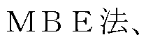


Claims
Priority Applications (4)
| Application Number | Priority Date | Filing Date | Title |
|---|---|---|---|
| CN202080016065.9A CN113491006B (zh) | 2019-02-28 | 2020-02-18 | 半导体装置及半导体装置的制造方法 |
| KR1020217028554A KR102744478B1 (ko) | 2019-02-28 | 2020-02-18 | 반도체 장치 및 반도체 장치의 제작 방법 |
| JP2021501136A JP7314249B2 (ja) | 2019-02-28 | 2020-02-18 | 半導体装置 |
| US17/428,825 US12349403B2 (en) | 2019-02-28 | 2020-02-18 | Semiconductor device comprising oxygen blocking films |
Applications Claiming Priority (2)
| Application Number | Priority Date | Filing Date | Title |
|---|---|---|---|
| JP2019-035103 | 2019-02-28 | ||
| JP2019035103 | 2019-02-28 |
Publications (1)
| Publication Number | Publication Date |
|---|---|
| WO2020174315A1 true WO2020174315A1 (ja) | 2020-09-03 |
Family
ID=72239233
Family Applications (1)
| Application Number | Title | Priority Date | Filing Date |
|---|---|---|---|
| PCT/IB2020/051316 Ceased WO2020174315A1 (ja) | 2019-02-28 | 2020-02-18 | 半導体装置、および半導体装置の作製方法 |
Country Status (5)
| Country | Link |
|---|---|
| US (1) | US12349403B2 (ja) |
| JP (1) | JP7314249B2 (ja) |
| KR (1) | KR102744478B1 (ja) |
| CN (1) | CN113491006B (ja) |
| WO (1) | WO2020174315A1 (ja) |
Cited By (2)
| Publication number | Priority date | Publication date | Assignee | Title |
|---|---|---|---|---|
| WO2024154036A1 (ja) * | 2023-01-20 | 2024-07-25 | 株式会社半導体エネルギー研究所 | 半導体装置 |
| TWI914289B (zh) | 2022-04-30 | 2026-02-01 | 美商佩利達斯股份有限公司 | P型碳化矽與低電阻率碳化矽之晶體、晶棒、晶圓與元件及其製造方法 |
Citations (6)
| Publication number | Priority date | Publication date | Assignee | Title |
|---|---|---|---|---|
| JP2015053477A (ja) * | 2013-08-05 | 2015-03-19 | 株式会社半導体エネルギー研究所 | 半導体装置および半導体装置の作製方法 |
| JP2015156477A (ja) * | 2013-12-26 | 2015-08-27 | 株式会社半導体エネルギー研究所 | 半導体装置、および電子機器 |
| JP2015181162A (ja) * | 2014-03-06 | 2015-10-15 | 株式会社半導体エネルギー研究所 | 半導体装置の作製方法 |
| JP2015181151A (ja) * | 2014-02-05 | 2015-10-15 | 株式会社半導体エネルギー研究所 | 半導体装置およびその作製方法 |
| JP2017034258A (ja) * | 2015-08-03 | 2017-02-09 | 株式会社半導体エネルギー研究所 | 半導体装置、半導体装置の作製方法、および電子機器 |
| JP2018067708A (ja) * | 2016-10-14 | 2018-04-26 | 株式会社半導体エネルギー研究所 | 半導体装置およびその作製方法 |
Family Cites Families (16)
| Publication number | Priority date | Publication date | Assignee | Title |
|---|---|---|---|---|
| JP6300489B2 (ja) * | 2012-10-24 | 2018-03-28 | 株式会社半導体エネルギー研究所 | 半導体装置の作製方法 |
| TWI644433B (zh) * | 2013-03-13 | 2018-12-11 | 半導體能源研究所股份有限公司 | 半導體裝置 |
| JP6322503B2 (ja) * | 2013-07-16 | 2018-05-09 | 株式会社半導体エネルギー研究所 | 半導体装置 |
| TWI642186B (zh) * | 2013-12-18 | 2018-11-21 | 日商半導體能源研究所股份有限公司 | 半導體裝置 |
| WO2016092427A1 (en) | 2014-12-10 | 2016-06-16 | Semiconductor Energy Laboratory Co., Ltd. | Semiconductor device and method for manufacturing the same |
| US9954112B2 (en) | 2015-01-26 | 2018-04-24 | Semiconductor Energy Laboratory Co., Ltd. | Semiconductor device and manufacturing method thereof |
| JP6887243B2 (ja) * | 2015-12-11 | 2021-06-16 | 株式会社半導体エネルギー研究所 | トランジスタ、半導体装置、電子機器及び半導ウエハ |
| JP6851814B2 (ja) * | 2015-12-29 | 2021-03-31 | 株式会社半導体エネルギー研究所 | トランジスタ |
| KR20170096956A (ko) | 2016-02-17 | 2017-08-25 | 가부시키가이샤 한도오따이 에네루기 켄큐쇼 | 반도체 장치, 전자 기기 |
| US9978879B2 (en) | 2016-08-31 | 2018-05-22 | Semiconductor Energy Laboratory Co., Ltd. | Semiconductor device |
| JP2018201011A (ja) * | 2017-05-26 | 2018-12-20 | 株式会社半導体エネルギー研究所 | 半導体装置、および半導体装置の作製方法 |
| JP2018206828A (ja) | 2017-05-31 | 2018-12-27 | 株式会社半導体エネルギー研究所 | 半導体装置、および半導体装置の作製方法 |
| WO2019016642A1 (ja) | 2017-07-21 | 2019-01-24 | 株式会社半導体エネルギー研究所 | 半導体装置、および半導体装置の作製方法 |
| CN111081773B (zh) * | 2018-10-18 | 2023-03-24 | 联华电子股份有限公司 | 氧化物半导体装置以及其制作方法 |
| CN113330553A (zh) | 2019-01-29 | 2021-08-31 | 株式会社半导体能源研究所 | 半导体装置以及半导体装置的制造方法 |
| KR102948551B1 (ko) * | 2019-06-14 | 2026-04-03 | 가부시키가이샤 한도오따이 에네루기 켄큐쇼 | 반도체 장치 및 반도체 장치의 제작 방법 |
-
2020
- 2020-02-18 CN CN202080016065.9A patent/CN113491006B/zh active Active
- 2020-02-18 JP JP2021501136A patent/JP7314249B2/ja active Active
- 2020-02-18 US US17/428,825 patent/US12349403B2/en active Active
- 2020-02-18 WO PCT/IB2020/051316 patent/WO2020174315A1/ja not_active Ceased
- 2020-02-18 KR KR1020217028554A patent/KR102744478B1/ko active Active
Patent Citations (6)
| Publication number | Priority date | Publication date | Assignee | Title |
|---|---|---|---|---|
| JP2015053477A (ja) * | 2013-08-05 | 2015-03-19 | 株式会社半導体エネルギー研究所 | 半導体装置および半導体装置の作製方法 |
| JP2015156477A (ja) * | 2013-12-26 | 2015-08-27 | 株式会社半導体エネルギー研究所 | 半導体装置、および電子機器 |
| JP2015181151A (ja) * | 2014-02-05 | 2015-10-15 | 株式会社半導体エネルギー研究所 | 半導体装置およびその作製方法 |
| JP2015181162A (ja) * | 2014-03-06 | 2015-10-15 | 株式会社半導体エネルギー研究所 | 半導体装置の作製方法 |
| JP2017034258A (ja) * | 2015-08-03 | 2017-02-09 | 株式会社半導体エネルギー研究所 | 半導体装置、半導体装置の作製方法、および電子機器 |
| JP2018067708A (ja) * | 2016-10-14 | 2018-04-26 | 株式会社半導体エネルギー研究所 | 半導体装置およびその作製方法 |
Cited By (2)
| Publication number | Priority date | Publication date | Assignee | Title |
|---|---|---|---|---|
| TWI914289B (zh) | 2022-04-30 | 2026-02-01 | 美商佩利達斯股份有限公司 | P型碳化矽與低電阻率碳化矽之晶體、晶棒、晶圓與元件及其製造方法 |
| WO2024154036A1 (ja) * | 2023-01-20 | 2024-07-25 | 株式会社半導体エネルギー研究所 | 半導体装置 |
Also Published As
| Publication number | Publication date |
|---|---|
| CN113491006B (zh) | 2025-09-23 |
| KR20210130167A (ko) | 2021-10-29 |
| US12349403B2 (en) | 2025-07-01 |
| US20220020883A1 (en) | 2022-01-20 |
| KR102744478B1 (ko) | 2024-12-18 |
| CN113491006A (zh) | 2021-10-08 |
| JP7314249B2 (ja) | 2023-07-25 |
| JPWO2020174315A1 (ja) | 2020-09-03 |
Similar Documents
| Publication | Publication Date | Title |
|---|---|---|
| JP2025000933A (ja) | 半導体装置 | |
| TWI856139B (zh) | 半導體裝置 | |
| JP7555906B2 (ja) | 半導体装置の作製方法 | |
| WO2020201870A1 (ja) | 半導体装置、および半導体装置の作製方法 | |
| KR20220031020A (ko) | 반도체 장치 및 반도체 장치의 제작 방법 | |
| KR20220124700A (ko) | 반도체 장치 및 반도체 장치의 제작 방법 | |
| JP7628956B2 (ja) | 半導体装置 | |
| TWI858071B (zh) | 半導體裝置以及半導體裝置的製造方法 | |
| WO2020229914A1 (ja) | 半導体装置、および半導体装置の作製方法 | |
| WO2024116037A1 (ja) | 半導体装置 | |
| JP2025164843A (ja) | 記憶装置 | |
| JPWO2019111106A1 (ja) | 半導体装置、および半導体装置の作製方法 | |
| TW202335185A (zh) | 記憶體裝置 | |
| WO2023126741A1 (ja) | 半導体装置、記憶装置、及び半導体装置の作製方法 | |
| JPWO2020049420A1 (ja) | 半導体装置、および半導体装置の作製方法 | |
| JPWO2019224656A1 (ja) | 半導体装置、および半導体装置の作製方法 | |
| JP7314249B2 (ja) | 半導体装置 | |
| KR102811827B1 (ko) | 반도체 장치 및 반도체 장치의 제작 방법 | |
| JP7771265B2 (ja) | 半導体装置 | |
| JP7721699B2 (ja) | 半導体装置 | |
| CN116097401A (zh) | 绝缘膜的改性方法及半导体装置的制造方法 | |
| WO2020183277A1 (ja) | 半導体装置、及び半導体装置の作製方法 | |
| WO2024042419A1 (ja) | 記憶装置 | |
| JP7586825B2 (ja) | 半導体装置 | |
| KR20220120577A (ko) | 반도체 장치, 반도체 장치의 제작 방법 |
Legal Events
| Date | Code | Title | Description |
|---|---|---|---|
| 121 | Ep: the epo has been informed by wipo that ep was designated in this application |
Ref document number: 20762533 Country of ref document: EP Kind code of ref document: A1 |
|
| ENP | Entry into the national phase |
Ref document number: 2021501136 Country of ref document: JP Kind code of ref document: A |
|
| NENP | Non-entry into the national phase |
Ref country code: DE |
|
| ENP | Entry into the national phase |
Ref document number: 20217028554 Country of ref document: KR Kind code of ref document: A |
|
| 122 | Ep: pct application non-entry in european phase |
Ref document number: 20762533 Country of ref document: EP Kind code of ref document: A1 |
|
| WWG | Wipo information: grant in national office |
Ref document number: 17428825 Country of ref document: US |
|
| WWG | Wipo information: grant in national office |
Ref document number: 202080016065.9 Country of ref document: CN |