WO2020170871A1 - 光変調器 - Google Patents
光変調器 Download PDFInfo
- Publication number
- WO2020170871A1 WO2020170871A1 PCT/JP2020/004954 JP2020004954W WO2020170871A1 WO 2020170871 A1 WO2020170871 A1 WO 2020170871A1 JP 2020004954 W JP2020004954 W JP 2020004954W WO 2020170871 A1 WO2020170871 A1 WO 2020170871A1
- Authority
- WO
- WIPO (PCT)
- Prior art keywords
- optical
- modulator
- traveling wave
- phase
- mach
- Prior art date
- Legal status (The legal status is an assumption and is not a legal conclusion. Google has not performed a legal analysis and makes no representation as to the accuracy of the status listed.)
- Ceased
Links
Images







Classifications
-
- G—PHYSICS
- G02—OPTICS
- G02F—OPTICAL DEVICES OR ARRANGEMENTS FOR THE CONTROL OF LIGHT BY MODIFICATION OF THE OPTICAL PROPERTIES OF THE MEDIA OF THE ELEMENTS INVOLVED THEREIN; NON-LINEAR OPTICS; FREQUENCY-CHANGING OF LIGHT; OPTICAL LOGIC ELEMENTS; OPTICAL ANALOGUE/DIGITAL CONVERTERS
- G02F1/00—Devices or arrangements for the control of the intensity, colour, phase, polarisation or direction of light arriving from an independent light source, e.g. switching, gating or modulating; Non-linear optics
- G02F1/01—Devices or arrangements for the control of the intensity, colour, phase, polarisation or direction of light arriving from an independent light source, e.g. switching, gating or modulating; Non-linear optics for the control of the intensity, phase, polarisation or colour
- G02F1/21—Devices or arrangements for the control of the intensity, colour, phase, polarisation or direction of light arriving from an independent light source, e.g. switching, gating or modulating; Non-linear optics for the control of the intensity, phase, polarisation or colour by interference
- G02F1/212—Mach-Zehnder type
-
- G—PHYSICS
- G02—OPTICS
- G02F—OPTICAL DEVICES OR ARRANGEMENTS FOR THE CONTROL OF LIGHT BY MODIFICATION OF THE OPTICAL PROPERTIES OF THE MEDIA OF THE ELEMENTS INVOLVED THEREIN; NON-LINEAR OPTICS; FREQUENCY-CHANGING OF LIGHT; OPTICAL LOGIC ELEMENTS; OPTICAL ANALOGUE/DIGITAL CONVERTERS
- G02F1/00—Devices or arrangements for the control of the intensity, colour, phase, polarisation or direction of light arriving from an independent light source, e.g. switching, gating or modulating; Non-linear optics
- G02F1/01—Devices or arrangements for the control of the intensity, colour, phase, polarisation or direction of light arriving from an independent light source, e.g. switching, gating or modulating; Non-linear optics for the control of the intensity, phase, polarisation or colour
- G02F1/015—Devices or arrangements for the control of the intensity, colour, phase, polarisation or direction of light arriving from an independent light source, e.g. switching, gating or modulating; Non-linear optics for the control of the intensity, phase, polarisation or colour based on semiconductor elements having potential barriers, e.g. having a PN or PIN junction
-
- G—PHYSICS
- G02—OPTICS
- G02F—OPTICAL DEVICES OR ARRANGEMENTS FOR THE CONTROL OF LIGHT BY MODIFICATION OF THE OPTICAL PROPERTIES OF THE MEDIA OF THE ELEMENTS INVOLVED THEREIN; NON-LINEAR OPTICS; FREQUENCY-CHANGING OF LIGHT; OPTICAL LOGIC ELEMENTS; OPTICAL ANALOGUE/DIGITAL CONVERTERS
- G02F1/00—Devices or arrangements for the control of the intensity, colour, phase, polarisation or direction of light arriving from an independent light source, e.g. switching, gating or modulating; Non-linear optics
- G02F1/01—Devices or arrangements for the control of the intensity, colour, phase, polarisation or direction of light arriving from an independent light source, e.g. switching, gating or modulating; Non-linear optics for the control of the intensity, phase, polarisation or colour
- G02F1/015—Devices or arrangements for the control of the intensity, colour, phase, polarisation or direction of light arriving from an independent light source, e.g. switching, gating or modulating; Non-linear optics for the control of the intensity, phase, polarisation or colour based on semiconductor elements having potential barriers, e.g. having a PN or PIN junction
- G02F1/025—Devices or arrangements for the control of the intensity, colour, phase, polarisation or direction of light arriving from an independent light source, e.g. switching, gating or modulating; Non-linear optics for the control of the intensity, phase, polarisation or colour based on semiconductor elements having potential barriers, e.g. having a PN or PIN junction in an optical waveguide structure
-
- G—PHYSICS
- G02—OPTICS
- G02F—OPTICAL DEVICES OR ARRANGEMENTS FOR THE CONTROL OF LIGHT BY MODIFICATION OF THE OPTICAL PROPERTIES OF THE MEDIA OF THE ELEMENTS INVOLVED THEREIN; NON-LINEAR OPTICS; FREQUENCY-CHANGING OF LIGHT; OPTICAL LOGIC ELEMENTS; OPTICAL ANALOGUE/DIGITAL CONVERTERS
- G02F1/00—Devices or arrangements for the control of the intensity, colour, phase, polarisation or direction of light arriving from an independent light source, e.g. switching, gating or modulating; Non-linear optics
- G02F1/01—Devices or arrangements for the control of the intensity, colour, phase, polarisation or direction of light arriving from an independent light source, e.g. switching, gating or modulating; Non-linear optics for the control of the intensity, phase, polarisation or colour
- G02F1/21—Devices or arrangements for the control of the intensity, colour, phase, polarisation or direction of light arriving from an independent light source, e.g. switching, gating or modulating; Non-linear optics for the control of the intensity, phase, polarisation or colour by interference
- G02F1/225—Devices or arrangements for the control of the intensity, colour, phase, polarisation or direction of light arriving from an independent light source, e.g. switching, gating or modulating; Non-linear optics for the control of the intensity, phase, polarisation or colour by interference in an optical waveguide structure
- G02F1/2257—Devices or arrangements for the control of the intensity, colour, phase, polarisation or direction of light arriving from an independent light source, e.g. switching, gating or modulating; Non-linear optics for the control of the intensity, phase, polarisation or colour by interference in an optical waveguide structure the optical waveguides being made of semiconducting material
-
- G—PHYSICS
- G02—OPTICS
- G02F—OPTICAL DEVICES OR ARRANGEMENTS FOR THE CONTROL OF LIGHT BY MODIFICATION OF THE OPTICAL PROPERTIES OF THE MEDIA OF THE ELEMENTS INVOLVED THEREIN; NON-LINEAR OPTICS; FREQUENCY-CHANGING OF LIGHT; OPTICAL LOGIC ELEMENTS; OPTICAL ANALOGUE/DIGITAL CONVERTERS
- G02F2201/00—Constructional arrangements not provided for in groups G02F1/00 - G02F7/00
- G02F2201/12—Constructional arrangements not provided for in groups G02F1/00 - G02F7/00 electrode
- G02F2201/127—Constructional arrangements not provided for in groups G02F1/00 - G02F7/00 electrode travelling wave
Definitions
- the present invention relates to an optical modulator, and more particularly to an optical modulator capable of high-quality modulation of an optical transmission signal.
- the Mach-Zehnder optical modulator splits the light incident on the input side optical waveguide into two optical waveguides (arm optical waveguides) with a 1:1 intensity, propagates the branched light for a certain length, and then combines them again. It has a structure to output by wave. By changing the phase of the two lights by the phase modulator provided in the optical waveguide branched into two, the interference condition of the lights when they are combined is changed, and the intensity or phase of the output light is modulated. be able to. Mach-Zehnder optical modulators are widely used in medium- and long-distance optical communications over metro distances because they have small wavelength dependence, have no wavelength chirp component in principle, and are faster.
- a dielectric such as LiNbO 3 or a semiconductor such as InP, GaAs or Si (silicon) is used as a material forming the optical waveguide of the phase modulation section, and a modulated electric signal is applied to electrodes arranged near these optical waveguides.
- a voltage By inputting and applying a voltage to the optical waveguide, the phase of light propagating through the optical waveguide is changed.
- Si is used as the optical waveguide
- a photodiode using Ge (germanium) capable of crystal growth on a Si substrate, a directional coupler using the Si optical waveguide, , Y-splitters and other passive optical circuits can be integrated together. Therefore, it is possible to reduce the size of devices required for transmitting and receiving optical communication into a single chip, so research and development have been actively conducted in recent years for application to next-generation optical transmitters, receivers, and optical transceivers. Has been done in.
- a Si optical modulator is composed of an SOI (Silicon on Insulator) substrate in which a Si thin film is adhered on an oxide film (Buried Oxide: BOX) layer obtained by thermally oxidizing the surface of a Si substrate, and light is guided through the SOI layer.
- SOI Silicon on Insulator
- BOX oxide film
- a dopant is injected so as to be a p-type or n-type semiconductor, SiO 2 to be a clad layer for light is deposited, electrodes are formed, and the like is manufactured.
- FIG. 1 shows a cross-sectional structure diagram of an optical waveguide of an optical phase modulator having a lateral PN junction which is the basis of a conventional Si optical modulator.
- the phase modulator of this Si optical modulator is composed of the Si layer 2 sandwiched between the upper and lower SiO 2 cladding layers 1 and 3, and the Si thin line for confining light in the center of the figure has ribs with different thicknesses. It has a structure called a waveguide.
- the central thick portion of the Si layer 2 in FIG. 1 is used as a waveguide core 20, and an optical waveguide 7 for confining light propagating in the direction perpendicular to the paper surface is constructed by utilizing the difference in refractive index between the surrounding SiO 2 cladding layers 1 and 3. To do.
- a high-concentration p-type semiconductor layer 22 and a high-concentration n-type semiconductor layer 23 are provided in the slab regions 21 on both sides of the optical waveguide 7, and a medium-concentration p-type semiconductor layer 24 and a medium-concentration n-type semiconductor layer 24 are provided in the center of the core of the optical waveguide 7.
- a pn junction structure is formed by the type semiconductor layer 25, and a modulation electric signal and a bias are applied from the left and right ends of FIG.
- the pn junction structure formed by the medium-concentration p-type semiconductor layer 24 and the medium-concentration n-type semiconductor layer 25 may be a pin structure with an undoped i-type (intrinsic) semiconductor interposed therebetween.
- one of a p-type semiconductor and an n-type semiconductor is arbitrarily referred to as a region having a first polarity and the other is referred to as a region having a second polarity regardless of the concentration. be able to.
- metal electrodes shown in air in contact with the high-concentration semiconductor layers 22 and 23 at both ends are provided, and a reverse bias electric field (Fig. In the case of 1, right to left) is applied.
- a reverse bias electric field Fig. In the case of 1, right to left
- the carrier density inside the optical waveguide core 20 is changed, and the refractive index of the optical waveguide is changed (carrier plasma effect), whereby the phase of light can be modulated.
- the waveguide size depends on the refractive index of the material to be the core/clad, and therefore cannot be uniquely determined.
- the rib type silicon waveguide structure including the optical waveguide core 20 and the slab regions 21 on both sides as shown in FIG. 1 is used.
- the core has a width of 400 to 600 (nm) ⁇ height of 150 to 300 (nm)
- the slab has a thickness of 50 to 200 (nm) and a length (mm). ..
- a traveling-wave electrode type Mach-Zehnder optical modulator is a broadband Mach-Zehnder optical modulator having a band of 10 Gbps or more.
- the traveling wave electrode is an electrode that matches the velocity (phase velocity matching) between the modulated electric signal (microwave and high frequency signal) and the light (light wave) propagating in the optical waveguide, and interacts with the light while propagating the electric signal.
- Non-Patent Document 1 is a report example of a Si Mach-Zehnder optical modulator using a traveling wave type electrode having a length of about several millimeters.
- FIG. 2 shows a typical traveling-wave electrode type Mach-Zehnder optical modulator.
- FIG. 3 shows a sectional structure of the traveling wave electrode type Mach-Zehnder optical modulator taken along the section line III-III′ in FIG.
- the traveling wave electrode type Mach-Zehnder optical modulator includes an input optical coupler (or Y-shaped splitter) 101, and a pair of parallel first and second waveguides 102 and 102 for guiding the input light branched into two. Of the optical waveguide 103 and an output optical coupler 104 that couples the output lights of these.
- the waveguides 102 and 103 are rib waveguides, and are regions 105 having a first polarity and regions having a second polarity in the vertical direction of the drawing, as described above with reference to FIG.
- An optical phase modulation unit divided into 106 is configured. Either the region having the first polarity or the region having the second polarity of the phase modulator of the first waveguide 102 and the second waveguide 103 is formed in the region surrounded by the waveguides 102 and 103. There is.
- FIG. 2 shows a case where the region 106 having the second polarity is formed in the region surrounded by the waveguides 102 and 103.
- the region 105 having the first polarity is formed in the opposite direction to the region 106 having the second polarity with the light traveling direction of each phase modulator as an axis.
- a metal bias electrode 107 is provided in the region 106 having the second polarity, and a traveling wave electrode 108 is provided in each of the two regions 105 having the first polarity in the vertical direction of the paper.
- the metal bias electrode 107 is applied with a voltage such that the PN junction is in the reverse bias state regardless of the bias state of each of the pair of traveling wave electrodes 108. Then, the traveling wave electrode 108 is applied with a differential voltage from the left side of the drawing as a high frequency modulated electric signal (RF signal) to modulate light.
- RF signal high frequency modulated electric signal
- the traveling wave electrode 108 is provided with an input side pad 109 for connecting an output signal from a driver for driving the modulator by wire bonding or the like. Further, an output side pad 110 is provided for connecting with a terminating resistor for impedance matching and terminating a high frequency signal.
- FIG. 4 shows a connection diagram in which the driver 50 and the terminating resistor 51 and the Mach-Zehnder optical modulator are combined.
- the traveling wave electrode 108 of the Mach-Zehnder optical modulator is connected to the terminal 516 (potential of the power supply) via the terminating resistor 51. If the output impedance Rout of the driver 50, the characteristic impedance Z of the traveling wave electrode 108 of the optical modulator, and the resistance value Rterm of the terminating resistor 51 are equal, impedance matching is achieved, and the signal output from the driver 50 is reflected. It is terminated by the terminating resistor 51 without doing so, and the best high frequency characteristics of the optical modulator can be expected. Therefore, generally, the values of Rout, Z, and Rterm are designed to be equal to each other.
- Rout depends on the driver design
- Z depends on the modulator design.
- Rterm deviates from an ideal value due to process variations and variations as members.
- FIG. 5 shows the EO (optical output) characteristics of the Mach-Zehnder optical modulator when the values of Rout, Z, and Rterm are changed.
- FIG. 5 shows a case where Rout is higher than Z by about 150 ohms with respect to Z, and when the value of Rterm is the same value as Z, ⁇ 5 and ⁇ 10 ohms are changed from Z. It can be seen that the greater the mismatch between Rout, Z, and Rterm, the greater the ripple in the frequency characteristics.
- the ripple should be designed to be as small as possible, but it is difficult to completely eliminate the ripple from the above reason.
- the reflected signal generated by the mismatch between Z and Rterm is Since the light is reflected at the output end of the driver without being substantially attenuated, a slight mismatch between Z and Rterm tends to increase the amount of ripples, resulting in deterioration of the quality of the transmission signal.
- the present invention has been made in view of such a problem, and an object of the present invention is to provide an optical modulator in which the amount of ripple is reduced without affecting the modulation characteristics.
- an aspect of the present invention is an optical modulator formed on a substrate and having at least one optical input, at least one optical output, and at least one phase modulator. ..
- the phase modulator applies the high frequency signal for modulation to the optical waveguide having the PN junction structure, and the light propagating through the optical waveguide interacts while propagating in the same direction.
- the traveling wave electrode is formed longer in the light propagation direction of the phase modulation section than the phase modulation section, and constitutes the attenuation region.
- the attenuation region is a dummy phase modulator, and the dummy phase modulator has a portion formed longer than the phase modulator of the traveling wave electrode and the same PN junction structure as the optical waveguide of the phase modulator. A part of the optical waveguide and an optical waveguide which is not connected.
- Another aspect of the present invention is an optical transmitter including the above optical modulator.
- the traveling wave electrode included in the optical modulator due to the structure of the traveling wave electrode included in the optical modulator, a region for reducing the ripple is provided so that the EO band characteristic is not deteriorated and the optical output intensity is not deteriorated. In addition, it is possible to reduce only the ripple amount and improve the quality of the transmission signal.
- (A) is a schematic top view of a state in which a driver, a traveling wave electrode type Mach-Zehnder optical modulator and a terminating resistor are connected, and
- (b) is a side view. It is an EO characteristic when a conventional traveling wave electrode type Mach-Zehnder optical modulator is used.
- FIG. 3 is an EO characteristic of a traveling wave electrode type Mach-Zehnder optical modulator according to an embodiment of the present invention. It is a schematic diagram of a traveling wave electrode type Mach-Zehnder optical modulator according to an embodiment of the present invention. It is a schematic diagram of a traveling wave electrode type Mach-Zehnder optical modulator according to an embodiment of the present invention. It is a schematic diagram of a traveling wave electrode type Mach-Zehnder optical modulator according to an embodiment of the present invention. It is a schematic diagram of a traveling wave electrode type Mach-Zehnder optical modulator according to an embodiment of the present invention. (A) is a schematic top view of a state in which a driver and a traveling wave electrode type Mach-Zehnder optical modulator according to an embodiment of the present invention are connected, and (b) is a side view.
- FIG. 6 is a plan view showing the configuration of the Mach-Zehnder optical modulator according to the first embodiment of the present invention.
- the Mach-Zehnder optical modulator of the present embodiment has a configuration obtained by improving the configuration of the conventional Mach-Zehnder optical modulator shown in FIG.
- the optical modulator shown in FIG. 6 includes an input optical coupler 101, a pair of parallel first and second waveguides 102 and 103 for guiding the input light branched from the input optical coupler 101, and two of them.
- the output optical coupler 104 for coupling the output lights of The input light is input via a linear waveguide or a bending waveguide connected to the input port of the input optical coupler 101, and also via a linear waveguide or a bending waveguide connected to the output port of the output optical coupler 104. Is output.
- the waveguides 102 and 103 are rib waveguides, and are divided into a region 105 having a first polarity and a region 106 having a second polarity in the vertical direction on the paper surface.
- the region 106 having the second polarity of the phase modulator of the first waveguide 102 and the second waveguide 103 is formed in the region surrounded by the waveguides 102 and 103.
- the regions having the first polarity of the waveguides 102 and 103 are formed in the opposite direction to the region 106 having the second polarity with the light traveling direction of each phase modulation section as an axis.
- a metal bias electrode 107 is provided in the region 106 having the second polarity, and a traveling wave electrode 108 is provided in each of the two regions 105 having the first polarity in the vertical direction of the paper. ..
- the traveling wave electrode 108 is provided with an input side pad 109 for connecting an output signal from a driver for driving the modulator by wire bonding or the like.
- an output side pad 110 is provided for connecting with a terminating resistor for impedance matching and terminating a high frequency signal.
- the optical modulator of FIG. 6 is different from the optical modulator of the conventional example shown in FIG. 2 in that the traveling wave electrode 108 is closer to the phase modulation section in the light propagation direction of the phase modulation section than the phase modulation section. Is longer than that. Traveling wave electrode 108 generally has a characteristic of attenuating high-frequency waves as they propagate. Therefore, in FIG. 4, when the Mach-Zehnder optical modulator connected to the driver 50 and the terminating resistor 51 is replaced with the Mach-Zehnder optical modulator in FIG. 6, multiple reflection between Rout and Rterm can be reduced. .. Therefore, it is possible to reduce ripples and improve the quality of the transmission signal.
- FIG. 7 shows the EO (optical output) characteristics of the conventional optical modulator of FIG. 2 and the optical modulator of FIG. It can be seen that the optical modulator of FIG. 6 can suppress the amount of ripple even when the value of Rterm is higher than Z by 10 ohm.
- FIG. 7 is an example calculated as an example in which the characteristics of the traveling wave electrode in the latter half region (attenuation region) of the phase modulation unit have an attenuation of about 3 dB at 10 GHz.
- the attenuation area must be provided in the latter half of the phase modulation section in the light propagation direction of the phase modulation section.
- the attenuation region is provided in the first half of the phase modulation unit in the optical propagation direction of the phase modulation unit, the high frequency electrical modulation signal input from the driver through the input side pad 109 is attenuated in the attenuation region and then the phase modulation unit is activated. Since it propagates and obtains an optical modulation effect, it becomes a cause of impairing the modulation performance.
- the traveling wave electrode 108 has the same shape in the phase modulator and the attenuation region, but the shape may be changed in the phase modulator and the attenuation region.
- a traveling wave electrode when a traveling wave electrode is loaded with a phase modulator (in a Si Mach-Zehnder modulator, a PN junction is used as the phase modulator), the impedance is lowered. Therefore, it is necessary to match the impedances of the phase modulator and the attenuation region.
- FIG. 8 is a plan view showing the configuration of the Mach-Zehnder optical modulator according to the second embodiment of the present invention.
- the optical modulator of the present embodiment includes an input optical coupler 101, a pair of parallel first and second waveguides 102 and 103 for guiding input light branched from the input optical coupler 101, and two of them.
- the output optical coupler 104 for coupling the output lights of The waveguides 102 and 103 are rib waveguides, and are divided into a region 105 having a first polarity and a region 106 having a second polarity in the vertical direction on the paper surface.
- the input light is input through a straight waveguide or a bending waveguide connected to the input port of the input optical coupler 101, and also through a straight waveguide or a bending waveguide connected to the output port of the output optical coupler 104. Is output. Traveling wave electrode 108 is formed longer than the phase modulation section in the light propagation direction of the phase modulation section, and constitutes an attenuation region. A metal bias electrode 107 is provided in the region 106 having the second polarity.
- the Mach-Zehnder optical modulator according to this embodiment has a configuration that enables impedance matching between the phase modulator and the attenuation region.
- the traveling wave electrode 108 has a width in the attenuation region larger than that in the phase modulator.
- the impedance can be lowered by narrowing the electrode spacing between the two traveling wave electrodes, and impedance matching between the phase modulator and the attenuation region can be achieved.
- FIG. 9 is a plan view showing the configuration of a Mach-Zehnder optical modulator according to the third embodiment of the present invention.
- the optical modulator of the present embodiment includes an input optical coupler 101, a pair of parallel first and second waveguides 102 and 103 that guide the input light branched into two, and The output optical coupler 104 for coupling the output lights of
- the waveguides 102 and 103 are rib waveguides, and are divided into a region 105 having a first polarity and a region 106 having a second polarity in the vertical direction of the paper surface.
- the input light is input via a linear waveguide or a bending waveguide connected to the input port of the input optical coupler 101, and also via a linear waveguide or a bending waveguide connected to the output port of the output optical coupler 104. Is output.
- the traveling wave electrode 108 is provided between the input optical coupler 101 and the output optical coupler 104 to form a phase modulator.
- a metal bias electrode 107 is provided in the region 106 having the second polarity.
- the traveling wave electrode forming the phase modulator is extended to form an attenuation region having an attenuation action, thereby reducing the amount of ripple and improving the quality of the transmission signal. Got the effect of improving.
- the Mach-Zehnder optical modulator according to the present embodiment has a configuration in which the fixed attenuator 52 is installed between the traveling wave electrode 108 and the pad 110.
- the fixed attenuator 52 it is possible to generate the damping action without extending the traveling wave electrode 108 forming the phase modulator. As a result, the ripple amount of the EO characteristic can be suppressed.
- the fixed attenuator 52 can be installed by surface-mounting a small attenuator as a chip member on the modulator.
- FIG. 10 is a plan view showing the configuration of the Mach-Zehnder optical modulator according to the fourth embodiment of the present invention.
- the optical modulator of the present embodiment includes an input optical coupler 101, a pair of parallel first and second waveguides 102 and 103 that guide the input light branched into two, and The output optical coupler 104 for coupling the output lights of The input light is input via a straight waveguide or a bending waveguide connected to the input port of the input optical coupler 101, and is output via a bending waveguide connected to the output port of the output optical coupler 104. ..
- the waveguides 102 and 103 are rib waveguides, and are divided into a region 105 having a first polarity and a region 106 having a second polarity in the vertical direction on the paper surface. Traveling wave electrode 108 is formed longer than the phase modulation section in the light propagation direction of the phase modulation section. A metal bias electrode 107 is provided in the region 106 having the second polarity.
- the Mach-Zehnder optical modulator according to the present embodiment does not have a fixed attenuator as a separate chip member like the Mach-Zehnder optical modulator shown in FIG. 9, but has a dummy phase modulator 53 formed monolithically on silicon photonics. It is a composition.
- the dummy phase modulator 53 plays the role of a fixed attenuator having a large damping action.
- the dummy phase modulator 53 monolithically formed on silicon photonics also has a phase modulation with one to two parallel waveguides (in the optical propagation directions of the first waveguide 102 and the second waveguide 103). And a traveling wave electrode 108 formed longer than the phase modulation part in the light propagation direction of the part.
- the one-to-two parallel waveguides of the dummy phase modulator 53 are also rib waveguides, and are divided into regions having the first polarity and regions having the second polarity.
- a metal bias electrode 54 is provided in the region having the second polarity.
- the sectional structure of the dummy phase modulator 53 is the same as that of the phase modulator shown in FIG. 3, but is not connected to the output of the Mach-Zehnder optical modulator.
- a traveling wave electrode loaded with a PN junction has a large attenuation characteristic when passing a high frequency wave, and thus can be used as a fixed attenuator.
- the Mach-Zehnder optical modulator of the present embodiment has a mounting cost and components. The number of points can be reduced and the cost can be reduced. Furthermore, the doping concentrations of the region 105 having the first polarity and the region 106 having the second polarity of the dummy phase modulation unit 53 are set to the regions 105 having the first polarity and the region having the second polarity of the phase modulation unit 53. If the doping concentration is higher than the doping concentration of 106, the amount of attenuation of the traveling wave electrode 108 connected to the dummy phase modulator 53 increases, and the amount of ripple can be suppressed while reducing the size.
- the optical waveguide core 20 and the slab region 21 are PN junctions using only the high-concentration p-type semiconductor layer (p++) and the high-concentration n-type semiconductor layer (n++). Therefore, the damping action can be obtained more efficiently. Further, as described above with reference to FIG. 8, by adjusting the width and the electrode interval of the traveling wave electrode 108 in the dummy phase modulator 53, the impedance matching between the phase modulator and the dummy phase modulator is matched. be able to. As a result, it is possible to transmit light with good signal quality without ripples.
- the configuration in which the bias electrode 54 is provided in the dummy phase modulator 53 is shown, but the bias electrode 54 may be omitted.
- the depletion layer of the PN junction can be changed by changing the voltage for reverse biasing the bias electrode 54, and the attenuation amount and the impedance in the dummy phase modulator 53 can be changed.
- the reverse bias is large, the depletion layer is wide open, so the capacitance is small and the amount of attenuation is small, but the impedance is large.
- the dummy phase modulation unit 53 is provided, high frequency reflection may occur due to impedance mismatch between the phase modulation unit and the dummy phase modulation unit 53, and ripple may occur.
- the amount of attenuation of the dummy phase modulator 53 can be controlled while adjusting the ripple that may occur due to the impedance mismatch between the phase modulator and the dummy phase modulator described above by the bias. , It is possible to adjust the bias to reduce the ripple as a whole as the whole modulator.
- this effect can be adjusted even when the impedance characteristic of the dummy phase modulation section 53 varies after the Mach-Zehnder optical modulator is manufactured. Therefore, adjustment is performed so that the ripple is reduced as a whole of the modulator. Is possible.
- FIG. 11 is a plan view showing an optical transmitter according to the fifth embodiment of the present invention.
- the optical transmitter of the present embodiment is an optical transmitter using the Mach-Zehnder optical modulator according to the fourth embodiment of the present invention described with reference to FIG.
- the configuration of FIG. It is characterized in that the traveling wave electrode 108 of the Mach-Zehnder optical modulator shown in FIG. 10 is connected to the terminal 516 (potential of the power supply) without passing through 51.
- the Mach-Zehnder optical modulator shown in FIG. 8 or 9 may be used instead of the Mach-Zehnder optical modulator shown in FIG.
- impedance mismatch in Rout, Z, and Rterm causes a large ripple in the high-frequency characteristics of the optical modulator. I will have.
- the connection is made via the terminal 516 without using the termination resistor 51.
- the ripple amount can be reduced. Therefore, since the ripple can be reduced even when the terminating resistor 51 is not used, the number of parts can be reduced and the cost can be reduced without sacrificing the signal quality of the optical transmitter. Further, by reducing the number of parts, the product reliability of the optical transmitter can be improved and the yield can be improved by mounting.
Landscapes
- Physics & Mathematics (AREA)
- Nonlinear Science (AREA)
- General Physics & Mathematics (AREA)
- Optics & Photonics (AREA)
- Optical Modulation, Optical Deflection, Nonlinear Optics, Optical Demodulation, Optical Logic Elements (AREA)
Abstract
リップル量を低減させた光変調器を提供する。マッハツェンダ光変調器において、PN接合構造を有する光導波路(102,103)、及び進行波電極(108)を備えた位相変調部と、位相変調部の光伝搬方向に当該位相変調部よりも長く形成された進行波電極の部分、及び位相変調部の光導波路と同じPN接合構造を有し、位相変調部の光導波路と接続されない光導波路を備えたダミー位相変調部(53)とを備えた。
Description
本発明は、光変調器に関し、より詳細には、光伝送信号の品質の高い変調が可能な光変調器に関する。
インターネットを基盤とするサービスの爆発的な進展に伴い、これを支える光通信の大容量化、低電力化への期待はますます高まっている。光通信を行う為には、光信号を送信する光変調機が必要である。
マッハツェンダ光変調器は、入力側の光導波路に入射した光を2つの光導波路(アーム光導波路)に1:1の強度で分岐し、分岐した光を一定の長さ伝播させた後に、再度合波させて出力する構造を持つ。2つに分岐された光導波路に設けられた位相変調部により、2つの光の位相を変化させることで、合波されるときの光の干渉条件を変え、出力光の強度や位相を変調することができる。マッハツェンダ光変調器は、波長依存性が小さく、原理的に波長チャープ成分が無く、さらに高速であることからメトロ間距離以上の中・長距離光通信に広く用いられている。
位相変調部の光導波路を構成する材料としては、LiNbO3等の誘電体、InP、GaAs、Si(シリコン)等の半導体が用いられ、これらの光導波路近傍に配置された電極に変調電気信号を入力して光導波路に電圧を印加することで、光導波路を伝搬する光の位相を変化させる。特にSiを光導波路として用いた場合には、マッハツェンダ光変調器に加え、Si基板上に結晶成長が可能なGe(ゲルマニウム)を用いたフォトダイオードや、Si光導波路を用いた方向性結合器や、Y字スプリッタ等のパッシブ光回路等と一括して集積が可能である。そのため、光通信の送受に必要なデバイス群をワンチップ化し小型化が可能であることから、次世代の光送信機、受信機、及び光送受信機への応用に向け、近年研究・開発が盛んに行われている。
例えば、Si光変調器はSi基板の表面を熱酸化した酸化膜(Buried Oxide:BOX)層上にSiの薄膜を張り付けたSOI(Silicon on Insulator)基板から構成され、SOI層を光が導波できるようSi薄膜を細線に加工した後、p型又はn型の半導体となるようドーパントを注入し、光のクラッド層となるSiO2の堆積、電極の形成等を行い作製する。このとき、光の導波路は光損失が小さくなるように設計・加工する必要があり、p型又はn型のドーピング及び電極の作製は、光の損失発生を小さく抑えるとともに、高速電気信号の反射や損失を小さく抑えるように設計・加工する必要がある。
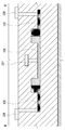
図1に、従来のSi光変調器の基本となるラテラル型のPN接合を持つ光位相変調部の光導波路の断面構造図を示す。図1では、光は紙面垂直方向に伝搬するものとする。このSi光変調器の位相変調部は、上下のSiO2クラッド層1,3に挟まれたSi層2で構成され、図中央の光を閉じ込めるためのSi細線は、厚さに差があるリブ導波路と呼ばれる構造を取っている。
図1のSi層2の中央の厚い部分を導波路コア20として、周囲のSiO2クラッド層1及び3との屈折率差を利用して紙面垂直方向に伝搬する光を閉じ込める光導波路7を構成する。
光導波路7の両側のスラブ領域21に高濃度p型半導体層22、高濃度n型半導体層23が設けられ、更に光導波路7のコア中央部には中濃度p型半導体層24、中濃度n型半導体層25によるpn接合構造が形成されて、図1の左右両端より変調電気信号とバイアスが印加されている。中濃度p型半導体層24、中濃度n型半導体層25によるpn接合構造は間にドーピングされていないi型(真性)半導体を挟んだpin構造としても良い。
なお、以下同様であるが半導体デバイスにおいて、一般的に、濃度に関わらずp型半導体及びn型半導体の一方を任意的に第1の極性を持つ領域、他方を第2の極性を持つ領域ということができる。
図1に図示は無いが、両端の高濃度半導体層22及び23に接する金属電極(風図示)を設け、金属電極よりpn接合部に、RF(高周波)の変調電気信号とともに逆バイアス電界(図1では右から左)を印加する。これにより光導波路コア20の内部のキャリア密度を変化させ、光導波路の屈折率を変えること(キャリアプラズマ効果)で、光の位相を変調することができる。
導波路寸法はコア/クラッドとなる材料の屈折率に依存するため、一意には決定できないが、図1のような光導波路コア20と両側のスラブ領域21を備えるリブ型シリコン導波路構造とした場合の一例を挙げると、導波路は、コアが幅400~600(nm)×高さ150~300(nm)、スラブは厚さ50~200(nm)で長さ数(mm)程度になる。
大容量な光通信を行うためには、高速な光変調器が必要である。10Gbps以上の帯域を持つ広帯域なマッハツェンダ光変調器として、進行波電極型マッハツェンダ光変調器がある。進行波電極は、変調電気信号(マイクロ波、高周波信号)と光導波路を伝播する光(光波)との速度を整合(位相速度整合)させ、電気信号を伝搬させながら光と相互作用を行う電極である。例えば、非特許文献1は、長さ数ミリメートル程度の進行波型電極を用いたSiマッハツェンダ光変調器の報告例である。
図2に、一般的な進行波電極型マッハツェンダ光変調器を示す。また、図3に、図2の断面線III-III’における進行波電極型マッハツェンダ光変調器の断面構造を示す。進行波電極型マッハツェンダ光変調器は、入力光カプラ(またはY字スプリッタ)101と、それより2分岐された入力光を導波する1対2本の並行する第1の導波路102及び第2の導波路103と、それらの出力光を結合する出力光カプラ104とを備える。
導波路102及び103は、図1を参照して上述した光位相変調部に関する説明のとおり、リブ導波路であり、紙面上下方向に第1の極性を持つ領域105及び第2の極性を持つ領域106に分かれた光位相変調部を構成する。第1の導波路102及び第2の導波路103の位相変調部の第1の極性を持つ領域または第2の極性を持つ領域のいずれかは導波路102及び103に囲まれる領域に形成されている。図2では、第2の極性を持つ領域106が、導波路102及び103に囲まれる領域に形成されている場合を示している。一方で、第1の極性を持つ領域105は、第2の極性を持つ領域106に対して、それぞれの位相変調部の光進行方向を軸として反対方向に形成されている。
第2の極性を持つ領域106には、金属のバイアス電極107が設けられ、紙面上下方向に2つある第1の極性を持つ領域105には、進行波電極108がそれぞれ設けられている。
Si光変調器の場合は、PN接合が逆バイアス状態でなければ、変調速度の劣化を招く。そのため、金属のバイアス電極107は、1対の進行波電極108それぞれがどのようなバイアス状態であっても、PN接合が逆バイアス状態となるような電圧を印可される。そして、進行波電極108に対して、紙面左方向から差動の電圧を高周波変調電気信号(RF信号)として印可することで、光の変調を行う。
通常、進行波電極108には、変調器を駆動する為のドライバからの出力信号をワイヤボンディング等で接続する為の、入力側パッド109が設けられる。また、インピーダンス整合をさせ、高周波信号を終端させる為の終端抵抗と接続するための、出力側パッド110が設けられる。
図4に、ドライバ50及び終端抵抗51とマッハツェンダ光変調器とを組み合わせた接続図を示す。マッハツェンダ光変調器の進行波電極108は、終端抵抗51を介して端子516(電源の電位)に接続される。ドライバ50の出力インピーダンスRout、光変調器の進行波電極108の特性インピーダンスZ、及び終端抵抗51の抵抗値Rtermがそれぞれ等しければ、インピーダンスマッチングがとれており、ドライバ50から出力された信号は、反射することなく、終端抵抗51で終端され、最も良い光変調器の高周波特性が期待できる。そのため、一般的には、Rout、Z、及びRtermの値がそれぞれ等しくなるように設計する。
David Patel, Samir Ghosh, Mathieu Chagnon, Alireza Samani,Venkat Veerasubramanian, Mohamed Osman, and David V. Plant, "Design, analysis, and transmission system performance of a 41 GHz silicon photonic modulator", Opt. Express vol.23, no.11, pp.14263-14275, 2015.
図4において、マッハツェンダ光変調器とRout、Z、及びRtermの値がそれぞれ違う場合には、インピーダンスマッチングが取れていない為に、マッハツェンダ光変調器の高周波特性が劣化する。例えば、Routはドライバの設計に依存し、Zは変調器の設計に依存するが、ドライバとマッハツェンダ光変調器をそれぞれの小型化を求めた場合のサイズ的な制約や、それぞれの特性を最大化する為に、RoutとZが異なることがある。また、Rtermがプロセスばらつきや、部材としてのばらつきによって、理想値から外れてしまう場合も起こりうる。さらには、Zは一般的に周波数特性を持つため、すべての周波数で、Rout=Z=Rtermとなるように設計することは事実上不可能である。
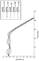
図5に、Rout、Z、及びRtermの値をそれぞれ変えた場合のマッハツェンダ光変調器のEO(光出力)特性を示す。図5では、Zを基準として、RoutがZより概ね150ohm程度高い場合に、Rtermの値をZと同じ値とした場合、Zより±5、±10ohm変化させた場合を示している。Rout、Z、及びRtermの不一致が大きくなればなるほど、周波数特性に大きなリプルを生じさせることが分かる。このような、リプルが大きい特性を持つマッハツェンダ光変調器を用いて、光変調を行った場合には、送信信号の品質が劣化する。そのため、極力リプルが小さくなるように設計すべきであるが、前述の理由から、リプルを完全になくすことは難しい。
特に、ドライバの出力抵抗を持たず、マッハツェンダ光変調器とのインピーダンスマッチングを行わないオープンコレクタ型のドライバやオープンドレイン型のドライバを用いた場合には、ZとRtermの不一致により生じた反射信号が、ドライバの出力端でほぼ減衰せずに反射する為、ZとRtermのわずかな不一致が、リップル量が増大しやすく、送信信号の品質の劣化を招いてしまう。
本発明は、このような問題に鑑みてなされたもので、その目的とするところは、変調特性に影響を与えず、リップル量を低減させた光変調器を提供することにある。
このような目的を達成するために、本発明の態様は、基板上に形成され、少なくともひとつの光入力と、少なくともひとつの光出力と、少なくともひとつの位相変調部を備えた光変調器である。一実施形態に係る光位相変調器は、位相変調部が、PN接合構造を有する光導波路と、変調用の高周波信号を印加して、光導波路を伝播する光が同一方向に伝搬しながら相互作用する進行波電極とを備え、進行波電極が、位相変調部の光伝搬方向に、当該位相変調部よりも長く形成され、減衰領域を構成する。減衰領域はダミー位相変調部であり、当該ダミー位相変調部が、進行波電極の位相変調部よりも長く形成された部分と、位相変調部の光導波路と同じPN接合構造を有し、位相変調部の光導波路と接続されない光導波路とを備える。
本端発明の別の態様は、上記光変調器を備えた光送信器である。
以上説明したように、本発明によれば、光変調器が有する進行波電極の構造により、リップルを減少させる領域を持たせることで、EO帯域特性の劣化や、光出力強度の劣化を招かずに、リップル量のみを低減させ、送信信号の品質を向上させることが可能となる。
以下、図面を参照しながら本発明の実施形態について詳細に説明する。同一または類似の符号は、同一または類似の要素を示し、繰り返しの説明は省略する。以下の説明における数値例や材料名は例示であり、本願発明は、これに限定されるものではなく、他の数値や材料で実施することができる。
(実施形態1)
図6は、本発明の第1の実施形態に係るマッハツェンダ光変調器の構成を示す平面図である。本実施形態のマッハツェンダ光変調器は、図2に示した従来例のマッハツェンダ光変調器の構成を改良した構成を有する。図6に示す光変調器は、入力光カプラ101と、それより2分岐された入力光を導波する1対2本の並行する第1の導波路102及び第2の導波路103と、それらの出力光を結合する出力光カプラ104を備える。入力光は、入力光カプラ101の入力ポートに接続された直線導波路または曲げ導波路を介して入力され、また、出力光カプラ104の出力ポートに接続された直線導波路または曲げ導波路を介して出力される。
図6は、本発明の第1の実施形態に係るマッハツェンダ光変調器の構成を示す平面図である。本実施形態のマッハツェンダ光変調器は、図2に示した従来例のマッハツェンダ光変調器の構成を改良した構成を有する。図6に示す光変調器は、入力光カプラ101と、それより2分岐された入力光を導波する1対2本の並行する第1の導波路102及び第2の導波路103と、それらの出力光を結合する出力光カプラ104を備える。入力光は、入力光カプラ101の入力ポートに接続された直線導波路または曲げ導波路を介して入力され、また、出力光カプラ104の出力ポートに接続された直線導波路または曲げ導波路を介して出力される。
導波路102及び103は、リブ導波路であり、紙面上下方向に第1の極性を持つ領域105及び第2の極性を持つ領域106に分かれている。図6では、第1の導波路102及び第2の導波路103の位相変調部の第2の極性を持つ領域106は導波路102及び103に囲まれる領域に形成されている。一方で、導波路102及び103の第1の極性を持つ領域は、第2の極性を持つ領域106に対して、それぞれの位相変調部の光進行方向を軸として反対方向に形成されている。
そして、第2の極性を持つ領域106には、金属のバイアス電極107が設けられ、紙面上下方向に2つある第1の極性を持つ領域105には、進行波電極108がそれぞれ設けられている。通常、進行波電極108には、変調器を駆動する為のドライバからの出力信号をワイヤボンディング等で接続する為の、入力側パッド109が設けられる。また、インピーダンス整合をさせ、高周波信号を終端させる為の終端抵抗と接続するための、出力側パッド110が設けられる。
図2に示した従来例の光変調器と異なる点は、図6の光変調器は、進行波電極108が位相変調部に比べて、位相変調部の光伝搬方向に向かって、位相変調部よりも長いことにある。進行波電極108は一般的に、高周波を伝搬させた場合に減衰させる特性をもつ。このため、図4において、ドライバ50及び終端抵抗51と接続されたマッハツェンダ光変調器を、図6のマッハツェンダ光変調器と置き換えた場合には、RoutとRtermの間の多重反射を減らすことができる。このため、リプルを減らし、送信信号の品質を高めることができる。
図7は、図2の従来例の光変調器と、図6の光変調器のEO(光出力)特性を示す。図6の光変調器では、Rtermの値がZよりも10ohm高い場合にも、リプル量を抑えることができていることがわかる。なお、図7は、位相変調部よりも後半の領域(減衰領域)における進行波電極の特性が、10GHzで3dB程度の減衰をもつような場合を一例として計算した例である。
また減衰領域は、位相変調部の光伝搬方向に位相変調部よりも後半に設ける必要がある。これにより、入力側パッド109を通じてドライバから入力された高周波電気変調信号が位相変調部を伝搬し光変調作用を得た後で、減衰領域で高周波信号が減衰し、出力側パッド110を通じて終端抵抗で終端される。このため、本実施形態の光変調器は、従来の光変調器と同等の光変調効果を得て、リプルを減らし、送信信号の品質を高めることができる。減衰領域を、位相変調部の光伝搬方向に位相変調部よりも前半に設けた場合には、入力側パッド109を通じてドライバから入力された高周波電気変調信号が減衰領域で減衰した後に位相変調部を伝搬し光変調作用を得ることとなるため、変調性能を損なう原因となる。
(実施形態2)
図6に示す光変調器においては進行波電極108について、位相変調部と減衰領域で同じ形状としたが、位相変調部と減衰領域で形状を変化させても良い。一般的に、変調器において、進行波電極に位相変調部を装荷した場合には(Siマッハツェンダ変調器においては、位相変調部としてPN接合を用いる)、インピーダンスが下がる。このため、位相変調部と減衰領域とのインピーダンスのマッチングとる必要がある。
図6に示す光変調器においては進行波電極108について、位相変調部と減衰領域で同じ形状としたが、位相変調部と減衰領域で形状を変化させても良い。一般的に、変調器において、進行波電極に位相変調部を装荷した場合には(Siマッハツェンダ変調器においては、位相変調部としてPN接合を用いる)、インピーダンスが下がる。このため、位相変調部と減衰領域とのインピーダンスのマッチングとる必要がある。
図8は、本発明の第2の実施形態に係るマッハツェンダ光変調器の構成を示す平面図である。本実施形態の光変調器は、入力光カプラ101と、それより2分岐された入力光を導波する1対2本の並行する第1の導波路102及び第2の導波路103と、それらの出力光を結合する出力光カプラ104を備える。導波路102及び103は、リブ導波路であり、紙面上下方向に第1の極性を持つ領域105及び第2の極性を持つ領域106に分かれている。入力光は、入力光カプラ101の入力ポートに接続された直線導波路または曲げ導波路を介して入力され、また、出力光カプラ104の出力ポートに接続された直線導波路または曲げ導波路を介して出力される。進行波電極108は、位相変調部に比べて、位相変調部の光伝搬方向に向かって、位相変調部よりも長く形成され、減衰領域を構成している。第2の極性を持つ領域106には、金属のバイアス電極107が設けられている。
本実施形態のマッハツェンダ光変調器は、位相変調部と減衰領域とのインピーダンスのマッチングをとることを可能にする構成を有する。
図8に示すように、進行波電極108は、減衰領域における幅を位相変調部における幅よりも太くしている。本実施形態の光変調器によれば、2本の進行波電極の電極間隔を狭くすることで、インピーダンスを下げることが可能とし、位相変調部と減衰領域のインピーダンスマッチングをとること可能となる。
(実施形態3)
図9は、本発明の第3の実施形態に係るマッハツェンダ光変調器の構成を示す平面図である。本実施形態の光変調器は、入力光カプラ101と、それより2分岐された入力光を導波する1対2本の並行する第1の導波路102及び第2の導波路103と、それらの出力光を結合する出力光カプラ104を備える。導波路102及び103は、リブ導波路であり、紙面上下方向に第1の極性を持つ領域105及び第2の極性を持つ領域106に分かれている。入力光は、入力光カプラ101の入力ポートに接続された直線導波路または曲げ導波路を介して入力され、また、出力光カプラ104の出力ポートに接続された直線導波路または曲げ導波路を介して出力される。進行波電極108は、入力光カプラ101と出力光カプラ104との間に設けられ位相変調部を形成している。第2の極性を持つ領域106には、金属のバイアス電極107が設けられている。
図9は、本発明の第3の実施形態に係るマッハツェンダ光変調器の構成を示す平面図である。本実施形態の光変調器は、入力光カプラ101と、それより2分岐された入力光を導波する1対2本の並行する第1の導波路102及び第2の導波路103と、それらの出力光を結合する出力光カプラ104を備える。導波路102及び103は、リブ導波路であり、紙面上下方向に第1の極性を持つ領域105及び第2の極性を持つ領域106に分かれている。入力光は、入力光カプラ101の入力ポートに接続された直線導波路または曲げ導波路を介して入力され、また、出力光カプラ104の出力ポートに接続された直線導波路または曲げ導波路を介して出力される。進行波電極108は、入力光カプラ101と出力光カプラ104との間に設けられ位相変調部を形成している。第2の極性を持つ領域106には、金属のバイアス電極107が設けられている。
第1及び第2の実施形態のマッハツェンダ光変調器では、位相変調部を構成する進行波電極を延長し、減衰作用を持つ減衰領域とすることで、リップル量を低減させ、送信信号の品質を向上する効果を得た。
本実施形態に係るマッハツェンダ光変調器は、固定減衰器52を進行波電極108とパッド110の間に設置した構成である。固定減衰器52により、位相変調部を構成する進行波電極108を延長せずとも減衰作用を生じさせられることができる。これによって、EO特性のリプル量を抑えることができる。
固定減衰器52はチップ部材の小型減衰器を変調器に表面実装して、設置することができる。
(実施形態4)
図10は、本発明の第4の実施形態に係るマッハツェンダ光変調器の構成を示す平面図である。本実施形態の光変調器は、入力光カプラ101と、それより2分岐された入力光を導波する1対2本の並行する第1の導波路102及び第2の導波路103と、それらの出力光を結合する出力光カプラ104を備える。入力光は、入力光カプラ101の入力ポートに接続された直線導波路または曲げ導波路を介して入力され、また、出力光カプラ104の出力ポートに接続された曲げ導波路を介して出力される。
図10は、本発明の第4の実施形態に係るマッハツェンダ光変調器の構成を示す平面図である。本実施形態の光変調器は、入力光カプラ101と、それより2分岐された入力光を導波する1対2本の並行する第1の導波路102及び第2の導波路103と、それらの出力光を結合する出力光カプラ104を備える。入力光は、入力光カプラ101の入力ポートに接続された直線導波路または曲げ導波路を介して入力され、また、出力光カプラ104の出力ポートに接続された曲げ導波路を介して出力される。
導波路102及び103は、リブ導波路であり、紙面上下方向に第1の極性を持つ領域105及び第2の極性を持つ領域106に分かれている。進行波電極108は、位相変調部に比べて、位相変調部の光伝搬方向に向かって、位相変調部よりも長く形成されている。第2の極性を持つ領域106には、金属のバイアス電極107が設けられている。
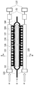
本実施形態のマッハツェンダ光変調器は、図9のマッハツェンダ光変調器のように別チップ部材の固定減衰器を設置するのでは無く、シリコンフォトニクス上にモノリシックに形成したダミー位相変調部53を設けた構成である。ダミー位相変調部53が、大きな減衰作用を持つ固定減衰器の役割を果たす。シリコンフォトニクス上にモノリシックに形成したダミー位相変調部53もまた、1対2本の並行する導波路(第1の導波路102及び第2の導波路103の光伝搬方向にある)と、位相変調部の光伝搬方向に向かって位相変調部よりも長く形成された進行波電極108とを備える。ダミー位相変調部53の1対2本の並行する導波路もまた、リブ導波路であり、第1の極性を持つ領域及び第2の極性を持つ領域に分かれている。第2の極性を持つ領域には、金属のバイアス電極54が設けられている。
ダミー位相変調部53の断面構造は、図3に示した位相変調部の断面構造と同じであるが、マッハツェンダ光変調器の出力部には接続されていない。一般的に、PN接合が装荷された進行波電極は高周波通過時の減衰特性が大きくなるために、固定減衰器として作用させることができる。
図9に示したマッハツェンダ光変調器と異なり、バルクの固定減衰器52を進行波電極108とパッド110の間に設置した構成ではないため、本実施形態のマッハツェンダ光変調器は、実装コストや部品点数を削減し低コスト化することができる。さらに、ダミー位相変調部53の第1の極性を持つ領域105及び第2の極性を持つ領域106のドーピング濃度を、位相変調部の第1の極性を持つ領域105及び第2の極性を持つ領域106のドーピング濃度よりも大きくすれば、ダミー位相変調部53に接続される進行波電極108の減衰量は大きくなり、小型化しつつ、リップル量を抑えることができる。
図1に示したように、シリコン変調器に位相変調部においては一般的に2種類以上のドーピング濃度を用いる。図10のダミー位相変調部53においては、光導波路コア20及びスラブ領域21を、高濃度p型半導体層(p++)および高濃度n型半導体層(n++)のみを用いたPN接合とすることで、より効率よく減衰作用を得ることができる。また、図8を参照して上述したように、ダミー位相変調部53における進行波電極108の幅、電極間隔を調整することで、位相変調部とダミー位相変調部の間のインピーダンスマッチングを整合させることができる。これによって、リップルのない信号品質の良い光を送信することができる。
図10においては、ダミー位相変調部53にバイアス電極54を設けた構成を示したが、バイアス電極54は無くとも良い。バイアス電極54がある場合には、バイアス電極54に逆バイアスする電圧を変化させることで、PN接合の空乏層を変化させ、ダミー位相変調部53における減衰量とインピーダンスを変化させることができる。一般的に、逆バイアスが大きければ空乏層は大きく開く為、キャパシタンス性が小さくなり、減衰量は減るが、インピーダンスは大きくなる。ダミー位相変調部53を設けた場合には、位相変調部とダミー位相変調部53との間のインピーダンスミスマッチにより、高周波の反射が生じ、リップルが生じうる。バイアス電極54を設けた場合には、前述の、位相変調部とダミー位相変調部との間のインピーダンスミスマッチによって生じうるリップルをバイアスによって調整しつつ、ダミー位相変調部53の減衰量も制御出来る為、変調器全体として最もリップルが低減するバイアスに調整することが出来る。
さらにこの効果は、マッハツェンダ光変調器を作製した後にダミー位相変調部53のインピーダンス特性がばらついた場合においても、インピーダンスを調整できるようになるため、変調器全体として、最もリップルが低減するように調整が可能となる。
(実施形態5)
図11は、本発明の第5の実施形態に係る光送信機を示す平面図である。本実施形態の光送信器は、図10を参照して説明した本発明の第4の実施形態に係るマッハツェンダ光変調器を用いた光送信機である。図4に示したマッハツェンダ光変調器の進行波電極108(出力側パッド110)を終端抵抗51を介して端子516(電源の電位)に接続する接続構成と異なり、図11の構成は、終端抵抗51を介さずに、図10のマッハツェンダ光変調器の進行波電極108を端子516(電源の電位)に接続することに特徴がある。図10のマッハツェンダ光変調器の代わりに、図8または9のマッハツェンダ光変調器を用いてもよい。
図11は、本発明の第5の実施形態に係る光送信機を示す平面図である。本実施形態の光送信器は、図10を参照して説明した本発明の第4の実施形態に係るマッハツェンダ光変調器を用いた光送信機である。図4に示したマッハツェンダ光変調器の進行波電極108(出力側パッド110)を終端抵抗51を介して端子516(電源の電位)に接続する接続構成と異なり、図11の構成は、終端抵抗51を介さずに、図10のマッハツェンダ光変調器の進行波電極108を端子516(電源の電位)に接続することに特徴がある。図10のマッハツェンダ光変調器の代わりに、図8または9のマッハツェンダ光変調器を用いてもよい。
一般的には、終端抵抗を用いない場合、Rout、Z、及びRterm(この場合は電源のインピーダンスに依存し、一般的に数Kohm)におけるインピーダンスミスマッチにより、光変調器の高周波特性が大きなリプルを持つことになる。
しかし、光送信器を構成するマッハツェンダ光変調器として、図8,9および10に示したマッハツェンダ光変調器のいずれかを用いることで、終端抵抗51を用いずに、端子516を介して接続される電源のインピーダンスと進行波電極108のインピーダンスにミスマッチがある場合にもリップル量を低減させることができる。したがって、終端抵抗51を用いない場合にもリップルを低減することができる為、光送信機の信号品質を犠牲にせずに、部品点数を削減し、低コスト化が可能となる。また、部品点数の削減により、光送信機の製品信頼性の向上と、実装による歩留り向上の効果も得られる。
1、3 SiO2クラッド層
2 Si層
7 光導波路
20 光導波路コア
21 スラブ領域
22 高濃度p型半導体層、
23 高濃度n型半導体層
24 中濃度p型半導体層
25 中濃度n型半導体層
101 入力光カプラ
102、103 導波路(リブ導波路)
104 出力光カプラ
105 第1の極性を持つ領域
106 第2の極性を持つ領域
54、107 バイアス電極
108 進行波電極
109、501、511 入力側パッド
110、504、513 出力側パッド
50 ドライバ
502、503 増幅回路
505、514 ワイヤ
51 終端抵抗
512 抵抗
516 端子(電位)
52 固定減衰器
53 ダミー位相変調部
2 Si層
7 光導波路
20 光導波路コア
21 スラブ領域
22 高濃度p型半導体層、
23 高濃度n型半導体層
24 中濃度p型半導体層
25 中濃度n型半導体層
101 入力光カプラ
102、103 導波路(リブ導波路)
104 出力光カプラ
105 第1の極性を持つ領域
106 第2の極性を持つ領域
54、107 バイアス電極
108 進行波電極
109、501、511 入力側パッド
110、504、513 出力側パッド
50 ドライバ
502、503 増幅回路
505、514 ワイヤ
51 終端抵抗
512 抵抗
516 端子(電位)
52 固定減衰器
53 ダミー位相変調部
Claims (4)
- 基板上に形成され、少なくともひとつの光入力と、少なくともひとつの光出力と、少なくともひとつの位相変調部を備えた光変調器であって、
前記位相変調部が、
PN接合構造を有する光導波路と、
変調用の高周波信号を印加して、前記光導波路を伝播する光が同一方向に伝搬しながら相互作用する進行波電極と
を備え、前記進行波電極が、前記位相変調部の光伝搬方向に、前記位相変調部よりも長く形成され、減衰領域を構成し、
前記減衰領域がダミー位相変調部であり、前記ダミー位相変調部が、
前記進行波電極の前記位相変調部よりも長く形成された部分と、
前記位相変調部の光導波路と同じPN接合構造を有し、前記位相変調部の光導波路と接続されない光導波路と
を備えた、光変調器。 - 前記ダミー位相変調部の光導波路のドーピング濃度が前記位相変調部の光導波路のドーピング濃度よりも高く、前記減衰領域を構成する前記進行波電極の前記位相変調部よりも長く形成された部分における前記高周波信号の損失が大きい、請求項1に記載の光変調器。
- 前記ダミー位相変調部が、バイアス電極をさらに備えた、請求項1または2に記載の光変調器。
- 請求項1乃至3のいずれか一項に記載の光変調器を備え、前記進行波電極の終端側に終端抵抗が接続されていない、光送信機。
Priority Applications (1)
| Application Number | Priority Date | Filing Date | Title |
|---|---|---|---|
| US17/429,268 US11841598B2 (en) | 2019-02-19 | 2020-02-07 | Optical modulator |
Applications Claiming Priority (2)
| Application Number | Priority Date | Filing Date | Title |
|---|---|---|---|
| JP2019027712A JP7131425B2 (ja) | 2019-02-19 | 2019-02-19 | 光変調器 |
| JP2019-027712 | 2019-02-19 |
Publications (1)
| Publication Number | Publication Date |
|---|---|
| WO2020170871A1 true WO2020170871A1 (ja) | 2020-08-27 |
Family
ID=72145106
Family Applications (1)
| Application Number | Title | Priority Date | Filing Date |
|---|---|---|---|
| PCT/JP2020/004954 Ceased WO2020170871A1 (ja) | 2019-02-19 | 2020-02-07 | 光変調器 |
Country Status (3)
| Country | Link |
|---|---|
| US (1) | US11841598B2 (ja) |
| JP (1) | JP7131425B2 (ja) |
| WO (1) | WO2020170871A1 (ja) |
Families Citing this family (4)
| Publication number | Priority date | Publication date | Assignee | Title |
|---|---|---|---|---|
| JP6927459B1 (ja) * | 2020-11-19 | 2021-09-01 | 三菱電機株式会社 | 光半導体素子、光制御装置 |
| WO2023032050A1 (ja) * | 2021-08-31 | 2023-03-09 | 住友大阪セメント株式会社 | 光導波路素子及びそれを用いた光変調デバイス並びに光送信装置 |
| CN114994958A (zh) * | 2022-05-31 | 2022-09-02 | 北京工业大学 | 一种基于铌酸锂薄膜波导的偏振无关双向调制器及调制方法 |
| CN119717166A (zh) * | 2023-09-28 | 2025-03-28 | 青岛海信宽带多媒体技术有限公司 | 一种光模块及混合InP/Si光芯片组件 |
Citations (6)
| Publication number | Priority date | Publication date | Assignee | Title |
|---|---|---|---|---|
| JP2003530592A (ja) * | 2000-04-06 | 2003-10-14 | ブッカム・テクノロジー・ピーエルシー | 予め決められた周波数チャープを有する光変調器 |
| JP2004102160A (ja) * | 2002-09-12 | 2004-04-02 | Fujitsu Quantum Devices Ltd | 光変調器及びその製造方法 |
| US20110135242A1 (en) * | 2009-12-08 | 2011-06-09 | Cogo Optronics, Inc. | Traveling wave mach-zehnder optical device |
| JP2011197427A (ja) * | 2010-03-19 | 2011-10-06 | Fujitsu Ltd | 半導体光変調器及びそれを用いた半導体光送信機 |
| JP2015148711A (ja) * | 2014-02-06 | 2015-08-20 | 日本電信電話株式会社 | 半導体マッハツェンダ光変調器 |
| WO2017159782A1 (ja) * | 2016-03-18 | 2017-09-21 | 日本電信電話株式会社 | 光変調器 |
Family Cites Families (9)
| Publication number | Priority date | Publication date | Assignee | Title |
|---|---|---|---|---|
| WO2013062096A1 (ja) * | 2011-10-26 | 2013-05-02 | 株式会社フジクラ | 光学素子及びマッハツェンダ型光導波路素子 |
| WO2014104309A1 (ja) * | 2012-12-27 | 2014-07-03 | 株式会社フジクラ | 光変調素子 |
| CA2969504C (en) * | 2014-12-09 | 2019-02-26 | Nippon Telegraph And Telephone Corporation | Optical modulator |
| SG11201800806WA (en) * | 2015-08-04 | 2018-02-27 | Nippon Telegraph & Telephone | Optical modulator |
| JP2018105975A (ja) * | 2016-12-26 | 2018-07-05 | 株式会社フジクラ | 光変調素子 |
| US11460724B2 (en) * | 2017-04-28 | 2022-10-04 | Ciena Corporation | Optical modulator robust to fabrication errors through an RF electrical crossing |
| JP7056247B2 (ja) * | 2018-03-08 | 2022-04-19 | 富士通オプティカルコンポーネンツ株式会社 | 光送受信デバイスおよび光送受信モジュール |
| JP6823619B2 (ja) * | 2018-04-19 | 2021-02-03 | 日本電信電話株式会社 | 光変調器 |
| JP7095583B2 (ja) * | 2018-12-11 | 2022-07-05 | 日本電信電話株式会社 | 光送信機 |
-
2019
- 2019-02-19 JP JP2019027712A patent/JP7131425B2/ja active Active
-
2020
- 2020-02-07 US US17/429,268 patent/US11841598B2/en active Active
- 2020-02-07 WO PCT/JP2020/004954 patent/WO2020170871A1/ja not_active Ceased
Patent Citations (6)
| Publication number | Priority date | Publication date | Assignee | Title |
|---|---|---|---|---|
| JP2003530592A (ja) * | 2000-04-06 | 2003-10-14 | ブッカム・テクノロジー・ピーエルシー | 予め決められた周波数チャープを有する光変調器 |
| JP2004102160A (ja) * | 2002-09-12 | 2004-04-02 | Fujitsu Quantum Devices Ltd | 光変調器及びその製造方法 |
| US20110135242A1 (en) * | 2009-12-08 | 2011-06-09 | Cogo Optronics, Inc. | Traveling wave mach-zehnder optical device |
| JP2011197427A (ja) * | 2010-03-19 | 2011-10-06 | Fujitsu Ltd | 半導体光変調器及びそれを用いた半導体光送信機 |
| JP2015148711A (ja) * | 2014-02-06 | 2015-08-20 | 日本電信電話株式会社 | 半導体マッハツェンダ光変調器 |
| WO2017159782A1 (ja) * | 2016-03-18 | 2017-09-21 | 日本電信電話株式会社 | 光変調器 |
Non-Patent Citations (1)
| Title |
|---|
| WOLF, N. ET AL.: "Electro-Optical Co-Design to Minimize Power Consumption of a 32 GBd Optical IQ - Transmitter Using InP MZ-Modulators", IEEE COMPOUND SEMICONDUCTOR INTEGRATED CIRCUIT SYMPOSIUM (CSICS, 11 October 2015 (2015-10-11), pages 1 - 4, XP032804746, Retrieved from the Internet <URL:https://ieeexplore.ieee.org/document/7314499> DOI: 10.1109/CSICS.2015.7314499 * |
Also Published As
| Publication number | Publication date |
|---|---|
| JP2020134689A (ja) | 2020-08-31 |
| US11841598B2 (en) | 2023-12-12 |
| US20220137478A1 (en) | 2022-05-05 |
| JP7131425B2 (ja) | 2022-09-06 |
Similar Documents
| Publication | Publication Date | Title |
|---|---|---|
| US9448425B2 (en) | Optical waveguide element and optical modulator | |
| CN101485055B (zh) | 具有集成调制器阵列和混合键合的多波长激光器阵列的发射器-接收器 | |
| JP6434991B2 (ja) | 光変調器 | |
| US11841598B2 (en) | Optical modulator | |
| WO2018174083A1 (ja) | Iq光変調器 | |
| JP7196736B2 (ja) | 光導波路素子、及び光導波路デバイス | |
| JPWO2019106890A1 (ja) | 半導体光変調器 | |
| JP3885528B2 (ja) | 光変調器 | |
| JP7453585B2 (ja) | 半導体光変調器 | |
| JP6734813B2 (ja) | 光送信機 | |
| JP7139965B2 (ja) | 半導体マッハツェンダ光変調器 | |
| US6763151B1 (en) | Electro-optic modulators with internal impedance matching | |
| CN110573940A (zh) | 半导体马赫-曾德尔型光调制器 | |
| JP2018097093A (ja) | 光変調器 | |
| JP6823619B2 (ja) | 光変調器 | |
| JP2017173365A (ja) | 光変調器 | |
| JP2022047597A (ja) | 光デバイスおよび光送受信機 | |
| JP6431493B2 (ja) | 光変調器 | |
| US20250264772A1 (en) | Optical waveguide modulator | |
| US20250264744A1 (en) | Optical modulation device, optical modulator, optical modulation module, optical transmission apparatus, and optical transmission system | |
| US20250264746A1 (en) | Optical modulation device, optical modulator, optical modulation module, optical transmission apparatus, and optical transmission system | |
| US20250264745A1 (en) | Optical modulation device, optical modulator, optical modulation module, optical transmission apparatus, and optical transmission system | |
| US11320715B2 (en) | Optical device that includes optical modulator | |
| WO2023095261A1 (ja) | マッハツェンダ変調器 | |
| WO2023248489A1 (ja) | 光変調器 |
Legal Events
| Date | Code | Title | Description |
|---|---|---|---|
| 121 | Ep: the epo has been informed by wipo that ep was designated in this application |
Ref document number: 20759010 Country of ref document: EP Kind code of ref document: A1 |
|
| NENP | Non-entry into the national phase |
Ref country code: DE |
|
| 122 | Ep: pct application non-entry in european phase |
Ref document number: 20759010 Country of ref document: EP Kind code of ref document: A1 |