WO2020170801A1 - 光学部材、光学部材の製造方法及び光情報伝達装置 - Google Patents
光学部材、光学部材の製造方法及び光情報伝達装置 Download PDFInfo
- Publication number
- WO2020170801A1 WO2020170801A1 PCT/JP2020/004094 JP2020004094W WO2020170801A1 WO 2020170801 A1 WO2020170801 A1 WO 2020170801A1 JP 2020004094 W JP2020004094 W JP 2020004094W WO 2020170801 A1 WO2020170801 A1 WO 2020170801A1
- Authority
- WO
- WIPO (PCT)
- Prior art keywords
- optical
- optical member
- flatness
- polishing
- resin
- Prior art date
- Legal status (The legal status is an assumption and is not a legal conclusion. Google has not performed a legal analysis and makes no representation as to the accuracy of the status listed.)
- Ceased
Links
Images
Classifications
-
- G—PHYSICS
- G02—OPTICS
- G02B—OPTICAL ELEMENTS, SYSTEMS OR APPARATUS
- G02B1/00—Optical elements characterised by the material of which they are made; Optical coatings for optical elements
- G02B1/04—Optical elements characterised by the material of which they are made; Optical coatings for optical elements made of organic materials, e.g. plastics
-
- B—PERFORMING OPERATIONS; TRANSPORTING
- B24—GRINDING; POLISHING
- B24B—MACHINES, DEVICES, OR PROCESSES FOR GRINDING OR POLISHING; DRESSING OR CONDITIONING OF ABRADING SURFACES; FEEDING OF GRINDING, POLISHING, OR LAPPING AGENTS
- B24B37/00—Lapping machines or devices; Accessories
- B24B37/04—Lapping machines or devices; Accessories designed for working plane surfaces
- B24B37/07—Lapping machines or devices; Accessories designed for working plane surfaces characterised by the movement of the work or lapping tool
- B24B37/08—Lapping machines or devices; Accessories designed for working plane surfaces characterised by the movement of the work or lapping tool for double side lapping
-
- G—PHYSICS
- G02—OPTICS
- G02B—OPTICAL ELEMENTS, SYSTEMS OR APPARATUS
- G02B27/00—Optical systems or apparatus not provided for by any of the groups G02B1/00 - G02B26/00, G02B30/00
- G02B27/01—Head-up displays
- G02B27/0101—Head-up displays characterised by optical features
- G02B2027/0123—Head-up displays characterised by optical features comprising devices increasing the field of view
- G02B2027/0125—Field-of-view increase by wavefront division
-
- G—PHYSICS
- G02—OPTICS
- G02B—OPTICAL ELEMENTS, SYSTEMS OR APPARATUS
- G02B27/00—Optical systems or apparatus not provided for by any of the groups G02B1/00 - G02B26/00, G02B30/00
- G02B27/01—Head-up displays
- G02B27/017—Head mounted
- G02B27/0172—Head mounted characterised by optical features
-
- G—PHYSICS
- G02—OPTICS
- G02B—OPTICAL ELEMENTS, SYSTEMS OR APPARATUS
- G02B6/00—Light guides; Structural details of arrangements comprising light guides and other optical elements, e.g. couplings
- G02B6/24—Coupling light guides
- G02B6/26—Optical coupling means
- G02B6/262—Optical details of coupling light into, or out of, or between fibre ends, e.g. special fibre end shapes or associated optical elements
Definitions
- the present disclosure relates to an optical member, a method for manufacturing the optical member, and an optical information transmission device.
- glass substrates for electronic devices In recent years, demands for flatness, surface defects, etc. of glass substrates for electronic devices have become strict, and for example, glass substrates for mask blanks having high flatness and few minute defects (concave defects, convex defects), etc. Glass substrates for electronic devices are required.
- a polishing pad As a method of manufacturing a glass substrate for a mask blank having such a high flatness and a small number of micro defects (concave defects, convex defects), a polishing pad is attached and an upper surface plate provided vertically opposite to each other.
- Patent Document 1 Japanese Patent No. 6002528
- the optical members can transmit light with high precision, and inorganic materials such as glass have been used because they are easy to manufacture by polishing.
- wearable optical members have been required to be lightweight, and the optical members made of an inorganic material have been thinned to reduce the weight.
- the problems of the present disclosure have been made in view of the above problems, are lightweight, and are capable of accurately transmitting optical information, an optical member and a manufacturing method thereof, and an optical information transmission device including the optical member. Is to provide.
- the present disclosure relates to the following aspects.
- ⁇ 1> Including an organic polymer, An optical member including a surface A having an area of 1 mm 2 or more and having a flatness of 80 ⁇ m or less when the flatness of a region having an area of 1 mm 2 is measured by a non-contact optical flatness meter.
- ⁇ 2> The optical member according to ⁇ 1>, wherein the flatness of the surface A is 50 ⁇ m or less.
- ⁇ 3> A surface B located on the opposite side of the surface A and having an area of 1 mm 2 or more, When the flatness of the area of 1 mm 2 is measured for each of the surfaces A and B with a non-contact optical flatness meter, the absolute value of the difference between the flatness of the surface A and the flatness of the surface B is The optical member according to ⁇ 1> or ⁇ 2>, which has a thickness of 5 ⁇ m or less.
- Area includes a surface A is 1 mm 2 or more, located on the opposite side of the surface A, surface B area is 1 mm 2 or more, When the flatness of the area of 1 mm 2 is measured for each of the surfaces A and B with a non-contact optical flatness meter, the absolute value of the difference between the flatness of the surface A and the flatness of the surface B is An optical member having a thickness of 5 ⁇ m or less.
- ⁇ 5> The optical member according to ⁇ 3> or ⁇ 4>, wherein an average distance between the surface A and the surface B is 10 mm or less.
- the arithmetic mean roughness Ra of the surface A is 10 nm or less when the arithmetic mean roughness Ra of the area of 4200 ⁇ m 2 is measured by a non-contact optical surface roughness meter.
- the optical member according to any one of claims. ⁇ 7> The optical member according to any one of ⁇ 1> to ⁇ 6>, which has a refractive index of 1.58 or more. ⁇ 8> When a region having an area of 4200 ⁇ m 2 is imaged by a non-contact optical surface roughness meter, a plurality of linear parts with a height of 50 nm or less are observed in the image of the surface A.
- ⁇ 1> to ⁇ 7> The optical member according to any one of claims.
- ⁇ 9> The optical member according to any one of ⁇ 1> to ⁇ 8>, which has a Vickers hardness at 23° C. of 1 GPa or less.
- ⁇ 10> The optical member according to any one of ⁇ 1> to ⁇ 9>, which has a tensile elastic modulus at 23° C. of 1.0 ⁇ 10 3 MPa to 5.0 ⁇ 10 3 MPa.
- the organic polymer is a poly(thio)urethane resin, episulfide resin, polycarbonate resin, polyester resin, polyamide resin, polyimide resin, poly(meth)acrylate resin, polyolefin resin, polyureaurethane resin, polysulfide resin, poly( The optical member according to any one of ⁇ 1> to ⁇ 10>, containing at least one selected from the group consisting of a (meth)(thio)acrylate resin and an allyldiglycidyl carbonate resin.
- ⁇ 13> A method for manufacturing the optical member according to any one of ⁇ 1> to ⁇ 12>, A step of preparing a molded member containing an organic polymer, Including a first polishing step of polishing the molding member with a polishing pad after disposing the molding member in a movement restricting portion that regulates the movement of the molding member when polishing the molding member, In the first polishing step, a method for manufacturing an optical member, in which the molded member is polished with an abrasive having a particle size of 3 ⁇ m or more.
- ⁇ 14> The method for manufacturing an optical member according to ⁇ 13>, wherein the molding member is movable relative to the movement restricting portion when the molding member is polished by the polishing pad.
- ⁇ 15> The method for manufacturing an optical member according to ⁇ 13> or ⁇ 14>, wherein in the first polishing step, the molding member is arranged in the movement restricting portion so that the clearance is 1 mm or more.
- ⁇ 16> The optical member according to any one of ⁇ 13> to ⁇ 15>, further including a second polishing step of polishing the molded member after performing the first polishing step with a polishing pad and an abrasive. Production method.
- An optical information transmission device comprising:
- an optical member that is lightweight and capable of transmitting optical information with high precision, a method for manufacturing the optical member, and an optical information transmission device including the optical member.
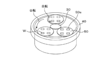
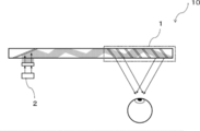
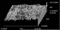
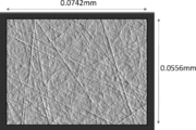
- FIG. 6 is a perspective view showing a meshing relationship between a sun gear, an internal gear, and a movement restricting unit in a planetary gear system. It is a schematic structure figure showing an example of an optical information transmission device of this indication. It is three-dimensional data imaged by a non-contact optical surface roughness meter. This is image data of polishing marks.
- optical member refers to a member including at least one layer of an organic polymer.
- the optical member of the present disclosure may be in the form of a laminated body in which a plurality of members containing an organic polymer are laminated, or in the form of a laminated body in which other members are laminated.
- the optical member of the present disclosure includes an organic polymer, has an area of 1 mm 2 or more, and has a flatness of 80 ⁇ m or less when the flatness of a region having an area of 1 mm 2 is measured by a non-contact optical flatness meter. Includes surface A.
- the optical member of the present disclosure is lightweight because it is configured to include an organic polymer, and further includes the surface A having a flatness of 80 ⁇ m or less, so that optical information can be accurately transmitted.
- the position of the surface A in the optical member of the present disclosure is not particularly limited, and a configuration in which the surface A is located on at least a part of the exposed surface (including the main surface) of the optical member has a high flatness of the surface A. It is preferable because optical information can be easily transmitted depending on the degree.
- the surface A is located on a part of the exposed surface of the optical member of the present disclosure, it is preferable that the surface A is located at a place where the optical information transmitted by the surface A is easily received.
- the area including the main surface of the optical member and the center of gravity of the main surface is preferable.
- the area measured by the non-contact optical flatness meter is not particularly limited as long as the area of the surface A is 1 mm 2 . Therefore, the surface A in the optical member of the present disclosure may have a region having an area of 1 mm 2 having a flatness of 80 ⁇ m or less, and the other regions of the surface A may have a flatness of 80 ⁇ m or less, It may be more than 80 ⁇ m.
- the flatness of the entire surface A may be 80 ⁇ m or less, 10% or more of the total area of the surface A, preferably 50% or more of the total area of the surface A, and the flatness of 80 ⁇ m or less. Good.
- the area measured by the non-contact optical flatness meter may be an area having an area centered on the center of gravity of the surface A of 1 mm 2 .
- the flatness of the surface A may be 80 ⁇ m or less, and is preferably 50 ⁇ m or less, more preferably 30 ⁇ m or less, further preferably 20 ⁇ m or less, and 15 ⁇ m or less from the viewpoint of transmitting optical information. It is particularly preferable that The lower limit of the flatness of the surface A is not particularly limited as long as it is 0 ⁇ m or more, and may be 1 ⁇ m or more or 5 ⁇ m or more.
- the area of the surface A may be 1 mm 2 or more and is appropriately determined according to the application of the optical member.
- the area of the surface A may be 10 mm 2 to 20000 mm 2 , or 100 mm 2 to 1000 mm 2 .
- the optical member of the present disclosure may include a surface B located on the opposite side of the surface A and having an area of 1 mm 2 or more.
- the preferable range of the area of the surface B is the same as the preferable range of the area of the surface A. Further, the areas of the surface A and the surface B may be the same or different.
- the flatness of the surface B in the area of 1 mm 2 is measured by a non-contact optical flatness meter, the flatness may be 80 ⁇ m or less.
- the preferable range of the flatness of the surface B is the same as the preferable range of the flatness of the surface A described above.
- the optical member of the present disclosure can transmit optical information with higher accuracy.
- a plurality of the optical members of the present disclosure are laminated so that the regions having a parallelism of 5 ⁇ m or less are in contact with each other to form a laminated structure. In such a case, it becomes possible to accurately transmit optical information in the laminated structure.
- the above parallelism is more preferably 4 ⁇ m or less, further preferably 3 ⁇ m or less.
- the lower limit of parallelism is not particularly limited as long as it is 0 ⁇ m or more, and may be 0.5 ⁇ m or more, or 1.0 ⁇ m or more.
- the average distance between the surfaces A and B may be 10 mm or less, 8 mm or less, or 6 mm or less.
- the average distance between the surfaces A and B may be 2 mm or more, or 4 mm or more.
- “the average of the distances between the surfaces A and B” is a value obtained by dividing the sum of the maximum distance between the surfaces A and B and the minimum distance between the surfaces A and B by 2. means.
- the arithmetic average roughness Ra of the surface A when the arithmetic average roughness Ra of the area of 4200 ⁇ m 2 is measured by a non-contact optical surface roughness meter is preferably 10 nm or less, and more preferably 5 nm or less. preferable. Further, the arithmetic mean roughness Ra of the surface A may be more than 0.1 nm.
- the arithmetic mean roughness Ra of the present disclosure is based on JIS B0601 (2013).
- the area measured by the non-contact optical surface roughness meter is not particularly limited as long as the area of the surface A is 4200 ⁇ m 2 . Therefore, the surface A in the optical member of the present disclosure only needs to have a region having an area of 4200 ⁇ m 2 where the arithmetic average roughness Ra is 10 nm or less, and the other regions of the surface A have an arithmetic average roughness Ra of 10 nm or less. Or may be more than 10 nm.
- the optical member of the present disclosure when a region having an area of 4200 ⁇ m 2 is imaged by a non-contact optical surface roughness meter, it is preferable that a plurality of linear portions having a height of 50 nm or less are observed in the image of the surface A. Accordingly, for example, when a plurality of optical members of the present disclosure are stacked so that the regions where the linear portions are observed are in contact with each other, the stacked structure can be easily held.
- the plurality of linear portions described above may be polishing marks, or may be polishing marks formed by polishing a molded member by a manufacturing method described later. As an example, FIG.
- FIG. 3 shows three-dimensional data of the optical member of the present disclosure which is imaged by a non-contact optical surface roughness meter
- FIG. 4 shows image data of polishing marks in the optical member of the present disclosure.
- At least a part of the plurality of linear parts may be arranged in parallel or may intersect.
- the surface A and other layers for example, an adhesive layer and a pressure-sensitive adhesive layer
- the surface A and other members are laminated, because at least some of the plurality of linear portions intersect.
- the area measured and observed by the non-contact optical surface roughness meter may be an area whose area centered on the center of gravity of the surface A is 4200 ⁇ m 2 .
- the adhesiveness with the other layer is increased, so that the surface A and the other layer are positioned. It becomes difficult to shift. Further, when another member is installed so as to come into contact with the surface A, the surface A and the other member are less likely to be displaced in position.
- the Vickers hardness at 23° C. of the optical member of the present disclosure is preferably 1 GPa or less. That is, a relatively soft optical member is preferable.
- the Vickers hardness at 23° C. of the optical member may be measured according to JIS Z 2244 (2009).
- the tensile modulus at 23° C. of the optical member of the present disclosure is preferably 1.0 ⁇ 10 3 MPa to 5.0 ⁇ 10 3 MPa.
- the tensile elastic modulus at 23° C. of the optical member may be measured according to JIS K 7161-1 (2014).
- an optical member having at least one of the Vickers hardness at 23° C. and the tensile elastic modulus at 23° C. described above and having excellent surface A flatness can be obtained by the method for producing an optical member of the present disclosure described later.
- the total light transmittance of the optical member may be 10% or more.
- the total light transmittance of the optical member may be measured according to JIS K 7361-1 (1997).
- the haze (total haze) of the optical member is preferably 10% or less, more preferably 1% or less, still more preferably 0.5% or less.
- the haze of the optical member is a value measured at 25° C. in accordance with JIS-K7105 using a haze measuring machine [TC-HIII DPK manufactured by Tokyo Denshoku Co., Ltd.].
- the shape of the optical member is not particularly limited, and may be a plate shape, a cylindrical shape, a rectangular parallelepiped shape, or the like.
- the optical member is processed to adjust the shape, if the optical member is processed after forming the surface A of the optical member, the parallelism, flatness, and the like of the surface A are likely to be impaired. It is preferable to process the member.
- the shape of the optical member is a shape having a corner such as a plate shape or a rectangular parallelepiped shape
- the shape of the optical member is a shape having a corner such as a plate shape or a rectangular parallelepiped shape
- the shape of the optical member is a shape having a corner such as a plate shape or a rectangular parallelepiped shape
- the shape of the optical member is a shape having a corner such as a plate shape or a rectangular parallelepiped shape
- the force for forming the surface A is concentrated on the corner, and the parallelism around the corner is increased.
- the flatness is
- the surface A when forming the surface A, the surface A can be formed without applying excessive force to the corners, and the parallelism, flatness, etc. of the optical member can be obtained. The value of can be lowered.
- the refractive index of the optical member is preferably 1.58 or more.
- the refractive index of the optical member may be 1.80 or less, or 1.75 or less.
- the refractive index of the optical member may be measured according to JIS K7142 (2014).
- the organic polymer contained in the optical member includes poly(thio)urethane resin, episulfide resin, polycarbonate resin, polyester resin, polyamide resin, polyimide resin, poly(meth)acrylate resin, polyolefin resin, polyureaurethane resin, polysulfide resin, It preferably contains at least one selected from the group consisting of poly(meth)(thio)acrylate resins and allyldiglycidyl carbonate resins.
- poly(thio)urethane resin, episulfide resin and polycarbonate resin are preferable, and poly(thio)urethane resin and episulfide resin are more preferable, from the viewpoint of refractive index.
- a thiourethane resin is preferable, and more specifically, a thiourethane resin obtained by polymerizing a diisocyanate compound and a thiol compound is preferable.
- diisocyanate compound examples include 2,4-tolylene diisocyanate, 2,6-tolylene diisocyanate, diphenylmethane diisocyanate, m-xylylene diisocyanate, m-phenylene diisocyanate, isophorone diisocyanate, hexamethylene diisocyanate and 2,5-bis(isocyanato).
- the diisocyanate compound may be used alone or in combination of two or more kinds.
- thiol compounds include pentaerythritol tetrakis (3-mercaptopropionate), pentaerythritol tetrakis (2-mercaptoacetate), 4-mercaptomethyl-1,8-dimercapto-3,6-dithiaoctane, 5,7-dimercapto.
- the thiol compounds may be used alone or in combination of two or more.
- the episulfide resin may be any one that uses a compound having an episulfide group as the main component or subcomponent of the starting material of the resin, and examples of the compound having an episulfide group include WO 2017/159839, Examples thereof include episulfide compounds described in JP-A-2018-154690, thioepoxy compounds described in JP-A-2002-194083, and novel tetrathiaspiro compounds described in JP-A-2019-1785.
- the content of the organic polymer contained in the optical member is preferably 80% by mass or more, and more preferably 90% by mass or more based on the total amount of the optical member.
- the content of the organic polymer contained in the optical member may be 100% by mass or 99% by mass or less based on the total amount of the optical member.
- the optical member may contain other components in addition to the organic polymer.
- other components include ultraviolet absorbers, antioxidants, light stabilizers, deterioration inhibitors, dyes (photochromic materials, etc.), release agents, dyes, pigments, polymerization catalysts, and the like.
- the optical member of the present disclosure is not particularly limited and can be used in, for example, a display device, an imaging device, an optical device, and the like.
- the optical member can be used more specifically in a wearable device, and more specifically, can be used in a wearable display that realizes virtual reality (VR), augmented reality (AR), or the like. be able to.
- VR virtual reality
- AR augmented reality
- the method for producing an optical member according to the present disclosure includes a step of preparing a molded member containing an organic polymer (preparing step), and a movement restricting portion that restricts movement of the molded member when polishing the molded member. After arranging, the first polishing step of polishing the molded member with a polishing pad is included. In the first polishing step, the molded member is polished using an abrasive having a grain size of 3 ⁇ m or more. Thereby, the above-mentioned optical member of the present disclosure can be obtained.
- the manufacturing method of the present disclosure includes a step of preparing a molded member containing an organic polymer.
- the molding member is an optical member before the polishing treatment, and the shape of the molding member may be appropriately selected according to the shape of the optical member to be manufactured.
- a molding member may be formed by injecting a composition containing a monomer that is a raw material of an organic polymer into a molding die, and then irradiating the composition with ultraviolet rays or the like to polymerize the monomer.
- the manufacturing method of the present disclosure includes a first polishing step of polishing the molded member with a polishing pad after disposing the molded member in a movement restricting portion that restricts the movement of the molded member when polishing the molded member.
- the first polishing step at least one surface of the molded member, which is the surface A of the optical member, is polished, and preferably both surfaces of the optical member, which are the surfaces A and B, are polished.
- a single-sided polishing machine in which a polishing pad is installed on one of the upper and lower platens may be used.
- polishing pad on the upper and lower platens may be used.
- a double-sided polishing machine in which each is installed may be used.
- the movement restricting unit may have a configuration in which the molding member is arranged when the molding member is polished by the polishing pad and the movement of the molding member is regulated.
- the movement restricting portion may be configured to hold the molding member such that the molding member does not move relative to the movement restricting portion when the molding member is polished by the polishing pad.
- the molding member may be arranged so as to be movable relative to each other. In the latter configuration, an optical member having high flatness of the surface A and excellent parallelism of the surfaces A and B tends to be easily obtained.
- the molded member may be polished while supplying a known polishing liquid, grinding liquid, or the like.
- the first polishing step it is preferable to polish the molded member with an abrasive having a particle size of 5 ⁇ m to 10 ⁇ m from the viewpoint of the abradability of the molded member, and to polish the molded member with an abrasive having a particle size of 7 ⁇ m to 10 ⁇ m. More preferably.
- a polishing pad pad having a grain size of 3 ⁇ m or more
- an abrasive fixed abrasive
- a polishing member is used to polish the molded member using an abrasive material (free abrasive grains) such as diamond having a grain size of 3 ⁇ m or more.
- an abrasive material free abrasive grains
- the abrasive has a small particle size.
- the present inventors when polishing a molded member containing an organic polymer that is softer than an inorganic material, is different from usual, and by using an abrasive having a certain grain size or more, parallelism, flatness, and other values can be obtained. I found that I can lower.
- the molding member in the movement restricting portion so that the clearance is 1 mm or more. Thereby, an optical member having higher flatness of the surface A and more excellent parallelism of the surfaces A and B tends to be easily obtained.
- the above-mentioned clearance is preferably 3 mm or more, more preferably 5 mm or more, and further preferably 10 mm or more. Further, the clearance may be 30 mm or less.
- the “clearance” means that the maximum value of the distance between the side surfaces is the length A when the side surface of the movement restricting portion is polygonal, and the diameter when the side surface of the movement restricting portion is circular. Is the length A, and the maximum value of the distance between the side surfaces is B when the side surfaces of the forming member are polygonal, and the diameter B is the length B when the side surfaces of the forming member are circular. Means (AB)/2.
- the movement restricting portion and the peripheral portion of the molding member easily collide when the surface A is formed.
- the movement restricting portion and the peripheral edge of the molding member are caused. It is presumed that the parts are unlikely to be deformed even if they collide when the surface A is formed.
- the force applied to the inorganic molding member from the movement restricting portion easily propagates to the entire inorganic molding member, although it is considered that the parallelism, the flatness, and the like can be lowered, it is expected that the movement restricting portion and the peripheral edge of the inorganic molding member collide with each other and the inorganic molding member is easily damaged.
- the molded member may be polished by planetary polishing.
- the planetary polishing refers to polishing the molding member while revolving and rotating the movement restricting portion in which the molding member is arranged.
- FIG. 1 is a perspective view showing a meshing relationship between a sun gear, an internal gear, and a movement restricting portion in a planetary gear system.
- the sun gear 30 and the internal gear 40 arranged concentrically outside the sun gear 30 mesh with the sun gear 30 and the internal gear 40, depending on the rotation of the sun gear 30 and the internal gear 40.
- a movement restricting portion 50 that revolves around the sun and is rotated, and a plurality of forming members W are arranged in the movement restricting portion 50.
- the polishing pads installed on the upper and lower surface plates of the planetary gear type double-side polishing machine polishes both sides of the molding member W arranged in the movement restricting section 50.
- the rotation speed of the upper polishing pad is preferably 5 rpm to 30 rpm, more preferably 7 rpm to 20 rpm.
- the rotation speed of the lower polishing pad is preferably 20 rpm to 50 rpm, more preferably 25 rpm to 40 rpm.
- the upper polishing pad and the lower polishing pad may rotate in the same direction or in opposite directions.
- the orbital speed of the movement restricting portion in which the molding member is arranged is preferably 5 rpm to 30 rpm, more preferably 7 rpm to 20 rpm.
- the orbital direction of the movement restricting portion may be the same as or opposite to that of the lower polishing pad.
- the rotation speed of the movement restricting portion in which the molding member is arranged is preferably 2 rpm to 50 rpm, more preferably 5 rpm to 20 rpm.
- the method for manufacturing an optical member of the present disclosure further includes a second polishing step of polishing the molded member after performing the first polishing step with a polishing pad and an abrasive.
- a polishing pad different from that in the first polishing step for example, a suede type polishing pad in which a nap layer made of a resin such as urethane resin or ester resin is provided on a base material may be used. Good.
- the molded member may be polished while supplying a known polishing liquid, a polishing liquid, etc. containing a polishing material such as alumina.
- An optical information transmission device of the present disclosure includes a light irradiation unit and a plurality of the optical members of the present disclosure described above, and a light guide path in which the plurality of optical members are arranged so that main surfaces of the optical members are substantially parallel to each other. , Is provided. Since this optical information transmission device includes a plurality of the above-mentioned optical members, it is lightweight and capable of transmitting optical information with high accuracy.
- the above-described optical member of the present disclosure may be directly laminated, or may be laminated via an adhesive layer.
- the adhesive layer for example, a composition containing a monomer that is a raw material of an organic polymer is applied to an optical member to form a composition layer, and the formed composition layer is sandwiched between two optical members to form a composition. It may be formed by irradiating the layer with ultraviolet rays or the like to polymerize the monomer.
- the optical information transmission device 10 includes an image display unit 1 And a light guide path on which a plurality of optical members 2 are arranged.
- the light generated from the image display unit 1 is reflected by the optical member 2 of the light guide path, and the light reflected and spread by the plurality of optical members 2 is radiated to the eyes to be displayed on the image display unit 1.
- the displayed image is recognized by the user wearing the optical information transmission device 10.
- a disk-shaped molding member having a diameter of 80 mm and a height of 1.7 mm was prepared from the following materials.
- the Vickers hardness of the molded member was 228 MPa, and the tensile modulus of elasticity of the molded member at 23° C. was 3.8 ⁇ 10 3 MPa.
- MR10 thiourethane resin, refractive index 1.67, Mitsui Chemicals, Inc.
- the prepared molded member was placed on a fixing device (corresponding to a movement restricting portion) having openings on both sides of a polishing device (9B double-sided lapping machine) so that two circular surfaces would be surfaces to be polished.
- the clearance between the wall surface of the fixture and the molded member was 20 mm.
- the 1st polishing process was performed on the following polishing conditions using the polishing pad and grinding liquid shown below.
- the second polishing step was performed under the following polishing conditions using the polishing pad and the grinding liquid described below.
- the clearance between the wall surface of the fixture and the molded member was 20 mm.
- Polishing condition of the second polishing step Polishing the molded member by pouring the grinding fluid under the following conditions, rotating the upper pad and the lower pad under the following condition, and rotating and revolving the fixture with the molded member under the following conditions.
- a disk-shaped optical member having a diameter of 80 mm and a height of 0.81 mm was obtained by the first and second polishing steps described above.
- the second polishing step was performed in the same manner as in Experimental Examples 1 to 4 except that the rotation speed of the fixing device was changed from 5 rpm to 2 rpm and the revolution speed of the fixing device was changed from 10 rpm to 5 rpm.
- the polishing amount in the second polishing step was 22 ⁇ m.
- Example 8 The first polishing step was performed in the same manner as in Experimental Examples 1 to 4 except that the diamond tiles (pad mesh 9 ⁇ m, #2000 equivalent) in Experiment Examples 1 to 4 were changed to diamond tiles (pad mesh 2 ⁇ m, #6000 equivalent). It was However, in Experimental Example 8, the polishing of the molded member did not proceed.
- Example 9 The first polishing step was performed in the same manner as in Experimental Examples 5 to 7, except that the diamond tiles (pad mesh 9 ⁇ m, #2000 equivalent) in Experiment Examples 5 to 7 were changed to diamond tiles (pad mesh 2 ⁇ m, #6000 equivalent). It was However, in Experimental Example 9, the polishing of the molded member did not proceed.
Landscapes
- Physics & Mathematics (AREA)
- General Physics & Mathematics (AREA)
- Optics & Photonics (AREA)
- Engineering & Computer Science (AREA)
- Mechanical Engineering (AREA)
- Finish Polishing, Edge Sharpening, And Grinding By Specific Grinding Devices (AREA)
- Optical Elements Other Than Lenses (AREA)
Priority Applications (4)
| Application Number | Priority Date | Filing Date | Title |
|---|---|---|---|
| JP2021501822A JP7292689B2 (ja) | 2019-02-18 | 2020-02-04 | 光学部材、光学部材の製造方法及び光情報伝達装置 |
| CN202080010111.4A CN113330336B (zh) | 2019-02-18 | 2020-02-04 | 光学构件、光学构件的制造方法及光信息传递装置 |
| EP20758557.1A EP3910386A4 (en) | 2019-02-18 | 2020-02-04 | Optical member, method for manufacturing optical member, and optical information transmission device |
| US17/425,761 US11988807B2 (en) | 2019-02-18 | 2020-02-04 | Optical member, method of producing optical member, and apparatus for transmitting optical information |
Applications Claiming Priority (2)
| Application Number | Priority Date | Filing Date | Title |
|---|---|---|---|
| JP2019-026906 | 2019-02-18 | ||
| JP2019026906 | 2019-02-18 |
Publications (1)
| Publication Number | Publication Date |
|---|---|
| WO2020170801A1 true WO2020170801A1 (ja) | 2020-08-27 |
Family
ID=72144671
Family Applications (1)
| Application Number | Title | Priority Date | Filing Date |
|---|---|---|---|
| PCT/JP2020/004094 Ceased WO2020170801A1 (ja) | 2019-02-18 | 2020-02-04 | 光学部材、光学部材の製造方法及び光情報伝達装置 |
Country Status (5)
| Country | Link |
|---|---|
| US (1) | US11988807B2 (enExample) |
| EP (1) | EP3910386A4 (enExample) |
| JP (1) | JP7292689B2 (enExample) |
| CN (1) | CN113330336B (enExample) |
| WO (1) | WO2020170801A1 (enExample) |
Cited By (4)
| Publication number | Priority date | Publication date | Assignee | Title |
|---|---|---|---|---|
| WO2025018342A1 (ja) * | 2023-07-20 | 2025-01-23 | 三井化学株式会社 | 光学積層体、光学積層体の製造方法および光情報伝達装置 |
| WO2025018344A1 (ja) * | 2023-07-20 | 2025-01-23 | 三井化学株式会社 | 光学積層体、光学積層体の製造方法および光情報伝達装置 |
| WO2025143116A1 (ja) * | 2023-12-27 | 2025-07-03 | 三井化学株式会社 | 光学樹脂ウェハの製造方法 |
| WO2025164783A1 (ja) * | 2024-02-01 | 2025-08-07 | ホヤ レンズ タイランド リミテッド | 樹脂基板、導光板、導波路装置、アイウェア用光学部材及びウェアラブルデバイス |
Families Citing this family (1)
| Publication number | Priority date | Publication date | Assignee | Title |
|---|---|---|---|---|
| US12157282B2 (en) * | 2019-09-20 | 2024-12-03 | Mitsui Chemicals, Inc. | Method of manufacturing optical member, and optical member |
Citations (10)
| Publication number | Priority date | Publication date | Assignee | Title |
|---|---|---|---|---|
| US4232075A (en) * | 1978-12-19 | 1980-11-04 | Gantec Corporation | Plastic mirror article and method of making same |
| JPS602528B2 (ja) | 1979-06-06 | 1985-01-22 | 三洋電機株式会社 | 断熱板結合装置 |
| JPH11316302A (ja) * | 1998-05-06 | 1999-11-16 | Asahi Optical:Kk | プラスチックレンズの製造方法 |
| JP2002194083A (ja) | 1998-03-13 | 2002-07-10 | Mitsui Chemicals Inc | 重合性組成物 |
| JP2006343548A (ja) * | 2005-06-09 | 2006-12-21 | Takeuchi Seisakusho:Kk | 樹脂反射鏡の樹脂基材及びその製造方法 |
| WO2017159839A1 (ja) | 2016-03-18 | 2017-09-21 | 三井化学株式会社 | (ポリ)スルフィド化合物の製造方法およびエピスルフィド化合物の製造方法 |
| JP2018060155A (ja) * | 2016-09-28 | 2018-04-12 | セイコーエプソン株式会社 | 画像表示装置 |
| JP2018154690A (ja) | 2017-03-16 | 2018-10-04 | 三菱瓦斯化学株式会社 | 水酸基を有する新規なエピスルフィド化合物及びその製造方法 |
| JP2019001785A (ja) | 2017-06-19 | 2019-01-10 | 三菱瓦斯化学株式会社 | 新規テトラチアスピロ化合物、それを含む光学用組成物、及びその製造方法 |
| JP2019026906A (ja) | 2017-08-01 | 2019-02-21 | プロマティック株式会社 | 基材処理方法及び真空処理装置 |
Family Cites Families (11)
| Publication number | Priority date | Publication date | Assignee | Title |
|---|---|---|---|---|
| EP0519633A1 (en) * | 1991-06-11 | 1992-12-23 | Imperial Chemical Industries Plc | Data storage media |
| JP2003090997A (ja) * | 2001-07-13 | 2003-03-28 | Seiko Epson Corp | カラーフィルタ基板及び電気光学装置、カラーフィルタ基板の製造方法及び電気光学装置の製造方法並びに電子機器 |
| CN100349267C (zh) * | 2002-11-27 | 2007-11-14 | 东洋橡胶工业株式会社 | 研磨垫及半导体器件的制造方法 |
| JP5755054B2 (ja) | 2011-05-20 | 2015-07-29 | 株式会社オハラ | 基板の製造方法 |
| JP5108134B1 (ja) | 2011-05-20 | 2012-12-26 | 株式会社オハラ | 情報記録媒体用基板の製造方法 |
| JP6002528B2 (ja) | 2011-09-28 | 2016-10-05 | Hoya株式会社 | マスクブランク用ガラス基板の製造方法、マスクブランクの製造方法及びマスクの製造方法、並びにインプリントモールドの製造方法 |
| WO2014208270A1 (ja) | 2013-06-28 | 2014-12-31 | Hoya株式会社 | 情報記録媒体用ガラス基板の製造方法 |
| CN103611586B (zh) * | 2013-12-06 | 2015-07-15 | 山东省科学院海洋仪器仪表研究所 | 一种高平整度、低形变的聚合物微流控光学芯片的制备方法 |
| IL244181B (en) | 2016-02-18 | 2020-06-30 | Amitai Yaakov | Compact head-up display system |
| DE202016008528U1 (de) * | 2016-03-17 | 2018-04-17 | Schott Ag | Optische Komponente |
| US10310165B2 (en) | 2016-09-28 | 2019-06-04 | Seiko Epson Corporation | Image display apparatus |
-
2020
- 2020-02-04 WO PCT/JP2020/004094 patent/WO2020170801A1/ja not_active Ceased
- 2020-02-04 US US17/425,761 patent/US11988807B2/en active Active
- 2020-02-04 JP JP2021501822A patent/JP7292689B2/ja active Active
- 2020-02-04 EP EP20758557.1A patent/EP3910386A4/en active Pending
- 2020-02-04 CN CN202080010111.4A patent/CN113330336B/zh active Active
Patent Citations (10)
| Publication number | Priority date | Publication date | Assignee | Title |
|---|---|---|---|---|
| US4232075A (en) * | 1978-12-19 | 1980-11-04 | Gantec Corporation | Plastic mirror article and method of making same |
| JPS602528B2 (ja) | 1979-06-06 | 1985-01-22 | 三洋電機株式会社 | 断熱板結合装置 |
| JP2002194083A (ja) | 1998-03-13 | 2002-07-10 | Mitsui Chemicals Inc | 重合性組成物 |
| JPH11316302A (ja) * | 1998-05-06 | 1999-11-16 | Asahi Optical:Kk | プラスチックレンズの製造方法 |
| JP2006343548A (ja) * | 2005-06-09 | 2006-12-21 | Takeuchi Seisakusho:Kk | 樹脂反射鏡の樹脂基材及びその製造方法 |
| WO2017159839A1 (ja) | 2016-03-18 | 2017-09-21 | 三井化学株式会社 | (ポリ)スルフィド化合物の製造方法およびエピスルフィド化合物の製造方法 |
| JP2018060155A (ja) * | 2016-09-28 | 2018-04-12 | セイコーエプソン株式会社 | 画像表示装置 |
| JP2018154690A (ja) | 2017-03-16 | 2018-10-04 | 三菱瓦斯化学株式会社 | 水酸基を有する新規なエピスルフィド化合物及びその製造方法 |
| JP2019001785A (ja) | 2017-06-19 | 2019-01-10 | 三菱瓦斯化学株式会社 | 新規テトラチアスピロ化合物、それを含む光学用組成物、及びその製造方法 |
| JP2019026906A (ja) | 2017-08-01 | 2019-02-21 | プロマティック株式会社 | 基材処理方法及び真空処理装置 |
Non-Patent Citations (1)
| Title |
|---|
| See also references of EP3910386A4 |
Cited By (5)
| Publication number | Priority date | Publication date | Assignee | Title |
|---|---|---|---|---|
| WO2025018342A1 (ja) * | 2023-07-20 | 2025-01-23 | 三井化学株式会社 | 光学積層体、光学積層体の製造方法および光情報伝達装置 |
| WO2025018344A1 (ja) * | 2023-07-20 | 2025-01-23 | 三井化学株式会社 | 光学積層体、光学積層体の製造方法および光情報伝達装置 |
| KR20250133964A (ko) | 2023-07-20 | 2025-09-09 | 미쯔이가가꾸가부시끼가이샤 | 광학 적층체, 광학 적층체의 제조 방법 및 광 정보 전달 장치 |
| WO2025143116A1 (ja) * | 2023-12-27 | 2025-07-03 | 三井化学株式会社 | 光学樹脂ウェハの製造方法 |
| WO2025164783A1 (ja) * | 2024-02-01 | 2025-08-07 | ホヤ レンズ タイランド リミテッド | 樹脂基板、導光板、導波路装置、アイウェア用光学部材及びウェアラブルデバイス |
Also Published As
| Publication number | Publication date |
|---|---|
| EP3910386A4 (en) | 2022-12-28 |
| JP7292689B2 (ja) | 2023-06-19 |
| CN113330336B (zh) | 2024-02-20 |
| CN113330336A (zh) | 2021-08-31 |
| JPWO2020170801A1 (enExample) | 2020-08-27 |
| US11988807B2 (en) | 2024-05-21 |
| US20220120935A1 (en) | 2022-04-21 |
| EP3910386A1 (en) | 2021-11-17 |
Similar Documents
| Publication | Publication Date | Title |
|---|---|---|
| JP7292689B2 (ja) | 光学部材、光学部材の製造方法及び光情報伝達装置 | |
| TWI474893B (zh) | Polishing pad | |
| US9227296B2 (en) | Polishing pad | |
| TW201302380A (zh) | 積層研磨墊 | |
| KR20170104551A (ko) | 홀로그래픽 광학 소자를 갖는 광학 캐스트 바디를 제조하는 방법, 및 광학 캐스트 바디 | |
| TW202317708A (zh) | 光硬化性組成物、硬化物、積層體、硬化物的製造方法以及透鏡的製造方法 | |
| JP2016064495A (ja) | 積層研磨パッド及びその製造方法 | |
| CN104160485A (zh) | 层叠研磨垫及其制造方法 | |
| JPWO2020170801A5 (enExample) | ||
| JP5350309B2 (ja) | 研磨パッドおよびその製造方法、ならびに半導体デバイスの製造方法 | |
| JP2023054001A (ja) | 接着層付き機能性層、積層体およびその用途 | |
| JP5528169B2 (ja) | 研磨パッドおよびその製造方法、ならびに半導体デバイスの製造方法 | |
| JP7265002B2 (ja) | 注入成形装置、当該装置を用いた注入成形方法および成形体の製造方法、積層レンズ | |
| JP5276502B2 (ja) | 研磨パッド及びその製造方法 | |
| JP2018029142A (ja) | 研磨パッド及びそれを用いた研磨方法 | |
| JP7182723B2 (ja) | 光学部材の製造方法及び光学部材 | |
| US9079288B2 (en) | Polishing pad and method for producing same | |
| JP2007039096A (ja) | 研磨パッド梱包物及びその製造方法 | |
| US20150273653A1 (en) | Polishing pad and method for producing same | |
| US9132524B2 (en) | Polishing pad and method for producing same | |
| TWI428362B (zh) | Polishing pad and its manufacturing method (2) | |
| WO2025143120A1 (ja) | 光学樹脂ウェハの製造方法 | |
| WO2025143116A1 (ja) | 光学樹脂ウェハの製造方法 | |
| WO2025018344A1 (ja) | 光学積層体、光学積層体の製造方法および光情報伝達装置 | |
| JP2016066781A (ja) | 研磨パッド |
Legal Events
| Date | Code | Title | Description |
|---|---|---|---|
| 121 | Ep: the epo has been informed by wipo that ep was designated in this application |
Ref document number: 20758557 Country of ref document: EP Kind code of ref document: A1 |
|
| ENP | Entry into the national phase |
Ref document number: 2021501822 Country of ref document: JP Kind code of ref document: A |
|
| NENP | Non-entry into the national phase |
Ref country code: DE |
|
| ENP | Entry into the national phase |
Ref document number: 2020758557 Country of ref document: EP Effective date: 20210810 |