WO2020161995A1 - 表示装置 - Google Patents
表示装置 Download PDFInfo
- Publication number
- WO2020161995A1 WO2020161995A1 PCT/JP2019/046014 JP2019046014W WO2020161995A1 WO 2020161995 A1 WO2020161995 A1 WO 2020161995A1 JP 2019046014 W JP2019046014 W JP 2019046014W WO 2020161995 A1 WO2020161995 A1 WO 2020161995A1
- Authority
- WO
- WIPO (PCT)
- Prior art keywords
- film
- inorganic
- semiconductor layer
- display device
- gate insulating
- Prior art date
- Legal status (The legal status is an assumption and is not a legal conclusion. Google has not performed a legal analysis and makes no representation as to the accuracy of the status listed.)
- Ceased
Links
Images



Classifications
-
- G—PHYSICS
- G02—OPTICS
- G02F—OPTICAL DEVICES OR ARRANGEMENTS FOR THE CONTROL OF LIGHT BY MODIFICATION OF THE OPTICAL PROPERTIES OF THE MEDIA OF THE ELEMENTS INVOLVED THEREIN; NON-LINEAR OPTICS; FREQUENCY-CHANGING OF LIGHT; OPTICAL LOGIC ELEMENTS; OPTICAL ANALOGUE/DIGITAL CONVERTERS
- G02F1/00—Devices or arrangements for the control of the intensity, colour, phase, polarisation or direction of light arriving from an independent light source, e.g. switching, gating or modulating; Non-linear optics
- G02F1/01—Devices or arrangements for the control of the intensity, colour, phase, polarisation or direction of light arriving from an independent light source, e.g. switching, gating or modulating; Non-linear optics for the control of the intensity, phase, polarisation or colour
- G02F1/13—Devices or arrangements for the control of the intensity, colour, phase, polarisation or direction of light arriving from an independent light source, e.g. switching, gating or modulating; Non-linear optics for the control of the intensity, phase, polarisation or colour based on liquid crystals, e.g. single liquid crystal display cells
- G02F1/133—Constructional arrangements; Operation of liquid crystal cells; Circuit arrangements
- G02F1/1333—Constructional arrangements; Manufacturing methods
-
- G—PHYSICS
- G02—OPTICS
- G02F—OPTICAL DEVICES OR ARRANGEMENTS FOR THE CONTROL OF LIGHT BY MODIFICATION OF THE OPTICAL PROPERTIES OF THE MEDIA OF THE ELEMENTS INVOLVED THEREIN; NON-LINEAR OPTICS; FREQUENCY-CHANGING OF LIGHT; OPTICAL LOGIC ELEMENTS; OPTICAL ANALOGUE/DIGITAL CONVERTERS
- G02F1/00—Devices or arrangements for the control of the intensity, colour, phase, polarisation or direction of light arriving from an independent light source, e.g. switching, gating or modulating; Non-linear optics
- G02F1/01—Devices or arrangements for the control of the intensity, colour, phase, polarisation or direction of light arriving from an independent light source, e.g. switching, gating or modulating; Non-linear optics for the control of the intensity, phase, polarisation or colour
- G02F1/13—Devices or arrangements for the control of the intensity, colour, phase, polarisation or direction of light arriving from an independent light source, e.g. switching, gating or modulating; Non-linear optics for the control of the intensity, phase, polarisation or colour based on liquid crystals, e.g. single liquid crystal display cells
- G02F1/133—Constructional arrangements; Operation of liquid crystal cells; Circuit arrangements
- G02F1/1333—Constructional arrangements; Manufacturing methods
- G02F1/1343—Electrodes
-
- G—PHYSICS
- G02—OPTICS
- G02F—OPTICAL DEVICES OR ARRANGEMENTS FOR THE CONTROL OF LIGHT BY MODIFICATION OF THE OPTICAL PROPERTIES OF THE MEDIA OF THE ELEMENTS INVOLVED THEREIN; NON-LINEAR OPTICS; FREQUENCY-CHANGING OF LIGHT; OPTICAL LOGIC ELEMENTS; OPTICAL ANALOGUE/DIGITAL CONVERTERS
- G02F1/00—Devices or arrangements for the control of the intensity, colour, phase, polarisation or direction of light arriving from an independent light source, e.g. switching, gating or modulating; Non-linear optics
- G02F1/01—Devices or arrangements for the control of the intensity, colour, phase, polarisation or direction of light arriving from an independent light source, e.g. switching, gating or modulating; Non-linear optics for the control of the intensity, phase, polarisation or colour
- G02F1/13—Devices or arrangements for the control of the intensity, colour, phase, polarisation or direction of light arriving from an independent light source, e.g. switching, gating or modulating; Non-linear optics for the control of the intensity, phase, polarisation or colour based on liquid crystals, e.g. single liquid crystal display cells
- G02F1/133—Constructional arrangements; Operation of liquid crystal cells; Circuit arrangements
- G02F1/136—Liquid crystal cells structurally associated with a semi-conducting layer or substrate, e.g. cells forming part of an integrated circuit
- G02F1/1362—Active matrix addressed cells
- G02F1/1368—Active matrix addressed cells in which the switching element is a three-electrode device
-
- G—PHYSICS
- G09—EDUCATION; CRYPTOGRAPHY; DISPLAY; ADVERTISING; SEALS
- G09F—DISPLAYING; ADVERTISING; SIGNS; LABELS OR NAME-PLATES; SEALS
- G09F9/00—Indicating arrangements for variable information in which the information is built-up on a support by selection or combination of individual elements
- G09F9/30—Indicating arrangements for variable information in which the information is built-up on a support by selection or combination of individual elements in which the desired character or characters are formed by combining individual elements
-
- H—ELECTRICITY
- H10—SEMICONDUCTOR DEVICES; ELECTRIC SOLID-STATE DEVICES NOT OTHERWISE PROVIDED FOR
- H10D—INORGANIC ELECTRIC SEMICONDUCTOR DEVICES
- H10D30/00—Field-effect transistors [FET]
- H10D30/60—Insulated-gate field-effect transistors [IGFET]
- H10D30/67—Thin-film transistors [TFT]
-
- H—ELECTRICITY
- H10—SEMICONDUCTOR DEVICES; ELECTRIC SOLID-STATE DEVICES NOT OTHERWISE PROVIDED FOR
- H10D—INORGANIC ELECTRIC SEMICONDUCTOR DEVICES
- H10D84/00—Integrated devices formed in or on semiconductor substrates that comprise only semiconducting layers, e.g. on Si wafers or on GaAs-on-Si wafers
- H10D84/01—Manufacture or treatment
- H10D84/0123—Integrating together multiple components covered by H10D12/00 or H10D30/00, e.g. integrating multiple IGBTs
- H10D84/0126—Integrating together multiple components covered by H10D12/00 or H10D30/00, e.g. integrating multiple IGBTs the components including insulated gates, e.g. IGFETs
-
- H—ELECTRICITY
- H10—SEMICONDUCTOR DEVICES; ELECTRIC SOLID-STATE DEVICES NOT OTHERWISE PROVIDED FOR
- H10D—INORGANIC ELECTRIC SEMICONDUCTOR DEVICES
- H10D84/00—Integrated devices formed in or on semiconductor substrates that comprise only semiconducting layers, e.g. on Si wafers or on GaAs-on-Si wafers
- H10D84/01—Manufacture or treatment
- H10D84/02—Manufacture or treatment characterised by using material-based technologies
- H10D84/03—Manufacture or treatment characterised by using material-based technologies using Group IV technology, e.g. silicon technology or silicon-carbide [SiC] technology
- H10D84/038—Manufacture or treatment characterised by using material-based technologies using Group IV technology, e.g. silicon technology or silicon-carbide [SiC] technology using silicon technology, e.g. SiGe
Definitions
- Embodiments of the present invention relate to a display device.
- the display device includes pixels in a display area for displaying an image and a drive circuit in a non-display area around the display area.
- a thin film transistor (TFT) used as a switching element of a pixel needs to have a small leak current.
- a TFT including an oxide semiconductor can reduce leakage current.
- it is desirable that the TFT used in the driving circuit has high mobility. Since the TFT formed of LTPS (Low Temperature Poly-Si) has high mobility, it can be used for a driving circuit. As described above, there is known a configuration in which an oxide semiconductor is used for the TFT of the pixel in the display region and LTPS is used for the TFT of the peripheral drive circuit.
- the purpose of this embodiment is to provide a display device capable of reducing power consumption.
- a polysilicon semiconductor layer having a display region for displaying an image and a non-display region surrounding the display region, and a first gate electrode located on the polysilicon semiconductor layer are provided.
- a first thin film transistor located in the non-display region, an oxide semiconductor layer, and a second gate electrode located on the oxide semiconductor layer, and a first thin film transistor located in the display region.
- a display device in which the second gate insulating film covers the entire oxide semiconductor layer.
- FIG. 1 is a diagram showing a configuration and an equivalent circuit of the display device of this embodiment.
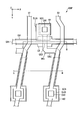
- FIG. 2 is a plan view showing the positional relationship of the second thin film transistors.
- FIG. 3 is a cross-sectional view showing the display device along the line AB shown in FIG.
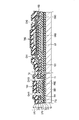
- FIG. 4 is a cross-sectional view showing the first thin film transistor in the non-display area and the second thin film transistor in the display area.
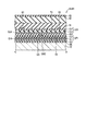
- FIG. 5 is a cross-sectional view showing the first substrate taken along the line CD shown in FIG.
- FIG. 6 is a cross-sectional view showing a step of forming a contact hole of the first thin film transistor and a contact hole of the second thin film transistor.
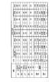
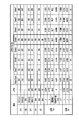
- FIG. 7 is a table showing the results of measuring the film thickness and optical characteristics of each display device.
- FIG. 8 is a table showing the results of measuring the film thickness and optical characteristics of each display device.
- the main configuration of this embodiment can be used for a display device.
- the display device can be used in various devices such as a smartphone, a tablet terminal, a mobile phone terminal, a notebook-type personal computer, an in-vehicle device, and a game device.
- the present embodiment is a liquid crystal display device, a self-luminous display device such as an organic electroluminescence display device, a micro LED display device, an electronic paper type display device having an electrophoretic element, a MEMS (Micro Electro Mechanical Systems).
- the present invention can be applied to various display devices such as a display device to which is applied or a display device to which electrochromism is applied. Further, the present invention can be applied to a wearable display device and a display device having an irregular shape.
- FIG. 1 is a diagram showing a configuration and an equivalent circuit of the display device DSP of this embodiment.
- the first direction X, the second direction Y, and the third direction Z are orthogonal to each other, but may intersect at an angle other than 90 degrees.
- the first direction X and the second direction Y correspond to the directions parallel to the main surface of the substrate forming the display device DSP
- the third direction Z corresponds to the thickness direction of the display device DSP.
- the direction toward the tip of the arrow indicating the third direction Z is referred to as upward (or simply upward), and the direction opposite from the tip of the arrow is referred to as downward (or simply downward).
- the display device DSP includes a display panel PNL and a wiring board WB mounted on the display panel PNL.
- the display panel PNL is a liquid crystal display panel, and includes a first substrate SUB1, a second substrate SUB2 facing the first substrate SUB1, a sealing material SE, a liquid crystal layer LC, a source line S, and a gate line G.
- the first thin film transistor TR1 and the second thin film transistor TR2, the pixel electrode PE, the common electrode CE and the like are provided.
- the display panel PNL includes a display area DA for displaying an image and a non-display area NDA surrounding the display area DA.
- the first substrate SUB1 has a mounting portion MA exposed outside the second substrate SUB2.
- the sealing material SE is located in the non-display area NDA and bonds the first substrate SUB1 and the second substrate SUB2 together.
- the region where the seal material SE is arranged is shown by a diagonal line rising to the right.
- the display area DA is located inside surrounded by the seal material SE.
- the display panel PNL includes a plurality of pixels PX arranged in a matrix in the first direction X and the second direction Y in the display area DA.
- the first thin film transistor TR1 functions as a switching element of a drive circuit for driving the pixel PX, and is located in the non-display area NDA.
- the first thin film transistor TR1 includes a semiconductor layer made of low temperature polysilicon (LTPS).
- the second thin film transistor TR2 functions as a switching element of the pixel PX and is located in the display area DA.
- the second thin film transistor TR2 includes an oxide semiconductor layer. That is, the display device DSP of the present embodiment has a hybrid structure including both the first thin film transistor TR1 using the LTPS and the second thin film transistor TR2 using the oxide semiconductor layer. The effect of applying the hybrid structure to the display device DSP will be described below.
- the first thin film transistor TR1 using LTPS having a high carrier mobility is suitable for the drive circuit of the non-display area NDA.
- an oxide semiconductor has low carrier mobility and thus may be difficult to use in a driver circuit. Therefore, the first thin film transistor TR1 using LTPS is used as the TFT of the drive circuit.
- the second thin film transistor TR2 using an oxide semiconductor is suitable for the pixel PX in the display area DA.
- the voltage is held for one frame by the holding capacitor CS formed between the pixel electrode PE and the electrode having the same potential as the common electrode CE.
- the leak current of the TFT is large, the voltage of the pixel electrode PE changes, and flicker or the like occurs to make it impossible to form a good image. That is, it is desirable that the TFT of the pixel PX has a small leak current.
- a TFT including an oxide semiconductor can reduce leakage current.
- the second thin film transistor TR2 including an oxide semiconductor is used as the TFT of the pixel PX.
- the first thin film transistor TR1 using LTPS is used for the driving circuit
- the second thin film transistor TR2 using oxide semiconductor is used for the pixel PX. Since such a display device DSP can reduce leakage current by the oxide semiconductor, it is excellent in low frequency driving, and power required for driving the display device DSP can be reduced.
- the above-mentioned source line S, gate line G, pixel electrode PE, common electrode CE, and liquid crystal layer LC are located in the display area DA.
- the source line S extends along the second direction Y
- the gate line G extends along the first direction X.
- the second thin film transistor TR2 is electrically connected to the gate line G and the source line S.
- the pixel electrode PE is electrically connected to the second thin film transistor TR2.
- Each of the pixel electrodes PE faces the common electrode CE and drives the liquid crystal layer LC by an electric field generated between the pixel electrode PE and the common electrode CE.
- the flexible wiring board WB is mounted on the mounting portion MA. Further, the wiring board WB includes a drive IC chip 2 that drives the display panel PNL. The drive IC chip 2 may be mounted on the mounting portion MA.
- the display panel PNL of the present embodiment is a transmissive type having a transmissive display function of displaying an image by selectively transmitting light from the back surface side of the first substrate SUB1, light from the front surface side of the second substrate SUB2. It may be either a reflective type having a reflective display function of displaying an image by selectively reflecting light or a semi-transmissive type having a transmissive display function and a reflective display function.
- the display panel PNL displays a display mode utilizing a lateral electric field along the main surface of the substrate and a vertical electric field along a normal line of the main surface of the substrate. It corresponds to the display mode to be used, the display mode to use the tilt electric field inclined in the oblique direction with respect to the main surface of the substrate, and the display mode to use the lateral electric field, the vertical electric field, and the tilt electric field in appropriate combination. It may have any configuration.
- the main surface of the substrate here is a surface parallel to the XY plane defined by the first direction X and the second direction Y.
- FIG. 2 is a plan view showing the positional relationship of the second thin film transistor TR2.
- the source lines S1 and S2 extend substantially in the second direction Y and are arranged in parallel in the first direction X.
- the gate lines G11 and G21 overlap each other and extend in the first direction X.
- the second thin film transistor TR2 is electrically connected to the gate line G21 and the source line S2.
- the second thin film transistor TR2 includes an oxide semiconductor layer OSC, source/drain electrodes EL21 and EL22, and protective electrodes 101 and 102.
- the oxide semiconductor layer OSC is arranged so that a part thereof overlaps the source line S2, and the other part extends between the source lines S1 and S2.
- the oxide semiconductor layer OSC intersects the gate lines G11 and G21 between the source lines S1 and S2. That is, the oxide semiconductor layer OSC overlaps with part of each of the gate lines G11 and G21.
- the gate line G11 has a light shielding film LS that is wide in the second direction Y.
- the oxide semiconductor layer OSC overlaps with the light shielding film LS.
- a region overlapping with the oxide semiconductor layer OSC functions as a second gate electrode GE2 described later.
- Protective electrode 101 overlaps one end SCA of oxide semiconductor layer OSC.
- the protective electrode 102 overlaps the source line S2 and the other end SCB of the oxide semiconductor layer OSC.
- the source/drain electrode EL21 is formed in an island shape and is arranged between the source line S1 and the source line S2.
- the source/drain electrode EL21 overlaps the protective electrode 101 and the one end portion SCA of the oxide semiconductor layer OSC.
- the source/drain electrode EL21 is electrically connected to the one end SCA through the through hole CH1.
- the source/drain electrode EL22 is formed integrally with the source line S2.
- the source/drain electrode EL22 overlaps the protective electrode 102 and the other end SCB of the oxide semiconductor layer OSC.
- the source/drain electrode EL22 is electrically connected to the other end SCB through the through hole CH2.
- FIG. 3 is a cross-sectional view showing the display device DSP taken along the line AB shown in FIG.
- the illustrated example corresponds to an example in which a display mode using a lateral electric field is applied to the display panel PNL.
- the display device DSP includes a first optical element OD1, a second optical element OD2, and an illumination device IL in addition to the display panel PNL.
- the first substrate SUB1 includes the insulating substrate 10, the undercoat layer UC, the first gate insulating film GI1, the first inorganic film IL1, the second inorganic film IL2, the second gate insulating film GI2, the third inorganic film IL3, and the fourth inorganic film.
- the film IL4 the first organic film 11, the second organic film 12, the capacitive insulating film 13, the oxide semiconductor layer OSC, the protective electrode 102, the source lines S1 and S2, the metal wirings ML1 and ML2, the common electrode CE, the pixel electrode PE,
- the alignment film AL1 is provided.
- the insulating substrate 10 is a light transmissive substrate such as a glass substrate or a flexible resin substrate.
- the undercoat layer UC is located on the insulating substrate 10.
- the first gate insulating film GI1 is located on the undercoat layer UC.
- the first inorganic film IL1 is located on the first gate insulating film GI1.
- the second inorganic film IL2 is located on the first inorganic film IL1.
- the oxide semiconductor layer OSC is located on the second inorganic film IL2.
- the protective electrode 102 covers the oxide semiconductor layer OSC.
- the second gate insulating film GI2 covers the protective electrode 102.
- the third inorganic film IL3 is located on the second gate insulating film GI2.
- the fourth inorganic film IL4 is located on the third inorganic film IL3.
- the source lines S1 and S2 are located on the fourth inorganic film IL4 and covered with the first organic film 11.
- the metal wirings ML1 and ML2 are located on the first organic film 11 and covered with the second organic film 12.
- the metal wirings ML1 and ML2 are located directly above the source lines S1 and S2, respectively.
- the common electrode CE is located on the second organic film 12 and covered with the capacitive insulating film 13.
- the pixel electrode PE is located on the capacitive insulating film 13 and covered with the alignment film AL1.
- the common electrode CE and the pixel electrode PE are transparent electrodes formed of a transparent conductive material such as indium tin oxide (ITO) and indium zinc oxide (IZO).
- the undercoat layer UC, the first gate insulating film GI1, the first inorganic film IL1, the second inorganic film IL2, the second gate insulating film GI2, the third inorganic film IL3, the fourth inorganic film IL4, and the capacitance insulating film 13 are made of silicon.
- the first organic film 11 and the second organic film 12 are organic insulating films formed of an organic insulating material such as acrylic resin, for example.
- the second substrate SUB2 includes an insulating substrate 20, a light shielding layer BM, a color filter CF, an overcoat layer OC, an alignment film AL2 and the like.
- the insulating substrate 20 is a light-transmissive substrate such as a glass substrate or a resin substrate.
- the light blocking layer BM and the color filter CF are located on the side of the insulating substrate 20 that faces the first substrate SUB1.
- the area where the light shielding layer BM is not located corresponds to the opening OP of the pixel.
- the color filter CF is arranged at a position facing the pixel electrode PE, and a part thereof overlaps the light shielding layer BM.
- the color filter CF has a red color filter CFR, a green color filter CFG, and a blue color filter CFB.
- the overcoat layer OC covers the color filter CF.
- the overcoat layer OC is formed of a transparent resin.
- the alignment film AL2 covers the overcoat layer OC.
- the alignment films AL1 and AL2 are formed of, for example, a material exhibiting horizontal alignment.
- the above-described first substrate SUB1 and second substrate SUB2 are arranged so that the alignment films AL1 and AL2 face each other.
- the first substrate SUB1 and the second substrate SUB2 are adhered by a sealing material with a predetermined cell gap formed.
- the liquid crystal layer LC is held between the alignment films AL1 and AL2.
- the liquid crystal layer LC includes liquid crystal molecules LM.
- the liquid crystal layer LC is made of a positive type (dielectric anisotropy is positive) liquid crystal material or a negative type (dielectric anisotropy is negative) liquid crystal material.
- the first optical element OD1 including the polarizing plate PL1 is adhered to the insulating substrate 10.
- the second optical element OD2 including the polarizing plate PL2 is adhered to the insulating substrate 20.
- the first optical element OD1 and the second optical element OD2 may be provided with a retardation plate, a scattering layer, an antireflection layer, etc., if necessary.
- the liquid crystal molecules LM are initially in a predetermined direction between the alignment films AL1 and AL2 in an off state where an electric field is not formed between the pixel electrode PE and the common electrode CE. It is oriented. In such an off state, the light emitted from the illumination device IL toward the display panel PNL is absorbed by the first optical element OD1 and the second optical element OD2, resulting in a dark display.
- the liquid crystal molecules LM are aligned in a direction different from the initial alignment direction by the electric field, and the alignment direction is controlled by the electric field. .. In such an ON state, a part of the light from the illumination device IL is transmitted through the first optical element OD1 and the second optical element OD2, resulting in bright display.
- FIG. 4 is a cross-sectional view showing the first thin film transistor TR1 in the non-display area NDA and the second thin film transistor TR2 in the display area DA. Both the first thin film transistor TR1 and the second thin film transistor TR2 are top gates.
- first inorganic film IL1 and the second inorganic film IL2 are combined to form a first inorganic laminated film LF1.
- third inorganic film IL3 and the fourth inorganic film IL4 are combined to form a second inorganic laminated film LF2.
- the first thin film transistor TR1 includes a polysilicon semiconductor layer PSC, a first gate electrode GE1 located on the polysilicon semiconductor layer PSC, and electrodes EL11 and EL12.
- the polysilicon semiconductor layer PSC is located on the undercoat layer UC and is covered with the first gate insulating film GI1.
- the undercoat layer UC is formed of, for example, two layers of SiO and SiN.
- the undercoat layer UC prevents impurities contained in the glass of the insulating substrate 10 from contaminating the polysilicon semiconductor layer PSC.
- the first gate insulating film GI1 is also located between the polysilicon semiconductor layer PSC and the first gate electrode GE1.
- the first gate insulating film GI1 is formed using, for example, tetraethoxysilane (TEOS).
- the first gate electrode GE1 is covered with the first inorganic film IL1.
- the first gate electrode GE1 is formed integrally with the gate line G11 shown in FIG.
- the electrodes EL11 and EL12 are located on the fourth inorganic film IL4 and are electrically connected to the polysilicon semiconductor layer PSC through the contact holes CH11 and CH12.
- the contact holes CH11 and CH12 overlap the polysilicon semiconductor layer PSC and penetrate the first gate insulating film GI1, the first inorganic laminated film LF1, the second gate insulating film GI2, and the second inorganic laminated film LF2 to the polysilicon semiconductor layer PSC. doing.
- the second thin film transistor TR2 includes an oxide semiconductor layer OSC, a second gate electrode GE2 located on the oxide semiconductor layer OSC, and source/drain electrodes EL21 and EL22.
- the light shielding film LS is located on the first gate insulating film GI1 and is covered with the first inorganic film IL1.
- the light shielding film LS is located below the oxide semiconductor layer OSC. Therefore, exposure of the oxide semiconductor layer OSC to light from the lighting device can be suppressed, and a photocurrent can be suppressed from flowing to the oxide semiconductor layer OSC.
- the light shielding film LS is located in the same layer as the first gate electrode GE1 and is made of the same material.
- TAOS Transparent Amorphous Oxide Semiconductor
- IGZO Indium Gallium Zinc Oxide
- ITZO Indium Tin Zinc Oxide
- ZnON Zinc Oxide Nitride
- IGO Indium Gallium Oxide
- the first inorganic film IL1 is in contact with the light shielding film LS and the first gate insulating film GI1.
- the second inorganic film IL2 is stacked on the first inorganic film IL1 and is in contact with the oxide semiconductor layer OSC.
- the first inorganic film IL1 is made of, for example, SiN.
- the second inorganic film IL2 is made of, for example, SiO.
- the first inorganic film IL1 may be formed of SiON instead of SiN.
- the film thickness of the first inorganic film IL1 and the second inorganic film IL2 either one may be thicker than the other depending on the purpose.
- the third inorganic film IL3 is in contact with the second gate electrode GE2 and the second gate insulating film GI2.
- the fourth inorganic film IL4 is stacked on the third inorganic film IL3.
- the third inorganic film IL3 is made of, for example, SiN.
- the fourth inorganic film IL4 is made of, for example, SiO.
- the lower inorganic film be SiN and the upper inorganic film be SiO.
- the third inorganic film IL3 may be formed of SiON instead of SiN.
- the film thickness of the third inorganic film IL3 and the fourth inorganic film IL4 either one may be thicker than the other depending on the purpose.
- the second gate insulating film GI2 is also located between the oxide semiconductor layer OSC and the second gate electrode GE2. That is, the second gate insulating film GI2 covers the entire oxide semiconductor layer OSC and is also formed in regions other than the contact holes CH1, CH2, CH11, and CH12. The second gate insulating film GI2 is also located in the opening OP, as shown in FIG. The second gate insulating film GI2 is in contact with the second inorganic film IL2, but since it is formed of SiO similarly to the second inorganic film IL2, the second gate insulating film GI2 has the same refractive index and is unlikely to affect thin film interference.
- the source/drain electrodes EL21, EL22 are located on the fourth inorganic film IL4 and are in contact with the protective electrodes 101, 102 through the contact holes CH1, CH2, respectively.
- the contact holes CH1 and CH2 overlap the oxide semiconductor layer OSC and penetrate the second gate insulating film GI2 and the second inorganic laminated film LF2 to the protective electrodes 101 and 102.
- the first organic film 11 covers the electrodes EL11, EL12 and the source/drain electrodes EL21, EL22.
- the pixel electrode PE is connected to the source/drain electrode EL21 through a contact hole CH3 penetrating the first organic film 11, the second organic film 12, and the capacitive insulating film 13.
- the second gate insulating film GI2 is uniformly formed not only under the second gate electrode GE2 but also in a region other than the contact hole. Therefore, in implantation of the oxide semiconductor layer OSC, the resistance of the oxide semiconductor layer OSC can be stably reduced.
- the inorganic film in contact with the oxide semiconductor layer OSC is SiN, hydrogen in the oxide semiconductor layer OSC may be released. Since the second gate insulating film GI2 is in contact with the oxide semiconductor layer OSC and formed of SiO, release of hydrogen from the oxide semiconductor layer OSC can be suppressed. Therefore, deterioration of the characteristics of the oxide semiconductor layer OSC can be suppressed.
- the total thickness of the first gate insulating film GI1 and the second gate insulating film GI2 is smaller than the total thickness of the first inorganic laminated film LF1 and the second inorganic laminated film LF2.
- the thickness of the first inorganic laminated film LF1 is larger than that of the first gate electrode GE1 and the thickness of the second inorganic laminated film LF2 is larger than that of the second gate electrode GE2, the insulation properties of the gate line and the gate electrode are secured. it can.
- FIG. 5 is a cross-sectional view showing the first substrate SUB1 taken along the line CD shown in FIG.
- the oxide semiconductor layer OSC and the gate line G11 intersect with each other, a capacitance is generated between them.
- the gate line G21 intersects the source lines S1 and S2, capacitance is generated between the gate line G21 and the source line S1 and between the gate line G21 and the source line S2. If these capacities are large, there is a risk that the power for driving the pixels will increase.
- the thickness T1 of the first inorganic laminated film LF1 is set to 300 nm or more in order to reduce the capacitance between the oxide semiconductor layer OSC and the gate line G11. Further, in order to reduce the capacitance between the gate line G21 and the source line S1 and between the gate line G21 and the source line S2, the film thickness T2 of the second inorganic laminated film LF2 is set to 400 nm or more. By reducing the capacity, the original power reduction effect of the hybrid structure can be obtained.
- FIG. 6 is a cross-sectional view showing a step of forming the contact holes CH11, CH12 of the first thin film transistor TR1 and the contact holes CH1, CH2 of the second thin film transistor TR2.
- Contact holes CH1, CH2, CH11, CH12 are formed in the same process by dry etching. Dry etching is performed using a CF-based (CF4) or CHF-based (CHF3) gas. At the time of dry etching, the oxide semiconductor layer OSC is protected by the protective electrodes 101 and 102 and is not removed.
- the contact holes CH11 and CH12 penetrate the first gate insulating film GI1, the first inorganic laminated film LF1, the second gate insulating film GI2, and the second inorganic laminated film LF2, and the contact holes CH1 and CH2 are the second It penetrates through the gate insulating film GI2 and the second inorganic laminated film LF2. Therefore, the contact holes CH11 and CH12 are cut deeper than the contact holes CH1 and CH2 by the film thickness of the first gate insulating film GI1 and the first inorganic laminated film LF1.
- the contact holes CH1, CH2 may be overcut while the contact holes CH11, CH12 are cut.
- the contact holes CH1 and CH2 are excessively cut, the source/drain electrodes are not able to follow the shapes of the contact holes CH1 and CH2 and are broken, or the source/drain electrodes are formed according to the sizes of the contact holes CH1 and CH2. Since it is necessary, the aperture ratio of the pixel may decrease. In addition, the strength of the lighting device must be increased as the aperture ratio decreases, which may increase power consumption.
- the film thickness T1 of the first inorganic laminated film LF1 is set to the second inorganic laminated film. It is formed thinner than the film thickness T2 of LF2. More specifically, the film thickness of the first inorganic laminated film LF1 is 500 nm or less. Furthermore, in order to secure the processability of the contact holes CH11 and CH12, the total thickness of the first gate insulating film GI1, the first inorganic laminated film LF1, the second gate insulating film GI2, and the second inorganic laminated film LF2 is It is 1100 nm or less.
- the etching rate of the first inorganic laminated film LF1 is higher.
- SiN has a faster etching rate than SiO. Therefore, it is desirable that the first inorganic laminated film LF1 satisfy the relationship that the film thickness of SiN is larger than the film thickness of SiO.
- the film thickness T11 of the first inorganic film IL1 is formed larger than the film thickness T12 of the second inorganic film IL2. .. Therefore, excessive etching of the contact holes CH1 and CH2 can be suppressed. Therefore, it is possible to suppress disconnection of the source/drain electrodes, decrease in pixel aperture ratio, and increase in power consumption.
- FIG. 7 is a table showing the results of measuring the film thickness and optical characteristics of each display device.
- the second gate insulating film GI2 and the second inorganic laminated film LF2 are not formed.
- the film thickness condition of the second embodiment satisfies the film thickness of the first inorganic laminated film LF1 of 300 nm or more and the film thickness of the second inorganic laminated film LF2 of 400 nm or more.
- the film thickness of the first inorganic laminated film LF1 which is the film thickness condition of the third embodiment is 500 nm or less, the first gate insulating film GI1, the first inorganic laminated film LF1, the second gate insulating film GI2, The total thickness of the second inorganic laminated film LF2 satisfies 1100 nm or less.
- the transmittance Y is lower than in LTPS, and the values of chromaticity x and y are also changed.
- the film thickness conditions of the second embodiment and the third embodiment may not be satisfied.
- x is preferably 0.006 or less and y is preferably 0.01 or less.
- Case1, Case3, Case5, Case6, Case7 satisfy this.
- Case 1 has a better 4 ⁇ than Case 6, but has a drawback that it is difficult to use because x of the optical type is 0.003 smaller than LTPS.
- Case 5 and Case 7 are inferior to Case 6 in both Type and 4 ⁇ . Therefore, Case3 and Case6 are optimal from the viewpoint of optical type and optical 4 ⁇ .
- the transmittance can be improved over LTPS while maintaining the chromaticity close to LTPS.
- the number of laminated insulating films having different refractive indexes is larger than that in the case of only LTPS. Therefore, the thin film interference may reduce the transmittance, which may increase the power consumption of the lighting device.
- optical interference is optimized and optical characteristics are improved by changing the total thickness of the first inorganic laminated film LF1, the total thickness of the second inorganic laminated film LF2, and the film thickness ratio of SiN and SiO. be able to.
- the first inorganic film IL1 has a thickness of 275 nm
- the second inorganic film IL2 has a thickness of 225 nm
- the thickness of the first inorganic film IL1 is thicker than that of the second inorganic film IL2.
- the total thickness of the first inorganic laminated film LF1 is 500 nm
- the film thickness ratio of SiO and SiN is 9:11. That is, SiN has a film thickness of about 1.2 times that of SiO.
- the third inorganic film IL3 has a thickness of 150 nm
- the fourth inorganic film IL4 has a thickness of 250 nm
- the film thickness of the third inorganic film IL3 is thinner than the film thickness of the fourth inorganic film IL4.
- the total thickness of the second inorganic laminated film LF2 is 400 nm
- the film thickness ratio of SiO and SiN is 5:3. That is, SiN is 0.6 times as large as SiO.
- the first inorganic film IL1 has a thickness of 150 nm
- the second inorganic film IL2 has a thickness of 250 nm
- the thickness of the first inorganic film IL1 is smaller than that of the second inorganic film IL2.
- the total thickness of the first inorganic laminated film LF1 is 400 nm
- the film thickness ratio of SiO and SiN is 5:3. That is, SiN has a film thickness 0.6 times that of SiO.
- the film thickness of the second inorganic laminated film LF2 and the film thickness ratio of SiO and SiN are the same as in Case 3.
- the optical interference may be further optimized by changing SiN to SiON.
- FIG. 8 is a table showing the results of measuring the film thickness and optical characteristics of each display device.
- Base Case Case 2, Case 3, Case 4, and Case 6 are preferable.
- the chromaticity deviation amount ⁇ xy is large.
- Case2, Case3, Case4, and Case6, Case4 is optimal from the viewpoint of optical type and optical 4 ⁇ .
- the first inorganic film IL1 is 420 nm
- the second inorganic film IL2 is 100 nm
- the film thickness of the first inorganic film IL1 is thicker than the film thickness of the second inorganic film IL2.
- the total thickness of the first inorganic laminated film LF1 is 520 nm, and the film thickness ratio of SiO and SiN is 5:21. That is, SiN has a film thickness 4.2 times that of SiO.
- the third inorganic film IL3 has a thickness of 280 nm
- the fourth inorganic film IL4 has a thickness of 120 nm
- the film thickness of the third inorganic film IL3 is thicker than the film thickness of the fourth inorganic film IL4.
- the total thickness of the second inorganic laminated film LF2 is 400 nm
- the film thickness ratio of SiO and SiN is 3:7. That is, SiN is about 2.3 times as much as SiO.
- the display device capable of reducing the power consumption.
Landscapes
- Physics & Mathematics (AREA)
- Nonlinear Science (AREA)
- General Physics & Mathematics (AREA)
- Optics & Photonics (AREA)
- Mathematical Physics (AREA)
- Chemical & Material Sciences (AREA)
- Crystallography & Structural Chemistry (AREA)
- Engineering & Computer Science (AREA)
- Liquid Crystal (AREA)
- Microelectronics & Electronic Packaging (AREA)
- Theoretical Computer Science (AREA)
- Devices For Indicating Variable Information By Combining Individual Elements (AREA)
- Metal-Oxide And Bipolar Metal-Oxide Semiconductor Integrated Circuits (AREA)
- Thin Film Transistor (AREA)
Abstract
本実施形態に係る表示装置は、画像を表示する表示領域と、前記表示領域を囲む非表示領域と、を有し、ポリシリコン半導体層と、前記ポリシリコン半導体層の上に位置する第1ゲート電極と、を有し、前記非表示領域に位置する第1薄膜トランジスタと、酸化物半導体層と、前記酸化物半導体層の上に位置する第2ゲート電極と、を有し、前記表示領域に位置する第2薄膜トランジスタと、前記ポリシリコン半導体層と前記第1ゲート電極との間に位置する第1ゲート絶縁膜と、前記酸化物半導体層と前記第2ゲート電極との間に位置する第2ゲート絶縁膜と、を備え、前記第2ゲート絶縁膜は、前記酸化物半導体層全体を覆っている。
Description
本発明の実施形態は、表示装置に関する。
表示装置は、画像を表示する表示領域において画素を備え、表示領域の周辺の非表示領域において駆動回路を備えている。画素のスイッチング素子として用いられる薄膜トランジスタ(TFT)は、リーク電流が小さいことが必要である。酸化物半導体によるTFTは、リーク電流を小さくすることができる。一方、駆動回路に用いられるTFTは、移動度が大きいことが望ましい。LTPS(Low Temperature Poly-Si)で形成したTFTは移動度が大きいため、駆動回路に用いることができる。このように、表示領域における画素のTFTに酸化物半導体を用い、周辺駆動回路のTFTにLTPSを用いる構成が知られている。
本実施形態の目的は、消費電力を小さくすることが可能な表示装置を提供することにある。
本実施形態によれば、画像を表示する表示領域と、前記表示領域を囲む非表示領域と、を有し、ポリシリコン半導体層と、前記ポリシリコン半導体層の上に位置する第1ゲート電極と、を有し、前記非表示領域に位置する第1薄膜トランジスタと、酸化物半導体層と、前記酸化物半導体層の上に位置する第2ゲート電極と、を有し、前記表示領域に位置する第2薄膜トランジスタと、前記ポリシリコン半導体層と前記第1ゲート電極との間に位置する第1ゲート絶縁膜と、前記酸化物半導体層と前記第2ゲート電極との間に位置する第2ゲート絶縁膜と、を備え、前記第2ゲート絶縁膜は、前記酸化物半導体層全体を覆っている、表示装置が提供される。
以下、本実施形態について、図面を参照しながら説明する。なお、開示はあくまで一例に過ぎず、当業者において、発明の主旨を保っての適宜変更について容易に想到し得るものについては、当然に本発明の範囲に含有されるものである。また、図面は、説明をより明確にするため、実際の態様に比べて、各部の幅、厚さ、形状等について模式的に表される場合があるが、あくまで一例であって、本発明の解釈を限定するものではない。また、本明細書と各図において、既出の図に関して前述したものと同一又は類似した機能を発揮する構成要素には同一の参照符号を付し、重複する詳細な説明を適宜省略することがある。
本実施形態の主要な構成は、表示装置に用いることができる。この表示装置は、例えば、スマートフォン、タブレット端末、携帯電話端末、ノートブックタイプのパーソナルコンピュータ、車載機器、ゲーム機器等の種々の装置に用いることができる。また、本実施形態は、液晶表示装置、有機エレクトロルミネッセンス表示装置等の自発光型の表示装置、マイクロLED表示装置、電気泳動素子等を有する電子ペーパ型の表示装置、MEMS(Micro Electro Mechanical Systems)を応用した表示装置、或いはエレクトロクロミズムを応用した表示装置など、種々の表示装置に適用可能である。また、ウェアラブルの表示装置や異形状の表示装置にも適用可能である。
[第1実施形態]
図1は、本実施形態の表示装置DSPの構成及び等価回路を示す図である。
一例では、第1方向X、第2方向Y、及び、第3方向Zは、互いに直交しているが、90度以外の角度で交差していてもよい。第1方向X及び第2方向Yは、表示装置DSPを構成する基板の主面と平行な方向に相当し、第3方向Zは、表示装置DSPの厚さ方向に相当する。本明細書において、第3方向Zを示す矢印の先端に向かう方向を上方(あるいは、単に上)と称し、矢印の先端から逆に向かう方向を下方(あるいは、単に下)と称する。
図1は、本実施形態の表示装置DSPの構成及び等価回路を示す図である。
一例では、第1方向X、第2方向Y、及び、第3方向Zは、互いに直交しているが、90度以外の角度で交差していてもよい。第1方向X及び第2方向Yは、表示装置DSPを構成する基板の主面と平行な方向に相当し、第3方向Zは、表示装置DSPの厚さ方向に相当する。本明細書において、第3方向Zを示す矢印の先端に向かう方向を上方(あるいは、単に上)と称し、矢印の先端から逆に向かう方向を下方(あるいは、単に下)と称する。
表示装置DSPは、表示パネルPNLと、表示パネルPNLに実装された配線基板WBと、を備えている。表示パネルPNLは、液晶表示パネルであり、第1基板SUB1と、第1基板SUB1と対向する第2基板SUB2と、シール材SEと、液晶層LCと、ソース線Sと、ゲート線Gと、第1薄膜トランジスタTR1及び第2薄膜トランジスタTR2と、画素電極PEと、共通電極CEなどを備えている。また、表示パネルPNLは、画像を表示する表示領域DAと、表示領域DAを囲む非表示領域NDAと、を備えている。
第1基板SUB1は、第2基板SUB2よりも外側に露出した実装部MAを有している。シール材SEは、非表示領域NDAに位置し、第1基板SUB1と第2基板SUB2とを接着している。図1において、シール材SEが配置された領域は右上がり斜線で示されている。表示領域DAは、シール材SEによって囲まれた内側に位置している。表示パネルPNLは、表示領域DAにおいて第1方向X及び第2方向Yにマトリクス状に配置された複数の画素PXを備えている。
第1薄膜トランジスタTR1は、画素PXを駆動するための駆動回路のスイッチング素子として機能し、非表示領域NDAに位置している。第1薄膜トランジスタTR1は、低温ポリシリコン(LTPS)を用いた半導体層を備えている。一方、第2薄膜トランジスタTR2は、画素PXのスイッチング素子として機能し、表示領域DAに位置している。第2薄膜トランジスタTR2は、酸化物半導体層を備えている。すなわち、本実施形態の表示装置DSPは、LTPSを用いた第1薄膜トランジスタTR1と、酸化物半導体層を用いた第2薄膜トランジスタTR2の両者によるハイブリッド構造を有している。以下にハイブリット構造が表示装置DSPに適用される効果を述べる。
非表示領域NDAの駆動回路には、キャリアの移動度が大きいLTPSを用いた第1薄膜トランジスタTR1が適している。一方、酸化物半導体はキャリアの移動度が小さいため、駆動回路に用いるのは難しい場合がある。よって、LTPSを用いた第1薄膜トランジスタTR1が駆動回路のTFTとして用いられる。
表示領域DAの画素PXには、酸化物半導体を用いた第2薄膜トランジスタTR2が適している。画素電極PEに映像信号が書き込まれると、画素電極PE及び共通電極CEと同電位の電極間に形成される保持容量CSによって、1フレームの間、電圧が保持される。この時、TFTのリーク電流が大きいと、画素電極PEの電圧が変化し、フリッカ等が発生して良好な画像を形成できなくなる。すなわち、画素PXのTFTは、リーク電流が小さいことが望ましい。酸化物半導体によるTFTは、リーク電流を小さくすることができる。一方、LTPSはリーク電流が大きいため、画素PXのTFTとして使用する場合には、2個のLTPSを直列にして使用しなければならない場合がある。よって、酸化物半導体を用いた第2薄膜トランジスタTR2が画素PXのTFTとして用いられる。以上より、LTPSを用いた第1薄膜トランジスタTR1が駆動回路に使用され、酸化物半導体を用いた第2薄膜トランジスタTR2が画素PXに使用されている。このような表示装置DSPは、酸化物半導体によってリーク電流を小さくすることができるため、低周波駆動に優れており、表示装置DSPの駆動に必要な電力を削減することができる。
上記したソース線S、ゲート線G、画素電極PE、共通電極CE、液晶層LCは、表示領域DAに位置している。ソース線Sは第2方向Yに沿って延出し、ゲート線Gは第1方向Xに沿って延出している。第2薄膜トランジスタTR2は、ゲート線G及びソース線Sと電気的に接続されている。画素電極PEは、第2薄膜トランジスタTR2と電気的に接続されている。画素電極PEの各々は、共通電極CEと対向し、画素電極PEと共通電極CEとの間に生じる電界によって液晶層LCを駆動している。
フレキシブルな配線基板WBは、実装部MAに実装されている。また、配線基板WBは、表示パネルPNLを駆動する駆動ICチップ2を備えている。なお、駆動ICチップ2は、実装部MAに実装されても良い。
本実施形態の表示パネルPNLは、第1基板SUB1の背面側からの光を選択的に透過させることで画像を表示する透過表示機能を備えた透過型、第2基板SUB2の前面側からの光を選択的に反射させることで画像を表示する反射表示機能を備えた反射型、あるいは、透過表示機能及び反射表示機能を備えた半透過型のいずれであってもよい。
また、表示パネルPNLの詳細な構成について、ここでは説明を省略するが、表示パネルPNLは、基板主面に沿った横電界を利用する表示モード、基板主面の法線に沿った縦電界を利用する表示モード、基板主面に対して斜め方向に傾斜した傾斜電界を利用する表示モード、さらには、上記の横電界、縦電界、及び、傾斜電界を適宜組み合わせて利用する表示モードに対応したいずれの構成を備えていてもよい。ここでの基板主面とは、第1方向X及び第2方向Yで規定されるX-Y平面と平行な面である。
図2は、第2薄膜トランジスタTR2の位置関係を示す平面図である。
ソース線S1及びS2は、概ね第2方向Yに延出し、第1方向Xに並列している。ゲート線G11及びG21は、互いに重なり、第1方向Xに延出している。第2薄膜トランジスタTR2は、ゲート線G21及びソース線S2と電気的に接続されている。第2薄膜トランジスタTR2は、酸化物半導体層OSCと、ソース・ドレイン電極EL21、EL22と、保護電極101、102などを備えている。
ソース線S1及びS2は、概ね第2方向Yに延出し、第1方向Xに並列している。ゲート線G11及びG21は、互いに重なり、第1方向Xに延出している。第2薄膜トランジスタTR2は、ゲート線G21及びソース線S2と電気的に接続されている。第2薄膜トランジスタTR2は、酸化物半導体層OSCと、ソース・ドレイン電極EL21、EL22と、保護電極101、102などを備えている。
酸化物半導体層OSCは、その一部分がソース線S2と重なるように配置され、他の部分がソース線S1とS2との間に延出している。酸化物半導体層OSCは、ソース線S1とS2との間においてゲート線G11及びG21と交差している。すなわち、酸化物半導体層OSCは、ゲート線G11及びG21のそれぞれの一部と重なっている。ゲート線G11は、第2方向Yに幅広になった遮光膜LSを有している。酸化物半導体層OSCは、遮光膜LSと重なっている。また、ゲート線G21において、酸化物半導体層OSCと重畳する領域が後述する第2ゲート電極GE2として機能する。
保護電極101は、酸化物半導体層OSCの一端部SCAに重なっている。保護電極102は、ソース線S2に重なり、酸化物半導体層OSCの他端部SCBに重なっている。ソース・ドレイン電極EL21は、島状に形成され、ソース線S1とソース線S2との間に配置されている。ソース・ドレイン電極EL21は、保護電極101と、酸化物半導体層OSCの一端部SCAと重なっている。ソース・ドレイン電極EL21は、貫通孔CH1を通じて一端部SCAと電気的に接続されている。ソース・ドレイン電極EL22は、ソース線S2と一体的に形成されている。ソース・ドレイン電極EL22は、保護電極102と、酸化物半導体層OSCの他端部SCBと重なっている。ソース・ドレイン電極EL22は、貫通孔CH2を通じて他端部SCBと電気的に接続されている。
図3は、図2に示したA-B線における表示装置DSPを示す断面図である。
図示した例は、表示パネルPNLに横電界を利用する表示モードが適用された例に相当する。表示装置DSPは、表示パネルPNLに加えて、第1光学素子OD1、第2光学素子OD2、照明装置ILを備えている。
図示した例は、表示パネルPNLに横電界を利用する表示モードが適用された例に相当する。表示装置DSPは、表示パネルPNLに加えて、第1光学素子OD1、第2光学素子OD2、照明装置ILを備えている。
第1基板SUB1は、絶縁基板10、アンダーコート層UC、第1ゲート絶縁膜GI1、第1無機膜IL1、第2無機膜IL2、第2ゲート絶縁膜GI2、第3無機膜IL3、第4無機膜IL4、第1有機膜11、第2有機膜12、容量絶縁膜13、酸化物半導体層OSC、保護電極102、ソース線S1及びS2、金属配線ML1及びML2、共通電極CE、画素電極PE、配向膜AL1を備えている。
絶縁基板10は、ガラス基板や可撓性の樹脂基板などの光透過性を有する基板である。アンダーコート層UCは、絶縁基板10の上に位置している。第1ゲート絶縁膜GI1は、アンダーコート層UCの上に位置している。第1無機膜IL1は、第1ゲート絶縁膜GI1の上に位置している。第2無機膜IL2は、第1無機膜IL1の上に位置している。酸化物半導体層OSCは、第2無機膜IL2の上に位置している。保護電極102は、酸化物半導体層OSCを覆っている。第2ゲート絶縁膜GI2は、保護電極102の上を覆っている。第3無機膜IL3は、第2ゲート絶縁膜GI2の上に位置している。第4無機膜IL4は、第3無機膜IL3の上に位置している。ソース線S1及びS2は、第4無機膜IL4の上に位置し、第1有機膜11によって覆われている。金属配線ML1及びML2は、第1有機膜11の上に位置し、第2有機膜12によって覆われている。金属配線ML1及びML2は、それぞれソース線S1及びS2の直上に位置している。共通電極CEは、第2有機膜12の上に位置し、容量絶縁膜13によって覆われている。画素電極PEは、容量絶縁膜13の上に位置し、配向膜AL1によって覆われている。共通電極CE及び画素電極PEは、インジウム・ティン・オキサイド(ITO)やインジウム・ジンク・オキサイド(IZO)などの透明な導電材料によって形成された透明電極である。
アンダーコート層UC、第1ゲート絶縁膜GI1、第1無機膜IL1、第2無機膜IL2、第2ゲート絶縁膜GI2、第3無機膜IL3、第4無機膜IL4、容量絶縁膜13は、シリコン酸化物(SiO)、シリコン窒化物(SiN)、シリコン酸窒化物(SiON)などの無機絶縁材料によって形成された無機絶縁膜であり、単層構造であってもよいし、多層構造であってもよい。第1有機膜11、第2有機膜12は、例えば、アクリル樹脂などの有機絶縁材料によって形成された有機絶縁膜である。
第2基板SUB2は、絶縁基板20、遮光層BM、カラーフィルタCF、オーバーコート層OC、配向膜AL2などを備えている。絶縁基板20は、絶縁基板10と同様に、ガラス基板や樹脂基板などの光透過性を有する基板である。遮光層BM及びカラーフィルタCFは、絶縁基板20の第1基板SUB1と対向する側に位置している。表示領域DAにおいて、遮光層BMが位置しない領域が画素の開口部OPに相当する。カラーフィルタCFは、画素電極PEと対向する位置に配置され、その一部が遮光層BMに重なっている。カラーフィルタCFは、赤色のカラーフィルタCFR、緑色のカラーフィルタCFG、青色のカラーフィルタCFBを有している。オーバーコート層OCは、カラーフィルタCFを覆っている。オーバーコート層OCは、透明な樹脂によって形成されている。配向膜AL2は、オーバーコート層OCを覆っている。配向膜AL1及び配向膜AL2は、例えば、水平配向性を呈する材料によって形成されている。
上述した第1基板SUB1及び第2基板SUB2は、配向膜AL1及び配向膜AL2が対向するように配置されている。第1基板SUB1及び第2基板SUB2は、所定のセルギャップが形成された状態でシール材によって接着されている。液晶層LCは、配向膜AL1と配向膜AL2との間に保持されている。液晶層LCは、液晶分子LMを備えている。液晶層LCは、ポジ型(誘電率異方性が正)の液晶材料、あるいは、ネガ型(誘電率異方性が負)の液晶材料によって構成されている。
偏光板PL1を含む第1光学素子OD1は、絶縁基板10に接着されている。偏光板PL2を含む第2光学素子OD2は、絶縁基板20に接着されている。なお、第1光学素子OD1及び第2光学素子OD2は、必要に応じて位相差板、散乱層、反射防止層などを備えていてもよい。
このような表示パネルPNLにおいては、画素電極PEと共通電極CEとの間に電界が形成されていないオフ状態において、液晶分子LMは、配向膜AL1及び配向膜AL2の間で所定の方向に初期配向している。このようなオフ状態では、照明装置ILから表示パネルPNLに向けて照射された光は、第1光学素子OD1及び第2光学素子OD2によって吸収され、暗表示となる。一方、画素電極PEと共通電極CEとの間に電界が形成されたオン状態においては、液晶分子LMは、電界により初期配向方向とは異なる方向に配向し、その配向方向は電界によって制御される。このようなオン状態では、照明装置ILからの光の一部は、第1光学素子OD1及び第2光学素子OD2を透過し、明表示となる。
図4は、非表示領域NDAの第1薄膜トランジスタTR1と、表示領域DAの第2薄膜トランジスタTR2を示す断面図である。第1薄膜トランジスタTR1及び第2薄膜トランジスタTR2は何れもトップゲートである。
ここで、第1無機膜IL1と第2無機膜IL2を合わせて第1無機積層膜LF1とする。また、第3無機膜IL3と第4無機膜IL4を合わせて第2無機積層膜LF2とする。
まず、非表示領域NDAに着目して第1薄膜トランジスタTR1の構成について説明する。第1薄膜トランジスタTR1は、ポリシリコン半導体層PSCと、ポリシリコン半導体層PSCの上に位置する第1ゲート電極GE1と、電極EL11、EL12と、を有している。ポリシリコン半導体層PSCは、アンダーコート層UCの上に位置し、第1ゲート絶縁膜GI1によって覆われている。アンダーコート層UCは、例えば、SiOとSiNの2層から形成されている。アンダーコート層UCは、絶縁基板10のガラスに含まれる不純物がポリシリコン半導体層PSCを汚染することを防止する。第1ゲート絶縁膜GI1は、ポリシリコン半導体層PSCと第1ゲート電極GE1との間にも位置している。第1ゲート絶縁膜GI1は、例えば、テトラエトキシシラン(TEOS)を用いて形成されている。第1ゲート電極GE1は、第1無機膜IL1によって覆われている。第1ゲート電極GE1は、図2に示したゲート線G11と一体的に形成されている。電極EL11、EL12は、第4無機膜IL4の上に位置し、コンタクトホールCH11、CH12を介してポリシリコン半導体層PSCと電気的に接続されている。コンタクトホールCH11、CH12は、ポリシリコン半導体層PSCに重なり、第1ゲート絶縁膜GI1、第1無機積層膜LF1、第2ゲート絶縁膜GI2、第2無機積層膜LF2をポリシリコン半導体層PSCまで貫通している。
次に、表示領域DAに着目して第2薄膜トランジスタTR2の構成について説明する。第2薄膜トランジスタTR2は、酸化物半導体層OSCと、酸化物半導体層OSCの上に位置する第2ゲート電極GE2と、ソース・ドレイン電極EL21、EL22と、を有している。遮光膜LSは、第1ゲート絶縁膜GI1の上に位置し、第1無機膜IL1によって覆われている。遮光膜LSは、酸化物半導体層OSCの下に位置している。そのため、酸化物半導体層OSCが照明装置からの光に晒されるのを抑制し、酸化物半導体層OSCに光電流が流れるのを抑制することができる。また、遮光膜LSは、第1ゲート電極GE1と同層に位置し、同一材料によって形成されている。
酸化物半導体層OSCとしては、例えば、TAOS(Transparent Amorphous Oxide Semiconductor)が用いられる。TAOSとしては、IGZO(Indium Gallium Zinc Oxide)、ITZO(Indium Tin Zinc Oxide)、ZnON(Zinc Oxide Nitride)、IGO(Indium Gallium Oxide)等やこれらの組み合わせが用いられる。
第1無機膜IL1は、遮光膜LS及び第1ゲート絶縁膜GI1に接している。第2無機膜IL2は、第1無機膜IL1に積層され、酸化物半導体層OSCに接している。第1無機膜IL1は、例えば、SiNによって形成されている。第2無機膜IL2は、例えば、SiOによって形成されている。第1無機積層膜LF1は、酸化物半導体層OSCのチャネル部の水素吸着によるTFT閾値マイナスシフトを回避するため、下の無機膜をSiN、上の無機膜をSiOとすることが望ましい。また、薄膜干渉の観点から、第1無機膜IL1は、SiNの代わりに、SiONによって形成されていても良い。第1無機膜IL1及び第2無機膜IL2の膜厚は、目的に応じて、どちらか一方がもう一方より厚くても良い。
第3無機膜IL3は、第2ゲート電極GE2及び第2ゲート絶縁膜GI2に接している。第4無機膜IL4は、第3無機膜IL3に積層されている。第3無機膜IL3は、例えば、SiNによって形成されている。第4無機膜IL4は、例えば、SiOによって形成されている。第2無機積層膜LF2は、酸化物半導体層OSCのチャネル部以外の低抵抗化のため、下の無機膜をSiN、上の無機膜をSiOとすることが望ましい。また、薄膜干渉の観点から、第3無機膜IL3は、SiNの代わりに、SiONによって形成されていても良い。第3無機膜IL3及び第4無機膜IL4の膜厚は、目的に応じて、どちらか一方がもう一方より厚くても良い。
第2ゲート絶縁膜GI2は、酸化物半導体層OSCと第2ゲート電極GE2との間にも位置している。すなわち、第2ゲート絶縁膜GI2は、酸化物半導体層OSC全体を覆っており、コンタクトホールCH1、CH2、CH11、CH12以外の領域にも形成されている。第2ゲート絶縁膜GI2は、図3に示すように、開口部OPにも位置している。第2ゲート絶縁膜GI2は、第2無機膜IL2に接しているが、第2無機膜IL2と同様にSiOによって形成されるため、互いに屈折率が等しく薄膜干渉に影響しにくい。
ソース・ドレイン電極EL21、EL22は、第4無機膜IL4の上に位置し、コンタクトホールCH1、CH2を通じてそれぞれ保護電極101、102に接している。コンタクトホールCH1、CH2は、酸化物半導体層OSCに重なり、第2ゲート絶縁膜GI2、第2無機積層膜LF2を保護電極101、102まで貫通している。
第1有機膜11は、電極EL11、EL12、ソース・ドレイン電極EL21、EL22を覆っている。画素電極PEは、第1有機膜11、第2有機膜12、容量絶縁膜13を貫通するコンタクトホールCH3を通じてソース・ドレイン電極EL21に接続されている。
本実施形態によれば、第2ゲート絶縁膜GI2は、第2ゲート電極GE2の下だけではなく、コンタクトホール以外の領域に一様に形成されている。そのため、酸化物半導体層OSCのインプランテーションにおいて、酸化物半導体層OSCを安定的に低抵抗化することができる。また、酸化物半導体層OSCに接する無機膜がSiNである場合、酸化物半導体層OSCの水素を放出する恐れがある。第2ゲート絶縁膜GI2は、酸化物半導体層OSCに接し、SiOで形成されているため、酸化物半導体層OSCの水素の放出を抑制することができる。よって、酸化物半導体層OSCの特性の劣化を抑制することができる。第2無機膜IL2についても、酸化物半導体層OSCに接し、SiOで形成されているため同様である。
なお、このとき、第1ゲート絶縁膜GI1及び第2ゲート絶縁膜GI2の膜厚の総和は、第1無機積層膜LF1及び第2無機積層膜LF2の膜厚の総和より小さいという関係が成り立っている。また、第1ゲート電極GE1より第1無機積層膜LF1の膜厚が大きく、第2ゲート電極GE2より第2無機積層膜LF2の膜厚が大きいことで、ゲート線及びゲート電極の絶縁性を確保できる。
[第2実施形態]
図5は、図2に示したC-D線における第1基板SUB1を示す断面図である。
図2に示したように、酸化物半導体層OSC及びゲート線G11は、交差しているため、両者の間に容量が発生する。また、ゲート線G21は、ソース線S1及びS2と交差しているため、ゲート線G21とソース線S1との間、ゲート線G21とソース線S2との間に容量が発生する。これらの容量が大きいと、画素駆動のための電力が増加してしまう恐れがある。
図5は、図2に示したC-D線における第1基板SUB1を示す断面図である。
図2に示したように、酸化物半導体層OSC及びゲート線G11は、交差しているため、両者の間に容量が発生する。また、ゲート線G21は、ソース線S1及びS2と交差しているため、ゲート線G21とソース線S1との間、ゲート線G21とソース線S2との間に容量が発生する。これらの容量が大きいと、画素駆動のための電力が増加してしまう恐れがある。
第2実施形態においては、酸化物半導体層OSCとゲート線G11との間の容量を低減するために、第1無機積層膜LF1の膜厚T1を300nm以上とする。また、ゲート線G21とソース線S1との間、ゲート線G21とソース線S2との間の容量を低減するために、第2無機積層膜LF2の膜厚T2を400nm以上とする。容量を低減することで、ハイブリッド構造本来の電力削減効果を得ることができる。
[第3実施形態]
図6は、第1薄膜トランジスタTR1のコンタクトホールCH11、CH12及び第2薄膜トランジスタTR2のコンタクトホールCH1、CH2を形成する工程を示す断面図である。
図6は、第1薄膜トランジスタTR1のコンタクトホールCH11、CH12及び第2薄膜トランジスタTR2のコンタクトホールCH1、CH2を形成する工程を示す断面図である。
コンタクトホールCH1、CH2、CH11、CH12はドライエッチングによって同一工程で形成される。ドライエッチングは、CF系(CF4)、あるいは、CHF系(CHF3)のガスを用いて行われる。ドライエッチングの際に、酸化物半導体層OSCは、保護電極101、102によって保護されているので削られない。コンタクトホールCH11、CH12は、第1ゲート絶縁膜GI1と、第1無機積層膜LF1と、第2ゲート絶縁膜GI2と、第2無機積層膜LF2を貫通し、コンタクトホールCH1、CH2は、第2ゲート絶縁膜GI2と、第2無機積層膜LF2を貫通している。そのため、コンタクトホールCH11、CH12は、コンタクトホールCH1、CH2に対して、第1ゲート絶縁膜GI1と第1無機積層膜LF1の膜厚分だけ深く削られる。
コンタクトホールCH11、CH12とコンタクトホールCH1、CH2との間の深さの差により、コンタクトホールCH11、CH12を削る間にコンタクトホールCH1、CH2が削られすぎてしまう恐れがある。コンタクトホールCH1、CH2が削られすぎることにより、ソース・ドレイン電極がコンタクトホールCH1、CH2の形状に追従できずに断線したり、コンタクトホールCH1、CH2のサイズに合わせたソース・ドレイン電極を形成しなければならないため、画素の開口率が低下してしまう恐れがある。また、開口率の低下に伴って照明装置の強度を強くしなければならず、消費電力が増加する場合がある。
第3実施形態によれば、コンタクトホールCH11、CH12の深さと、コンタクトホールCH1、CH2の深さの差分を減少させるために、第1無機積層膜LF1の膜厚T1が、第2無機積層膜LF2の膜厚T2より薄く形成されている。より具体的には、第1無機積層膜LF1の膜厚は、500nm以下である。さらに、コンタクトホールCH11、CH12の加工しやすさを確保するため、第1ゲート絶縁膜GI1、第1無機積層膜LF1、第2ゲート絶縁膜GI2、第2無機積層膜LF2の膜厚の総和は、1100nm以下である。
また、第1無機積層膜LF1のエッチング速度がより速いことが望ましい。フッ素系ドライエッチングではSiOよりもSiNの方がエッチング速度が早い。そのため、第1無機積層膜LF1において、SiNの膜厚がSiOの膜厚より大きい関係を満たすものが望ましい。本実施形態では、第1無機膜IL1はSiNであり、第2無機膜IL2はSiOであるため、第1無機膜IL1の膜厚T11が第2無機膜IL2の膜厚T12より大きく形成される。よって、コンタクトホールCH1、CH2の過剰なエッチングを抑制することができる。したがって、ソース・ドレイン電極の断線や画素開口率の低下、消費電力の増加を抑制することができる。
[第4実施形態]
図7は、表示装置のそれぞれの膜厚と光学特性を計測した結果を示す表である。
まず、LTPSを用いたTFTのみが表示装置に用いられる場合、第2ゲート絶縁膜GI2と、第2無機積層膜LF2は形成されない。Base Caseは、第2実施形態の膜厚条件である第1無機積層膜LF1の膜厚が300nm以上、第2無機積層膜LF2の膜厚が400nm以上を満たしている。さらに、Base Caseは、第3実施形態の膜厚条件である第1無機積層膜LF1の膜厚が500nm以下、第1ゲート絶縁膜GI1、第1無機積層膜LF1、第2ゲート絶縁膜GI2、第2無機積層膜LF2の膜厚の総和が1100nm以下を満たしている。しかし、Base Caseは、LTPSに比べて透過率Yが下がり、色度x、yの値も変化している。なお、図7に示す第4実施形態においては、第2実施形態及び第3実施形態の膜厚条件を満たしていなくても良い。
図7は、表示装置のそれぞれの膜厚と光学特性を計測した結果を示す表である。
まず、LTPSを用いたTFTのみが表示装置に用いられる場合、第2ゲート絶縁膜GI2と、第2無機積層膜LF2は形成されない。Base Caseは、第2実施形態の膜厚条件である第1無機積層膜LF1の膜厚が300nm以上、第2無機積層膜LF2の膜厚が400nm以上を満たしている。さらに、Base Caseは、第3実施形態の膜厚条件である第1無機積層膜LF1の膜厚が500nm以下、第1ゲート絶縁膜GI1、第1無機積層膜LF1、第2ゲート絶縁膜GI2、第2無機積層膜LF2の膜厚の総和が1100nm以下を満たしている。しかし、Base Caseは、LTPSに比べて透過率Yが下がり、色度x、yの値も変化している。なお、図7に示す第4実施形態においては、第2実施形態及び第3実施形態の膜厚条件を満たしていなくても良い。
図7においては、光学4σは、xが0.006以下であることが望ましく、yが0.01以下であることが望ましい。Case1、Case3、Case5、Case6、Case7がこれを満たしている。Case1は、Case6と比べて4σが良好であるが、光学TypのxがLTPSより0.003小さいため使いづらいという難点がある。Case5及びCase7は、Case6よりTyp、4σとも劣っている。よって、Case3、Case6が光学typと光学4σの観点から最適である。
Case3、6のように膜厚を選べば、LTPSに近い色度を保ったまま、LTPSよりも透過率を向上することができる。LTPSとTAOSを組み合わせた構造では、LTPSのみの場合と比較して屈折率が異なる絶縁膜の積層数が多い。そのため、薄膜干渉によって透過率が低下する場合があり、照明装置の消費電力が増加する恐れがある。第3実施形態によれば、第1無機積層膜LF1の総厚、第2無機積層膜LF2の総厚、SiNとSiOの膜厚比を変えることで光干渉を最適化し、光学特性を向上させることができる。
Case3の場合、第1無機膜IL1は275nmであり、第2無機膜IL2は225nmであり、第1無機膜IL1の膜厚は、第2無機膜IL2の膜厚より厚い。第1無機積層膜LF1の総厚は、500nmであり、SiOとSiNの膜厚比は、9:11である。すなわち、SiNは、SiOの約1.2倍の膜厚を有している。第3無機膜IL3は、150nmであり、第4無機膜IL4は250nmであり、第3無機膜IL3の膜厚は、第4無機膜IL4の膜厚より薄い。第2無機積層膜LF2の総厚は、400nmであり、SiOとSiNの膜厚比は、5:3である。すなわち、SiNは、SiOの0.6倍である。
また、Case6の場合、第1無機膜IL1は150nmであり、第2無機膜IL2は250nmであり、第1無機膜IL1の膜厚は、第2無機膜IL2の膜厚より薄い。第1無機積層膜LF1の総厚は、400nmであり、SiOとSiNの膜厚比は、5:3である。すなわち、SiNは、SiOの0.6倍の膜厚を有している。第2無機積層膜LF2の膜厚と、SiOとSiNの膜厚比は、Case3と同様である。
なお、SiOとSiNとの間の屈折率差より、SiOとSiONとの間の屈折率差が小さいため、SiNをSiONに変えることで、光干渉のさらなる最適化をしても良い。
図8は、表示装置のそれぞれの膜厚と光学特性を計測した結果を示す表である。
まず、光学4σの観点から、Base Case、Case2、Case3、Case4、Case6が良い。Base Caseは、色度ずれ量Δxyが大きい。残りの、Case2、Case3、Case4、Case6の中では、Case4が光学typと光学4σの観点から最適である。
まず、光学4σの観点から、Base Case、Case2、Case3、Case4、Case6が良い。Base Caseは、色度ずれ量Δxyが大きい。残りの、Case2、Case3、Case4、Case6の中では、Case4が光学typと光学4σの観点から最適である。
Case4の場合、第1無機膜IL1は420nmであり、第2無機膜IL2は100nmであり、第1無機膜IL1の膜厚は、第2無機膜IL2の膜厚より厚い。第1無機積層膜LF1の総厚は、520nmであり、SiOとSiNの膜厚比は、5:21である。すなわち、SiNは、SiOの4.2倍の膜厚を有している。第3無機膜IL3は、280nmであり、第4無機膜IL4は120nmであり、第3無機膜IL3の膜厚は、第4無機膜IL4の膜厚より厚い。第2無機積層膜LF2の総厚は、400nmであり、SiOとSiNの膜厚比は、3:7である。すなわち、SiNは、SiOの約2.3倍である。
以上説明したように、第1乃至第4実施形態によれば、消費電力を小さくすることが可能な表示装置を得ることができる。
なお、本発明のいくつかの実施形態を説明したが、これらの実施形態は、例として提示したものであり、発明の範囲を限定することは意図していない。これらの新規な実施形態は、その他の様々な形態で実施されることが可能であり、発明の要旨を逸脱しない範囲で、種々の省略、置き換え、変更を行うことができる。これらの実施形態やその変形は、発明の範囲や要旨に含まれるとともに、特許請求の範囲に記載された発明とその均等の範囲に含まれる。
Claims (12)
- 画像を表示する表示領域と、前記表示領域を囲む非表示領域と、を有し、
ポリシリコン半導体層と、前記ポリシリコン半導体層の上に位置する第1ゲート電極と、を有し、前記非表示領域に位置する第1薄膜トランジスタと、
酸化物半導体層と、前記酸化物半導体層の上に位置する第2ゲート電極と、を有し、前記表示領域に位置する第2薄膜トランジスタと、
前記ポリシリコン半導体層と前記第1ゲート電極との間に位置する第1ゲート絶縁膜と、
前記酸化物半導体層と前記第2ゲート電極との間に位置する第2ゲート絶縁膜と、を備え、
前記第2ゲート絶縁膜は、前記酸化物半導体層全体を覆っている、表示装置。 - 前記酸化物半導体層の下に位置し、前記第1ゲート電極と同一材料によって形成された遮光膜と、
前記遮光膜及び前記第1ゲート絶縁膜に接する第1無機膜と、前記第1無機膜に積層され前記酸化物半導体層に接する第2無機膜と、を備える第1無機積層膜と、
前記第2ゲート電極及び前記第2ゲート絶縁膜に接する第3無機膜と、前記第3無機膜に積層された第4無機膜と、を備える第2無機積層膜と、
前記第1ゲート絶縁膜、前記第1無機積層膜、前記第2ゲート絶縁膜、前記第2無機積層膜を貫通し、前記ポリシリコン半導体層に重なる第1コンタクトホールと、
前記第2ゲート絶縁膜、前記第2無機積層膜を貫通し、前記酸化物半導体層に重なる第2コンタクトホールと、を備える、請求項1に記載の表示装置。 - 前記第1無機積層膜の膜厚は、前記第2無機積層膜の膜厚より薄い、請求項2に記載の表示装置。
- 前記第1無機膜は、前記第2無機膜より厚い、請求項2に記載の表示装置。
- 前記第1無機膜は、前記第2無機膜より薄い、請求項2に記載の表示装置。
- 前記第1無機膜は、SiONによって形成され、
前記第2無機膜は、SiOによって形成される、請求項2に記載の表示装置。 - 前記第3無機膜は、前記第4無機膜より厚い、請求項2に記載の表示装置。
- 前記第3無機膜は、前記第4無機膜より薄い、請求項2に記載の表示装置。
- 前記第3無機膜は、SiONによって形成され、
前記第4無機膜は、SiOによって形成される、請求項2に記載の表示装置。 - 前記第1無機積層膜の膜厚は、300nm以上であり、
前記第2無機積層膜の膜厚は、400nm以上である、請求項2に記載の表示装置。 - 前記第1無機積層膜の膜厚は、500nm以下であり、
前記第1ゲート絶縁膜、前記第1無機積層膜、前記第2ゲート絶縁膜、前記第2無機積層膜の膜厚の総和は、1100nm以下である、請求項2に記載の表示装置。 - 前記第2ゲート絶縁膜は、前記第2無機膜に接し、
前記第2ゲート絶縁膜及び前記第2無機膜は、SiOによって形成される、請求項2に記載の表示装置。
Applications Claiming Priority (2)
| Application Number | Priority Date | Filing Date | Title |
|---|---|---|---|
| JP2019-019790 | 2019-02-06 | ||
| JP2019019790A JP2020126200A (ja) | 2019-02-06 | 2019-02-06 | 表示装置 |
Publications (1)
| Publication Number | Publication Date |
|---|---|
| WO2020161995A1 true WO2020161995A1 (ja) | 2020-08-13 |
Family
ID=71947529
Family Applications (1)
| Application Number | Title | Priority Date | Filing Date |
|---|---|---|---|
| PCT/JP2019/046014 Ceased WO2020161995A1 (ja) | 2019-02-06 | 2019-11-25 | 表示装置 |
Country Status (2)
| Country | Link |
|---|---|
| JP (1) | JP2020126200A (ja) |
| WO (1) | WO2020161995A1 (ja) |
Citations (10)
| Publication number | Priority date | Publication date | Assignee | Title |
|---|---|---|---|---|
| JP2011048339A (ja) * | 2009-08-25 | 2011-03-10 | Samsung Mobile Display Co Ltd | 有機発光表示装置及びその製造方法 |
| JP2012048270A (ja) * | 2011-12-05 | 2012-03-08 | Semiconductor Energy Lab Co Ltd | 半導体装置 |
| KR20150101414A (ko) * | 2014-02-24 | 2015-09-03 | 엘지디스플레이 주식회사 | 박막 트랜지스터 기판 및 이를 이용한 표시장치 |
| JP2016219818A (ja) * | 2010-12-28 | 2016-12-22 | 株式会社半導体エネルギー研究所 | 半導体装置 |
| JP2017037316A (ja) * | 2006-04-06 | 2017-02-16 | 株式会社半導体エネルギー研究所 | 表示装置 |
| JP2017126693A (ja) * | 2016-01-15 | 2017-07-20 | 株式会社ジャパンディスプレイ | 半導体装置 |
| JP2017208473A (ja) * | 2016-05-19 | 2017-11-24 | 株式会社ジャパンディスプレイ | 表示装置 |
| US20180076238A1 (en) * | 2016-09-12 | 2018-03-15 | Samsung Display Co., Ltd. | Transistor and display device having the same |
| WO2018180617A1 (ja) * | 2017-03-27 | 2018-10-04 | シャープ株式会社 | アクティブマトリクス基板、液晶表示装置および有機el表示装置 |
| JP2018195747A (ja) * | 2017-05-19 | 2018-12-06 | 株式会社ジャパンディスプレイ | 半導体装置及び表示装置 |
-
2019
- 2019-02-06 JP JP2019019790A patent/JP2020126200A/ja active Pending
- 2019-11-25 WO PCT/JP2019/046014 patent/WO2020161995A1/ja not_active Ceased
Patent Citations (10)
| Publication number | Priority date | Publication date | Assignee | Title |
|---|---|---|---|---|
| JP2017037316A (ja) * | 2006-04-06 | 2017-02-16 | 株式会社半導体エネルギー研究所 | 表示装置 |
| JP2011048339A (ja) * | 2009-08-25 | 2011-03-10 | Samsung Mobile Display Co Ltd | 有機発光表示装置及びその製造方法 |
| JP2016219818A (ja) * | 2010-12-28 | 2016-12-22 | 株式会社半導体エネルギー研究所 | 半導体装置 |
| JP2012048270A (ja) * | 2011-12-05 | 2012-03-08 | Semiconductor Energy Lab Co Ltd | 半導体装置 |
| KR20150101414A (ko) * | 2014-02-24 | 2015-09-03 | 엘지디스플레이 주식회사 | 박막 트랜지스터 기판 및 이를 이용한 표시장치 |
| JP2017126693A (ja) * | 2016-01-15 | 2017-07-20 | 株式会社ジャパンディスプレイ | 半導体装置 |
| JP2017208473A (ja) * | 2016-05-19 | 2017-11-24 | 株式会社ジャパンディスプレイ | 表示装置 |
| US20180076238A1 (en) * | 2016-09-12 | 2018-03-15 | Samsung Display Co., Ltd. | Transistor and display device having the same |
| WO2018180617A1 (ja) * | 2017-03-27 | 2018-10-04 | シャープ株式会社 | アクティブマトリクス基板、液晶表示装置および有機el表示装置 |
| JP2018195747A (ja) * | 2017-05-19 | 2018-12-06 | 株式会社ジャパンディスプレイ | 半導体装置及び表示装置 |
Also Published As
| Publication number | Publication date |
|---|---|
| JP2020126200A (ja) | 2020-08-20 |
Similar Documents
| Publication | Publication Date | Title |
|---|---|---|
| US8823071B2 (en) | Electro-optical device and electronic apparatus | |
| US9171866B2 (en) | Array substrate for narrow bezel type liquid crystal display device and method of manufacturing the same | |
| US20170123250A1 (en) | Liquid crystal device and electronic apparatus | |
| US20080100555A1 (en) | Array substrate and display panel having the same | |
| JP2018146870A (ja) | 電気光学装置及び電子機器 | |
| JP6891502B2 (ja) | 電気光学装置、電子機器 | |
| US9082854B2 (en) | Electrooptic device substrate for shielding light from switching element, electrooptic device, and electronic apparatus | |
| US11815773B2 (en) | Display device | |
| JP2018112692A (ja) | 表示装置 | |
| US20210242283A1 (en) | Display device and method of manufacturing the same | |
| JP2018101067A (ja) | 電気光学装置、電子機器 | |
| US9964820B2 (en) | Displays with flipped panel structures | |
| CN110412797A (zh) | 显示装置 | |
| US10401697B2 (en) | Display panel | |
| JP2012208178A (ja) | 電気光学装置用基板、電気光学装置、電気光学装置の製造方法、及び電子機器 | |
| JP5919890B2 (ja) | 電気光学装置、及び電子機器 | |
| JP2020129617A (ja) | 半導体装置および半導体装置の製造方法 | |
| KR101989001B1 (ko) | 표시 장치 | |
| JP2013182144A (ja) | 電気光学装置、及び電子機器 | |
| US8456582B2 (en) | Active device, pixel structure and display panel | |
| JP5939755B2 (ja) | 液晶表示装置 | |
| JP2020126200A (ja) | 表示装置 | |
| KR20160083177A (ko) | 컬러필터를 포함하는 어레이 기판 | |
| US8786815B2 (en) | Driving circuit and display panel having the same | |
| KR102482967B1 (ko) | 표시 장치 |
Legal Events
| Date | Code | Title | Description |
|---|---|---|---|
| 121 | Ep: the epo has been informed by wipo that ep was designated in this application |
Ref document number: 19914681 Country of ref document: EP Kind code of ref document: A1 |
|
| NENP | Non-entry into the national phase |
Ref country code: DE |
|
| 122 | Ep: pct application non-entry in european phase |
Ref document number: 19914681 Country of ref document: EP Kind code of ref document: A1 |