WO2020158490A1 - フィルム状接着剤、接着シート、並びに半導体装置及びその製造方法 - Google Patents
フィルム状接着剤、接着シート、並びに半導体装置及びその製造方法 Download PDFInfo
- Publication number
- WO2020158490A1 WO2020158490A1 PCT/JP2020/001788 JP2020001788W WO2020158490A1 WO 2020158490 A1 WO2020158490 A1 WO 2020158490A1 JP 2020001788 W JP2020001788 W JP 2020001788W WO 2020158490 A1 WO2020158490 A1 WO 2020158490A1
- Authority
- WO
- WIPO (PCT)
- Prior art keywords
- adhesive
- film
- semiconductor element
- semiconductor
- film adhesive
- Prior art date
- Legal status (The legal status is an assumption and is not a legal conclusion. Google has not performed a legal analysis and makes no representation as to the accuracy of the status listed.)
- Ceased
Links
Images




Classifications
-
- C—CHEMISTRY; METALLURGY
- C09—DYES; PAINTS; POLISHES; NATURAL RESINS; ADHESIVES; COMPOSITIONS NOT OTHERWISE PROVIDED FOR; APPLICATIONS OF MATERIALS NOT OTHERWISE PROVIDED FOR
- C09J—ADHESIVES; NON-MECHANICAL ASPECTS OF ADHESIVE PROCESSES IN GENERAL; ADHESIVE PROCESSES NOT PROVIDED FOR ELSEWHERE; USE OF MATERIALS AS ADHESIVES
- C09J7/00—Adhesives in the form of films or foils
- C09J7/30—Adhesives in the form of films or foils characterised by the adhesive composition
- C09J7/35—Heat-activated
-
- C—CHEMISTRY; METALLURGY
- C09—DYES; PAINTS; POLISHES; NATURAL RESINS; ADHESIVES; COMPOSITIONS NOT OTHERWISE PROVIDED FOR; APPLICATIONS OF MATERIALS NOT OTHERWISE PROVIDED FOR
- C09J—ADHESIVES; NON-MECHANICAL ASPECTS OF ADHESIVE PROCESSES IN GENERAL; ADHESIVE PROCESSES NOT PROVIDED FOR ELSEWHERE; USE OF MATERIALS AS ADHESIVES
- C09J11/00—Features of adhesives not provided for in group C09J9/00, e.g. additives
- C09J11/02—Non-macromolecular additives
- C09J11/06—Non-macromolecular additives organic
-
- C—CHEMISTRY; METALLURGY
- C09—DYES; PAINTS; POLISHES; NATURAL RESINS; ADHESIVES; COMPOSITIONS NOT OTHERWISE PROVIDED FOR; APPLICATIONS OF MATERIALS NOT OTHERWISE PROVIDED FOR
- C09J—ADHESIVES; NON-MECHANICAL ASPECTS OF ADHESIVE PROCESSES IN GENERAL; ADHESIVE PROCESSES NOT PROVIDED FOR ELSEWHERE; USE OF MATERIALS AS ADHESIVES
- C09J201/00—Adhesives based on unspecified macromolecular compounds
-
- C—CHEMISTRY; METALLURGY
- C09—DYES; PAINTS; POLISHES; NATURAL RESINS; ADHESIVES; COMPOSITIONS NOT OTHERWISE PROVIDED FOR; APPLICATIONS OF MATERIALS NOT OTHERWISE PROVIDED FOR
- C09J—ADHESIVES; NON-MECHANICAL ASPECTS OF ADHESIVE PROCESSES IN GENERAL; ADHESIVE PROCESSES NOT PROVIDED FOR ELSEWHERE; USE OF MATERIALS AS ADHESIVES
- C09J7/00—Adhesives in the form of films or foils
- C09J7/20—Adhesives in the form of films or foils characterised by their carriers
- C09J7/22—Plastics; Metallised plastics
-
- C—CHEMISTRY; METALLURGY
- C09—DYES; PAINTS; POLISHES; NATURAL RESINS; ADHESIVES; COMPOSITIONS NOT OTHERWISE PROVIDED FOR; APPLICATIONS OF MATERIALS NOT OTHERWISE PROVIDED FOR
- C09J—ADHESIVES; NON-MECHANICAL ASPECTS OF ADHESIVE PROCESSES IN GENERAL; ADHESIVE PROCESSES NOT PROVIDED FOR ELSEWHERE; USE OF MATERIALS AS ADHESIVES
- C09J7/00—Adhesives in the form of films or foils
- C09J7/30—Adhesives in the form of films or foils characterised by the adhesive composition
-
- H—ELECTRICITY
- H10—SEMICONDUCTOR DEVICES; ELECTRIC SOLID-STATE DEVICES NOT OTHERWISE PROVIDED FOR
- H10W—GENERIC PACKAGES, INTERCONNECTIONS, CONNECTORS OR OTHER CONSTRUCTIONAL DETAILS OF DEVICES COVERED BY CLASS H10
- H10W72/00—Interconnections or connectors in packages
- H10W72/071—Connecting or disconnecting
-
- H—ELECTRICITY
- H10—SEMICONDUCTOR DEVICES; ELECTRIC SOLID-STATE DEVICES NOT OTHERWISE PROVIDED FOR
- H10W—GENERIC PACKAGES, INTERCONNECTIONS, CONNECTORS OR OTHER CONSTRUCTIONAL DETAILS OF DEVICES COVERED BY CLASS H10
- H10W72/00—Interconnections or connectors in packages
- H10W72/851—Dispositions of multiple connectors or interconnections
- H10W72/874—On different surfaces
- H10W72/884—Die-attach connectors and bond wires
-
- H—ELECTRICITY
- H10—SEMICONDUCTOR DEVICES; ELECTRIC SOLID-STATE DEVICES NOT OTHERWISE PROVIDED FOR
- H10W—GENERIC PACKAGES, INTERCONNECTIONS, CONNECTORS OR OTHER CONSTRUCTIONAL DETAILS OF DEVICES COVERED BY CLASS H10
- H10W74/00—Encapsulations, e.g. protective coatings
-
- H—ELECTRICITY
- H10—SEMICONDUCTOR DEVICES; ELECTRIC SOLID-STATE DEVICES NOT OTHERWISE PROVIDED FOR
- H10W—GENERIC PACKAGES, INTERCONNECTIONS, CONNECTORS OR OTHER CONSTRUCTIONAL DETAILS OF DEVICES COVERED BY CLASS H10
- H10W90/00—Package configurations
- H10W90/701—Package configurations characterised by the relative positions of pads or connectors relative to package parts
- H10W90/751—Package configurations characterised by the relative positions of pads or connectors relative to package parts of bond wires
- H10W90/754—Package configurations characterised by the relative positions of pads or connectors relative to package parts of bond wires between a chip and a stacked insulating package substrate, interposer or RDL
-
- H—ELECTRICITY
- H10—SEMICONDUCTOR DEVICES; ELECTRIC SOLID-STATE DEVICES NOT OTHERWISE PROVIDED FOR
- H10W—GENERIC PACKAGES, INTERCONNECTIONS, CONNECTORS OR OTHER CONSTRUCTIONAL DETAILS OF DEVICES COVERED BY CLASS H10
- H10W90/00—Package configurations
- H10W90/701—Package configurations characterised by the relative positions of pads or connectors relative to package parts
- H10W90/731—Package configurations characterised by the relative positions of pads or connectors relative to package parts of die-attach connectors
- H10W90/732—Package configurations characterised by the relative positions of pads or connectors relative to package parts of die-attach connectors between stacked chips
Definitions
- the present invention relates to a film adhesive, an adhesive sheet, a semiconductor device and a method for manufacturing the same.
- stacked MCPs Multi Chip Packages
- semiconductor elements semiconductor elements (semiconductor chips) are stacked in multiple stages
- memory semiconductor packages for mobile phones and mobile audio devices.
- higher speed, higher density, and higher integration of semiconductor packages are being promoted.
- the speed has been increased by using copper as a wiring material for semiconductor chip circuits.
- lead frames and the like made of copper are being used from the viewpoint of improving the reliability of connection to a complicated mounting board and accelerating the exhaust heat from the semiconductor package.
- the semiconductor package has an electrical characteristic. Tends to be difficult to secure. In particular, in a semiconductor package in which semiconductor chips are laminated in multiple stages, copper ions generated by corrosion move inside the adhesive, and electrical signal loss tends to occur within the semiconductor chips or between semiconductor chips/semiconductor chips.
- Adhesives that capture copper ions generated in semiconductor packages are being studied from the viewpoint of preventing loss of electrical signals.
- a thermoplastic resin having an epoxy group and not having a carboxyl group and a heterocyclic compound containing a tertiary nitrogen atom as a ring atom are formed, and a complex is formed with a cation.
- an adhesive sheet for producing a semiconductor device which comprises the organic complex forming compound.
- the main object of the present invention is to provide a film-like adhesive capable of sufficiently suppressing the problems associated with the movement of copper ions in the adhesive.
- One aspect of the present invention is a film-like adhesive for adhering a semiconductor element and a support member on which the semiconductor element is mounted, the film-like adhesive containing a thermosetting resin component and a leveling agent. , A film adhesive is provided.
- the reason why the migration of copper ions in the adhesive can be sufficiently suppressed by using the leveling agent is not always clear, but the present inventors have found that the leveling agent intervenes in the adhesive surface layer, whereby This is because the uptake of copper ions itself is suppressed.
- the leveling agent may be a compound having a siloxane structure.
- the thermosetting resin component may include a thermosetting resin, a curing agent, and an acrylic rubber.
- the thickness of the film adhesive may be 50 ⁇ m or less.
- Another aspect of the present invention provides an adhesive sheet including a base material and the above-mentioned film adhesive provided on one surface of the base material.
- the substrate may be a dicing tape.
- Another aspect of the present invention includes a semiconductor element, a support member on which the semiconductor element is mounted, and an adhesive member provided between the semiconductor element and the support member for adhering the semiconductor element and the support member to each other.
- a semiconductor device which is a cured product of the above film adhesive.
- the support member may include a member made of copper.
- Another aspect of the present invention provides a method for manufacturing a semiconductor device, which includes a step of bonding a semiconductor element and a supporting member using the above film adhesive.
- Another aspect of the present invention is to separate the semiconductor wafer into a plurality of individual pieces by adhering the film adhesive of the above-mentioned adhesive sheet to the semiconductor wafer and cutting the semiconductor wafer to which the film adhesive is attached.
- a method for manufacturing a semiconductor device which comprises a step of producing a semiconductor element with a film adhesive and a step of adhering the semiconductor element with a film adhesive to a support member.
- the method for manufacturing a semiconductor device may further include a step of heating the semiconductor element with the film adhesive attached to the support member using a reflow oven.
- a film-like adhesive capable of sufficiently suppressing a defect due to movement of copper ions in the adhesive.
- an adhesive sheet and a semiconductor device using such a film adhesive are provided.
- a method for manufacturing a semiconductor device using a film adhesive or an adhesive sheet is provided.
- the numerical range indicated by “to” indicates a range including the numerical values before and after “to” as the minimum value and the maximum value, respectively.
- the upper limit value or the lower limit value described in one numerical range may be replaced with the upper limit value or the lower limit value of another stepwise described numerical range.
- the upper limit value or the lower limit value of the numerical range may be replaced with the value shown in the examples.
- (meth)acrylate means acrylate or corresponding methacrylate.
- the film adhesive is a film adhesive for adhering a semiconductor element and a supporting member on which the semiconductor element is mounted, and the film adhesive is a thermosetting resin component and a leveling agent. Contains and.
- the film adhesive can be obtained by forming an adhesive composition containing (A) a thermosetting resin component and (B) a leveling agent into a film.
- the film adhesive and the adhesive composition may be capable of undergoing a semi-cured (B stage) state and a fully cured (C stage) state after a curing treatment.
- thermosetting resin component may include (A1) thermosetting resin, (A2) curing agent, and (A3) elastomer in one embodiment.
- Thermosetting resin may be an epoxy resin from the viewpoint of adhesiveness.
- the epoxy resin can be used without particular limitation as long as it has an epoxy group in the molecule.
- Examples of the epoxy resin include bisphenol A type epoxy resin, bisphenol F type epoxy resin, bisphenol S type epoxy resin, phenol novolac type epoxy resin, cresol novolac type epoxy resin, bisphenol A novolac type epoxy resin, bisphenol F novolac type epoxy resin.
- the component (A1) may be a cresol novolac type epoxy resin, a phenol novolac type epoxy resin, a bisphenol F type epoxy resin, or a bisphenol A type epoxy resin from the viewpoints of tackiness and flexibility of the film. Good.
- the epoxy equivalent of the epoxy resin is not particularly limited, but may be 90 to 300 g/eq or 110 to 290 g/eq. When the epoxy equivalent of the epoxy resin is in such a range, it tends to be possible to secure fluidity while maintaining the bulk strength of the film adhesive.
- the component (A2) may be a phenol resin that can serve as a hardener for the epoxy resin.
- the phenol resin can be used without particular limitation as long as it has a phenolic hydroxyl group in the molecule.
- examples of the phenol resin include phenols such as phenol, cresol, resorcin, catechol, bisphenol A, bisphenol F, phenylphenol and aminophenol, and/or naphthols such as ⁇ -naphthol, ⁇ -naphthol and dihydroxynaphthalene, and formaldehyde.
- Novolak-type phenol resin obtained by condensation or co-condensation with the compound having an aldehyde group under an acidic catalyst allylated bisphenol A, allylated bisphenol F, allylated naphthalenediol, phenol novolac, phenols such as phenol, and/or
- a phenol aralkyl resin synthesized from naphthols and dimethoxyparaxylene or bis(methoxymethyl)biphenyl, a naphthol aralkyl resin, and the like can be given. These may be used alone or in combination of two or more.
- the phenol resin may be a phenol novolac type phenol resin or a naphthol aralkyl resin.
- the hydroxyl equivalent of the phenolic resin may be 70 g/eq or more or 70 to 300 g/eq.
- the storage elastic modulus of the film tends to be further improved, and when it is 300 g/eq or less, it is possible to prevent problems due to foaming, outgassing, etc. ..
- the ratio of the epoxy equivalent of the epoxy resin to the hydroxyl equivalent of the phenol resin is 0.30/0.70 to 0.70/0.30. , 0.35/0.65-0.65/0.35, 0.40/0.60-0.60/0.40, or 0.45/0.55-0.55/0.45 You can When the equivalent ratio is 0.30/0.70 or more, more sufficient curability tends to be obtained. When the equivalent ratio is 0.70/0.30 or less, it is possible to prevent the viscosity from becoming too high, and it is possible to obtain more sufficient fluidity.
- the total content of the component (A1) and the component (A2) is 5 to 50 parts by mass, 10 to 40 parts by mass, or 15 to 30 parts by mass based on 100 parts by mass of the total amount of the component (A). You can When the total content of the component (A1) and the component (A2) is 5 parts by mass or more, the elastic modulus tends to be improved by crosslinking. When the total content of the component (A1) and the component (A2) is 50 parts by mass or less, the film handleability tends to be maintained.
- the component (A3) may be an acrylic rubber having a structural unit derived from a (meth)acrylic acid ester as a main component.
- the content of the structural unit derived from the (meth)acrylic acid ester in the component (A3) may be, for example, 70% by mass or more, 80% by mass or more, or 90% by mass or more based on the total amount of the structural unit.
- the acrylic rubber may contain a structural unit derived from a (meth)acrylic acid ester having a crosslinkable functional group such as an epoxy group, an alcoholic or phenolic hydroxyl group, and a carboxyl group.
- the glass transition temperature (Tg) of the component (A3) may be -50 to 50°C or -30 to 30°C.
- Tg of the component (A3) is ⁇ 50° C. or higher, the flexibility of the adhesive tends to be prevented from becoming too high. As a result, the film adhesive can be easily cut during wafer dicing, and burrs can be prevented from occurring.
- Tg of the component (A3) is 50° C. or less, the flexibility of the adhesive tends to be suppressed from decreasing. This tends to make it easier to fill voids when the film adhesive is attached to the wafer. In addition, it becomes possible to prevent chipping at the time of dicing due to deterioration of the adhesiveness of the wafer.
- the glass transition temperature (Tg) means a value measured by using a DSC (Thermal Differential Scanning Calorimeter) (for example, Thermo Plus 2 manufactured by Rigaku Corporation).
- the weight average molecular weight (Mw) of the component (A3) may be 100,000 to 3,000,000 or 200,000 to 2,000,000.
- Mw means a value measured by gel permeation chromatography (GPC) and converted using a calibration curve based on standard polystyrene.
- Examples of commercial products of the component (A3) include SG-P3, SG-80H, HTR-860P-3CSP (all manufactured by Nagase Chemtex Co., Ltd.).
- the content of the component (A3) may be 50 to 95 parts by mass, 60 to 90 parts by mass, or 70 to 85 parts by mass based on 100 parts by mass of the total amount of the component (A).
- the content of the component (A3) is in such a range, the movement (permeation) of copper ions in the adhesive tends to be more sufficiently suppressed.
- thermosetting resin component (A) is an elastomer having a crosslinkable functional group such as an epoxy group, an alcoholic or phenolic hydroxyl group, and a carboxyl group, and a curing agent capable of reacting with the crosslinkable functional group. May be included.
- a crosslinkable functional group such as an epoxy group, an alcoholic or phenolic hydroxyl group, and a carboxyl group
- a curing agent capable of reacting with the crosslinkable functional group May be included.
- Examples of the combination of the elastomer having a crosslinkable functional group and the curing agent capable of reacting with the crosslinkable functional group include a combination of an acrylic rubber having an epoxy group and a phenol resin.
- Component (B) Leveling agent (surface conditioner) When the film adhesive contains the component (B), it is possible to suppress the uptake of copper ions in the surface layer of the adhesive.
- the component (B) is not particularly limited as long as it can adjust the surface tension of the film adhesive, but may be a compound having a siloxane structure (in other words, polysiloxane or silicone).
- Examples of the component (B) include polyether-modified, polyester-modified, aralkyl-modified, and phenyl-modified polysiloxanes (silicones). These may be used alone or in combination of two or more.
- Examples of commercially available compounds having a siloxane structure include BYK-307, BYK-310, BYK-333, BYK-377, BYK-378 (all are trade names, manufactured by BYK Japan KK), KF-945. KF-6204 (all trade names, manufactured by Shin-Etsu Chemical Co., Ltd.) and the like can be mentioned.
- the content of the component (B) is 0.1 to 5.0 parts by mass, 0.15 to 2.0 parts by mass, or 0.2 to 1. parts by mass based on 100 parts by mass of the total amount of the component (A). It may be 5 parts by weight.
- the content of the component (B) is 0.1 parts by mass or more, the incorporation of copper ions into the adhesive surface layer tends to be more suppressed.
- the film adhesive may further contain (C) an inorganic filler, (D) a coupling agent, (E) a curing accelerator and the like.
- Component (C) Inorganic filler
- the component (C) for example, aluminum hydroxide, magnesium hydroxide, calcium carbonate, magnesium carbonate, calcium silicate, magnesium silicate, calcium oxide, magnesium oxide, aluminum oxide, aluminum nitride, Examples thereof include aluminum borate whiskers, boron nitride and silica. These may be used alone or in combination of two or more.
- the component (C) may be silica from the viewpoint of adjusting the melt viscosity.
- the shape of the component (C) is not particularly limited, but may be spherical.
- the average particle size of the component (C) may be 0.01 to 1 ⁇ m, 0.01 to 0.8 ⁇ m, or 0.03 to 0.5 ⁇ m from the viewpoint of fluidity.
- the average particle diameter means a value obtained by converting from the BET specific surface area.
- the content of the component (C) is 0.1 to 50 parts by mass, 0.1 to 30 parts by mass, or 0.1 to 20 parts by mass based on 100 parts by mass of the total amount of the component (A). Good.
- the component (D) may be a silane coupling agent.
- the silane coupling agent include ⁇ -ureidopropyltriethoxysilane, ⁇ -mercaptopropyltrimethoxysilane, 3-phenylaminopropyltrimethoxysilane, 3-(2-aminoethyl)aminopropyltrimethoxysilane and the like. To be These may be used alone or in combination of two or more.
- Component (E) Curing Accelerator
- the component (E) is not particularly limited, and those generally used can be used.
- Examples of the component (E) include imidazoles and their derivatives, organic phosphorus compounds, secondary amines, tertiary amines, and quaternary ammonium salts. These may be used alone or in combination of two or more.
- the component (E) may be an imidazole or a derivative thereof from the viewpoint of reactivity.
- imidazoles examples include 2-methylimidazole, 1-benzyl-2-methylimidazole, 1-cyanoethyl-2-phenylimidazole, 1-cyanoethyl-2-methylimidazole and the like. These may be used alone or in combination of two or more.
- the film adhesive may further contain other components.
- other components include pigments, ion trapping agents, antioxidants and the like.
- the content of the component (D), the component (E), and the other components may be 0 to 30 parts by mass with respect to 100 parts by mass of the total mass of the component (A).
- FIG. 1 is a schematic cross-sectional view showing an embodiment of a film adhesive.
- the film adhesive 1 (adhesive film) shown in FIG. 1 is obtained by molding an adhesive composition into a film.
- the film adhesive 1 may be in a semi-cured (B stage) state.
- Such a film adhesive 1 can be formed by applying an adhesive composition to a support film.
- the varnish of the adhesive composition adheresive varnish
- the components (A) and (B), and other components that are added as necessary are mixed in a solvent, and the mixed liquid is mixed or kneaded.
- the adhesive varnish is prepared, the adhesive varnish is applied to the support film, and the solvent is heated and dried to remove the adhesive to form the film adhesive 1.
- the support film is not particularly limited as long as it can withstand the above heat drying, for example, polyester film, polypropylene film, polyethylene terephthalate film, polyimide film, polyetherimide film, polyether naphthalate film, polymethylpentene film, etc. May be
- the support film may be a multilayer film in which two or more kinds are combined, and the surface thereof may be treated with a release agent such as a silicone-based or silica-based release agent.
- the thickness of the support film may be, for example, 10 to 200 ⁇ m or 20 to 170 ⁇ m.
- the mixing or kneading can be performed by using an ordinary agitator, a raider, a three-roller, a ball mill, or other disperser, and appropriately combining these.
- the solvent used for preparing the adhesive varnish is not limited as long as it can uniformly dissolve, knead or disperse each component, and conventionally known solvents can be used.
- a solvent include ketone solvents such as acetone, methyl ethyl ketone, methyl isobutyl ketone and cyclohexanone, dimethylformamide, dimethylacetamide, N-methyl-2-pyrrolidone, toluene and xylene.
- the solvent may be methyl ethyl ketone, cyclohexanone or the like because of its high drying rate and low price.
- a known method can be used, and examples thereof include a knife coating method, a roll coating method, a spray coating method, a gravure coating method, a bar coating method, and a curtain coating method.
- the heating and drying conditions are not particularly limited as long as the solvent used is sufficiently volatilized, but heating and drying can be performed at 50 to 150° C. for 1 to 30 minutes.
- the thickness of the film adhesive may be 50 ⁇ m or less.
- the thickness of the film-like adhesive is 50 ⁇ m or less, the distance between the semiconductor element and the supporting member mounting the semiconductor element becomes short, so that defects due to copper ions tend to occur easily. Since the film adhesive according to the present embodiment can sufficiently suppress the movement (permeation) of copper ions in the adhesive, the thickness thereof can be 50 ⁇ m or less.
- the thickness of the film adhesive 1 may be 40 ⁇ m or less, 30 ⁇ m or less, 20 ⁇ m or less, or 15 ⁇ m or less.
- the lower limit of the thickness of the film adhesive 1 is not particularly limited, but may be 1 ⁇ m or more, for example.
- the copper ion permeation time of the film adhesive 1 (that is, the cured product of the film adhesive) in a completely cured (C stage) state may be 200 minutes or longer, and 200 minutes or longer, 300 minutes or longer, or 500 minutes. It may be more than. Problems due to copper ions tend to occur during high temperature processing such as a reflow process. Therefore, it is predicted that when the state of complete curing (C stage) is 200 minutes or more, it is more difficult for defects due to copper ions to occur.
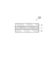
- FIG. 2 is a schematic cross-sectional view showing an embodiment of the adhesive sheet.
- the adhesive sheet 100 shown in FIG. 2 includes a base material 2 and a film adhesive 1 provided on the base material 2.
- FIG. 3 is a schematic cross-sectional view showing another embodiment of the adhesive sheet.
- the adhesive sheet 110 shown in FIG. 3 includes a base material 2, a film adhesive 1 provided on the base material 2, and a cover film provided on the surface of the film adhesive 1 opposite to the base material 2. 3 and 3.
- the base material 2 is not particularly limited, but may be a base material film.
- the base film may be similar to the support film described above.
- the cover film 3 is used to prevent damage or contamination of the film adhesive, and may be, for example, a polyethylene film, a polypropylene film, a surface release agent treated film, or the like.
- the thickness of the cover film 3 may be, for example, 15 to 200 ⁇ m or 70 to 170 ⁇ m.
- the adhesive sheets 100 and 110 can be formed by applying an adhesive composition to a base film, similar to the method of forming the film adhesive described above.
- the method of applying the adhesive composition to the substrate 2 may be the same as the method of applying the adhesive composition to the support film.
- the adhesive sheet 110 can be obtained by further laminating the cover film 3 on the film adhesive 1.
- the adhesive sheets 100 and 110 may be formed by using a film-shaped adhesive agent prepared in advance.
- the adhesive sheet 100 can be formed by laminating under a predetermined condition (for example, room temperature (20° C.) or a heated state) using a roll laminator, a vacuum laminator, or the like. Since the adhesive sheet 100 can be continuously manufactured and is excellent in efficiency, it may be formed using a roll laminator in a heated state.
- the adhesive sheet is a dicing/die bonding integrated adhesive sheet in which the base material 2 is a dicing tape.
- the process of laminating on the semiconductor wafer is performed once, so that the work efficiency can be improved.
- the dicing tape examples include plastic films such as polytetrafluoroethylene film, polyethylene terephthalate film, polyethylene film, polypropylene film, polymethylpentene film and polyimide film. Further, the dicing tape may be subjected to surface treatment such as primer coating, UV treatment, corona discharge treatment, polishing treatment and etching treatment, if necessary.
- the dicing tape may have adhesiveness. Such a dicing tape may be one in which the above-mentioned plastic film is provided with adhesiveness, or one in which the above-mentioned plastic film is provided with an adhesive layer.
- the pressure-sensitive adhesive layer may be either a pressure-sensitive type or a radiation-curable type, has a sufficient adhesive force so that the semiconductor element does not scatter during dicing, and does not damage the semiconductor element in the subsequent semiconductor element pickup step.
- a pressure-sensitive type or a radiation-curable type
- has a sufficient adhesive force so that the semiconductor element does not scatter during dicing, and does not damage the semiconductor element in the subsequent semiconductor element pickup step.
- the thickness of the dicing tape may be 60 to 150 ⁇ m or 70 to 130 ⁇ m from the viewpoints of economy and handleability of the film.
- FIG. 4 is a schematic cross-sectional view showing another embodiment of the adhesive sheet.
- FIG. 5 is a schematic cross-sectional view showing another embodiment of the adhesive sheet.
- the adhesive sheet 120 shown in FIG. 4 includes the dicing tape 7, the pressure-sensitive adhesive layer 6, and the film adhesive 1 in this order.
- the adhesive sheet 130 shown in FIG. 5 includes the dicing tape 7 and the film adhesive 1 provided on the dicing tape 7.
- the adhesive sheet 120 can be obtained, for example, by providing the pressure-sensitive adhesive layer 6 on the dicing tape 7 and further laminating the film adhesive 1 on the pressure-sensitive adhesive layer 6.
- the adhesive sheet 130 can be obtained, for example, by bonding the dicing tape 7 and the film adhesive 1 together.
- the film-like adhesive and the adhesive sheet may be used for manufacturing a semiconductor device, and the film-like adhesive and the dicing tape are applied to a semiconductor wafer or a semiconductor element (semiconductor chip) which has already been diced at 0° C. After pasting at ⁇ 90°C, the film-shaped adhesive-attached semiconductor element is obtained by cutting with a rotary blade, laser or stretching, and then the film-shaped adhesive-attached semiconductor element is applied to an organic substrate, a lead frame, or another semiconductor. It may be used for manufacturing a semiconductor device including a step of adhering on an element.
- semiconductor wafers include single crystal silicon, polycrystalline silicon, various ceramics, and compound semiconductors such as gallium arsenide.
- the film adhesive and the adhesive sheet include semiconductor elements such as IC and LSI, lead frames such as 42 alloy lead frame and copper lead frame; plastic films such as polyimide resin and epoxy resin; It can be used as an adhesive for die bonding for bonding a material impregnated and cured with a plastic such as an epoxy resin; a semiconductor mounting support member such as ceramics such as alumina.
- the film adhesive and the adhesive sheet are also suitably used as an adhesive for adhering semiconductor elements to each other in a Stacked-PKG having a structure in which a plurality of semiconductor elements are stacked.
- one semiconductor element serves as a support member on which the semiconductor element is mounted.
- the film adhesive and the adhesive sheet are, for example, a protective sheet for protecting the back surface of the semiconductor element of the flip-chip type semiconductor device, and a material for sealing between the surface of the semiconductor element of the flip-chip type semiconductor device and the adherend. It can also be used as a sealing sheet or the like.
- a semiconductor device manufactured using a film adhesive will be specifically described with reference to the drawings.
- semiconductor devices having various structures have been proposed, and the application of the film adhesive according to the present embodiment is not limited to the semiconductor device having the structure described below.
- FIG. 6 is a schematic sectional view showing an embodiment of a semiconductor device.
- the semiconductor device 200 shown in FIG. 6 is provided between the semiconductor element 9, the support member 10 on which the semiconductor element 9 is mounted, and the semiconductor element 9 and the support member 10, and is bonded to bond the semiconductor element 9 and the support member 10. And a member (cured product 1c of film adhesive).
- a connection terminal (not shown) of the semiconductor element 9 is electrically connected to an external connection terminal (not shown) via a wire 11 and sealed by a sealing material 12.
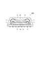
- FIG. 7 is a schematic cross-sectional view showing another embodiment of the semiconductor device.
- the first-stage semiconductor element 9a is bonded to the support member 10 on which the terminal 13 is formed by an adhesive member (cured material 1c of film adhesive), and the first-stage semiconductor element 9a.
- the semiconductor element 9b of the second stage is further adhered to the top by an adhesive member (cured product 1c of film adhesive).
- the connection terminals (not shown) of the semiconductor element 9 a in the first stage and the semiconductor element 9 b in the second stage are electrically connected to the external connection terminals via the wires 11 and sealed by the sealing material 12.
- the film adhesive according to the present embodiment can be suitably used for a semiconductor device having a structure in which a plurality of semiconductor elements are stacked.
- the semiconductor device (semiconductor package) shown in FIGS. 6 and 7 has, for example, a film adhesive interposed between a semiconductor element and a support member or between semiconductor elements and heated and pressure-bonded to each other. Are bonded, and then, if necessary, a wire bonding step, a sealing step with a sealing material, a heating and melting step including reflow with solder, and the like.
- the heating temperature in the thermocompression bonding step is usually 20 to 250° C.
- the load is usually 0.1 to 200 N
- the heating time is usually 0.1 to 300 seconds.
- the supporting member or It may be a method of attaching to a semiconductor element.
- the support member may include a member made of copper.
- a member made of copper is used as a constituent member of the semiconductor device. However, it is possible to reduce the influence of copper ions generated from the member, and it is possible to sufficiently suppress the occurrence of electrical defects due to copper ions.
- the member made of copper for example, a lead frame, a wiring, a wire, a heat dissipating material, etc. can be mentioned, but even if copper is used for any member, the influence of copper ions can be reduced. Is.
- the method of manufacturing a semiconductor device using the dicing/die-bonding integrated adhesive sheet is not limited to the method of manufacturing a semiconductor device described below.
- a semiconductor wafer is pressure-bonded to the film-like adhesive 1 on the adhesive sheet 120 (adhesive sheet with integrated dicing and die bonding), and the adhesive is held and fixed (mounting step).
- This step may be performed while pressing with a pressing means such as a pressure roll.
- the semiconductor wafer is diced.
- the semiconductor wafer is cut into a predetermined size, and a plurality of individual semiconductor elements (semiconductor chips) with a film-like adhesive are manufactured.
- the dicing can be performed, for example, from the circuit surface side of the semiconductor wafer according to a conventional method.
- a cutting method called full-cut in which even dicing tape is cut, a method in which a semiconductor wafer is cut into half and cut by cooling and pulling, a laser cutting method, and the like can be adopted.
- the dicing device used in this step is not particularly limited, and a conventionally known device can be used.
- the pickup method is not particularly limited, and various conventionally known methods can be adopted. For example, there is a method of pushing up individual semiconductor elements from the side of the dicing/die-bonding integrated adhesive sheet with a needle and picking up the pushed semiconductor elements with a pickup device.
- the pressure-sensitive adhesive layer is a radiation (for example, ultraviolet ray) curable type
- pick up is performed after irradiating the pressure-sensitive adhesive layer with radiation.
- the adhesive strength of the pressure-sensitive adhesive layer to the film adhesive is reduced, and the semiconductor element can be easily peeled off. As a result, the pickup can be performed without damaging the semiconductor element.
- the semiconductor element with a film adhesive formed by dicing is adhered to a supporting member for mounting the semiconductor element via the film adhesive.
- Bonding may be done by crimping.
- the conditions for die bonding are not particularly limited, and can be set appropriately as needed. Specifically, for example, the die bonding temperature may be 80 to 160° C., the bonding load may be 5 to 15 N, and the bonding time may be 1 to 10 seconds.
- thermosetting the film adhesive may be provided.
- thermosetting the film adhesive that bonds the support member and the semiconductor element in the bonding step it is possible to more firmly bond and fix.
- pressure may be applied simultaneously to cure.
- the heating temperature in this step can be appropriately changed depending on the constituents of the film adhesive.
- the heating temperature may be, for example, 60 to 200°C.
- the temperature or pressure may be changed stepwise.
- a wire bonding process of electrically connecting the tip of the terminal portion (inner lead) of the support member and the electrode pad on the semiconductor element with a bonding wire is performed.
- the bonding wire for example, a gold wire, an aluminum wire, a copper wire or the like is used.
- the temperature for wire bonding may be in the range of 80 to 250°C or 80 to 220°C.
- the heating time may be several seconds to several minutes.
- the wire connection may be performed by using the vibration energy of ultrasonic waves and the compression energy of applied pressure in a state of being heated within the above temperature range.
- a sealing process is performed to seal the semiconductor element with the sealing resin.
- This step is performed to protect the semiconductor element or the bonding wire mounted on the support member.
- This step is performed by molding the resin for sealing with a mold.
- the sealing resin may be, for example, an epoxy resin. The substrate and the residue are embedded by heat and pressure at the time of sealing, and peeling due to bubbles at the adhesive interface can be prevented.
- the sealing resin that is insufficiently cured in the sealing process is completely cured. Even if the film adhesive is not cured by heat in the sealing step, the film adhesive can be cured by heat as well as the curing of the sealing resin in this step, so that the adhesive fixation can be achieved.
- the heating temperature in this step can be appropriately set depending on the type of sealing resin, and may be, for example, in the range of 165 to 185° C., and the heating time may be about 0.5 to 8 hours.
- the semiconductor element with the film adhesive adhered to the support member is heated using a reflow oven.
- a resin-sealed semiconductor device may be surface-mounted on the support member.
- the surface mounting method include reflow soldering in which solder is supplied in advance on a printed wiring board and then heated and melted by hot air or the like for soldering.
- the heating method include hot air reflow and infrared reflow.
- the heating method may be a method of heating the whole or a method of heating a local portion.
- the heating temperature may be, for example, in the range of 240 to 280°C.
- the film adhesive according to the present embodiment tends to have a lower cohesive force and an improved embedding property by using a specific acrylic rubber. Therefore, it is difficult for air bubbles to be caught in the semiconductor device, the air bubbles can be easily diffused in the sealing step, and peeling due to the air bubbles at the adhesive interface can be prevented.
- Thermosetting resin component (A1) Thermosetting resin (A1-1) YDCN-700-10 (trade name, Nippon Steel & Sumikin Chemical Co., Ltd., o-cresol novolac type epoxy resin, epoxy equivalent: 209 g/eq) )
- Curing agent (A2-1) PSM4326 (trade name, manufactured by Gunei Chemical Industry Co., Ltd., phenol novolac resin, hydroxyl equivalent: 105 g/eq)
- A3 Elastomer (A3-1) SG-P3 (trade name, manufactured by Nagase Chemtex Co., Ltd., methyl ethyl ketone solution of acrylic rubber having an epoxy group, weight average molecular weight of acrylic rubber: 850,000)
- B Leveling agent (B1) BYK-333 (trade name, manufactured by BYK Japan KK, polyether-modified polydimethylsiloxane)
- C Inorganic filler (C1) SC2050-HLG (trade name, manufactured by Admatechs Co., Ltd., silica filler dispersion, average particle size 0.50 ⁇ m)
- the produced adhesive varnish was filtered with a 100-mesh filter and vacuum degassed.
- a polyethylene terephthalate (PET) film having a thickness of 38 ⁇ m and subjected to a mold release treatment was prepared, and the adhesive varnish after vacuum defoaming was applied onto the PET film.
- the applied adhesive varnish was heated and dried in two stages of 90° C. for 5 minutes and 130° C. for 5 minutes to obtain film adhesives of Examples 1 to 3 and Comparative Example 1 in the B stage state. ..
- the film adhesive was adjusted to have a thickness of 10 ⁇ m depending on the coating amount of the adhesive varnish.
- NMP N-methyl-2-pyrrolidone
- the film adhesives of Examples 1 to 3 and Comparative Example 1 in the B stage state are further dried by heating at 170° C. for 1 hour, and the film adhesives of Examples 1 to 3 and Comparative Example 1 in the C stage state.
- the film adhesives (thickness: 10 ⁇ m) of Examples 1 to 3 and Comparative Example 1 in the C stage state were each cut out into a circle with a diameter of about 3 cm.
- two silicon packing sheets having a thickness of 1.5 mm, an outer diameter of about 3 cm and an inner diameter of 1.8 cm were prepared.
- the film adhesive cut out in a circular shape was sandwiched between two silicon packing sheets, sandwiched between the flange portions of two glass cells having a volume of 50 mL, and fixed with a rubber band.
- a dicing tape manufactured by Hitachi Chemical Co., Ltd., thickness: 110 ⁇ m
- the film adhesives thickness: 10 ⁇ m
- An adhesive dicing-die bonding type integrated adhesive sheet containing a chemical was prepared.
- a semiconductor wafer having a thickness of 400 ⁇ m was laminated on the film adhesive side of the dicing-die bonding integral type adhesive sheet at a stage temperature of 70° C. to prepare a dicing sample.
- the obtained dicing sample was cut using a full-auto dicer DFD-6361 (manufactured by Disco Corporation).
- the cutting was performed by a step cut method using two blades, and a dicing blade ZH05-SD3500-N1-xx-DD and ZH05-SD4000-N1-xx-BB (both manufactured by Disco Corporation) were used.
- the cutting conditions were a blade rotation speed of 4000 rpm, a cutting speed of 50 mm/sec, and a chip size of 5 mm ⁇ 5 mm.
- the cutting was performed in the first step so that the semiconductor wafer remained about 200 ⁇ m, and then in the second step so that the dicing tape had a cut of about 20 ⁇ m.
- the semiconductor chip obtained by cutting was thermocompression bonded onto a solder resist (Taiyo Holdings Co., Ltd., trade name: AUS-308).
- the pressure bonding conditions were a temperature of 120° C., a time of 1 second, and a pressure of 0.1 MPa.
- the sample obtained by pressure bonding was put into a dryer and cured at 170° C. for 1 hour.
- the universal bond tester Nedson Advance Technology Co., Ltd., product name: Series 4000
- the strength was measured.
- the measurement conditions were a stage temperature of 250°C. The results are shown in Table 1.
- the film adhesives of Examples 1 to 3 were less likely to penetrate copper ions than the film adhesives of Comparative Example 1. It is presumed that this is because the leveling agent lowers the surface tension of the adhesive and suppresses the uptake of copper ions in the surface layer of the adhesive.
- the film-like adhesive of the present invention can sufficiently suppress the problems caused by the movement of copper ions in the adhesive.
Landscapes
- Chemical & Material Sciences (AREA)
- Organic Chemistry (AREA)
- Adhesives Or Adhesive Processes (AREA)
- Adhesive Tapes (AREA)
- Dicing (AREA)
- Die Bonding (AREA)
Abstract
Description
(A1)成分は、接着性の観点から、エポキシ樹脂であってよい。エポキシ樹脂は、分子内にエポキシ基を有するものであれば、特に制限なく用いることができる。エポキシ樹脂としては、例えば、ビスフェノールA型エポキシ樹脂、ビスフェノールF型エポキシ樹脂、ビスフェノールS型エポキシ樹脂、フェノールノボラック型エポキシ樹脂、クレゾールノボラック型エポキシ樹脂、ビスフェノールAノボラック型エポキシ樹脂、ビスフェノールFノボラック型エポキシ樹脂、スチルベン型エポキシ樹脂、トリアジン骨格含有エポキシ樹脂、フルオレン骨格含有エポキシ樹脂、トリフェノールメタン型エポキシ樹脂、ビフェニル型エポキシ樹脂、キシリレン型エポキシ樹脂、ビフェニルアラルキル型エポキシ樹脂、ナフタレン型エポキシ樹脂、多官能フェノール類、アントラセン等の多環芳香族類のジグリシジルエーテル化合物などが挙げられる。これらは、1種を単独で又は2種以上を組み合わせて用いてもよい。これらの中でも、(A1)成分は、フィルムのタック性、柔軟性などの観点から、クレゾールノボラック型エポキシ樹脂、フェノールノボラック型エポキシ樹脂、ビスフェノールF型エポキシ樹脂、又はビスフェノールA型エポキシ樹脂であってもよい。
(A2)成分は、エポキシ樹脂の硬化剤となり得るフェノール樹脂であってよい。フェノール樹脂は、分子内にフェノール性水酸基を有するものであれば特に制限なく用いることができる。フェノール樹脂としては、例えば、フェノール、クレゾール、レゾルシン、カテコール、ビスフェノールA、ビスフェノールF、フェニルフェノール、アミノフェノール等のフェノール類及び/又はα-ナフトール、β-ナフトール、ジヒドロキシナフタレン等のナフトール類とホルムアルデヒド等のアルデヒド基を有する化合物とを酸性触媒下で縮合又は共縮合させて得られるノボラック型フェノール樹脂、アリル化ビスフェノールA、アリル化ビスフェノールF、アリル化ナフタレンジオール、フェノールノボラック、フェノール等のフェノール類及び/又はナフトール類とジメトキシパラキシレン又はビス(メトキシメチル)ビフェニルから合成されるフェノールアラルキル樹脂、ナフトールアラルキル樹脂などが挙げられる。これらは、1種を単独で又は2種以上を組み合わせて用いてもよい。これらの中でも、フェノール樹脂は、フェノール樹脂は、フェノールノボラック型フェノール樹脂又はナフトールアラルキル樹脂であってもよい。
(A3)成分は、(メタ)アクリル酸エステルに由来する構成単位を主成分として有するアクリルゴムであってよい。(A3)成分における(メタ)アクリル酸エステルに由来する構成単位の含有量は、構成単位全量を基準として、例えば、70質量%以上、80質量%以上、又は90質量%以上であってよい。アクリルゴムは、エポキシ基、アルコール性又はフェノール性水酸基、カルボキシル基等の架橋性官能基を有する(メタ)アクリル酸エステルに由来する構成単位を含むものであってよい。
フィルム状接着剤が(B)成分を含有することによって、接着剤表層の銅イオンの取り込みを抑制することができる。(B)成分は、フィルム状接着剤の表面張力を調整することができるのであれば特に制限されないが、シロキサン構造を有する化合物(言い換えると、ポリシロキサン又はシリコーン)であってよい。このような(B)成分としては、例えば、ポリエーテル変性、ポリエステル変性、アラルキル変性、フェニル変性等のポリシロキサン(シリコーン)などが挙げられる。これらは、1種を単独で又は2種以上を組み合わせて用いてもよい。
(C)成分としては、例えば、水酸化アルミニウム、水酸化マグネシウム、炭酸カルシウム、炭酸マグネシウム、ケイ酸カルシウム、ケイ酸マグネシウム、酸化カルシウム、酸化マグネシウム、酸化アルミニウム、窒化アルミニウム、ホウ酸アルミウィスカ、窒化ホウ素、シリカ等が挙げられる。これらは、1種を単独で又は2種以上を組み合わせて用いてもよい。これらの中でも、(C)成分は、溶融粘度の調整の観点から、シリカであってもよい。(C)成分の形状は、特に制限されないが、球状であってよい。
(D)成分は、シランカップリング剤であってよい。シランカップリング剤としては、例えば、γ-ウレイドプロピルトリエトキシシラン、γ-メルカプトプロピルトリメトキシシラン、3-フェニルアミノプロピルトリメトキシシラン、3-(2-アミノエチル)アミノプロピルトリメトキシシラン等が挙げられる。これらは、1種を単独で又は2種以上を組み合わせて用いてもよい。
(E)成分は、特に限定されず、一般に使用されるものを用いることができる。(E)成分としては、例えば、イミダゾール類及びその誘導体、有機リン系化合物、第二級アミン類、第三級アミン類、第四級アンモニウム塩等が挙げられる。これらは、1種を単独で又は2種以上を組み合わせて用いてもよい。これらの中でも、反応性の観点から(E)成分は、イミダゾール類及びその誘導体であってよい。
(実施例1~3及び比較例1)
<接着剤ワニスの調製>
表1に示す品名及び組成比(単位:質量部)で、(A1)熱硬化性樹脂としてのエポキシ樹脂、(A2)硬化剤としてのフェノール樹脂、及び(C)無機フィラーからなる組成物にシクロヘキサノンを加え、撹拌混合した。これに、表1に示す(A3)エラストマとしてのアクリルゴムを加えて撹拌し、さらに表1に示す(D)カップリング剤、(E)硬化促進剤、及び(B)レベリング剤を加えて、各成分が均一になるまで撹拌して、接着剤ワニスを調製した。なお、表1に示す(A3)成分及び(C)成分の数値は、固形分の質量部を意味する。
(A1)熱硬化性樹脂
(A1-1)YDCN-700-10(商品名、新日鉄住金化学株式会社製、o-クレゾールノボラック型エポキシ樹脂、エポキシ当量:209g/eq)
(A2)硬化剤
(A2-1)PSM4326(商品名、群栄化学工業株式会社製、フェノールノボラック樹脂、水酸基当量:105g/eq)
(A3)エラストマ
(A3-1)SG-P3(商品名、ナガセケムテックス株式会社製、エポキシ基を有するアクリルゴムのメチルエチルケトン溶液、アクリルゴムの重量平均分子量:85万)
(B1)BYK-333(商品名、ビックケミー・ジャパン株式会社製、ポリエーテル変性ポリジメチルシロキサン)
(C1)SC2050-HLG(商品名、アドマテックス株式会社製、シリカフィラー分散液、平均粒径0.50μm)
(D1)A-189(商品名、日本ユニカー株式会社製、γ-メルカプトプロピルトリメトキシシラン)
(D2)A-1160(商品名、日本ユニカー株式会社製、γ-ウレイドプロピルトリエトキシシラン)
(E1)2PZ-CN(商品名、四国化成工業株式会社製、1-シアノエチル-2-フェニルイミダゾール)
作製した接着剤ワニスを100メッシュのフィルターでろ過し、真空脱泡した。基材フィルムとして、厚み38μmの離型処理を施したポリエチレンテレフタレート(PET)フィルムを用意し、真空脱泡後の接着剤ワニスをPETフィルム上に塗布した。塗布した接着剤ワニスを、90℃で5分間、続いて130℃で5分間の2段階で加熱乾燥し、Bステージ状態にある実施例1~3及び比較例1のフィルム状接着剤を得た。フィルム状接着剤においては、接着剤ワニスの塗布量によって、厚み10μmになるように調整した。
<A液の調製>
無水硫酸銅(II)2.0gを蒸留水1020gに溶解させ、完全に硫酸銅が溶解するまで撹拌し、銅イオン濃度がCu元素換算で濃度500mg/kgである硫酸銅水溶液を調製した。得られた硫酸銅水溶液をA液とした。
無水硫酸ナトリウム1.0gを蒸留水1000gに溶解させ、完全に硫酸ナトリウムが溶解するまで撹拌した。これにさらにN-メチル-2-ピロリドン(NMP)を1000g加え、撹拌した。その後、室温になるまで空冷して硫酸ナトリウム水溶液を得た。得られた溶液をB液とした。
Bステージ状態にある実施例1~3及び比較例1のフィルム状接着剤をさらに170℃、1時間で加熱乾燥し、Cステージ状態にある実施例1~3及び比較例1のフィルム状接着剤を作製した。Cステージ状態にある実施例1~3及び比較例1のフィルム状接着剤(厚み:10μm)を、それぞれ直径約3cmの円状に切り抜いた。次に、厚み1.5mm、外径約3cm、内径1.8cmのシリコンパッキンシートを2枚用意した。円状に切り抜いたフィルム状接着剤を2枚のシリコンパッキンシートで挟み、これを容積50mLの2つのガラス製セルのフランジ部で挟み、ゴムバンドで固定した。
<半導体装置の作製>
ダイシングテープ(日立化成株式会社製、厚み110μm)を用意し、Bステージ状態にある実施例1~3及び比較例1のフィルム状接着剤(厚み10μm)を貼り付けて、ダイシングテープ及びフィルム状接着剤を備えるダイシング-ダイボンディング一体型接着シートを作製した。ダイシング-ダイボンディング一体型接着シートのフィルム状接着剤側に400μm厚の半導体ウェハを、ステージ温度70℃でラミネートし、ダイシングサンプルを作製した。

Claims (11)
- 半導体素子と前記半導体素子を搭載する支持部材とを接着するためのフィルム状接着剤であって、
前記フィルム状接着剤が、熱硬化性樹脂成分と、レベリング剤とを含有する、フィルム状接着剤。 - 前記レベリング剤が、シロキサン構造を有する化合物である、請求項1に記載のフィルム状接着剤。
- 前記熱硬化性樹脂成分が、熱硬化性樹脂と、硬化剤と、エラストマとを含む、請求項1又は2に記載のフィルム状接着剤。
- 前記フィルム状接着剤の厚みが、50μm以下である、請求項1~3のいずれか一項に記載のフィルム状接着剤。
- 基材と、
前記基材の一方の面上に設けられた請求項1~4のいずれか一項に記載のフィルム状接着剤と、
を備える、接着シート。 - 前記基材が、ダイシングテープである、請求項5に記載の接着シート。
- 半導体素子と、
前記半導体素子を搭載する支持部材と、
前記半導体素子及び前記支持部材の間に設けられ、前記半導体素子と前記支持部材とを接着する接着部材と、
を備え、
前記接着部材が、請求項1~4のいずれか一項に記載のフィルム状接着剤の硬化物である、半導体装置。 - 前記支持部材が、銅を素材とする部材を含む、請求項7に記載の半導体装置。
- 請求項1~4のいずれか一項に記載のフィルム状接着剤を用いて、半導体素子と支持部材とを接着する工程を備える、半導体装置の製造方法。
- 半導体ウェハに、請求項5又は6に記載の接着シートの前記フィルム状接着剤を貼り付ける工程と、
前記フィルム状接着剤を貼り付けた前記半導体ウェハを切断することによって、複数の個片化されたフィルム状接着剤付き半導体素子を作製する工程と、
前記フィルム状接着剤付き半導体素子を支持部材に接着する工程と、
を備える、半導体装置の製造方法。 - 前記支持部材に接着された前記フィルム状接着剤付き半導体素子に対して、リフロー炉を用いて加熱する工程をさらに備える、請求項10に記載の半導体装置の製造方法。
Priority Applications (3)
| Application Number | Priority Date | Filing Date | Title |
|---|---|---|---|
| SG11202108023SA SG11202108023SA (en) | 2019-01-28 | 2020-01-20 | Filmy adhesive, adhesive sheet, semiconductor device, and method for manufacturing same |
| KR1020217024426A KR102693643B1 (ko) | 2019-01-28 | 2020-01-20 | 필름상 접착제, 접착 시트, 및 반도체 장치 및 그 제조 방법 |
| CN202080011016.6A CN113348539A (zh) | 2019-01-28 | 2020-01-20 | 膜状黏合剂、黏合片以及半导体装置及其制造方法 |
Applications Claiming Priority (2)
| Application Number | Priority Date | Filing Date | Title |
|---|---|---|---|
| JP2019-012270 | 2019-01-28 | ||
| JP2019012270A JP7251167B2 (ja) | 2019-01-28 | 2019-01-28 | フィルム状接着剤、接着シート、並びに半導体装置及びその製造方法 |
Publications (1)
| Publication Number | Publication Date |
|---|---|
| WO2020158490A1 true WO2020158490A1 (ja) | 2020-08-06 |
Family
ID=71842082
Family Applications (1)
| Application Number | Title | Priority Date | Filing Date |
|---|---|---|---|
| PCT/JP2020/001788 Ceased WO2020158490A1 (ja) | 2019-01-28 | 2020-01-20 | フィルム状接着剤、接着シート、並びに半導体装置及びその製造方法 |
Country Status (6)
| Country | Link |
|---|---|
| JP (1) | JP7251167B2 (ja) |
| KR (1) | KR102693643B1 (ja) |
| CN (1) | CN113348539A (ja) |
| SG (1) | SG11202108023SA (ja) |
| TW (1) | TWI830861B (ja) |
| WO (1) | WO2020158490A1 (ja) |
Families Citing this family (1)
| Publication number | Priority date | Publication date | Assignee | Title |
|---|---|---|---|---|
| KR102466644B1 (ko) * | 2021-03-23 | 2022-11-16 | 주식회사 엘엠에스 | 점착제 조성물 및 광학 점착제 |
Citations (5)
| Publication number | Priority date | Publication date | Assignee | Title |
|---|---|---|---|---|
| JP2005307037A (ja) * | 2004-04-22 | 2005-11-04 | Nagase Chemtex Corp | フィルム状エポキシ樹脂組成物 |
| JP2011052109A (ja) * | 2009-09-01 | 2011-03-17 | Hitachi Chem Co Ltd | フィルム状接着剤、接着シート及び半導体装置 |
| JP2012158631A (ja) * | 2011-01-31 | 2012-08-23 | Shin-Etsu Chemical Co Ltd | エポキシ樹脂組成物、それを用いたダイアタッチ方法及び該組成物の硬化物を有する半導体装置 |
| JP2015081269A (ja) * | 2013-10-21 | 2015-04-27 | 信越化学工業株式会社 | スクリーン印刷用導電性エポキシ樹脂組成物、それを用いたダイアタッチ方法および該組成物の硬化物を有する半導体装置 |
| JP2017105883A (ja) * | 2015-12-07 | 2017-06-15 | 信越化学工業株式会社 | 液状樹脂組成物及び該組成物を用いたダイアタッチ方法、並びに該組成物の硬化物を有する半導体装置 |
Family Cites Families (9)
| Publication number | Priority date | Publication date | Assignee | Title |
|---|---|---|---|---|
| JP5087910B2 (ja) | 2005-12-13 | 2012-12-05 | 東レ株式会社 | 電子機器用接着剤組成物、電子機器用接着剤シートおよびそれを用いた電子部品 |
| JP2009111340A (ja) * | 2007-10-11 | 2009-05-21 | Hitachi Chem Co Ltd | 接着剤付きウエハ、接着剤組成物及び接着剤付きウエハの製造方法 |
| JP5804820B2 (ja) | 2011-07-25 | 2015-11-04 | 日東電工株式会社 | 半導体装置製造用の接着シート、半導体装置製造用の接着シートを有する半導体装置、及び、半導体装置の製造方法 |
| WO2014065136A1 (ja) * | 2012-10-22 | 2014-05-01 | 三菱レイヨン株式会社 | 積層構造体およびその製造方法と、物品 |
| KR102343970B1 (ko) | 2015-01-14 | 2021-12-27 | 린텍 가부시키가이샤 | 수지막 형성용 시트, 수지막 형성용 복합 시트 및 실리콘 웨이퍼의 재생 방법 |
| JP2016190964A (ja) * | 2015-03-31 | 2016-11-10 | 日立化成株式会社 | 接着フィルム |
| WO2017038916A1 (ja) * | 2015-09-01 | 2017-03-09 | リンテック株式会社 | 粘着シート |
| JP6521823B2 (ja) | 2015-10-01 | 2019-05-29 | リンテック株式会社 | ダイシングダイボンディングシート |
| US11624009B2 (en) * | 2016-12-22 | 2023-04-11 | Toagosei Co., Ltd. | Adhesive composition, and coverlay film, bonding sheet, copper-clad laminate and electromagnetic shielding material, each using said adhesive composition |
-
2019
- 2019-01-28 JP JP2019012270A patent/JP7251167B2/ja active Active
-
2020
- 2020-01-20 KR KR1020217024426A patent/KR102693643B1/ko active Active
- 2020-01-20 CN CN202080011016.6A patent/CN113348539A/zh active Pending
- 2020-01-20 SG SG11202108023SA patent/SG11202108023SA/en unknown
- 2020-01-20 WO PCT/JP2020/001788 patent/WO2020158490A1/ja not_active Ceased
- 2020-01-21 TW TW109102299A patent/TWI830861B/zh active
Patent Citations (5)
| Publication number | Priority date | Publication date | Assignee | Title |
|---|---|---|---|---|
| JP2005307037A (ja) * | 2004-04-22 | 2005-11-04 | Nagase Chemtex Corp | フィルム状エポキシ樹脂組成物 |
| JP2011052109A (ja) * | 2009-09-01 | 2011-03-17 | Hitachi Chem Co Ltd | フィルム状接着剤、接着シート及び半導体装置 |
| JP2012158631A (ja) * | 2011-01-31 | 2012-08-23 | Shin-Etsu Chemical Co Ltd | エポキシ樹脂組成物、それを用いたダイアタッチ方法及び該組成物の硬化物を有する半導体装置 |
| JP2015081269A (ja) * | 2013-10-21 | 2015-04-27 | 信越化学工業株式会社 | スクリーン印刷用導電性エポキシ樹脂組成物、それを用いたダイアタッチ方法および該組成物の硬化物を有する半導体装置 |
| JP2017105883A (ja) * | 2015-12-07 | 2017-06-15 | 信越化学工業株式会社 | 液状樹脂組成物及び該組成物を用いたダイアタッチ方法、並びに該組成物の硬化物を有する半導体装置 |
Also Published As
| Publication number | Publication date |
|---|---|
| CN113348539A (zh) | 2021-09-03 |
| SG11202108023SA (en) | 2021-08-30 |
| TWI830861B (zh) | 2024-02-01 |
| TW202037696A (zh) | 2020-10-16 |
| KR20210114010A (ko) | 2021-09-17 |
| KR102693643B1 (ko) | 2024-08-09 |
| JP7251167B2 (ja) | 2023-04-04 |
| JP2020120073A (ja) | 2020-08-06 |
Similar Documents
| Publication | Publication Date | Title |
|---|---|---|
| JPWO2019220540A1 (ja) | 半導体装置、並びに、その製造に使用する熱硬化性樹脂組成物及びダイシングダイボンディング一体型テープ | |
| JP7655362B2 (ja) | 半導体装置 | |
| KR20230129992A (ko) | 필름상 접착제, 다이싱·다이본딩 일체형 필름, 및 반도체장치 및 그 제조 방법 | |
| JP7255146B2 (ja) | フィルム状接着剤、接着シート、並びに半導体装置及びその製造方法 | |
| KR20240148336A (ko) | 필름상 접착제, 다이싱·다이본딩 일체형 필름, 및 반도체 장치 및 그 제조 방법 | |
| JP2025107273A (ja) | フィルム状接着剤、接着シート、並びに半導体装置及びその製造方法 | |
| WO2020129996A1 (ja) | フィルム状接着剤、接着シート、並びに半導体装置及びその製造方法 | |
| WO2025084363A1 (ja) | フィルム状接着剤、ダイシング・ダイボンディング一体型フィルム、並びに半導体装置及びその製造方法 | |
| KR102693643B1 (ko) | 필름상 접착제, 접착 시트, 및 반도체 장치 및 그 제조 방법 | |
| JP7435458B2 (ja) | フィルム状接着剤、接着シート、並びに半導体装置及びその製造方法 | |
| KR20250162579A (ko) | 필름상 접착제, 다이싱·다이본딩 일체형 필름, 및 반도체 장치 및 그 제조 방법 | |
| WO2020065783A1 (ja) | フィルム状接着剤、接着シート、並びに半導体装置及びその製造方法 | |
| JP2022044991A (ja) | ダイボンディングフィルム、接着シート、並びに半導体装置及びその製造方法 | |
| WO2022149581A1 (ja) | 接着剤組成物、フィルム状接着剤、ダイシング・ダイボンディング一体型フィルム、並びに半導体装置及びその製造方法 | |
| KR20240090161A (ko) | 필름상 접착제, 다이싱·다이본딩 일체형 필름, 및 반도체 장치 및 그 제조 방법 |
Legal Events
| Date | Code | Title | Description |
|---|---|---|---|
| 121 | Ep: the epo has been informed by wipo that ep was designated in this application |
Ref document number: 20749769 Country of ref document: EP Kind code of ref document: A1 |
|
| NENP | Non-entry into the national phase |
Ref country code: DE |
|
| ENP | Entry into the national phase |
Ref document number: 20217024426 Country of ref document: KR Kind code of ref document: A |
|
| 32PN | Ep: public notification in the ep bulletin as address of the adressee cannot be established |
Free format text: NOTING OF LOSS OF RIGHTS PURSUANT TO RULE 112(1) EPC (EPO FORM 1205A DATED 22.10.2021) |
|
| 122 | Ep: pct application non-entry in european phase |
Ref document number: 20749769 Country of ref document: EP Kind code of ref document: A1 |