WO2020158041A1 - 積層体および電子素子 - Google Patents
積層体および電子素子 Download PDFInfo
- Publication number
- WO2020158041A1 WO2020158041A1 PCT/JP2019/037057 JP2019037057W WO2020158041A1 WO 2020158041 A1 WO2020158041 A1 WO 2020158041A1 JP 2019037057 W JP2019037057 W JP 2019037057W WO 2020158041 A1 WO2020158041 A1 WO 2020158041A1
- Authority
- WO
- WIPO (PCT)
- Prior art keywords
- ions
- exposed surface
- maximum value
- sic
- depth
- Prior art date
- Legal status (The legal status is an assumption and is not a legal conclusion. Google has not performed a legal analysis and makes no representation as to the accuracy of the status listed.)
- Ceased
Links
Images





Classifications
-
- C—CHEMISTRY; METALLURGY
- C01—INORGANIC CHEMISTRY
- C01B—NON-METALLIC ELEMENTS; COMPOUNDS THEREOF; METALLOIDS OR COMPOUNDS THEREOF NOT COVERED BY SUBCLASS C01C
- C01B32/00—Carbon; Compounds thereof
- C01B32/15—Nano-sized carbon materials
- C01B32/182—Graphene
-
- C—CHEMISTRY; METALLURGY
- C01—INORGANIC CHEMISTRY
- C01B—NON-METALLIC ELEMENTS; COMPOUNDS THEREOF; METALLOIDS OR COMPOUNDS THEREOF NOT COVERED BY SUBCLASS C01C
- C01B32/00—Carbon; Compounds thereof
- C01B32/15—Nano-sized carbon materials
- C01B32/182—Graphene
- C01B32/184—Preparation
-
- B—PERFORMING OPERATIONS; TRANSPORTING
- B32—LAYERED PRODUCTS
- B32B—LAYERED PRODUCTS, i.e. PRODUCTS BUILT-UP OF STRATA OF FLAT OR NON-FLAT, e.g. CELLULAR OR HONEYCOMB, FORM
- B32B18/00—Layered products essentially comprising ceramics, e.g. refractory products
-
- B—PERFORMING OPERATIONS; TRANSPORTING
- B32—LAYERED PRODUCTS
- B32B—LAYERED PRODUCTS, i.e. PRODUCTS BUILT-UP OF STRATA OF FLAT OR NON-FLAT, e.g. CELLULAR OR HONEYCOMB, FORM
- B32B9/00—Layered products comprising a layer of a particular substance not covered by groups B32B11/00 - B32B29/00
-
- H—ELECTRICITY
- H10—SEMICONDUCTOR DEVICES; ELECTRIC SOLID-STATE DEVICES NOT OTHERWISE PROVIDED FOR
- H10D—INORGANIC ELECTRIC SEMICONDUCTOR DEVICES
- H10D30/00—Field-effect transistors [FET]
- H10D30/01—Manufacture or treatment
-
- H—ELECTRICITY
- H10—SEMICONDUCTOR DEVICES; ELECTRIC SOLID-STATE DEVICES NOT OTHERWISE PROVIDED FOR
- H10D—INORGANIC ELECTRIC SEMICONDUCTOR DEVICES
- H10D30/00—Field-effect transistors [FET]
- H10D30/40—FETs having zero-dimensional [0D], one-dimensional [1D] or two-dimensional [2D] charge carrier gas channels
- H10D30/47—FETs having zero-dimensional [0D], one-dimensional [1D] or two-dimensional [2D] charge carrier gas channels having two-dimensional [2D] charge carrier gas channels, e.g. nanoribbon FETs or high electron mobility transistors [HEMT]
-
- H—ELECTRICITY
- H10—SEMICONDUCTOR DEVICES; ELECTRIC SOLID-STATE DEVICES NOT OTHERWISE PROVIDED FOR
- H10D—INORGANIC ELECTRIC SEMICONDUCTOR DEVICES
- H10D48/00—Individual devices not covered by groups H10D1/00 - H10D44/00
- H10D48/30—Devices controlled by electric currents or voltages
- H10D48/32—Devices controlled by only the electric current supplied, or only the electric potential applied, to an electrode which does not carry the current to be rectified, amplified or switched
- H10D48/36—Unipolar devices
- H10D48/362—Unipolar transistors having ohmic electrodes on emitter-like, base-like, and collector-like regions, e.g. hot electron transistors [HET], metal base transistors [MBT], resonant tunnelling transistors [RTT], bulk barrier transistors [BBT], planar doped barrier transistors [PDBT] or charge injection transistors [CHINT]
-
- H—ELECTRICITY
- H10—SEMICONDUCTOR DEVICES; ELECTRIC SOLID-STATE DEVICES NOT OTHERWISE PROVIDED FOR
- H10D—INORGANIC ELECTRIC SEMICONDUCTOR DEVICES
- H10D62/00—Semiconductor bodies, or regions thereof, of devices having potential barriers
- H10D62/80—Semiconductor bodies, or regions thereof, of devices having potential barriers characterised by the materials
- H10D62/83—Semiconductor bodies, or regions thereof, of devices having potential barriers characterised by the materials being Group IV materials, e.g. B-doped Si or undoped Ge
- H10D62/8303—Diamond
-
- H—ELECTRICITY
- H10—SEMICONDUCTOR DEVICES; ELECTRIC SOLID-STATE DEVICES NOT OTHERWISE PROVIDED FOR
- H10D—INORGANIC ELECTRIC SEMICONDUCTOR DEVICES
- H10D62/00—Semiconductor bodies, or regions thereof, of devices having potential barriers
- H10D62/80—Semiconductor bodies, or regions thereof, of devices having potential barriers characterised by the materials
- H10D62/881—Semiconductor bodies, or regions thereof, of devices having potential barriers characterised by the materials being a two-dimensional material
- H10D62/882—Graphene
-
- C—CHEMISTRY; METALLURGY
- C01—INORGANIC CHEMISTRY
- C01B—NON-METALLIC ELEMENTS; COMPOUNDS THEREOF; METALLOIDS OR COMPOUNDS THEREOF NOT COVERED BY SUBCLASS C01C
- C01B2204/00—Structure or properties of graphene
- C01B2204/04—Specific amount of layers or specific thickness
-
- C—CHEMISTRY; METALLURGY
- C01—INORGANIC CHEMISTRY
- C01B—NON-METALLIC ELEMENTS; COMPOUNDS THEREOF; METALLOIDS OR COMPOUNDS THEREOF NOT COVERED BY SUBCLASS C01C
- C01B2204/00—Structure or properties of graphene
- C01B2204/20—Graphene characterized by its properties
- C01B2204/22—Electronic properties
Definitions
- the present disclosure relates to a laminated body and an electronic device.
- Graphene is a substance in which carbon atoms form a sp 2 hybrid orbital and are planarly bonded to each other. Due to such a bonded state of carbon atoms, the mobility of carriers (electrons) in graphene is extremely high. If graphene can be effectively used as a channel of an electronic device such as a transistor, the performance of the electronic device can be improved.
- a method has been proposed in which a substrate made of SiC (silicon carbide) is heated to release silicon atoms to convert the surface layer portion of the substrate into graphene and obtain a laminate having a graphene film formed on the surface layer portion of the substrate.
- SiC silicon carbide
- Patent Document 1 after the silicon atoms are released, the substrate is subjected to hydrogen treatment to bond hydrogen to the terminal ends of the silicon atoms located on the substrate side.
- a laminated body includes a base portion including silicon carbide, the base portion having a first main surface, and an exposed surface that is a main surface opposite to a side on which the base portion is located. And a graphene film having the same.
- the detection intensity of C 6 ions was measured from the exposed surface. It has a maximum value at a depth of more than 0 nm and 2.5 nm or less.
- the detected intensity of C 3 ions has a maximum value at a depth of more than 0 nm and 3.0 nm or less from the exposed surface.
- the detection intensity of SiC 4 ions has a maximum value at a depth of 0.5 nm or more and 5.0 nm or less from the exposed surface.
- the detection intensity of SiC ions has a maximum value at a depth of 0.5 nm or more and 10.0 nm or less from the exposed surface.
- the detection intensity of Si 2 ions has a maximum value at a depth of 0.5 nm or more and 10.0 nm or less from the exposed surface.
- the maximum value of the detected intensity of SiC 4 ions, the value the distance from the exposed surface is divided by the average value of the detected intensity of SiC 4 ions in the region is 8nm or more 12nm or less in the thickness direction of the laminate, one or more 3. It is 5 or less.
- FIG. 1 is a schematic cross-sectional view showing the structure of the laminated body according to the first embodiment.
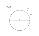
- FIG. 2 is a view of the laminated body according to the first embodiment as viewed in the thickness direction.
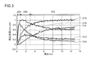
- FIG. 3 is a graph showing the results of time-of-flight secondary ion mass spectrometry of the laminate according to the first embodiment.
- FIG. 4 is a graph showing the relationship between the drain voltage and the drain current when the gate voltage is changed in the transistor manufactured using the stacked body according to the first embodiment.
- FIG. 5 is a graph showing the results of time-of-flight secondary ion mass spectrometry analysis of a laminate that is outside the scope of the present disclosure.
- FIG. 1 is a schematic cross-sectional view showing the structure of the laminated body according to the first embodiment.
- FIG. 2 is a view of the laminated body according to the first embodiment as viewed in the thickness direction.
- FIG. 3 is a graph showing the results of time-of-flight secondary ion mass
- FIG. 6 is a graph showing the relationship between the drain voltage and the drain current when the gate voltage is changed in the transistor manufactured using the laminated body having the characteristics of the time-of-flight secondary ion mass spectrometry shown in FIG. Is.
- FIG. 7 is a flowchart showing typical steps of the method for manufacturing a laminated body according to the first embodiment.
- FIG. 8 is a schematic cross-sectional view showing the method for manufacturing the laminate according to the first embodiment.
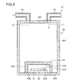
- FIG. 9 is a schematic cross-sectional view showing the structure of the heating device.
- FIG. 10 is a schematic sectional view of a field effect transistor (FET) according to the second embodiment.
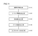
- FIG. 11 is a flowchart showing typical steps of a method for manufacturing an FET including a graphene film.
- FIG. FET field effect transistor
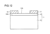
- FIG. 12 is a schematic cross-sectional view for explaining the method for manufacturing the FET including the graphene film.
- FIG. 13 is a schematic cross-sectional view for explaining the method of manufacturing the FET including the graphene film.
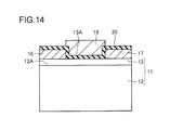
- FIG. 14 is a schematic cross-sectional view for explaining the method of manufacturing the FET including the graphene film.
- the laminated body is a base portion that includes silicon carbide and has a first main surface, and a main surface that is disposed on the first main surface and that is opposite to the side where the base portion is located. And a graphene film having an exposed surface.
- the detection intensity of C 6 ions was measured from the exposed surface.
- the detected intensity of C 3 ions has a maximum value at a depth of more than 0 nm and 3.0 nm or less from the exposed surface.
- the detection intensity of SiC 4 ions has a maximum value at a depth of 0.5 nm or more and 5.0 nm or less from the exposed surface.
- the detection intensity of SiC ions has a maximum value at a depth of 0.5 nm or more and 10.0 nm or less from the exposed surface.
- the detection intensity of Si 2 ions has a maximum value at a depth of 0.5 nm or more and 10.0 nm or less from the exposed surface.
- the maximum value of the detected intensity of SiC 4 ions, the value the distance from the exposed surface is divided by the average value of the detected intensity of SiC 4 ions in the region is 8nm or more 12nm or less in the thickness direction of the laminate, one or more 3. It is 5 or less.
- the mobility of carriers (electrons) in the graphene film is very high in the stacked body including the base portion containing silicon carbide and the graphene film arranged on the base portion. Therefore, it can be considered to use a graphene film for a channel layer of a transistor as an electronic element.
- the present inventors have studied measures for improving the modulation characteristics when a transistor having a graphene film as a channel layer is manufactured. As a result, the position of the maximum value of the intensity of each ion detected by time-of-flight secondary ion mass spectrometry (TOF-SIMS) and the ratio of the intensity of the SiC 4 ion are as described above, which improves the modulation characteristics.
- TOF-SIMS time-of-flight secondary ion mass spectrometry
- a state is achieved in which the SiC 4 ions corresponding to the transition region between Si and C at the interface between the graphene film and the base portion have a peak at a position somewhat apart from the exposed surface to the extent that the above conditions are satisfied. Then, a value obtained by dividing the maximum value of the detected intensity of SiC 4 ions in the average value of the SiC 4 ions located in the region where SiC is disposed within the above range. By doing so, the crystallinity at the interface between the graphene film and the base portion and the amount of molecules of Si and C existing at the interface can be appropriately adjusted without including a large amount. It can be considered that the modulation characteristics are improved by the laminated body having such a configuration.
- the detection intensity of C 6 ions may have a maximum value at a depth of more than 0 nm and 1.5 nm or less from the exposed surface. Since the graphene film is arranged closer to the exposed surface side in such a laminated body, the modulation characteristic can be further improved. The modulation characteristics may be further improved by setting the detection intensity of C 6 ions to have a maximum value at a depth of more than 0 nm and 1.0 nm or less from the exposed surface.
- the detected intensity of C 3 ions may have a maximum value at a depth of more than 0 nm and 2.0 nm or less from the exposed surface. Since the graphene film is arranged closer to the exposed surface side in such a laminated body, the modulation characteristic can be further improved. The modulation characteristics may be further improved by setting the detection intensity of C 3 ions to have a maximum value at a depth of more than 0 nm and 1.0 nm or less from the exposed surface.
- the detection intensity of SiC 4 ions may have a maximum value at a depth of 0.5 nm or more and 3.5 nm or less from the exposed surface. Since the interface between the graphene film and the base portion is arranged closer to the exposed surface side in such a laminated body, the modulation characteristics can be further improved. The modulation characteristics may be further improved by setting the detection intensity of SiC 4 ions to have a maximum value at a depth of 0.5 nm to 3.5 nm from the exposed surface.
- the maximum value of the detected intensity of SiC 4 ions, the value the distance from the exposed surface is divided by the average value of the detected intensity of SiC 4 ions in the region is 8nm or more 12nm or less in the thickness direction of the laminate It may be 1 or more and 2.5 or less.
- the crystallinity of the interface between the graphene film and the base portion and the amount of molecules of Si and C existing at the interface can be made more appropriate, and thus the modulation characteristics can be further improved. it can.
- the detection intensity of SiC ions may have a maximum value at a depth of 0.5 nm or more and 8.0 nm or less from the exposed surface.
- the detection intensity of Si 2 ions may have a maximum value at a depth of 0.5 nm or more and 8.0 nm or less from the exposed surface.
- the modulation characteristic can be further improved.
- the detection intensity of SiC ions may have a maximum value at a depth of 0.5 nm or more and 1.5 nm or less from the exposed surface.
- the detection intensity of Si 2 ions may have a maximum value at a depth of 0.5 nm or more and 1.5 nm or less from the exposed surface. By doing so, the modulation characteristic can be further improved.
- the number of atomic layers of the graphene film may be 1 or more and 5 or less. By doing so, a stacked body including a graphene film that can stably secure high mobility of carriers can be obtained.
- the first main surface may be a carbon surface of silicon carbide. This makes it possible to efficiently remove the silicon atoms from the surface of the substrate to form the graphene film.
- An electronic device includes the above-mentioned laminated body, a first electrode arranged on the exposed surface, and a second electrode arranged on the exposed surface and apart from the first electrode.
- FIG. 1 is a schematic cross-sectional view showing the structure of the laminated body according to the first embodiment.
- FIG. 2 is a view of the laminated body according to the first embodiment as viewed in the thickness direction.
- the depth direction of the laminated body 11 is indicated by an arrow T.
- the laminated body 11 according to the first embodiment includes a base portion 12 and a graphene film 13.
- the base portion 12 has a plate shape.
- Base portion 12 contains silicon carbide.
- Base portion 12 is made of silicon carbide (SiC).
- the material forming the base portion 12 is silicon carbide.
- the SiC forming the base portion 12 is hexagonal SiC and has, for example, a 6H structure.
- the base portion 12 has a first main surface 12A. 12 A of 1st main surfaces are planar shape.
- the first main surface 12A is a carbon surface of SiC forming the base portion 12.
- the graphene film 13 is arranged on the first main surface 12A of the base portion 12.
- One main surface 13B of the graphene film 13 is arranged to face the first main surface 12A of the base portion 12.
- the one main surface 13B and the other main surface of the graphene film 13 located on the opposite side in the thickness direction of the graphene film 13 become the exposed surface 13A of the stacked body 11. That is, the graphene film 13 has the exposed surface 13A that is the main surface on the side opposite to the side where the base portion 12 is located.
- the graphene film 13 can have an atomic layer number of 1 or more and 5 or less.
- the laminated body 11 has a structure in which the graphene film 13, the interface 12B between the graphene film 13 and the base portion 12, and the base portion 12 are arranged in this order from the exposed surface 13A side in the depth direction.
- FIG. 3 is a graph showing the results of time-of-flight secondary ion mass spectrometry (TOF-SIMS) of the laminate 11 according to the first embodiment.
- the vertical axis represents the detected intensity (arb.unit), and the horizontal axis represents the depth (nm) in the thickness direction of the base portion 12 from the exposed surface 13A.
- the vertical axis represents a value normalized with 1 as the average value of the detection intensity of SiC ions in a region where the distance from the exposed surface 13A in the thickness direction of the laminated body 11 is 10 nm or more and 12 nm or less.
- TOF-SIMS time-of-flight secondary ion mass spectrometry
- line 21A shows the detected intensity of C 6 ions
- line 21B shows the detected intensity of C 3 ions
- line 21C shows the detected intensity of SiC 4 ions
- line 21D shows the detected intensity of SiC ions
- Line 21E shows the detected intensity of Si 2 ions.
- a region 22A mainly shows a region where the graphene film 13 exists
- a region 22B mainly shows a region of an interface 12B between the graphene film 13 and the base portion 12
- a region 22C mainly shows a base. The area
- time-of-flight secondary ion mass spectrometry For time-of-flight secondary ion mass spectrometry (TOF-SIMS), equipment such as TOF. SIMS 5 is adopted.
- a time-of-flight secondary ion mass spectrometer was used as the mass spectrometer, bismuth ions were used as the primary ions, and cesium ions were used as the sputter ions.
- the sputtering rate the depth direction of the SiO 2 standard sample was used as an index, the depth resolution was 0.01 to 0.15 nm/point, and the measurement depth was 10 nm or more of the standard sample.
- Measurement area the thickness direction of the depth of the stack 11 from C 6 ions detected is the exposed surface 13A position where the maximum value of the detected intensity of C 6 ions are detected beyond the 0 nm 2.5 nm It was carried out by acquiring an average profile of 25 to 2500 ⁇ m 2 at the measurement points falling below.
- the detected intensity of C 6 ions is It has a maximum value at a depth of more than 0 nm and 2.5 nm or less from the exposed surface 13A.
- the detected intensity of C 3 ions has a maximum value at a depth of more than 0 nm and 3.0 nm or less from the exposed surface 13A.
- the detection intensity of SiC 4 ions has a maximum value at a depth of 0.5 nm or more and 5.0 nm or less from the exposed surface 13A.
- the detection intensity of SiC ions has a maximum value at a depth of 0.5 nm or more and 10.0 nm or less from the exposed surface 13A.
- the detection intensity of Si 2 ions has a maximum value at a depth of 0.5 nm or more and 10.0 nm or less from the exposed surface 13A.
- the maximum value of the detected intensity of SiC 4 ions, the value where the distance from the exposed surface 13A is divided by the average value of the detected intensity of SiC 4 ions in the region is 8nm or more 12nm or less in the thickness direction of the laminate 11, one or more It is 3.5 or less.
- the distance in the thickness direction of laminated body 11 from exposed surface 13A in laminated body 11 of Embodiment 1 to the position where the maximum detection intensity of C 6 ions is detected is approximately 0.4 nm.
- the distance in the thickness direction of the laminated body 11 from the exposed surface 13A of the laminated body 11 of the first embodiment to the position where the maximum detection intensity of C 3 ions is detected is about 1.1 nm.
- the distance in the thickness direction of laminated body 11 from exposed surface 13A in laminated body 11 of the first embodiment to the position where the maximum detection intensity of SiC 4 ions is detected is about 1.7 nm.
- the distance in the thickness direction of laminated body 11 from exposed surface 13A in laminated body 11 of Embodiment 1 to the position where the maximum detection intensity of SiC ions is detected is about 8 nm.
- the distance in the thickness direction of the laminated body 11 from the exposed surface 13A of the laminated body 11 of the first embodiment to the position where the maximum detection intensity of Si 2 ions is detected is about 8 nm.
- the maximum value of the detected intensity of SiC 4 ions, the value where the distance from the exposed surface 13A is divided by the average value of the detected intensity of SiC 4 ions in the region is 8nm or more 12nm or less in the thickness direction of the laminate 11 is about 1 .8.
- FIG. 4 is a graph showing the relationship between the drain voltage and the drain current when the gate voltage is changed in the transistor manufactured using the stacked body 11 according to the first embodiment.
- the vertical axis represents the drain current (A) and the horizontal axis represents the drain voltage (V).
- line 23A shows the case where the gate voltage is 10V
- line 23B shows the case where the gate voltage is 5V
- line 23C shows the case where the gate voltage is 0V
- line 23D shows the gate.
- the voltage is shown as -5V
- the line 23E shows the case where the gate voltage is -10V.
- the drain current flowing changes according to the magnitude of the drain voltage applied. That is, the modulation characteristic is improved.
- FIG. 5 is a graph showing the results of time-of-flight secondary ion mass spectrometry analysis of a laminate that is outside the scope of the present disclosure.
- the vertical axis and the horizontal axis are similar to those shown in FIG.
- line 26A shows the detected intensity of C 6 ions
- line 26B shows the detected intensity of C 3 ions
- line 26C shows the detected intensity of SiC 4 ions
- line 26D shows the detected intensity of SiC ions.
- Line 26E shows the detected intensity of Si 2 ions. Further, in FIG.
- a region 27A mainly shows a region where the graphene film exists
- a region 27B mainly shows a region at an interface between the graphene film and the base portion
- a region 27C mainly contains the base portion. Indicates the area where
- the distance in the thickness direction of the laminated body from the exposed surface to the position where the maximum value of the intensity of C 6 ions is detected in the time-of-flight secondary ion mass spectrometry is about 3.5 nm. Yes, longer than 2.5 nm.
- the distance in the thickness direction of the laminate from the exposed surface to the position where the maximum value of C 3 ion intensity is detected is about 4 nm, which is longer than 3.0 nm.
- the intensity of the SiC 4 ions from the exposed surface, the intensity of the SiC ions from the exposed surface, and the intensity of the Si 2 ions from the exposed surface continue to increase gradually.
- the distance is longer than 12 nm.
- FIG. 6 is a graph showing the relationship between the drain voltage and the drain current when the gate voltage is changed in the transistor manufactured using the laminated body having the characteristics of the time-of-flight secondary ion mass spectrometry shown in FIG. Is. 6, the vertical axis and the horizontal axis are the same as those shown in FIG. Further, in FIG. 6, a line 28A shows the case where the gate voltage is 10V, a line 28B shows the case where the gate voltage is 5V, a line 28C shows the case where the gate voltage is 0V, and a line 28D shows the gate. The voltage is shown at -5V and line 28E shows the case at gate voltage -10V.
- the line 28B, the line 28C, the line 28D, and the line 28E are almost overlapped. That is, when the gate voltage is changed from ⁇ 10 V to 5 V in 5 V increments, the drain current flowing according to the magnitude of the applied drain voltage hardly changes. An electronic device including such a laminated body cannot obtain high modulation characteristics.
- the C 6 ion detection intensity has a maximum value at a depth of more than 0 nm and less than or equal to 1.5 nm from the exposed surface.
- the modulation characteristic can be further improved.
- the detection characteristics of C 6 ions may have a maximum value at a depth of more than 0 nm and 1.0 nm or less from the exposed surface 13A to further improve the modulation characteristic.
- the detected intensity of C 3 ions has a maximum value at a depth of more than 0 nm and 2.0 nm or less from the exposed surface 13A.
- the modulation characteristic can be further improved.
- the detection characteristics of C 3 ions may have a maximum value at a depth of more than 0 nm and 1.0 nm or less from the exposed surface 13A to further improve the modulation characteristic.
- the maximum value of the detected intensity of SiC 4 ions, the average value of the detected intensity of SiC 4 ions in region distance from the exposed surface 13A is 8nm or more 12nm or less in the thickness direction of the laminate 11
- the value obtained by dividing is 1 or more and 2.5 or less.
- the detection intensity of SiC ions has a maximum value at a depth of 0.5 nm or more and 8.0 nm or less from the exposed surface 13A.
- the detection intensity of Si 2 ions has a maximum value at a depth of 0.5 nm or more and 8.0 nm or less from the exposed surface 13A.
- the modulation characteristic can be further improved.
- the detection intensity of SiC ions may have a maximum value at a depth of 0.5 nm or more and 1.5 nm or less from exposed surface 13A.
- the detection intensity of Si 2 ions may have a maximum value at a depth of 0.5 nm or more and 1.5 nm or less from the exposed surface 13A. By doing so, the modulation characteristic can be further improved.
- the number of atomic layers in the graphene film 13 is 1 or more and 5 or less in the above-described embodiment, a graphene film 13 having 6 or more atomic layers may be applied if necessary.
- FIG. 7 is a flowchart showing typical steps of the method for manufacturing laminated body 11 in the first embodiment.
- the raw material substrate preparing step is performed as step (S10).
- FIG. 8 is a schematic cross-sectional view showing the method for manufacturing the laminated body 11.
- a raw material substrate 31 made of 6H—SiC having a diameter of 2 inches (50.8 mm) is prepared.
- the raw material substrate 31 made of SiC is obtained by slicing an ingot made of SiC, for example.
- the flatness and cleanliness of the main surface are ensured through a process such as cleaning.
- the raw material substrate 31 has a first main surface 31A.
- the first main surface 31A is a carbon surface of SiC forming the raw material substrate 31.
- FIG. 9 is a schematic cross-sectional view showing the structure of the heating device.
- the heating device 41 includes a main body 42, a susceptor 43, a cover member 44, a gas introduction pipe 45, and a gas discharge pipe 46.
- the main body 42 includes a side wall 42A having a hollow cylindrical shape, a bottom wall 42B closing the first end of the side wall 42A, and an upper wall closing the second end of the side wall 42A. 42C and.
- the susceptor 43 is arranged on the bottom wall portion 42B inside the main body portion 42.
- the susceptor 43 has a substrate holding surface 43A for holding the raw material substrate 31.
- a cover member 44 for covering the susceptor 43 is arranged inside the main body 42.
- the cover member 44 has, for example, a hollow cylindrical shape in which one end of the pair of ends is closed and the other end is open.
- the cover member 44 is arranged so that the other end side of the cover member 44 contacts the bottom wall portion 42B.
- the susceptor 43 and the raw material substrate 31 on the susceptor 43 are surrounded by the cover member 44 and the bottom wall portion 42B of the main body portion 42.
- the susceptor 43 and the raw material substrate 31 on the susceptor 43 are arranged in a closed space 43C that is a space surrounded by the cover member 44 and the bottom wall portion 42B of the main body portion 42.
- the upper wall surface 44A of the cover member 44 and the first main surface 31A of the raw material substrate 31 face each other.
- the upper wall surface 44A of the cover member 44 facing the first main surface 31A is made rougher than other portions.
- the surface roughness of the upper wall surface 44A is about twice the surface roughness of the side wall surface 44B of the cover member 44, though it depends on the heating temperature, the processing time, and the like described later.
- the gas introduction pipe 45 and the gas discharge pipe 46 are connected to the upper wall portion 42C of the main body portion 42.
- the gas introduction pipe 45 and the gas discharge pipe 46 are connected at one end to a through hole formed in the upper wall portion 42C.
- the other end of the gas introduction pipe 45 is connected to a gas holding portion (not shown) that holds an inert gas.
- argon is held in the gas holding unit.
- the other end of the gas exhaust pipe 46 is connected to an exhaust device (not shown) such as a pump.
- the step (S20) can be carried out as follows using the heating device 41. First, the raw material substrate 31 prepared in the step (S10) is placed on the substrate holding surface 43A of the susceptor 43. Next, the cover member 44 is arranged on the bottom wall portion 42B so as to cover the susceptor 43 and the raw material substrate 31. As a result, the susceptor 43 and the raw material substrate 31 on the susceptor 43 are surrounded by the cover member 44 and the bottom wall portion 42B of the main body portion 42.
- the valve (not shown) attached to the gas introduction pipe 45 is closed and the valve (not shown) attached to the gas discharge pipe 46 is opened.
- the exhaust device connected to the gas exhaust pipe 46 the gas inside the main body 42 is exhausted from the gas exhaust pipe 46 along the arrow F 2 .
- the pressure inside the main body 42 is reduced.
- the susceptor 43 and the raw material substrate 31 are surrounded by the cover member 44 and the bottom wall portion 42B of the main body portion 42, the cover member 44 and the bottom wall portion 42B are not joined.
- the operation of the exhaust device is stopped and the valve attached to the gas introduction pipe 45 is opened.
- the argon held in the gas holding portion is introduced into the main body 42 through the gas introduction pipe 45 along the arrow F 1 .
- the pressure inside the main body portion 42 rises, argon intrudes into the inside through a slight gap between the cover member 44 and the bottom wall portion 42B due to the pressure difference between the inside and the outside of the closed space 43C.
- the gas inside the main body 42 is replaced with argon.
- normal pressure atmospheric pressure
- the excess argon is discharged from the gas discharge pipe 46, so that the internal pressure is maintained at normal pressure. That is, the inside of the main body 42 is maintained in a normal pressure argon atmosphere.
- the raw material substrate 31 is heated.
- the raw material substrate 31 is heated by heating the main body 42, for example.
- the main body 42 may be heated by, for example, induction heating.
- the raw material substrate 31 is heated to a temperature of 1300° C. or higher and 1800° C. or lower in argon at normal pressure, for example. As a specific content of the heat treatment, for example, it may be heated at 1700° C. for 10 minutes.
- silicon atoms are released from the first main surface 31A side of raw material substrate 31 made of SiC, and the surface layer portion including first main surface 31A is converted into graphene.
- the laminated body 11 thus obtained has good adhesion between the graphene film 13 and the base portion 12 made of SiC. Further, the graphene film 13 can be formed on the entire surface of the raw material substrate 31. Therefore, it is suitable for manufacturing an electronic element such as a transistor which is required to be mass-produced.
- FIG. 10 is a schematic cross-sectional view of the FET according to the second embodiment.
- FET 15 in the second embodiment is manufactured using stacked body 11 in the first embodiment.
- the FET 15 includes the laminated body 11 including the base portion 12 and the graphene film 13 which are laminated similarly to the first embodiment.
- the FET 15 further includes a source electrode 16 as a first electrode, a drain electrode 17 as a second electrode arranged apart from the source electrode 16, and a third electrode arranged apart from the source electrode 16 and the drain electrode 17.
- the source electrode 16 is formed in contact with the exposed surface 13A.
- the source electrode 16 is made of a conductor that can make ohmic contact with the graphene film 13, for example, Ni (nickel)/Au (gold).
- the drain electrode 17 is formed in contact with the exposed surface 13A.
- the drain electrode 17 is made of a conductor that can make ohmic contact with the graphene film 13, for example, Ni/Au.
- the gate electrode 18 is formed so as to cover the exposed surface 13A of the graphene film 13 located between the source electrode 16 and the drain electrode 17.
- the gate insulating film 19 covers the exposed surface 13A located between the source electrode 16 and the drain electrode 17, and at the same time as the upper surface of the source electrode 16 and the drain electrode 17 (the main surface on the side opposite to the side in contact with the graphene film 13). (A surface) extending to an area covering a part of the surface.
- the gate insulating film 19 is made of an insulator such as silicon nitride (SiN) or aluminum oxide (Al 2 O 3 ).
- the gate electrode 18 is arranged so as to contact the gate insulating film 19.
- the gate electrode 18 is arranged in a region corresponding to the exposed surface 13A located between the source electrode 16 and the drain electrode 17.
- the gate electrode 18 is made of a conductor such as Ni/Au.
- the graphene film 13 located between the source electrode 16 and the drain electrode 17 (channel region) is There are not enough electrons serving as carriers, and the non-conduction state is maintained even if a voltage is applied between the source electrode 16 and the drain electrode 17.
- a voltage equal to or higher than the threshold voltage is applied to the gate electrode 18 and the FET 15 is turned on, electrons serving as carriers are generated in the channel region.
- the source electrode 16 and the drain electrode 17 are electrically connected by the channel region in which electrons serving as carriers are generated.
- the source electrode 16 and the drain electrode 17 are formed on the exposed surface 13A of the laminated body 11 described in the first embodiment.
- the FET 15 including such a laminated body 11 has improved modulation characteristics.
- FIG. 11 is a flowchart showing typical steps of the method for manufacturing the FET 15 including the graphene film.
- a laminate preparation step is performed as a step (S110).
- the laminated body 11 of the first embodiment is prepared (see FIG. 1).
- the laminated body 11 can be manufactured by the manufacturing method described in the first embodiment.
- an ohmic electrode forming step is performed as a step (S120).
- step (S120) referring to FIGS. 1 and 12, source electrode 16 and drain electrode 17 are formed so as to contact exposed surface 13A of stacked body 11.
- a mask layer made of a resist having an opening corresponding to a region where the source electrode 16 and the drain electrode 17 are to be formed is formed.
- 16 and the drain electrode 17 can be formed by performing lift-off after forming a conductive film made of a conductor (for example, Ni/Au).
- an insulating film forming step is performed as a step (S130).
- this step (S130) referring to FIG. 12 and FIG. 13, the exposed surface 13A of the graphene film 13 located between the source electrode 16 and the drain electrode 17 on the side opposite to the laminated body 11 of the source electrode 16 is formed.
- the insulating film 20 is formed so as to cover the main surface and the main surface of the drain electrode 17 opposite to the laminated body 11.
- the insulating film 20 can be formed by, for example, the CVD method.
- As a material forming the insulating film 20 for example, silicon nitride (SiN) can be adopted.
- a gate electrode forming step is performed as a step (S140).
- step (S140) referring to FIGS. 13 and 14, gate electrode 18 is formed so as to come into contact with insulating film 20 covering exposed surface 13A located between source electrode 16 and drain electrode 17.
- a mask layer made of a resist having an opening corresponding to a region where the gate electrode 18 is to be formed is formed, and a conductive film made of a conductor (for example, Ni/Au) forming the gate electrode 18 is formed. After that, it can be formed by performing lift-off.
- a contact hole forming step is performed as a step (S150).
- this step (S150) referring to FIGS. 14 and 10, by removing insulating film 20 located on source electrode 16 and drain electrode 17, contact between source electrode 16 and drain electrode 17 and the wiring is performed.
- a contact hole is formed to enable the above. Specifically, for example, a mask having an opening in a region corresponding to the source electrode 16 and the drain electrode 17 is formed, and the insulating film 20 exposed from the opening is removed by etching. Thereby, the contact hole is formed and the remaining insulating film 20 becomes the gate insulating film 19.
- the gate insulating film 19 covers the exposed surface 13A located between the source electrode 16 and the drain electrode 17, and also covers the upper surfaces of the source electrode 16 and the drain electrode 17 (the main surface on the side opposite to the side in contact with the graphene film 13). (A surface) extending to an area covering a part of the surface.
- the FET 15 according to the second embodiment is completed through the above steps. After that, for example, a wiring is formed and separated into individual electronic elements by dicing.
- the stacked body 11 is manufactured by separating silicon atoms from the first main surface of SiC, but the present invention is not limited to this, and for example, SiC and a graphene film are bonded together.
- the laminated body 11 may be manufactured in this manner. Further, in the raw material substrate 31, silicon atoms may be released from the silicon surface instead of the carbon surface.
Landscapes
- Chemical & Material Sciences (AREA)
- Organic Chemistry (AREA)
- Engineering & Computer Science (AREA)
- Materials Engineering (AREA)
- Nanotechnology (AREA)
- Inorganic Chemistry (AREA)
- Ceramic Engineering (AREA)
- Carbon And Carbon Compounds (AREA)
- Laminated Bodies (AREA)
- Thin Film Transistor (AREA)
Abstract
積層体は、ベース部と、グラフェン膜と、を備える。飛行時間型二次イオン質量分析により求めた積層体の深さ方向のイオン質量分布において、C6イオンの検出強度は、露出面から0nmを超えて2.5nm以下の深さで最大値を有する。C3イオンの検出強度は、露出面から0nmを超えて3.0nm以下の深さで最大値を有する。SiC4イオンの検出強度は、露出面から0.5nm以上5.0nm以下の深さで最大値を有する。SiCイオンの検出強度は、露出面から0.5nm以上10.0nm以下の深さで最大値を有する。Si2イオンの検出強度は、露出面から0.5nm以上10.0nm以下の深さで最大値を有する。SiC4イオンの検出強度の最大値を、積層体の厚み方向において露出面からの距離が8nm以上12nm以下である領域におけるSiC4イオンの検出強度の平均値で除した値は、1以上3.5以下である。
Description
本開示は、積層体および電子素子に関するものである。
本出願は、2019年1月28日出願の日本出願第2019-012044号に基づく優先権を主張し、前記日本出願に記載された全ての記載内容を援用するものである。
グラフェンは、炭素原子がsp2混成軌道を形成して平面的に結合した物質である。このような炭素原子の結合状態に起因して、グラフェンにおけるキャリア(電子)の移動度は、極めて高い。グラフェンをトランジスタなどの電子素子のチャネルとして有効に利用することができれば、電子素子の性能の向上を図ることができる。
SiC(炭化珪素)からなる基板を加熱して珪素原子を離脱させることで基板の表層部をグラフェンに変換し、基板の表層部にグラフェン膜が形成された積層体を得る方法が提案されている(例えば、特許文献1参照)。特許文献1によると、珪素原子を離脱させた後に基板に水素処理を行い、基板側に位置する珪素原子の終端に水素を結合させている。
本開示に従った積層体は、炭化珪素を含み、第1主面を有するベース部と、第1主面上に配置され、ベース部が位置する側と反対側の主面である露出面を有するグラフェン膜と、を備える。一次イオンとしてビスマスイオンを用い、スパッタイオンとしてセシウムイオンを用いた飛行時間型二次イオン質量分析により求めた積層体の深さ方向のイオン質量分布において、C6イオンの検出強度は、露出面から0nmを超えて2.5nm以下の深さで最大値を有する。C3イオンの検出強度は、露出面から0nmを超えて3.0nm以下の深さで最大値を有する。SiC4イオンの検出強度は、露出面から0.5nm以上5.0nm以下の深さで最大値を有する。SiCイオンの検出強度は、露出面から0.5nm以上10.0nm以下の深さで最大値を有する。Si2イオンの検出強度は、露出面から0.5nm以上10.0nm以下の深さで最大値を有する。SiC4イオンの検出強度の最大値を、積層体の厚み方向において露出面からの距離が8nm以上12nm以下である領域におけるSiC4イオンの検出強度の平均値で除した値は、1以上3.5以下である。
[本開示が解決しようとする課題]
従来の積層体を用いて電子素子を製造した場合、高い変調特性が得られないという問題がある。そこで、変調特性を向上した積層体および当該積層体を含む電子素子を提供することを目的の1つとする。
従来の積層体を用いて電子素子を製造した場合、高い変調特性が得られないという問題がある。そこで、変調特性を向上した積層体および当該積層体を含む電子素子を提供することを目的の1つとする。
[本開示の効果]
変調特性を向上した積層体および当該積層体を含む電子素子を提供することができる。
変調特性を向上した積層体および当該積層体を含む電子素子を提供することができる。
[本開示の実施形態の説明]
最初に本開示の実施態様を列記して説明する。本開示に係る積層体は、積層体は、炭化珪素を含み、第1主面を有するベース部と、第1主面上に配置され、ベース部が位置する側と反対側の主面である露出面を有するグラフェン膜と、を備える。一次イオンとしてビスマスイオンを用い、スパッタイオンとしてセシウムイオンを用いた飛行時間型二次イオン質量分析により求めた積層体の深さ方向のイオン質量分布において、C6イオンの検出強度は、露出面から0nmを超えて2.5nm以下の深さで最大値を有する。C3イオンの検出強度は、露出面から0nmを超えて3.0nm以下の深さで最大値を有する。SiC4イオンの検出強度は、露出面から0.5nm以上5.0nm以下の深さで最大値を有する。SiCイオンの検出強度は、露出面から0.5nm以上10.0nm以下の深さで最大値を有する。Si2イオンの検出強度は、露出面から0.5nm以上10.0nm以下の深さで最大値を有する。SiC4イオンの検出強度の最大値を、積層体の厚み方向において露出面からの距離が8nm以上12nm以下である領域におけるSiC4イオンの検出強度の平均値で除した値は、1以上3.5以下である。
最初に本開示の実施態様を列記して説明する。本開示に係る積層体は、積層体は、炭化珪素を含み、第1主面を有するベース部と、第1主面上に配置され、ベース部が位置する側と反対側の主面である露出面を有するグラフェン膜と、を備える。一次イオンとしてビスマスイオンを用い、スパッタイオンとしてセシウムイオンを用いた飛行時間型二次イオン質量分析により求めた積層体の深さ方向のイオン質量分布において、C6イオンの検出強度は、露出面から0nmを超えて2.5nm以下の深さで最大値を有する。C3イオンの検出強度は、露出面から0nmを超えて3.0nm以下の深さで最大値を有する。SiC4イオンの検出強度は、露出面から0.5nm以上5.0nm以下の深さで最大値を有する。SiCイオンの検出強度は、露出面から0.5nm以上10.0nm以下の深さで最大値を有する。Si2イオンの検出強度は、露出面から0.5nm以上10.0nm以下の深さで最大値を有する。SiC4イオンの検出強度の最大値を、積層体の厚み方向において露出面からの距離が8nm以上12nm以下である領域におけるSiC4イオンの検出強度の平均値で除した値は、1以上3.5以下である。
炭化珪素を含むベース部と、ベース部上に配置されるグラフェン膜とを備える積層体においては、グラフェン膜におけるキャリア(電子)の移動度が非常に高い。したがって、電子素子としてのトランジスタのチャネル層にグラフェン膜を利用することが考えられる。
本発明者らは、グラフェン膜をチャネル層とするトランジスタを製造した場合において、変調特性を向上させる方策について検討を行った。その結果、飛行時間型二次イオン質量分析(TOF-SIMS)により検出される各イオンの強度の最大値の位置およびSiC4イオンの強度の比率が上記の通りとなることにより、変調特性が向上することを見出した。
各イオンの検出状態が上記の通りとなることにより変調特性が向上する理由は、例えば以下の通りであると考えることができる。SiCからなるベース部とグラフェン膜とを備える積層体については、露出面側からグラフェン膜、グラフェン膜とベース部との界面、ベース部の順に配置される。グラフェン膜とベース部との界面の結晶性の低下等の影響により、トランジスタの動作を阻害する抵抗層が発生し易くなる。このような抵抗層が存在すると、ゲート電圧を変化させても、印加されるドレイン電圧に対するドレイン電流の大きさが変わらず、高い変調特性が得られない。さらに、このような積層体を用いてトランジスタを製造したとしても、相互コンダクタンスが低減することとなり、キャリアの高い移動度を有するグラフェン膜を含むにもかかわらず、トランジスタの高周波特性を悪化させてしまうおそれがある。
ここで、上記した飛行時間型二次イオン質量分析におけるC6イオンは、6つのCからなる分子イオンであり、グラフェンの存在に起因して主に検出されると考えられる。C3イオンは、3つのCからなる分子イオンであり、グラフェンの存在に起因して主に検出されると考えられる。SiC4イオンは、1つのSiと4つのCからなる分子イオンであり、グラフェン膜とベース部との界面において主に検出されると考えられる。SiCイオンは、1つのSiと1つのCからなる分子イオンであり、ベース部において主に検出されると考えられる。Si2イオンは、2つのSiからなる分子イオンであり、ベース部において主に検出されると考えられる。
グラフェンに対応するC6イオンおよびC3イオンが上記条件を満たす程度に露出面に極めて近い位置にピークを有するような状態を達成することで、露出面付近に十分な結晶性を有するグラフェン膜とすることができる。また、SiCに対応するSiCイオンおよびSi2イオンが上記条件を満たす程度に露出面から遠い位置にピークを有するような状態を達成することで、露出面から十分遠い位置に十分な結晶性を有するSiCとすることができる。グラフェン膜とベース部との界面におけるSiとCとの遷移領域に対応するSiC4イオンが上記条件を満たす程度に露出面からある程度離れた位置にピークを有するような状態を達成する。そして、SiC4イオンの検出強度の最大値をSiCが配置された領域に位置するSiC4イオンの平均値で除した値を上記範囲とする。このようにすることにより、グラフェン膜とベース部との界面の結晶性および界面に存在するSiとCとからなる分子の量を多く含むことなく適切にすることができる。このような構成の積層体により、変調特性が向上すると考えることができる。
上記積層体において、C6イオンの検出強度は、露出面から0nmを超えて1.5nm以下の深さで最大値を有してもよい。このような積層体は、グラフェン膜が露出面側により近く配置しているため、変調特性をより向上させることができる。なお、C6イオンの検出強度が、露出面から0nmを超えて1.0nm以下の深さで最大値を有する構成として、さらに変調特性を向上させてもよい。
上記積層体において、C3イオンの検出強度は、露出面から0nmを超えて2.0nm以下の深さで最大値を有してもよい。このような積層体は、グラフェン膜が露出面側により近く配置しているため、変調特性をより向上させることができる。なお、C3イオンの検出強度が、露出面から0nmを超えて1.0nm以下の深さで最大値を有する構成として、さらに変調特性を向上させてもよい。
上記積層体において、SiC4イオンの検出強度は、露出面から0.5nm以上3.5nm以下の深さで最大値を有してもよい。このような積層体は、グラフェン膜とベース部との界面が露出面側により近く配置しているため、変調特性をより向上させることができる。なお、SiC4イオンの検出強度が、露出面から0.5nm以上3.5nm以下の深さで最大値を有する構成として、さらに変調特性を向上させてもよい。
上記積層体において、SiC4イオンの検出強度の最大値を、積層体の厚み方向において露出面からの距離が8nm以上12nm以下である領域におけるSiC4イオンの検出強度の平均値で除した値は、1以上2.5以下であってもよい。このような積層体は、グラフェン膜とベース部との界面の結晶性および界面に存在するSiとCとからなる分子の量をより適切にすることができるため、変調特性をより向上させることができる。
上記積層体において、SiCイオンの検出強度は、露出面から0.5nm以上8.0nm以下の深さで最大値を有してもよい。Si2イオンの検出強度は、露出面から0.5nm以上8.0nm以下の深さで最大値を有してもよい。このような積層体は、SiCからなるベース部を露出面から適度に遠ざけて配置しているため、変調特性をより向上させることができる。なお、SiCイオンの検出強度は、露出面から0.5nm以上1.5nm以下の深さで最大値を有してもよい。また、Si2イオンの検出強度は、露出面から0.5nm以上1.5nm以下の深さで最大値を有してもよい。このようにすることにより、さらに変調特性を向上させることができる。
上記積層体において、グラフェン膜の原子層数は、1以上5以下であってもよい。このようにすることにより、キャリアの高い移動度を安定して確保することができるグラフェン膜を備える積層体とすることができる。
上記積層体において、第1主面は、炭化珪素のカーボン面であってもよい。このようにすることにより、基板の表面から珪素原子を離脱させてグラフェン膜を形成する際に、効率的に行うことができる。
本開示に係る電子素子は、上記積層体と、露出面上に配置される第1電極と、露出面上に第1電極とは離れて配置される第2電極と、を備える。
このような電子素子は、上記積層体を備えるため、変調特性を向上させることができる。
[本開示の実施の形態の詳細]
次に、本開示の積層体の一実施形態を、図面を参照しつつ説明する。以下の図面において同一または相当する部分には同一の参照符号を付しその説明は繰り返さない。
次に、本開示の積層体の一実施形態を、図面を参照しつつ説明する。以下の図面において同一または相当する部分には同一の参照符号を付しその説明は繰り返さない。
(実施の形態1)
本開示の実施の形態1に係る積層体について説明する。図1は、実施の形態1における積層体の構造を示す概略断面図である。図2は、実施の形態1における積層体を厚み方向に見た図である。図1において、積層体11の深さ方向を矢印Tで示す。
本開示の実施の形態1に係る積層体について説明する。図1は、実施の形態1における積層体の構造を示す概略断面図である。図2は、実施の形態1における積層体を厚み方向に見た図である。図1において、積層体11の深さ方向を矢印Tで示す。
図1および図2を参照して、実施の形態1における積層体11は、円板状である。図2に示す積層体11の直径Lは、例えば2インチ(50.8mm)が選択される。
実施の形態1における積層体11は、ベース部12と、グラフェン膜13とを備える。ベース部12は、板状である。ベース部12は、炭化珪素を含む。ベース部12は、炭化珪素(SiC)からなる。ベース部12を構成する材料は、炭化珪素である。ベース部12を構成するSiCは、六方晶SiCであって、例えば6H構造を有する。ベース部12は、第1主面12Aを有する。第1主面12Aは、平面状である。第1主面12Aは、ベース部12を構成するSiCのカーボン面である。
グラフェン膜13は、ベース部12の第1主面12A上に配置される。グラフェン膜13は、一方の主面13Bがベース部12の第1主面12Aと対向して配置される。一方の主面13Bとグラフェン膜13の厚み方向の反対側に位置するグラフェン膜13の他方の主面が積層体11の露出面13Aとなる。すなわち、グラフェン膜13は、ベース部12が位置する側と反対側の主面である露出面13Aを有する。グラフェン膜13は、本実施形態においては、原子層数が1以上5以下とすることができる。なお、グラフェン膜13の原子層数については、積層体11を板厚方向に切断した場合の断面のTEM(Transmission Electron Microscope)観察により確認することができる。グラフェン膜13の厚み方向は、矢印Tによって示される。なお、図1において、理解の容易の観点から、グラフェン膜13の厚みを厚く図示している。
積層体11は、露出面13A側から深さ方向にグラフェン膜13、グラフェン膜13とベース部12との界面12B、ベース部12の順に配置される構造である。
図3は、実施の形態1における積層体11の飛行時間型二次イオン質量分析(TOF-SIMS:Time-of-Flight Secondary Ion Mass Spectromrtry)の結果を示すグラフである。図3において、縦軸は検出強度(arb.unit)を示し、横軸は、露出面13Aからのベース部12の厚み方向の深さ(nm)を示す。縦軸は、積層体11の厚み方向において露出面13Aからの距離が10nm以上12nm以下である領域におけるSiCイオンの検出強度の平均値を1として規格化した値を示している。図3において、線21AでC6イオンの検出強度を示し、線21BでC3イオンの検出強度を示し、線21CでSiC4イオンの検出強度を示し、線21DでSiCイオンの検出強度を示し、線21EでSi2イオンの検出強度を示す。また、図3において、領域22Aで主にグラフェン膜13が存在している領域を示し、領域22Bで主にグラフェン膜13とベース部12との界面12Bの領域を示し、領域22Cで主にベース部12が存在している領域を示す。
飛行時間型二次イオン質量分析(TOF-SIMS)については、設備として、例えばION-TOF社製のTOF.SIMS 5が採用される。質量分析計としては、飛行時間2次イオン質量分析計を用い、1次イオンとしてビスマスイオンを用い、スパッタイオンとしてセシウムイオンを用いた。スパッタレートとしては、SiO2の標準試料による深さ方向を指標とし、深さ分解能を0.01~0.15nm/point、測定深さを上記標準試料による10nm以上で行った。測定面積については、検出されるC6イオンが露出面13AからC6イオンの検出強度の最大値が検出される位置までの積層体11の厚み方向の深さが、0nmを超えて2.5nm以下に収まる測定点において、25~2500μm2の平均プロファイルを取得することにより行った。
図3を参照して、実施の形態1における積層体11については、飛行時間型二次イオン質量分析により求めた積層体11の深さ方向のイオン質量分布において、C6イオンの検出強度は、露出面13Aから0nmを超えて2.5nm以下の深さで最大値を有する。C3イオンの検出強度は、露出面13Aから0nmを超えて3.0nm以下の深さで最大値を有する。SiC4イオンの検出強度は、露出面13Aから0.5nm以上5.0nm以下の深さで最大値を有する。SiCイオンの検出強度は、露出面13Aから0.5nm以上10.0nm以下の深さで最大値を有する。Si2イオンの検出強度は、露出面13Aから0.5nm以上10.0nm以下の深さで最大値を有する。SiC4イオンの検出強度の最大値を、積層体11の厚み方向において露出面13Aからの距離が8nm以上12nm以下である領域におけるSiC4イオンの検出強度の平均値で除した値は、1以上3.5以下である。
具体的には、実施の形態1の積層体11における露出面13AからC6イオンの検出強度の最大値が検出される位置までの積層体11の厚み方向の距離は約0.4nmである。実施の形態1の積層体11における露出面13AからC3イオンの検出強度の最大値が検出される位置までの積層体11の厚み方向の距離は約1.1nmである。実施の形態1の積層体11における露出面13AからSiC4イオンの検出強度の最大値が検出される位置までの積層体11の厚み方向の距離は約1.7nmである。実施の形態1の積層体11における露出面13AからSiCイオンの検出強度の最大値が検出される位置までの積層体11の厚み方向の距離は約8nmである。実施の形態1の積層体11における露出面13AからSi2イオンの検出強度の最大値が検出される位置までの積層体11の厚み方向の距離は約8nmである。SiC4イオンの検出強度の最大値を、積層体11の厚み方向において露出面13Aからの距離が8nm以上12nm以下である領域におけるSiC4イオンの検出強度の平均値で除した値は、約1.8である。
図4は、実施の形態1における積層体11を用いて製造されるトランジスタにおいて、ゲート電圧を変化させた場合のドレイン電圧とドレイン電流との関係を示すグラフである。図4において、縦軸は、ドレイン電流(A)を示し、横軸は、ドレイン電圧(V)を示す。また、図4において、線23Aは、ゲート電圧が10Vの場合を示し、線23Bは、ゲート電圧が5Vの場合を示し、線23Cは、ゲート電圧が0Vの場合を示し、線23Dは、ゲート電圧が-5Vの場合を示し、線23Eは、ゲート電圧が-10Vの場合を示す。
図4を参照して、ゲート電圧を-10Vから10Vまで5Vずつ変化させた場合において、印加するドレイン電圧の大きさに応じて流れるドレイン電流が変化している。すなわち、変調特性が向上されている。
図5は、本開示の範囲外である積層体の飛行時間型二次イオン質量分析の結果を示すグラフである。縦軸および横軸については、図3に示す場合と同様である。図5において、線26AでC6イオンの検出強度を示し、線26BでC3イオンの検出強度を示し、線26CでSiC4イオンの検出強度を示し、線26DでSiCイオンの検出強度を示し、線26EでSi2イオンの検出強度を示す。また、図6において、領域27Aで主にグラフェン膜が存在している領域を示し、領域27Bで主にグラフェン膜とベース部との界面の領域を示し、領域27Cで主にベース部が存在している領域を示す。
図5に示す積層体の場合、飛行時間型二次イオン質量分析において、露出面からC6イオンの強度の最大値が検出される位置までの積層体の厚み方向の距離は約3.5nmであり、2.5nmよりも長い。露出面からC3イオンの強度の最大値が検出される位置までの積層体の厚み方向の距離は約4nmであり、3.0nmよりも長い。露出面からのSiC4イオンの強度、露出面からのSiCイオンの強度、露出面からのSi2イオンの強度は徐々に増え続け、いずれも露出面から強度の最大値が検出される位置までの距離が12nmよりも長い。
図6は、図5に示す飛行時間型二次イオン質量分析の特徴を有する積層体を用いて製造されるトランジスタにおいて、ゲート電圧を変化させた場合のドレイン電圧とドレイン電流との関係を示すグラフである。図6において、縦軸および横軸については、図4に示す場合と同様である。また、図6において、線28Aは、ゲート電圧が10Vの場合を示し、線28Bは、ゲート電圧が5Vの場合を示し、線28Cは、ゲート電圧が0Vの場合を示し、線28Dは、ゲート電圧が-5Vの場合を示し、線28Eは、ゲート電圧が-10Vの場合を示す。
図6を参照して、線28B、線28C、線28D、線28Eはほとんど重なっている状態である。すなわち、ゲート電圧を-10Vから5Vまで5Vずつ変化させた場合において、印加するドレイン電圧の大きさに応じて流れるドレイン電流がほとんど変化していない。このような積層体を含む電子素子は、高い変調特性が得られない。
なお、積層体11において、C6イオンの検出強度は、露出面から0nmを超えて1.5nm以下の深さで最大値を有する。このような積層体11は、グラフェン膜13が露出面13A側により近く配置しているため、変調特性をより向上させることができる。なお、C6イオンの検出強度が、露出面13Aから0nmを超えて1.0nm以下の深さで最大値を有する構成として、さらに変調特性を向上させてもよい。
また、積層体11において、C3イオンの検出強度は、露出面13Aから0nmを超えて2.0nm以下の深さで最大値を有する。このような積層体11は、グラフェン膜13が露出面13A側により近く配置しているため、変調特性をより向上させることができる。なお、C3イオンの検出強度が、露出面13Aから0nmを超えて1.0nm以下の深さで最大値を有する構成として、さらに変調特性を向上させてもよい。
また、積層体11において、SiC4イオンの検出強度は、露出面13Aから0.5nm以上3.5nm以下の深さで最大値を有する。このような積層体11は、グラフェン膜13とベース部12との界面12Bが露出面13A側により近く配置しているため、変調特性をより向上させることができる。なお、SiC4イオンの検出強度が、露出面13Aから0.5nm以上3.5nm以下の深さで最大値を有する構成として、さらに変調特性を向上させてもよい。
また、積層体11において、SiC4イオンの検出強度の最大値を、積層体11の厚み方向において露出面13Aからの距離が8nm以上12nm以下である領域におけるSiC4イオンの検出強度の平均値で除した値は、1以上2.5以下である。このような積層体11は、グラフェン膜13とベース部12との界面12Bの結晶性および界面12Bに存在するSiとCとからなる分子の量をより適切にすることができるため、変調特性をより向上させることができる。
また、積層体11において、SiCイオンの検出強度は、露出面13Aから0.5nm以上8.0nm以下の深さで最大値を有する。Si2イオンの検出強度は、露出面13Aから0.5nm以上8.0nm以下の深さで最大値を有する。このような積層体11は、SiCからなるベース部12を露出面13Aから適度に遠ざけて配置しているため、変調特性をより向上させることができる。なお、SiCイオンの検出強度は、露出面13Aから0.5nm以上1.5nm以下の深さで最大値を有してもよい。また、Si2イオンの検出強度は、露出面13Aから0.5nm以上1.5nm以下の深さで最大値を有してもよい。このようにすることにより、さらに変調特性を向上させることができる。
なお、上記の実施の形態においては、グラフェン膜13の原子層数を1以上5以下としたが、必要に応じてグラフェン膜13の原子層数が6以上であるものを適用してもよい。
次に、図7~図9を参照して、実施の形態1における積層体11の製造方法の一例の概要について説明する。
図7は、実施の形態1における積層体11の製造方法の代表的な工程を示すフローチャートである。図7を参照して、実施の形態1における積層体11の製造方法では、まず工程(S10)として原料基板準備工程が実施される。図8は、積層体11の製造方法を示すための概略断面図である。図8を参照して、この工程(S10)では、例えば、直径2インチ(50.8mm)の6H-SiCからなる原料基板31が準備される。具体的には、例えばSiCからなるインゴットをスライスすることにより、SiCからなる原料基板31が得られる。原料基板31の表面が研磨された後、洗浄等のプロセスを経て主面の平坦性および清浄性が確保される。原料基板31は、第1主面31Aを有する。第1主面31Aは、原料基板31を構成するSiCのカーボン面である。
次に、工程(S20)としてグラフェン化工程が実施される。この工程(S20)は、例えば図9に示す加熱装置を用いて実施することができる。図9は、加熱装置の構造を示す概略断面図である。図9を参照して、加熱装置41は、本体部42と、サセプタ43と、カバー部材44と、気体導入管45と、気体排出管46とを備える。
本体部42は、中空円筒状の形状を有する側壁部42Aと、側壁部42Aの第1の端部を閉塞する底壁部42Bと、側壁部42Aの第2の端部を閉塞する上壁部42Cとを含む。本体部42の内部の底壁部42B上には、サセプタ43が配置される。サセプタ43は、原料基板31を保持するための基板保持面43Aを有する。
本体部42の内部には、サセプタ43を覆うためのカバー部材44が配置される。カバー部材44は、たとえば一対の端部のうちの一方の端部が閉塞され、他方の端部が開口する中空円筒状の形状を有する。カバー部材44の他方の端部側が底壁部42Bに接触するようにカバー部材44が配置される。サセプタ43およびサセプタ43上の原料基板31は、カバー部材44および本体部42の底壁部42Bにより取り囲まれる。カバー部材44および本体部42の底壁部42Bにより取り囲まれる空間である閉塞空間43C内に、サセプタ43およびサセプタ43上の原料基板31が配置される。カバー部材44の上壁面44Aと、原料基板31の第1主面31Aとが対向する。
ここで、上記した実施の形態1における積層体11を得るための手法として、例えば、第1主面31Aと対向するカバー部材44の上壁面44Aを、他の部分よりも粗くする。具体的には、後述する加熱温度や処理時間等にもよるが、上壁面44Aの表面粗さを、カバー部材44の側壁面44Bの表面粗さの2倍程度とする。このようにすることにより、第1主面31Aからの珪素原子を離脱させる昇華の速度を速くして、実施の形態1における積層体11を得ることが容易となる。
気体導入管45および気体排出管46は、本体部42の上壁部42Cに接続される。気体導入管45および気体排出管46は、上壁部42Cに形成された貫通孔に一方の端部において接続される。気体導入管45の他方の端部は、不活性ガスを保持するガス保持部(図示しない)に接続される。実施の形態1では、ガス保持部にはアルゴンが保持される。気体排出管46の他方の端部は、ポンプ等の排気装置(図示しない)に接続される。
工程(S20)は、加熱装置41を用いて以下のように実施することができる。まず、サセプタ43の基板保持面43Aに工程(S10)において準備された原料基板31が配置される。次に、サセプタ43および原料基板31を覆うように、カバー部材44が底壁部42B上に配置される。これにより、サセプタ43およびサセプタ43上の原料基板31は、カバー部材44および本体部42の底壁部42Bにより取り囲まれる。
次に、気体導入管45に取り付けられたバルブ(図示しない)が閉じた状態で気体排出管46に取り付けられたバルブ(図示しない)が開いた状態とされる。そして、気体排出管46に接続された排気装置が作動することにより、本体部42の内部の気体が矢印F2に沿って気体排出管46から排出される。これにより、本体部42の内部が減圧される。ここで、サセプタ43および原料基板31は、カバー部材44および本体部42の底壁部42Bにより取り囲まれているものの、カバー部材44と底壁部42Bとは接合されているわけではない。そのため、本体部42の内部の減圧が進行すると、閉塞空間43Cの内部と外部との圧力差によりカバー部材44と底壁部42Bとのわずかな隙間から閉塞空間43C内の気体が排出される。その結果、閉塞空間43C内も減圧される。
次に、排気装置の動作が停止されると共に、気体導入管45に取り付けられたバルブが開いた状態とされる。これにより、ガス保持部に保持されているアルゴンが、気体導入管45を通って矢印F1に沿って本体部42の内部に導入される。ここで、本体部42内の圧力が上昇すると、閉塞空間43Cの内部と外部との圧力差によりカバー部材44と底壁部42Bとのわずかな隙間から内部にアルゴンが侵入する。このようにして、本体部42の内部の気体が、アルゴンにより置換される。本体部42の内部のアルゴンの圧力が常圧(大気圧)にまで上昇すると、余剰のアルゴンが気体排出管46から排出されることにより、内部の圧力が常圧に維持される。すなわち、本体部42の内部が、常圧のアルゴン雰囲気に維持される。
次に、原料基板31が加熱される。原料基板31は、例えば本体部42が加熱されることにより加熱される。本体部42は、例えば誘導加熱により加熱されてもよい。原料基板31は、例えば常圧のアルゴン中において1300℃以上1800℃以下の温度に加熱される。具体的な加熱処理の内容として、例えば1700℃で10分間加熱してもよい。これにより、図8を参照して、SiCからなる原料基板31の第1主面31A側から珪素原子が離脱し、第1主面31Aを含む表層部がグラフェンに変換される。ここで、上記加熱により、第1主面31Aを含む領域の原子配列は、原料基板31を構成するSiCの原子配列に対して配向する。その結果、第1主面31Aが変換されて生成するグラフェンの原子配列は、原料基板31を構成するSiCの原子配列に対して配向する。このようにして、図1を参照して、SiCからなるベース部12と、ベース部12の第1主面12A上に配置され、ベース部12を構成するSiCの原子配列に対して配向する原子配列を有するグラフェン膜13と、を備える積層体11が得られる。
なお、このようにして得られる積層体11については、グラフェン膜13とSiCからなるベース部12との密着性が良好である。また、グラフェン膜13を原料基板31の全面に形成することができる。したがって、量産性が求められるトランジスタのような電子素子を製造する際に好適である。
(実施の形態2)
次に、上記実施の形態1の積層体11を用いて作製される電子素子の一例であるFET(Field Effect Transister)について説明する。図10は、実施の形態2におけるFETの概略断面図である。図10を参照して、実施の形態2におけるFET15は、上記実施の形態1の積層体11を用いて作製されたものである。FET15は、実施の形態1と同様に積層されたベース部12およびグラフェン膜13を備える積層体11を含む。FET15は、さらに第1電極としてのソース電極16と、ソース電極16とは離れて配置される第2電極としてのドレイン電極17と、ソース電極16およびドレイン電極17と離れて配置される第3電極としてのゲート電極18と、ゲート絶縁膜19と、を含む。
次に、上記実施の形態1の積層体11を用いて作製される電子素子の一例であるFET(Field Effect Transister)について説明する。図10は、実施の形態2におけるFETの概略断面図である。図10を参照して、実施の形態2におけるFET15は、上記実施の形態1の積層体11を用いて作製されたものである。FET15は、実施の形態1と同様に積層されたベース部12およびグラフェン膜13を備える積層体11を含む。FET15は、さらに第1電極としてのソース電極16と、ソース電極16とは離れて配置される第2電極としてのドレイン電極17と、ソース電極16およびドレイン電極17と離れて配置される第3電極としてのゲート電極18と、ゲート絶縁膜19と、を含む。
ソース電極16は、露出面13Aに接触して形成される。ソース電極16は、グラフェン膜13とオーミック接触可能な導電体、例えばNi(ニッケル)/Au(金)からなっている。ドレイン電極17は、露出面13Aに接触して形成される。ドレイン電極17は、グラフェン膜13とオーミック接触可能な導電体、例えばNi/Auからなっている。
ソース電極16とドレイン電極17との間に位置するグラフェン膜13の露出面13Aを覆うように、ゲート電極18が形成される。ゲート絶縁膜19は、ソース電極16とドレイン電極17との間に位置する露出面13Aを覆うと共に、ソース電極16とドレイン電極17の上部表面(グラフェン膜13に接触する側とは反対側の主面)の一部を覆う領域にまで延在する。ゲート絶縁膜19は、例えば窒化珪素(SiN)、酸化アルミニウム(Al2O3)等の絶縁体からなっている。
ゲート電極18は、ゲート絶縁膜19上に接触するように配置される。ゲート電極18は、ソース電極16とドレイン電極17との間に位置する露出面13Aに対応する領域に配置される。ゲート電極18は、導電体、例えばNi/Auからなっている。
このFET15において、ゲート電極18に印加される電圧が閾値電圧未満の状態、すなわち、FET15がオフの状態では、ソース電極16とドレイン電極17との間(チャネル領域)に位置するグラフェン膜13にはキャリアとなる電子が十分に存在せず、ソース電極16とドレイン電極17との間に電圧が印加されても非導通の状態が維持される。一方、ゲート電極18に閾値電圧以上の電圧が印加されてFET15がオンの状態となると、チャネル領域にキャリアとなる電子が生成する。その結果、キャリアとなる電子が生成したチャネル領域によってソース電極16とドレイン電極17とが電気的に接続された状態となる。このような状態でソース電極16とドレイン電極17との間に電圧が印加されると、ソース電極16とドレイン電極17との間に電流が流れる。
ここで、実施の形態2のFET15では、ソース電極16とドレイン電極17とが、上記実施の形態1において説明した積層体11の露出面13A上に形成される。このような積層体11を含むFET15は、変調特性が向上されている。
次に、図1および図11を参照して、実施の形態2のFET15の製造方法について説明する。図11は、グラフェン膜を含むFET15の製造方法の代表的な工程を示すフローチャートである。図11を参照して、実施の形態2のFET15の製造方法では、まず工程(S110)として積層体準備工程が実施される。この工程(S110)では、上記実施の形態1の積層体11が準備される(図1参照)。積層体11は、上記実施の形態1において説明した製造方法により製造することができる。
次に、図11を参照して、工程(S120)としてオーミック電極形成工程が実施される。この工程(S120)では、図1および図12を参照して、積層体11の露出面13Aに接触するようにソース電極16およびドレイン電極17が形成される。ソース電極16およびドレイン電極17は、例えばグラフェン膜13の露出面13A上に、ソース電極16およびドレイン電極17が形成されるべき領域に対応する開口を有するレジストからなるマスク層を形成し、ソース電極16およびドレイン電極17を構成する導電体(例えばNi/Au)からなる導電膜を形成した後、リフトオフを実施することにより形成することができる。
次に、図11を参照して、工程(S130)として絶縁膜形成工程が実施される。この工程(S130)では、図12および図13を参照して、ソース電極16とドレイン電極17との間に位置するグラフェン膜13の露出面13A、ソース電極16の積層体11とは反対側の主面およびドレイン電極17の積層体11とは反対側の主面を覆うように、絶縁膜20が形成される。絶縁膜20は、例えばCVD法により形成することができる。絶縁膜20を構成する材料としては、例えば窒化珪素(SiN)を採用することができる。
次に、図11を参照して、工程(S140)としてゲート電極形成工程が実施される。この工程(S140)では、図13および図14を参照して、ソース電極16とドレイン電極17との間に位置する露出面13Aを覆う絶縁膜20上に接触するように、ゲート電極18が形成される。ゲート電極18は、例えばゲート電極18が形成されるべき領域に対応する開口を有するレジストからなるマスク層を形成し、ゲート電極18を構成する導電体(例えばNi/Au)からなる導電膜を形成した後、リフトオフを実施することにより形成することができる。
次に、図11を参照して、工程(S150)としてコンタクトホール形成工程が実施される。この工程(S150)では、図14および図10を参照して、ソース電極16上およびドレイン電極17上に位置する絶縁膜20を除去することにより、ソース電極16およびドレイン電極17と配線とのコンタクトを可能にするためのコンタクトホールが形成される。具体的には、例えばソース電極16上およびドレイン電極17上に対応する領域に開口を有するマスクを形成し、開口から露出する絶縁膜20をエッチングにより除去する。これにより、コンタクトホールが形成されると共に、残存する絶縁膜20は、ゲート絶縁膜19となる。ゲート絶縁膜19は、ソース電極16とドレイン電極17との間に位置する露出面13Aを覆うと共に、ソース電極16およびドレイン電極17の上部表面(グラフェン膜13に接触する側とは反対側の主面)の一部を覆う領域にまで延在する。
以上の工程により、実施の形態2におけるFET15が完成する。その後、例えば配線が形成され、ダイシングにより各電子素子に分離される。
なお、上記の実施の形態においては、積層体11は、SiCの第1主面から珪素原子を離脱させることにより製造することとしたが、これに限らず、例えばSiCとグラフェン膜とを貼り合わせるようにして積層体11を製造することにしてもよい。また、原料基板31において、カーボン面ではなくシリコン面から珪素原子を離脱させることとしてもよい。
今回開示された実施の形態はすべての点で例示であって、どのような面からも制限的なものではないと理解されるべきである。本開示の範囲は上記した説明ではなく、請求の範囲によって規定され、請求の範囲と均等の意味および範囲内でのすべての変更が含まれることが意図される。
11 積層体
12 ベース部
12A,13B,31A 主面
12B 界面
13 グラフェン膜
13A 露出面
15 FET
16 ソース電極
17 ドレイン電極
18 ゲート電極
19 ゲート絶縁膜
20 絶縁膜
21A,21B,21C,21D,21E,23A,23B,23C,23D,23E,26A,26B,26C,26D,26E,28A,28B,28C,28D,28E 線
22A,22B,22C,27A,27B,27C 領域
31 原料基板
41 加熱装置
42 本体部
42A 側壁部
42B 底壁部
42C 上壁部
43 サセプタ
43A 基板保持面
43C 閉塞空間
44 カバー部材
44A 上壁面
44B 側壁面
45 気体導入管
46 気体排出管
12 ベース部
12A,13B,31A 主面
12B 界面
13 グラフェン膜
13A 露出面
15 FET
16 ソース電極
17 ドレイン電極
18 ゲート電極
19 ゲート絶縁膜
20 絶縁膜
21A,21B,21C,21D,21E,23A,23B,23C,23D,23E,26A,26B,26C,26D,26E,28A,28B,28C,28D,28E 線
22A,22B,22C,27A,27B,27C 領域
31 原料基板
41 加熱装置
42 本体部
42A 側壁部
42B 底壁部
42C 上壁部
43 サセプタ
43A 基板保持面
43C 閉塞空間
44 カバー部材
44A 上壁面
44B 側壁面
45 気体導入管
46 気体排出管
Claims (9)
- 炭化珪素を含み、第1主面を有するベース部と、
前記第1主面上に配置され、前記ベース部が位置する側と反対側の主面である露出面を有するグラフェン膜と、を備える積層体において、
一次イオンとしてビスマスイオンを用い、スパッタイオンとしてセシウムイオンを用いた飛行時間型二次イオン質量分析により求めた前記積層体の深さ方向のイオン質量分布において、
C6イオンの検出強度は、前記露出面から0nmを超えて2.5nm以下の深さで最大値を有し、
C3イオンの検出強度は、前記露出面から0nmを超えて3.0nm以下の深さで最大値を有し、
SiC4イオンの検出強度は、前記露出面から0.5nm以上5.0nm以下の深さで最大値を有し、
SiCイオンの検出強度は、前記露出面から0.5nm以上10.0nm以下の深さで最大値を有し、
Si2イオンの検出強度は、前記露出面から0.5nm以上10.0nm以下の深さで最大値を有し、
前記SiC4イオンの検出強度の最大値を、前記積層体の厚み方向において前記露出面からの距離が8nm以上12nm以下である領域における前記SiC4イオンの検出強度の平均値で除した値は、1以上3.5以下である、積層体。 - 前記C6イオンの検出強度は、前記露出面から0nmを超えて1.5nm以下の深さで最大値を有する、請求項1に記載の積層体。
- 前記C3イオンの検出強度は、前記露出面から0nmを超えて2.0nm以下の深さで最大値を有する、請求項1または請求項2に記載の積層体。
- 前記SiC4イオンの検出強度は、前記露出面から0.5nm以上3.5nm以下の深さで最大値を有する、請求項1から請求項3のいずれか1項に記載の積層体。
- 前記SiC4イオンの検出強度の最大値を、前記積層体の厚み方向において前記露出面からの距離が8nm以上12nm以下である領域における前記SiC4イオンの検出強度の平均値で除した値は、1以上2.5以下である、請求項1から請求項4のいずれか1項に記載の積層体。
- 前記SiCイオンの検出強度は、前記露出面から0.5nm以上8.0nm以下の深さで最大値を有し、
前記Si2イオンの検出強度は、前記露出面から0.5nm以上8.0nm以下の深さで最大値を有する、請求項1から請求項5のいずれか1項に記載の積層体。 - 前記グラフェン膜の原子層数は、1以上5以下である、請求項1から請求項6のいずれか1項に記載の積層体。
- 前記第1主面は、炭化珪素のカーボン面である、請求項1から請求項7のいずれか1項に記載の積層体。
- 請求項1から請求項8のいずれか1項に記載の積層体と、
前記露出面上に配置される第1電極と、
前記露出面上に前記第1電極とは離れて配置される第2電極と、を備える、電子素子。
Priority Applications (2)
| Application Number | Priority Date | Filing Date | Title |
|---|---|---|---|
| JP2020569360A JP7173171B2 (ja) | 2019-01-28 | 2019-09-20 | 積層体および電子素子 |
| US17/421,057 US11884546B2 (en) | 2019-01-28 | 2019-09-20 | Multilayer body and electronic device |
Applications Claiming Priority (2)
| Application Number | Priority Date | Filing Date | Title |
|---|---|---|---|
| JP2019-012044 | 2019-01-28 | ||
| JP2019012044 | 2019-01-28 |
Publications (1)
| Publication Number | Publication Date |
|---|---|
| WO2020158041A1 true WO2020158041A1 (ja) | 2020-08-06 |
Family
ID=71841030
Family Applications (1)
| Application Number | Title | Priority Date | Filing Date |
|---|---|---|---|
| PCT/JP2019/037057 Ceased WO2020158041A1 (ja) | 2019-01-28 | 2019-09-20 | 積層体および電子素子 |
Country Status (3)
| Country | Link |
|---|---|
| US (1) | US11884546B2 (ja) |
| JP (1) | JP7173171B2 (ja) |
| WO (1) | WO2020158041A1 (ja) |
Citations (1)
| Publication number | Priority date | Publication date | Assignee | Title |
|---|---|---|---|---|
| JP2015048258A (ja) * | 2013-08-30 | 2015-03-16 | 日本電信電話株式会社 | グラフェン製造方法 |
Family Cites Families (1)
| Publication number | Priority date | Publication date | Assignee | Title |
|---|---|---|---|---|
| US10580869B2 (en) * | 2016-04-19 | 2020-03-03 | Sumitomo Electric Industries, Ltd. | Stacked body including graphene film and electronic device including graphene film |
-
2019
- 2019-09-20 JP JP2020569360A patent/JP7173171B2/ja active Active
- 2019-09-20 US US17/421,057 patent/US11884546B2/en active Active
- 2019-09-20 WO PCT/JP2019/037057 patent/WO2020158041A1/ja not_active Ceased
Patent Citations (1)
| Publication number | Priority date | Publication date | Assignee | Title |
|---|---|---|---|---|
| JP2015048258A (ja) * | 2013-08-30 | 2015-03-16 | 日本電信電話株式会社 | グラフェン製造方法 |
Non-Patent Citations (2)
| Title |
|---|
| FUKIDOME, HIROKAZU: "Nanoscale Control of Structural and Electronic Properties of Graphene through Substrate Interaction", SURFACE SCIENCE OF NANO-CARBON MATERIALS, vol. 33, no. 10, 2 August 2012 (2012-08-02), pages 546 - 551, XP055729214, DOI: 10.1380/jsssj.33.546 * |
| TOKUMITSU, EISUKE: "Current control of graphene channel transistors using semiconductor contacts.", GRANT-IN-AID FOR SCIENTIFIC RESEARCH,FINAL RESEARCH REPORT: 1-5., 6 June 2014 (2014-06-06) * |
Also Published As
| Publication number | Publication date |
|---|---|
| US20220064005A1 (en) | 2022-03-03 |
| JPWO2020158041A1 (ja) | 2021-12-02 |
| JP7173171B2 (ja) | 2022-11-16 |
| US11884546B2 (en) | 2024-01-30 |
Similar Documents
| Publication | Publication Date | Title |
|---|---|---|
| US8525274B2 (en) | Semiconductor device and method of manufacturing the same | |
| TWI515896B (zh) | 自對準石墨烯電晶體 | |
| US7935628B2 (en) | Silicon carbide semiconductor device and method for producing the same | |
| CN101542740B (zh) | 半导体装置及其制造方法 | |
| JP2018082190A (ja) | 炭化ケイ素装置におけるオーミック接触のためのシステム及び方法 | |
| JP7103444B2 (ja) | 炭化珪素半導体素子 | |
| CN103493203A (zh) | 晶体管器件以及用于制造晶体管器件的材料 | |
| CN103548145A (zh) | 半导体装置以及半导体装置的制造方法 | |
| JP6253927B2 (ja) | 半導体装置 | |
| CN106531791A (zh) | 半导体装置及其制造方法 | |
| JP2018006572A (ja) | ダイヤモンド半導体装置及びその製造方法 | |
| JP2003243653A (ja) | 炭化珪素半導体装置の製造方法 | |
| US20160079407A1 (en) | Semiconductor device | |
| CN103597582B (zh) | 氮化物半导体装置及其制造方法 | |
| WO2020158041A1 (ja) | 積層体および電子素子 | |
| JP2017193157A (ja) | 積層体および電子素子 | |
| US10580869B2 (en) | Stacked body including graphene film and electronic device including graphene film | |
| JP2021138559A (ja) | 積層体および電子素子 | |
| CN102959694A (zh) | 制造碳化硅半导体器件的方法 | |
| JP6156814B2 (ja) | 炭化珪素半導体素子の製造方法 | |
| US10083831B2 (en) | Substrate and electronic device | |
| JP7443905B2 (ja) | 積層体および電子素子 | |
| US10529807B2 (en) | Stacked body and electronic device | |
| US11881394B2 (en) | Stack, electronic device, and method for manufacturing stack | |
| US9048103B2 (en) | Method for producing semiconductor device |
Legal Events
| Date | Code | Title | Description |
|---|---|---|---|
| 121 | Ep: the epo has been informed by wipo that ep was designated in this application |
Ref document number: 19912254 Country of ref document: EP Kind code of ref document: A1 |
|
| ENP | Entry into the national phase |
Ref document number: 2020569360 Country of ref document: JP Kind code of ref document: A |
|
| NENP | Non-entry into the national phase |
Ref country code: DE |
|
| 122 | Ep: pct application non-entry in european phase |
Ref document number: 19912254 Country of ref document: EP Kind code of ref document: A1 |