WO2020157805A1 - 接着剤組成物、フィルム状接着剤、接着シート、及び半導体装置の製造方法 - Google Patents
接着剤組成物、フィルム状接着剤、接着シート、及び半導体装置の製造方法 Download PDFInfo
- Publication number
- WO2020157805A1 WO2020157805A1 PCT/JP2019/002789 JP2019002789W WO2020157805A1 WO 2020157805 A1 WO2020157805 A1 WO 2020157805A1 JP 2019002789 W JP2019002789 W JP 2019002789W WO 2020157805 A1 WO2020157805 A1 WO 2020157805A1
- Authority
- WO
- WIPO (PCT)
- Prior art keywords
- adhesive
- film
- adhesive composition
- resin
- group
- Prior art date
- Legal status (The legal status is an assumption and is not a legal conclusion. Google has not performed a legal analysis and makes no representation as to the accuracy of the status listed.)
- Ceased
Links
Images



Classifications
-
- C—CHEMISTRY; METALLURGY
- C09—DYES; PAINTS; POLISHES; NATURAL RESINS; ADHESIVES; COMPOSITIONS NOT OTHERWISE PROVIDED FOR; APPLICATIONS OF MATERIALS NOT OTHERWISE PROVIDED FOR
- C09J—ADHESIVES; NON-MECHANICAL ASPECTS OF ADHESIVE PROCESSES IN GENERAL; ADHESIVE PROCESSES NOT PROVIDED FOR ELSEWHERE; USE OF MATERIALS AS ADHESIVES
- C09J163/00—Adhesives based on epoxy resins; Adhesives based on derivatives of epoxy resins
-
- C—CHEMISTRY; METALLURGY
- C09—DYES; PAINTS; POLISHES; NATURAL RESINS; ADHESIVES; COMPOSITIONS NOT OTHERWISE PROVIDED FOR; APPLICATIONS OF MATERIALS NOT OTHERWISE PROVIDED FOR
- C09J—ADHESIVES; NON-MECHANICAL ASPECTS OF ADHESIVE PROCESSES IN GENERAL; ADHESIVE PROCESSES NOT PROVIDED FOR ELSEWHERE; USE OF MATERIALS AS ADHESIVES
- C09J11/00—Features of adhesives not provided for in group C09J9/00, e.g. additives
- C09J11/02—Non-macromolecular additives
- C09J11/04—Non-macromolecular additives inorganic
-
- C—CHEMISTRY; METALLURGY
- C09—DYES; PAINTS; POLISHES; NATURAL RESINS; ADHESIVES; COMPOSITIONS NOT OTHERWISE PROVIDED FOR; APPLICATIONS OF MATERIALS NOT OTHERWISE PROVIDED FOR
- C09J—ADHESIVES; NON-MECHANICAL ASPECTS OF ADHESIVE PROCESSES IN GENERAL; ADHESIVE PROCESSES NOT PROVIDED FOR ELSEWHERE; USE OF MATERIALS AS ADHESIVES
- C09J133/00—Adhesives based on homopolymers or copolymers of compounds having one or more unsaturated aliphatic radicals, each having only one carbon-to-carbon double bond, and at least one being terminated by only one carboxyl radical, or of salts, anhydrides, esters, amides, imides, or nitriles thereof; Adhesives based on derivatives of such polymers
- C09J133/02—Homopolymers or copolymers of acids; Metal or ammonium salts thereof
-
- C—CHEMISTRY; METALLURGY
- C09—DYES; PAINTS; POLISHES; NATURAL RESINS; ADHESIVES; COMPOSITIONS NOT OTHERWISE PROVIDED FOR; APPLICATIONS OF MATERIALS NOT OTHERWISE PROVIDED FOR
- C09J—ADHESIVES; NON-MECHANICAL ASPECTS OF ADHESIVE PROCESSES IN GENERAL; ADHESIVE PROCESSES NOT PROVIDED FOR ELSEWHERE; USE OF MATERIALS AS ADHESIVES
- C09J7/00—Adhesives in the form of films or foils
- C09J7/20—Adhesives in the form of films or foils characterised by their carriers
-
- C—CHEMISTRY; METALLURGY
- C09—DYES; PAINTS; POLISHES; NATURAL RESINS; ADHESIVES; COMPOSITIONS NOT OTHERWISE PROVIDED FOR; APPLICATIONS OF MATERIALS NOT OTHERWISE PROVIDED FOR
- C09J—ADHESIVES; NON-MECHANICAL ASPECTS OF ADHESIVE PROCESSES IN GENERAL; ADHESIVE PROCESSES NOT PROVIDED FOR ELSEWHERE; USE OF MATERIALS AS ADHESIVES
- C09J7/00—Adhesives in the form of films or foils
- C09J7/30—Adhesives in the form of films or foils characterised by the adhesive composition
- C09J7/35—Heat-activated
-
- H—ELECTRICITY
- H10—SEMICONDUCTOR DEVICES; ELECTRIC SOLID-STATE DEVICES NOT OTHERWISE PROVIDED FOR
- H10W—GENERIC PACKAGES, INTERCONNECTIONS, CONNECTORS OR OTHER CONSTRUCTIONAL DETAILS OF DEVICES COVERED BY CLASS H10
- H10W72/00—Interconnections or connectors in packages
- H10W72/851—Dispositions of multiple connectors or interconnections
- H10W72/874—On different surfaces
- H10W72/884—Die-attach connectors and bond wires
-
- H—ELECTRICITY
- H10—SEMICONDUCTOR DEVICES; ELECTRIC SOLID-STATE DEVICES NOT OTHERWISE PROVIDED FOR
- H10W—GENERIC PACKAGES, INTERCONNECTIONS, CONNECTORS OR OTHER CONSTRUCTIONAL DETAILS OF DEVICES COVERED BY CLASS H10
- H10W74/00—Encapsulations, e.g. protective coatings
-
- H—ELECTRICITY
- H10—SEMICONDUCTOR DEVICES; ELECTRIC SOLID-STATE DEVICES NOT OTHERWISE PROVIDED FOR
- H10W—GENERIC PACKAGES, INTERCONNECTIONS, CONNECTORS OR OTHER CONSTRUCTIONAL DETAILS OF DEVICES COVERED BY CLASS H10
- H10W90/00—Package configurations
- H10W90/701—Package configurations characterised by the relative positions of pads or connectors relative to package parts
- H10W90/751—Package configurations characterised by the relative positions of pads or connectors relative to package parts of bond wires
- H10W90/754—Package configurations characterised by the relative positions of pads or connectors relative to package parts of bond wires between a chip and a stacked insulating package substrate, interposer or RDL
-
- H—ELECTRICITY
- H10—SEMICONDUCTOR DEVICES; ELECTRIC SOLID-STATE DEVICES NOT OTHERWISE PROVIDED FOR
- H10W—GENERIC PACKAGES, INTERCONNECTIONS, CONNECTORS OR OTHER CONSTRUCTIONAL DETAILS OF DEVICES COVERED BY CLASS H10
- H10W95/00—Packaging processes not covered by the other groups of this subclass
-
- H—ELECTRICITY
- H10—SEMICONDUCTOR DEVICES; ELECTRIC SOLID-STATE DEVICES NOT OTHERWISE PROVIDED FOR
- H10W—GENERIC PACKAGES, INTERCONNECTIONS, CONNECTORS OR OTHER CONSTRUCTIONAL DETAILS OF DEVICES COVERED BY CLASS H10
- H10W72/00—Interconnections or connectors in packages
- H10W72/071—Connecting or disconnecting
- H10W72/073—Connecting or disconnecting of die-attach connectors
-
- H—ELECTRICITY
- H10—SEMICONDUCTOR DEVICES; ELECTRIC SOLID-STATE DEVICES NOT OTHERWISE PROVIDED FOR
- H10W—GENERIC PACKAGES, INTERCONNECTIONS, CONNECTORS OR OTHER CONSTRUCTIONAL DETAILS OF DEVICES COVERED BY CLASS H10
- H10W72/00—Interconnections or connectors in packages
- H10W72/90—Bond pads, in general
- H10W72/931—Shapes of bond pads
-
- H—ELECTRICITY
- H10—SEMICONDUCTOR DEVICES; ELECTRIC SOLID-STATE DEVICES NOT OTHERWISE PROVIDED FOR
- H10W—GENERIC PACKAGES, INTERCONNECTIONS, CONNECTORS OR OTHER CONSTRUCTIONAL DETAILS OF DEVICES COVERED BY CLASS H10
- H10W90/00—Package configurations
- H10W90/701—Package configurations characterised by the relative positions of pads or connectors relative to package parts
- H10W90/731—Package configurations characterised by the relative positions of pads or connectors relative to package parts of die-attach connectors
- H10W90/734—Package configurations characterised by the relative positions of pads or connectors relative to package parts of die-attach connectors between a chip and a stacked insulating package substrate, interposer or RDL
Definitions
- the present invention relates to an adhesive composition, a film adhesive, an adhesive sheet, and a method for manufacturing a semiconductor device.
- silver paste has been mainly used for joining the semiconductor chip and the supporting member for mounting the semiconductor chip.
- the supporting members used are also required to be miniaturized and miniaturized.
- problems such as occurrence of defects during wire bonding due to protrusion of the paste or inclination of the semiconductor chip, difficulty in controlling the film thickness, and occurrence of voids may occur.
- a film adhesive has been used for joining the semiconductor chip and the supporting member (for example, refer to Patent Document 1).
- an adhesive sheet including a dicing tape and a film adhesive laminated on the dicing tape is used, the film adhesive is attached to the back surface of the semiconductor wafer, and the semiconductor wafer is diced into individual films.
- a semiconductor chip with an adhesive can be obtained.
- the obtained semiconductor chip with a film adhesive can be attached to a supporting member via a film adhesive and bonded by thermocompression bonding.
- the film adhesive is used as FOW (Film Over Wire) which is a wire-embedded film adhesive or FOD (Film Over Die) which is a semiconductor chip embedded film adhesive
- FOW Flexible Wire
- FOD Find Over Die
- high fluidity is required during thermocompression bonding. Therefore, the frequency and amount of bleeding tend to increase further. In some cases, bleeding may occur even on the upper surface of the semiconductor chip.
- the resin flows in the high-temperature pressure treatment after the thermocompression bonding, the amount of bleeding increases as compared with that in the thermocompression bonding, which may lead to electrical failure or wire bonding failure.
- the present invention has been made in view of such circumstances, and provides an adhesive composition capable of suppressing bleeding during high-temperature pressure treatment while having good embeddability during thermocompression bonding.
- the main purpose is that.
- thermosetting resin containing an epoxy resin having an alicyclic ring
- elastomer containing an elastomer having a carboxy group
- the curing agent may include a phenol resin.
- the elastomer may include an acrylic resin.
- the elastomer may further include an elastomer having no carboxy group.
- thermosetting resin may further contain an aromatic epoxy resin having no alicyclic ring.
- Aromatic epoxy resins without cycloaliphatic rings may be liquid at 25°C.
- the adhesive composition may further contain an inorganic filler. Further, the adhesive composition may further contain a curing accelerator.
- the adhesive composition is used in a semiconductor device in which a first semiconductor element is wire-bonded to a substrate via a first wire and a second semiconductor element is pressure-bonded to the first semiconductor element. , And may be used for crimping the second semiconductor element and embedding at least a part of the first wire.
- the present invention further provides a composition comprising a thermosetting resin, a curing agent, and an elastomer, the thermosetting resin comprising an epoxy resin having an alicyclic ring, and a first wire on a substrate via a first wire.
- a semiconductor device in which the second semiconductor element is pressure-bonded onto the first semiconductor element while the second semiconductor element is pressure-bonded to the first semiconductor element, and at least a part of the first wire is pressure-bonded to the second semiconductor element. It may also relate to applications as adhesives or for the production of adhesives used for embedding.
- the present invention provides a film adhesive obtained by forming the above adhesive composition into a film.
- the present invention provides an adhesive sheet including a base material and the above-mentioned film adhesive provided on the base material.
- the base material may be a dicing tape.
- the adhesive sheet whose base material is a dicing tape may be referred to as a “dicing die bonding integrated adhesive sheet”.
- the adhesive sheet may further include a protective film laminated on the surface of the film adhesive opposite to the base material.
- the present invention provides a wire bonding step of electrically connecting a first semiconductor element on a substrate through a first wire, and the film-shaped step described above on one surface of the second semiconductor element. At least a part of the first wire is formed into a film adhesive by pressure-bonding the laminating step of attaching the adhesive and the second semiconductor element to which the film adhesive is attached via the film adhesive.
- a die bonding step of embedding is provided, and a method of manufacturing a semiconductor device is provided.
- the first semiconductor chip is wire-bonded on the semiconductor substrate via the first wire, and the second semiconductor chip is pressure-bonded on the first semiconductor chip via the adhesive film.
- a wire-embedded semiconductor device in which at least a part of the first wire is embedded in the adhesive film may be used, and the first wire and the first semiconductor chip are embedded in the adhesive film. It may be a chip-embedded semiconductor device.
- an adhesive composition which has good embedding properties during thermocompression bonding and can suppress bleeding during high-temperature pressure treatment. Therefore, a film adhesive formed by forming the adhesive composition into a film is FOD (Film Over Die) which is a semiconductor chip embedded film adhesive or FOW (Film) which is a wire embedded film adhesive. It can be useful as an OverWire). Further, according to the present invention, an adhesive sheet using such a film adhesive and a method for manufacturing a semiconductor device are provided.
- FIG. 6 is a schematic cross-sectional view showing a series of steps in a method for manufacturing a semiconductor device according to one embodiment.
- FIG. 6 is a schematic cross-sectional view showing a series of steps in a method for manufacturing a semiconductor device according to one embodiment.
- FIG. 6 is a schematic cross-sectional view showing a series of steps in a method for manufacturing a semiconductor device according to one embodiment.
- FIG. 6 is a schematic cross-sectional view showing a series of steps in a method for manufacturing a semiconductor device according to one embodiment.
- FIG. 6 is a schematic cross-sectional view showing a series of steps in a method for manufacturing a semiconductor device according to one embodiment.
- FIG. 6 is a schematic cross-sectional view showing a series of steps in a method for manufacturing a semiconductor device according to one embodiment.
- FIG. 6 is a schematic cross-sectional view showing a series of steps in a method for manufacturing a semiconductor device according to one embodiment.
- (meth)acrylic acid means acrylic acid or methacrylic acid corresponding thereto.
- the adhesive composition according to the present embodiment contains (A) thermosetting resin, (B) curing agent, and (C) elastomer.
- the adhesive composition is thermosetting and can be in a semi-cured (B stage) state and then in a completely cured product (C stage) state after the curing treatment.
- thermosetting resin may include an epoxy resin from the viewpoint of adhesiveness.
- the adhesive composition according to the present embodiment contains (A-1) an epoxy resin having an alicyclic ring as the thermosetting resin.
- the component (A-1) is a compound having an alicyclic ring and an epoxy group in the molecule.
- the epoxy group may be bonded to the alicyclic ring or a site other than the alicyclic ring of the compound via a single bond or a linking group (for example, an alkylene group, an oxyalkylene group, etc.).
- the compound may be a compound having an epoxy group formed with two carbon atoms forming an alicyclic ring (that is, an alicyclic epoxy compound).
- the epoxy equivalent of the component (A-1) is not particularly limited, but may be 90 to 600 g/eq, 100 to 500 g/eq, or 120 to 450 g/eq. When the epoxy equivalent of the component (A-1) is in such a range, better reactivity and fluidity tend to be obtained.
- the component (A-1) may be, for example, any of the epoxy resins represented by the following general formulas (1) to (4).
- E represents an alicyclic ring
- G represents a single bond or an alkylene group
- R 1's each independently represent a hydrogen atom or a monovalent hydrocarbon group.
- n1 represents an integer of 1 to 10
- m represents an integer of 1 to 3.
- the number of carbon atoms in E may be 4-12, 5-11, or 6-10.
- E may be either monocyclic or polycyclic, but is preferably polycyclic and more preferably dicyclopentadiene ring.
- the alkylene group for G may be an alkylene group having 1 to 5 carbon atoms such as a methylene group, an ethylene group, a propylene group, a butylene group, and a pentylene group. G is preferably a single bond.
- the monovalent hydrocarbon group for R 1 is, for example, an alkyl group such as a methyl group, an ethyl group, a propyl group, a butyl group or a pentyl group, an aryl group such as a phenyl group or a naphthyl group, or a heteroaryl group such as a pyridyl group.
- You can R 1 is preferably a hydrogen atom.
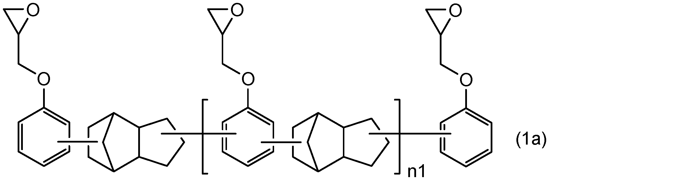
- the epoxy resin represented by the general formula (1) may be an epoxy resin represented by the following general formula (1a).
- n1 has the same meaning as above.
- Examples of commercially available epoxy resin represented by the general formula (1a) include HP-7200L, HP-7200H, HP-7200 (all manufactured by DIC Corporation), XD-1000 (manufactured by Nippon Kayaku Co., Ltd.). Etc.
- R 2 represents a divalent hydrocarbon group.
- the divalent hydrocarbon group for R 2 is, for example, an alkylene group such as a methylene group, an ethylene group, a propylene group, a butylene group or a pentylene group, an arylene group such as a phenylene group or a naphthylene group, or a heteroarylene group such as a pyridylene group.
- You can R 2 is preferably an alkylene group having 1 to 5 carbon atoms.
- Examples of the divalent hydrocarbon group for R 3 , R 4 and R 5 include the same groups as those exemplified for the divalent hydrocarbon group for R 2 .
- R 6 represents a hydrogen atom or a monovalent hydrocarbon group
- n2 represents an integer of 1 to 10.
- Examples of the monovalent hydrocarbon group for R 6 include the same groups as those exemplified for the monovalent hydrocarbon group for R 1 .
- Examples of commercially available epoxy resin represented by the general formula (4) include EHPE3150 (manufactured by Daicel Corporation) and the like.
- the component (A-1) is preferably an epoxy resin represented by the general formula (1), more preferably an epoxy resin represented by the general formula (1a).
- the content of the component (A-1) may be 15 to 100% by mass based on the total amount of the component (A).
- the content of the component (A-1) may be 40% by mass or more, 50% by mass or more, or 60% by mass or more.
- the content of the component (A-1) may be 5% by mass or more, 10% by mass or more, or 20% by mass or more based on the total amount of the adhesive composition.
- the content of the component (A-1) is 5% by mass or more based on the total amount of the adhesive composition, it has better embeddability during thermocompression bonding and also has a high bleeding property during high-temperature pressure treatment. It tends to be suppressed.
- the component (A) may further include (A-2) an aromatic epoxy resin having no alicyclic ring.
- the aromatic epoxy resin having no alicyclic ring is a compound having an aromatic ring and an epoxy group in the molecule and having no alicyclic ring.
- the component (A-2) include bisphenol A type epoxy resin, bisphenol F type epoxy resin, bisphenol S type epoxy resin, phenol novolac type epoxy resin, cresol novolac type epoxy resin, bisphenol A novolac type epoxy resin, and bisphenol F.
- Novolac type epoxy resin stilbene type epoxy resin, triazine skeleton containing epoxy resin, fluorene skeleton containing epoxy resin, triphenolphenol methane type epoxy resin, biphenyl type epoxy resin, xylylene type epoxy resin, phenylaralkyl type epoxy resin, biphenylaralkyl type epoxy resin
- examples thereof include resins, naphthalene type epoxy resins, polyfunctional phenols, diglycidyl ether compounds of polycyclic aromatic compounds such as anthracene, and the like. These may be used alone or in combination of two or more.
- the component (A-2) may be a liquid at 25°C.
- the epoxy equivalent of the component (A-2) is not particularly limited, but may be 90 to 600 g/eq, 100 to 500 g/eq, or 120 to 450 g/eq. When the epoxy equivalent of the component (A-2) is in such a range, better reactivity and fluidity tend to be obtained.
- the content of the component (A-2) may be 0 to 85 mass% based on the total amount of the component (A).
- the content of the component (A-2) may be 60% by mass or less, 50% by mass or less, or 40% by mass or less.
- the component (B) is not particularly limited, and those generally used as a curing agent for thermosetting resins can be used.
- the thermosetting resin contains an epoxy resin
- examples of the component (B) include a phenol resin, an ester compound, an aromatic amine, an aliphatic amine, an acid anhydride and the like. These may be used alone or in combination of two or more.
- the component (B) may contain a phenol resin from the viewpoint of reactivity and stability over time.
- the phenol resin can be used without particular limitation as long as it has a phenolic hydroxyl group in the molecule.
- examples of the phenol resin include phenols such as phenol, cresol, resorcin, catechol, bisphenol A, bisphenol F, phenylphenol and aminophenol, and/or naphthols such as ⁇ -naphthol, ⁇ -naphthol and dihydroxynaphthalene, and formaldehyde.
- Novolak-type phenol resin obtained by condensation or co-condensation with the compound having an aldehyde group under an acidic catalyst allylated bisphenol A, allylated bisphenol F, allylated naphthalenediol, phenol novolac, phenols such as phenol, and/or
- a phenol aralkyl resin synthesized from naphthols and dimethoxyparaxylene or bis(methoxymethyl)biphenyl, a naphthol aralkyl resin, a biphenyl aralkyl type phenol resin, a phenyl aralkyl type phenol resin and the like can be mentioned. These may be used alone or in combination of two or more.
- the phenol resin has a water absorption rate of 2% by mass or less and a thermogravimetric analyzer (TGA) in a constant temperature and humidity tank of 85° C. and 85% RH for 48 hours. It is preferable that the heating mass reduction rate (temperature rising rate: 5° C./min, atmosphere: nitrogen) measured at 350° C. of less than 5% by mass.
- TGA thermogravimetric analyzer
- phenolic resins examples include Phenolite KA series, TD series (manufactured by DIC Corporation), Milex XLC series, XL series (manufactured by Mitsui Chemicals, Inc.) and HE series (manufactured by Air Water Corporation). Can be mentioned.
- the hydroxyl equivalent of the phenol resin is not particularly limited, but may be 80 to 400 g/eq, 90 to 350 g/eq, or 100 to 300 g/eq. When the hydroxyl equivalent of the phenol resin is in such a range, better reactivity and fluidity tend to be obtained.
- the ratio of the epoxy equivalent of the epoxy resin to the hydroxyl equivalent of the phenol resin is From the viewpoint of curability, 0.30/0.70 to 0.70/0.30, 0.35/0.65 to 0.65/0.35, 0.40/0.60 to 0.60/ It may be 0.40, or 0.45/0.55 to 0.55/0.45.
- the equivalent ratio is 0.30/0.70 or more, more sufficient curability tends to be obtained.
- the equivalent ratio is 0.70/0.30 or less, it is possible to prevent the viscosity from becoming too high, and it is possible to obtain more sufficient fluidity.
- the total content of the components (A) and (B) may be 30 to 70% by mass based on the total amount of the adhesive composition.
- the total content of the components (A) and (B) may be 33% by mass or more, 36% by mass or more, or 40% by mass or more, and 65% by mass or less, 60% by mass or less, or 55% by mass. It may be less than or equal to %.
- the adhesiveness tends to be improved.
- the total content of the components (A) and (B) is 70% by mass or less based on the total amount of the adhesive composition, it is possible to prevent the viscosity from becoming too low, and at the time of high temperature pressure treatment. Bleed tends to be more suppressed.
- the adhesive composition according to the present embodiment contains (C) an elastomer.
- the adhesive composition according to the present embodiment contains an elastomer having a (C-1) carboxy group as an elastomer.
- the component (C) is preferably one in which the polymer constituting the elastomer has a glass transition temperature (Tg) of 50° C. or lower.
- the component (C-1) is a compound (elastomer) having a carboxy group in the molecule.
- the component (C-1) as an elastomer, it becomes possible to suppress bleeding during high-temperature pressure treatment while having good embedding properties during thermocompression bonding.
- component (C-1) examples include acrylic resin, polyester resin, polyamide resin, polyimide resin, silicone resin, butadiene resin, acrylonitrile resin and modified products thereof.
- the component (C-1) may contain an acrylic resin having a carboxy group from the viewpoint of solubility and fluidity in a solvent.
- the acrylic resin means a polymer containing a structural unit derived from a (meth)acrylic acid ester.
- the acrylic resin is preferably a polymer containing, as a constitutional unit, a constitutional unit derived from a (meth)acrylic acid ester having a crosslinkable functional group such as an epoxy group and an alcoholic or phenolic hydroxyl group in addition to a carboxy group.
- the acrylic resin may be acrylic rubber such as a copolymer of (meth)acrylic acid ester and acrylonitrile.
- the glass transition temperature (Tg) of the acrylic resin may be -50 to 50°C or -30 to 30°C.
- Tg of the acrylic resin is ⁇ 50° C. or higher, the flexibility of the adhesive composition tends to be prevented from becoming too high. As a result, the film adhesive can be easily cut during wafer dicing, and burrs can be prevented from occurring.
- the Tg of the acrylic resin is 50° C. or less, it is possible to prevent the flexibility of the adhesive composition from decreasing. This tends to make it easier to fill voids when the film adhesive is attached to the wafer. In addition, it becomes possible to prevent chipping at the time of dicing due to deterioration of the adhesiveness of the wafer.
- the glass transition temperature (Tg) means a value measured using a DSC (Thermal Differential Scanning Calorimeter) (for example, "Thermo Plus 2" manufactured by Rigaku Corporation).
- the weight average molecular weight (Mw) of the acrylic resin may be 100,000 to 3,000,000 or 500,000 to 2,000,000.
- Mw means a value measured by gel permeation chromatography (GPC) and converted using a calibration curve based on standard polystyrene.
- the acid value of the component (C-1) may be 1 to 60 mgKOH/g, 2 to 40 mgKOH/g, or 3 to 30 mgKOH/g from the viewpoint of curability.
- the acid value is in such a range, bleeding during high temperature pressure treatment tends to be further suppressed.
- Examples of commercially available products of the component (C-1) (acrylic resin) include SG-70L, SG-708-6, WS-023 EK30, SG-280 EK23 (all manufactured by Nagase ChemteX Corporation).
- the component (C) may further include (C-2) an elastomer having no carboxy group.
- the component (C-1) is a compound (elastomer) having no carboxy group in the molecule.
- component (C-2) examples include acrylic resin, polyester resin, polyamide resin, polyimide resin, silicone resin, butadiene resin, acrylonitrile resin and modified products thereof.
- the component (C-2) may contain an acrylic resin having no carboxy group from the viewpoint of solubility and fluidity in a solvent.
- the acrylic resin means a polymer containing a structural unit derived from a (meth)acrylic acid ester.
- the acrylic resin is preferably a polymer containing, as a constituent unit, a constituent unit derived from a (meth)acrylic acid ester having a crosslinkable functional group such as an epoxy group, an alcoholic or phenolic hydroxyl group.
- the acrylic resin may be acrylic rubber such as a copolymer of (meth)acrylic acid ester and acrylonitrile.
- the glass transition temperature (Tg) of the acrylic resin may be the same as the Tg of the (C-1) component acrylic resin.
- the weight average molecular weight (Mw) of the acrylic resin may be the same as the Mw of the acrylic resin as the component (C-1).
- component (C-2) acrylic resin
- examples of commercially available products of component (C-2) include SG-P3 and SG-80H (both manufactured by Nagase Chemtex Co., Ltd.).
- the content of the component (C) may be 20 to 200 parts by mass or 30 to 100 parts by mass based on 100 parts by mass of the total amount of the components (A) and (B).
- the film adhesive has better handleability (for example, bendability).
- Tend to be When the content of the component (C) is 200 parts by mass or less based on 100 parts by mass of the total amount of the components (A) and (B), it is possible to prevent the adhesive composition from having too high flexibility. Tends to be able to. As a result, it becomes easier to cut the film adhesive during wafer dicing, and it becomes even more possible to prevent the occurrence of burrs.
- Mass ratio of content of component (C-1) to content of component (C) may be 0.05 to 1, 0.10 to 1, 0.20 to 1, 0.40 to 1, or 0.60 to 1.
- the adhesive composition according to the present embodiment may further contain (D) an inorganic filler.
- the inorganic filler include aluminum hydroxide, magnesium hydroxide, calcium carbonate, magnesium carbonate, calcium silicate, magnesium silicate, calcium oxide, magnesium oxide, aluminum oxide, aluminum nitride, aluminum borate whiskers, boron nitride, and crystals. Examples thereof include crystalline silica and amorphous silica. These may be used alone or in combination of two or more. From the viewpoint of further improving the thermal conductivity of the obtained film adhesive, the inorganic filler may contain aluminum oxide, aluminum nitride, boron nitride, crystalline silica or amorphous silica.
- the inorganic filler is aluminum hydroxide, magnesium hydroxide, calcium carbonate, magnesium carbonate, calcium silicate, It may include magnesium silicate, calcium oxide, magnesium oxide, aluminum oxide, crystalline silica or amorphous silica.
- the average particle size of the component (D) may be 0.005 to 0.5 ⁇ m or 0.05 to 0.3 ⁇ m from the viewpoint of further improving the adhesiveness.
- the average particle diameter means a value obtained by converting from the BET specific surface area.
- the component (D) may be surface-treated with a surface-treating agent from the viewpoint of compatibility between the surface and the solvent, other components, etc., and adhesive strength.
- a surface treatment agent include silane coupling agents and the like.
- the functional group of the silane coupling agent include a vinyl group, a (meth)acryloyl group, an epoxy group, a mercapto group, an amino group, a diamino group, an alkoxy group and an ethoxy group.
- the content of the component (D) may be 10 to 90 parts by mass or 10 to 50 parts by mass based on 100 parts by mass of the total amount of the components (A), (B) and (C).
- the content of the component (D) is 10 parts by mass or more based on 100 parts by mass of the total amount of the components (A), (B), and (C)
- the dicing property of the adhesive layer before curing is high.
- the adhesive strength of the adhesive layer after curing tends to be improved.
- the content of the component (D) is 90 parts by mass or less based on 100 parts by mass of the total amount of the components (A), (B), and (C)
- deterioration of fluidity can be suppressed and curing It becomes possible to prevent the elastic modulus of the film adhesive afterwards from becoming too high.
- the adhesive composition according to the present embodiment may contain (E) a curing accelerator.
- the curing accelerator is not particularly limited, and those generally used can be used.
- Examples of the component (E) include imidazoles and their derivatives, organic phosphorus compounds, secondary amines, tertiary amines, and quaternary ammonium salts. These may be used alone or in combination of two or more.
- the component (E) may be an imidazole or a derivative thereof from the viewpoint of reactivity.
- imidazoles examples include 2-methylimidazole, 1-benzyl-2-methylimidazole, 1-cyanoethyl-2-phenylimidazole, 1-cyanoethyl-2-methylimidazole and the like. These may be used alone or in combination of two or more.
- the content of the component (E) is 0.04 to 3 parts by mass or 0.04 to 0.2 part by mass based on 100 parts by mass of the total amount of the components (A), (B), and (C). May be When the content of the component (E) is in such a range, curability and reliability tend to be compatible with each other.
- the adhesive composition according to the present embodiment may further contain an antioxidant, a silane coupling agent, a rheology control agent and the like as other components.
- the content of these components may be 0.02 to 3 parts by mass based on 100 parts by mass of the total amount of the components (A), (B) and (C).
- the adhesive composition according to the present embodiment may be used as an adhesive varnish diluted with a solvent.
- the solvent is not particularly limited as long as it can dissolve components other than the component (D).
- the solvent include aromatic hydrocarbons such as toluene, xylene, mesitylene, cumene and p-cymene; aliphatic hydrocarbons such as hexane and heptane; cyclic alkanes such as methylcyclohexane; tetrahydrofuran, 1,4-dioxane and the like.
- Cyclic ethers such as acetone, methyl ethyl ketone, methyl isobutyl ketone, cyclohexanone, 4-hydroxy-4-methyl-2-pentanone; esters such as methyl acetate, ethyl acetate, butyl acetate, methyl lactate, ethyl lactate, ⁇ -butyrolactone; Carbonic acid esters such as ethylene carbonate and propylene carbonate; amides such as N,N-dimethylformamide, N,N-dimethylacetamide and N-methyl-2-pyrrolidone. These may be used alone or in combination of two or more.
- the solvent may be toluene, xylene, methyl ethyl ketone, methyl isobutyl ketone, or cyclohexane from the viewpoint of solubility and boiling point.
- the solid component concentration in the adhesive varnish may be 10 to 80% by mass, based on the total mass of the adhesive varnish.
- the adhesive varnish should be prepared by mixing and kneading the components (A), (B), (C), and solvent, and, if necessary, the components (D), (E), and other components. Can be prepared by.
- the mixing and kneading can be carried out by appropriately combining an ordinary stirrer, a raker, a three-roller, a ball mill, a bead mill and other dispersing machines.
- the mixing time can be shortened by previously mixing the component (D) and the low molecular weight component and then blending the high molecular weight component.
- air bubbles in the varnish may be removed by vacuum deaeration or the like.
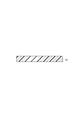
- FIG. 1 is a schematic cross-sectional view showing a film adhesive according to one embodiment.
- the film adhesive 10 is formed by forming the above adhesive composition into a film.
- the film adhesive 10 may be in a semi-cured (B stage) state.
- Such a film adhesive 10 can be formed by applying an adhesive composition to a support film.
- the adhesive varnish 10 can be formed by applying the adhesive varnish to the support film and heating and drying the solvent to remove the solvent.
- the supporting film is not particularly limited, and examples thereof include films of polytetrafluoroethylene, polyethylene, polypropylene, polymethylpentene, polyethylene terephthalate, polyimide and the like.
- the thickness of the support film may be, for example, 60 to 200 ⁇ m or 70 to 170 ⁇ m.
- a known method can be used, and examples thereof include a knife coating method, a roll coating method, a spray coating method, a gravure coating method, a bar coating method, and a curtain coating method.
- the heating and drying conditions are not particularly limited as long as the solvent used is sufficiently volatilized, but may be, for example, 50 to 200° C. and 0.1 to 90 minutes.
- the thickness of the film adhesive can be adjusted appropriately according to the application.
- the thickness of the film adhesive may be 20 to 200 ⁇ m, 30 to 200 ⁇ m, or 40 to 150 ⁇ m from the viewpoint of sufficiently embedding the irregularities of the semiconductor chip, the wires, the wiring circuit of the substrate and the like.
- FIG. 2 is a schematic cross-sectional view showing the adhesive sheet according to the embodiment.
- the adhesive sheet 100 includes a base material 20 and the above film adhesive 10 provided on the base material.
- the base material 20 is not particularly limited, but may be a base material film.
- the base film may be similar to the support film described above.
- the base material 20 may be a dicing tape.
- Such an adhesive sheet can be used as a dicing die bonding integrated type adhesive sheet. In this case, since the process of laminating on the semiconductor wafer is performed once, the work efficiency can be improved.
- the dicing tape examples include plastic films such as polytetrafluoroethylene film, polyethylene terephthalate film, polyethylene film, polypropylene film, polymethylpentene film and polyimide film. Further, the dicing tape may be subjected to surface treatment such as primer coating, UV treatment, corona discharge treatment, polishing treatment and etching treatment, if necessary.
- the dicing tape is preferably adhesive.
- Such a dicing tape may be one in which the above-mentioned plastic film is provided with tackiness, or one in which an adhesive layer is provided on one surface of the above-mentioned plastic film.
- the adhesive sheet 100 can be formed by applying an adhesive composition to a base film, similarly to the method for forming the film adhesive described above.
- the method of applying the adhesive composition to the substrate 20 may be the same as the method of applying the adhesive composition to the support film.
- the adhesive sheet 100 may be formed by using a film-like adhesive agent prepared in advance.
- the adhesive sheet 100 can be formed by laminating under a predetermined condition (for example, room temperature (20° C.) or a heated state) using a roll laminator, a vacuum laminator, or the like. Since the adhesive sheet 100 can be continuously manufactured and is highly efficient, it is preferably formed by using a roll laminator in a heated state.
- the thickness of the film adhesive 10 may be 20 to 200 ⁇ m, 30 to 200 ⁇ m, or 40 to 150 ⁇ m from the viewpoint of embedding of irregularities such as semiconductor chips, wires, and wiring circuits of the substrate.
- the thickness of the film adhesive 10 is 20 ⁇ m or more, more sufficient adhesive force tends to be obtained, and when the thickness of the film adhesive 10 is 200 ⁇ m or less, it is economical and the semiconductor device is provided. It is possible to meet the demand for downsizing.
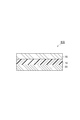
- FIG. 3 is a schematic cross-sectional view showing an adhesive sheet according to another embodiment.
- the adhesive sheet 110 further includes a protective film 30 laminated on the surface of the film adhesive 10 opposite to the base material 20.
- the protective film 30 may be the same as the support film described above.
- the thickness of the protective film may be, for example, 15 to 200 ⁇ m or 70 to 170 ⁇ m.
- FIG. 4 is a schematic cross-sectional view showing a semiconductor device according to one embodiment.
- the first semiconductor element Wa of the first stage is wire-bonded to the substrate 14 via the first wire 88, and the second semiconductor element Waa is formed on the first semiconductor element Wa.
- the semiconductor device is a semiconductor device in which at least a part of the first wire 88 is embedded in the film adhesive 10 by being pressure-bonded with the film adhesive 10.
- the semiconductor device is a semiconductor device in which the first wire 88 and the first semiconductor element Wa are embedded even if it is a wire-embedded type semiconductor device in which at least a part of the first wire 88 is embedded. May be.
- the substrate 14 and the second semiconductor element Waa are further electrically connected via the second wire 98, and the second semiconductor element Waa is sealed by the sealing material 42. ing.
- the thickness of the first semiconductor element Wa may be 10 to 170 ⁇ m, and the thickness of the second semiconductor element Waa may be 20 to 400 ⁇ m.
- the first semiconductor element Wa embedded in the film adhesive 10 is a controller chip for driving the semiconductor device 200.
- the substrate 14 is composed of an organic substrate 90 having two circuit patterns 84 and 94 formed on the surface.
- the first semiconductor element Wa is pressure-bonded onto the circuit pattern 94 via the adhesive 41.
- the second semiconductor element Waa is sandwiched by the film adhesive 10 so that the circuit pattern 94 to which the first semiconductor element Wa is not pressure-bonded, the first semiconductor element Wa, and a part of the circuit pattern 84 are covered. It is pressure bonded to the substrate 14.
- the film-like adhesive 10 is embedded in the steps of the unevenness caused by the circuit patterns 84 and 94 on the substrate 14. Then, the second semiconductor element Waa, the circuit pattern 84, and the second wire 98 are sealed by the resin sealing material 42.
- a method of manufacturing a semiconductor device includes a first wire bonding step of electrically connecting a first semiconductor element on a substrate via a first wire, and a second semiconductor element on one side, At least a part of the first wire is formed into a film by press-bonding the laminating step of attaching the above film adhesive and the second semiconductor element to which the film adhesive is attached via the film adhesive. Bonding step of embedding in a linear adhesive.
- the semiconductor device 200 is a semiconductor device in which the first wire 88 and the first semiconductor element Wa are embedded, and is manufactured by the following procedure.
- the first semiconductor element Wa having the adhesive 41 is pressure-bonded onto the circuit pattern 94 on the substrate 14, and the first semiconductor element Wa and the circuit pattern 84 on the substrate 14 are connected via the first wire 88.
- the semiconductor element Wa of No. 1 is electrically connected by bonding (first wire bonding step).
- the adhesive sheet 100 is laminated on one surface of the semiconductor wafer (for example, thickness 100 ⁇ m, size: 8 inches), and the base material 20 is peeled off, whereby the film adhesive 10 (for example, thickness A thickness of 110 ⁇ m). Then, a dicing tape is attached to the film adhesive 10, and then the film is diced into a predetermined size (for example, 7.5 mm square), so that the film adhesive 10 is attached to the second portion as shown in FIG.
- the semiconductor element Waa of is obtained (laminating step).
- the temperature condition of the laminating process may be 50 to 100°C or 60 to 80°C.
- the temperature of the laminating step is 50° C. or higher, good adhesion with the semiconductor wafer can be obtained.
- the temperature of the laminating step is 100° C. or less, the film adhesive 10 is prevented from excessively flowing during the laminating step, so that it is possible to prevent a change in thickness and the like.
- dicing method for example, blade dicing using a rotary blade, a method of cutting the film adhesive with a laser or both the wafer and the film adhesive, and the like can be mentioned.
- the second semiconductor element Waa to which the film adhesive 10 is attached is pressure-bonded to the substrate 14 to which the first semiconductor element Wa is bonded and connected via the first wire 88.
- the second semiconductor element Waa to which the film adhesive 10 is attached is covered with the film adhesive 10 so that the first wire 88 and the first semiconductor element Wa are covered.
- the second semiconductor element Waa is fixed to the substrate 14 by pressure bonding the second semiconductor element Waa to the substrate 14 (die bonding step).
- the film adhesive 10 is pressure-bonded for 0.5 to 3.0 seconds under the conditions of 80 to 180° C. and 0.01 to 0.50 MPa.
- the film adhesive 10 is subjected to a high-temperature pressure treatment under pressure and heating at 60 to 175° C. and 0.3 to 0.7 MPa for 5 minutes or more.
- the circuit pattern 84, the second wire 98 and the second semiconductor element Waa are sealed with the sealing material 42.
- the semiconductor device 200 can be manufactured through such steps.
- the semiconductor device may be a wire-embedded semiconductor device in which at least a part of the first wire 88 is embedded.
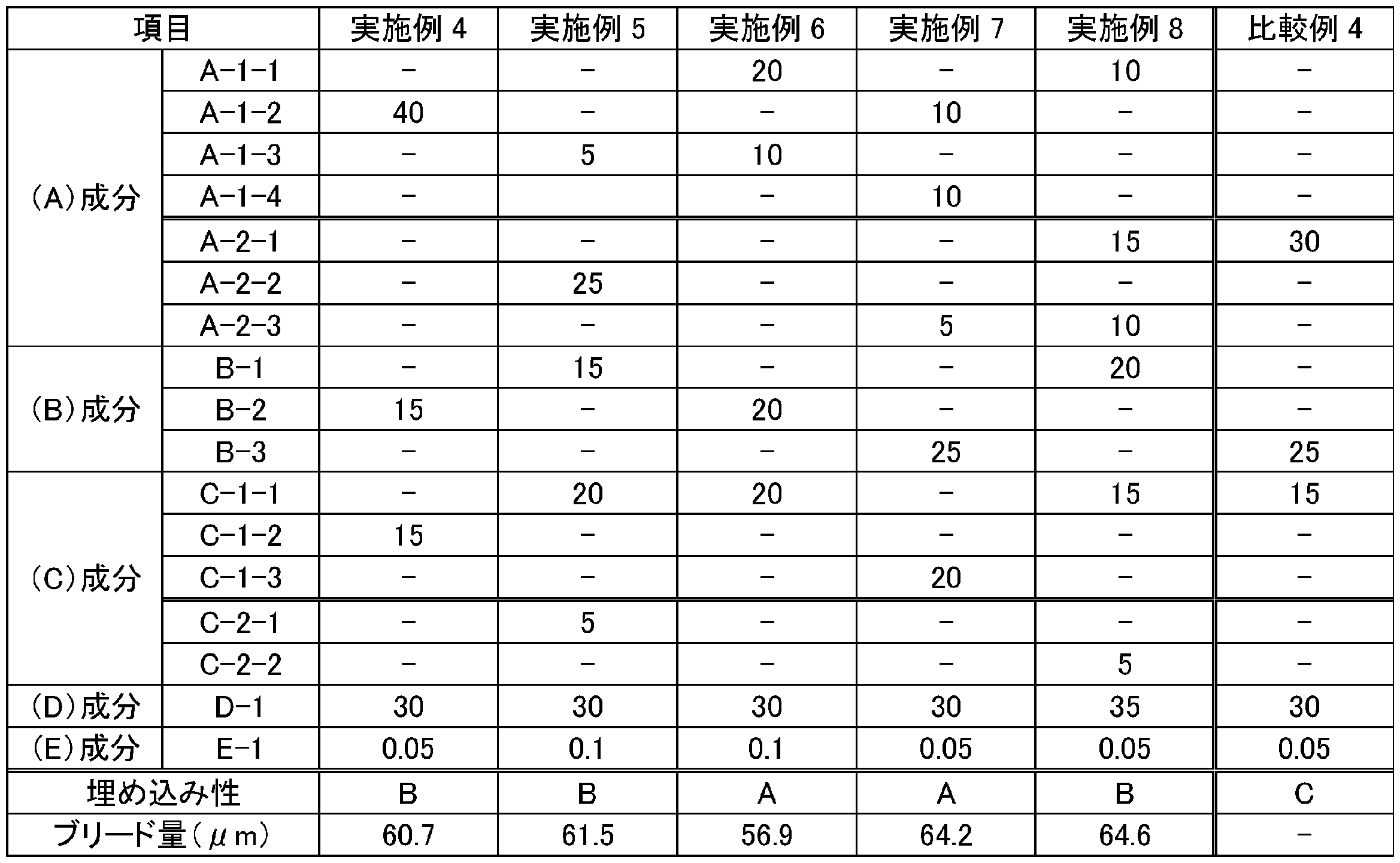
- Table 1 The components in Table 1, Table 2 and Table 3 are as follows.
- Epoxy resin having alicyclic ring A-1-1 Epoxy resin represented by general formula (1a) (epoxy resin having dicyclopentadiene structure), DIC stock Made by the company, product name: HP-7200L, epoxy equivalent: 250-280g/eq
- A-1-2 Epoxy resin represented by general formula (1a) (epoxy resin having dicyclopentadiene structure), manufactured by Nippon Kayaku Co., Ltd., trade name: XD-1000, epoxy equivalent: 254 g/eq.
- A-1-3 Epoxy resin represented by the general formula (2) (liquid at 25° C.), manufactured by Daicel Corporation, trade name: Celoxide 2021P, epoxy equivalent: 128 to 145 g/eq
- A-1-4 Epoxy resin represented by the general formula (4), manufactured by Daicel Corporation, trade name: EHPE3150, epoxy equivalent: 170 to 190 g/eq (A-2)
- A-2-3 Bisphenol F type epoxy resin (liquid at 25° C.), manufactured by DIC Corporation, trade name: EXA-830CRP, epoxy equivalent: 159 g/eq (B) Curing agent B-1
- C-1-3 Acrylic resin containing carboxy group (acrylic rubber), manufactured by Nagase Chemtex Co., Ltd., trade name: WS-023 EK30, weight average molecular weight: 500,000, acid value: 20 mgKOH/g, Tg: -10°C (C-2)
- Elastomer having no carboxy group C-2-1 Epoxy group-containing acrylic resin (acrylic rubber) containing no carboxy group, manufactured by Nagase Chemtex Co., Ltd., trade name: SG-P3 solvent modified product, weight average Molecular weight: 800,000, Tg: 12°C C-2-2: Carboxy group-free epoxy group-containing acrylic resin (acrylic rubber), manufactured by Nagase Chemtex Co., Ltd., trade name: SG-80H, weight average molecular weight: 350,000, Tg: 11° C.
- D Inorganic filler D-1: Silica filler dispersion, fused silica, manufactured by Admatechs Co., Ltd., trade name: SC2050-HLG, average particle size: 0.50 ⁇ m
- E Curing accelerator E-1:1-cyanoethyl-2-phenylimidazole, manufactured by Shikoku Chemicals Co., Ltd., trade name: Cureazole 2PZ-CN
- the embeddability of the adhesive sheet was evaluated by making the following evaluation samples.
- the film adhesive (thickness 110 ⁇ m) obtained above was peeled off the base film and attached to a dicing tape to obtain a dicing die bonding integrated adhesive sheet.
- a semiconductor wafer (8 inches) having a thickness of 100 ⁇ m was heated to 70° C. and attached to the adhesive side.
- the semiconductor chip A was obtained by dicing this semiconductor wafer into 7.5 mm square.
- a dicing die bonding integrated adhesive sheet manufactured by Hitachi Chemical Co., Ltd., trade name: HR9004-10 (thickness 10 ⁇ m) was prepared and heated to 70° C.
- a semiconductor wafer (8 inches) with a thickness of 50 ⁇ m. Pasted Then, this semiconductor wafer was diced into a 4.5 mm square to obtain a semiconductor chip B with a die bonding film.
- a 260 ⁇ m-thick evaluation substrate coated with a solder resist (manufactured by Taiyo Nissan Corporation, product name: AUS308) is prepared, and a solder for the die bonding film of the semiconductor chip B with the die bonding film and the evaluation substrate is prepared. It was pressure-bonded under the conditions of 120° C., 0.20 MPa, and 2 seconds so that it was in contact with the resist.
- the film-like adhesive of the semiconductor chip A and the semiconductor wafer of the semiconductor chip B were pressure-bonded under the conditions of 120° C., 0.20 MPa, and 1.5 seconds to obtain an evaluation sample.
- the alignment was performed so that the semiconductor chip B, which had been previously pressure-bonded, was at the center of the semiconductor chip A.
- the evaluation sample thus obtained was observed with an ultrasonic digital image diagnostic apparatus (Insight Co., Ltd., probe: 75 MHz) for the presence or absence of observation of voids, and when voids were observed, per unit area
- the void area ratio was calculated, and the results of these analyzes were evaluated as embeddability.
- the evaluation criteria are as follows. The results are shown in Table 1, Table 2 and Table 3. A: No void was observed. B: Voids were observed, but the ratio was less than 5 area %. C: Voids were observed, and the ratio was 5 area% or more.
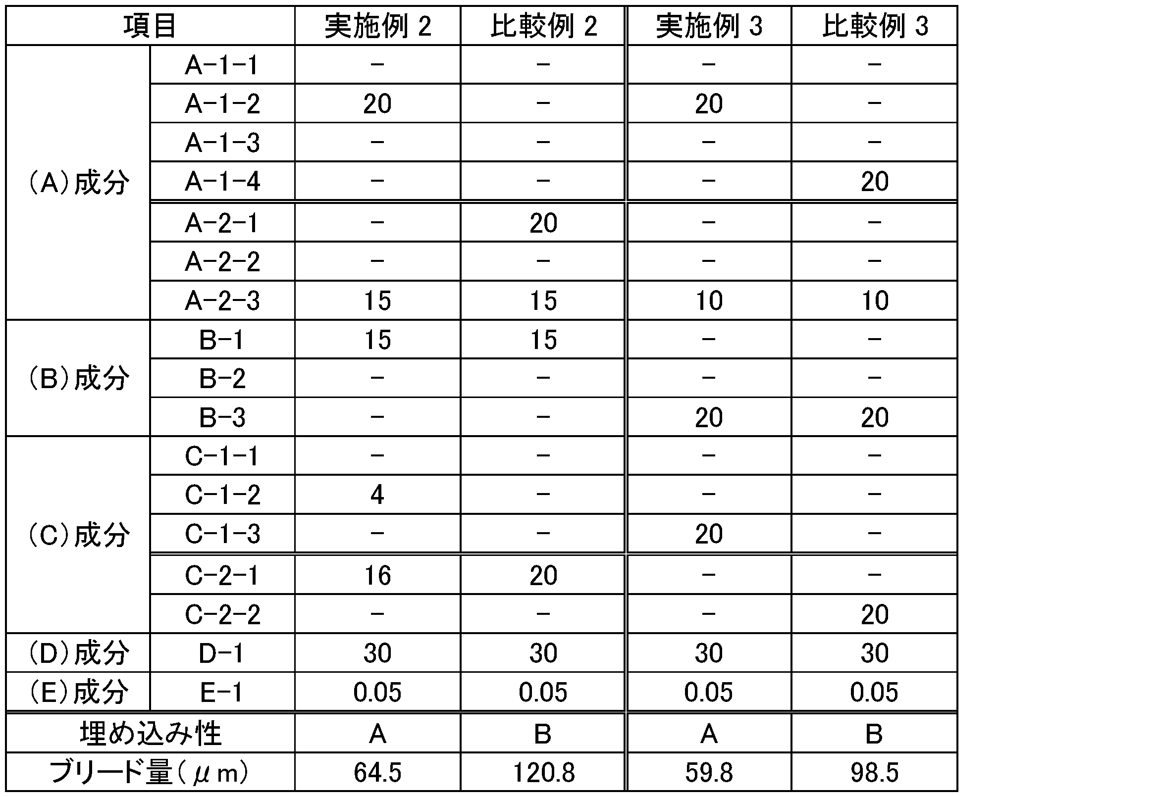
- Example 1 As shown in Table 1, the adhesive composition of Example 1 containing an epoxy resin having an alicyclic ring, and the elastomer containing an elastomer having a carboxy group, was not included in Comparative Examples 1-1 to 1-3. Compared with the adhesive composition of No. 3, it was possible to suppress bleeding during high-temperature pressure treatment while maintaining good embeddability. Also, from Examples 2 and 3 in Table 2 and Examples 4 to 8 in Table 3, even when an epoxy resin having another alicyclic ring is used or when an elastomer having another carboxy group is used, It turns out that there is a similar tendency. From these results, it was confirmed that the adhesive composition according to the present invention has good embeddability during thermocompression bonding and can suppress bleeding during high-temperature pressure treatment.
- the adhesive composition according to the present invention has a good embedding property during thermocompression bonding and can suppress bleeding during high-temperature pressure treatment. Therefore, the adhesive composition is formed into a film.
- the film adhesive can be useful as FOD (Film Over Die) which is a chip-embedded film adhesive or FOW (Film Over Wire) which is a wire-embedded film adhesive.
Landscapes
- Chemical & Material Sciences (AREA)
- Organic Chemistry (AREA)
- Inorganic Chemistry (AREA)
- Adhesives Or Adhesive Processes (AREA)
- Adhesive Tapes (AREA)
- Epoxy Resins (AREA)
- Die Bonding (AREA)
Abstract
Description
本実施形態に係る接着剤組成物は、(A)熱硬化性樹脂と、(B)硬化剤と、(C)エラストマーと、を含有する。接着剤組成物は、熱硬化性であり、半硬化(Bステージ)状態を経て、硬化処理後に完全硬化物(Cステージ)状態となり得る。
熱硬化性樹脂は、接着性の観点から、エポキシ樹脂を含んでいてよい。本実施形態に係る接着剤組成物は、熱硬化性樹脂として、(A-1)脂環式環を有するエポキシ樹脂を含む。




(B)成分は、特に制限なく、熱硬化性樹脂の硬化剤として一般的に使用されているものを用いることができる。熱硬化性樹脂がエポキシ樹脂を含む場合、(B)成分としては、例えば、フェノール樹脂、エステル化合物、芳香族アミン、脂肪族アミン、酸無水物等が挙げられる。これらは、1種を単独で又は2種以上を組み合わせて用いてもよい。これらの中でも、反応性及び経時安定性の観点から、(B)成分はフェノール樹脂を含んでいてよい。
本実施形態に係る接着剤組成物は、(C)エラストマーを含有する。本実施形態に係る接着剤組成物は、エラストマーとして、(C-1)カルボキシ基を有するエラストマーを含む。(C)成分は、エラストマーを構成する重合体のガラス転移温度(Tg)が50℃以下であるものが好ましい。
本実施形態に係る接着剤組成物は、(D)無機フィラーをさらに含有していてもよい。無機フィラーとしては、例えば、水酸化アルミニウム、水酸化マグネシウム、炭酸カルシウム、炭酸マグネシウム、ケイ酸カルシウム、ケイ酸マグネシウム、酸化カルシウム、酸化マグネシウム、酸化アルミニウム、窒化アルミニウム、ホウ酸アルミウィスカ、窒化ホウ素、結晶性シリカ、非晶性シリカ等が挙げられる。これらは1種を単独で用いてもよく、2種以上を組み合わせて用いてもよい。得られるフィルム状接着剤の熱伝導性がより向上する観点から、無機フィラーは、酸化アルミニウム、窒化アルミニウム、窒化ホウ素、結晶性シリカ又は非晶性シリカを含んでいてよい。また、接着剤組成物の溶融粘度を調整する観点及び接着剤組成物にチキソトロピック性を付与する観点から、無機フィラーは、水酸化アルミニウム、水酸化マグネシウム、炭酸カルシウム、炭酸マグネシウム、ケイ酸カルシウム、ケイ酸マグネシウム、酸化カルシウム、酸化マグネシウム、酸化アルミニウム、結晶性シリカ又は非晶性シリカを含んでいてよい。
本実施形態に係る接着剤組成物は、(E)硬化促進剤を含有していてよい。硬化促進剤は、特に限定されず、一般に使用されるものを用いることができる。(E)成分としては、例えば、イミダゾール類及びその誘導体、有機リン系化合物、第二級アミン類、第三級アミン類、第四級アンモニウム塩等が挙げられる。これらは、1種を単独で又は2種以上を組み合わせて用いてもよい。これらの中でも、反応性の観点から(E)成分はイミダゾール類及びその誘導体であってよい。
本実施形態に係る接着剤組成物は、その他の成分として、抗酸化剤、シランカップリング剤、レオロジーコントロール剤等をさらに含有していてもよい。これらの成分の含有量は、(A)成分、(B)成分、及び(C)成分の総量100質量部に対して、0.02~3質量部であってよい。
図1は、一実施形態に係るフィルム状接着剤を示す模式断面図である。フィルム状接着剤10は、上述の接着剤組成物をフィルム状に形成してなるものである。フィルム状接着剤10は、半硬化(Bステージ)状態であってよい。このようなフィルム状接着剤10は、接着剤組成物を支持フィルムに塗布することによって形成することができる。接着剤ワニスを用いる場合は、接着剤ワニスを支持フィルムに塗布し、溶剤を加熱乾燥して除去することによってフィルム状接着剤10を形成することができる。
図2は、一実施形態に係る接着シートを示す模式断面図である。接着シート100は、基材20と基材上に設けられた上述のフィルム状接着剤10とを備える。
図4は、一実施形態に係る半導体装置を示す模式断面図である。半導体装置200は、基板14に、第1のワイヤ88を介して1段目の第1の半導体素子Waがワイヤボンディング接続されると共に、第1の半導体素子Wa上に、第2の半導体素子Waaがフィルム状接着剤10を介して圧着されることで、第1のワイヤ88の少なくとも一部がフィルム状接着剤10に埋め込まれてなる半導体装置である。半導体装置は、第1のワイヤ88の少なくとも一部が埋め込まれてなるワイヤ埋め込み型の半導体装置であっても、第1のワイヤ88及び第1の半導体素子Waが埋め込まれてなる半導体装置であってもよい。また、半導体装置200では、基板14と第2の半導体素子Waaとがさらに第2のワイヤ98を介して電気的に接続されると共に、第2の半導体素子Waaが封止材42により封止されている。
本実施形態に係る半導体装置の製造方法は、基板上に第1のワイヤを介して第1の半導体素子を電気的に接続する第1のワイヤボンディング工程と、第2の半導体素子の片面に、上述のフィルム状接着剤を貼付するラミネート工程と、フィルム状接着剤が貼付された第2の半導体素子を、フィルム状接着剤を介して圧着することで、第1のワイヤの少なくとも一部をフィルム状接着剤に埋め込むダイボンド工程と、を備える。
<接着シートの作製>
以下に示す各成分を表1、表2、及び表3に示した配合割合(質量部)で混合し、溶媒としてシクロヘキサノンを用いて固形分40質量%の接着剤組成物のワニスを調製した。次に、得られたワニスを100メッシュのフィルターでろ過し、真空脱泡した。真空脱泡後のワニスを、基材フィルムとして、厚さ38μmの離型処理を施したポリエチレンテレフタレート(PET)フィルム上に塗布した。塗布したワニスを、90℃で5分間、続いて140℃で5分間の2段階で加熱乾燥した。このようにして、基材フィルム上に、半硬化(Bステージ)状態にある厚さ110μmのフィルム状接着剤を備える接着シートを得た。
(A-1)脂環式環を有するエポキシ樹脂
A-1-1:一般式(1a)で表されるエポキシ樹脂(ジシクロペンタジエン構造を有するエポキシ樹脂)、DIC株式会社製、商品名:HP-7200L、エポキシ当量:250~280g/eq
A-1-2:一般式(1a)で表されるエポキシ樹脂(ジシクロペンタジエン構造を有するエポキシ樹脂)、日本化薬株式会社製、商品名:XD-1000、エポキシ当量:254g/eq
A-1―3:一般式(2)で表されるエポキシ樹脂(25℃で液体)、株式会社ダイセル製、商品名:セロキサイド2021P、エポキシ当量:128~145g/eq
A-1-4:一般式(4)で表されるエポキシ樹脂、株式会社ダイセル製、商品名:EHPE3150、エポキシ当量:170~190g/eq
(A-2)脂環式環を有しない芳香族エポキシ樹脂
A-2-1:多官能芳香族エポキシ樹脂、株式会社プリンテック製、商品名:VG3101L、エポキシ当量:210g/eq
A-2-2:クレゾールノボラック型エポキシ樹脂、新日鉄住金化学株式会社製、商品名:YDCN-700-10、エポキシ当量:209g/eq
A-2-3:ビスフェノールF型エポキシ樹脂(25℃で液体)、DIC株式会社製、商品名:EXA-830CRP、エポキシ当量:159g/eq
(B)硬化剤
B-1:ビスフェノールAノボラック型フェノール樹脂、DIC株式会社製、商品名:LF-4871、水酸基当量:118g/eq
B-2:フェニルアラルキル型フェノール樹脂、三井化学株式会社製、商品名:XLC-LL、水酸基当量:175g/eq
B-3:フェニルアラルキル型フェノール樹脂、エア・ウォーター株式会社製、商品名:HE100C-30、水酸基当量:170g/eq
(C)エラストマー
(C-1)カルボキシ基を有するエラストマー
C-1-1:カルボキシ基含有アクリル樹脂(アクリルゴム)、ナガセケムテックス株式会社製、商品名:SG-70L、重量平均分子量:90万、酸価:5mgKOH/g、Tg:-13℃
C-1-2:カルボキシ基含有アクリル樹脂(アクリルゴム)、ナガセケムテックス株式会社製、商品名:SG-708-6、重量平均分子量:70万、酸価:9mgKOH/g、Tg:4℃
C-1-3:カルボキシ基含有アクリル樹脂(アクリルゴム)、ナガセケムテックス株式会社製、商品名:WS-023 EK30、重量平均分子量:50万、酸価:20mgKOH/g、Tg:-10℃
(C-2)カルボキシ基を有しないエラストマー
C-2-1:カルボキシ基非含有エポキシ基含有アクリル樹脂(アクリルゴム)、ナガセケムテックス株式会社製、商品名:SG-P3溶剤変更品、重量平均分子量:80万、Tg:12℃
C-2-2:カルボキシ基非含有エポキシ基含有アクリル樹脂(アクリルゴム)、ナガセケムテックス株式会社製、商品名:SG-80H、重量平均分子量:35万、Tg:11℃
(D)無機フィラー
D-1:シリカフィラー分散液、溶融シリカ、株式会社アドマテックス製、商品名:SC2050-HLG、平均粒径:0.50μm
(E)硬化促進剤
E-1:1-シアノエチル-2-フェニルイミダゾール、四国化成工業株式会社製、商品名:キュアゾール2PZ-CN
得られた接着シートについて、埋め込み性及びブリード量の評価を行った。
接着シートの埋め込み性を以下の評価サンプルを作製して評価した。上記で得られたフィルム状接着剤(厚さ110μm)を、基材フィルムを剥がし、ダイシングテープに貼り付け、ダイシングダイボンディング一体型接着シートを得た。次に、厚さ100μmの半導体ウェハ(8インチ)を、接着剤側に70℃に加熱して貼り付けた。その後、この半導体ウェハを7.5mm角にダイシングすることによって、半導体チップAを得た。次に、ダイシングダイボンディング一体型接着シート(日立化成株式会社製、商品名:HR9004-10)(厚さ10μm)を用意し、厚さ50μmの半導体ウェハ(8インチ)に70℃に加熱して貼り付けた。その後、この半導体ウェハを4.5mm角にダイシングすることによって、ダイボンディングフィルム付きの半導体チップBを得た。次いで、ソルダーレジスト(太陽日酸株式会社製、商品名:AUS308)を塗布した総厚さ260μmの評価用基板を用意し、ダイボンディングフィルム付きの半導体チップBのダイボンディングフィルムと評価用基板のソルダーレジストとが接するように、120℃、0.20MPa、2秒間の条件で圧着した。その後、半導体チップAのフィルム状接着剤と半導体チップBの半導体ウェハとが接するように、120℃、0.20MPa、1.5秒間の条件で圧着し、評価サンプルを得た。この際、先に圧着している半導体チップBが半導体チップAの中央となるように位置合わせを行った。このようにして得られた評価サンプルを超音波デジタル画像診断装置(インサイト株式会社製、プローブ:75MHz)にてボイドの観測の有無を観測し、ボイドが観測された場合は、単位面積あたりのボイドの面積の割合を算出し、これらの分析結果を埋め込み性として評価した。評価基準は、以下のとおりである。結果を表1、表2、及び表3に示す。
A:ボイドが観測されなかった。
B:ボイドが観測されたが、その割合が5面積%未満であった。
C:ボイドが観測され、その割合が5面積%以上であった。
上記埋め込み性評価で「A」又は「B」であったものについて、ブリード量評価を行った。上記埋め込み性評価で作製した評価サンプルと同様にして、サンプルを作製し、加圧オーブンを用いて、140℃、0.7MPa、30分の条件で高温加圧処理(加圧キュア)を行い、ブリード評価用サンプルとした。顕微鏡を用いて、評価サンプルの4辺の中心から、フィルム状接着剤のはみ出し量を測長し、その最大値をブリード量とした。結果を表1、表2、及び表3に示す。

Claims (13)
- 熱硬化性樹脂と、硬化剤と、エラストマーと、を含有し、
前記熱硬化性樹脂が脂環式環を有するエポキシ樹脂を含み、
前記エラストマーがカルボキシ基を有するエラストマーを含む、接着剤組成物。 - 前記硬化剤がフェノール樹脂を含む、請求項1に記載の接着剤組成物。
- 前記エラストマーがアクリル樹脂を含む、請求項1又は2に記載の接着剤組成物。
- 前記エラストマーがカルボキシ基を有しないエラストマーをさらに含む、請求項1~3のいずれか一項に記載の接着剤組成物。
- 前記熱硬化性樹脂が脂環式環を有しない芳香族エポキシ樹脂をさらに含む、請求項1~4のいずれか一項に記載の接着剤組成物。
- 前記脂環式環を有しない芳香族エポキシ樹脂が25℃で液体である、請求項5に記載の接着剤組成物。
- 無機フィラーをさらに含有する、請求項1~6のいずれか一項に記載の接着剤組成物。
- 硬化促進剤をさらに含有する、請求項1~7のいずれか一項に記載の接着剤組成物。
- 請求項1~8のいずれか一項に記載の接着剤組成物をフィルム状に形成してなる、フィルム状接着剤。
- 基材と、
前記基材上に設けられた、請求項9に記載のフィルム状接着剤と、
を備える、接着シート。 - 前記基材がダイシングテープである、請求項10に記載の接着シート。
- 前記フィルム状接着剤の前記基材とは反対側の面に積層された保護フィルムをさらに備える、請求項10又は11に記載の接着シート。
- 基板上に第1のワイヤを介して第1の半導体素子を電気的に接続するワイヤボンディング工程と、
第2の半導体素子の片面に、請求項9に記載のフィルム状接着剤を貼付するラミネート工程と、
前記フィルム状接着剤が貼付された第2の半導体素子を、前記フィルム状接着剤を介して圧着することで、前記第1のワイヤの少なくとも一部を前記フィルム状接着剤に埋め込むダイボンド工程と、
を備える、半導体装置の製造方法。
Priority Applications (6)
| Application Number | Priority Date | Filing Date | Title |
|---|---|---|---|
| SG11202107968VA SG11202107968VA (en) | 2019-01-28 | 2019-01-28 | Adhesive composition, film-like adhesive, adhesive sheet and method for producing semiconductor device |
| JP2020568895A JP7327416B2 (ja) | 2019-01-28 | 2019-01-28 | 接着剤組成物、フィルム状接着剤、接着シート、及び半導体装置の製造方法 |
| CN201980090381.8A CN113348221B (zh) | 2019-01-28 | 2019-01-28 | 胶黏剂组合物、膜状胶黏剂、胶黏剂片及半导体装置的制造方法 |
| KR1020217024415A KR102710946B1 (ko) | 2019-01-28 | 2019-01-28 | 접착제 조성물, 필름상 접착제, 접착 시트, 및 반도체 장치의 제조 방법 |
| PCT/JP2019/002789 WO2020157805A1 (ja) | 2019-01-28 | 2019-01-28 | 接着剤組成物、フィルム状接着剤、接着シート、及び半導体装置の製造方法 |
| TW109102154A TWI858004B (zh) | 2019-01-28 | 2020-01-21 | 接著劑組成物、膜狀接著劑、接著片及半導體裝置的製造方法 |
Applications Claiming Priority (1)
| Application Number | Priority Date | Filing Date | Title |
|---|---|---|---|
| PCT/JP2019/002789 WO2020157805A1 (ja) | 2019-01-28 | 2019-01-28 | 接着剤組成物、フィルム状接着剤、接着シート、及び半導体装置の製造方法 |
Publications (1)
| Publication Number | Publication Date |
|---|---|
| WO2020157805A1 true WO2020157805A1 (ja) | 2020-08-06 |
Family
ID=71840974
Family Applications (1)
| Application Number | Title | Priority Date | Filing Date |
|---|---|---|---|
| PCT/JP2019/002789 Ceased WO2020157805A1 (ja) | 2019-01-28 | 2019-01-28 | 接着剤組成物、フィルム状接着剤、接着シート、及び半導体装置の製造方法 |
Country Status (6)
| Country | Link |
|---|---|
| JP (1) | JP7327416B2 (ja) |
| KR (1) | KR102710946B1 (ja) |
| CN (1) | CN113348221B (ja) |
| SG (1) | SG11202107968VA (ja) |
| TW (1) | TWI858004B (ja) |
| WO (1) | WO2020157805A1 (ja) |
Cited By (6)
| Publication number | Priority date | Publication date | Assignee | Title |
|---|---|---|---|---|
| WO2022163465A1 (ja) * | 2021-01-28 | 2022-08-04 | 昭和電工マテリアルズ株式会社 | 半導体装置及びその製造方法、並びに、熱硬化性樹脂組成物、接着フィルム及びダイシング・ダイボンディング一体型フィルム |
| JP2022124461A (ja) * | 2021-02-15 | 2022-08-25 | 信越ポリマー株式会社 | 電磁波シールドフィルム、及び電磁波シールドフィルム付きプリント配線板 |
| CN114945268A (zh) * | 2021-02-15 | 2022-08-26 | 信越聚合物株式会社 | 电磁波屏蔽膜和带电磁波屏蔽膜印刷布线板 |
| WO2023182226A1 (ja) * | 2022-03-25 | 2023-09-28 | 株式会社レゾナック | 半導体用接着フィルム、ダイシング・ダイボンディング一体型フィルム、及び半導体装置の製造方法 |
| JP7356534B1 (ja) | 2022-03-30 | 2023-10-04 | 株式会社レゾナック | 半導体用接着フィルム、ダイシングダイボンディングフィルム、及び半導体装置を製造する方法 |
| JP2024008251A (ja) * | 2022-07-07 | 2024-01-19 | リンテック株式会社 | フィルム状接着剤、半導体加工用シート及び半導体装置の製造方法 |
Families Citing this family (1)
| Publication number | Priority date | Publication date | Assignee | Title |
|---|---|---|---|---|
| CN120648416B (zh) * | 2025-08-13 | 2025-12-09 | 武汉市三选科技有限公司 | 一种埋线型黏着薄膜及其制备方法和应用 |
Citations (11)
| Publication number | Priority date | Publication date | Assignee | Title |
|---|---|---|---|---|
| JPH09181128A (ja) * | 1995-12-25 | 1997-07-11 | Bando Chem Ind Ltd | 半導体用接着テープの製造方法 |
| JP2001294843A (ja) * | 2000-04-13 | 2001-10-23 | Toray Ind Inc | 半導体装置用接着剤組成物およびそれを用いた半導体装置用接着剤シートならびに半導体装置 |
| JP2003338580A (ja) * | 2002-05-21 | 2003-11-28 | Toray Ind Inc | 半導体装置用接着剤組成物およびそれを用いた半導体装置用接着剤シート、半導体接続用基板ならびに半導体装置 |
| JP2004059859A (ja) * | 2002-07-31 | 2004-02-26 | Mitsui Chemicals Inc | フィルム状接着剤及びその接着工法並びに該フィルム状接着剤を用いた半導体装置 |
| JP2005126658A (ja) * | 2003-01-07 | 2005-05-19 | Sekisui Chem Co Ltd | 硬化性樹脂組成物、接着性エポキシ樹脂ペースト、接着性エポキシ樹脂シート、導電接続ペースト、導電接続シート及び電子部品接合体 |
| JP2009007424A (ja) * | 2007-06-27 | 2009-01-15 | Shin Etsu Chem Co Ltd | 接着剤組成物、並びにそれを用いた接着シート及びカバーレイフィルム |
| JP2010118636A (ja) * | 2008-10-16 | 2010-05-27 | Sumitomo Bakelite Co Ltd | 半導体装置の製造方法及び半導体装置 |
| JP2011088966A (ja) * | 2009-10-20 | 2011-05-06 | Shin-Etsu Chemical Co Ltd | 接着剤組成物、接着用シート及びダイシング・ダイアタッチフィルム |
| WO2015151960A1 (ja) * | 2014-03-31 | 2015-10-08 | 荒川化学工業株式会社 | プリント配線板用接着剤組成物、積層板およびフレキシブルプリント配線板 |
| JP2016100532A (ja) * | 2014-11-25 | 2016-05-30 | 日東電工株式会社 | 接着シート、ダイシングシート付き接着シート及び半導体装置の製造方法 |
| WO2017195902A1 (ja) * | 2016-05-13 | 2017-11-16 | 日立化成株式会社 | 樹脂組成物、プリプレグ、樹脂付き金属箔、積層板、プリント配線板及び樹脂組成物の製造方法 |
Family Cites Families (9)
| Publication number | Priority date | Publication date | Assignee | Title |
|---|---|---|---|---|
| JP2787842B2 (ja) * | 1992-09-03 | 1998-08-20 | 住友ベークライト株式会社 | 半導体用導電性樹脂ペースト |
| JP2002064111A (ja) * | 2000-08-21 | 2002-02-28 | Sumitomo Bakelite Co Ltd | 半導体用樹脂ペースト及びそれを用いた半導体装置 |
| JP4668001B2 (ja) | 2005-08-18 | 2011-04-13 | リンテック株式会社 | ダイシング・ダイボンド兼用シートおよびこれを用いた半導体装置の製造方法 |
| JP6135202B2 (ja) * | 2013-03-08 | 2017-05-31 | 日立化成株式会社 | 半導体装置及び半導体装置の製造方法 |
| SG10201907601SA (en) * | 2015-03-04 | 2019-10-30 | Lintec Corp | Film-like adhesive composite sheet and method for manufacturing semiconductor device |
| CN109415609B (zh) * | 2016-06-23 | 2021-03-16 | 株式会社寺冈制作所 | 粘接剂组合物及粘接片 |
| KR20190120239A (ko) * | 2017-03-02 | 2019-10-23 | 도아고세이가부시키가이샤 | 플라스틱제 필름 또는 시트용 활성 에너지선 경화형 접착제 조성물 |
| WO2019013336A1 (ja) * | 2017-07-14 | 2019-01-17 | 日立化成株式会社 | 導電性接着剤組成物及びこれを用いた接続構造体 |
| JP7176536B2 (ja) * | 2018-01-30 | 2022-11-22 | 昭和電工マテリアルズ株式会社 | 接着剤組成物、フィルム状接着剤、接着シート、及び半導体装置の製造方法 |
-
2019
- 2019-01-28 JP JP2020568895A patent/JP7327416B2/ja active Active
- 2019-01-28 WO PCT/JP2019/002789 patent/WO2020157805A1/ja not_active Ceased
- 2019-01-28 KR KR1020217024415A patent/KR102710946B1/ko active Active
- 2019-01-28 SG SG11202107968VA patent/SG11202107968VA/en unknown
- 2019-01-28 CN CN201980090381.8A patent/CN113348221B/zh active Active
-
2020
- 2020-01-21 TW TW109102154A patent/TWI858004B/zh active
Patent Citations (11)
| Publication number | Priority date | Publication date | Assignee | Title |
|---|---|---|---|---|
| JPH09181128A (ja) * | 1995-12-25 | 1997-07-11 | Bando Chem Ind Ltd | 半導体用接着テープの製造方法 |
| JP2001294843A (ja) * | 2000-04-13 | 2001-10-23 | Toray Ind Inc | 半導体装置用接着剤組成物およびそれを用いた半導体装置用接着剤シートならびに半導体装置 |
| JP2003338580A (ja) * | 2002-05-21 | 2003-11-28 | Toray Ind Inc | 半導体装置用接着剤組成物およびそれを用いた半導体装置用接着剤シート、半導体接続用基板ならびに半導体装置 |
| JP2004059859A (ja) * | 2002-07-31 | 2004-02-26 | Mitsui Chemicals Inc | フィルム状接着剤及びその接着工法並びに該フィルム状接着剤を用いた半導体装置 |
| JP2005126658A (ja) * | 2003-01-07 | 2005-05-19 | Sekisui Chem Co Ltd | 硬化性樹脂組成物、接着性エポキシ樹脂ペースト、接着性エポキシ樹脂シート、導電接続ペースト、導電接続シート及び電子部品接合体 |
| JP2009007424A (ja) * | 2007-06-27 | 2009-01-15 | Shin Etsu Chem Co Ltd | 接着剤組成物、並びにそれを用いた接着シート及びカバーレイフィルム |
| JP2010118636A (ja) * | 2008-10-16 | 2010-05-27 | Sumitomo Bakelite Co Ltd | 半導体装置の製造方法及び半導体装置 |
| JP2011088966A (ja) * | 2009-10-20 | 2011-05-06 | Shin-Etsu Chemical Co Ltd | 接着剤組成物、接着用シート及びダイシング・ダイアタッチフィルム |
| WO2015151960A1 (ja) * | 2014-03-31 | 2015-10-08 | 荒川化学工業株式会社 | プリント配線板用接着剤組成物、積層板およびフレキシブルプリント配線板 |
| JP2016100532A (ja) * | 2014-11-25 | 2016-05-30 | 日東電工株式会社 | 接着シート、ダイシングシート付き接着シート及び半導体装置の製造方法 |
| WO2017195902A1 (ja) * | 2016-05-13 | 2017-11-16 | 日立化成株式会社 | 樹脂組成物、プリプレグ、樹脂付き金属箔、積層板、プリント配線板及び樹脂組成物の製造方法 |
Cited By (10)
| Publication number | Priority date | Publication date | Assignee | Title |
|---|---|---|---|---|
| WO2022163465A1 (ja) * | 2021-01-28 | 2022-08-04 | 昭和電工マテリアルズ株式会社 | 半導体装置及びその製造方法、並びに、熱硬化性樹脂組成物、接着フィルム及びダイシング・ダイボンディング一体型フィルム |
| JP2022115581A (ja) * | 2021-01-28 | 2022-08-09 | 昭和電工マテリアルズ株式会社 | 半導体装置及びその製造方法、並びに、熱硬化性樹脂組成物、接着フィルム及びダイシング・ダイボンディング一体型フィルム |
| JP2022124461A (ja) * | 2021-02-15 | 2022-08-25 | 信越ポリマー株式会社 | 電磁波シールドフィルム、及び電磁波シールドフィルム付きプリント配線板 |
| CN114945268A (zh) * | 2021-02-15 | 2022-08-26 | 信越聚合物株式会社 | 电磁波屏蔽膜和带电磁波屏蔽膜印刷布线板 |
| JP7654579B2 (ja) | 2021-02-15 | 2025-04-01 | 信越ポリマー株式会社 | 電磁波シールドフィルム、及び電磁波シールドフィルム付きプリント配線板 |
| WO2023182226A1 (ja) * | 2022-03-25 | 2023-09-28 | 株式会社レゾナック | 半導体用接着フィルム、ダイシング・ダイボンディング一体型フィルム、及び半導体装置の製造方法 |
| JP7356534B1 (ja) | 2022-03-30 | 2023-10-04 | 株式会社レゾナック | 半導体用接着フィルム、ダイシングダイボンディングフィルム、及び半導体装置を製造する方法 |
| WO2023190240A1 (ja) * | 2022-03-30 | 2023-10-05 | 株式会社レゾナック | 半導体用接着フィルム、ダイシングダイボンディングフィルム、及び半導体装置を製造する方法 |
| JP2023148409A (ja) * | 2022-03-30 | 2023-10-13 | 株式会社レゾナック | 半導体用接着フィルム、ダイシングダイボンディングフィルム、及び半導体装置を製造する方法 |
| JP2024008251A (ja) * | 2022-07-07 | 2024-01-19 | リンテック株式会社 | フィルム状接着剤、半導体加工用シート及び半導体装置の製造方法 |
Also Published As
| Publication number | Publication date |
|---|---|
| TWI858004B (zh) | 2024-10-11 |
| SG11202107968VA (en) | 2021-08-30 |
| JP7327416B2 (ja) | 2023-08-16 |
| CN113348221B (zh) | 2024-01-09 |
| CN113348221A (zh) | 2021-09-03 |
| TW202035631A (zh) | 2020-10-01 |
| JPWO2020157805A1 (ja) | 2021-11-25 |
| KR20210114009A (ko) | 2021-09-17 |
| KR102710946B1 (ko) | 2024-09-27 |
Similar Documents
| Publication | Publication Date | Title |
|---|---|---|
| JP7327416B2 (ja) | 接着剤組成物、フィルム状接着剤、接着シート、及び半導体装置の製造方法 | |
| JP7472954B2 (ja) | 接着剤組成物、フィルム状接着剤、接着シート、及び半導体装置の製造方法 | |
| JP2026034733A (ja) | 接着剤組成物、フィルム状接着剤、接着シート、及び半導体装置の製造方法 | |
| KR20230129992A (ko) | 필름상 접착제, 다이싱·다이본딩 일체형 필름, 및 반도체장치 및 그 제조 방법 | |
| WO2025084363A1 (ja) | フィルム状接着剤、ダイシング・ダイボンディング一体型フィルム、並びに半導体装置及びその製造方法 | |
| WO2024190884A1 (ja) | フィルム状接着剤、ダイシング・ダイボンディング一体型フィルム、並びに半導体装置及びその製造方法 | |
| WO2024190881A1 (ja) | フィルム状接着剤、ダイシング・ダイボンディング一体型フィルム、並びに半導体装置及びその製造方法 | |
| KR102561428B1 (ko) | 열경화성 수지 조성물, 필름형 접착제, 접착 시트 및 반도체 장치의 제조 방법 | |
| JPWO2020026757A1 (ja) | 接着剤組成物、フィルム状接着剤、接着シート、及び半導体装置の製造方法 | |
| JPWO2019150445A1 (ja) | フィルム状接着剤及びその製造方法、並びに半導体装置及びその製造方法 | |
| WO2025032779A1 (ja) | フィルム状接着剤、ダイシング・ダイボンディング一体型フィルム、並びに半導体装置及びその製造方法 |
Legal Events
| Date | Code | Title | Description |
|---|---|---|---|
| 121 | Ep: the epo has been informed by wipo that ep was designated in this application |
Ref document number: 19912835 Country of ref document: EP Kind code of ref document: A1 |
|
| ENP | Entry into the national phase |
Ref document number: 2020568895 Country of ref document: JP Kind code of ref document: A |
|
| NENP | Non-entry into the national phase |
Ref country code: DE |
|
| ENP | Entry into the national phase |
Ref document number: 20217024415 Country of ref document: KR Kind code of ref document: A |
|
| 32PN | Ep: public notification in the ep bulletin as address of the adressee cannot be established |
Free format text: NOTING OF LOSS OF RIGHTS PURSUANT TO RULE 112(1) EPC (EPO FORM 1205 DATED 20/10/2021) |
|
| 122 | Ep: pct application non-entry in european phase |
Ref document number: 19912835 Country of ref document: EP Kind code of ref document: A1 |