WO2020148909A1 - 接合体及び表面弾性波デバイス - Google Patents
接合体及び表面弾性波デバイス Download PDFInfo
- Publication number
- WO2020148909A1 WO2020148909A1 PCT/JP2019/001552 JP2019001552W WO2020148909A1 WO 2020148909 A1 WO2020148909 A1 WO 2020148909A1 JP 2019001552 W JP2019001552 W JP 2019001552W WO 2020148909 A1 WO2020148909 A1 WO 2020148909A1
- Authority
- WO
- WIPO (PCT)
- Prior art keywords
- substrate
- spinel
- spinel polycrystalline
- piezoelectric substrate
- polycrystalline substrate
- Prior art date
- Legal status (The legal status is an assumption and is not a legal conclusion. Google has not performed a legal analysis and makes no representation as to the accuracy of the status listed.)
- Ceased
Links
Images


Classifications
-
- C—CHEMISTRY; METALLURGY
- C04—CEMENTS; CONCRETE; ARTIFICIAL STONE; CERAMICS; REFRACTORIES
- C04B—LIME, MAGNESIA; SLAG; CEMENTS; COMPOSITIONS THEREOF, e.g. MORTARS, CONCRETE OR LIKE BUILDING MATERIALS; ARTIFICIAL STONE; CERAMICS; REFRACTORIES; TREATMENT OF NATURAL STONE
- C04B37/00—Joining burned ceramic articles with other burned ceramic articles or other articles by heating
- C04B37/001—Joining burned ceramic articles with other burned ceramic articles or other articles by heating directly with other burned ceramic articles
-
- H—ELECTRICITY
- H03—ELECTRONIC CIRCUITRY
- H03H—IMPEDANCE NETWORKS, e.g. RESONANT CIRCUITS; RESONATORS
- H03H9/00—Networks comprising electromechanical or electro-acoustic elements; Electromechanical resonators
- H03H9/25—Constructional features of resonators using surface acoustic waves
-
- C—CHEMISTRY; METALLURGY
- C04—CEMENTS; CONCRETE; ARTIFICIAL STONE; CERAMICS; REFRACTORIES
- C04B—LIME, MAGNESIA; SLAG; CEMENTS; COMPOSITIONS THEREOF, e.g. MORTARS, CONCRETE OR LIKE BUILDING MATERIALS; ARTIFICIAL STONE; CERAMICS; REFRACTORIES; TREATMENT OF NATURAL STONE
- C04B35/00—Shaped ceramic products characterised by their composition; Ceramics compositions; Processing powders of inorganic compounds preparatory to the manufacturing of ceramic products
- C04B35/01—Shaped ceramic products characterised by their composition; Ceramics compositions; Processing powders of inorganic compounds preparatory to the manufacturing of ceramic products based on oxide ceramics
- C04B35/44—Shaped ceramic products characterised by their composition; Ceramics compositions; Processing powders of inorganic compounds preparatory to the manufacturing of ceramic products based on oxide ceramics based on aluminates
- C04B35/443—Magnesium aluminate spinel
-
- C—CHEMISTRY; METALLURGY
- C04—CEMENTS; CONCRETE; ARTIFICIAL STONE; CERAMICS; REFRACTORIES
- C04B—LIME, MAGNESIA; SLAG; CEMENTS; COMPOSITIONS THEREOF, e.g. MORTARS, CONCRETE OR LIKE BUILDING MATERIALS; ARTIFICIAL STONE; CERAMICS; REFRACTORIES; TREATMENT OF NATURAL STONE
- C04B35/00—Shaped ceramic products characterised by their composition; Ceramics compositions; Processing powders of inorganic compounds preparatory to the manufacturing of ceramic products
- C04B35/622—Forming processes; Processing powders of inorganic compounds preparatory to the manufacturing of ceramic products
- C04B35/64—Burning or sintering processes
- C04B35/645—Pressure sintering
- C04B35/6455—Hot isostatic pressing
-
- H—ELECTRICITY
- H03—ELECTRONIC CIRCUITRY
- H03H—IMPEDANCE NETWORKS, e.g. RESONANT CIRCUITS; RESONATORS
- H03H9/00—Networks comprising electromechanical or electro-acoustic elements; Electromechanical resonators
- H03H9/02—Details
- H03H9/02535—Details of surface acoustic wave devices
- H03H9/02543—Characteristics of substrate, e.g. cutting angles
- H03H9/02559—Characteristics of substrate, e.g. cutting angles of lithium niobate or lithium-tantalate substrates
-
- H—ELECTRICITY
- H03—ELECTRONIC CIRCUITRY
- H03H—IMPEDANCE NETWORKS, e.g. RESONANT CIRCUITS; RESONATORS
- H03H9/00—Networks comprising electromechanical or electro-acoustic elements; Electromechanical resonators
- H03H9/02—Details
- H03H9/02535—Details of surface acoustic wave devices
- H03H9/02543—Characteristics of substrate, e.g. cutting angles
- H03H9/02574—Characteristics of substrate, e.g. cutting angles of combined substrates, multilayered substrates, piezoelectrical layers on not-piezoelectrical substrate
-
- H—ELECTRICITY
- H03—ELECTRONIC CIRCUITRY
- H03H—IMPEDANCE NETWORKS, e.g. RESONANT CIRCUITS; RESONATORS
- H03H9/00—Networks comprising electromechanical or electro-acoustic elements; Electromechanical resonators
- H03H9/02—Details
- H03H9/05—Holders or supports
- H03H9/10—Mounting in enclosures
- H03H9/1064—Mounting in enclosures for surface acoustic wave [SAW] devices
- H03H9/1092—Mounting in enclosures for surface acoustic wave [SAW] devices the enclosure being defined by a cover cap mounted on an element forming part of the surface acoustic wave [SAW] device on the side of the IDT's
-
- H—ELECTRICITY
- H03—ELECTRONIC CIRCUITRY
- H03H—IMPEDANCE NETWORKS, e.g. RESONANT CIRCUITS; RESONATORS
- H03H9/00—Networks comprising electromechanical or electro-acoustic elements; Electromechanical resonators
- H03H9/46—Filters
- H03H9/64—Filters using surface acoustic waves
- H03H9/6406—Filters characterised by a particular frequency characteristic
- H03H9/6413—SAW comb filters
-
- C—CHEMISTRY; METALLURGY
- C04—CEMENTS; CONCRETE; ARTIFICIAL STONE; CERAMICS; REFRACTORIES
- C04B—LIME, MAGNESIA; SLAG; CEMENTS; COMPOSITIONS THEREOF, e.g. MORTARS, CONCRETE OR LIKE BUILDING MATERIALS; ARTIFICIAL STONE; CERAMICS; REFRACTORIES; TREATMENT OF NATURAL STONE
- C04B2235/00—Aspects relating to ceramic starting mixtures or sintered ceramic products
- C04B2235/02—Composition of constituents of the starting material or of secondary phases of the final product
- C04B2235/50—Constituents or additives of the starting mixture chosen for their shape or used because of their shape or their physical appearance
- C04B2235/54—Particle size related information
- C04B2235/5418—Particle size related information expressed by the size of the particles or aggregates thereof
- C04B2235/5445—Particle size related information expressed by the size of the particles or aggregates thereof submicron sized, i.e. from 0,1 to 1 micron
-
- C—CHEMISTRY; METALLURGY
- C04—CEMENTS; CONCRETE; ARTIFICIAL STONE; CERAMICS; REFRACTORIES
- C04B—LIME, MAGNESIA; SLAG; CEMENTS; COMPOSITIONS THEREOF, e.g. MORTARS, CONCRETE OR LIKE BUILDING MATERIALS; ARTIFICIAL STONE; CERAMICS; REFRACTORIES; TREATMENT OF NATURAL STONE
- C04B2235/00—Aspects relating to ceramic starting mixtures or sintered ceramic products
- C04B2235/60—Aspects relating to the preparation, properties or mechanical treatment of green bodies or pre-forms
- C04B2235/604—Pressing at temperatures other than sintering temperatures
-
- C—CHEMISTRY; METALLURGY
- C04—CEMENTS; CONCRETE; ARTIFICIAL STONE; CERAMICS; REFRACTORIES
- C04B—LIME, MAGNESIA; SLAG; CEMENTS; COMPOSITIONS THEREOF, e.g. MORTARS, CONCRETE OR LIKE BUILDING MATERIALS; ARTIFICIAL STONE; CERAMICS; REFRACTORIES; TREATMENT OF NATURAL STONE
- C04B2235/00—Aspects relating to ceramic starting mixtures or sintered ceramic products
- C04B2235/65—Aspects relating to heat treatments of ceramic bodies such as green ceramics or pre-sintered ceramics, e.g. burning, sintering or melting processes
- C04B2235/66—Specific sintering techniques, e.g. centrifugal sintering
- C04B2235/661—Multi-step sintering
-
- C—CHEMISTRY; METALLURGY
- C04—CEMENTS; CONCRETE; ARTIFICIAL STONE; CERAMICS; REFRACTORIES
- C04B—LIME, MAGNESIA; SLAG; CEMENTS; COMPOSITIONS THEREOF, e.g. MORTARS, CONCRETE OR LIKE BUILDING MATERIALS; ARTIFICIAL STONE; CERAMICS; REFRACTORIES; TREATMENT OF NATURAL STONE
- C04B2235/00—Aspects relating to ceramic starting mixtures or sintered ceramic products
- C04B2235/70—Aspects relating to sintered or melt-casted ceramic products
- C04B2235/74—Physical characteristics
- C04B2235/78—Grain sizes and shapes, product microstructures, e.g. acicular grains, equiaxed grains, platelet-structures
- C04B2235/786—Micrometer sized grains, i.e. from 1 to 100 micron
-
- C—CHEMISTRY; METALLURGY
- C04—CEMENTS; CONCRETE; ARTIFICIAL STONE; CERAMICS; REFRACTORIES
- C04B—LIME, MAGNESIA; SLAG; CEMENTS; COMPOSITIONS THEREOF, e.g. MORTARS, CONCRETE OR LIKE BUILDING MATERIALS; ARTIFICIAL STONE; CERAMICS; REFRACTORIES; TREATMENT OF NATURAL STONE
- C04B2235/00—Aspects relating to ceramic starting mixtures or sintered ceramic products
- C04B2235/70—Aspects relating to sintered or melt-casted ceramic products
- C04B2235/96—Properties of ceramic products, e.g. mechanical properties such as strength, toughness, wear resistance
- C04B2235/963—Surface properties, e.g. surface roughness
-
- C—CHEMISTRY; METALLURGY
- C04—CEMENTS; CONCRETE; ARTIFICIAL STONE; CERAMICS; REFRACTORIES
- C04B—LIME, MAGNESIA; SLAG; CEMENTS; COMPOSITIONS THEREOF, e.g. MORTARS, CONCRETE OR LIKE BUILDING MATERIALS; ARTIFICIAL STONE; CERAMICS; REFRACTORIES; TREATMENT OF NATURAL STONE
- C04B2237/00—Aspects relating to ceramic laminates or to joining of ceramic articles with other articles by heating
- C04B2237/30—Composition of layers of ceramic laminates or of ceramic or metallic articles to be joined by heating, e.g. Si substrates
- C04B2237/32—Ceramic
- C04B2237/34—Oxidic
- C04B2237/343—Alumina or aluminates
-
- C—CHEMISTRY; METALLURGY
- C04—CEMENTS; CONCRETE; ARTIFICIAL STONE; CERAMICS; REFRACTORIES
- C04B—LIME, MAGNESIA; SLAG; CEMENTS; COMPOSITIONS THEREOF, e.g. MORTARS, CONCRETE OR LIKE BUILDING MATERIALS; ARTIFICIAL STONE; CERAMICS; REFRACTORIES; TREATMENT OF NATURAL STONE
- C04B2237/00—Aspects relating to ceramic laminates or to joining of ceramic articles with other articles by heating
- C04B2237/30—Composition of layers of ceramic laminates or of ceramic or metallic articles to be joined by heating, e.g. Si substrates
- C04B2237/32—Ceramic
- C04B2237/34—Oxidic
- C04B2237/345—Refractory metal oxides
Definitions
- the present disclosure relates to a bonded body and a surface acoustic wave device.
- SAW Surface Acoustic Wave
- a piezoelectric substrate made of a material having a piezoelectric effect is used for the SAW filter.
- a comb-shaped electrode with a pitch according to the wavelength of the transmission frequency band is formed on one surface of the piezoelectric substrate.
- the electric signal input to the comb-shaped electrodes causes the piezoelectric substrate to be deformed by receiving stress, and elastic waves corresponding to the pitch are generated. Further, the piezoelectric substrate deformed by receiving the elastic wave of a specific frequency generates a potential on the comb-shaped electrode. In order to accelerate the deformation of the piezoelectric substrate, it is effective to make the piezoelectric substrate thin.
- the transmission frequency of the SAW filter is determined by the pitch of the comb electrodes.
- the pitch of the comb-shaped electrodes changes due to expansion and contraction of the piezoelectric substrate due to changes in ambient temperature.
- a support substrate having high strength and low thermal expansion is attached to the surface of the piezoelectric substrate opposite to the surface on which the comb electrodes are formed.
- Patent Document 1 JP 2006-304206 A
- a silicon substrate is used as the supporting substrate.
- the coefficient of thermal expansion of silicon is much smaller than the coefficient of thermal expansion of materials such as lithium tantalate forming the piezoelectric substrate. Therefore, when the piezoelectric substrate expands due to heat, the silicon may be broken.
- sapphire is a single crystal and has high hardness, it is difficult to form it into a desired shape for downsizing.
- a silicon or sapphire single crystal substrate is generally expensive, and a lower cost substrate has been demanded.
- Patent Document 2 Japanese Unexamined Patent Publication No. 2011-668178 discloses a technique of using a spinel as a supporting substrate at a lower cost at an appropriate strength.
- a bonded body according to an aspect of the present disclosure includes a piezoelectric substrate, and a spinel polycrystalline substrate provided on one main surface of the piezoelectric substrate,
- the spinel polycrystalline substrate is a bonded body having a porosity of 0.005% or more and 0.6% or less.
- a surface acoustic wave device includes the bonded body according to [1] above.
- a surface acoustic wave device comprising: an electrode provided on a main surface of the piezoelectric substrate opposite to a surface provided with the spinel polycrystalline substrate.
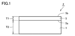
- FIG. 1 is a schematic cross-sectional view of a joined body according to an embodiment of the present disclosure.
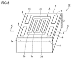
- FIG. 2 is a perspective view showing an example of a bonded substrate having electrodes formed on the main surface of the bonded body of FIG.
- FIG. 3 is a sectional view of the bonded substrate of FIG. 2 taken along line XX.
- FIG. 4 is a schematic cross-sectional view of a surface acoustic wave device according to an embodiment of the present disclosure.
- an object of the present invention is to provide a bonded body that includes a support substrate that has low cost and appropriate strength, and that can suppress loss of elastic waves, and a surface acoustic wave device including the bonded body. To do.
- a bonded body according to an aspect of the present disclosure includes a piezoelectric substrate and a spinel polycrystalline substrate provided on one main surface of the piezoelectric substrate,
- the spinel polycrystalline substrate is a bonded body having a porosity of 0.005% or more and 0.6% or less.
- the bonded body includes the support substrate having appropriate strength at low cost, and the loss of elastic waves can be suppressed.
- the spinel polycrystalline substrate includes a plurality of crystal grains,
- the crystal grains preferably have an average grain size of more than 1 ⁇ m and 60 ⁇ m or less.
- the spinel polycrystalline substrate includes a plurality of crystal grains,
- the crystal grains preferably have an average grain size of 5 ⁇ m or more and 30 ⁇ m or less.
- the piezoelectric substrate is preferably made of lithium tantalate or lithium niobate. According to this, the electromechanical coupling coefficient of the piezoelectric substrate can be increased, and the frequency filter characteristic of the piezoelectric substrate can be improved.
- a surface acoustic wave device includes the bonded body according to any one of (1) to (4) above.
- a surface acoustic wave device comprising: an electrode provided on a main surface of the piezoelectric substrate opposite to a surface provided with the spinel polycrystalline substrate.
- the surface acoustic wave device can suppress the loss of the acoustic wave.
- the same reference numerals represent the same or corresponding parts.
- the dimensional relationships such as length, width, thickness, and depth are appropriately changed for the sake of clarity and simplification of the drawings, and do not necessarily represent actual dimensional relationships.
- the notation in the form of “AB” means the upper and lower limits of the range (that is, A or more and B or less), and when A has no unit, B only has a unit.
- the unit of B and the unit of B are the same.
- the upper limit of the range being C means that the upper limit of the range is C or lower
- the lower limit of the range being D means that the lower limit of the range is D or higher.
- the joined body according to this embodiment will be described with reference to FIG.
- the bonded body 2 according to this embodiment is on a piezoelectric substrate 5 and one main surface (hereinafter, also referred to as “first main surface”) 5a of the piezoelectric substrate 5.
- the spinel polycrystal substrate 1 provided in 1. has a porosity of 0.005% or more and 0.6% or less.
- the inventors of the present invention have made a bonded body including a piezoelectric substrate and a spinel polycrystalline substrate provided on one main surface of the piezoelectric substrate, the pores of the spinel polycrystalline substrate. It has been newly found that the bonded body having a rate of 0.005% or more and 0.6% or less includes a supporting substrate having appropriate strength at low cost and can suppress elastic wave loss. The reason for this is not clear, but it is presumed to be as follows (i) to (iv).
- the bonded body according to the present embodiment uses a spinel polycrystalline substrate as a supporting substrate.
- the spinel polycrystalline substrate is made of a spinel sintered body and has an appropriate strength as a supporting substrate. Further, the material itself of the spinel polycrystalline substrate is cheaper than the single crystal substrate of sapphire or silicon. Further, the spinel polycrystalline substrate has a smaller Knoop hardness than sapphire, can be easily processed into a desired shape, and can reduce the manufacturing cost.
- the elastic wave propagating through a substance is divided into a transmitted wave and a reflected wave at a boundary between solids made of different substances (for example, a boundary between a piezoelectric substrate and a spinel polycrystalline substrate), but a solid wave and a gas At the interface, most of it becomes a reflected wave.
- the spinel polycrystalline substrate used for the bonded body according to the present embodiment has pores inside. Therefore, most of the elastic wave propagating from the piezoelectric substrate to the spinel polycrystalline substrate becomes a reflected wave at the interface between the spinel sintered body and the pores inside the spinel polycrystalline substrate, and returns to the piezoelectric substrate side. .. Therefore, the loss of elastic waves can be suppressed.
- the pores in the spinel polycrystalline substrate are taken in by the grain boundaries between spinel particles during the sintering process during the production of the spinel sintered body, or are taken into the grains during grain growth.
- the pores are dispersed in the spinel polycrystalline substrate without being unevenly distributed. Therefore, a uniform elastic wave reflection effect can be obtained in the entire spinel polycrystalline substrate, and elastic wave loss can be suppressed.
- the spinel polycrystalline substrate has a porosity of 0.005% or more and 0.6% or less. According to this, the spinel polycrystalline substrate has an excellent effect of reflecting elastic waves, an effect of suppressing thermal expansion of the piezoelectric substrate, and a sufficient bonding strength with the piezoelectric substrate while maintaining an appropriate strength. You can
- the porosity of the spinel polycrystalline substrate is less than 0.005%, it tends to be difficult to obtain the elastic wave reflection effect due to the pores.
- the porosity exceeds 0.6%, the reflection effect increases, but the elastic modulus decreases, so that it tends to be difficult to obtain the effect as a supporting substrate of suppressing the thermal expansion of the piezoelectric substrate.
- the porosity exceeds 0.6%, the contact area at the bonding interface between the spinel polycrystalline substrate and the piezoelectric substrate decreases, and the bonding strength tends to decrease.
- the average thickness of the bonded body 2 is preferably 50 ⁇ m or more and 700 ⁇ m or less, more preferably 80 ⁇ m or more and 500 ⁇ m or less, and further preferably 100 ⁇ m or more and 300 ⁇ m or less.
- the thickness of the bonded body is a value measured by a micrometer in a cross section parallel to the normal direction of the main surface of the bonded body. The measurement is performed at three points on one cross section, and the average value of the three points is taken as the average thickness of the bonded body.
- the main surface of the bonded body includes the surface 5b of the piezoelectric substrate and the surface of the spinel polycrystalline substrate, but in the present specification, the main surface of the bonded body means the surface 5b of the piezoelectric substrate. Shall be shown.
- the shape and size of the main surface of the bonded body 2 are not particularly limited, and can be appropriately adjusted depending on the application of the surface acoustic wave device.
- the main surface of the bonded body 2 may be circular or rectangular, for example.
- the diameter can be 50 mm or more and 200 mm or less.
- the length of one side thereof can be set to 0.1 mm or more and 5 mm or less.
- the area of the main surface of the bonded body can be, for example, 0.01 mm 2 or more and 25 mm 2 or less.
- the method of joining the piezoelectric substrate 5 and the spinel polycrystalline substrate 1 is not particularly limited, and an adhesive may be used, or the van der Waals force may be used for joining.
- an adhesive may be used, or the van der Waals force may be used for joining.
- the piezoelectric substrate and the spinel polycrystalline substrate be bonded by Van der Waals force. More specifically, it is preferable that the atoms of the material forming the piezoelectric substrate and the atoms of the spinel forming the spinel polycrystalline substrate are joined by Van der Waals force.
- the piezoelectric substrate 5 is a substrate having a piezoelectric effect of converting an electric signal into mechanical vibration.
- the main component of the piezoelectric substrate 5 for example, lithium tantalate, lithium niobate, lithium borate or the like can be used. Among these, lithium tantalate or lithium niobate, which has an excellent electromechanical coupling coefficient, is preferable.
- the piezoelectric substrate 5 can be obtained, for example, by producing a single crystal ingot of the above-mentioned component by the Czochralski method and slicing this.
- the substrate orientation (cut angle) can be, for example, 36° to 50°, and can be appropriately selected according to the application of the surface acoustic wave device.
- the lower limit of the average thickness T1 of the piezoelectric substrate 5 is preferably 0.1 ⁇ m, more preferably 1 ⁇ m, even more preferably 3 ⁇ m.
- the upper limit of the average thickness T1 of the piezoelectric substrate 5 is preferably 50 ⁇ m, more preferably 25 ⁇ m, even more preferably 10 ⁇ m.
- the average thickness T1 of the piezoelectric substrate 5 is preferably 0.1 ⁇ m or more and 50 ⁇ m or less, more preferably 1 ⁇ m or more and 25 ⁇ m or less, and further preferably 3 ⁇ m or more and 10 ⁇ m or less.
- the thickness of the piezoelectric substrate is a value measured by observing a cross section parallel to the normal line direction of the second main surface 5b of the piezoelectric substrate by a reflection spectral interference method. The measurement is performed at three points on one cross section, and the average value of the three points is taken as the average thickness of the piezoelectric substrate.
- the upper limit of the arithmetic average roughness (Ra) of the first main surface 5a of the piezoelectric substrate 5 is preferably 1 nm, more preferably 0.8 nm. If the arithmetic average roughness (Ra) of the first main surface 5a of the piezoelectric substrate 5 exceeds 1 nm, the adhesive strength with the spinel polycrystalline substrate 1 due to Van der Waals force may be reduced. On the other hand, the lower limit of the arithmetic average roughness (Ra) of the first main surface 5a of the piezoelectric substrate 5 is preferably 0.05 nm.
- the arithmetic mean roughness means the arithmetic mean roughness defined in JIS B 0601.
- the arithmetic mean roughness is a value measured by an atomic force microscope (AFM: Atomic Force Microscope) or the like.
- the upper limit of the linear expansion coefficient of the piezoelectric substrate 5 is preferably 30 ⁇ 10 ⁇ 6 /° C., more preferably 20 ⁇ 10 ⁇ 6 /° C. When the coefficient of linear expansion of the piezoelectric substrate 5 exceeds 30 ⁇ 10 ⁇ 6 /° C., the expansion or contraction of the piezoelectric substrate due to the temperature change may increase.
- the lower limit of the linear expansion coefficient of the piezoelectric substrate 5 is not particularly limited, but for example, 8 ⁇ 10 ⁇ 6 /° C. is preferable, and 10 ⁇ 10 ⁇ 6 is more preferable.
- the above-mentioned linear expansion coefficient is a value measured by the compression load method ("Thermo-mechanical analyzer TMA8310" manufactured by Rigaku Corporation).
- the piezoelectric substrate 5 may include a component other than the above main components, and for example, a metal or the like may be added.
- the mechanical strength and heat resistance of the piezoelectric substrate 5 can be improved by adding the metal element.
- the spinel polycrystalline substrate 1 is a substrate made of a spinel sintered body.
- the spinel polycrystalline substrate 1 is a supporting base material for increasing the strength of the bonded body 2 and suppressing thermal expansion of the piezoelectric substrate.
- Examples of spinel that constitutes the spinel polycrystalline substrate 1 include MgO.nAl 2 O 3 (1 ⁇ n ⁇ 3).
- the lower limit of the value of n is preferably 1, more preferably 1.03, further preferably 1.05. When the value of n is less than 1, MgO locally increases and the porosity tends to increase.
- the upper limit of the value of n is preferably 3, more preferably 2, and even more preferably 1.5.
- n is preferably 1 or more and 3 or less, more preferably 1.03 or more and 2 or less, still more preferably 1.05 or more and 1.5 or less.
- composition of the spinel polycrystalline substrate and the value of n in the composition formula MgO.nAl 2 O 3 can be measured by the X-ray diffraction matrix flushing method.
- the spinel polycrystalline substrate 1 may include a component other than spinel, and can include, for example, an alumina component.
- the upper limit of the content of components other than spinel in the spinel polycrystalline substrate is preferably 10% by mass, and more preferably 5% by mass.
- the lower limit of the content of components other than spinel in the spinel polycrystalline substrate is preferably 3% by mass, more preferably 1% by mass, and 0, that is, it is even more preferable that no components other than spinel are contained.
- the spinel polycrystalline substrate 1 has a porosity of 0.005% or more and 0.6% or less.
- the lower limit of the porosity is 0.005%, preferably 0.01%, and more preferably 0.05%. If the lower limit of the porosity is less than 0.005%, it tends to be difficult to obtain the elastic wave reflection effect of the pores.
- the upper limit of the porosity is 0.6%, preferably 0.5%. When the porosity exceeds 0.6%, the reflection effect is enhanced, but the elastic modulus is lowered, so that it tends to be difficult to obtain the effect as a support substrate of suppressing the thermal expansion of the piezoelectric substrate.
- the porosity of the spinel polycrystalline substrate is 0.005% or more and 0.6% or less, preferably 0.01% or more and 0.6% or less, more preferably 0.01% or more and 0.5% or less, and 0 It is more preferably 0.05% or more and 0.5% or less.
- the porosity of the spinel polycrystalline substrate is measured by the water immersion method.
- the specific procedure of the water immersion method is as follows (a1) to (a3).
- a spinel polycrystalline substrate is cut into a cylinder with a size of ⁇ 100 mm ⁇ 40 mm to obtain a measurement sample.
- (A2) Immerse the measurement sample in water and obtain the apparent volume of the measurement sample according to Archimedes' principle.
- the apparent density ( ⁇ ) is obtained from the ratio of the apparent volume and the mass of the measurement sample.
- An electronic balance (“UX200H” manufactured by SHIMADZU) is used for measuring the apparent volume.
- Porosity ( ⁇ ) (%) (1- ⁇ / ⁇ 0 ) ⁇ 100
- the pores are dispersed. According to this, it is possible to obtain a uniform elastic wave reflection effect over the entire spinel polycrystalline substrate, and to suppress elastic wave loss.
- the presence of dispersed pores in the spinel polycrystalline substrate can be confirmed by visually observing that it does not appear cloudy, and by observing with a SEM (Scanning Electron Microscope, scanning electron microscope).
- the pores in the spinel polycrystalline substrate are taken in at the grain boundaries between spinel particles or in the grains during grain growth in the sintering step during the production of the spinel sintered body. The pores are dispersed in the spinel polycrystalline substrate without being unevenly distributed. Therefore, the spinel polycrystalline substrate does not require expensive fine processing and is advantageous in cost.
- the shape of the pores in the spinel polycrystalline substrate approaches the most stable spherical shape during crystal growth.
- the shape of the pores does not have to be a perfect sphere.
- the projected area of the pore in the traveling direction of the elastic wave is stable and wide.
- the ratio of the minimum diameter to the maximum diameter is 80% or more because the effect of confining the elastic wave is further improved.
- the shape of the pores can be confirmed by SEM.
- the pores in the spinel polycrystalline substrate have an average diameter of 0.01 ⁇ m or more and 20 ⁇ m or less, more preferably 0.05 ⁇ m or more and 10 ⁇ m or less, further preferably 0.1 ⁇ m or more and 5 ⁇ m or less in a projected image in the traveling direction of the elastic wave of the pores. preferable. If the average diameter is less than 0.01 ⁇ m, the reflection effect may be difficult to appear. On the other hand, when the average diameter exceeds 20 ⁇ m, the pores tend to be unevenly distributed in the spinel polycrystalline substrate, and it is difficult to obtain a uniform elastic wave confining effect.
- the average diameter in the projected image of the pores in the traveling direction of the elastic wave means the median diameter (d50) in the volume-based particle size distribution (volume distribution), and all the pores included in the spinel polycrystalline substrate are targeted. It means that the average particle diameter.
- the diameter of each pore for calculating the average diameter of the pores can be measured using SEM. As long as the measurement is carried out by the applicant, as long as it is measured in the same sample, even if the average diameter of the pores is calculated multiple times by changing the selected part of the measurement field of view, there is almost no variation in the calculation results, and it is arbitrary. It was confirmed that the setting of the measurement field of view should not be arbitrary.
- the spinel polycrystalline substrate includes a plurality of crystal grains, and the crystal grains preferably have an average grain size of more than 1 ⁇ m and 60 ⁇ m or less. According to this, the loss of elastic waves can be suppressed more effectively.
- the average grain size of the crystal grains is 1 ⁇ m or less, the porosity of the spinel polycrystalline substrate becomes too large and the elastic modulus decreases, so it is difficult to obtain the effect as a supporting substrate of suppressing the thermal expansion of the piezoelectric substrate. Tend. Furthermore, since the contact area at the bonding interface between the spinel polycrystalline substrate and the piezoelectric substrate is reduced, the bonding strength is reduced. On the other hand, when the average grain size of the crystal grains exceeds 60 ⁇ m, pores existing at grain boundaries between spinel grains tend to be unevenly distributed.
- the average grain size of the spinel polycrystalline substrate is more preferably 5 ⁇ m or more and 30 ⁇ m or less, and further preferably 8 ⁇ m or more and 25 ⁇ m or less.
- the particle size of each particle for calculating the average particle size of crystal particles can be measured by the following method. First, the surface of the spinel polycrystalline substrate is mirror-polished, and a 0.17 mm ⁇ 0.13 mm rectangular measurement visual field is determined on the polished surface. The spinel polycrystalline substrate in the measurement visual field is observed with an optical microscope at a magnification of 1000 times. Next, in this optical microscope image, the number of each crystal grain forming the spinel polycrystalline substrate is counted, and the value obtained by dividing the measurement visual field area by the number of crystal grains is taken as the grain size of the crystal grains.
- the lower limit of the average thickness T2 of the spinel polycrystalline substrate 1 is preferably 100 ⁇ m, more preferably 150 ⁇ m, even more preferably 200 ⁇ m.
- the upper limit of the average thickness T2 of the spinel polycrystalline substrate 1 is preferably 500 ⁇ m, more preferably 400 ⁇ m, even more preferably 300 ⁇ m.
- the average thickness T2 of the spinel polycrystalline substrate 1 exceeds 500 ⁇ m, bulk waves may be easily reflected at the boundary between the piezoelectric substrate 5 and the spinel polycrystalline substrate 1, and the bonded body 2 may be unnecessarily thick. is there.
- the thickness of the above spinel polycrystalline substrate is a value measured by observing a cross section parallel to the normal line direction of the main surface of the spinel polycrystalline substrate by reflection interference spectroscopy. The measurement is performed at three points in one cross section, and the average value of the three points is taken as the average thickness of the spinel polycrystalline substrate.
- the ratio T1/T2 which is the ratio between the average thickness T1 of the piezoelectric substrate 5 and the average thickness T2 of the spinel polycrystalline substrate 1, is 0.1 or less, and the ratio of the average thickness T1 of the piezoelectric substrate to the spinel polycrystalline substrate is The average thickness T2 is sufficiently large. Therefore, the spinel polycrystalline substrate can sufficiently suppress thermal expansion of the piezoelectric substrate, and the bonded body can have excellent frequency-temperature characteristics with little variation.
- the upper limit of the ratio T1/T2 is 0.1, preferably 0.04, more preferably 0.02.
- T1/T2 exceeds 0.1, the frequency temperature characteristic (TCF) tends to deteriorate.
- the lower limit of the ratio T1/T2 is preferably 0.0002, more preferably 0.002, and even more preferably 0.006. If the ratio T1/T2 is less than 0.0002, the processing accuracy of the piezoelectric substrate 5 may decrease. Further, there is a risk that the deformation of the bonded body 2 due to a temperature change will increase or that the mechanical strength will decrease.
- the lower limit of the arithmetic mean roughness (Ra) of the surface of the spinel polycrystalline substrate 1 is preferably 0.01 nm, more preferably 0.1 nm.
- the arithmetic average roughness (Ra) of the surface of the spinel polycrystalline substrate 1 is less than 0.01 nm, it is necessary to process the surface of the spinel polycrystalline substrate 1 to be extremely flat, which increases the processing cost.
- the upper limit of the arithmetic average roughness (Ra) of the surface of the spinel polycrystalline substrate 1 is preferably 3.0 nm, more preferably 2.0 nm.
- the upper limit of the linear expansion coefficient of the spinel polycrystalline substrate 1 is preferably 16 ⁇ 10 ⁇ 6 /° C., more preferably 8 ⁇ 10 ⁇ 6 /° C. If the linear expansion coefficient of the spinel polycrystalline substrate 1 exceeds 16 ⁇ 10 ⁇ 6 /° C., the thermal expansion of the piezoelectric substrate may not be sufficiently suppressed.
- the lower limit of the linear expansion coefficient of the spinel polycrystalline substrate 1 is preferably 1 ⁇ 10 ⁇ 6 /° C., more preferably 3 ⁇ 10 ⁇ 6 /° C.
- the linear expansion coefficient of the spinel polycrystalline substrate 1 is less than 1 ⁇ 10 ⁇ 6 /° C., the difference between the linear expansion coefficient of the spinel polycrystalline substrate 1 and that of the piezoelectric substrate 5 becomes large, and the strain of the spinel polycrystalline substrate 1 may increase when the temperature changes. is there.
- the above-mentioned linear expansion coefficient is a value obtained by measuring a rod-shaped material with a linear thermal expansion measuring device.
- the lower limit of the difference in linear expansion coefficient between the spinel polycrystalline substrate 1 and the piezoelectric substrate 5 is preferably 5 ⁇ 10 ⁇ 6 /° C., more preferably 7 ⁇ 10 ⁇ 6 /° C. If the difference in linear expansion coefficient between the spinel polycrystalline substrate 1 and the piezoelectric substrate 5 is less than 5 ⁇ 10 ⁇ 6 /° C., the thermal expansion of the piezoelectric substrate may not be sufficiently suppressed.
- the upper limit of the difference in linear expansion coefficient between the spinel polycrystalline substrate 1 and the piezoelectric substrate 5 is preferably 20 ⁇ 10 ⁇ 6 /°C. When the difference in linear expansion coefficient between the spinel polycrystalline substrate 1 and the piezoelectric substrate 5 exceeds 20 ⁇ 10 ⁇ 6 /° C., the strain of the spinel polycrystalline substrate 1 may increase when the temperature changes.
- the spinel polycrystalline substrate 1 supports a piezoelectric substrate 5 that vibrates when receiving an electric signal. Therefore, considerable stress is applied to the spinel polycrystalline substrate 1.
- the piezoelectric substrate 5 When the piezoelectric substrate 5 is activated, the piezoelectric substrate 5 generates heat, and the heat is also propagated to the spinel polycrystalline substrate 1. At this time, thermal stress is generated in the spinel polycrystalline substrate 1. For this reason, the spinel polycrystalline substrate 1 preferably has a corresponding strength.
- the lower limit of the Young's modulus of the spinel polycrystalline substrate 1 is preferably 100 GPa, more preferably 150 GPa, even more preferably 180 GPa. If the Young's modulus of the spinel polycrystalline substrate 1 is less than 100 GPa, the spinel polycrystalline substrate 1 may be easily cracked.
- the upper limit of the Young's modulus of the spinel polycrystalline substrate 1 is preferably 400 GPa, more preferably 350 GPa, further preferably 300 GPa. If the Young's modulus of the spinel polycrystalline substrate 1 exceeds 400 GPa, the hardness of the spinel polycrystalline substrate 1 becomes excessively high, so that chipping is likely to occur. Further, since the hardness of the spinel polycrystalline substrate 1 becomes excessively high, it may be difficult to process it.
- the Young's modulus is a value measured by a three-point bending test performed according to JIS R 1602.
- a “Material Testing Machine AL-50NB” manufactured by Minebea Co., Ltd. is used for the measurement.
- the lower limit of the Knoop hardness of the spinel polycrystalline substrate 1 is preferably 1000, more preferably 1200. If the Knoop hardness of the spinel polycrystalline substrate 1 is less than 1000, the spinel polycrystalline substrate 1 may be easily cracked.
- the upper limit of the Knoop hardness of the spinel polycrystalline substrate 1 is preferably 2500 and more preferably 1800. If the Knoop hardness of the spinel polycrystalline substrate 1 exceeds 2500, it may be difficult to process the spinel polycrystalline substrate 1.
- Knoop hardness is a value measured by "Hardness Testing Machine HM” manufactured by Mitutoyo Corporation.
- the method for manufacturing a bonded body according to the present embodiment includes a step of preparing a piezoelectric substrate, a step of preparing a spinel polycrystalline substrate, and a step of bonding the piezoelectric substrate and the spinel polycrystalline substrate to obtain a bonded body ( Hereinafter, also referred to as a “joining step”).
- a piezoelectric substrate is prepared.
- a conventionally known piezoelectric substrate can be used as the piezoelectric substrate.
- the main surface of the piezoelectric substrate is polished. Specifically, after the main surface of the piezoelectric substrate is roughly polished by grinding, the arithmetic mean roughness (Ra) is measured by CMP (Chemical Mechanical Polishing) with respect to the surface to which the spinel polycrystalline substrate is bonded. Is reduced to about 0.05 ⁇ m or more and about 1 ⁇ m or less.
- the step of preparing the spinel polycrystalline substrate can include a spinel powder preparation step, a forming step, a sintering step, and a processing step.
- a powder having a composition formula of MgO.nAl 2 O 3 (1 ⁇ n ⁇ 3) and made of spinel is prepared.
- the spinel powder preferably has an average particle size of 0.1 ⁇ m or more and 0.3 ⁇ m or less and a purity of 99.5% or more.
- the mixing ratio (mass ratio) of MgO (magnesium oxide) powder and Al 2 O 3 (alumina) powder is 1 ⁇ Al 2 O 3 /MgO ⁇ 3. It is preferable to mix them.
- the particle size of each particle to calculate the average particle size of the spinel powder is measured using the particle size distribution measurement method by the laser diffraction/scattering method. Specifically, it is a method of measuring the diameter of the powder particles by analyzing the scattered intensity distribution of the scattered light of the laser light irradiated on the powder particles.
- a molding process is performed. Specifically, a molded body is obtained by molding by press molding or CIP (Cold Isostatic Pressing). More specifically, it is preferable that the MgO.nAl 2 O 3 powder prepared in the spinel powder preparation step be first preformed by press forming and then CIP to obtain a formed body. Note that either one of press molding and CIP may be performed, or both may be performed, for example, CIP is performed after press molding.
- a pressure of 1 MPa or more and 300 MPa or less, particularly 10 MPa or more and 100 MPa or less is preferably used.
- CIP for example, it is preferable to use a pressure of 160 MPa or more and 250 MPa or less, particularly 180 MPa or more and 230 MPa or less.
- the molded body is sintered in a vacuum under a temperature condition of 1500° C. or higher and 1700° C. or lower (first sintering step), and then by HIP (Hot Isostatic Pressing). Under a temperature condition of 1600° C. or more and 1800° C. or less, sintering is performed while changing the pressure in multiple stages (second sintering process). Thereby, a spinel ingot made of a spinel sintered body having a porosity of 0.005% or more and 0.6% or less can be obtained.
- the second sintering step is a second a sintering step of sintering at a pressure of 100 MPa to 200 MPa under a temperature condition of 1600° C. to 1800° C. for 1 minute to 60 minutes, It is preferable to include a second b sintering step of sintering at a pressure of 150 MPa to 300 MPa under a temperature condition of 1600° C. to 1800° C. for 10 minutes to 300 minutes.
- the processing process Specifically, the obtained spinel ingot is sliced with a diamond wire saw so as to have a desired thickness. As a result, the base of the spinel polycrystalline substrate having a desired thickness is completed.
- the desired thickness is preferably determined in consideration of the thickness of the spinel polycrystalline substrate to be finally formed and the amount of polishing of the main surface of the spinel polycrystalline substrate in the subsequent step.
- the main surface of the spinel polycrystalline substrate is polished. Specifically, after the main surface of the spinel polycrystalline substrate is roughly polished by grinding, the surface to which the piezoelectric substrate is finally bonded is subjected to arithmetic mean roughness (CMP (Chemical Mechanical Polishing) by CMP (Chemical Mechanical Polishing). The surface roughness is reduced until Ra) is about 0.01 nm or more and 3.0 nm or less. As a result, the spinel polycrystalline substrate can be bonded to the main surface of the piezoelectric substrate by Van der Waals force.
- CMP Chemical Mechanical Polishing
- CMP Chemical Mechanical Polishing
- the piezoelectric substrate prepared above and the spinel polycrystalline substrate are bonded to obtain a bonded body.
- the polishing surface of the spinel polycrystalline substrate and the polishing surface of the piezoelectric substrate face each other and are placed in the vacuum chamber. While maintaining this state, the internal gas in the chamber is exhausted to a high vacuum state. After that, the polished surfaces of both substrates are irradiated with a high-speed atom beam of neutralized argon, and then both substrates are brought into close proximity to each other to obtain a joined body.
- the surface acoustic wave device 10 is a surface on which the bonded body 2 described in the first embodiment and the spinel polycrystalline substrate 1 of the piezoelectric substrate 5 are provided.
- the electrode 3 is provided on the main surface (second main surface 5b) opposite to the (first main surface 5a).
- the bonded body 2 includes a piezoelectric substrate 5 and a spinel polycrystalline substrate provided on one main surface (first main surface 5a) of the piezoelectric substrate 5.
- the configurations of the bonded body, the piezoelectric substrate, and the spinel polycrystalline substrate used in this embodiment are the same as the configurations described in the first embodiment, and therefore the description thereof will not be repeated.
- the electrode 3 can include a first pole 3a and a second pole 3b. For example, an AC voltage is applied between the first pole 3a and the second pole 3b. Then, an electric signal is input to the current generated by the alternating voltage applied between the first pole 3a and the second pole 3b. Then, the crystal grains (atoms) forming the piezoelectric substrate 5 provided with the electrodes 3 are subjected to stress to approach or leave each other due to the piezoelectric effect, so that the main surface of the piezoelectric substrate 5 vibrates in a wavy manner.
- the first pole 3a and the second pole 3b can each have a comb shape. According to this, for example, among the electric signals input to the electrode 3, only the electric signal having a wavelength corresponding to the distance between the comb-shaped component 3c and the comb-shaped component 3d of the first pole 3a is propagated to the outside. That is, an electric signal having a wavelength other than the above-mentioned wavelength is not propagated to the outside and is blocked inside the bonded body 2.
- the bonded body 2 outputs only an electric signal having a desired wavelength to the outside, thereby blocking an electric signal (that is, noise) other than the desired wavelength and eliminating noise in the output signal. it can.
- an electrode member 6 can be further provided on the second main surface 5b of the piezoelectric substrate.
- the piezoelectric substrate 5, the electrode 3 provided on the second main surface 5b of the piezoelectric substrate, and the first main surface 5a of the piezoelectric substrate are formed on the piezoelectric substrate 5.
- the joined spinel polycrystalline substrate 1 forms a joined substrate 4.
- the bonding substrate 4 can further include the first electrode member 6.
- the surface acoustic wave device may be formed of only the bonding substrate 4, or may include other components in addition to the bonding substrate 4 as described below.
- An example in which the surface acoustic wave device includes another structure in addition to the bonded substrate 4 will be described with reference to FIG.
- the surface acoustic wave device 410 can further include a sealing substrate 7 for sealing the electrode 3 in addition to the bonding substrate 4.
- the second electrode member 9 made of a metal thin film is formed on the main surface of the sealing substrate 7 facing the bonding substrate 4, and the external terminals 11 are formed on the other main surface.
- the second electrode member 9 and the external terminal 11 are electrically connected via a via wiring 8 penetrating the sealing substrate 7.
- the first electrode member 6 and the second electrode member 9 are arranged so as to be in contact with each other, the first electrode member 6 and the external terminal 11 are also connected to the second electrode member 9 And are electrically connected via the via wiring 8.
- the bonding substrate 4 and the sealing substrate 7 are bonded via the adhesive member 13.
- the adhesive member 13 is provided so as to surround the electrode 3, the first electrode member 6, and the second electrode member 9. Therefore, the electrode 3, the first electrode member, and the second electrode member are shielded from the outside and hermetically sealed.
- the bonding substrate 4 and the sealing substrate 7 may be directly bonded by pressure bonding without using an adhesive member.
- metal or resin can be used as the adhesive member 13.
- metal gold, platinum, silver, copper, aluminum, nickel, titanium, gold alloy, a metal whose surface is coated with gold, or the like can be used.
- resin an epoxy resin, an acrylic resin, a silicone resin, a polyimide resin, a polyamide resin, a polyamideimide resin, or the like can be used.
- the average thickness of the sealing substrate 7 is preferably 10 ⁇ m or more and 1000 ⁇ m or less.
- the thickness of the surface acoustic wave device 410 is preferably 50 ⁇ m or more and 300 ⁇ m or less.
- the main surface of the surface acoustic wave device 10 is preferably a rectangle whose one side length is 0.1 mm or more and 10 mm or less.
- the method for manufacturing a surface acoustic wave device includes a step of preparing a bonding substrate, a step of preparing a sealing substrate, and a step of bonding the bonding substrate and the sealing substrate to obtain a surface acoustic wave device. Can be provided.
- a bonded substrate is prepared.
- the bonded substrate can be obtained by forming electrodes on the main surface of the bonded body described in the first embodiment. Specifically, first, the piezoelectric substrate 5 in the bonded body 2 is thinned by polishing, and then the surface is cleaned by RCA cleaning. Next, an aluminum-based material to be an electrode is deposited on the polished surface of the piezoelectric substrate 5 by electron beam evaporation to a thickness of 100 to several hundred ⁇ .
- the RIE (Reactive Ion Etching) device removes the aluminum-based material that is not masked by the resist, leaving the aluminum-based material only in the electrode portion.
- the resist is removed to complete the electrode.
- the piezoelectric substrate 5, the electrode 3 provided on the second main surface 5b of the piezoelectric substrate 5, and the spinel polycrystalline substrate 1 bonded to the first main surface 5a of the piezoelectric substrate 5 are formed. It is possible to obtain the bonded substrate 4 including and.
- the first electrode member 6 can also be formed on the second main surface 5b of the piezoelectric substrate 5 by the same method as the method for producing the electrode 3 described above.
- the bonded substrate obtained above corresponds to the surface acoustic wave device 10.
- the following steps are further performed.
- the sealing substrate 7 for example, a substrate made of spinel is prepared. Via wirings 8 penetrating the substrate are formed on the substrate. Next, a second electrode member 9 is formed on one main surface of the substrate so as to cover the via wiring 8. Further, an external terminal 11 is formed on the other main surface of the substrate so as to cover the via wiring 8. Thereby, the sealing substrate 7 can be obtained.
- the obtained bonded substrate 4 and the sealing substrate 7 are bonded.
- the adhesive member 13 made of metal or resin is arranged on the second main surface 5b of the piezoelectric substrate 5.
- the sealing substrate 7 is arranged so as to face the second main surface 5b of the piezoelectric substrate 5.
- the first electrode member 6 and the second electrode member 9 are arranged so as to be in contact with each other.
- the sealing substrate 7 is pressed against the piezoelectric substrate 5 at a constant heating temperature, the sealing substrate 7 and the piezoelectric substrate 5 are bonded with the adhesive member 13, and the electrode 3 is hermetically sealed.
- the surface acoustic wave device 410 can be obtained by cutting the bonding substrate 4 and the sealing substrate 7 into a desired size while keeping the electrodes 3 hermetically sealed. Further, the surface acoustic wave device 410 may be obtained by cutting the bonded substrate 4 into a desired size and bonding it to the sealing substrate 7.
- the porosity is 0.0%, 0.002%, 0.005%, 0.1%, 0.2%, 0.3%, 0.5%, 0.6%, 0.8% and In the case of 1.0%, the projected surface coverage of the pores on the plane parallel to the surface of the spinel polycrystalline substrate was calculated by the following formula (1).
- Projection surface coverage (porosity) 2/3 (1)
- shape of the pores was assumed to be a true sphere.
- results are shown in the column of "projection surface coverage" in Table 1.
- the spinel sintered body that constitutes the spinel polycrystalline substrate is generally treated as an isotropic material because the macroscopic grain orientation is not uniform.
- the grain size of each crystal particle forming the spinel sintered body is about several tens of ⁇ m, even if the spinel sintered body has the same density, the velocity of the elastic wave depends on the direction. (Sound velocity) has anisotropy. Assuming that the velocity (sound velocity) of the elastic wave of the crystal A is 3900 m/sec and the velocity (sound velocity) of the elastic wave of the crystal B is 3500 m/sec, the reflection at the boundary (grain boundary) of the acoustic impedance is 5. It will be about 4%.
- the lower the porosity the higher the strength of the surface acoustic wave device. From the above results, when the bubble ratio is 0.005% or more, the elastic wave confinement effect can be obtained, so that the loss of the elastic wave can be suppressed, and when the porosity is 0.6% or less, the spinel It can be seen that the decrease in strength of the polycrystalline substrate can be suppressed within 3%.
- the projected pore diameters are 0.04 ⁇ m, 0.18 ⁇ m, 0.74 ⁇ m, 1.11 ⁇ m, 2.21 ⁇ m, and 2.95 ⁇ m, respectively.
- the projected pore diameters are 0.18 ⁇ m, 0.9 ⁇ m, 3.6 ⁇ m, 5.4 ⁇ m, 10.9 ⁇ m, and 14.5 ⁇ m, respectively.
- the average grain size of the crystal grains contained in the spinel polycrystalline substrate is 1 ⁇ m or less, the difference from the average grain size of the spinel powder which is a starting material becomes small, so that the porosity is increased in the sintering process. It was confirmed that it was difficult to lower it sufficiently.
- the average grain size of the crystal grains contained in the spinel polycrystalline substrate is preferably 5 ⁇ m or more.
- the average crystal grain size of the crystal grains contained in the spinel polycrystalline substrate is larger than 60 ⁇ m, there are actually grains having a grain size of 90 ⁇ m or more, and the pores existing in that portion are large, which increases the material strength. It was confirmed that there is a tendency to significantly lower locally.
- the average grain size of the crystal grains contained in the spinel polycrystalline substrate is preferably 30 ⁇ m or less.
- (Average quality factor) 1-port resonator electrodes were arranged in a grid pattern on a 4-inch diameter bonded substrate. The substrate was cut by dicing so that the resonator electrodes were arranged on each piece, a probe connected to a network analyzer was applied to the electrodes, and the impedance was measured while changing the frequency.
- the values of L, C, and R were calculated by the least-squares method simulation of the equivalent circuit according to the states of the resonance and anti-resonance peaks, and the quality factor Q value was derived.
- the average value was calculated from the quality factor Q value derived from a total of 10 resonator electrodes, each of which was two in the center of the wafer and in the vicinity of five points in the upper, lower, left and right directions.
- the average grain size of the crystal grains contained in the spinel polycrystalline substrate is particularly preferably 5 ⁇ m or more and 30 ⁇ m or less.
Landscapes
- Chemical & Material Sciences (AREA)
- Engineering & Computer Science (AREA)
- Physics & Mathematics (AREA)
- Acoustics & Sound (AREA)
- Ceramic Engineering (AREA)
- Materials Engineering (AREA)
- Manufacturing & Machinery (AREA)
- Structural Engineering (AREA)
- Organic Chemistry (AREA)
- Inorganic Chemistry (AREA)
- Surface Acoustic Wave Elements And Circuit Networks Thereof (AREA)
Abstract
圧電体基板と、前記圧電体基板の一方の主面上に設けられたスピネル多結晶基板とを備え、前記スピネル多結晶基板は、気孔率が0.005%以上0.6%以下である、接合体である。
Description
本開示は、接合体及び表面弾性波デバイスに関する。
携帯電話の内部には、電気信号のノイズをカットし、所望の周波数の電気信号のみを送受信するための、SAW(Surface Acoustic Wave、表面弾性波)フィルタと呼ばれる電子部品が組み込まれている。SAWフィルタには、圧電効果を有する材料からなる圧電体基板を用いる。
圧電体基板の一方の表面には、透過周波数帯の波長に応じたピッチの櫛形電極が形成されている。櫛形電極に入力された電気信号により圧電体基板が応力を受けて変形し、ピッチに応じた弾性波が発生する。又、特定周波数の弾性波を受けて変形した圧電体基板が、櫛形電極に電位を生じさせる。上記の圧電体基板の変形を促進するためには、圧電体基板を薄くすることが効果的である。
SAWフィルタの透過周波数は櫛形電極のピッチで決まる。櫛形電極のピッチは周辺温度の変化による圧電体基板の膨張収縮により変化する。熱膨張による変化を抑制するため、圧電体基板の櫛形電極の形成された表面とは反対側の表面には、高強度かつ低熱膨張である支持基板が貼り付けられている。
特許文献1(特開2006-304206号公報)では、上記の支持基板として、シリコン基板を用いている。シリコンの熱膨張係数は、圧電体基板を形成するタンタル酸リチウム等の材料の熱膨張係数に比べて非常に小さい。従って、圧電体基板が熱により膨張すると、シリコンが割れてしまうおそれがある。
また、上記の支持基板として、サファイヤを用いる技術も提案されている。しかし、サファイヤは単結晶であり、硬度が高いため、小型化のために所望の形状に成形することが困難である。また、シリコンやサファイヤの単結晶基板は一般的に高価であり、より低コストの基板が求められていた。
そこで、特許文献2(特開2011-66818号公報)には、支持基板として、より抵コストで適度な強度を有するスピネルを用いる技術が開示されている。
[1]本開示の一態様に係る接合体は、圧電体基板と、前記圧電体基板の一方の主面上に設けられたスピネル多結晶基板とを備え、
前記スピネル多結晶基板は、気孔率が0.005%以上0.6%以下である、接合体である。
前記スピネル多結晶基板は、気孔率が0.005%以上0.6%以下である、接合体である。
[2]本開示の他の一態様に係る表面弾性波デバイスは、上記[1]に記載の接合体と、
前記圧電体基板の前記スピネル多結晶基板の設けられた面とは反対側の主面上に設けられた電極とを備える、表面弾性波デバイスである。
前記圧電体基板の前記スピネル多結晶基板の設けられた面とは反対側の主面上に設けられた電極とを備える、表面弾性波デバイスである。
[本開示が解決しようとする課題]
電気信号による圧電体基板の変形で発生した弾性波は、圧電体基板表面の面内では、櫛形電極の構造により不要な方向に伝播することを抑制でき、ロスを低減することができる。一方、圧電体基板の厚み方向に伝播する弾性波は、支持基板側に伝播してロスを生じる傾向がある。この傾向は、圧電体基板が薄くなると特に顕著となる。
電気信号による圧電体基板の変形で発生した弾性波は、圧電体基板表面の面内では、櫛形電極の構造により不要な方向に伝播することを抑制でき、ロスを低減することができる。一方、圧電体基板の厚み方向に伝播する弾性波は、支持基板側に伝播してロスを生じる傾向がある。この傾向は、圧電体基板が薄くなると特に顕著となる。
そこで、本目的は、低コストで適度な強度を有する支持基板を備え、弾性波のロスを抑制することのできる接合体、及び、該接合体を備える表面弾性波デバイスを提供することを目的とする。
[本開示の効果]
上記態様によれば、低コストで適度な強度を有する支持基板を備え、弾性波のロスを抑制することのできる接合体、及び、該接合体を備える表面弾性波デバイスを提供することが可能である。
上記態様によれば、低コストで適度な強度を有する支持基板を備え、弾性波のロスを抑制することのできる接合体、及び、該接合体を備える表面弾性波デバイスを提供することが可能である。
[実施形態の概要]
最初に本開示の実施態様を列記して説明する。
最初に本開示の実施態様を列記して説明する。
(1)本開示の一態様に係る接合体は、圧電体基板と、前記圧電体基板の一方の主面上に設けられたスピネル多結晶基板とを備え、
前記スピネル多結晶基板は、気孔率が0.005%以上0.6%以下である、接合体である。
前記スピネル多結晶基板は、気孔率が0.005%以上0.6%以下である、接合体である。
上記態様によれば、接合体は、低コストで適度な強度を有する支持基板を備え、弾性波のロスを抑制することができる。
(2)前記スピネル多結晶基板は複数の結晶粒を含み、
前記結晶粒は、その平均粒径が1μmより大きく60μm以下であることが好ましい。
前記結晶粒は、その平均粒径が1μmより大きく60μm以下であることが好ましい。
これによると、スピネル多結晶基板の強度を維持したまま、弾性波のロスをより効果的に抑制することができる。
(3)前記スピネル多結晶基板は複数の結晶粒を含み、
前記結晶粒は、その平均粒径が5μm以上30μm以下であることが好ましい。
前記結晶粒は、その平均粒径が5μm以上30μm以下であることが好ましい。
これによると、スピネル多結晶基板の強度を維持したまま、弾性波のロスを更に効果的に抑制することができる。
(4)前記圧電体基板はタンタル酸リチウム又はニオブ酸リチウムからなることが好ましい。これによると、圧電体基板の電気機械結合係数を高め、当該圧電体基板の周波数フィルタ特性を向上させることができる。
(5)本開示の他の一態様に係る表面弾性波デバイスは、上記(1)~(4)のいずれかに記載の接合体と、
前記圧電体基板の前記スピネル多結晶基板の設けられた面とは反対側の主面上に設けられた電極とを備える、表面弾性波デバイスである。
前記圧電体基板の前記スピネル多結晶基板の設けられた面とは反対側の主面上に設けられた電極とを備える、表面弾性波デバイスである。
上記態様によれば、表面弾性波デバイスは、弾性波のロスを抑制することができる。
[実施形態の詳細]
本開示の一実施形態に係る接合体及び表面弾性波デバイスの具体例を、以下に図面を参照しつつ説明する。本開示の図面において、同一の参照符号は、同一部分または相当部分を表すものである。また、長さ、幅、厚み、深さ等の寸法関係は図面の明瞭化と簡略化のために適宜変更されており、必ずしも実際の寸法関係を表すものではない。
[実施形態の詳細]
本開示の一実施形態に係る接合体及び表面弾性波デバイスの具体例を、以下に図面を参照しつつ説明する。本開示の図面において、同一の参照符号は、同一部分または相当部分を表すものである。また、長さ、幅、厚み、深さ等の寸法関係は図面の明瞭化と簡略化のために適宜変更されており、必ずしも実際の寸法関係を表すものではない。
本明細書において「A~B」という形式の表記は、範囲の上限下限(すなわちA以上B以下)を意味し、Aにおいて単位の記載がなく、Bにおいてのみ単位が記載されている場合、Aの単位とBの単位とは同じである。また、範囲の上限値がCであるとは、範囲の上限がC以下であることを意味し、範囲の下限値がDであるとは、範囲の下限がD以上であることを意味する。
[実施の形態1:接合体]
<接合体>
本実施形態に係る接合体について、図1を用いて説明する。図1に示されるように、本実施形態に係る接合体2は、圧電体基板5と、該圧電体基板5の一方の主面(以下、「第1の主面」とも記す。)5a上に設けられたスピネル多結晶基板1とを備え、スピネル多結晶基板1は、気孔率が0.005%以上0.6%以下である。
<接合体>
本実施形態に係る接合体について、図1を用いて説明する。図1に示されるように、本実施形態に係る接合体2は、圧電体基板5と、該圧電体基板5の一方の主面(以下、「第1の主面」とも記す。)5a上に設けられたスピネル多結晶基板1とを備え、スピネル多結晶基板1は、気孔率が0.005%以上0.6%以下である。
本発明者らは、鋭意検討の結果、圧電体基板と、該圧電体基板の一方の主面上に設けられたスピネル多結晶基板とを備える接合体であって、該スピネル多結晶基板の気孔率が0.005%以上0.6%以下である接合体は、低コストで適度な強度を有する支持基板を備え、弾性波のロスを抑制することができることを新たに見出した。この理由は明らかではないが、下記(i)~(iv)の通りと推察される。
(i)本実施形態に係る接合体は、支持基板としてスピネル多結晶基板を用いている。スピネル多結晶基板はスピネル焼結体からなり、支持基板としての適度な強度を有している。また、スピネル多結晶基板は、サファイヤやシリコン等の単結晶基板よりも材料自体が安価である。更に、スピネル多結晶基板は、ヌープ硬度がサファイヤに比べて小さく、所望の形状への加工が容易であり、製造コストを低減することができる。
(ii)物質中を伝達する弾性波は、別物質からなる固体間の境界(例えば、圧電体基板とスピネル多結晶基板との境界)では透過波と反射波に分かれるが、固体と気体との界面では、その大部分は反射波となる。本実施形態に係る接合体に用いるスピネル多結晶基板は、その内部に気孔を含んでいる。このため、圧電体基板からスピネル多結晶基板へと伝播する弾性波は、スピネル多結晶基板の内部において、スピネル焼結体と気孔との界面で大部分が反射波となり、圧電体基板側へ戻る。従って、弾性波のロスを抑制することができる。
(iii)スピネル多結晶基板中の気孔は、スピネル焼結体の作製時における焼結工程において、スピネル粒子同士の粒界に取り込まれたり、粒成長中に粒内に取り込まれるものである。該気孔は、スピネル多結晶基板中に偏在せずに分散して存在する。このため、スピネル多結晶基板の全体において、均一な弾性波の反射効果を得ることができ、弾性波のロスを抑制することができる。
(iv)本実施形態の接合体において、スピネル多結晶基板は気孔率が0.005%以上0.6%以下である。これによると、スピネル多結晶基板は、適度な強度を維持したまま、優れた弾性波の反射効果、圧電体基板の熱膨張の抑制効果、及び、圧電体基板との十分な接合強度を有することができる。
なお、スピネル多結晶基板の気孔率が0.005%未満であると、気孔による弾性波の反射効果を得難い傾向がある。一方、気孔率が0.6%を超えると反射効果は高まるが、弾性率が低下するため、圧電体基板の熱膨張を抑制するという支持基板としての効果を得難い傾向がある。更に、気孔率が0.6%を超えると、スピネル多結晶基板と圧電体基板との接合界面における接触面積が低下するため、接合強度が低下する傾向がある。
(形状)
接合体2の平均厚みは50μm以上700μm以下が好ましく、80μm以上500μm以下がより好ましく、100μm以上300μm以下が更に好ましい。ここで、接合体の厚みは、接合体の主面の法線方向に平行な断面をマイクロメータで測定される値である。測定は一の断面において3箇所で行い、3箇所の平均値を接合体の平均厚みとする。
接合体2の平均厚みは50μm以上700μm以下が好ましく、80μm以上500μm以下がより好ましく、100μm以上300μm以下が更に好ましい。ここで、接合体の厚みは、接合体の主面の法線方向に平行な断面をマイクロメータで測定される値である。測定は一の断面において3箇所で行い、3箇所の平均値を接合体の平均厚みとする。
なお、出願人が測定した限りでは、同一の試料において測定する限りにおいては、接合体の平均厚みを観察断面の選択個所を変更して複数回算出しても、算出結果のばらつきはほとんどなく、任意に観察断面を設定しても恣意的にはならないことが確認された。
なお、上記の接合体の主面とは、圧電体基板の表面5b及びスピネル多結晶基板の表面を含むものであるが、本明細書中、接合体の主面とは、圧電体基板の表面5bを示すものとする。
接合体2の主面の形状及び大きさは特に限定されず、表面弾性波デバイスの用途によって適宜調節することができる。接合体2の主面は、例えば、円形であってもよいし、矩形であってもよい。接合体2の主面の形状が円形の場合は、その直径は50mm以上200mm以下とすることができる。接合体2の主面の形状が矩形の場合は、その一辺の長さは0.1mm以上5mm以下とすることができる。接合体の主面の面積は、例えば、0.01mm2以上25mm2以下とすることができる。
(圧電体基板とスピネル多結晶基板との接合)
圧電体基板5とスピネル多結晶基板1との接合の方法は特に限定されず、接着剤を用いてもよいし、ファンデルワールス力により接合されてもよい。圧電体基板とスピネル多結晶基板とを高精度に接合するためには、圧電体基板とスピネル多結晶基板とはファンデルワールス力により接合されることが好ましい。より具体的には、圧電体基板を構成する材料の原子と、スピネル多結晶基板を構成するスピネルの原子とは、ファンデルワールス力により接合されることが好ましい。
圧電体基板5とスピネル多結晶基板1との接合の方法は特に限定されず、接着剤を用いてもよいし、ファンデルワールス力により接合されてもよい。圧電体基板とスピネル多結晶基板とを高精度に接合するためには、圧電体基板とスピネル多結晶基板とはファンデルワールス力により接合されることが好ましい。より具体的には、圧電体基板を構成する材料の原子と、スピネル多結晶基板を構成するスピネルの原子とは、ファンデルワールス力により接合されることが好ましい。
<圧電体基板>
圧電体基板5は、電気信号を機械的振動へ変換する圧電効果を奏する基板である。圧電体基板5の主成分としては、例えばタンタル酸リチウム、ニオブ酸リチウム、ホウ酸リチウム等を用いることができる。これらの中でも、電気機械結合係数に優れるタンタル酸リチウム又はニオブ酸リチウムが好ましい。圧電体基板5は、例えばチョクラルスキー法で上記成分の単結晶棒を生成し、これをスライスすることで得ることができる。なお、基板方位(カット角度)としては、例えば36°~50°とすることができ、表面弾性波デバイスの用途等に応じて適宜選択することができる。
圧電体基板5は、電気信号を機械的振動へ変換する圧電効果を奏する基板である。圧電体基板5の主成分としては、例えばタンタル酸リチウム、ニオブ酸リチウム、ホウ酸リチウム等を用いることができる。これらの中でも、電気機械結合係数に優れるタンタル酸リチウム又はニオブ酸リチウムが好ましい。圧電体基板5は、例えばチョクラルスキー法で上記成分の単結晶棒を生成し、これをスライスすることで得ることができる。なお、基板方位(カット角度)としては、例えば36°~50°とすることができ、表面弾性波デバイスの用途等に応じて適宜選択することができる。
圧電体基板5の平均厚みT1の下限は、0.1μmが好ましく、1μmがより好ましく、3μmが更に好ましい。圧電体基板5の平均厚みT1が0.1μm未満の場合、圧電体基板5の加工が困難になるおそれがある。一方、圧電体基板5の平均厚みT1の上限は、50μmが好ましく、25μmがより好ましく、10μmが更に好ましい。圧電体基板5の平均厚みT1が50μmを超える場合、圧電体基板5の温度変化による膨張又は収縮が大きくなるおそれや、接合体2が不要に厚くなるおそれがある。圧電体基板5の平均厚みT1は、0.1μm以上50μm以下が好ましく、1μm以上25μm以下がより好ましく、3μm以上10μm以下が更に好ましい。
上記の圧電体基板の厚みは、圧電体基板の第2の主面5bの法線方向に平行な断面を反射分光干渉法で観察して測定される値である。測定は一の断面において3箇所で行い、3箇所の平均値を圧電体基板の平均厚みとする。
なお、出願人が測定した限りでは、同一の試料において測定する限りにおいては、圧電体基板の平均厚みを観察断面の選択個所を変更して複数回算出しても、算出結果のばらつきはほとんどなく、任意に観察断面を設定しても恣意的にはならないことが確認された。
圧電体基板5の第1の主面5aの算術平均粗さ(Ra)の上限は、1nmが好ましく、0.8nmがより好ましい。圧電体基板5の第1の主面5aの算術平均粗さ(Ra)が1nmを超える場合、ファンデルワールス力によるスピネル多結晶基板1との接着強度が低下するおそれがある。一方、圧電体基板5の第1の主面5aの算術平均粗さ(Ra)の下限は、0.05nmが好ましい。圧電体基板5の第1の主面5aの算術平均粗さ(Ra)が0.05nm未満の場合、バルク波が圧電体基板5とスピネル多結晶基板1との間で反射し易くなってスプリアス応答が増加するおそれがある。
本明細書において、算術平均粗さ(Ra)はJIS B 0601に規定される算術平均粗さを意味する。算術平均粗さは、原子間力顕微鏡(AFM:Atomic Force Microscope)等により測定される値である。
圧電体基板5の線膨張係数の上限は、30×10-6/℃が好ましく、20×10-6/℃がより好ましい。圧電体基板5の線膨張係数が30×10-6/℃を超える場合、圧電体基板の温度変化による膨張又は収縮が大きくなるおそれがある。一方、圧電体基板5の線膨張係数の下限は特に限定されないが、例えば、8×10-6/℃が好ましく、10×10-6がより好ましい。
上記の線膨張係数は圧縮荷重法(株式会社リガク製「熱機械分析装置TMA8310」」)により測定される値である。
圧電体基板5は、上記主成分以外の成分を含んでいてもよく、例えば金属等を添加してもよい。金属元素を添加することで圧電体基板5の機械的強度や耐熱性等を改善することができる。
<スピネル多結晶基板>
スピネル多結晶基板1は、スピネル焼結体からなる基板である。スピネル多結晶基板1は、接合体2の強度を高めると共に、圧電体基板の熱膨張を抑制するための支持基材である。スピネル多結晶基板1を構成するスピネルとしては、例えば、MgO・nAl2O3(1≦n≦3)が挙げられる。nの値の下限は、1が好ましく、1.03がより好ましく、1.05が更に好ましい。nの値が1未満であると、MgOが局所的に多くなり、気孔率が増加する傾向がある。nの値の上限は、3が好ましく、2がより好ましく、1.5が更に好ましい。nの値が3を超えると、局所的にAl2O3が多くなり、該Al2O3が気孔とともに偏在し、目視上白濁が増加する傾向がある。nの値は、1以上3以下が好ましく、1.03以上2以下がより好ましく、1.05以上1.5以下が更に好ましい。
スピネル多結晶基板1は、スピネル焼結体からなる基板である。スピネル多結晶基板1は、接合体2の強度を高めると共に、圧電体基板の熱膨張を抑制するための支持基材である。スピネル多結晶基板1を構成するスピネルとしては、例えば、MgO・nAl2O3(1≦n≦3)が挙げられる。nの値の下限は、1が好ましく、1.03がより好ましく、1.05が更に好ましい。nの値が1未満であると、MgOが局所的に多くなり、気孔率が増加する傾向がある。nの値の上限は、3が好ましく、2がより好ましく、1.5が更に好ましい。nの値が3を超えると、局所的にAl2O3が多くなり、該Al2O3が気孔とともに偏在し、目視上白濁が増加する傾向がある。nの値は、1以上3以下が好ましく、1.03以上2以下がより好ましく、1.05以上1.5以下が更に好ましい。
スピネル多結晶基板の組成、及び、組成式MgO・nAl2O3におけるnの値は、X線回折マトリックスフラッシング法により測定することができる。
スピネル多結晶基板1は、スピネル以外の成分を含んでいてもよく、例えばアルミナ成分を含むことができる。スピネル多結晶基板中のスピネル以外の成分の含有量の上限値は10質量%が好ましく、5質量%がより好ましい。スピネル多結晶基板中のスピネル以外の成分の含有量の下限値は3質量%が好ましく、1質量%がより好ましく、0であること、すなわちスピネル以外の成分を含まないことが更に好ましい。
スピネル多結晶基板1は、気孔率が0.005%以上0.6%以下である。気孔率の下限は、0.005%であり、0.01%が好ましく、0.05%がよりに好ましい。気孔率の下限が0.005%未満であると、気孔による弾性波の反射効果を得難い傾向がある。気孔率の上限は、0.6%であり、0.5%が好ましい。気孔率が0.6%を超えると反射効果が高まるが、弾性率が低下するため、圧電体基板の熱膨張を抑制するという支持基板としての効果を得難い傾向がある。更に、気孔率が0.6%を超えると、スピネル多結晶基板と圧電体基板との接合界面における接点面積が低下するため、接合強度が低下する傾向がある。スピネル多結晶基板の気孔率は、0.005%以上0.6%以下であり、0.01%以上0.6%以下が好ましく、0.01%以上0.5%以下がより好ましく、0.05%以上0.5%以下が更に好ましい。
スピネル多結晶基板の気孔率は、水中浸漬法により測定する。水中浸漬法の具体的な手順は下記(a1)~(a3)の通りである。
(a1)スピネル多結晶基板をΦ100mm×40mmのサイズの円柱に切り出して測定サンプルを得る。
(a2)測定サンプルを水中に浸漬し、アルキメデスの原理により測定サンプルの見かけ体積を求める。測定サンプルの見かけ体積と質量との比から見かけ密度(ρ)を求める。見かけ体積の測定には、電子天秤(SHIMADZU社製「UX200H」)を用いる。
(a3)得られた見かけ密度(ρ)及び真密度(ρ0)を用いて、下記式(1)により気孔率(ε)を算出する。
気孔率(ε)(%)=(1-ρ/ρ0)×100
スピネル多結晶基板1において、気孔は分散して存在することが好ましい。これによると、スピネル多結晶基板の全体において、均一な弾性波の反射効果を得ることができ、弾性波のロスを抑制することができる。スピネル多結晶基板において気孔が分散して存在することは、目視で白濁状に見えないことを確認する他、SEM(Scanning Electron Microscope、走査型電子顕微鏡)で観察することにより確認することができる。
スピネル多結晶基板1において、気孔は分散して存在することが好ましい。これによると、スピネル多結晶基板の全体において、均一な弾性波の反射効果を得ることができ、弾性波のロスを抑制することができる。スピネル多結晶基板において気孔が分散して存在することは、目視で白濁状に見えないことを確認する他、SEM(Scanning Electron Microscope、走査型電子顕微鏡)で観察することにより確認することができる。
なお、サファイヤやシリコンは単結晶材料であるため、気孔はほとんど存在せず、又、気孔を適宜分散させることは困難であった。よって、サファイヤやシリコンの単結晶基板において、均一な弾性波の反射効果を得るためには高価な微細加工を施す必要がある。一方、スピネル多結晶基板中の気孔は、スピネル焼結体の作製時における焼結工程において、スピネル粒子同士の粒界に取り込まれたり、粒成長中に粒内に取り込まれるものである。該気孔は、スピネル多結晶基板中に偏在せずに分散して存在する。従って、スピネル多結晶基板は高価な微細加工を必要とせず、コスト面でも有利である。
スピネル多結晶基板中の気孔の形状は、結晶成長時に最も安定な真球状に近づく。ただし、気孔の形状は、完全な真球で無くとも構わない。一方、弾性波を反射するためには、気孔の弾性波の進行方向に対する投影面積が安定して広いことが好ましい。例えば、気孔の弾性波の進行方向に対する投影像において、最小直径の最大直径に対する比が、80%以上であると、弾性波の閉じ込め効果がより向上するため好ましい。
気孔の形状はSEMにより確認することができる。
スピネル多結晶基板中の気孔は、気孔の弾性波の進行方向に対する投影像における平均径が0.01μm以上20μm以下が好ましく、0.05μm以上10μm以下がより好ましく、0.1μm以上5μm以下が更に好ましい。該平均径が0.01μm未満であると、反射効果が表れにくいおそれがある。一方、該平均径が20μmを超えると、気孔は、スピネル多結晶基板中に偏在する傾向があり、均一な弾性波の閉じ込め効果を得られにくい傾向がある。
スピネル多結晶基板中の気孔は、気孔の弾性波の進行方向に対する投影像における平均径が0.01μm以上20μm以下が好ましく、0.05μm以上10μm以下がより好ましく、0.1μm以上5μm以下が更に好ましい。該平均径が0.01μm未満であると、反射効果が表れにくいおそれがある。一方、該平均径が20μmを超えると、気孔は、スピネル多結晶基板中に偏在する傾向があり、均一な弾性波の閉じ込め効果を得られにくい傾向がある。
上記の気孔の弾性波の進行方向に対する投影像における平均径は、体積基準の粒度分布(体積分布)におけるメジアン径(d50)を意味し、スピネル多結晶基板に含まれる全ての気孔を対象にした平均粒子径であることを意味する。
気孔の平均径を算出するための各気孔の径は、SEMを用いて計測することができる。
なお、出願人が測定した限りでは、同一の試料において測定する限りにおいては、気孔の平均径を測定視野の選択個所を変更して複数回算出しても、算出結果のばらつきはほとんどなく、任意に測定視野を設定しても恣意的にはならないことが確認された。
なお、出願人が測定した限りでは、同一の試料において測定する限りにおいては、気孔の平均径を測定視野の選択個所を変更して複数回算出しても、算出結果のばらつきはほとんどなく、任意に測定視野を設定しても恣意的にはならないことが確認された。
スピネル多結晶基板は複数の結晶粒を含み、該結晶粒は、その平均粒径が1μmより大きく60μm以下であることが好ましい。これによると、弾性波のロスをより効果的に抑制することができる。
上記結晶粒の平均粒径が1μm以下であると、スピネル多結晶基板の気孔率が大きくなりすぎ、弾性率が低下するため、圧電体基板の熱膨張を抑制するという支持基板としての効果を得難い傾向がある。更にスピネル多結晶基板と圧電体基板との接合界面における接点面積が低下するため、接合強度が低下する。一方、上記結晶粒の平均粒径が60μmを超えると、スピネル粒子同士の粒界に存在する気孔が偏在してしまう傾向がある。スピネル多結晶基板の平均粒径は、5μm以上30μm以下がより好ましく、8μm以上25μm以下が更に好ましい。
結晶粒の平均粒径を算出するための各粒子の粒子径は、次の方法によって測定することができる。まず、スピネル多結晶基板の表面を鏡面研磨し、研磨面上に0.17mm×0.13mmの矩形の測定視野を決定する。該測定視野におけるスピネル多結晶基板を、光学顕微鏡を用いて1000倍の倍率で観察する。次に、この光学顕微鏡像において、スピネル多結晶基板を構成する各結晶粒数を数え、測定視野面積を結晶粒数で除した値を結晶粒の粒径とする。
なお、出願人が測定した限りでは、同一の試料において測定する限りにおいては、スピネル多結晶基板に含まれる結晶粒の平均粒径を測定視野の選択個所を変更して複数回算出しても、算出結果のばらつきはほとんどなく、任意に測定視野を設定しても恣意的にはならないことが確認された。
スピネル多結晶基板1の平均厚みT2の下限は、100μmが好ましく、150μmがより好ましく、200μmが更に好ましい。スピネル多結晶基板1の平均厚みT2が100μm未満の場合、圧電体基板の熱膨張を十分に抑制することができないおそれがある。一方、スピネル多結晶基板1の平均厚みT2の上限は、500μmが好ましく、400μmがより好ましく、300μmが更に好ましい。スピネル多結晶基板1の平均厚みT2が500μmを超える場合、バルク波が圧電体基板5とスピネル多結晶基板1との境界で反射を起こしやすくなるおそれや、接合体2が不要に厚くなるおそれがある。
上記のスピネル多結晶基板の厚みは、スピネル多結晶基板の主面の法線方向に平行な断面を反射干渉分光法で観察して測定される値である。測定は一の断面において3箇所で行い、3箇所の平均値をスピネル多結晶基板の平均厚みとする。
圧電体基板5の平均厚みT1とスピネル多結晶基板1の平均厚みT2との比であるT1/T2は0.1以下であり、圧電体基板の平均厚みT1に対して、スピネル多結晶基板の平均厚みT2が十分に大きい。このため、スピネル多結晶基板は、圧電体基板の熱膨張を十分に抑制することができ、接合体は、ばらつきの少ない、優れた周波数温度特性を有することができる。
上記比T1/T2の上限は0.1であり、0.04が好ましく、0.02がより好ましい。該比T1/T2が0.1を超える場合、周波数温度特性(TCF)が悪化する傾向がある。
一方、上記比T1/T2の下限は、0.0002が好ましく、0.002がより好ましく、0.006が更に好ましい。該比T1/T2が0.0002未満の場合、圧電体基板5の加工精度が低下するおそれがある。更に、接合体2の温度変化による変形が大きくなるおそれや、機械的強度が低下するおそれがある。
スピネル多結晶基板1の表面の算術平均粗さ(Ra)の下限は、0.01nmが好ましく、0.1nmがより好ましい。スピネル多結晶基板1の表面の算術平均粗さ(Ra)が0.01nm未満の場合、スピネル多結晶基板1の表面が非常に平坦になるように加工する必要があるため、加工コストが増加する傾向がある。一方、スピネル多結晶基板1表面の算術平均粗さ(Ra)の上限は、3.0nmが好ましく、2.0nmがより好ましい。スピネル多結晶基板1の表面の算術平均粗さ(Ra)が3.0nmを超える場合、圧電体基板5とスピネル多結晶基板1とをファンデルワールス力により接着する場合に、接着強度が低下するおそれがある。
スピネル多結晶基板1の線膨張係数の上限は、16×10-6/℃が好ましく、8×10-6/℃がより好ましい。スピネル多結晶基板1の線膨張係数が16×10-6/℃を超える場合、圧電体基板の熱膨張を十分に抑制することができないおそれがある。一方、スピネル多結晶基板1の線膨張係数の下限は、1×10-6/℃が好ましく、3×10-6/℃がより好ましい。スピネル多結晶基板1の線膨張係数が1×10-6/℃未満の場合、圧電体基板5と線膨張係数の差が大きくなって温度変化時にスピネル多結晶基板1の歪みが大きくなるおそれがある。
上記の線膨張係数は、棒状に成形した材料を、線熱膨張測定装置で測定して得られる値である。
スピネル多結晶基板1と圧電体基板5との線膨張係数の差の下限は、5×10⁻⁶/℃が好ましく、7×10-6/℃がより好ましい。スピネル多結晶基板1と圧電体基板5との線膨張係数の差が5×10-6/℃未満の場合、圧電体基板の熱膨張を十分に抑制することができないおそれがある。一方、スピネル多結晶基板1と圧電体基板5との線膨張係数の差の上限は、20×10-6/℃が好ましい。スピネル多結晶基板1と圧電体基板5との線膨張係数の差が20×10-6/℃を超える場合、温度変化時にスピネル多結晶基板1の歪みが大きくなるおそれがある。
スピネル多結晶基板1は、電気信号を受けて振動する圧電体基板5を支持する。このためスピネル多結晶基板1には相当の応力が加わる。また圧電体基板5が作動すると圧電体基板5は発熱し、その熱がスピネル多結晶基板1にも伝播する。この際、スピネル多結晶基板1には熱応力が発生する。このためスピネル多結晶基板1は、相応の強度を有することが好ましい。
スピネル多結晶基板1のヤング率の下限は、100GPaが好ましく、150GPaがより好ましく、180GPaが更に好ましい。スピネル多結晶基板1のヤング率が100GPa未満の場合、スピネル多結晶基板1が割れやすくなるおそれがある。一方、スピネル多結晶基板1のヤング率の上限は、400GPaが好ましく、350GPaがより好ましく、300GPaが更に好ましい。スピネル多結晶基板1のヤング率が400GPaを超える場合、スピネル多結晶基板1の硬度が過剰に高くなるため、チッピングを起こす可能性が高くなる。更に、スピネル多結晶基板1の硬度が過剰に高くなるため、加工が困難になるおそれがある。
本明細書において、ヤング率は、JIS R 1602に準拠して行われる3点曲げ試験により測定される値である。測定にはミネベア株式会社製「材料試験機AL-50NB」を用いる。
スピネル多結晶基板1のヌープ硬度の下限は、1000が好ましく、1200がより好ましい。スピネル多結晶基板1のヌープ硬度が1000未満の場合、スピネル多結晶基板1が割れやすくなるおそれがある。一方、スピネル多結晶基板1のヌープ硬度の上限は、2500が好ましく、1800がより好ましい。スピネル多結晶基板1のヌープ硬度が2500を超える場合、スピネル多結晶基板1の加工が困難になるおそれがある。
本明細書において、ヌープ硬度は、株式会社ミツトヨ社製「Hardness Testing Machine HM」により測定される値である。
<接合体の製造方法>
本実施形態に係る接合体の製造方法は、圧電体基板を準備する工程と、スピネル多結晶基板を準備する工程と、圧電体基板とスピネル多結晶基板とを接合して接合体を得る工程(以下、「接合工程」とも記す。)とを備えることができる。
本実施形態に係る接合体の製造方法は、圧電体基板を準備する工程と、スピネル多結晶基板を準備する工程と、圧電体基板とスピネル多結晶基板とを接合して接合体を得る工程(以下、「接合工程」とも記す。)とを備えることができる。
(圧電体基板を準備する工程)
まず、圧電体基板を準備する。圧電体基板は、従来公知の圧電体基板を用いることができる。次に、圧電体基板の主表面を研磨する。具体的には、圧電体基板の主表面を、研削加工で粗研磨を行った後、スピネル多結晶基板を接合する面に対し、CMP(Chemical Mechanical Polishing)にて、算術平均粗さ(Ra)が0.05μm以上1μm以下程度になるまで面粗度を低減する。
まず、圧電体基板を準備する。圧電体基板は、従来公知の圧電体基板を用いることができる。次に、圧電体基板の主表面を研磨する。具体的には、圧電体基板の主表面を、研削加工で粗研磨を行った後、スピネル多結晶基板を接合する面に対し、CMP(Chemical Mechanical Polishing)にて、算術平均粗さ(Ra)が0.05μm以上1μm以下程度になるまで面粗度を低減する。
(スピネル多結晶基板を準備する工程)
スピネル多結晶基板を準備する工程は、スピネル粉末準備工程と、成形工程と、焼結工程と、加工工程とを含むことができる。
スピネル多結晶基板を準備する工程は、スピネル粉末準備工程と、成形工程と、焼結工程と、加工工程とを含むことができる。
スピネル粉末準備工程では、組成式がMgO・nAl2O3(1≦n≦3)であり、スピネルからなる粉末を準備する。スピネル粉末は、平均粒径が0.1μm以上0.3μm以下であり、純度が99.5%以上であることが好ましい。
上述した組成のスピネル粉末を準備するためには、MgO(酸化マグネシウム)粉末とAl2O3(アルミナ)粉末とを、1≦Al2O3/MgO≦3の混合比率(質量比)となるように混合することが好ましい。
スピネル粉末の平均粒径を算出するための各粒子の粒子径は、レーザ回折・散乱法による粒子径分布測定方法を用いて測定する。具体的には、粉末粒子に照射したレーザ光の散乱光の散乱強度分布を解析することにより、粉末粒子の直径を測定する方法である。
次に成形工程を実施する。具体的には、プレス成形またはCIP(Cold Isostatic Pressing;冷間等方圧加工法)により成形して成形体を得る。より具体的には、スピネル粉末準備工程で準備したMgO・nAl2O3の粉末を、まずプレス成形により予備成形した後、CIPを行ない、成形体を得ることが好ましい。なお、プレス成形とCIPとのいずれか一方のみを行なってもよいし、例えばプレス成形を行なった後にCIPを行なう等、両方を行なってもよい。
プレス成形においては例えば1MPa以上300MPa以下、特に10MPa以上100MPa以下の圧力を用いることが好ましい。CIPにおいては例えば160MPa以上250MPa以下、特に180MPa以上230MPa以下の圧力を用いることが好ましい。
次に焼結工程を実施する。具体的には、成形体を真空中において1500℃以上1700℃以下の温度条件下で焼結し(第1焼結工程)、その後、HIP(Hot Isostatic Pressing:熱間等方圧加圧法)により1600℃以上1800℃以下の温度条件下で、圧力を多段階に変化させながら焼結する(第2焼結工程)。これにより、気孔率が0.005%以上0.6%以下であるスピネル焼結体からなるスピネルインゴットを得ることができる。
上記の第2焼結工程は、より具体的には、1600℃以上1800℃以下の温度条件下で、圧力100MPa以上200MPa以下で、1分以上60分以下焼結する第2a焼結工程と、1600℃以上1800℃以下の温度条件下で、圧力150MPa以上300MPa以下で、10分以上300分以下焼結する第2b焼結工程を含むことが好ましい。
次に加工工程を行なう。具体的には、得られたスピネルインゴットを所望の厚みとなるようにダイヤモンドワイヤーソウにてスライス加工する。これにより、所望の厚みを有するスピネル多結晶基板の下地が完成する。ここで所望の厚みとは、最終的に形成したいスピネル多結晶基板の厚みと、後工程におけるスピネル多結晶基板の主表面の研磨しろ等を考慮した上で決定することが好ましい。
次に、上記スピネル多結晶基板の主表面を研磨する。具体的には、スピネル多結晶基板の主表面を、研削加工で粗研磨を行った後、最後に圧電体基板を接合する面に対し、CMP(Chemical Mechanical Polishing)にて、算術平均粗さ(Ra)が0.01nm以上3.0nm以下程度になるまで面粗度を低減する。これにより、スピネル多結晶基板は、圧電体基板の主表面とファンデルワールス力により接合することが可能となる。
(接合工程)
次に、上記で準備された圧電体基板とスピネル多結晶基板とを接合して接合体を得る。具体的には、スピネル多結晶基板の研磨面と、圧電体基板の研磨面とが向かい合うようにして真空チャンバ内に配置する。この状態を保持したまま、チャンバ内の内部ガスを排気して高真空状態とする。その後、両基板の研磨面に中性化アルゴンの高速原子ビームを照射した後、両基板を近接させて接合し、接合体を得る。
次に、上記で準備された圧電体基板とスピネル多結晶基板とを接合して接合体を得る。具体的には、スピネル多結晶基板の研磨面と、圧電体基板の研磨面とが向かい合うようにして真空チャンバ内に配置する。この状態を保持したまま、チャンバ内の内部ガスを排気して高真空状態とする。その後、両基板の研磨面に中性化アルゴンの高速原子ビームを照射した後、両基板を近接させて接合し、接合体を得る。
[実施の形態2:表面弾性波デバイス]
<表面弾性波デバイスの構成>
本実施形態に係る表面弾性波デバイスについて、図2~図4を用いて説明する。
<表面弾性波デバイスの構成>
本実施形態に係る表面弾性波デバイスについて、図2~図4を用いて説明する。
図2及び図3に示されるように、本実施形態に係る表面弾性波デバイス10は、実施の形態1に記載の接合体2と、圧電体基板5のスピネル多結晶基板1の設けられた面(第1の主面5a)とは反対側の主面(第2の主面5b)上に設けられた電極3とを備える。接合体2は、圧電体基板5と、該圧電体基板5の一方の主面(第1の主面5a)上に設けられたスピネル多結晶基板とを備える。
本実施形態に用いられる接合体、圧電体基板、及び、スピネル多結晶基板の構成は、実施の形態1に記載されている構成と同様であるため、その説明は繰り返さない。
電極3は第1極3aと第2極3bとを含むことができる。第1極3aと第2極3bとの間に例えば交流電圧を印加する。そして第1極3aと第2極3bとの間に印加した交流電圧による電流に、電気信号を入力する。すると電極3が設けられた圧電体基板5を構成する結晶粒子(原子)同士が応力を受けることにより圧電効果により近づいたり離れたりするため、圧電体基板5の主表面が波打つように振動する。
第1極3a及び第2極3bはそれぞれ櫛型形状を有することができる。これによると、例えば電極3に入力される電気信号のうち、第1極3aの櫛型成分3cと櫛型成分3dとの距離に相当する波長の電気信号のみが、外部へ伝播される。つまり上述した波長以外の波長を持つ電気信号は、外部へ伝播されず、接合体2の内部にて遮断されることになる。このような原理により接合体2は、所望の波長を持つ電気信号のみを外部に出力することにより、所望の波長以外の電気信号(つまり雑音)を遮断し、出力信号のノイズを排除することができる。
図2及び図3に示されるように、圧電体基板の第2の主表面5bには、更に電極部材6を設けることができる。
なお、図2及び図3に示されるように、圧電体基板5、該圧電体基板の第2の主表面5b上に設けられた電極3、並びに、圧電体基板の第1の主面5aに接合されたスピネル多結晶基板1とは、接合基板4を形成している。接合基板4は、更に、第1の電極部材6を含むことができる。
本明細書において、表面弾性波デバイスとは、接合基板4のみから形成されていてもよいし、接合基板4に加えて、下記に説明するように、他の構成が含まれていても良い。表面弾性波デバイスが、接合基板4に加えて他の構成を含む一例について、図4を用いて説明する。
図4に示されるように、表面弾性波デバイス410は、接合基板4に加えて、更に、電極3を封止するための封止基板7を含むことができる。封止基板7の主面のうち、接合基板4と対向する主面には、金属薄膜からなる第2の電極部材9が形成され、他方の主面には外部端子11が形成されている。第2の電極部材9と外部端子11とは、封止基板7を貫通するビア配線8を介して電気的に接続されている。
表面弾性波デバイス410において、第1の電極部材6と第2の電極部材9とは接触するように配置されているため、第1の電極部材6及び外部端子11も、第2の電極部材9及びビア配線8を介して電気的に接続されている。
接合基板4と封止基板7とは、接着部材13を介して接合されている。接着部材13は電極3、第1の電極部材6及び第2の電極部材9を囲むように設けられている。したがって、電極3、第1の電極部材及び第2の電極部材は、外部から遮断され、気密封止されている。なお、接合基板4と封止基板7とは、接着部材を用いずに、圧着により直接接合されていてもよい。
接着部材13としては、金属または樹脂を用いることができる。金属としては、金、白金、銀、銅、アルミニウム、ニッケル、チタニウム、金合金、表面を金で被覆した金属等を用いることができる。樹脂としては、エポキシ樹脂、アクリル樹脂、シリコーン樹脂、ポリイミド樹脂、ポリアミド樹脂、ポリアミドイミド樹脂等を用いることができる。
封止基板7としては、スピネルを用いることが好ましい。
封止基板7の平均厚みは、10μm以上1000μm以下が好ましい。
封止基板7の平均厚みは、10μm以上1000μm以下が好ましい。
表面弾性波デバイス410の厚みは、50μm以上300μm以下が好ましい。また、表面弾性波デバイス10の主面は、一辺の長さが0.1mm以上10mm以下の矩形であることが好ましい。
<表面弾性波デバイスの製造方法>
本実施形態に係る表面弾性波デバイスの製造方法は、接合基板を準備する工程と、封止基板を準備する工程と、接合基板と封止基板とを接合して表面弾性波デバイスを得る工程とを備えることができる。
本実施形態に係る表面弾性波デバイスの製造方法は、接合基板を準備する工程と、封止基板を準備する工程と、接合基板と封止基板とを接合して表面弾性波デバイスを得る工程とを備えることができる。
(接合基板を準備する工程)
まず、接合基板を準備する。接合基板は、実施の形態1に記載の接合体の主表面上に電極を形成して得ることができる。具体的には、まず、接合体2中の圧電体基板5を研磨で薄化処理した後、RCA洗浄にて表面を清浄化する。次に、圧電体基板5の研磨面に電極となるアルミ系材料を電子ビーム蒸着で100~数100Å厚みで堆積する。
まず、接合基板を準備する。接合基板は、実施の形態1に記載の接合体の主表面上に電極を形成して得ることができる。具体的には、まず、接合体2中の圧電体基板5を研磨で薄化処理した後、RCA洗浄にて表面を清浄化する。次に、圧電体基板5の研磨面に電極となるアルミ系材料を電子ビーム蒸着で100~数100Å厚みで堆積する。
次に、コーターにて圧電体基板の研磨面にレジストを塗布し、ベーキングで硬化した後、ステッパ露光機にて、表面弾性波デバイスの電極3のパターンを露光し、デベロッパにて現像する。
次に、RIE(Reactive Ion Etching:反応性イオンエッチング)装置にてレジストでマスクされていない部分のアルミ系材料を除去して、電極部分のみにアルミ系材料を残す。レジストを除去して電極が完成する。これにより、圧電体基板5、該圧電体基板5の第2の主面5b上に設けられた電極3、並びに、圧電体基板5の第1の主面5aに接合されたスピネル多結晶基板1とを含む接合基板4を得ることができる。なお、第1の電極部材6も、上記の電極3の作製方法と同様の方法で、圧電体基板5の第2の主面5b上に形成することができる。
なお、表面弾性波デバイスが、図2及び図3に示されるように、接合基板のみから形成されている場合は、上記で得られた接合基板が表面弾性波デバイス10に該当する。表面弾性波デバイスが、図4に示されるように、接合基板に加えて、更に他の構成を備える場合は、下記の工程を更に行う。
(封止基板を準備する工程)
封止基板7としては、例えばスピネルからなる基板を準備する。該基板に、基板を貫通するビア配線8を形成する。次に、該基板の一方の主面上に、ビア配線8を覆うように第2の電極部材9を形成する。また、該基板の他方の主面上に、ビア配線8を覆うように外部端子11を形成する。これにより封止基板7を得ることができる。
封止基板7としては、例えばスピネルからなる基板を準備する。該基板に、基板を貫通するビア配線8を形成する。次に、該基板の一方の主面上に、ビア配線8を覆うように第2の電極部材9を形成する。また、該基板の他方の主面上に、ビア配線8を覆うように外部端子11を形成する。これにより封止基板7を得ることができる。
(表面弾性波デバイスを得る工程)
次に、得られた接合基板4と封止基板7とを接合する。まず、圧電体基板5の第2の主面5b上に、金属または樹脂からなる接着部材13を配置する。次に、圧電体基板5の第2の主面5bと対向するように、封止基板7を配置する。この時、第1の電極部材6と第2の電極部材9とが接するように配置する。次に、封止基板7を一定の加熱温度で圧電体基板5に押し当て、接着部材13で、封止基板7と圧電体基板5とを接合し、電極3を気密封止する。
次に、得られた接合基板4と封止基板7とを接合する。まず、圧電体基板5の第2の主面5b上に、金属または樹脂からなる接着部材13を配置する。次に、圧電体基板5の第2の主面5bと対向するように、封止基板7を配置する。この時、第1の電極部材6と第2の電極部材9とが接するように配置する。次に、封止基板7を一定の加熱温度で圧電体基板5に押し当て、接着部材13で、封止基板7と圧電体基板5とを接合し、電極3を気密封止する。
次に、接合基板4と封止基板7とを、電極3の気密封止を保ったまま、所望の大きさに切断して、表面弾性波デバイス410を得ることができる。また、接合基板4を所望の大きさに切断してから封止基板7と接合して表面弾性波デバイス410を得てもよい。
[実施例]
本実施の形態を実施例により更に具体的に説明する。ただし、これらの実施例により本実施の形態が限定されるものではない。
本実施の形態を実施例により更に具体的に説明する。ただし、これらの実施例により本実施の形態が限定されるものではない。
(スピネル多結晶基板の気孔率と弾性波の反射率との関係)
スピネル多結晶基板の気孔率と弾性波の反射比率との関係についてシミュレーションを行った。
スピネル多結晶基板の気孔率と弾性波の反射比率との関係についてシミュレーションを行った。
まず、気孔率が0.0%、0.002%、0.005%、0.1%、0.2%、0.3%、0.5%、0.6%、0.8%及び1.0%の場合における、気孔のスピネル多結晶基板の表面に平行な面への投影面被覆率を下記の式(1)により算出した。
投影面被覆率=(気孔率)2/3 (1)
なお、上記の計算において、気孔の形状を真球状と仮定した。結果を表1の「投影面被覆率」の欄に示す。
なお、上記の計算において、気孔の形状を真球状と仮定した。結果を表1の「投影面被覆率」の欄に示す。

スピネル多結晶基板を構成するスピネル焼結体は、マクロにはその粒方位が揃わないため、一般的には等方材料として扱う。しかし、表面弾性波デバイス用途においては、スピネル焼結体を構成する各結晶粒子の粒径は数10μm程度であるため、スピネル焼結体の密度は同じであっても、方位により弾性波の速度(音速)に異方性がある。仮に結晶Aの弾性波の速度(音速)を3900m/秒、結晶Bの弾性波の速度(音速)を3500m/秒として計算すると、その音響インピーダンスの境界(結晶粒界)での反射は5.4%程度となる。
一方、スピネル多結晶基板中に投影面被覆率分の空隙が存在すると、その部分は全反射する。各気孔率を有するスピネル多結晶基板における弾性波の反射比率を下記の式(2)により算出した。
算出反射比率=5.4%×(100-投影面比率)+投影面比率 (2)
(上記式(2)において、5.4%とは気孔率が0の場合の反射比率である。)
結果を表1の「算出反射比率」の欄に示す。
(上記式(2)において、5.4%とは気孔率が0の場合の反射比率である。)
結果を表1の「算出反射比率」の欄に示す。
表1に示されるように、気孔率が高いほど弾性波の反射比率が大きくなり、弾性波を圧電体基板内に閉じ込める効果が高まり、表面弾性波のロスが抑制され、表面弾性波デバイスとしての効率が高くなる。
(スピネル多結晶基板の気孔率と強度との関係)
結晶粒界に気孔が存在すると、結晶粒子同士の接合面積が小さくなるため、材料強度が低下する。気孔率0.0%の場合に、接合面積が100%であると仮定すると、スピネル多結晶基板の強度は、接合面積の減少に伴い低下する。気孔率0.0%の場合の強度を1とした場合の、各気孔率における強度を下記の式(3)により算出した。
結晶粒界に気孔が存在すると、結晶粒子同士の接合面積が小さくなるため、材料強度が低下する。気孔率0.0%の場合に、接合面積が100%であると仮定すると、スピネル多結晶基板の強度は、接合面積の減少に伴い低下する。気孔率0.0%の場合の強度を1とした場合の、各気孔率における強度を下記の式(3)により算出した。
算出強度=気孔率0.0%の場合の強度×EXP(-5×気孔率) 式(3)
(上記式(3)は、過去の実験データに基づいて導出された式である。)
結果を表1の「算出強度比率」の欄に示す。
(上記式(3)は、過去の実験データに基づいて導出された式である。)
結果を表1の「算出強度比率」の欄に示す。
表1に示されるように、気孔率が低いほど、表面弾性波デバイスの強度が高くなる。
上記の結果から、気泡率が0.005%以上であると弾性波の閉じ込め効果を得られるため、弾性波のロスを抑制することができ、気孔率が0.6%以下であると、スピネル多結晶基板の強度低下が3%以内に抑えられることがわかる。
上記の結果から、気泡率が0.005%以上であると弾性波の閉じ込め効果を得られるため、弾性波のロスを抑制することができ、気孔率が0.6%以下であると、スピネル多結晶基板の強度低下が3%以内に抑えられることがわかる。
(スピネル多結晶基板に含まれる結晶粒の平均粒径と気孔率との関係)
スピネル多結晶基板に含まれる結晶粒の平均粒径と気孔率との関係についてシミュレーションを行った。
スピネル多結晶基板に含まれる結晶粒の平均粒径と気孔率との関係についてシミュレーションを行った。
結晶粒の平均粒径(1μm、5μm、20μm、30μm、60μm、80μm)に対して投影面被覆率を乗じて、それぞれの投影気孔径を算出する。投影気孔率が0.005%の場合、それぞれ投影気孔径は、0.04μm、0.18μm、0.74μm、1.11μm、2.21μm、2.95μmとなる。また投影気孔率が0.6%の場合、それぞれ投影気孔径は0.18μm、0.9μm、3.6μm、5.4μm、10.9μm、14.5μmとなる。
シミュレーションの結果から、スピネル多結晶基板に含まれる結晶粒の平均粒径が1μm以下であると、出発原料であるスピネル粉末の平均粒径との差が小さくなるため、焼結過程で気孔率を十分に下げることが困難であることが確認された。より安定的に気孔率を所望の範囲まで低下させるためには、スピネル多結晶基板に含まれる結晶粒の平均粒径は5μm以上が好ましい。
一方、スピネル多結晶基板に含まれる結晶粒の平均結晶粒径が60μmより大きいと、実際には90μm以上の粒径を有する粒子が存在し、その部分に存在する気孔が大きくなり、材料強度を局所的に大幅に低くしてしまう傾向があることが確認された。局所的な強度低下を抑制するためには、スピネル多結晶基板に含まれる結晶粒の平均粒径は30μm以下が好ましい。
(スピネル多結晶基板に含まれる結晶粒の平均粒径と、平均品質係数及び品質係数のばらつきとの関係)
まず、気孔率が0.2%であって、平均粒径が5μm、20μm、50μm又は80μmの結晶粒を含むスピネル多結晶基板を備える接合体を用いて、1ポート共振器電極を作製した場合の平均品質係数及び品質係数のばらつきσを下記の手順で計算した。
まず、気孔率が0.2%であって、平均粒径が5μm、20μm、50μm又は80μmの結晶粒を含むスピネル多結晶基板を備える接合体を用いて、1ポート共振器電極を作製した場合の平均品質係数及び品質係数のばらつきσを下記の手順で計算した。
(平均品質係数)
4インチ径の接合基板上に、1ポート共振器電極を格子状に配置した。ダイシングで共振器電極が各個片に配置されるように基板を切断し、ネットワークアナライザを接続したプローブを電極に当て、周波数を変化させながらインピーダンスを測定した。共振、反共振ピークの状態に合わせて等価回路の最小二乗法シミュレーションによりL,C,Rの値を算出し、品質係数Q値を導出した。ウェハ内中央、上下左右の5点近傍の各2個の合計10個の共振器電極から導出した品質係数Q値から平均値を算出した。
4インチ径の接合基板上に、1ポート共振器電極を格子状に配置した。ダイシングで共振器電極が各個片に配置されるように基板を切断し、ネットワークアナライザを接続したプローブを電極に当て、周波数を変化させながらインピーダンスを測定した。共振、反共振ピークの状態に合わせて等価回路の最小二乗法シミュレーションによりL,C,Rの値を算出し、品質係数Q値を導出した。ウェハ内中央、上下左右の5点近傍の各2個の合計10個の共振器電極から導出した品質係数Q値から平均値を算出した。
結果を表2の「平均品質係数」の欄に示す。
(品質係数のばらつきσ)
ばらつきσ=品質係数最大値-品質係数最小値 式(4)
(上記式(4)において、品質係数最大値及び品質係数最小値は、上記の10個の共振器電極のそれぞれの品質係数Q値から選ばれる値である。)
結果を表2の「品質係数σ」の欄に示す。
(品質係数のばらつきσ)
ばらつきσ=品質係数最大値-品質係数最小値 式(4)
(上記式(4)において、品質係数最大値及び品質係数最小値は、上記の10個の共振器電極のそれぞれの品質係数Q値から選ばれる値である。)
結果を表2の「品質係数σ」の欄に示す。

気孔率が同一であると、気孔による閉じ込め効果も同一である。一方、スピネル多結晶基板に含まれる結晶粒の平均粒径が小さいと、粒界の存在比率が高まる為、品質は低いが品質係数のばらつきσが小さくなることが確認された。又、スピネル多結晶基板に含まれる結晶粒の平均粒径が大きいと、品質が良い箇所とともに、粒界に当たる箇所では品質が低下し、品質のばらつきσが大きくなることが確認された。良好な品質を安定して得るためには、スピネル多結晶基板に含まれる結晶粒平均粒径は5μm以上30μm以下が特に好ましい。
以上のように本開示の実施の形態及び実施例について説明を行なったが、上述の各実施の形態及び実施例の構成を適宜組み合わせたり、様々に変形することも当初から予定している。
今回開示された実施の形態及び実施例はすべての点で例示であって、制限的なものではないと考えられるべきである。本発明の範囲は上記した実施の形態及び実施例ではなく請求の範囲によって示され、請求の範囲と均等の意味、及び範囲内でのすべての変更が含まれることが意図される。
1 スピネル多結晶基板、2 接合体、3 電極、3a 第1極、3b 第2極、4 接合基板、5 圧電体基板、5a 第1の主面、5b 第2の主面、6 第1の電極部材、7 封止基板、8 ビア配線、9 第2の電極部材、10,410 表面弾性波デバイス、11 外部端子、13 接着部材。
Claims (5)
- 圧電体基板と、前記圧電体基板の一方の主面上に設けられたスピネル多結晶基板とを備え、
前記スピネル多結晶基板は、気孔率が0.005%以上0.6%以下である、接合体。 - 前記スピネル多結晶基板は複数の結晶粒を含み、
前記結晶粒は、その平均粒径が1μmより大きく60μm以下である、請求項1に記載の接合体。 - 前記スピネル多結晶基板は複数の結晶粒を含み、
前記結晶粒は、その平均粒径が5μm以上30μm以下である、請求項2に記載の接合体。 - 前記圧電体基板は、タンタル酸リチウム又はニオブ酸リチウムからなる、請求項1から請求項3のいずれか1項に記載の接合体。
- 請求項1から請求項4のいずれか1項に記載の接合体と、
前記圧電体基板の前記スピネル多結晶基板の設けられた面とは反対側の主面上に設けられた電極とを備える、表面弾性波デバイス。
Priority Applications (4)
| Application Number | Priority Date | Filing Date | Title |
|---|---|---|---|
| JP2020566090A JP7414012B2 (ja) | 2019-01-18 | 2019-01-18 | 接合体及び表面弾性波デバイス |
| PCT/JP2019/001552 WO2020148909A1 (ja) | 2019-01-18 | 2019-01-18 | 接合体及び表面弾性波デバイス |
| CN201980089340.7A CN113302841A (zh) | 2019-01-18 | 2019-01-18 | 接合体及表面弹性波器件 |
| US17/422,769 US12081195B2 (en) | 2019-01-18 | 2019-01-18 | Joined body and surface acoustic wave device |
Applications Claiming Priority (1)
| Application Number | Priority Date | Filing Date | Title |
|---|---|---|---|
| PCT/JP2019/001552 WO2020148909A1 (ja) | 2019-01-18 | 2019-01-18 | 接合体及び表面弾性波デバイス |
Publications (1)
| Publication Number | Publication Date |
|---|---|
| WO2020148909A1 true WO2020148909A1 (ja) | 2020-07-23 |
Family
ID=71613198
Family Applications (1)
| Application Number | Title | Priority Date | Filing Date |
|---|---|---|---|
| PCT/JP2019/001552 Ceased WO2020148909A1 (ja) | 2019-01-18 | 2019-01-18 | 接合体及び表面弾性波デバイス |
Country Status (4)
| Country | Link |
|---|---|
| US (1) | US12081195B2 (ja) |
| JP (1) | JP7414012B2 (ja) |
| CN (1) | CN113302841A (ja) |
| WO (1) | WO2020148909A1 (ja) |
Cited By (1)
| Publication number | Priority date | Publication date | Assignee | Title |
|---|---|---|---|---|
| JP2025505311A (ja) * | 2022-12-30 | 2025-02-21 | 泉州市三安集成電路有限公司 | 基板構造、フィルタ及びデュプレクサ |
Families Citing this family (2)
| Publication number | Priority date | Publication date | Assignee | Title |
|---|---|---|---|---|
| CN121585125A (zh) * | 2022-12-30 | 2026-02-27 | 泉州市三安集成电路有限公司 | 一种滤波器器件 |
| CN116366021B (zh) * | 2022-12-30 | 2025-12-05 | 泉州市三安集成电路有限公司 | 补偿型基板及其制备方法、滤波器 |
Citations (4)
| Publication number | Priority date | Publication date | Assignee | Title |
|---|---|---|---|---|
| JP2007214902A (ja) * | 2006-02-09 | 2007-08-23 | Shin Etsu Chem Co Ltd | 弾性表面波素子 |
| WO2015129302A1 (ja) * | 2014-02-26 | 2015-09-03 | 日本碍子株式会社 | 半導体用複合基板のハンドル基板 |
| JP2016100729A (ja) * | 2014-11-20 | 2016-05-30 | 太陽誘電株式会社 | 弾性波デバイスの製造方法 |
| JP2016100744A (ja) * | 2014-11-21 | 2016-05-30 | 住友電気工業株式会社 | 表面弾性波デバイス |
Family Cites Families (16)
| Publication number | Priority date | Publication date | Assignee | Title |
|---|---|---|---|---|
| JP2001063048A (ja) * | 1999-08-26 | 2001-03-13 | Kyocera Corp | 圧電/電歪膜型アクチュエータ及びこれを用いたインクジェットプリンタヘッド |
| JP4766827B2 (ja) * | 2003-06-26 | 2011-09-07 | 京セラ株式会社 | 圧電積層体の製造方法 |
| JP2006238014A (ja) * | 2005-02-24 | 2006-09-07 | Kyocera Corp | 弾性表面波素子実装基板及びそれを用いた高周波モジュール、通信機器 |
| CN1829082B (zh) * | 2005-03-04 | 2010-05-26 | 鸿富锦精密工业(深圳)有限公司 | 声表面波器件及多频移动电话 |
| JP2006304206A (ja) | 2005-04-25 | 2006-11-02 | Shin Etsu Chem Co Ltd | 弾性表面波素子及び複合圧電チップ並びにその製造方法 |
| WO2007144955A1 (ja) * | 2006-06-16 | 2007-12-21 | Sumitomo Electric Industries, Ltd. | Iii族窒化物単結晶およびその成長方法 |
| US7569976B2 (en) * | 2006-07-27 | 2009-08-04 | Koike Co., Ltd. | Piezo-electric substrate and manufacturing method of the same |
| US7579759B2 (en) * | 2007-06-11 | 2009-08-25 | City University Of Hong Kong | Surface acoustic wave (SAW) devices based on cubic boron nitride/diamond composite structures |
| WO2011034136A1 (ja) * | 2009-09-18 | 2011-03-24 | 住友電気工業株式会社 | 基板、基板の製造方法、sawデバイスおよびデバイス |
| JP5549167B2 (ja) | 2009-09-18 | 2014-07-16 | 住友電気工業株式会社 | Sawデバイス |
| JP2012015776A (ja) * | 2010-06-30 | 2012-01-19 | Murata Mfg Co Ltd | 弾性波デバイス |
| JP2012017218A (ja) * | 2010-07-07 | 2012-01-26 | Sumitomo Electric Ind Ltd | 基板、基板の製造方法、ndフィルタおよび光特性測定装置 |
| JP6940959B2 (ja) * | 2016-03-23 | 2021-09-29 | 日本碍子株式会社 | コージェライト質焼結体、その製法及び複合基板 |
| KR102377658B1 (ko) * | 2016-03-23 | 2022-03-24 | 엔지케이 인슐레이터 엘티디 | 코디어라이트질 소결체, 그 제법 및 복합 기판 |
| US10399906B2 (en) * | 2016-09-20 | 2019-09-03 | Ngk Insulators, Ltd. | Sialon sintered body, method for producing the same, composite substrate, and electronic device |
| US10938372B2 (en) * | 2018-05-17 | 2021-03-02 | Taiyo Yuden Co., Ltd. | Acoustic wave resonator, acoustic wave device, and filter |
-
2019
- 2019-01-18 WO PCT/JP2019/001552 patent/WO2020148909A1/ja not_active Ceased
- 2019-01-18 US US17/422,769 patent/US12081195B2/en active Active
- 2019-01-18 JP JP2020566090A patent/JP7414012B2/ja active Active
- 2019-01-18 CN CN201980089340.7A patent/CN113302841A/zh active Pending
Patent Citations (4)
| Publication number | Priority date | Publication date | Assignee | Title |
|---|---|---|---|---|
| JP2007214902A (ja) * | 2006-02-09 | 2007-08-23 | Shin Etsu Chem Co Ltd | 弾性表面波素子 |
| WO2015129302A1 (ja) * | 2014-02-26 | 2015-09-03 | 日本碍子株式会社 | 半導体用複合基板のハンドル基板 |
| JP2016100729A (ja) * | 2014-11-20 | 2016-05-30 | 太陽誘電株式会社 | 弾性波デバイスの製造方法 |
| JP2016100744A (ja) * | 2014-11-21 | 2016-05-30 | 住友電気工業株式会社 | 表面弾性波デバイス |
Cited By (2)
| Publication number | Priority date | Publication date | Assignee | Title |
|---|---|---|---|---|
| JP2025505311A (ja) * | 2022-12-30 | 2025-02-21 | 泉州市三安集成電路有限公司 | 基板構造、フィルタ及びデュプレクサ |
| JP7805476B2 (ja) | 2022-12-30 | 2026-01-23 | 泉州市三安集成電路有限公司 | 基板構造、フィルタ及びデュプレクサ |
Also Published As
| Publication number | Publication date |
|---|---|
| CN113302841A (zh) | 2021-08-24 |
| JP7414012B2 (ja) | 2024-01-16 |
| JPWO2020148909A1 (ja) | 2021-12-23 |
| US12081195B2 (en) | 2024-09-03 |
| US20220069802A1 (en) | 2022-03-03 |
Similar Documents
| Publication | Publication Date | Title |
|---|---|---|
| JP7658993B2 (ja) | 接合体及び表面弾性波デバイス | |
| JP6250856B1 (ja) | 表面弾性波デバイス用複合基板及びその製造方法とこの複合基板を用いた表面弾性波デバイス | |
| JP5549167B2 (ja) | Sawデバイス | |
| US8614535B2 (en) | Substrate, manufacturing method of substrate and saw device | |
| US20120231218A1 (en) | Substrate, manufacturing method of substrate, saw device and device | |
| WO2018180827A1 (ja) | 接合体および弾性波素子 | |
| JP6335831B2 (ja) | 接合基板の製造方法 | |
| JP7414012B2 (ja) | 接合体及び表面弾性波デバイス | |
| JP6563616B2 (ja) | 接合体および弾性波素子 | |
| JPWO2017051747A1 (ja) | 接合基板及びその製造方法とこの接合基板を用いた弾性表面波デバイス | |
| JP7811679B2 (ja) | 接合体および弾性波素子 | |
| JPWO2020067013A1 (ja) | 複合基板、圧電素子および複合基板の製造方法 | |
| WO2019188350A1 (ja) | 接合体および弾性波素子 | |
| WO2019188325A1 (ja) | 接合体および弾性波素子 | |
| JP7243743B2 (ja) | スピネル多結晶基板、接合体及び表面弾性波デバイス | |
| JP2026025934A (ja) | 支持基板、複合基板、電子デバイスおよびモジュール | |
| JP2017098719A (ja) | 接合基板及びこれを用いた弾性表面波デバイス | |
| JP2003234631A (ja) | ダイヤモンド複合体、表面弾性波素子及びダイヤモンド複合体製造方法 |
Legal Events
| Date | Code | Title | Description |
|---|---|---|---|
| 121 | Ep: the epo has been informed by wipo that ep was designated in this application |
Ref document number: 19909720 Country of ref document: EP Kind code of ref document: A1 |
|
| ENP | Entry into the national phase |
Ref document number: 2020566090 Country of ref document: JP Kind code of ref document: A |
|
| NENP | Non-entry into the national phase |
Ref country code: DE |
|
| 122 | Ep: pct application non-entry in european phase |
Ref document number: 19909720 Country of ref document: EP Kind code of ref document: A1 |