WO2020148812A1 - 発光素子、発光デバイス、発光素子の製造方法 - Google Patents
発光素子、発光デバイス、発光素子の製造方法 Download PDFInfo
- Publication number
- WO2020148812A1 WO2020148812A1 PCT/JP2019/000967 JP2019000967W WO2020148812A1 WO 2020148812 A1 WO2020148812 A1 WO 2020148812A1 JP 2019000967 W JP2019000967 W JP 2019000967W WO 2020148812 A1 WO2020148812 A1 WO 2020148812A1
- Authority
- WO
- WIPO (PCT)
- Prior art keywords
- group
- light emitting
- ligand
- emitting device
- quantum dots
- Prior art date
- Legal status (The legal status is an assumption and is not a legal conclusion. Google has not performed a legal analysis and makes no representation as to the accuracy of the status listed.)
- Ceased
Links
Images


Classifications
-
- H—ELECTRICITY
- H10—SEMICONDUCTOR DEVICES; ELECTRIC SOLID-STATE DEVICES NOT OTHERWISE PROVIDED FOR
- H10K—ORGANIC ELECTRIC SOLID-STATE DEVICES
- H10K50/00—Organic light-emitting devices
- H10K50/10—OLEDs or polymer light-emitting diodes [PLED]
- H10K50/11—OLEDs or polymer light-emitting diodes [PLED] characterised by the electroluminescent [EL] layers
- H10K50/115—OLEDs or polymer light-emitting diodes [PLED] characterised by the electroluminescent [EL] layers comprising active inorganic nanostructures, e.g. luminescent quantum dots
-
- H—ELECTRICITY
- H10—SEMICONDUCTOR DEVICES; ELECTRIC SOLID-STATE DEVICES NOT OTHERWISE PROVIDED FOR
- H10H—INORGANIC LIGHT-EMITTING SEMICONDUCTOR DEVICES HAVING POTENTIAL BARRIERS
- H10H20/00—Individual inorganic light-emitting semiconductor devices having potential barriers, e.g. light-emitting diodes [LED]
- H10H20/80—Constructional details
- H10H20/81—Bodies
- H10H20/811—Bodies having quantum effect structures or superlattices, e.g. tunnel junctions
- H10H20/812—Bodies having quantum effect structures or superlattices, e.g. tunnel junctions within the light-emitting regions, e.g. having quantum confinement structures
-
- H—ELECTRICITY
- H10—SEMICONDUCTOR DEVICES; ELECTRIC SOLID-STATE DEVICES NOT OTHERWISE PROVIDED FOR
- H10K—ORGANIC ELECTRIC SOLID-STATE DEVICES
- H10K85/00—Organic materials used in the body or electrodes of devices covered by this subclass
- H10K85/10—Organic polymers or oligomers
- H10K85/141—Organic polymers or oligomers comprising aliphatic or olefinic chains, e.g. poly N-vinylcarbazol, PVC or PTFE
-
- B—PERFORMING OPERATIONS; TRANSPORTING
- B82—NANOTECHNOLOGY
- B82Y—SPECIFIC USES OR APPLICATIONS OF NANOSTRUCTURES; MEASUREMENT OR ANALYSIS OF NANOSTRUCTURES; MANUFACTURE OR TREATMENT OF NANOSTRUCTURES
- B82Y20/00—Nanooptics, e.g. quantum optics or photonic crystals
-
- B—PERFORMING OPERATIONS; TRANSPORTING
- B82—NANOTECHNOLOGY
- B82Y—SPECIFIC USES OR APPLICATIONS OF NANOSTRUCTURES; MEASUREMENT OR ANALYSIS OF NANOSTRUCTURES; MANUFACTURE OR TREATMENT OF NANOSTRUCTURES
- B82Y40/00—Manufacture or treatment of nanostructures
-
- H—ELECTRICITY
- H10—SEMICONDUCTOR DEVICES; ELECTRIC SOLID-STATE DEVICES NOT OTHERWISE PROVIDED FOR
- H10K—ORGANIC ELECTRIC SOLID-STATE DEVICES
- H10K2102/00—Constructional details relating to the organic devices covered by this subclass
-
- H—ELECTRICITY
- H10—SEMICONDUCTOR DEVICES; ELECTRIC SOLID-STATE DEVICES NOT OTHERWISE PROVIDED FOR
- H10K—ORGANIC ELECTRIC SOLID-STATE DEVICES
- H10K71/00—Manufacture or treatment specially adapted for the organic devices covered by this subclass
-
- H—ELECTRICITY
- H10—SEMICONDUCTOR DEVICES; ELECTRIC SOLID-STATE DEVICES NOT OTHERWISE PROVIDED FOR
- H10K—ORGANIC ELECTRIC SOLID-STATE DEVICES
- H10K71/00—Manufacture or treatment specially adapted for the organic devices covered by this subclass
- H10K71/40—Thermal treatment, e.g. annealing in the presence of a solvent vapour
Definitions
- the present invention relates to a light emitting element including a quantum dot, and a light emitting device including the light emitting element.
- Patent Document 1 discloses a light emitting device including a nanoparticle phosphor having quantum dots and a surface modification portion that covers the surfaces of the quantum dots. As described in Patent Document 1, by coordinating a ligand having a functional group that coordinates with the quantum dot around the quantum dot, the stability of the quantum dot in a solvent is improved. To do.
- the stability of the quantum dots in the solvent can be improved, but the stability of the quantum dots in the process of stacking the quantum dots and forming a film. May decrease. Therefore, there is a possibility that the quantum dots may aggregate and deteriorate in a layer provided by stacking the quantum dots.
- a light emitting element is a light emitting element including an anode, a cathode, and a light emitting layer between the anode and the cathode, wherein the light emitting layer is ,
- a plurality of quantum dots and a ligand is a polymer containing at least two repeating units, and each of the repeating units is coordinated with any one of the plurality of quantum dots.
- a modified functional group is provided at each end of at least one side chain.
- a method for manufacturing a light-emitting element is directed to a plurality of quantum dots and a first modified functional group coordinated to any one of the plurality of quantum dots. While heating a first solution comprising a plurality of first ligands, each containing a polymerizable functional group having at least one side chain terminal, while irradiating the first solution with ultraviolet rays, The method includes a polymerization step of forming a light emitting layer including quantum dots and the first ligand in which at least some of the polymerizable functional groups are polymerized with each other.
- the stability of the quantum dot in the layer containing the quantum dot can be improved.
- FIG. 1 is a schematic cross-sectional view of a light emitting device according to Embodiment 1 of the present invention.
- 6 is a flowchart illustrating a method of forming a light emitting layer according to Embodiment 1 of the present invention.
- FIG. 3 is a schematic diagram for explaining a first solution and a second solution manufactured in the method for forming a light emitting layer according to Embodiment 1 of the present invention.
- FIG. 6 is a process drawing for explaining the replacement process according to the first embodiment of the present invention.
- FIG. 2 is a schematic cross-sectional view of the light emitting device 1 according to this embodiment.
- the light emitting device 1 includes a light emitting element 2 and an array substrate 3.
- the light emitting device 1 has a structure in which each layer of the light emitting element 2 is laminated on an array substrate 3 on which a TFT (Thin Film Transistor) not shown is formed.
- TFT Thin Film Transistor
- the light emitting element 2 includes a hole transport layer 6, a light emitting layer 8, an electron transport layer 10, and a cathode 12 on an anode 4 in this order from the lower layer.
- the anode 4 of the light emitting element 2 formed on the upper layer of the array substrate 3 is electrically connected to the TFT of the array substrate 3.
- a cathode is provided on the upper layer of the array substrate, and an electron transport layer, a light emitting layer, a hole transport layer, and an anode are provided on the cathode in this order. May be.
- the anode 4 and the cathode 12 include a conductive material and are electrically connected to the hole transport layer 6 and the electron transport layer 10, respectively.
- Either one of the anode 4 and the cathode 12 is a transparent electrode.
- the transparent electrode for example, ITO, IZO, ZnO, AZO, BZO or the like is used, and the transparent electrode may be formed by a sputtering method or the like.
- the anode 4 or the cathode 12 may contain a metal material, and the metal material is preferably Al, Cu, Au, Ag or the like having a high visible light reflectance.
- the light emitting layer 8 includes a plurality of quantum dots (semiconductor nanoparticles) 16 and a ligand 18 coordinated to each of the quantum dots 16.
- the light emitting layer 8 may be a stack of a plurality of light emitting layers.
- the quantum dots 16 in the light emitting layer 8 do not need to be regularly arranged as shown in FIG. 2, and the quantum dots 16 may be randomly included in the light emitting layer 8.
- the thickness of the light emitting layer 8 is preferably 5 to 50 nm.
- FIG. 1A is an enlarged view of the region A shown in FIG. 2, and is a view showing the quantum dots 16 and the ligands 18 of the light emitting layer 8 in more detail.
- FIG. 1B is an enlarged view of the region B shown in FIG. 1A, showing the quantum dots 16 and the ligands 18 of the light emitting layer 8 in more detail.
- FIG. 1B for simplification of illustration and description, the structure of the ligand 18 is shown in a simplified manner as compared with FIG. 1A.
- the quantum dot 16 is a light emitting material that has a valence band level and a conduction band level and emits light by recombination of holes in the valence band level and electrons in the conduction band level. It is a single phosphor particle without scattering. Since the light emitted from the quantum dots 16 has a narrow spectrum due to the quantum confinement effect, it is possible to obtain light emission with a relatively deep chromaticity.
- Quantum dots 16 may be appropriately selected from materials used in the relevant field.
- the quantum dots 16 are, for example, CdS, CdSe, CdTe, ZnS, ZnSe, ZnTe, InN, InP, InAs, InSb, AlP, AlS, AlAs, AlSb, GaN, GaP, GaAs, GaSb, PbS, PbSe, Si, Ge. , MgS, MgSe, MgTe, and combinations thereof, and may include one or more semiconductor materials selected from the group consisting of:
- the quantum dots 16 may have a core/shell structure having, for example, a core and a shell that is an outer shell of the core.
- the particle size of the quantum dots 16 is about 3 to 15 nm.
- the wavelength of light emitted from the quantum dots 16 can be controlled by the particle size of the quantum dots 16. Therefore, by controlling the particle size of the quantum dots 16, the wavelength of light emitted by the light emitting device 1 can be controlled.
- the ligand 18 is a polymer containing at least two repeating units.
- the ligand 18 has at least one main chain 18M formed by polymerizing repeating units.
- the ligand 18 may have a single main chain 18M formed by polymerizing all repeating units.
- the ligand 18 may include a plurality of main chains 18M formed by polymerizing some of the repeating units.
- Each of the repeating units included in the ligand 18 has at least one side chain 18S, and the modified functional group 20 shown in each drawing of FIG. 1 is provided at each end of the side chain 18S.
- the repeating units As shown in (b) of FIG. 1, a structure having one modified functional group 20 at each end of the side chain 18S extending from the main chain 18M is formed.
- Each of the modified functional groups 20 is coordinated with any one of the plurality of quantum dots 16.
- the modified functional groups 20 included in the plurality of side chains 18S extending from the same main chain 18M may be coordinated to the same quantum dot 16 or different quantum dots 16 from each other. May be coordinated with.
- each modified functional group 20 included in the side chains 18S extending from different main chains 18M may be coordinated to the same quantum dot 16.
- the modified functional group 20 preferably contains at least one of a thiol group, a hydroxyl group, a carboxy group, and an amino group.
- the repeating unit contained in the ligand 18 may contain a functional group derived from a vinyl group, a vinylidene group, or a vinylene group. That is, the repeating unit contained in the ligand 18 has, for example, a structure represented by the following chemical formula (1) or the following chemical formula (2).
- n is a natural number and X is the modified functional group. It is preferable that n is about 10,000.
- each R1 is selected from a hydrogen atom, an alkyl group, an aryl group, or an alkoxy group. Each R1 may be different or the same in the same repeating unit or in different repeating units.
- R2 may be a substituted or unsubstituted alkanediyl group and a bonding group containing at least one substituted or unsubstituted alkenediyl group.
- R2 may be a bonding group containing at least one of a carbonyl group (—CO—) and an imino group (—NH—).
- R2 may include at least one bond structure such as a peptide bond (-CONH-) and an ester bond (-COO-).
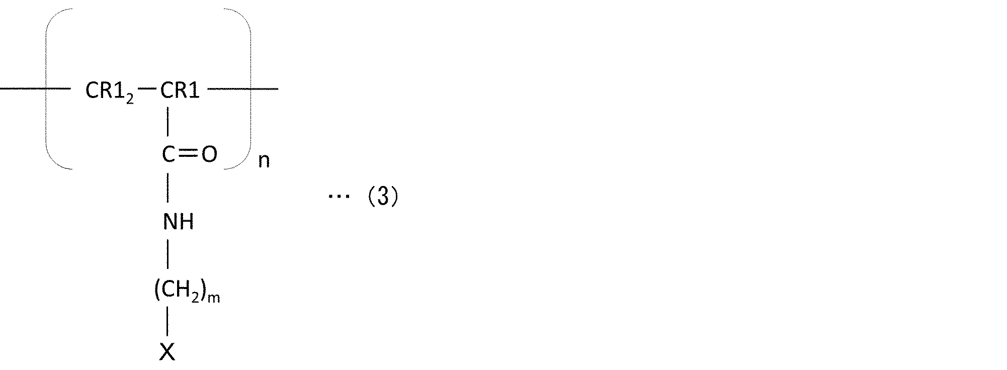
- the repeating unit contained in the ligand 18 may have a structure represented by the following chemical formula (3).
- m is a natural number.
- the numerical value of m affects the polarity of the precursor before polymerizing the ligands 18 including the repeating unit having the structure represented by the chemical formula (3).
- m is relatively small, for example, 1 or more and 5 or less, the precursor is easily dissolved in the aqueous solvent.
- m is relatively large, for example, 5 or more, the precursor is easily dissolved in the organic solvent. From the viewpoint of maintaining the efficiency of electron injection into the quantum dots 16 coordinated by the ligand 18, m is preferably 20 or less.
- repeating unit contained in the ligand 18 may have a structure represented by the following chemical formula (4).
- n1 and n2 are natural numbers. In the present embodiment, it is preferable that n1 is 1 or more and 3 or less and n2 is 1 or more and 10 or less. Further, in the present embodiment, each R3 is selected from a hydrogen atom, an alkyl group, an aryl group, an alkoxy group, or an amino group. Each R3 may be different or the same in the same repeating unit or in different repeating units. In the present embodiment, the ligand 18 includes a repeating unit having no side chain, which makes it possible to control the number of the modified functional groups 20 coordinated to one quantum dot 16.
- the hole transport layer 6 is a layer that transports holes from the anode 4 to the light emitting layer 8.
- the hole transport layer 6 may have a function of blocking electrons transported from the light emitting layer 8 toward the anode 4.
- the electron transport layer 10 is a layer that transports electrons from the cathode 12 to the light emitting layer 8.
- the electron transport layer 10 may have a function of inhibiting the transport of holes.
- Each of the hole transport layer 6 and the electron transport layer 10 may include a conventionally known material used for each transport layer, and may be formed by a sputtering method or the like.
- the thickness of each of the hole transport layer 6 and the electron transport layer 10 may be a conventionally known thickness, and may be, for example, 10 to 100 nm.
- an array substrate 3 including a TFT and various wirings connected to the TFT is manufactured, and an anode 4 electrically connected to the TFT is formed on the array substrate 3 by using a sputtering method or the like.
- the hole transport layer 6 is formed on the anode 4 by coating or the like.
- FIG. 3 is a flowchart for explaining the method of forming the light emitting layer 8.
- FIG. 4 is a diagram for explaining in detail each material synthesized in the step of forming the light emitting layer 8.
- each of the first ligands 22 has a polymerizable functional group having the above-described modified functional group 20 (first modified functional group) at the end of at least one side chain. Including.
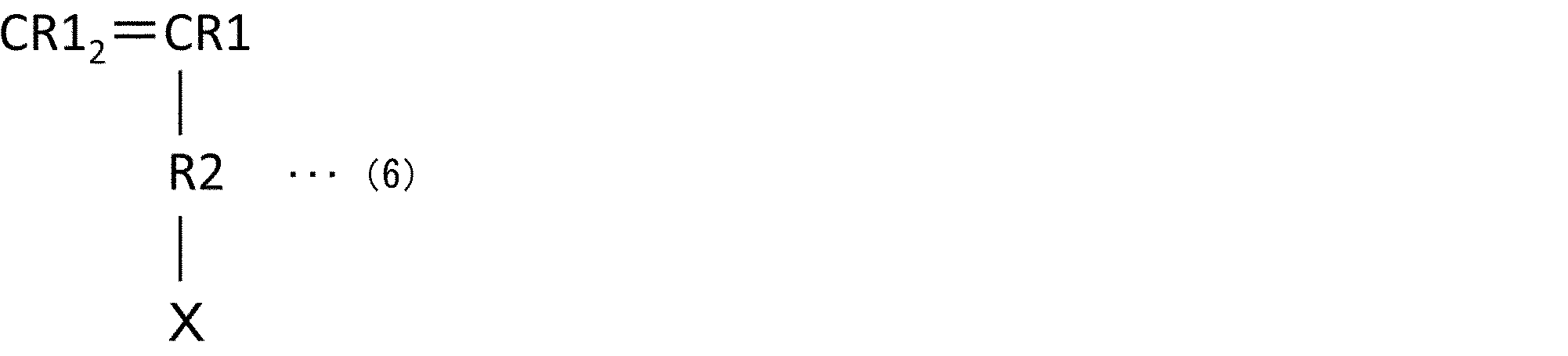
- the first ligand 22 has, for example, a structure represented by the following chemical formula (5) or the following chemical formula (6).
- the first solution 24 may be, for example, an aqueous solvent or a non-aqueous solvent.
- the second ligand 26 shown in FIG. 4B is synthesized (step S6).
- Each of the second ligands 26 has a second modified functional group 28 at the end.
- the second ligand 26 may have a structure having a conventionally known modified functional group at the terminal of a linear alkyl such as alkylamine.
- a conventionally known ligand used as a ligand of a conventional quantum dot may be adopted as the second ligand 26.
- step S8 Separately from step S6, the quantum dots 16 described above are synthesized (step S8).
- a conventionally known synthesizing method can be adopted for synthesizing the quantum dots 16.
- Step S10 is performed by dispersing the quantum dots 16 and the second ligand 26 in the second solution 30 shown in FIG. 4B.
- the first solution 24 is an aqueous solvent
- the second solution 30 is preferably an organic solvent
- the first solution 24 is a non-aqueous solvent
- the second solution 30 is an aqueous solvent. It is preferable.
- step S12 a substitution step of substituting the second ligand 26 for the ligand coordinated to the quantum dot 16 with the first ligand 22 is performed (step S12).
- the replacement step will be described in more detail with reference to FIG. 5A to 5C are process diagrams for explaining the replacement process.
- the first solution 24 and the second solution 30 are injected into the stirring container 32.
- the first solution 24 containing an excess amount of the first ligand 22 than the first ligand 22 actually coordinated to the quantum dots 16 is injected into the stirring container 32 after the substitution process. It is preferable.
- 1 ml of water containing 300 mg/ml of the first ligand 22 is injected as the first solution 24 into the stirring container 32.
- 100 ⁇ l of hexane containing 24 mg/ml of the quantum dots 16 and the alkylamine that is the second ligand 26 is injected as the second solution 30 into the stirring container 32.
- the stirring container 32 is sealed, and the stirring process is performed overnight to stir the first solution 24 and the second solution 30.
- the first solution 24 contains an excessive amount of the first ligand 22, the ligand coordinated to the quantum dot 16 gradually replaces the second ligand 26 with the first ligand 22 during the above stirring.
- the first solution 24 including the quantum dots 16 and the first ligand 22 coordinated with the quantum dots 16 is obtained.
- the second ligand 26 remains in the second solution 30.
- the extracted first solution 24 may be placed in a centrifuge tube and centrifuged.
- the centrifugation may be performed, for example, at a rotation speed of 4000 rpm for 10 minutes.
- the quantum dots 16 that are not dispersed in the first solution 24 can be removed.
- the mass ratio between the quantum dots 16 and the first ligand 22 in the first solution 24 is preferably 10:90 to 1:99.
- the first solution 24 extracted by the method described above is applied onto the hole transport layer 6 on which film formation has been completed (step S14).
- the polymerizable functional group in the first solution 24 is polymerized by irradiating ultraviolet rays having a wavelength of 365 nm.
- step S26 the polymerizable functional group of the first ligand 22 can be polymerized while removing the solvent of the first solution 24.
- the light emitting layer 8 including the quantum dots 16 to which the ligands 18 described above are coordinated is formed. With the above, the formation process of the light emitting layer 8 in the present embodiment is completed.
- the first ligand 22 may include, for example, acrylamide represented by the following chemical formula (7).
- the above-mentioned polymerization step is performed to obtain the light emitting layer 8 including the ligand 18 containing the structure represented by the following chemical formula (8) as a repeating unit.
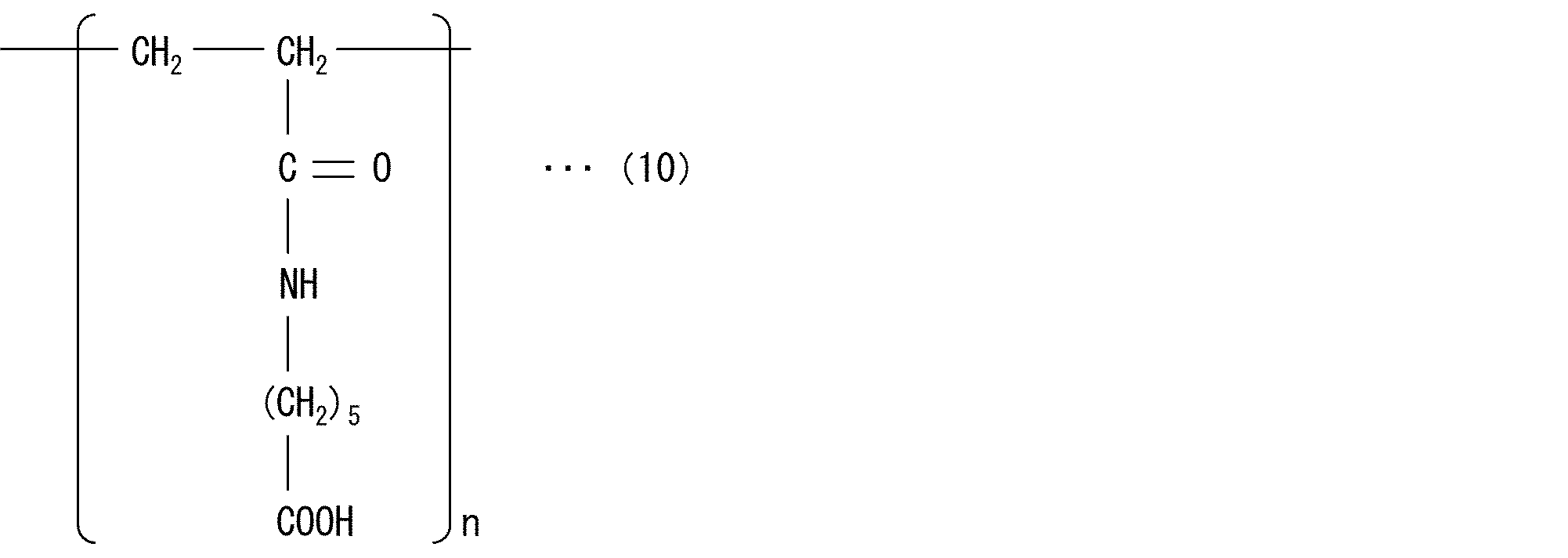
- the first ligand 22 may include, for example, 6-acrylamidohexanoic acid represented by the following chemical formula (9).
- the light emitting layer 8 including the ligand 18 containing a structure represented by the following chemical formula (10) as a repeating unit is shown. Is obtained.
- the first ligand 22 may include an acroyl group such as acrylamide and 6-acrylamidohexanoic acid described above.
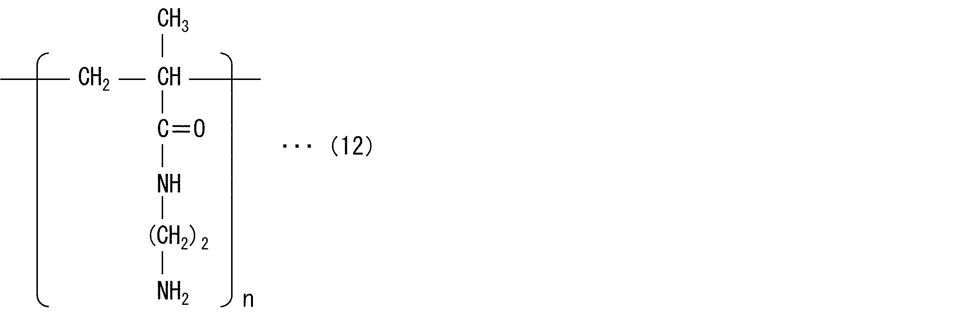
- the first ligand 22 may include a metaacryloyl group such as 2-aminoethylmethacrylamide shown in the following chemical formula (11).
- the above-mentioned polymerization step is carried out to provide a light emitting layer provided with a ligand 18 containing a structure represented by the following chemical formula (12) as a repeating unit. 8 is obtained.
- the first solution 24 may include an unsubstituted or substituted alkene as represented by the following chemical formula (13).
- an unsubstituted or substituted alkene and the first ligand 22 having a polymerizable functional group represented by the chemical formula (6) may be copolymerized.
- the quantum dot 16 in which the ligand 18 containing the structure represented by the chemical formula (4) as a repeating unit coordinates is obtained by the polymerization step.
- the polymerizable functional groups of the first ligand 22 in the first solution 24 may be polymerized, and all of the polymerizable functional groups of the first ligand 22 may be polymerized. Need not be polymerized. That is, a part of the polymerizable functional group before the polymerization may remain in the light emitting layer 8 in the present embodiment, and the light emitting layer 8 may include the ligand 18 having the polymerizable functional group.
- the electron transport layer 10 is formed on the upper layer of the light emitting layer 8 by coating or the like, and the cathode 12 is formed on the upper layer of the electron transport layer 10 by the sputtering method or the like to obtain the light emitting element 2 shown in FIG. .. Thereby, the light emitting device 1 according to the present embodiment is obtained.
- the method for manufacturing the light emitting layer 8 in the present embodiment includes a step of newly synthesizing each of the quantum dots 16, the first ligand 22, and the second ligand 26, but is not limited to this. ..
- the second solution 30 including a plurality of quantum dots 16 coordinated to the second ligand 26 only the first ligand 22 is synthesized and the above-mentioned substitution step is performed to thereby obtain the first ligand. It is possible to obtain the quantum dot 16 in which 22 is coordinated. That is, since the ligand coordinated to the quantum dot synthesized by the conventional technique can be replaced with the above-mentioned first ligand 22, the manufacturing process can be simplified.
- the first ligand 22 and the quantum dot 16 are separately synthesized, the ligand coordinated to the quantum dot 16 is replaced, and the quantum coordinated by the first ligand 22. It is possible to combine the dots 16. Therefore, even if the respective materials of the first ligand 22 and the quantum dots 16 are combinations that make it difficult to directly synthesize the quantum dots 16 coordinated by the first ligand 22, they are adopted in the present embodiment. be able to.
- the present embodiment is not limited to this, and for example, when the quantum dots 16 coordinated by the first ligand 22 can be directly synthesized, it is not necessary to synthesize the second ligand 26 and the replacement step can be omitted. Good.
- the light emitting layer 8 in the present embodiment has a structure in which the ligands 18 coordinated with the plurality of quantum dots 16 are polymerized with each other.
- the light emitting layer 8 is solidified so that the surface of the quantum dots 16 is covered with the polymerized ligand 18 by polymerizing the ligand 18. Therefore, even when the light emitting layer 8 is formed, it is possible to form the light emitting layer 8 while appropriately controlling the distance between the quantum dots 16 without agglomeration of the plurality of quantum dots 16 with each other. Therefore, the stability of the quantum dots 16 in the light emitting layer 8 can be improved, and the device life of the light emitting device 2 is improved.
- each quantum dot 16 is covered with the polymerized ligand 18, the formation process of the light emitting layer 8 can be performed while physically protecting the quantum dot 16. Therefore, even after the light emitting layer 8 is formed, the state in which the ligand 18 is stably coordinated with the quantum dot 16 can be maintained. Further, the polymerized ligand 18 around the quantum dots 16 can protect the quantum dots 16 from deterioration caused by oxygen or moisture. Therefore, the stability of the quantum dots 16 in the light emitting layer 8 can be further improved, and the device life of the light emitting device 2 is further improved.
- a binder may be added to a solution containing quantum dots in order to improve the dispersibility of the quantum dots in the solution, but the inclusion of the binder in the light emitting layer increases the resistance of the light emitting element. May be invited.
- the binder added to the first solution 24 can be reduced or removed.
- the ligand 18 since the ligand 18 has the modified functional group 20, it is easy to inject electrons from the outside to the inside of the quantum dot 16 as in the quantum dot in the conventional technique. Therefore, in the present embodiment, it is possible to reduce the increase in the resistance of the entire device while maintaining the efficiency of electron injection into the quantum dots.
- the polymerizable functional group of the first ligand 22 is formed. Polymerize. Therefore, it is not necessary to consider the compatibility between the modified functional group and the polymerizable functional group, so that the degree of freedom in selecting the material of the ligand 18 is improved.
Landscapes
- Chemical & Material Sciences (AREA)
- Engineering & Computer Science (AREA)
- Crystallography & Structural Chemistry (AREA)
- Inorganic Chemistry (AREA)
- Nanotechnology (AREA)
- Physics & Mathematics (AREA)
- Optics & Photonics (AREA)
- Materials Engineering (AREA)
- Electroluminescent Light Sources (AREA)
- Luminescent Compositions (AREA)
- Led Device Packages (AREA)
Abstract
本発明における発光素子は、アノードと、カソードと、前記アノードと前記カソードとの間の発光層とを含む発光素子であって、前記発光層は、複数の量子ドット(16)と、リガンド(18)とを含む。前記リガンドは、繰り返し単位を少なくとも2つ以上含む重合体であり、前記繰り返し単位のそれぞれは、前記複数の量子ドットの何れか1つに配位する修飾官能基(20)を、少なくとも1つの側鎖(18S)のそれぞれの末端に備える。
Description
本発明は量子ドットを含む発光素子、および当該発光素子を備えた発光デバイスに関する。
特許文献1は、量子ドットと、当該量子ドットの表面を覆う表面修飾部とを有するナノ粒子蛍光体を備えた発光装置を開示している。特許文献1に記載されているように、量子ドットの周囲に、当該量子ドットと配位結合する官能基を有したリガンドを配位させることにより、上述の量子ドットの溶媒中の安定性が向上する。
特許文献1に記載されているような、従来のリガンドでは、溶媒中の量子ドットの安定性を向上させることができるものの、当該量子ドットを積層し、成膜する工程において、量子ドットの安定性が低下する場合がある。このため、量子ドットを積層して備える層において、当該量子ドットが凝集し、劣化する虞がある。
上記の課題を解決するために、本発明の一態様に係る発光素子は、アノードと、カソードと、前記アノードと前記カソードとの間の発光層とを含む発光素子であって、前記発光層は、複数の量子ドットと、リガンドとを含み、前記リガンドは、繰り返し単位を少なくとも2つ以上含む重合体であり、前記繰り返し単位のそれぞれは、前記複数の量子ドットの何れか1つに配位する修飾官能基を、少なくとも1つの側鎖のそれぞれの末端に備える。
また、上記の課題を解決するために、本発明の一態様に係る発光素子の製造方法は、複数の量子ドットと、当該複数の量子ドットの何れか1つに配位する第1修飾官能基を、少なくとも1つの側鎖の末端に有する重合性官能基をそれぞれ含む、複数の第1リガンドとを備えた第1溶液を加熱しつつ、該第1溶液に紫外線を照射して、前記複数の量子ドットと、前記重合性官能基の少なくとも一部が互いに重合した前記第1リガンドとを備えた発光層を成膜する重合工程を備える。
本発明の一態様によれば、量子ドットを含む層における、当該量子ドットの安定性を改善できる。
〔実施形態1〕
図2は、本実施形態に係る発光デバイス1の概略断面図である。
図2は、本実施形態に係る発光デバイス1の概略断面図である。
図2に示すように、本実施形態に係る発光デバイス1は、発光素子2とアレイ基板3とを備える。発光デバイス1は、図示しないTFT(Thin Film Transistor)が形成されたアレイ基板3上に、発光素子2の各層が積層された構造を備える。なお、本明細書においては、発光デバイス1の発光素子2からアレイ基板3への方向を「下方向」、発光素子2のアレイ基板3から発光素子2への方向を「上方向」として記載する。
発光素子2は、アノード4上に、正孔輸送層6と、発光層8と、電子輸送層10と、カソード12とを、下層からこの順に備える。アレイ基板3の上層に形成された発光素子2のアノード4は、アレイ基板3のTFTと電気的に接続されている。他の実施形態に係る発光素子においては、アレイ基板の上層にカソードを備え、カソード上に、電子輸送層と、発光層と、正孔輸送層と、アノードとを、この順に備える発光素子であってもよい。
アノード4およびカソード12は導電性材料を含み、それぞれ、正孔輸送層6および電子輸送層10と電気的に接続されている。
アノード4とカソード12との何れか一方は、透明電極である。透明電極としては、例えば、ITO、IZO、ZnO、AZO、またはBZO等が用いられ、スパッタ法等によって成膜されてもよい。また、アノード4またはカソード12のいずれか一方は金属材料を含んでいてもよく、金属材料としては、可視光の反射率の高いAl、Cu、Au、またはAg等が好ましい。
本実施形態において、発光層8は、複数の量子ドット(半導体ナノ粒子)16と、量子ドット16のそれぞれに配位するリガンド18とを含む。発光層8は、複数の発光層が積層したものであってもよい。ここで、発光層8における量子ドット16は、図2に示すように、規則正しく配置されている必要はなく、量子ドット16は無秩序に発光層8に含まれていてもよい。発光層8の膜厚は、5~50nmが好ましい。
発光層8が含む量子ドット16とリガンド18とを、図1を参照してより詳細に説明する。図1の(a)は、図2に示す領域Aについての拡大図であり、発光層8の量子ドット16とリガンド18とをより詳細に示す図である。図1の(b)は、図1の(a)に示す領域Bについての拡大図であり、発光層8の量子ドット16とリガンド18とをさらに詳細に示す図である。図1の(b)においては、図示と説明との簡単のため、図1の(a)と比較して、リガンド18の構造を簡略化して示す。
量子ドット16は、価電子帯準位と伝導帯準位とを有し、価電子帯準位の正孔と伝導帯準位の電子との再結合によって発光する発光材料であり、可視光の散乱がない単一の蛍光体粒子である。量子ドット16からの発光は、量子閉じ込め効果により狭いスペクトルを有するため、比較的深い色度の発光を得ることが可能である。
量子ドット16は、当該分野において利用される材料から適宜選択されてもよい。量子ドット16は、例えば、CdS、CdSe、CdTe、ZnS、ZnSe、ZnTe、InN、InP、InAs、InSb、AlP、AlS、AlAs、AlSb、GaN、GaP、GaAs、GaSb、PbS、PbSe、Si、Ge、MgS、MgSe、MgTe、およびこれらの組み合わせから成る群から選択される1または複数の半導体材料を含んでいてもよい。また、量子ドット16は、例えば、コアと、当該コアの外殻であるシェルとを有する、コア/シェル構造を備えていてもよい。
量子ドット16の粒径は3~15nm程度である。量子ドット16からの発光の波長は、量子ドット16の粒径によって制御することができる。このため、量子ドット16の粒径を制御することにより、発光デバイス1が発する光の波長を制御できる。
本実施形態において、リガンド18は、繰り返し単位を少なくとも2つ以上含む重合体である。リガンド18は、繰り返し単位同士が重合することにより形成された、少なくとも1つの主鎖18Mを備える。リガンド18は、全ての繰り返し単位同士が重合して形成された、単一の主鎖18Mを備えていてもよい。一方、リガンド18は、一部の繰り返し単位同士が重合して形成された主鎖18Mを複数備えていてもよい。
リガンド18が備える繰り返し単位のそれぞれは、少なくとも1つの側鎖18Sを有し、側鎖18Sのそれぞれの末端に、図1の各図に示す、修飾官能基20を備える。繰り返し単位同士が重合することにより、図1の(b)に示すように、主鎖18Mから延びる側鎖18Sのそれぞれの末端に、修飾官能基20を1つずつ備えた構造が形成される。
修飾官能基20のそれぞれは、複数の量子ドット16のうち、何れか1つの量子ドットに配位する。図1の(b)に示すように、同一の主鎖18Mから延びる複数の側鎖18Sが備える各修飾官能基20は、同一の量子ドット16に配位してもよく、互いに異なる量子ドット16に配位してもよい。また、図1の(b)に示すように、互いに異なる主鎖18Mからそれぞれ延びる側鎖18Sが備える各修飾官能基20が、同一の量子ドット16に配位していてもよい。修飾官能基20は、チオール基、ヒドロキシル基、カルボキシ基、およびアミノ基のうち、少なくとも1つを含むことが好ましい。
リガンド18が含む繰り返し単位は、ビニル基、ビニリデン基、またはビニレン基に由来する官能基を含んでいてもよい。すなわち、リガンド18が含む繰り返し単位は、例えば、下記化学式(1)または下記化学式(2)にて表される構造を有する。


他に、リガンド18が含む繰り返し単位は、下記化学式(3)にて表される構造を備えていてもよい。
他に、リガンド18が含む繰り返し単位は、下記化学式(4)にて表される構造を備えていてもよい。

正孔輸送層6は、アノード4からの正孔を発光層8へと輸送する層である。本実施形態においては、正孔輸送層6は、発光層8からアノード4へ向かって輸送される電子をブロックする機能を備えていてもよい。電子輸送層10は、カソード12からの電子を発光層8へと輸送する層である。電子輸送層10は、正孔の輸送を阻害する機能を有していてもよい。
正孔輸送層6と電子輸送層10とのそれぞれは、各輸送層に使用される従来公知の材料を含んでいてもよく、スパッタ法等によって成膜されてもよい。正孔輸送層6と電子輸送層10とのそれぞれの膜厚は、従来公知の膜厚を採用でき、例えば、10~100nmであってもよい。
次に、本実施形態に係る発光デバイス1の製造方法について説明する。
はじめに、TFTと当該TFTに接続する各種配線とを備えたアレイ基板3を作製し、TFTに電気的に接続するアノード4を、スパッタ法等を使用してアレイ基板3上に形成する。次いで、アノード4の上層に、正孔輸送層6を、塗布形成等によって形成する。
次いで、発光層8を形成する。ここで、図3および図4を参照し、発光層8の形成について詳細に説明する。図3は、発光層8の形成方法について説明するためのフローチャートである。図4は、発光層8の形成工程において合成される各材料を詳細に説明するための図である。
はじめに、図4の(a)に示す、複数の第1リガンド22を合成する(ステップS2)。図4の(a)に示すように、第1リガンド22のそれぞれは、少なくとも1つの側鎖の末端に、上述した修飾官能基20(第1修飾官能基)を備えた、重合性官能基を含む。
第1リガンド22は、例えば、下記化学式(5)または下記化学式(6)にて表される構造を有する。

ここで、ステップS2およびステップS4とは別に、図4の(b)に示す、第2リガンド26を合成する(ステップS6)。第2リガンド26のそれぞれは、末端に第2修飾官能基28を備える。第2リガンド26は、アルキルアミン等、直鎖アルキルの末端に、従来公知の修飾官能基を備えた構造を有していてもよい。他にも、従来の量子ドットのリガンドとして使用される、従来公知のリガンドを、第2リガンド26に採用してもよい。
また、ステップS6とは別に、上述した量子ドット16を合成する(ステップS8)。量子ドット16の合成には、従来公知の合成方法を採用できる。
ステップS6およびステップS8に次いで、量子ドット16と第2修飾官能基28とを配位結合させ、量子ドット16に、第2リガンド26を配位させる(ステップS10)。ステップS10は、量子ドット16と第2リガンド26とを、図4の(b)に示す、第2溶液30中に分散させることにより実施する。第1溶液24が水系溶媒である場合には、第2溶液30は有機系溶媒であることが好ましく、第1溶液24が非水系溶媒である場合には、第2溶液30は水系溶媒であることが好ましい。
次いで、量子ドット16に配位するリガンドを、第2リガンド26から第1リガンド22に置換する置換工程を実施する(ステップS12)。置換工程について、図5を参照してより詳細に説明する。図5の各図は、置換工程を説明するための工程図である。
置換工程においては、始めに、図5の(a)に示すように、撹拌容器32に、第1溶液24と第2溶液30とを注入する。ここでは、撹拌容器32には、置換工程後、実際に量子ドット16に配位する第1リガンド22よりも、過剰量の第1リガンド22を含む第1溶液24を、撹拌容器32に注入することが好ましい。例えば、撹拌容器32に、第1溶液24として、第1リガンド22を300mg/ml含む水を1ml注入する。また、例えば、撹拌容器32には、第2溶液30として、量子ドット16と、第2リガンド26であるアルキルアミンとを、24mg/ml含むヘキサンを100μl注入する。この際、撹拌容器32に撹拌子34を入れることが好ましい。
次いで、撹拌容器32を密封し、終夜撹拌処理を行うことにより、第1溶液24と第2溶液30との撹拌を行う。ここで、第1溶液24が過剰量の第1リガンド22を含むために、上述の撹拌の間、量子ドット16に配位するリガンドが、次第に第2リガンド26から第1リガンド22に置き換わる。これにより、図5の(b)に示すように、量子ドット16と、当該量子ドット16に配位する第1リガンド22とを含む、第1溶液24が得られる。なお、第2リガンド26は第2溶液30中に残存する。
なお、第1溶液24のみを撹拌容器32から抽出する方法としては、マイクロピペット等を使用して抽出する手法が挙げられる。ここで、上述したように、第1溶液24の溶媒と第2溶液30との溶媒の系が異なっていることにより、図5の各図に示すように、両溶液が撹拌容器32中において分離する。このため、上記構成により、量子ドット16と、当該量子ドット16に配位する第1リガンド22とを含む、第1溶液24のみを容易に抽出しやすくなる。
ここで、抽出した第1溶液24を遠沈管に入れ、遠心分離を行ってもよい。遠心分離は、例えば、4000rpmの回転速度にて、10分間行ってもよい。これにより、第1溶液24中において、分散していない量子ドット16を除去できる。この際、第1溶液24における量子ドット16と第1リガンド22との質量比は、10:90~1:99であることが好ましい。
次いで、上述した手法により抽出した第1溶液24を、成膜が完了した正孔輸送層6上に塗布する(ステップS14)。次いで、塗布された第1溶液24を、例えば、摂氏100度程度に加熱しつつ、波長が365nmの紫外線を照射することにより、第1溶液24中の重合性官能基を重合させる、重合工程を実施する(ステップS26)。これにより、第1溶液24の溶媒を除去しつつ、第1リガンド22の重合性官能基を重合させることができる。ステップS26により、上述したリガンド18が配位する量子ドット16を含む、発光層8が成膜される。以上により、本実施形態における発光層8の形成工程が完了する。
本実施形態における発光層の形成工程において、第1リガンド22は、例えば、下記化学式(7)に示す、アクリルアミドを含んでいてもよい。


他に、本実施形態における発光層の形成工程において、第1リガンド22は、例えば、下記化学式(11)に示す、2-アミノエチルメタクリルアミドのような、メタアクロイル基を含んでいてもよい。


なお、本実施形態における重合工程においては、少なくとも、第1溶液24中の一部の第1リガンド22の重合性官能基同士が重合すればよく、全ての第1リガンド22の重合性官能基同士を重合させる必要はない。すなわち、本実施形態における発光層8には、重合前の重合性官能基が一部残存していてもよく、発光層8が、重合性官能基を有するリガンド18を含んでいてもよい。
最後に、発光層8の上層に、塗布形成等により電子輸送層10を形成し、当該電子輸送層10の上層に、スパッタ法等によりカソード12を形成し、図2に示す発光素子2を得る。これにより、本実施形態に係る発光デバイス1が得られる。
なお、本実施形態における発光層8の製造方法は、量子ドット16と、第1リガンド22と、第2リガンド26とのそれぞれを、新たに合成する工程を備えているが、これに限られない。例えば、既に第2リガンド26に配位した量子ドット16を複数備えた第2溶液30がある場合には、第1リガンド22のみを合成し、上述した置換工程を実施することにより、第1リガンド22が配位する量子ドット16を得ることができる。すなわち、従来技術によって合成された量子ドットに配位するリガンドを、上述する第1リガンド22に置き換えることができるため、製造工程を簡略化できる。
また、本実施形態における発光層8の製造方法により、第1リガンド22と量子ドット16とを別々に合成し、量子ドット16に配位するリガンドを置き換えて、第1リガンド22が配位する量子ドット16を合成することが可能である。したがって、第1リガンド22および量子ドット16のそれぞれの材料が、第1リガンド22が配位する量子ドット16を直接合成することが困難となるような組み合わせであっても、本実施形態に採用することができる。しかしながら、本実施形態においてはこれに限られず、例えば、第1リガンド22が配位する量子ドット16を直接合成できる場合には、第2リガンド26を合成する必要はなく、置換工程も省略してよい。
本実施形態における発光層8は、複数の量子ドット16にそれぞれ配位するリガンド18同士が、互いに重合している構造を備える。発光層8の形成工程において、リガンド18が高分子化することにより、量子ドット16の表面が高分子化したリガンド18によって覆われるように、発光層8が固化する。このため、発光層8の形成時においても、複数の量子ドット16が互いに凝集することなく、量子ドット16同士の距離を適切に制御しつつ、発光層8を形成することができる。ゆえに、発光層8中における量子ドット16の安定性を向上させることができ、発光素子2の素子寿命が改善する。
また、個々の量子ドット16の周囲を、高分子化したリガンド18によって覆うため、物理的に量子ドット16を保護しつつ、発光層8の形成工程を実施できる。このため、発光層8の形成後においても、リガンド18が安定して量子ドット16に配位した状態を保持できる。さらに、量子ドット16の周囲の高分子化したリガンド18により、量子ドット16を、酸素または水分に起因する劣化から保護できる。ゆえに、発光層8中における量子ドット16の安定性をさらに向上させることができ、発光素子2の素子寿命がさらに改善する。
従来技術においては、溶液中における量子ドットの分散性を向上させるために、量子ドットを含む溶液にバインダーを添加する場合があるが、当該バインダーを発光層が含むことは、発光素子の抵抗の上昇を招来する可能性がある。本実施形態においては、リガンド18を高分子化させて、発光層8における量子ドット16の安定性を向上させるため、第1溶液24に添加するバインダーを低減、あるいは除去できる。本実施形態において、リガンド18は修飾官能基20を有するために、従来技術における量子ドットと同様に、量子ドット16の外部から内部への電子の注入は容易である。このため、本実施形態においては、量子ドットへの電子注入の効率を維持しつつ、素子全体の抵抗が増加することを低減できる。
さらに、従来技術においては、量子ドットを含む溶液に、バインダーを添加する場合、当該バインダーと、量子ドットに配位するリガンドとの相性を考慮する必要がある。本実施形態においては、配位性を有する修飾官能基と、重合性官能基とを、両方備えた第1リガンド22を量子ドット16に配位させた後、第1リガンド22の重合性官能基を重合させる。このために、修飾官能基と重合性官能基との相性を考慮する必要がないため、リガンド18の材料の選択自由度が向上する。
本発明は上述した各実施形態に限定されるものではなく、請求項に示した範囲で種々の変更が可能であり、異なる実施形態にそれぞれ開示された技術的手段を適宜組み合わせて得られる実施形態についても本発明の技術的範囲に含まれる。さらに、各実施形態にそれぞれ開示された技術的手段を組み合わせることにより、新しい技術的特徴を形成することができる。
1 発光デバイス
2 発光素子
3 アレイ基板
4 アノード
6 正孔輸送層
8 発光層
10 電子輸送層
12 カソード
16 量子ドット
18 リガンド
18M 主鎖
18S 側鎖
20 (第1)修飾官能基
22 第1リガンド
24 第1溶液
26 第2リガンド
28 第2修飾官能基
30 第2溶液
2 発光素子
3 アレイ基板
4 アノード
6 正孔輸送層
8 発光層
10 電子輸送層
12 カソード
16 量子ドット
18 リガンド
18M 主鎖
18S 側鎖
20 (第1)修飾官能基
22 第1リガンド
24 第1溶液
26 第2リガンド
28 第2修飾官能基
30 第2溶液
Claims (20)
- アノードと、カソードと、前記アノードと前記カソードとの間の発光層とを含む発光素子であって、
前記発光層は、複数の量子ドットと、リガンドとを含み、
前記リガンドは、繰り返し単位を少なくとも2つ以上含む重合体であり、
前記繰り返し単位のそれぞれは、前記複数の量子ドットの何れか1つに配位する修飾官能基を、少なくとも1つの側鎖のそれぞれの末端に備えた発光素子。 - 前記リガンドが、ビニル基、ビニリデン基、またはビニレン基に由来する前記繰り返し単位を含む請求項1に記載の発光素子。
- 前記リガンドが、アクロイル基、またはメタアクロイル基に由来する前記繰り返し単位を含む請求項2に記載の発光素子。
- 前記リガンドが、下記化学式(1)または下記化学式(2)にて表される前記繰り返し単位を含み、


nは自然数であり、
Xは前記修飾官能基であり、
R1のそれぞれは、水素原子、アルキル基、アリール基、またはアルコキシ基から選択され、
R2は、置換もしくは無置換のアルカンジイル基、置換もしくは無置換のアルケンジイル基、ペプチド結合、エステル結合、カルボニル基、およびイミノ基のうち、少なくとも1種を含む請求項1から3の何れか1項に記載の発光素子。 - 前記リガンドが、下記化学式(3)にて表される前記繰り返し単位を含み、
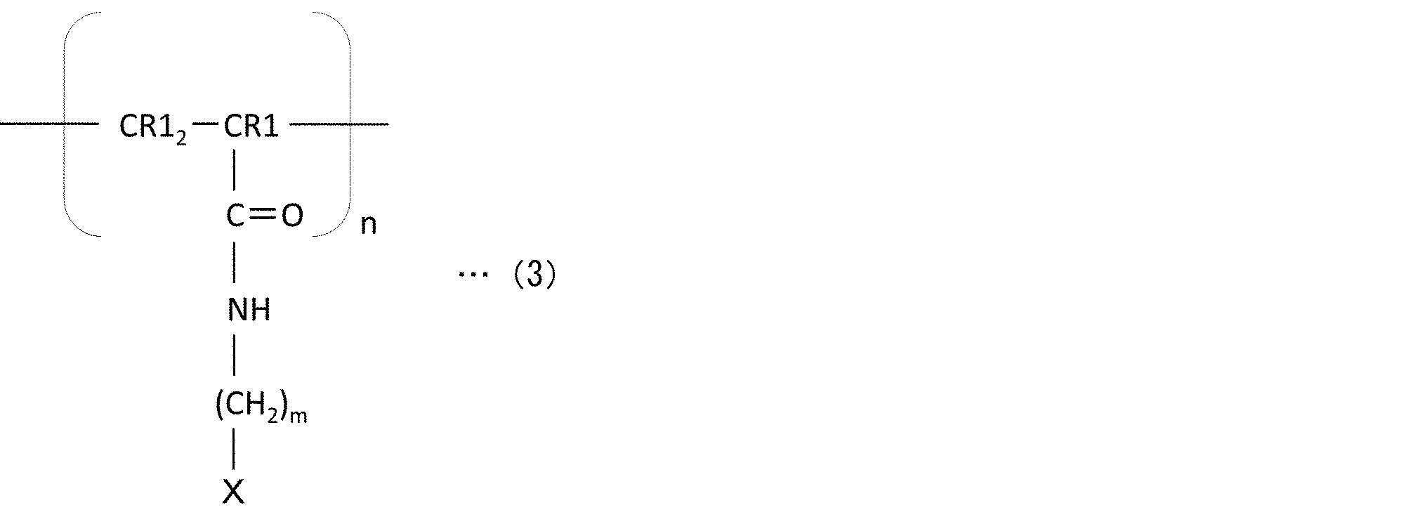
nおよびmはそれぞれ自然数であり、
Xは前記修飾官能基であり、
R1のそれぞれは、水素原子、アルキル基、アリール基、またはアルコキシ基から選択される請求項1から3の何れか1項に記載の発光素子。 - mが1以上5以下である請求項5に記載の発光素子。
- mが5以上20以下である請求項5に記載の発光素子。
- 前記リガンドが、下記化学式(4)にて表される前記繰り返し単位を含み、
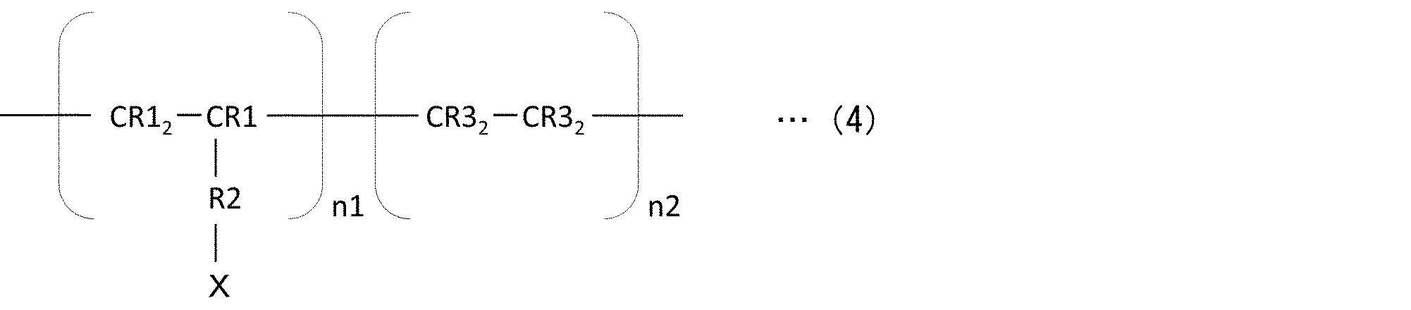
n1およびn2はそれぞれ自然数であり、
Xは前記修飾官能基であり、
R1のそれぞれは、水素原子、アルキル基、アリール基、またはアルコキシ基から選択され、
R2は、置換もしくは無置換のアルカンジイル基、置換もしくは無置換のアルケンジイル基、ペプチド結合、エステル結合、カルボニル基、およびイミノ基のうち、少なくとも1種を含み、
R3のそれぞれは、水素原子、アルキル基、アリール基、アルコキシ基、またはアミノ基から選択される請求項1から3の何れか1項に記載の発光素子。 - n1が1以上3以下であり、n2が1以上10以下である請求項8に記載の発光素子。
- 前記リガンドが重合性官能基を含む請求項1から9の何れか1項に記載の発光素子。
- 前記修飾官能基が、チオール基、ヒドロキシル基、カルボキシ基、およびアミノ基のうち、少なくとも1つを含む請求項1から10の何れか1項に記載の発光素子。
- 前記アノードと前記発光層との間に正孔輸送層を備え、前記カソードと前記発光層との間に電子輸送層を備えた請求項1から11の何れか1項に記載の発光素子。
- 請求項1から12の何れか1項に記載の発光素子を備えた発光デバイス。
- 複数の量子ドットと、当該複数の量子ドットの何れか1つに配位する第1修飾官能基を、少なくとも1つの側鎖の末端に有する重合性官能基をそれぞれ含む、複数の第1リガンドとを備えた第1溶液を加熱しつつ、該第1溶液に紫外線を照射して、前記複数の量子ドットと、前記重合性官能基の少なくとも一部が互いに重合した前記第1リガンドとを備えた発光層を成膜する重合工程を備えた発光素子の製造方法。
- 前記重合工程の前における前記第1リガンドが、下記化学式(5)または下記化学式(6)にて表され、

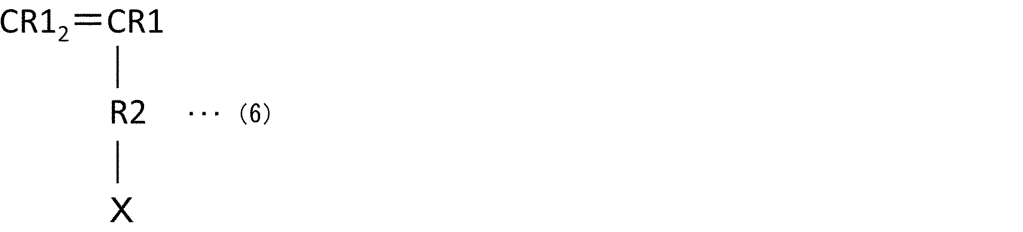
nは自然数であり、
Xは前記第1修飾官能基であり、
R1のそれぞれは、水素原子、アルキル基、アリール基、またはアルコキシ基から選択され、
R2は、置換もしくは無置換のアルカンジイル基、置換もしくは無置換のアルケンジイル基、エステル結合、カルボニル基、およびイミノ基のうち、少なくとも1種を含む請求項14に記載の発光素子の製造方法。 - 前記重合工程の前における前記第1リガンドが、6-アクリルアミドヘキサン酸または2-アミノエチルメタクリルアミドを含む請求項14に記載の発光素子の製造方法。
- 前記第1修飾官能基が、チオール基、ヒドロキシル基、カルボキシ基、およびアミノ基うち、少なくとも1つを含む請求項14から16の何れか1項に記載の発光素子の製造方法。
- 前記重合工程に先立って、前記第1リガンドを含む第1溶液と、前記複数の量子ドットと、当該複数の量子ドットのうち少なくとも1つの量子ドットに配位する第2修飾官能基を有し、重合性官能基を有さない第2リガンドとを備えた第2溶液とを撹拌し、前記複数の量子ドットに配位するリガンドを、前記第2リガンドから前記第1リガンドに置き換える置換工程をさらに備えた請求項14から17の何れか1項に記載の発光素子の製造方法。
- 前記第1溶液の溶媒が水系溶媒であり、前記第2溶液の溶媒が有機系溶媒である請求項18に記載の発光素子の製造方法。
- 前記第1溶液の溶媒が非水系溶媒であり、前記第2溶液の溶媒が水系溶媒である請求項18に記載の発光素子の製造方法。
Priority Applications (3)
| Application Number | Priority Date | Filing Date | Title |
|---|---|---|---|
| PCT/JP2019/000967 WO2020148812A1 (ja) | 2019-01-15 | 2019-01-15 | 発光素子、発光デバイス、発光素子の製造方法 |
| US17/421,370 US20220059766A1 (en) | 2019-01-15 | 2019-01-15 | Light-emitting element, light-emitting device, and method of manufacturing light-emitting element |
| CN201980087172.8A CN113272973A (zh) | 2019-01-15 | 2019-01-15 | 发光元件、发光装置、发光元件的制造方法 |
Applications Claiming Priority (1)
| Application Number | Priority Date | Filing Date | Title |
|---|---|---|---|
| PCT/JP2019/000967 WO2020148812A1 (ja) | 2019-01-15 | 2019-01-15 | 発光素子、発光デバイス、発光素子の製造方法 |
Publications (1)
| Publication Number | Publication Date |
|---|---|
| WO2020148812A1 true WO2020148812A1 (ja) | 2020-07-23 |
Family
ID=71613280
Family Applications (1)
| Application Number | Title | Priority Date | Filing Date |
|---|---|---|---|
| PCT/JP2019/000967 Ceased WO2020148812A1 (ja) | 2019-01-15 | 2019-01-15 | 発光素子、発光デバイス、発光素子の製造方法 |
Country Status (3)
| Country | Link |
|---|---|
| US (1) | US20220059766A1 (ja) |
| CN (1) | CN113272973A (ja) |
| WO (1) | WO2020148812A1 (ja) |
Families Citing this family (1)
| Publication number | Priority date | Publication date | Assignee | Title |
|---|---|---|---|---|
| CN114058269B (zh) * | 2021-11-29 | 2023-09-01 | 镭昱光电科技(苏州)有限公司 | 量子点光固化胶水及其制备方法、显示装置 |
Citations (5)
| Publication number | Priority date | Publication date | Assignee | Title |
|---|---|---|---|---|
| JP2010114079A (ja) * | 2008-11-05 | 2010-05-20 | Samsung Electronics Co Ltd | 量子ドット発光素子およびその製造方法 |
| WO2014091855A1 (ja) * | 2012-12-10 | 2014-06-19 | シャープ株式会社 | 樹脂組成物および該樹脂組成物を波長変換部に用いた発光装置 |
| JP2015220069A (ja) * | 2014-05-16 | 2015-12-07 | 株式会社ジャパンディスプレイ | 表示装置 |
| US20150380653A1 (en) * | 2014-06-25 | 2015-12-31 | Boe Technology Group Co., Ltd. | Electro-Luminescence Display Panel and Fabrication Method Thereof, Display Device |
| JP2017524156A (ja) * | 2014-07-22 | 2017-08-24 | コーニンクレッカ フィリップス エヌ ヴェKoninklijke Philips N.V. | 赤色照明のカラーコンバータを得るための、シリコーンホスト中で量子ドットを分散させるために使用されるシロキサン配位子 |
Family Cites Families (10)
| Publication number | Priority date | Publication date | Assignee | Title |
|---|---|---|---|---|
| CA2506388A1 (en) * | 2004-05-05 | 2005-11-05 | Tieneke Emily Dykstra | Surface modification of nanocrystals using multidentate polymer ligands |
| US20080237611A1 (en) * | 2007-03-29 | 2008-10-02 | Cok Ronald S | Electroluminescent device having improved contrast |
| US10035952B2 (en) * | 2012-10-25 | 2018-07-31 | Lumileds Llc | PDMS-based ligands for quantum dots in silicones |
| JP6448782B2 (ja) * | 2015-05-28 | 2019-01-09 | 富士フイルム株式会社 | 量子ドット含有組成物、波長変換部材、バックライトユニット、および液晶表示装置 |
| CN106032468B (zh) * | 2015-12-31 | 2017-11-21 | 苏州星烁纳米科技有限公司 | 可聚合的量子点及其应用 |
| CN108242482B (zh) * | 2016-12-23 | 2020-03-31 | 苏州星烁纳米科技有限公司 | 量子点发光层的制备及含该发光层的电致发光器件 |
| CN107134533B (zh) * | 2017-05-12 | 2019-05-03 | 苏州星烁纳米科技有限公司 | 电致发光器件、显示装置及照明装置 |
| CN108129661B (zh) * | 2018-01-03 | 2021-01-22 | 京东方科技集团股份有限公司 | 一种聚合物、量子点膜层及其制备方法 |
| CN108441221B (zh) * | 2018-05-10 | 2021-06-01 | 河北工业大学 | 一种与封装硅胶高兼容核壳量子点材料及其制备方法 |
| CN109180853B (zh) * | 2018-07-19 | 2021-01-15 | 京东方科技集团股份有限公司 | Tadf聚合物配体、量子点材料和其制备方法及应用 |
-
2019
- 2019-01-15 WO PCT/JP2019/000967 patent/WO2020148812A1/ja not_active Ceased
- 2019-01-15 US US17/421,370 patent/US20220059766A1/en active Pending
- 2019-01-15 CN CN201980087172.8A patent/CN113272973A/zh active Pending
Patent Citations (5)
| Publication number | Priority date | Publication date | Assignee | Title |
|---|---|---|---|---|
| JP2010114079A (ja) * | 2008-11-05 | 2010-05-20 | Samsung Electronics Co Ltd | 量子ドット発光素子およびその製造方法 |
| WO2014091855A1 (ja) * | 2012-12-10 | 2014-06-19 | シャープ株式会社 | 樹脂組成物および該樹脂組成物を波長変換部に用いた発光装置 |
| JP2015220069A (ja) * | 2014-05-16 | 2015-12-07 | 株式会社ジャパンディスプレイ | 表示装置 |
| US20150380653A1 (en) * | 2014-06-25 | 2015-12-31 | Boe Technology Group Co., Ltd. | Electro-Luminescence Display Panel and Fabrication Method Thereof, Display Device |
| JP2017524156A (ja) * | 2014-07-22 | 2017-08-24 | コーニンクレッカ フィリップス エヌ ヴェKoninklijke Philips N.V. | 赤色照明のカラーコンバータを得るための、シリコーンホスト中で量子ドットを分散させるために使用されるシロキサン配位子 |
Also Published As
| Publication number | Publication date |
|---|---|
| US20220059766A1 (en) | 2022-02-24 |
| CN113272973A (zh) | 2021-08-17 |
Similar Documents
| Publication | Publication Date | Title |
|---|---|---|
| KR102181060B1 (ko) | 금속 이온 표면 처리된 금속 산화물 나노입자, 이것을 포함하는 양자점-발광 소자 및 그 제조 방법 | |
| US10403690B2 (en) | Light emitting device including tandem structure with quantum dots and nanoparticles | |
| KR101794082B1 (ko) | 아민기를 갖는 덴드리머로 리간드 치환된 양자점 발광층을 포함하는 양자점 발광소자 및 이의 제조방법 | |
| KR102709934B1 (ko) | 비카드뮴 양자점 및 이를 포함한 복합체와 표시소자 | |
| KR101880596B1 (ko) | 양자점 또는 염료를 함유하는 대면적 필름 및 이의 제조 방법 | |
| KR102820492B1 (ko) | 양자점 및 이를 포함한 복합체와 표시소자 | |
| KR102715537B1 (ko) | 양자점, 양자점을 포함하는 조성물, 양자점 복합체, 표시 패널, 및 전자 장치 | |
| WO2007142203A1 (ja) | 量子ドット発光型無機el素子 | |
| KR102805261B1 (ko) | 전계 발광 소자 및 이를 포함하는 표시 장치 | |
| KR102886552B1 (ko) | 나노입자들를 포함하는 색변환패널, 나노입자, 및 이를 포함하는 전자소자 | |
| KR102814031B1 (ko) | 양자점, 복합체, 그리고 이를 포함하는 소자 | |
| WO2020174594A1 (ja) | 発光デバイス、表示デバイス | |
| US20220376196A1 (en) | Light-emitting device including mixtures of different quantum dots | |
| WO2020148812A1 (ja) | 発光素子、発光デバイス、発光素子の製造方法 | |
| US20230295491A1 (en) | Semiconductor nanoparticle, and color conversion panel and electronic device including the same | |
| US20240397743A1 (en) | Light-emitting element, ink, display device, and method for manufacturing light-emitting element | |
| WO2022190191A1 (ja) | 量子ドット含有膜、発光素子、波長変換部材、表示装置 | |
| KR102713258B1 (ko) | 비카드뮴 양자점 및 이를 포함한 복합체와 표시소자 | |
| JP7169207B2 (ja) | 量子ドット発光素子及び表示装置 | |
| EP4696761A1 (en) | Semiconductor nanoparticle, method of producing the same and electronic device including the same | |
| US20250241114A1 (en) | Electroluminescence device, production method thereof, and display device including the same | |
| EP4506434A1 (en) | Semiconductor nanoparticle, prodcution method thereof, electronic device including the same | |
| KR102870692B1 (ko) | 반도체 나노입자, 및 이를 포함하는 색변환패널과 전자소자 | |
| EP4596655A1 (en) | Semiconductor nanoparticle, method of producing the same and electronic device including the same | |
| US20250388807A1 (en) | Display device |
Legal Events
| Date | Code | Title | Description |
|---|---|---|---|
| 121 | Ep: the epo has been informed by wipo that ep was designated in this application |
Ref document number: 19910819 Country of ref document: EP Kind code of ref document: A1 |
|
| NENP | Non-entry into the national phase |
Ref country code: DE |
|
| 122 | Ep: pct application non-entry in european phase |
Ref document number: 19910819 Country of ref document: EP Kind code of ref document: A1 |
|
| NENP | Non-entry into the national phase |
Ref country code: JP |