WO2020144909A1 - 光コネクタおよびその製造方法 - Google Patents
光コネクタおよびその製造方法 Download PDFInfo
- Publication number
- WO2020144909A1 WO2020144909A1 PCT/JP2019/040819 JP2019040819W WO2020144909A1 WO 2020144909 A1 WO2020144909 A1 WO 2020144909A1 JP 2019040819 W JP2019040819 W JP 2019040819W WO 2020144909 A1 WO2020144909 A1 WO 2020144909A1
- Authority
- WO
- WIPO (PCT)
- Prior art keywords
- optical fiber
- ferrule
- face
- optical
- optical connector
- Prior art date
- Legal status (The legal status is an assumption and is not a legal conclusion. Google has not performed a legal analysis and makes no representation as to the accuracy of the status listed.)
- Ceased
Links
Images








Classifications
-
- G—PHYSICS
- G02—OPTICS
- G02B—OPTICAL ELEMENTS, SYSTEMS OR APPARATUS
- G02B6/00—Light guides; Structural details of arrangements comprising light guides and other optical elements, e.g. couplings
- G02B6/24—Coupling light guides
- G02B6/26—Optical coupling means
- G02B6/262—Optical details of coupling light into, or out of, or between fibre ends, e.g. special fibre end shapes or associated optical elements
-
- G—PHYSICS
- G02—OPTICS
- G02B—OPTICAL ELEMENTS, SYSTEMS OR APPARATUS
- G02B6/00—Light guides; Structural details of arrangements comprising light guides and other optical elements, e.g. couplings
- G02B6/24—Coupling light guides
- G02B6/36—Mechanical coupling means
- G02B6/38—Mechanical coupling means having fibre to fibre mating means
- G02B6/3807—Dismountable connectors, i.e. comprising plugs
- G02B6/3833—Details of mounting fibres in ferrules; Assembly methods; Manufacture
- G02B6/3847—Details of mounting fibres in ferrules; Assembly methods; Manufacture with means preventing fibre end damage, e.g. recessed fibre surfaces
-
- G—PHYSICS
- G02—OPTICS
- G02B—OPTICAL ELEMENTS, SYSTEMS OR APPARATUS
- G02B6/00—Light guides; Structural details of arrangements comprising light guides and other optical elements, e.g. couplings
- G02B6/24—Coupling light guides
- G02B6/36—Mechanical coupling means
- G02B6/38—Mechanical coupling means having fibre to fibre mating means
- G02B6/3807—Dismountable connectors, i.e. comprising plugs
- G02B6/381—Dismountable connectors, i.e. comprising plugs of the ferrule type, e.g. fibre ends embedded in ferrules, connecting a pair of fibres
- G02B6/3818—Dismountable connectors, i.e. comprising plugs of the ferrule type, e.g. fibre ends embedded in ferrules, connecting a pair of fibres of a low-reflection-loss type
-
- G—PHYSICS
- G02—OPTICS
- G02B—OPTICAL ELEMENTS, SYSTEMS OR APPARATUS
- G02B6/00—Light guides; Structural details of arrangements comprising light guides and other optical elements, e.g. couplings
- G02B6/24—Coupling light guides
- G02B6/36—Mechanical coupling means
- G02B6/38—Mechanical coupling means having fibre to fibre mating means
- G02B6/3807—Dismountable connectors, i.e. comprising plugs
- G02B6/381—Dismountable connectors, i.e. comprising plugs of the ferrule type, e.g. fibre ends embedded in ferrules, connecting a pair of fibres
- G02B6/3825—Dismountable connectors, i.e. comprising plugs of the ferrule type, e.g. fibre ends embedded in ferrules, connecting a pair of fibres with an intermediate part, e.g. adapter, receptacle, linking two plugs
Definitions
- the present invention relates to an optical connector for connecting a single mode optical fiber for visible light to ultraviolet light and a method for manufacturing the same.
- optical connectors such as SC type, FC type and LC type are used to connect a single mode optical fiber with a mode field diameter MFD of about 9 ⁇ m. ing.
- FC-type and LC-type connectors have come to be used even in the visible light region to the ultraviolet light region.
- the MFD of the single-mode optical fiber for visible light to ultraviolet light is as small as 2 ⁇ m to 4 ⁇ m, and even if the power is the same as the communication wavelength band, its power density is increased by one digit. Further, the energy of visible light to ultraviolet light is higher than the energy of light in the communication wavelength band, and the fiber end face is severely deteriorated (for example, see Patent Document 1).
- FIG. 1 shows an end surface after the optical connector that has passed through the light is removed and inserted. It is a case where light having a wavelength of 405 nm is transmitted for several hundred hours, (a) is an example when light is transmitted at 20 mW, and (b) is an example when light is transmitted at 60 mW. It can be seen that the core part near the center is deteriorated. Even if only light is passed for several hours, if the optical connector is removed and inserted, the transmission loss may increase to several tens of dB or more.
- the end face of the optical fiber including the ferrule of the optical connector and the core, is processed to be flush by polishing. Further, the optical fibers are polished to a slightly convex surface (PC polishing) so that the cores of the optical fibers facing each other physically contact each other.
- PC polishing slightly convex surface
- Figure 2 shows the structure of a conventional optical connector for connecting a single-mode optical fiber for visible light to ultraviolet light.
- Optical fibers 22a and 22b including single mode cores 21a and 21b are inserted into ferrules 23a and 23b, and coreless fibers (end caps) 24a and 24b are fusion-spliced to the end faces of the optical fibers 22a and 22b.
- Lenses 27a and 27b are incorporated in the sleeve 25, light 26a emitted from the end cap 24a is converted into collimated light 28 by the lens 27a, and light 26b condensed by the lens 27b is incident on the end cap 24b. To do.
- a coreless fiber with a length of about 300 ⁇ m was fused as an end cap on the end face and optically coupled via a lens.
- the power density of light at the connection end face is lowered, and the core end faces are prevented from physically contacting each other to prevent deterioration of the core end face.
- precision is required for the alignment of the optical axis of the lens and the optical axis of the optical fiber, and the structure is complicated and expensive.
- An object of the present invention is to provide an optical connector that can prevent deterioration of the end face of the core with a simple structure and a manufacturing method thereof.
- the present invention provides, in a first aspect, an optical connector for connecting a single mode optical fiber for visible light to ultraviolet light having a wavelength of 650 nm or less, wherein the optical fiber is
- the optical connector for connecting the optical fibers by inserting the fixed ferrule into a sleeve and abutting the sleeve, a film made of a nitride, an oxide or a fluoride is formed on the end faces of the optical fiber and the ferrule.
- At least one of the end faces of the optical fiber is at a position recessed from the end face of the ferrule, and when the ferrule is inserted into the sleeve, the end face is between the end faces of the optical fiber.
- the feature is that there is a gap.
- a third aspect is an optical connector for connecting a single-mode optical fiber for visible light having a wavelength of 650 nm or less to ultraviolet light, wherein a ferrule to which the optical fiber is fixed is inserted into a sleeve and abutted to each other.
- a ferrule to which the optical fiber is fixed is inserted into a sleeve and abutted to each other.
- the end face of the optical fiber and the end face of the ferrule are flush with each other, a spacer is inserted between the end faces of the ferrule, and a gap is formed between the end faces of the optical fiber. ..
- the protective film is formed on the end faces of the optical fibers and the end faces of the optical fibers do not contact each other, deterioration of the core end faces can be prevented.
- FIG. 3 is a diagram showing a method of forming a protective film of an optical connector according to Example 2.
- the figure which shows the structure of the optical connector for connecting the single mode optical fiber for visible light to ultraviolet light concerning Example 3 of 2nd Embodiment The figure which shows the structure which formed the non-reflective coating on the optical connector concerning Example 3.
- the figure which shows the structure of the optical connector for connecting the single mode optical fiber for visible light to ultraviolet light concerning Example 4 of 2nd Embodiment The figure which shows the structure of the optical connector for connecting the single mode optical fiber for visible light to ultraviolet light concerning Example 5 of 2nd Embodiment, The figure which shows the structure of the optical connector for connecting the single mode optical fiber for visible light to ultraviolet light concerning Example 6 of 2nd Embodiment, The figure which shows the 1st example of the method of denting an optical fiber end surface rather than the ferrule end surface, The figure which shows the 2nd example of the method of denting an optical fiber end surface rather than the ferrule end surface. The figure which shows the 3rd example of the method of denting an optical fiber end surface rather than the ferrule end surface. The figure which shows the result of the insertion/extraction test using the optical connector of this embodiment, It is a figure which shows the structure of the optical connector for connecting the single mode optical fiber for visible light to ultraviolet light concerning Example 5 of 3rd Embodiment.
- the cores of the optical fibers When visible light passes through the optical fiber, there is a phenomenon that the core swells. To prevent this, a protective film is formed. Further, by inserting/removing the optical connector, the cores of the optical fibers physically come into contact with each other or are separated from each other, whereby the deterioration of the end face of the core is promoted. Therefore, the optical fibers are not in physical contact with each other.
- the core end face is fixed at a position recessed from the end face of the ferrule by about 1 ⁇ m to 10 ⁇ m so that when the optical connector is connected, an air gap of 2 ⁇ m to 20 ⁇ m is formed between the core end faces. A gap of 2 ⁇ m to 5 ⁇ m is desirable. As a result, the end faces do not come into contact with each other and the end faces do not deteriorate. Alternatively, inserting a spacer between the ferrules avoids physical contact.
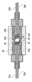
- FIG. 3 shows the structure of an optical connector for connecting a single mode optical fiber for visible light to ultraviolet light according to the first embodiment of the present invention.
- the optical fibers 22a and 22b including the single mode cores 21a and 21b are fixed to the ferrules 23a and 23b, and the ferrules 23a and 23b are inserted into the sleeve 25 and abutted.
- the optical fibers 22a and 22b are pure quartz core fibers for visible light to ultraviolet light having a wavelength of 650 nm or less.
- the end faces of the optical fibers 22a and 22b and the ferrules 23a and 23b are polished (angled PC (APC) polishing) at an inclination of 8 degrees with respect to the optical axis.
- the end faces of the optical fibers 22a and 22b are recessed from the end faces of the ferrules 23a and 23b by the method described later with reference to FIG. Specifically, the ferrule having the optical fiber fixed thereto is polished by angled PC, and then the end face is polished with a cerium oxide polishing liquid so that the end face of the optical fiber is recessed by about 2 ⁇ m from the end face of the ferrule.
- a gap G33 of about 5 ⁇ m is formed between the end faces. Since the end face has an angle of 8° with the optical axis, reflection is suppressed.
- the end faces do not come into contact with each other, and deterioration of the end faces can be suppressed.
- the end face of the core swells, resulting in a large transmission loss.
- a protective film of a nitride film, an oxide film, and a fluoride film is formed on the end face of the core at 0.5 ⁇ m to 3 ⁇ m. A thickness of 2 ⁇ m is desirable.
- an antireflection (AR) coat is further attached.
- the core end face is tilted by 90° ⁇ 1 to 10° instead of 90° with respect to the optical axis. hopefully 8 degrees is good.
- FIG. 4 shows the structure of an optical connector for connecting a single mode optical fiber for visible light to ultraviolet light according to Example 2 of the second embodiment.
- the optical fibers 22a and 22b including the single mode cores 21a and 21b are fixed to the ferrules 23a and 23b, and the ferrules 23a and 23b are inserted into the sleeve 25 and abutted.
- the optical fibers 22a and 22b are pure quartz core fibers for visible light to ultraviolet light having a wavelength of 650 nm or less.
- Si 3 N 4 films 31a and 31b having a thickness of 1.8 ⁇ m are formed as a protective film by sputtering.
- FIG. 5 shows a method of forming the protective film of the optical connector according to the second embodiment.
- the optical fiber 22 is inserted into the ferrule 23, and the optical fiber 22 is adhesively fixed to the ferrule 23 with an adhesive 28.
- the end faces of the optical fiber 22 and the ferrule 23 are vertically or obliquely polished, and the protective film 31 is formed by vapor deposition or sputtering.
- the polishing PC polishing, SPC polishing, or APC polishing can be applied.
- Example 3 In the structure shown in FIG. 4, the Si 3 N 4 films 31 are in physical contact with each other, and a mechanical force is applied when the optical connector is inserted and removed. As a result, the Si 3 N 4 film 31 deteriorates, so that the gap G33 is introduced as in the first embodiment.
- FIG. 6 shows the structure of an optical connector for connecting a single-mode optical fiber for visible light to ultraviolet light according to the third embodiment. Similar to the first embodiment, the end faces of the optical fibers 22a and 22b are recessed from the end faces of the ferrules 23a and 23b by the method described later with reference to FIG. In the third embodiment, when the ferrules 23a and 23b are inserted into the sleeve 25, a gap G33 of about 4 ⁇ m is formed between the end faces.
- FIG. 7 shows a configuration in which an antireflection coat is attached to the optical connector according to the third embodiment.
- an antireflection coat is attached to the optical connector according to the third embodiment.
- it is effective to form an antireflection coat and a protective film as shown in FIG.
- Si 3 N 4 films 31a, 31b, 34a to 34d having a thickness of 1.8 ⁇ m are formed by sputtering.
- anti-reflection coating SiO 2 films 32a, 32b, 35a to 35d having a thickness of 70 nm are formed on the end faces of the Si 3 N 4 films 31a, 31b, 34a to 34d by sputtering.
- a gap G33 of about 5 ⁇ m is formed between the end faces.
- the protective film 31 and the antireflection coat 32 are formed on the end face of the fiber, and the protective film 34 and the antireflection coat 35 are formed on the end face of the ferrule. The same, but with the former.
- the transmittance varies depending on the wavelength due to the interference of multiple reflection between the interface with the optical fiber and the interface on the gap side. Specifically, wavelength dependence appears between 95% and 80%. Further, when a pair of fiber blocks are connected so as to face each other, a cavity is formed, and the vibration is further increased to 50% to 98%. In order to prevent this, it is effective to form the SiO 2 films 32a and 32b on the Si 3 N 4 films 31a and 31b to a thickness of about 70 nm to form a non-reflection coating.
- the transmittance at one end is 95% to 100%, and the transmittance is 95% or more even if they are opposed to each other.
- An alumina (Al 2 O 3 ) film can be used instead of the Si 3 N 4 film, and SiO 2 (114 nm)/SiN (21.5 nm)/SiO 2 (86.5 nm) is formed on alumina 1.8 ⁇ m.
- the transmittance becomes 95% or more near the wavelength of 405 nm.
- the Si 3 N 4 films 31a and 31b can prevent the deterioration of the fiber end surface and prevent the phenomenon that the air is blocked and the core end surface swells.
- FIG. 8 shows a configuration in which silicon is added to the optical connector according to the third embodiment.
- the gap G33 may be filled with silicone oil or silicone gel 37 as matching oil or matching gel.
- FIG. 9 shows a configuration in which oblique polishing is applied to the optical connector according to the third embodiment.
- the reflection can also be suppressed by polishing the end faces of the optical fibers 22a and 22b and the ferrules 23a and 23b at an inclination of 8 degrees with respect to the optical axis.
- FIG. 10 shows the structure of an optical connector for connecting a single-mode optical fiber for visible light to ultraviolet light according to the fourth embodiment. Only differences from the optical connector of the second embodiment will be described.
- the end faces of the optical fibers 22a and 22b are end faces cut by a fiber cutter and are perpendicular to the optical axis.
- the Si 3 N 4 films 41a and 41b having a thickness of 1.8 ⁇ m are formed on the end faces of the cores 21a and 21b, and further, the Si 3 N 4 films 41a and 41b are wrapped around the side faces of the optical fiber by about 1.5 ⁇ m to have a thickness of about 2 ⁇ m.
- the hole diameters of the ferrules 23a and 23b are 129 ⁇ m, which is larger than the usual 125 ⁇ m. Further, SiO 2 films 42a and 42b for antireflection coating having a thickness of 70 nm are attached to the end faces of the Si 3 N 4 films 31a and 31b.
- FIG. 11 shows the structure of an optical connector for connecting a single-mode optical fiber for visible light to ultraviolet light according to the fifth embodiment. Only differences from the optical connector of the second embodiment will be described.
- the Si 3 N 4 films 51a and 51b were formed and then inserted into the ferrule, but in Example 5, the fiber was inserted into the ferrule and then the Si 3 N 4 films 51a and 51b were formed. ..
- the example in which the antireflection coat is not attached is shown, but it may be attached, of course.
- FIG. 12 shows the structure of an optical connector for connecting a single-mode optical fiber for visible light to ultraviolet light according to the sixth embodiment.
- the end face of the core 21a is perpendicular to the optical axis, and a Si 3 N 4 film 61 and a non-reflection coating SiO 2 film 62 having a thickness of 1.8 ⁇ m are formed. ..
- the optical fiber 22b on the right side of the drawing has the same structure as that of the first embodiment. In this way, even if the optical fibers have different structures, the ferrules 23a and 23b can be butted to connect the optical fibers.
- FIG. 13 shows a first example of the method of making the end face of the optical fiber recessed from the end face of the ferrule.
- the end face of the optical fiber 22 is applied to the protrusion of the jig 71, and the tip of the ferrule 23 is attached to the jig 71.
- the optical fiber 22 is fixed to the ferrule 23 by pushing in until it abuts. In this way, the end face of the optical fiber can be fixed to the back of the ferrule end face by a constant length.
- FIG. 14 shows a second example of the method of making the end face of the optical fiber recessed from the end face of the ferrule.
- the optical fiber 22 is inserted into the ferrule 23, and ordinary PC polishing or APC polishing is performed. In this state, the optical fiber 22 projects in a convex shape from the tip of the ferrule 23.
- FIG. 14B when the tip of the ferrule 23 is dipped in hydrofluoric acid 72, only the tip of the optical fiber is etched. The dipping time in the hydrofluoric acid 72 is adjusted so that the end face of the optical fiber is located about 2 ⁇ m deeper than the end face of the ferrule.
- FIG. 15 shows a third example of the method of making the end face of the optical fiber recessed from the end face of the ferrule. Similar to the second example, the optical fiber 22 and the ferrule 23 that have been PC-polished or APC-polished are prepared. If this is polished with cerium oxide polishing paper 73, the end face of the optical fiber is scraped and the end face of the ferrule cannot be shaved, so that only the tip of the optical fiber is recessed (FIG. 15A). The effect is further enhanced by adding a cerium oxide abrasive. Alternatively, a cerium oxide powder is put on a brushed film for polishing, and the film is polished with pure water. In this manner, the end face of the optical fiber is processed so as to be at a position recessed from the end face of the ferrule by about 2 ⁇ m. FIG. 15B shows the result of observing the shape of the ferrule tip.
- FIG. 16 shows the result of an insertion/removal test using the optical connector of this embodiment. The results of measuring the transmission loss while allowing light of wavelength 405 nm and light of 50 mW to pass through in a constant temperature bath of 55° C. and removing and inserting the optical connector are shown. By carrying out the accelerated test in which the environmental temperature is raised to 55° C., the deterioration is 2-3 times faster than that at the room temperature.
- the transmission loss sharply increases from 150 hours to 300 hours after passing light, and when APC polishing is performed (in the figure, In the case of ⁇ ), the transmission loss increases after about 600 hours.
- the transmission loss increases after 500 hours.
- the transmission loss increases after about 1200 hours. .. Furthermore, as in Example 2, when a Si 3 N 4 film is formed as a protective film and a gap is further provided, the transmission loss does not increase until about 2000 hours.
- the Si 3 N 4 film As described above, by forming the Si 3 N 4 film on the end face of the optical fiber, the deterioration of the transmission loss can be suppressed, and by providing the gap, the increase of the transmission loss can be suppressed.
- An alumina (Al 2 O 3 ) film can be used instead of the Si 3 N 4 film.
- a non-reflective coating composed of SiO 2 (114 nm)/SiN (21.5 nm)/SiO 2 (86.5 nm) on the alumina film 1.8 ⁇ m, a transmittance of 95% or more near the wavelength of 405 nm. Becomes
- the Si 3 N 4 film and the Al 2 O 3 film are illustrated, but oxides of Si, Mg, Al, Hf, Nb, Zr, Sc, Ta, Ga, Zn, Y, B, Ti and the like (In particular, SiO 2 , Nb 2 O 5 , TiO 2 , ZrO 2, etc.), nitrides (especially AlN, AlGaN, BN, etc.), or fluorides (especially MgF 2 , CaF 2 , BaF 2 , LiF), etc. The effect of can be produced.
- the thickness of the film needs to be 0.5 ⁇ m or more, but if it is thicker than 3 ⁇ m, the film may crack and the transmission loss may increase. Therefore, the optimum film thickness is 0.5 ⁇ m to 3 ⁇ m.
- magnetron sputtering is used for forming the film, but other forming methods (evaporation, CVD) are also possible.
- a film formed by ECR sputtering is most effective for improving the film quality.
- FIG. 17 shows the structure of an optical connector for connecting a single-mode optical fiber for visible light to ultraviolet light according to the seventh embodiment.
- the optical fibers 22a and 22b including the single mode cores 21a and 21b are fixed to the ferrules 83a and 83b, and the ferrules 83a and 83b are inserted into the sleeve 25 and abutted.
- the optical fibers 22a and 22b are pure silica core fibers for visible light (405 nm).
- the end faces of the optical fibers 22a and 22b are flush with the end faces of the ferrules 83a and 83b, and Si 3 N 4 films 81a and 81b having a thickness of 1.8 ⁇ m are formed on both end faces by sputtering.
- a spacer 84 made of a metal foil having a thickness of 10 ⁇ m is placed in order to provide a gap between the end faces of the core. As shown in FIG. 17( b ), the spacer 84 has a hole in the center of the disc to allow light to pass therethrough, and an optical adhesive 82 a-82 d having a thickness of about 1 ⁇ m is provided on the end surface of one ferrule 83 b. It is fixed.
Landscapes
- Physics & Mathematics (AREA)
- General Physics & Mathematics (AREA)
- Optics & Photonics (AREA)
- Mechanical Coupling Of Light Guides (AREA)
- Optical Couplings Of Light Guides (AREA)
Abstract
簡易な構造により、コア端面の劣化を防ぐことができる光コネクタを提供する。波長650nm以下の可視光から紫外光用のシングルモード光ファイバを接続するための光コネクタであって、前記光ファイバが固定されたフェルールをスリーブに挿入して突き合わせ、前記光ファイバを接続する光コネクタにおいて、前記光ファイバおよび前記フェルールの端面には、窒化物、酸化物またはフッ化物からなる膜が形成されている。
Description
本発明は、可視光から紫外光用のシングルモード光ファイバを接続するための光コネクタおよびその製造方法に関する。
通信用波長帯の1.3μm帯、1.55μm帯においては、モードフィールド径MFDが9μm程度のシングルモード光ファイバを接続するために、SC型、FC型、LC型などの光コネクタが用いられている。可視光から紫外光領域においても、FC型、LC型コネクタが用いられるようになってきている。しかしながら、波長が短いために、可視光から紫外光用のシングルモード光ファイバのMFDは、2μm~4μmと小さく、通信波長帯と同じパワーであっても、そのパワー密度は1桁高くなる。さらに、可視光から紫外光のエネルギーは、通信波長帯の光のエネルギーよりも高く、ファイバ端面の劣化が激しくなる(例えば、特許文献1参照)。
可視光から紫外光領域において、光が伝搬している光ファイバを、FC型コネクタにより接続し、抜いたり挿したりすると、端面が劣化し、コア部が壊れ、伝送ロスが非常に大きくなる。一例として、図1に、通光した光コネクタを抜き挿しした後の端面を示す。波長405nmの光を数100時間通光した場合であり、(a)は20mW、(b)は60mWで通光したときの例である。中心付近のコア部が劣化していることが分かる。数時間、光を通しただけでも、光コネクタの抜き挿しをすると、伝送ロスが数10dB以上と大きくなる場合がある。
これは、光ファイバに波長500nm以下の青色の光を入れると、コア端面が膨らむ現象と関係している。光コネクタを接続した状態では、コアの端面が互いに物理的に接触しているため、コアが膨らむのが抑えられている。光コネクタを外すと、その応力が開放されて膨らみ、抜き挿しを繰り返すことにより、コア部が劣化する(例えば、非特許文献1参照)。特に、450nm以下の青色の光を入れる場合には顕著である。
通常、光コネクタのフェルールとコア部を含む光ファイバの端面は、研磨によって面一に加工されている。さらに、対向する光ファイバのコア同士が物理的に接触するように、少し凸面に研磨(PC研磨という)されている。
図2に、従来の可視光から紫外光用のシングルモード光ファイバを接続するための光コネクタの構造を示す。シングルモードのコア21a,21bを含む光ファイバ22a,22bがフェルール23a,23bに挿入され、光ファイバ22a,22bの端面には、コアレスファイバ(エンドキャップ)24a,24bが融着接続されている。スリーブ25には、レンズ27a,27bが内装されており、エンドキャップ24aから出射された光26aがレンズ27aによりコリメート光28に変換され、レンズ27bで集光された光26bがエンドキャップ24bに入射する。
従来、可視光から紫外光用のシングルモード光ファイバの接続には、端面にエンドキャップとして、300μm程度の長さのコアレスファイバを融着し、レンズを介して光学的に結合していた。これにより、接続端面における光のパワー密度を下げるとともに、コア端面同士を物理的に接触しないようにして、コア端面の劣化を防いでいた。このような構成により、レンズの光軸と光ファイバの光軸との位置合わせのために、精度が必要となるとともに、構造が複雑で、高価になってしまうという問題があった。
C. P. Gonschior, K.-F. Klein, M. Menzel, T. Sun, K. T. V. Grattan, "Investigation of single-mode fiber degradation by 405-nm continuous-wave laser light", Optical Engineering 53(12), 122512 (December 2014).
本発明の目的は、簡易な構造により、コア端面の劣化を防ぐことができる光コネクタおよびその製造方法を提供することにある。
本発明は、このような目的を達成するために、第1の態様は、波長650nm以下の可視光から紫外光用のシングルモード光ファイバを接続するための光コネクタであって、前記光ファイバが固定されたフェルールをスリーブに挿入して突き合わせ、前記光ファイバを接続する光コネクタにおいて、前記光ファイバおよび前記フェルールの端面には、窒化物、酸化物またはフッ化物からなる膜が形成されていることを特徴とする。
第2の態様は、第1の態様において、少なくとも一方の前記光ファイバの端面は、前記フェルールの端面から奥まった位置にあり、前記フェルールを前記スリーブに挿入したとき、前記光ファイバの端面間にギャップができることを特徴とする。
第3の態様は、波長650nm以下の可視光から紫外光用のシングルモード光ファイバを接続するための光コネクタであって、前記光ファイバが固定されたフェルールをスリーブに挿入して突き合わせ、前記光ファイバを接続する光コネクタにおいて、前記光ファイバの端面と前記フェルールの端面とは面一であり、前記フェルールの端面間にスペーサが挿入され、前記光ファイバの端面間にギャップができることを特徴とする。
本発明によれば、光ファイバの端面に保護膜が形成されており、さらに光ファイバの端面同士が互いに接触しないので、コア端面の劣化を防ぐことができる。
以下、図面を参照しながら本発明の実施形態について詳細に説明する。光ファイバに可視光を通光すると、コアが膨らむという現象がある。これを防ぐために、保護膜を形成する。さらに光コネクタの抜き差しを行うことにより、光ファイバのコア同士が物理的に接触したり、離れたりすることにより、コア端面の劣化が促進される。そこで、光ファイバ同士が物理的に接触しない構造とする。例えば、フェルール端面から1μm~10μm程度奥まった位置に、コア端面があるように固定し、光コネクタを接続した際に、コア端面間には2μm~20μmのエアーギャップができるようにする。望むらくは2μm~5μmのギャップがよい。これにより端面が互いに接触することなく、端面の劣化がなくなる。または、フェルールの間にスペーサを挿入することにより、物理的に接触するのを避ける。
[第1の実施形態]
コア端面がフェルール端面から奥まった位置にある構造である。
コア端面がフェルール端面から奥まった位置にある構造である。
(実施例1)
図3に、本発明の第1の実施形態にかかる可視光から紫外光用のシングルモード光ファイバを接続するための光コネクタの構造を示す。シングルモードのコア21a,21bを含む光ファイバ22a,22bがフェルール23a,23bに固定され、フェルール23a,23bをスリーブ25に挿入して突き合わせる。光ファイバ22a,22bは、波長650nm以下の可視光から紫外光用の純粋石英コアファイバである。
図3に、本発明の第1の実施形態にかかる可視光から紫外光用のシングルモード光ファイバを接続するための光コネクタの構造を示す。シングルモードのコア21a,21bを含む光ファイバ22a,22bがフェルール23a,23bに固定され、フェルール23a,23bをスリーブ25に挿入して突き合わせる。光ファイバ22a,22bは、波長650nm以下の可視光から紫外光用の純粋石英コアファイバである。
光ファイバ22a,22bおよびフェルール23a,23bの端面は、光軸に対して8度の傾きで研磨(アングルドPC(APC)研磨)されている。図15を参照して後で述べる方法により、光ファイバ22a,22bの端面は、フェルール23a,23bの端面よりも凹んでいる。具体的には、光ファイバを固定したフェルールをアングルドPC研磨した後、端面を酸化セリウム研磨液で研磨して、光ファイバの端面をフェルールの端面よりも2μm程度凹ませている。フェルール23a,23bをスリーブ25に挿入したとき、端面間に5μm程度のギャップG33ができる。端面は、光軸に対して8゜の角度が付いているので、反射は抑えられている。
[第2の実施形態]
第1の実施形態によれば、端面が互いに接触することがなくなり、端面の劣化を抑制することができる。しかしながら、波長500nm以下の光を光ファイバに通すと、コア端面が膨らむことにより、伝送ロスが大きくなってしまう。この膨らみを抑えるため、窒化膜、酸化膜、フッ化膜の保護膜を、コア端面に0.5μm~3μm形成する。望むらくは2μmの厚さがよい。保護膜による反射のロスを下げるために、さらに無反射(AR)コートを取り付ける。加えて反射ロスを低減するために、コア端面は、光軸に対して90度ではなく、90度±1~10度傾ける。望むらくは8度がよい。
第1の実施形態によれば、端面が互いに接触することがなくなり、端面の劣化を抑制することができる。しかしながら、波長500nm以下の光を光ファイバに通すと、コア端面が膨らむことにより、伝送ロスが大きくなってしまう。この膨らみを抑えるため、窒化膜、酸化膜、フッ化膜の保護膜を、コア端面に0.5μm~3μm形成する。望むらくは2μmの厚さがよい。保護膜による反射のロスを下げるために、さらに無反射(AR)コートを取り付ける。加えて反射ロスを低減するために、コア端面は、光軸に対して90度ではなく、90度±1~10度傾ける。望むらくは8度がよい。
(実施例2)
図4に、第2の実施形態の実施例2にかかる可視光から紫外光用のシングルモード光ファイバを接続するための光コネクタの構造を示す。シングルモードのコア21a,21bを含む光ファイバ22a,22bがフェルール23a,23bに固定され、フェルール23a,23bをスリーブ25に挿入して突き合わせる。光ファイバ22a,22bは、波長650nm以下の可視光から紫外光用の純粋石英コアファイバである。光ファイバ22a,22bおよびフェルール23a,23bの端面には、保護膜として厚さ1.8μmのSi3N4膜31a,31bを、スパッタリングにより形成する。
図4に、第2の実施形態の実施例2にかかる可視光から紫外光用のシングルモード光ファイバを接続するための光コネクタの構造を示す。シングルモードのコア21a,21bを含む光ファイバ22a,22bがフェルール23a,23bに固定され、フェルール23a,23bをスリーブ25に挿入して突き合わせる。光ファイバ22a,22bは、波長650nm以下の可視光から紫外光用の純粋石英コアファイバである。光ファイバ22a,22bおよびフェルール23a,23bの端面には、保護膜として厚さ1.8μmのSi3N4膜31a,31bを、スパッタリングにより形成する。
図5に、実施例2にかかる光コネクタの保護膜の形成方法を示す。光ファイバ22をフェルール23に挿入し、接着剤28により光ファイバ22をフェルール23に接着固定する固定する。光ファイバ22およびフェルール23の端面を、垂直研磨または斜め研磨して、保護膜31を蒸着またはスパッタリングにより形成する。研磨は、PC研磨、SPC研磨、APC研磨を適用することができる。
(実施例3)
図4に示した構造では、Si3N4膜31が互いに物理的に接触して、光コネクタを挿抜する際に、メカニカルな力が加わる。これにより、Si3N4膜31が劣化するので、第1の実施形態と同様に、ギャップG33を導入する。
図4に示した構造では、Si3N4膜31が互いに物理的に接触して、光コネクタを挿抜する際に、メカニカルな力が加わる。これにより、Si3N4膜31が劣化するので、第1の実施形態と同様に、ギャップG33を導入する。
図6に、実施例3にかかる可視光から紫外光用のシングルモード光ファイバを接続するための光コネクタの構造を示す。第1の実施形態と同様に、図15を参照して後で述べる方法により、光ファイバ22a,22bの端面は、フェルール23a,23bの端面よりも凹んでいる。実施例3では、フェルール23a,23bをスリーブ25に挿入したとき、端面間に4μm程度のギャップG33ができる。
図7に、実施例3にかかる光コネクタに無反射コートを取り付けた構成を示す。加えて、透過率を上げること、反射率をさらに下げること、および端面の保護のためには、図7に示すように、無反射コートと保護膜とを形成しておくのが有効である。
光ファイバ22a,22bおよびフェルール23a,23bの端面には、厚さ1.8μmのSi3N4膜31a,31b,34a~34dを、スパッタリングにより形成する。さらに、Si3N4膜31a,31b,34a~34dの端面に、厚さ70nmの無反射コート用SiO2膜32a,32b,35a~35dをスパッタリングにより形成する。フェルール23a,23bをスリーブ25に挿入して端面を突き合わせると、端面間に5μm程度のギャップG33ができる。ここで、保護膜31と無反射コート32とはファイバ端面に形成されており、保護膜34と無反射コート35とはフェルール端面に形成されているものとして区別する。
同一のものであるが、前者は付いて居る。
同一のものであるが、前者は付いて居る。
光ファイバの端面に2μm厚のSi3N4膜を形成すると、光ファイバとの界面とギャップ側の界面との間の多重反射の干渉により、透過率が波長により変動する。具体的には、95%~80%の間で波長依存性が出る。さらに一対のファイバブロックを対向させて接続すると、キャビティが形成されて、さらにこの振動が50%~98%と激しくなる。これを防ぐために、Si3N4膜31a,31bの上にSiO2膜32a,32bを70nm程度形成し、無反射コートとするのが有効である。片端では、透過率は95%~100%となり、対向させても95%以上の透過率となる。
Si3N4膜に代えて、アルミナ(Al2O3)膜を用いることもでき、アルミナ1.8μmの上に、SiO2(114nm)/SiN(21.5nm)/SiO2(86.5nm)の無反射コートを形成することにより、波長405nm付近で95%以上の透過率となる。
Si3N4膜31a,31bにより、ファイバ端面の劣化を防ぐとともに、空気が遮断され、コア端面が膨らむ現象を抑えることができる。
図8に、実施例3にかかる光コネクタにシリコンを付加した構成を示す。無反射コートを取り付ける代わりに、マッチングオイルまたはマッチングゲルとして、ギャップG33に、シリコーンオイルまたはシリコーンゲル37を充填してもよい。
図9に、実施例3にかかる光コネクタに斜め研磨を適用した構成を示す。また、光ファイバ22a,22bおよびフェルール23a,23bの端面を、光軸に対して8度の傾きで研磨することよっても、反射を抑えることができる。
(実施例4)
図10に、実施例4にかかる可視光から紫外光用のシングルモード光ファイバを接続するための光コネクタの構造を示す。実施例2の光コネクタとの相違点のみ説明する。光ファイバ22a,22bの端面は、ファイバカッタで切断した端面であり、光軸に対して直角である。コア21a,21bの端面に厚さ1.8μmのSi3N4膜41a,41bを形成し、さらに、光ファイバ側面にも1.5μm程度回り込み、2μm程度の厚さで形成する。従って、フェルール23a,23bの穴径は、通常の125μmより大きく129μmである。Si3N4膜31a,31bの端面には、さらに厚さ70nmの無反射コート用SiO2膜42a,42bが取り付けられている。
図10に、実施例4にかかる可視光から紫外光用のシングルモード光ファイバを接続するための光コネクタの構造を示す。実施例2の光コネクタとの相違点のみ説明する。光ファイバ22a,22bの端面は、ファイバカッタで切断した端面であり、光軸に対して直角である。コア21a,21bの端面に厚さ1.8μmのSi3N4膜41a,41bを形成し、さらに、光ファイバ側面にも1.5μm程度回り込み、2μm程度の厚さで形成する。従って、フェルール23a,23bの穴径は、通常の125μmより大きく129μmである。Si3N4膜31a,31bの端面には、さらに厚さ70nmの無反射コート用SiO2膜42a,42bが取り付けられている。
(実施例5)
図11に、実施例5にかかる可視光から紫外光用のシングルモード光ファイバを接続するための光コネクタの構造を示す。実施例2の光コネクタとの相違点のみ説明する。実施例4では、Si3N4膜51a,51bを形成してから、フェルールに挿入したが、実施例5では、フェルールにファイバを挿入してから、Si3N4膜51a,51bを形成する。実施例5では、無反射コートを取り付けていない例を示したが、取り付けてももちろん構わない。
図11に、実施例5にかかる可視光から紫外光用のシングルモード光ファイバを接続するための光コネクタの構造を示す。実施例2の光コネクタとの相違点のみ説明する。実施例4では、Si3N4膜51a,51bを形成してから、フェルールに挿入したが、実施例5では、フェルールにファイバを挿入してから、Si3N4膜51a,51bを形成する。実施例5では、無反射コートを取り付けていない例を示したが、取り付けてももちろん構わない。
(実施例6)
図12に、実施例6にかかる可視光から紫外光用のシングルモード光ファイバを接続するための光コネクタの構造を示す。図の左側の光ファイバ22aは、コア21aの端面が光軸に対して直角であり、厚さ1.8μmのSi3N4膜61と無反射コート用SiO2膜62とが形成されている。図の右側の光ファイバ22bは、実施例1の構造と同じである。このように、異なる構造の光ファイバであっても、フェルール23a,23bを突き合わせて、光ファイバを接続することができる。
図12に、実施例6にかかる可視光から紫外光用のシングルモード光ファイバを接続するための光コネクタの構造を示す。図の左側の光ファイバ22aは、コア21aの端面が光軸に対して直角であり、厚さ1.8μmのSi3N4膜61と無反射コート用SiO2膜62とが形成されている。図の右側の光ファイバ22bは、実施例1の構造と同じである。このように、異なる構造の光ファイバであっても、フェルール23a,23bを突き合わせて、光ファイバを接続することができる。
(製造方法)
次に、フェルール内に、光ファイバのコア端面を固定する方法を説明する。光ファイバをフェルールに挿入して、光ファイバの端面とフェルールの端面とが面一となるようにしてから、微動台を用いて、光ファイバを3μm程度手前まで引く。この操作は、顕微鏡を用いて行う必要があり煩雑である。そこで、以下の様な方法を適用することができる。
次に、フェルール内に、光ファイバのコア端面を固定する方法を説明する。光ファイバをフェルールに挿入して、光ファイバの端面とフェルールの端面とが面一となるようにしてから、微動台を用いて、光ファイバを3μm程度手前まで引く。この操作は、顕微鏡を用いて行う必要があり煩雑である。そこで、以下の様な方法を適用することができる。
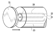
図13に、光ファイバ端面をフェルール端面よりも凹ませる方法の第1例を示す。直径が光ファイバの直径よりやや小さい120μm程度、高さ2μm程度の円柱状の凸型の突起を有する治具71を作製しておく。光ファイバ22をフェルール23に挿入して、光ファイバの端面とフェルールの端面とを面一にした後、光ファイバ22の端面を治具71の突起に当て、フェルール23の先端が治具71に突き当たるまで押し込み、光ファイバ22をフェルール23に固定する。このようにして、常に一定の長さだけ、光ファイバ端面をフェルール端面の奥に固定することができる。
図14に、光ファイバ端面をフェルール端面よりも凹ませる方法の第2例を示す。図14(a)に示したように、光ファイバ22をフェルール23に挿入し、通常のPC研磨またはAPC研磨を行う。この状態では、フェルール23の先端から光ファイバ22が凸形状に突出している。次に、図14(b)に示したように、フェルール23の先端を、フッ酸72に浸けると、光ファイバの先端だけがエッチングされる。フッ酸72への浸漬時間を調整して、光ファイバ端面が、フェルール端面から2μm程度奥まった位置になるように加工する。
図15に、光ファイバ端面をフェルール端面よりも凹ませる方法の第3例を示す。第2例と同様に、PC研磨またはAPC研磨を行った光ファイバ22とフェルール23とを用意する。これを、酸化セリウム研磨紙73で研磨すると、光ファイバの端面は削られ、フェルールの端面は削れないので、光ファイバの先端だけが凹む(図15(a))。酸化セリウム研磨剤を加えることにより、さらにこの効果は促進される。あるいは研磨用の起毛フィルムに酸化セリウム粉末を乗せて、純水で研磨する。このようにして、光ファイバ端面が、フェルール端面から2μm程度奥まった位置になるように加工する。図15(b)に、フェルール先端の形状を観測した結果を示す。
(試験結果)
図16に、本実施形態の光コネクタを用いた挿抜試験の結果を示す。55℃の恒温槽内で、波長405nm、50mWの光を通光し、光コネクタを抜き挿ししながら、伝送ロスを測定した結果を示す。環境温度を55℃に上げた加速試験を実施することにより、室温の場合と比べて、2~3倍劣化が早くなる。
図16に、本実施形態の光コネクタを用いた挿抜試験の結果を示す。55℃の恒温槽内で、波長405nm、50mWの光を通光し、光コネクタを抜き挿ししながら、伝送ロスを測定した結果を示す。環境温度を55℃に上げた加速試験を実施することにより、室温の場合と比べて、2~3倍劣化が早くなる。
従来のSPC研磨を行っただけのFC型光コネクタの場合(図中の◇印)、通光から150時間~300時間で伝送ロスが急激に増大し、APC研磨を行った場合(図中の〇印)は、600時間程度経過すると伝送ロスが増大する。第1の実施形態の実施例1のように、光ファイバ端面をフェルール端面から奥まった位置にしてギャップを設けた場合(図中の■印)、500時間を超えると伝送ロスが増大する。
これらに対して、第2の実施形態の実施例2のように、保護膜としてSi3N4膜を形成した場合(図中の△印)、1200時間程度経過してから伝送ロスが増大する。さらに、実施例2のように、保護膜としてSi3N4膜を形成して、さらにギャップを設けた場合2000時間程度まで伝送ロスは増大しない。
このように、光ファイバ端面にSi3N4膜を形成することにより、伝送ロスの劣化が抑えられ、さらにギャップを設けることにより、伝送ロスの増大が抑えられる。Si3N4膜に代えて、アルミナ(Al2O3)膜を用いることもできる。アルミナ膜1.8μmの上に、SiO2(114nm)/SiN(21.5nm)/SiO2(86.5nm)からなる無反射コートを形成することにより、波長405nm付近で95%以上の透過率となる。
ここでは、Si3N4膜とAl2O3膜とを例示したが、Si、Mg、Al、Hf、Nb、Zr、Sc、Ta、Ga、Zn、Y、B、Ti等の酸化物(特に、SiO2、Nb2O5、TiO2、ZrO2等)、窒化物(特に、AlN、AlGaN、BN等)、またはフッ化物(特にMgF2,CaF2,BaF2、LiF)なども同様の効果を奏することができる。
膜の厚さは、0.5μm以上が必要であるが、3μm以上よりも厚くすると、膜にクラックが入ることにより、却って伝送ロスが増大する場合がある。従って、膜厚は0.5μm~3μmが最適である。ここでは、膜の形成にマグネトロンスパッタリングを使用したが、その他の形成方法(蒸着、CVD)でも可能である。また、膜質の向上のためには、ECRスパッタで形成した膜が最も効果が大きい。
[第3の実施形態]
コア端面の間にスペーサを挿入する構造である。
コア端面の間にスペーサを挿入する構造である。
(実施例7)
図17に、実施例7にかかる可視光から紫外光用のシングルモード光ファイバを接続するための光コネクタの構造を示す。シングルモードのコア21a,21bを含む光ファイバ22a,22bがフェルール83a,83bに固定され、フェルール83a,83bをスリーブ25に挿入して突き合わせる。光ファイバ22a,22bは、可視光(405nm)用の純粋石英コアファイバである。
図17に、実施例7にかかる可視光から紫外光用のシングルモード光ファイバを接続するための光コネクタの構造を示す。シングルモードのコア21a,21bを含む光ファイバ22a,22bがフェルール83a,83bに固定され、フェルール83a,83bをスリーブ25に挿入して突き合わせる。光ファイバ22a,22bは、可視光(405nm)用の純粋石英コアファイバである。
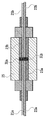
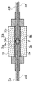
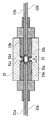
光ファイバ22a,22bの端面は、フェルール83a,83bの端面と面一であり、両端面には、厚さ1.8μmのSi3N4膜81a,81bが、スパッタリングにより形成されている。コア端面の間にギャップを設けるために、厚さ10μmの金属箔からなるスペーサ84を置く。スペーサ84は、図17(b)に示すように、円盤状の中央に光を通過ために穴があいており、厚さ1μm程度の光学接着剤82a-82dにより、一方のフェルール83bの端面に固定されている。
このようにして一対のフェルール83a,83bをスリーブ25に差し込むと、スペーサ84の分だけコア端面の間にギャップGが生じて、光ファイバ同士が接触することがなくなる。このため、実施例1と同様に可視光を通光した状態で光コネクタを抜き挿ししても、伝送ロスの変動は見られなかった。
Claims (10)
- 波長650nm以下の可視光から紫外光用のシングルモード光ファイバを接続するための光コネクタであって、前記光ファイバが固定されたフェルールをスリーブに挿入して突き合わせ、前記光ファイバを接続する光コネクタにおいて、
前記光ファイバおよび前記フェルールの端面には、窒化物、酸化物またはフッ化物からなる膜が形成されていることを特徴とする光コネクタ。 - 少なくとも一方の前記光ファイバの端面は、前記フェルールの端面から奥まった位置にあり、前記フェルールを前記スリーブに挿入したとき、前記光ファイバの端面間にギャップができることを特徴とする請求項1に記載の光コネクタ。
- 前記膜の上に、さらに無反射コートが形成されていることを特徴とする請求項2に記載の光コネクタ。
- 前記ギャップには、シリコーンオイルまたはシリコーンゲルが充填されていることを特徴とする請求項2または3に記載の光コネクタ。
- 少なくとも一方の前記光ファイバの端面は、光軸に対して傾いていることを特徴とする請求項1ないし4のいずれか1項に記載の光コネクタ。
- 前記膜は、前記フェルール内の前記光ファイバの側面に形成されていることを特徴とする請求項1ないし5のいずれか1項に記載の光コネクタ。
- 波長650nm以下の可視光から紫外光用のシングルモード光ファイバを接続するための光コネクタであって、前記光ファイバが固定されたフェルールをスリーブに挿入して突き合わせ、前記光ファイバを接続する光コネクタにおいて、
前記光ファイバの端面と前記フェルールの端面とは面一であり、前記フェルールの端面間にスペーサが挿入され、前記光ファイバの端面間にギャップができることを特徴とする光コネクタ。 - 波長650nm以下の可視光から紫外光用のシングルモード光ファイバを接続するための光コネクタの製造方法であって、
前記光ファイバをフェルールに挿入して、前記光ファイバの端面と前記フェルールの端面とを面一にする工程と、
前記光ファイバの端面を、直径が前記光ファイバの直径より小さい円柱状の凸型の突起を有する治具の前記突起に当て、前記フェルールを前記治具に突き当てる工程と、
前記光ファイバを前記フェルールに固定する工程と
を備えたことを特徴とする光コネクタの製造方法。 - 波長650nm以下の可視光から紫外光用のシングルモード光ファイバを接続するための光コネクタの製造方法であって、
前記光ファイバをフェルールに挿入して、前記光ファイバを前記フェルールに固定する工程と、
前記光ファイバの先端を研磨する工程と、
前記光ファイバの端面を、フッ酸に浸漬してエッチングし、前記光ファイバの端面が前記フェルールの端面から奥まった位置にあるように加工する工程と
を備えたことを特徴とする光コネクタの製造方法。 - 波長650nm以下の可視光から紫外光用のシングルモード光ファイバを接続するための光コネクタの製造方法であって、
前記光ファイバをフェルールに挿入して、前記光ファイバを前記フェルールに固定する工程と、
前記光ファイバの先端を研磨する工程と、
前記光ファイバの端面を、酸化セリウムで研磨し、前記光ファイバの端面が前記フェルールの端面から奥まった位置にあるように加工する工程と
を備えたことを特徴とする光コネクタの製造方法。
Priority Applications (2)
| Application Number | Priority Date | Filing Date | Title |
|---|---|---|---|
| JP2020565585A JPWO2020144909A1 (ja) | 2019-01-08 | 2019-10-17 | 光コネクタおよびその製造方法 |
| US17/418,572 US20220075120A1 (en) | 2019-01-08 | 2019-10-17 | Optical fiber and manufacturing method thereof |
Applications Claiming Priority (2)
| Application Number | Priority Date | Filing Date | Title |
|---|---|---|---|
| JP2019-001373 | 2019-01-08 | ||
| JP2019001373 | 2019-01-08 |
Publications (1)
| Publication Number | Publication Date |
|---|---|
| WO2020144909A1 true WO2020144909A1 (ja) | 2020-07-16 |
Family
ID=71520344
Family Applications (1)
| Application Number | Title | Priority Date | Filing Date |
|---|---|---|---|
| PCT/JP2019/040819 Ceased WO2020144909A1 (ja) | 2019-01-08 | 2019-10-17 | 光コネクタおよびその製造方法 |
Country Status (3)
| Country | Link |
|---|---|
| US (1) | US20220075120A1 (ja) |
| JP (1) | JPWO2020144909A1 (ja) |
| WO (1) | WO2020144909A1 (ja) |
Cited By (2)
| Publication number | Priority date | Publication date | Assignee | Title |
|---|---|---|---|---|
| CN115670354A (zh) * | 2021-07-27 | 2023-02-03 | 深圳迈瑞生物医疗电子股份有限公司 | 一种光学连接器和内窥镜摄像系统 |
| JP2023117011A (ja) * | 2022-02-10 | 2023-08-23 | 大学共同利用機関法人自然科学研究機構 | 光ファイバーおよび光ファイバーの製造方法 |
Families Citing this family (1)
| Publication number | Priority date | Publication date | Assignee | Title |
|---|---|---|---|---|
| JP2024066829A (ja) * | 2022-11-02 | 2024-05-16 | 住友電気工業株式会社 | 光コネクタ、光コネクタの製造方法、及び光接続構造 |
Citations (10)
| Publication number | Priority date | Publication date | Assignee | Title |
|---|---|---|---|---|
| JPS59158103U (ja) * | 1983-04-07 | 1984-10-23 | 三菱電線工業株式会社 | 光フアイバケ−ブル |
| JPH0519139A (ja) * | 1991-07-12 | 1993-01-29 | Citizen Watch Co Ltd | 光コネクタおよびその端面加工方法 |
| JP2002048943A (ja) * | 2000-08-07 | 2002-02-15 | Furukawa Electric Co Ltd:The | 光ファイバの先端位置調整部材およびそれを用いた光コネクタ組み立て装置 |
| JP2005181693A (ja) * | 2003-12-19 | 2005-07-07 | Pilot Precision Co Ltd | 光コネクタと、その製造方法およびそれに用いる研削治具 |
| JP2008250183A (ja) * | 2007-03-30 | 2008-10-16 | Fujifilm Corp | 光デバイス |
| JP2011118044A (ja) * | 2009-12-01 | 2011-06-16 | Anritsu Corp | ファイバファブリペローエタロンとその製造方法、外部共振器型半導体レーザ、ラマン増幅器 |
| JP2012008473A (ja) * | 2010-06-28 | 2012-01-12 | Yazaki Corp | 中継光コネクタ |
| JP2017054110A (ja) * | 2015-09-09 | 2017-03-16 | 日本電信電話株式会社 | 光モジュール |
| JP2017078819A (ja) * | 2015-10-22 | 2017-04-27 | タイコエレクトロニクスジャパン合同会社 | 光コネクタ |
| WO2018113887A2 (en) * | 2016-12-20 | 2018-06-28 | 3Dintegrated Aps | A medical probe assembly |
Family Cites Families (8)
| Publication number | Priority date | Publication date | Assignee | Title |
|---|---|---|---|---|
| US4421383A (en) * | 1980-01-17 | 1983-12-20 | Gte Laboratories Incorporated | Optical fiber connectors |
| JP2001174666A (ja) * | 1999-12-17 | 2001-06-29 | Furukawa Electric Co Ltd:The | 光フェルール |
| JP3802766B2 (ja) * | 2000-03-21 | 2006-07-26 | 古河電気工業株式会社 | 光デバイス製造方法と光デバイス |
| JP4963375B2 (ja) * | 2005-11-02 | 2012-06-27 | 富士フイルム株式会社 | 光デバイス、光学部材及びライトガイド |
| AU2017228859B2 (en) * | 2016-03-10 | 2022-03-03 | Corning Optical Communications LLC | Ferrule-based fiber optic connectors with ferrule retraction balancing |
| US9989709B2 (en) * | 2016-05-23 | 2018-06-05 | The Boeing Company | Method for polishing end faces of plastic optical fiber |
| JP2018194669A (ja) * | 2017-05-17 | 2018-12-06 | コニカミノルタ株式会社 | 光学素子及び光コネクタ |
| JP6543321B2 (ja) * | 2017-12-01 | 2019-07-10 | 株式会社フジクラ | 光コネクタ及び光コネクタの接続方法 |
-
2019
- 2019-10-17 WO PCT/JP2019/040819 patent/WO2020144909A1/ja not_active Ceased
- 2019-10-17 US US17/418,572 patent/US20220075120A1/en not_active Abandoned
- 2019-10-17 JP JP2020565585A patent/JPWO2020144909A1/ja active Pending
Patent Citations (10)
| Publication number | Priority date | Publication date | Assignee | Title |
|---|---|---|---|---|
| JPS59158103U (ja) * | 1983-04-07 | 1984-10-23 | 三菱電線工業株式会社 | 光フアイバケ−ブル |
| JPH0519139A (ja) * | 1991-07-12 | 1993-01-29 | Citizen Watch Co Ltd | 光コネクタおよびその端面加工方法 |
| JP2002048943A (ja) * | 2000-08-07 | 2002-02-15 | Furukawa Electric Co Ltd:The | 光ファイバの先端位置調整部材およびそれを用いた光コネクタ組み立て装置 |
| JP2005181693A (ja) * | 2003-12-19 | 2005-07-07 | Pilot Precision Co Ltd | 光コネクタと、その製造方法およびそれに用いる研削治具 |
| JP2008250183A (ja) * | 2007-03-30 | 2008-10-16 | Fujifilm Corp | 光デバイス |
| JP2011118044A (ja) * | 2009-12-01 | 2011-06-16 | Anritsu Corp | ファイバファブリペローエタロンとその製造方法、外部共振器型半導体レーザ、ラマン増幅器 |
| JP2012008473A (ja) * | 2010-06-28 | 2012-01-12 | Yazaki Corp | 中継光コネクタ |
| JP2017054110A (ja) * | 2015-09-09 | 2017-03-16 | 日本電信電話株式会社 | 光モジュール |
| JP2017078819A (ja) * | 2015-10-22 | 2017-04-27 | タイコエレクトロニクスジャパン合同会社 | 光コネクタ |
| WO2018113887A2 (en) * | 2016-12-20 | 2018-06-28 | 3Dintegrated Aps | A medical probe assembly |
Cited By (3)
| Publication number | Priority date | Publication date | Assignee | Title |
|---|---|---|---|---|
| CN115670354A (zh) * | 2021-07-27 | 2023-02-03 | 深圳迈瑞生物医疗电子股份有限公司 | 一种光学连接器和内窥镜摄像系统 |
| JP2023117011A (ja) * | 2022-02-10 | 2023-08-23 | 大学共同利用機関法人自然科学研究機構 | 光ファイバーおよび光ファイバーの製造方法 |
| JP7837015B2 (ja) | 2022-02-10 | 2026-03-30 | 大学共同利用機関法人自然科学研究機構 | 光ファイバーおよび光ファイバーの製造方法 |
Also Published As
| Publication number | Publication date |
|---|---|
| JPWO2020144909A1 (ja) | 2021-10-14 |
| US20220075120A1 (en) | 2022-03-10 |
Similar Documents
| Publication | Publication Date | Title |
|---|---|---|
| US12535640B2 (en) | Optical fiber termination structure, optical connection component and hollow-core optical fiber | |
| Komanec et al. | Low-loss and low-back-reflection hollow-core to standard fiber interconnection | |
| US7020364B2 (en) | Permanent light coupling arrangement and method for use with thin silicon optical waveguides | |
| US20090232450A1 (en) | Simple fiber optic cavity | |
| US20110085772A1 (en) | Buffered Large Core Fiber | |
| JPWO2020144909A1 (ja) | 光コネクタおよびその製造方法 | |
| US10634846B2 (en) | Optical module | |
| JP2988515B2 (ja) | 光導波路 | |
| US7801186B2 (en) | Light source | |
| JP5711832B1 (ja) | 光コネクタおよびその作製方法 | |
| US8998507B2 (en) | Fiber optic connectors and structures for optical fibers and methods for using the same | |
| US12504583B2 (en) | Terminated hollow-core fiber with suspended fiber-end | |
| JP2004126563A (ja) | レンズ一体型光ファイバとその製造方法 | |
| US11988873B2 (en) | End structure of a waveguide | |
| US11237334B2 (en) | Fiber module | |
| US6041156A (en) | Optical connection | |
| JP2004205662A (ja) | 光デバイスと光ファイバの結合方法及び光デバイス | |
| JP2808858B2 (ja) | 光ファイバ端の無反射処理方法および光ファイバ無反射端 | |
| JP2008250184A (ja) | ファイバ光源装置 | |
| JP2012163802A (ja) | ファイバヒューズストッパ、光コネクタ、光伝送システム、及びファイバヒューズ停止方法 | |
| JP2006011119A (ja) | 光部品、波長合分波器および光部品の製造方法 | |
| WO2018049312A1 (en) | Thin film anti-reflection coating for optical fibers in contact | |
| JP2008250183A (ja) | 光デバイス | |
| WO2026096059A1 (en) | Monolithic mode field adapter and coupler | |
| JP2000356725A (ja) | 偏光依存性損失(pdl)を低減した光学境界面を有する測定装置 |
Legal Events
| Date | Code | Title | Description |
|---|---|---|---|
| 121 | Ep: the epo has been informed by wipo that ep was designated in this application |
Ref document number: 19909224 Country of ref document: EP Kind code of ref document: A1 |
|
| ENP | Entry into the national phase |
Ref document number: 2020565585 Country of ref document: JP Kind code of ref document: A |
|
| NENP | Non-entry into the national phase |
Ref country code: DE |
|
| 122 | Ep: pct application non-entry in european phase |
Ref document number: 19909224 Country of ref document: EP Kind code of ref document: A1 |