WO2020138330A1 - ヒータ - Google Patents
ヒータ Download PDFInfo
- Publication number
- WO2020138330A1 WO2020138330A1 PCT/JP2019/051224 JP2019051224W WO2020138330A1 WO 2020138330 A1 WO2020138330 A1 WO 2020138330A1 JP 2019051224 W JP2019051224 W JP 2019051224W WO 2020138330 A1 WO2020138330 A1 WO 2020138330A1
- Authority
- WO
- WIPO (PCT)
- Prior art keywords
- conductor
- metal particles
- ceramics
- heater according
- metal
- Prior art date
- Legal status (The legal status is an assumption and is not a legal conclusion. Google has not performed a legal analysis and makes no representation as to the accuracy of the status listed.)
- Ceased
Links
Images





Classifications
-
- H—ELECTRICITY
- H05—ELECTRIC TECHNIQUES NOT OTHERWISE PROVIDED FOR
- H05B—ELECTRIC HEATING; ELECTRIC LIGHT SOURCES NOT OTHERWISE PROVIDED FOR; CIRCUIT ARRANGEMENTS FOR ELECTRIC LIGHT SOURCES, IN GENERAL
- H05B3/00—Ohmic-resistance heating
- H05B3/10—Heating elements characterised by the composition or nature of the materials or by the arrangement of the conductor
- H05B3/12—Heating elements characterised by the composition or nature of the materials or by the arrangement of the conductor characterised by the composition or nature of the conductive material
- H05B3/14—Heating elements characterised by the composition or nature of the materials or by the arrangement of the conductor characterised by the composition or nature of the conductive material the material being non-metallic
- H05B3/141—Conductive ceramics, e.g. metal oxides, metal carbides, barium titanate, ferrites, zirconia, vitrous compounds
-
- H—ELECTRICITY
- H05—ELECTRIC TECHNIQUES NOT OTHERWISE PROVIDED FOR
- H05B—ELECTRIC HEATING; ELECTRIC LIGHT SOURCES NOT OTHERWISE PROVIDED FOR; CIRCUIT ARRANGEMENTS FOR ELECTRIC LIGHT SOURCES, IN GENERAL
- H05B3/00—Ohmic-resistance heating
- H05B3/20—Heating elements having extended surface area substantially in a two-dimensional [2D] plane, e.g. plate-heater
- H05B3/22—Heating elements having extended surface area substantially in a two-dimensional [2D] plane, e.g. plate-heater non-flexible
- H05B3/26—Heating elements having extended surface area substantially in a two-dimensional [2D] plane, e.g. plate-heater non-flexible heating conductor mounted on insulating base
- H05B3/265—Heating elements having extended surface area substantially in a two-dimensional [2D] plane, e.g. plate-heater non-flexible heating conductor mounted on insulating base the insulating base being an inorganic material, e.g. ceramic
-
- H—ELECTRICITY
- H05—ELECTRIC TECHNIQUES NOT OTHERWISE PROVIDED FOR
- H05B—ELECTRIC HEATING; ELECTRIC LIGHT SOURCES NOT OTHERWISE PROVIDED FOR; CIRCUIT ARRANGEMENTS FOR ELECTRIC LIGHT SOURCES, IN GENERAL
- H05B3/00—Ohmic-resistance heating
- H05B3/02—Details
-
- H—ELECTRICITY
- H05—ELECTRIC TECHNIQUES NOT OTHERWISE PROVIDED FOR
- H05B—ELECTRIC HEATING; ELECTRIC LIGHT SOURCES NOT OTHERWISE PROVIDED FOR; CIRCUIT ARRANGEMENTS FOR ELECTRIC LIGHT SOURCES, IN GENERAL
- H05B2203/00—Aspects relating to Ohmic resistive heating covered by group H05B3/00
- H05B2203/002—Heaters using a particular layout for the resistive material or resistive elements
- H05B2203/003—Heaters using a particular layout for the resistive material or resistive elements using serpentine layout
-
- H—ELECTRICITY
- H05—ELECTRIC TECHNIQUES NOT OTHERWISE PROVIDED FOR
- H05B—ELECTRIC HEATING; ELECTRIC LIGHT SOURCES NOT OTHERWISE PROVIDED FOR; CIRCUIT ARRANGEMENTS FOR ELECTRIC LIGHT SOURCES, IN GENERAL
- H05B2203/00—Aspects relating to Ohmic resistive heating covered by group H05B3/00
- H05B2203/013—Heaters using resistive films or coatings
-
- H—ELECTRICITY
- H05—ELECTRIC TECHNIQUES NOT OTHERWISE PROVIDED FOR
- H05B—ELECTRIC HEATING; ELECTRIC LIGHT SOURCES NOT OTHERWISE PROVIDED FOR; CIRCUIT ARRANGEMENTS FOR ELECTRIC LIGHT SOURCES, IN GENERAL
- H05B2203/00—Aspects relating to Ohmic resistive heating covered by group H05B3/00
- H05B2203/017—Manufacturing methods or apparatus for heaters
-
- H—ELECTRICITY
- H05—ELECTRIC TECHNIQUES NOT OTHERWISE PROVIDED FOR
- H05B—ELECTRIC HEATING; ELECTRIC LIGHT SOURCES NOT OTHERWISE PROVIDED FOR; CIRCUIT ARRANGEMENTS FOR ELECTRIC LIGHT SOURCES, IN GENERAL
- H05B2203/00—Aspects relating to Ohmic resistive heating covered by group H05B3/00
- H05B2203/021—Heaters specially adapted for heating liquids
Definitions
- the present disclosure relates to a heater.
- a heater in which a ceramic, which is an insulator, is used as a base and a conductor as a heating element is formed on the surface of the base is widely used in various fields.
- Patent Document 1 discloses a ceramic heater in which a heating element pattern including a heating portion and a lead portion is formed on the surface of a ceramic insulating layer.
- the heater of the present disclosure is made of ceramics and has a base body having a first surface and a first electric conductor having a void and located on the first surface.
- the heater of the present disclosure is less likely to crack the base even if heating and cooling are repeated. Therefore, it can be used for a long period of time.
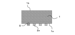
- FIG. 3 is an example of a rear view of a heater according to the present disclosure.
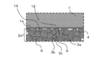
- FIG. 2 is a sectional view taken along the line A-A′ in FIG. 1. It is an example of the enlarged view in the S section shown in FIG.
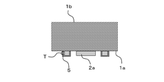
- FIG. 2 is a sectional view taken along line B-B′ in FIG. 1.
- 6 is another example of a cross-sectional view taken along the line B-B′ of FIG. 1.
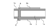
- FIG. 2 is a sectional view taken along the line C-C′ of FIG. 1.
- 9 is another example of a cross-sectional view taken along the line C-C′ of FIG. 1.
- FIG. 1 is an example of a rear view of the heater 10 of the present disclosure, specifically, a view looking toward the first surface 1 a of the heater 10.
- FIG. 2 is a cross-sectional view taken along the line AA′ of FIG.
- the heater 10 of the present disclosure includes a base 1 having a first surface 1a and a first conductor 2a on the first surface 1a, and allows electricity to flow through the first conductor 2a.
- the object to be heated can be heated by.
- the 2nd surface 1b is located in the opposite of the 1st surface 1a, and this surface is a surface near a heating target object, for example, is a mounting surface of a heating target object.
- the fact that the first conductor 2a is located on the first surface 1a means that the first conductor 2a is located on the surface of the first surface 1a.
- the base body 1 of the heater 10 of the present disclosure is made of ceramics.
- ceramics include aluminum oxide ceramics, silicon carbide ceramics, cordierite ceramics, silicon nitride ceramics, aluminum nitride ceramics, and mullite ceramics.
- the substrate 1 is made of aluminum oxide ceramics, it is excellent in workability and inexpensive.
- the aluminum oxide ceramics are those containing 70% by mass or more of aluminum oxide in 100% by mass of all components constituting the ceramics.
- the material of the substrate 1 in the heater 10 of the present disclosure can be confirmed by the following method. First, the substrate 1 is measured using an X-ray diffractometer (XRD), and identification is performed using a JCPDS card from the value of 2 ⁇ (2 ⁇ is the diffraction angle) obtained. Next, the contained components are quantitatively analyzed using a fluorescent X-ray analyzer (XRF).
- XRD X-ray diffractometer
- XRF fluorescent X-ray analyzer
- the coefficient of thermal expansion of ceramics is about 7.2 ppm for aluminum oxide ceramics, about 3.7 ppm for silicon carbide ceramics, about 1.5 ppm for cordierite ceramics, and 2. 5 for silicon nitride ceramics.
- FIGS. 1 and 2 show an example in which the base body 1 has a rectangular plate shape and has a first surface 1a and a second surface 1b facing the first surface 1a.
- the shape is not limited to this, and may have any shape.
- the first conductor 2a may be located on the first surface 1a of the base 1 in any arrangement.
- FIG. 3 is an enlarged view of part S shown in FIG.
- the first conductor 2a in the heater 10 of the present disclosure has a plurality of voids 9.
- the first conductor 2a may include first metal particles 3a and second metal particles 3b.
- the voids 9 may be located between the first metal particles 3a and the second metal particles 3b.
- the first conductor 2a has a void 9. Therefore, the surface area of the first conductor 2a is larger than that of the conductor layer having no void 9. Therefore, the heater 10 has high heat dissipation.
- the first conductor 2a may include first metal particles 3a and second metal particles 3b.
- the voids 9 may be located between the first metal particles 3a and the second metal particles 3b. In the case of having such a configuration, the heat generated in the first metal particles 3a and the second metal particles 3b is absorbed in the voids 9, so that the heater 10 has high heat dissipation.
- the material of the first metal particles 3a and the second metal particles 3b constituting the first conductor 2a may be metal, but may be, for example, stainless steel, aluminum or copper.
- the coefficients of thermal expansion of these are generally about 10 to 18 ppm for stainless steel, about 23 ppm for aluminum, and about 16.7 ppm for copper.
- the shapes of the first metal particles 3a and the second metal particles 3b may be, for example, spherical, granular, whisker-shaped or needle-shaped.
- the first metal particles 3a and the second metal particles 3b may be bent.
- the first metal particles 3a and the second metal particles 3b may have corners.
- the length of the first metal particles 3a and the second metal particles 3b in the longitudinal direction may be 0.5 ⁇ m or more and 200 ⁇ m or less. ..
- the width may be 1 ⁇ m or more and 100 ⁇ m or less, and the length may be 100 ⁇ m or more and 5 mm or less.
- the first metal particles 3a and the second metal particles 3b are granular.
- the first metal particles 3a and the second metal particles 3b are whisker-shaped.
- FIG. 1 shows an example in which the first conductor 2a has a meandering shape
- the shape is not limited to this, and any shape may be used.
- the average thickness of the first conductor 2a may be, for example, 1 ⁇ m or more and 5 mm or less.
- the porosity of the first conductor 2a may be, for example, 10% or more and 90% or less.
- the porosity is an index representing the ratio of the voids 9 in the first conductor 2a.
- the porosity of the first conductor 2a may be calculated, for example, by measuring using the Archimedes method.
- the first conductor 2a may include third metal particles 3c.
- the first conductor 2a may have a welded portion 12 between the first metal particles 3a and the third metal particles 3c. Since the first metal particles 3a and the third metal particles 3c are not merely in contact with each other but are welded to each other, heat is easily transferred between the first metal particles 3a and the third metal particles 3c. Therefore, the first conductor 2a as a whole has high heat conduction efficiency. Therefore, the heater 10 has high reliability.
- the heater 10 of the present disclosure may include a bonding layer 4 located between the first conductor 2a and the first surface 1a, as shown in FIG. If such a configuration is satisfied, the first conductor 2a is less likely to be peeled from the base body 1, and the stress generated due to the difference in thermal expansion is relieved by the bonding layer 4 so that the base body 1 is less likely to be cracked. .. Therefore, the heater 10 of the present disclosure can be used for a longer period of time.
- the average thickness of the bonding layer 5 may be, for example, 1 ⁇ m or more and 0.5 mm or less.
- the bonding layer 4 in the heater 10 of the present disclosure may be made of metal or glass.
- the metal may be, for example, nickel, platinum, SUS, aluminum, copper or the like, and the glass may be, for example, borosilicate glass or silicate glass. If such a configuration is satisfied, the bonding layer 4 firmly bonds the first conductor 2a and the base body 1 to each other, and the first conductor 2a is less likely to be peeled from the base body 1.
- the bonding layer 4 is made of glass
- the coefficient of thermal expansion of glass is between that of metal and ceramics, so that the stress caused by the difference in thermal expansion between the first conductor 2a and the substrate 1 is the bonding layer. 4 effectively relaxes, and the base 1 is less likely to crack.
- the bonding layer 4 in the heater 10 of the present disclosure may be made of porous ceramics.
- the porous ceramics for example, those having the same components as the ceramics constituting the substrate 1 may be used. If such a structure is satisfied, the first metal particles 3a forming the first conductor 2a enter the inside of the bonding layer 4 which is porous, so that the first conductor 2a and the bonding layer 4 are strongly bonded. Since the base 1 and the bonding layer 4 are both ceramics, the base 1 and the bonding layer 4 are firmly bonded. Therefore, the first conductor 2a is less likely to be peeled from the base 1.
- FIG. 4 is a sectional view taken along the line B-B′ in FIG. 1.
- the front end portion of the first conductor 2a in the heater 10 of the present disclosure may be covered with the protective layer 5.
- the tip portion of the first conductor 2a is a portion from the tip of the first conductor 2a to a length of 5 mm.
- being covered with the protective layer 5 means that the protective layer 5 is located in contact with the tip of the first conductor 2a so that the tip of the first conductor 2a is not exposed to the outside.
- the protective layer 5 protects the tip of the first conductor 2a, which is most likely to be stressed and damaged when heating and cooling are repeated. Therefore, the heater 10 of the present disclosure can be used for a longer period of time.
- the protective layer 5 may be in contact with the substrate 1. If such a configuration is satisfied, the protective layer 5 reduces the risk of the tip portion of the first conductor 2a peeling from the substrate 1.
- the protective layer 5 may be made of any material as long as the porosity is less than 5%. Further, as shown in FIG. 9, the protective layer 5 may include the first component 11.
- the first component 11 may consist of one selected from ceramics, resins, metals and glasses.
- the ceramics are, for example, aluminum oxide ceramics, silicon carbide ceramics, cordierite ceramics, silicon nitride ceramics, aluminum nitride ceramics or mullite ceramics
- the resin is, for example, silicone resin or
- the metal may be, for example, an imidoamide resin
- the metal may be, for example, nickel, platinum, copper, or the like
- the glass may be, for example, borosilicate glass or silicate glass.
- the tip end portion of the first conductor 2a in the heater 10 of the present disclosure has the first component 11 located between the first metal particles 3a and the second metal particles 3b. May be. If such a configuration is satisfied, the bonding between the first conductor 2a and the protective layer 5 becomes strong, and the protective layer 5 peels from the first conductor 2a when heating and cooling are repeated. The risk is reduced.
- FIG. 5 shows another example of the cross-sectional view taken along the line B-B′ of FIG. 1.
- the heater 10 of the present disclosure may include the power supply terminal 6, and at least a part of the power supply terminal 6 may be located inside the first conductor 2a.
- the power supply terminal 6 is connected to an external power source (not shown) and is for supplying a current to the first conductor 2a. Then, if such a configuration is satisfied, there is little possibility that the power supply terminal 6 will come off when heating and cooling are repeated, and the current can be stably supplied to the first conductor 2a.
- the metal particles 3 in the heater 10 of the present disclosure may be covered with the oxide film 13. If such a configuration is satisfied, when a cooling medium such as water is passed through the first conductor 2a to cool the first conductor 2a that has generated heat, the first conductor 2a and the first conductor 2a are cooled. The chemical reaction with the medium can be suppressed. Therefore, the reliability of the heater 10 of the present disclosure is improved.
- a cooling medium such as water
- the oxide film 13 may be an oxide of a metal forming the metal particles 3.
- FIG. 6 shows a cross-sectional view taken along the line C-C′ of FIG.
- the substrate 1 in the heater 10 of the present disclosure may have the flow path 7 inside. If such a configuration is satisfied, the fluid flowing in the flow path 7 can be heated by causing the first conductor 2a to generate heat. For example, as a chemical reaction device of the present disclosure, the fluid reacts by heating. It is possible to use the heater 10.
- FIG. 7 shows another example of the cross-sectional view taken along the line C-C′ of FIG. 1.
- the heater 10 of the present disclosure further includes a second conductor 2b and a connection conductor 8, the second conductor 2b is located on the second surface 1b, and the first conductor 2a and the first conductor 2a.
- the two conductors 2b may be electrically connected via the connection conductor 8. If such a configuration is satisfied, the first conductor 2a, the connecting conductor 8 and the second conductor 2b become one conductor, and the length of the conductor is extended on the limited surface of the substrate 1. It is possible to rapidly heat the substrate 1 by the conductor. If the substrate 1 has the flow path 7, the fluid flowing in the flow path 7 can be rapidly heated, and for example, the reaction due to the heating of the fluid can be effectively promoted.
- the second conductor 2b may have the void 9 like the first conductor 2a. Further, the bonding layer 4 described above may be located between the second conductor 2b and the second surface 1b.
- connection conductor 8 may be a metal, but may be the same metal as the metal particles 3 forming the first conductor 2a and the second conductor 2b. Further, the connection conductor 8 may have a void 9 like the first conductor 2a and the second conductor 2b.
- the connecting conductor 8 may have any shape, but if it is cylindrical, its diameter may be 0.3 mm or more and 2 mm or less. Further, the number of the connecting conductors 8 may be one or more, but the number of the connecting conductors 8 may be increased according to the magnitude of the current used.
- a sintering aid, a binder, a solvent and the like are added to the powder of the raw material (aluminum oxide, silicon nitride, etc.) as the main component, and the mixture is appropriately mixed to prepare a slurry.
- a green sheet is formed by a doctor blade method and punched by a die or laser-processed to obtain a green sheet having a desired shape.
- this slurry is spray-dried to obtain granulated granules.
- the granules are rolled to form a green sheet, which is punched by a die or laser-processed to obtain a green sheet having a desired shape.
- holes are formed in the green sheet to form a flow path by forming a green body by stacking multiple green sheets. You may. Further, a metal paste serving as a connection conductor may be embedded in the molded body.
- the molded body is fired to obtain a base body made of ceramics and having a first surface.
- a first conductor is formed on the first surface of the base.
- a mask of a desired shape made of porous resin is formed on the first surface.
- a mixed liquid prepared by mixing a plurality of metal particles including first metal particles and second metal particles made of stainless steel, aluminum or copper with a liquid such as water is prepared and poured into the space formed by this mask. ..
- the liquid mixture is evaporated to evaporate the liquid.
- the mask is burned out or the solvent is used to remove the mask, and the substrate is pressurized with a predetermined pressure, and then the substrate is heated or ultrasonic vibration is applied.
- the first conductor having voids can be obtained by removing the porous mask.
- first metal particles and the second metal particles can be bonded by heating the substrate after applying a predetermined pressure or applying ultrasonic vibration. Furthermore, after applying a predetermined pressure, the base body is heated or ultrasonic vibration is applied to form a welded portion between the first metal particles and the third metal particles.
- the bonding layer may be formed on the first surface, and then the first conductor may be formed on the bonding layer.
- the bonding layer is metal, glass, or porous ceramics.
- the bonding layer may be formed by sputtering after forming the mask, or by electroless plating or metallization.
- the bonding layer is glass or porous ceramics
- the bonding layer may be formed before forming the mask.
- glass and porous ceramics may be formed by applying a paste containing each of them as a main component to the first surface and heat-treating the paste. Further, since glass and porous ceramics are insulative, they may be formed so as to cover the entire first surface of the substrate. The porous ceramics can be easily bonded to the base as long as it has the same composition as the ceramics forming the base.
- the bonding layer is metal or glass
- the bonding layer is bonded to the first conductor by being wet.
- the bonding layer is porous ceramics
- the metal particles forming the first conductor enter the porous ceramics for bonding. If the bonding layer is a metal, the metal of the bonding layer and the metal particles forming the first conductor are bonded to each other by applying electricity to the bonding layer and the first conductor, and the bonding layer and the first conductor are connected to each other. Can also be joined.
- the first conductor is prepared in advance by the following method. First, for example, a mixed liquid prepared by mixing a plurality of metal particles made of stainless steel, aluminum, or copper with a liquid such as water is prepared and poured into a mold having the shape of the first conductor. Next, the liquid is evaporated by drying it.
- first metal particles and the second metal particles are bonded by applying a predetermined pressure and heating or applying ultrasonic vibration. Then, when taken out from the mold, a plurality of metal particles including the first metal particles and the second metal particles are welded to obtain a first conductor having voids.
- the first conductor may be manufactured by the following method. First, a plurality of metal particles including the first metal particles and the second metal particles are mixed with a binder, and then a molded body is manufactured by a mechanical press method. Next, the binder is evaporated by drying this molded body. Then, it heats or gives ultrasonic vibration. Thereby, the plurality of metal particles including the first metal particles and the second metal particles can be welded to each other. Thereby, a welded part can be formed between the first metal particles and the third metal particles. As a result, the first conductor having voids is obtained.
- the second conductor may be formed on the second surface of the base by the same method as the above-mentioned first conductor.
- the metal particles are subjected to oxidation treatment with a strong oxidant, heat treatment in an oxygen atmosphere, anodic oxidation treatment, etc.
- the oxide film 13 such as a dynamic film may be formed.
- the protective layer may be formed by applying a paste containing ceramics, resin, metal, and glass as the main components to the tip of the first conductor, followed by drying and heat treatment.
- the first component forming the protective layer can be present between the first metal particles and the second metal particles at the tip of the first conductor.
- a hole matching the shape of the power supply terminal may be opened at the tip of the first conductor, and the power supply terminal may be inserted into this hole. ..
- a member having a hole for inserting the power supply terminal is prepared, and the member is bonded so as to be in contact with the tip of the first conductor, or paste is applied to the tip of the first conductor and the power supply terminal. It can be formed by applying, drying and heat treatment.
- Base 1a First surface 1b: Second surface 2a: First conductor 2b: Second conductor 3a: First metal particle 3b: Second metal particle 3c: Third metal particle 4: Bonding layer 5: Protection Layer 6: Power supply terminal 7: Flow path 8: Connection conductor 9: Void 10: Heater 11: First component 12: Welded portion 13: Oxide film
Landscapes
- Chemical & Material Sciences (AREA)
- Engineering & Computer Science (AREA)
- Ceramic Engineering (AREA)
- Resistance Heating (AREA)
- Surface Heating Bodies (AREA)
Abstract
Description
1a:第1面
1b:第2面
2a:第1導電体
2b:第2導電体
3a:第1金属粒子
3b:第2金属粒子
3c:第3金属粒子
4:接合層
5:保護層
6:給電端子
7:流路
8:接続導体
9:空隙
10:ヒータ
11:第1成分
12:溶着部
13:酸化膜
Claims (16)
- セラミックスからなり、第1面を有する基体と、
前記第1面の上に位置する空隙を有する第1導電体と、を有しているヒータ。 - 前記第1導電体は、第1金属粒子と、第2金属粒子と、を有しており、
前記空隙は、前記第1金属粒子と前記第2金属粒子との間に位置する、請求項1に記載のヒータ。 - 前記第1導電体は、さらに第3金属粒子を有しており、
前記第1導電体は、前記第1金属粒子と、前記第3金属粒子との間に溶着部を有している、請求項2に記載のヒータ。 - 前記第1導電体および前記第1面の間に位置する接合層を有する、請求項1乃至3のいずれかに記載のヒータ。
- 前記接合層は、金属またはガラスからなる、請求項4に記載のヒータ。
- 前記接合層は、多孔質セラミックスからなる、請求項4に記載のヒータ。
- 前記第1導電体の先端部は、保護層に覆われている請求項1乃至請求項6のいずれかに記載のヒータ。
- 前記保護層は、第1成分を有しており、
前記第1導電体の先端部は、前記第1金属粒子と前記第2金属粒子との間に位置する前記第1成分を有する、請求項7に記載のヒータ。 - 給電端子を有し、該給電端子の少なくとも一部は、前記第1導電体の内部に位置している請求項7または請求項8に記載のヒータ。
- 前記第1金属粒子および前記第2金属粒子は、酸化膜で覆われている請求項1乃至請求項9のいずれかに記載のヒータ。
- 前記基体は、内部に流路を有する、請求項1乃至請求項10のいずれかに記載のヒータ。
- さらに第2導電体および接続導体を備え、
前記基体は、前記第1面に対向する第2面を有し、
前記第2導電体は、前記第2面上に位置し、
前記第1導電体および前記第2導電体は、前記接続導体を介して電気的に接続されている、請求項1乃至請求項11のいずれかに記載のヒータ。 - セラミックスからなり、第1面を有する基体を用意する第1ステップと、
前記第1面にマスクによって空間を形成する第2ステップと、
第1金属粒子および第2金属粒子を液体に混合した混合液を用意する第3ステップと、
前記マスクによって形成された空間に前記混合液を流し込む第4ステップと、
前記混合液を乾燥させることで液体を蒸発させる第5ステップと、
前記マスクを除去する第6ステップと、
前記第1金属粒子および前記第2金属粒子を加圧する第7ステップと、
前記第1金属粒子および前記第2金属粒子を加熱する第8ステップと、を有するヒータの製造方法。 - セラミックスからなり、第1面を有する基体を用意する第1ステップと、
前記第1面にマスクによって空間を形成する第2ステップと、
第1金属粒子および第2金属粒子を液体に混合した混合液を用意する第3ステップと、
前記マスクによって形成された空間に前記混合液を流し込む第4ステップと、
前記混合液を乾燥させることで液体を蒸発させる第5ステップと、
前記マスクを除去する第6ステップと、
前記第1金属粒子および前記第2金属粒子を加圧する第7ステップと、
前記第1金属粒子および前記第2金属粒子に超音波振動を与える第8ステップと、を有するヒータの製造方法。 - 第1金属粒子および第2金属粒子と、バインダと、を混ぜ合わせた混合液を用意する第1ステップと、
メカプレス法により前記混合液を成型体にする第2ステップと、
前記成形体を乾燥させることで前記バインダを蒸発させる第3ステップと、
前記成形体を加熱することで前記第1導電体を得る第4ステップと、
セラミックスからなり、第1面を有する基体を用意する第5ステップと、
前記第1面上に前記第1導電体を載置する第6ステップと、を有するヒータの製造方法。 - 第1金属粒子および第2金属粒子と、バインダと、を混ぜ合わせた混合液を用意する第1ステップと、
メカプレス法により前記混合液を成型体にする第2ステップと、
前記成形体を乾燥させることで前記バインダを蒸発させる第3ステップと、
前記成形体に超音波振動を与えることで前記第1導電体を得る第4ステップと、
セラミックスからなり、第1面を有する基体を用意する第5ステップと、
前記第1面上に前記第1導電体を載置する第6ステップと、を有するヒータの製造方法。
Priority Applications (3)
| Application Number | Priority Date | Filing Date | Title |
|---|---|---|---|
| KR1020217017493A KR20210087081A (ko) | 2018-12-26 | 2019-12-26 | 히터 및 히터의 제조 방법 |
| JP2020562431A JPWO2020138330A1 (ja) | 2018-12-26 | 2019-12-26 | ヒータ |
| US17/414,269 US20220070978A1 (en) | 2018-12-26 | 2019-12-26 | Heater |
Applications Claiming Priority (2)
| Application Number | Priority Date | Filing Date | Title |
|---|---|---|---|
| JP2018-242958 | 2018-12-26 | ||
| JP2018242958 | 2018-12-26 |
Publications (1)
| Publication Number | Publication Date |
|---|---|
| WO2020138330A1 true WO2020138330A1 (ja) | 2020-07-02 |
Family
ID=71129503
Family Applications (1)
| Application Number | Title | Priority Date | Filing Date |
|---|---|---|---|
| PCT/JP2019/051224 Ceased WO2020138330A1 (ja) | 2018-12-26 | 2019-12-26 | ヒータ |
Country Status (4)
| Country | Link |
|---|---|
| US (1) | US20220070978A1 (ja) |
| JP (1) | JPWO2020138330A1 (ja) |
| KR (1) | KR20210087081A (ja) |
| WO (1) | WO2020138330A1 (ja) |
Cited By (3)
| Publication number | Priority date | Publication date | Assignee | Title |
|---|---|---|---|---|
| CN116406950A (zh) * | 2021-12-31 | 2023-07-11 | 佛山市顺德区美的电热电器制造有限公司 | 发热组件、烹饪器具以及烹饪设备 |
| JP2023538982A (ja) * | 2021-07-27 | 2023-09-13 | ケーティー アンド ジー コーポレイション | エアロゾル生成用面状発熱体、この製造方法及びこれを含むエアロゾル発生装置 |
| US12478101B2 (en) | 2022-03-31 | 2025-11-25 | Hainan Moore Brothers Technology Co., Ltd. | Electronic vaporization device and vaporization core thereof |
Families Citing this family (1)
| Publication number | Priority date | Publication date | Assignee | Title |
|---|---|---|---|---|
| CN114847532A (zh) * | 2022-03-31 | 2022-08-05 | 海南摩尔兄弟科技有限公司 | 电子雾化装置及其雾化芯 |
Citations (10)
| Publication number | Priority date | Publication date | Assignee | Title |
|---|---|---|---|---|
| JPS62285391A (ja) * | 1986-06-03 | 1987-12-11 | 株式会社 サ−モミツク | 面状発熱体 |
| JPH0511386U (ja) * | 1991-07-26 | 1993-02-12 | 京セラ株式会社 | セラミツクヒータ |
| JPH05144553A (ja) * | 1991-11-25 | 1993-06-11 | Matsushita Electric Works Ltd | ヒータおよびヒータの製造方法 |
| JPH11135241A (ja) * | 1997-10-29 | 1999-05-21 | Kyocera Corp | 流体加熱用のセラミックヒータ |
| JP2003109728A (ja) * | 2001-09-28 | 2003-04-11 | Matsushita Electric Ind Co Ltd | 印刷ヒータ |
| JP2003133225A (ja) * | 2002-07-15 | 2003-05-09 | Ibiden Co Ltd | 半導体製品加熱用ヒータ |
| JP2012048949A (ja) * | 2010-08-26 | 2012-03-08 | Hitachi Maxell Ltd | 金担持粒子及びその製造方法、並びにその金担持粒子を用いた導電性膜及びその製造方法 |
| WO2014175424A1 (ja) * | 2013-04-27 | 2014-10-30 | 京セラ株式会社 | セラミックヒータ |
| JP2014216221A (ja) * | 2013-04-26 | 2014-11-17 | 京セラ株式会社 | ヒータ |
| JP2015011900A (ja) * | 2013-06-28 | 2015-01-19 | 古河電気工業株式会社 | 導電性ペースト、及びその製造方法 |
Family Cites Families (2)
| Publication number | Priority date | Publication date | Assignee | Title |
|---|---|---|---|---|
| WO2001067819A1 (en) * | 2000-03-03 | 2001-09-13 | Cooper Richard P | Thin film tubular heater |
| JP3929882B2 (ja) | 2002-11-26 | 2007-06-13 | 京セラ株式会社 | 平板状セラミックヒータおよびこれを用いた検出素子 |
-
2019
- 2019-12-26 JP JP2020562431A patent/JPWO2020138330A1/ja active Pending
- 2019-12-26 WO PCT/JP2019/051224 patent/WO2020138330A1/ja not_active Ceased
- 2019-12-26 KR KR1020217017493A patent/KR20210087081A/ko not_active Withdrawn
- 2019-12-26 US US17/414,269 patent/US20220070978A1/en not_active Abandoned
Patent Citations (10)
| Publication number | Priority date | Publication date | Assignee | Title |
|---|---|---|---|---|
| JPS62285391A (ja) * | 1986-06-03 | 1987-12-11 | 株式会社 サ−モミツク | 面状発熱体 |
| JPH0511386U (ja) * | 1991-07-26 | 1993-02-12 | 京セラ株式会社 | セラミツクヒータ |
| JPH05144553A (ja) * | 1991-11-25 | 1993-06-11 | Matsushita Electric Works Ltd | ヒータおよびヒータの製造方法 |
| JPH11135241A (ja) * | 1997-10-29 | 1999-05-21 | Kyocera Corp | 流体加熱用のセラミックヒータ |
| JP2003109728A (ja) * | 2001-09-28 | 2003-04-11 | Matsushita Electric Ind Co Ltd | 印刷ヒータ |
| JP2003133225A (ja) * | 2002-07-15 | 2003-05-09 | Ibiden Co Ltd | 半導体製品加熱用ヒータ |
| JP2012048949A (ja) * | 2010-08-26 | 2012-03-08 | Hitachi Maxell Ltd | 金担持粒子及びその製造方法、並びにその金担持粒子を用いた導電性膜及びその製造方法 |
| JP2014216221A (ja) * | 2013-04-26 | 2014-11-17 | 京セラ株式会社 | ヒータ |
| WO2014175424A1 (ja) * | 2013-04-27 | 2014-10-30 | 京セラ株式会社 | セラミックヒータ |
| JP2015011900A (ja) * | 2013-06-28 | 2015-01-19 | 古河電気工業株式会社 | 導電性ペースト、及びその製造方法 |
Cited By (4)
| Publication number | Priority date | Publication date | Assignee | Title |
|---|---|---|---|---|
| JP2023538982A (ja) * | 2021-07-27 | 2023-09-13 | ケーティー アンド ジー コーポレイション | エアロゾル生成用面状発熱体、この製造方法及びこれを含むエアロゾル発生装置 |
| JP7568739B2 (ja) | 2021-07-27 | 2024-10-16 | ケーティー アンド ジー コーポレイション | エアロゾル生成用面状発熱体、この製造方法及びこれを含むエアロゾル発生装置 |
| CN116406950A (zh) * | 2021-12-31 | 2023-07-11 | 佛山市顺德区美的电热电器制造有限公司 | 发热组件、烹饪器具以及烹饪设备 |
| US12478101B2 (en) | 2022-03-31 | 2025-11-25 | Hainan Moore Brothers Technology Co., Ltd. | Electronic vaporization device and vaporization core thereof |
Also Published As
| Publication number | Publication date |
|---|---|
| US20220070978A1 (en) | 2022-03-03 |
| JPWO2020138330A1 (ja) | 2021-10-14 |
| KR20210087081A (ko) | 2021-07-09 |
Similar Documents
| Publication | Publication Date | Title |
|---|---|---|
| WO2020138330A1 (ja) | ヒータ | |
| CN101304017B (zh) | 烧结的功率半导体基片及其制造方法 | |
| CN108851461A (zh) | 加热器 | |
| CN114097075B (zh) | 陶瓷基板、电路基板及其制造方法、以及功率模块 | |
| JP5258480B2 (ja) | セラミックヒータ | |
| JPWO2011034075A1 (ja) | セラミックス回路基板及びその製造方法 | |
| WO2002042241A1 (en) | Aluminum nitride sintered body, method for producing aluminum nitride sintered body, ceramic substrate and method for producing ceramic substrate | |
| JP7154319B2 (ja) | 放熱部材およびこれを備える電子装置 | |
| WO2001080307A1 (en) | Ceramic substrate | |
| JP2010192661A (ja) | 放熱部品とその製造方法、およびこれを用いた放熱装置と放熱方法 | |
| JP2005018992A (ja) | プラズマ発生装置用電極埋設部材 | |
| WO2001019139A1 (en) | Ceramic heater | |
| JP5349007B2 (ja) | 配線基板およびその製造方法 | |
| JP2019117928A (ja) | 電極内蔵構造体およびこれを備える静電チャック | |
| JP7344759B2 (ja) | 静電チャック装置 | |
| JP2021004668A (ja) | 流路部材 | |
| JP6155060B2 (ja) | 放熱基板の製造方法 | |
| JP7210610B2 (ja) | 平面コイルおよびこれを備える変圧器、無線送電器、電磁石 | |
| JP5467782B2 (ja) | 電気絶縁性を有する放熱基板の製造方法 | |
| CN111517818B (zh) | 复合生片、陶瓷部件、复合生片的制造方法及陶瓷部件的制造方法 | |
| JP7312905B2 (ja) | 構造体の製造方法、構造体および構造体を備える装置 | |
| JP4199604B2 (ja) | 窒化アルミニウムのセラミックスヒータ | |
| JP2002008984A (ja) | 半導体熱処理用セラミックヒーター | |
| JP2003318316A (ja) | セラミックス回路基板 | |
| JP2003168724A (ja) | 半導体製造・検査装置用セラミック基板およびその製造方法 |
Legal Events
| Date | Code | Title | Description |
|---|---|---|---|
| 121 | Ep: the epo has been informed by wipo that ep was designated in this application |
Ref document number: 19903776 Country of ref document: EP Kind code of ref document: A1 |
|
| ENP | Entry into the national phase |
Ref document number: 2020562431 Country of ref document: JP Kind code of ref document: A |
|
| ENP | Entry into the national phase |
Ref document number: 20217017493 Country of ref document: KR Kind code of ref document: A |
|
| NENP | Non-entry into the national phase |
Ref country code: DE |
|
| 122 | Ep: pct application non-entry in european phase |
Ref document number: 19903776 Country of ref document: EP Kind code of ref document: A1 |