WO2020137836A1 - 光硬化性粘着剤の評価方法、ダイシング・ダイボンディング一体型フィルム及びその製造方法、並びに半導体装置の製造方法 - Google Patents
光硬化性粘着剤の評価方法、ダイシング・ダイボンディング一体型フィルム及びその製造方法、並びに半導体装置の製造方法 Download PDFInfo
- Publication number
- WO2020137836A1 WO2020137836A1 PCT/JP2019/049957 JP2019049957W WO2020137836A1 WO 2020137836 A1 WO2020137836 A1 WO 2020137836A1 JP 2019049957 W JP2019049957 W JP 2019049957W WO 2020137836 A1 WO2020137836 A1 WO 2020137836A1
- Authority
- WO
- WIPO (PCT)
- Prior art keywords
- sensitive adhesive
- adhesive layer
- photo
- dicing
- pressure
- Prior art date
- Legal status (The legal status is an assumption and is not a legal conclusion. Google has not performed a legal analysis and makes no representation as to the accuracy of the status listed.)
- Ceased
Links
Images



Classifications
-
- G—PHYSICS
- G01—MEASURING; TESTING
- G01N—INVESTIGATING OR ANALYSING MATERIALS BY DETERMINING THEIR CHEMICAL OR PHYSICAL PROPERTIES
- G01N19/00—Investigating materials by mechanical methods
- G01N19/04—Measuring adhesive force between materials, e.g. of sealing tape, of coating
-
- B—PERFORMING OPERATIONS; TRANSPORTING
- B23—MACHINE TOOLS; METAL-WORKING NOT OTHERWISE PROVIDED FOR
- B23K—SOLDERING OR UNSOLDERING; WELDING; CLADDING OR PLATING BY SOLDERING OR WELDING; CUTTING BY APPLYING HEAT LOCALLY, e.g. FLAME CUTTING; WORKING BY LASER BEAM
- B23K26/00—Working by laser beam, e.g. welding, cutting or boring
- B23K26/50—Working by transmitting the laser beam through or within the workpiece
- B23K26/53—Working by transmitting the laser beam through or within the workpiece for modifying or reforming the material inside the workpiece, e.g. for producing break initiation cracks
-
- C—CHEMISTRY; METALLURGY
- C09—DYES; PAINTS; POLISHES; NATURAL RESINS; ADHESIVES; COMPOSITIONS NOT OTHERWISE PROVIDED FOR; APPLICATIONS OF MATERIALS NOT OTHERWISE PROVIDED FOR
- C09J—ADHESIVES; NON-MECHANICAL ASPECTS OF ADHESIVE PROCESSES IN GENERAL; ADHESIVE PROCESSES NOT PROVIDED FOR ELSEWHERE; USE OF MATERIALS AS ADHESIVES
- C09J201/00—Adhesives based on unspecified macromolecular compounds
-
- C—CHEMISTRY; METALLURGY
- C09—DYES; PAINTS; POLISHES; NATURAL RESINS; ADHESIVES; COMPOSITIONS NOT OTHERWISE PROVIDED FOR; APPLICATIONS OF MATERIALS NOT OTHERWISE PROVIDED FOR
- C09J—ADHESIVES; NON-MECHANICAL ASPECTS OF ADHESIVE PROCESSES IN GENERAL; ADHESIVE PROCESSES NOT PROVIDED FOR ELSEWHERE; USE OF MATERIALS AS ADHESIVES
- C09J7/00—Adhesives in the form of films or foils
- C09J7/30—Adhesives in the form of films or foils characterised by the adhesive composition
- C09J7/38—Pressure-sensitive adhesives [PSA]
-
- H—ELECTRICITY
- H10—SEMICONDUCTOR DEVICES; ELECTRIC SOLID-STATE DEVICES NOT OTHERWISE PROVIDED FOR
- H10P—GENERIC PROCESSES OR APPARATUS FOR THE MANUFACTURE OR TREATMENT OF DEVICES COVERED BY CLASS H10
- H10P54/00—Cutting or separating of wafers, substrates or parts of devices
-
- H—ELECTRICITY
- H10—SEMICONDUCTOR DEVICES; ELECTRIC SOLID-STATE DEVICES NOT OTHERWISE PROVIDED FOR
- H10P—GENERIC PROCESSES OR APPARATUS FOR THE MANUFACTURE OR TREATMENT OF DEVICES COVERED BY CLASS H10
- H10P72/00—Handling or holding of wafers, substrates or devices during manufacture or treatment thereof
- H10P72/70—Handling or holding of wafers, substrates or devices during manufacture or treatment thereof for supporting or gripping
- H10P72/74—Handling or holding of wafers, substrates or devices during manufacture or treatment thereof for supporting or gripping using temporarily an auxiliary support
- H10P72/7402—Wafer tapes, e.g. grinding or dicing support tapes
-
- H—ELECTRICITY
- H10—SEMICONDUCTOR DEVICES; ELECTRIC SOLID-STATE DEVICES NOT OTHERWISE PROVIDED FOR
- H10P—GENERIC PROCESSES OR APPARATUS FOR THE MANUFACTURE OR TREATMENT OF DEVICES COVERED BY CLASS H10
- H10P72/00—Handling or holding of wafers, substrates or devices during manufacture or treatment thereof
- H10P72/70—Handling or holding of wafers, substrates or devices during manufacture or treatment thereof for supporting or gripping
- H10P72/74—Handling or holding of wafers, substrates or devices during manufacture or treatment thereof for supporting or gripping using temporarily an auxiliary support
- H10P72/7416—Handling or holding of wafers, substrates or devices during manufacture or treatment thereof for supporting or gripping using temporarily an auxiliary support used during dicing or grinding
-
- H—ELECTRICITY
- H10—SEMICONDUCTOR DEVICES; ELECTRIC SOLID-STATE DEVICES NOT OTHERWISE PROVIDED FOR
- H10P—GENERIC PROCESSES OR APPARATUS FOR THE MANUFACTURE OR TREATMENT OF DEVICES COVERED BY CLASS H10
- H10P72/00—Handling or holding of wafers, substrates or devices during manufacture or treatment thereof
- H10P72/70—Handling or holding of wafers, substrates or devices during manufacture or treatment thereof for supporting or gripping
- H10P72/74—Handling or holding of wafers, substrates or devices during manufacture or treatment thereof for supporting or gripping using temporarily an auxiliary support
- H10P72/744—Details of chemical or physical process used for separating the auxiliary support from a device or a wafer
-
- H—ELECTRICITY
- H10—SEMICONDUCTOR DEVICES; ELECTRIC SOLID-STATE DEVICES NOT OTHERWISE PROVIDED FOR
- H10W—GENERIC PACKAGES, INTERCONNECTIONS, CONNECTORS OR OTHER CONSTRUCTIONAL DETAILS OF DEVICES COVERED BY CLASS H10
- H10W72/00—Interconnections or connectors in packages
- H10W72/071—Connecting or disconnecting
-
- C—CHEMISTRY; METALLURGY
- C09—DYES; PAINTS; POLISHES; NATURAL RESINS; ADHESIVES; COMPOSITIONS NOT OTHERWISE PROVIDED FOR; APPLICATIONS OF MATERIALS NOT OTHERWISE PROVIDED FOR
- C09J—ADHESIVES; NON-MECHANICAL ASPECTS OF ADHESIVE PROCESSES IN GENERAL; ADHESIVE PROCESSES NOT PROVIDED FOR ELSEWHERE; USE OF MATERIALS AS ADHESIVES
- C09J2203/00—Applications of adhesives in processes or use of adhesives in the form of films or foils
- C09J2203/326—Applications of adhesives in processes or use of adhesives in the form of films or foils for bonding electronic components such as wafers, chips or semiconductors
-
- H—ELECTRICITY
- H10—SEMICONDUCTOR DEVICES; ELECTRIC SOLID-STATE DEVICES NOT OTHERWISE PROVIDED FOR
- H10W—GENERIC PACKAGES, INTERCONNECTIONS, CONNECTORS OR OTHER CONSTRUCTIONAL DETAILS OF DEVICES COVERED BY CLASS H10
- H10W72/00—Interconnections or connectors in packages
- H10W72/071—Connecting or disconnecting
- H10W72/073—Connecting or disconnecting of die-attach connectors
-
- H—ELECTRICITY
- H10—SEMICONDUCTOR DEVICES; ELECTRIC SOLID-STATE DEVICES NOT OTHERWISE PROVIDED FOR
- H10W—GENERIC PACKAGES, INTERCONNECTIONS, CONNECTORS OR OTHER CONSTRUCTIONAL DETAILS OF DEVICES COVERED BY CLASS H10
- H10W72/00—Interconnections or connectors in packages
- H10W72/851—Dispositions of multiple connectors or interconnections
- H10W72/874—On different surfaces
- H10W72/884—Die-attach connectors and bond wires
-
- H—ELECTRICITY
- H10—SEMICONDUCTOR DEVICES; ELECTRIC SOLID-STATE DEVICES NOT OTHERWISE PROVIDED FOR
- H10W—GENERIC PACKAGES, INTERCONNECTIONS, CONNECTORS OR OTHER CONSTRUCTIONAL DETAILS OF DEVICES COVERED BY CLASS H10
- H10W74/00—Encapsulations, e.g. protective coatings
-
- H—ELECTRICITY
- H10—SEMICONDUCTOR DEVICES; ELECTRIC SOLID-STATE DEVICES NOT OTHERWISE PROVIDED FOR
- H10W—GENERIC PACKAGES, INTERCONNECTIONS, CONNECTORS OR OTHER CONSTRUCTIONAL DETAILS OF DEVICES COVERED BY CLASS H10
- H10W90/00—Package configurations
- H10W90/701—Package configurations characterised by the relative positions of pads or connectors relative to package parts
- H10W90/731—Package configurations characterised by the relative positions of pads or connectors relative to package parts of die-attach connectors
- H10W90/734—Package configurations characterised by the relative positions of pads or connectors relative to package parts of die-attach connectors between a chip and a stacked insulating package substrate, interposer or RDL
-
- H—ELECTRICITY
- H10—SEMICONDUCTOR DEVICES; ELECTRIC SOLID-STATE DEVICES NOT OTHERWISE PROVIDED FOR
- H10W—GENERIC PACKAGES, INTERCONNECTIONS, CONNECTORS OR OTHER CONSTRUCTIONAL DETAILS OF DEVICES COVERED BY CLASS H10
- H10W90/00—Package configurations
- H10W90/701—Package configurations characterised by the relative positions of pads or connectors relative to package parts
- H10W90/751—Package configurations characterised by the relative positions of pads or connectors relative to package parts of bond wires
- H10W90/754—Package configurations characterised by the relative positions of pads or connectors relative to package parts of bond wires between a chip and a stacked insulating package substrate, interposer or RDL
Definitions
- the present invention relates to a photocurable pressure sensitive adhesive evaluation method, a dicing/die bonding integrated film and its manufacturing method, and a semiconductor device manufacturing method.
- a dicing process for separating a semiconductor wafer into individual semiconductor chips and a die bonding process for adhering the separated semiconductor chips to a lead frame, a package substrate, etc. are usually provided.
- a dicing/die-bonding integrated film which is a combination of a die-bonding film having an adhesive layer used for adhesion, is mainly used.
- the adhesiveness of the portion peeled off in the subsequent ultraviolet irradiation step is less likely to decrease due to oxygen inhibition, which may affect the pick-up property in the pickup step.
- it is necessary to improve the adhesive strength of the photo-curable adhesive layer but if the adhesive strength is too high, the peel strength after UV irradiation increases and the pick-up performance is affected. May be given. Therefore, when using a dicing/die-bonding integrated film for manufacturing thin semiconductor chips, it is necessary to use a dicing/die-bonding integrated film that can improve pick-up performance while suppressing chip floating. It is important to select a photo-curable pressure-sensitive adhesive that constitutes the photo-curable pressure-sensitive adhesive layer of the bonding-integrated film.
- the present invention has been made in view of such circumstances, and its main object is to provide a novel method for evaluating a photocurable pressure-sensitive adhesive used for a dicing/die-bonding integrated film.
- Factors that influence the adhesion between the adherend and the adhesive include the adhesive strength of the adhesive (bulk properties of the adhesive), the interaction at the interface between the adherend and the adhesive (surface properties of the adhesive), etc. Can be mentioned. It is generally known that the bulk property contributes to the tackiness more than the surface property, and the tackiness tends to be controlled by adjusting the bulk property. However, in chip floating of thin semiconductor chips, the influence of surface characteristics cannot be ignored, and for example, when the adhesive is peeled from the adherend, the adhesive is not broken and stretches like a thread. The phenomenon is also considered to have a great influence. The present inventors presume the peeling mechanism of the pressure-sensitive adhesive from the laminate composed of the adherend and the pressure-sensitive adhesive as follows.
- One aspect of the present invention provides a method for evaluating a photocurable pressure-sensitive adhesive used in a dicing/die-bonding integrated film.
- the evaluation method of this photocurable pressure-sensitive adhesive is prepared by preparing a photocurable pressure-sensitive adhesive sheet made of a photocurable pressure-sensitive adhesive, performing a tensile test on the photocurable pressure-sensitive adhesive sheet under the following tensile compression conditions, and displacing it.
- Such a photo-curable pressure-sensitive adhesive evaluation method is one in which the photo-curable pressure-sensitive adhesive to be used as the photo-curable pressure-sensitive adhesive layer of the dicing/die-bonding integrated film suppresses chip floating and is excellent in pickup property. It is useful to predict in advance.
- the third step is a step of judging the quality of the photocurable pressure-sensitive adhesive based on whether or not the peeling force and the number and width of traces of the string-plucking traces satisfy the following conditions (a) and (b). Good.
- a step of forming a photo-curable pressure-sensitive adhesive layer made of a photo-curable pressure-sensitive adhesive determined to be good in the above-mentioned photo-curable pressure-sensitive adhesive evaluation method And a step of forming an adhesive layer on the photocurable pressure-sensitive adhesive layer, to provide a method for producing a dicing/die-bonding integrated film.
- Another aspect of the present invention is a step of adhering the adhesive layer of the dicing/die-bonding integrated film obtained by the above-described manufacturing method to a semiconductor wafer, and at least dicing the semiconductor wafer and the adhesive layer into individual pieces.
- a step of irradiating the photocurable pressure-sensitive adhesive layer with ultraviolet rays to form a cured product of the photocurable pressure-sensitive adhesive layer, and a semiconductor device having an adhesive layer attached from the cured product of the photocurable pressure-sensitive adhesive layer There is provided a method of manufacturing a semiconductor device, comprising: a step of picking up a semiconductor element; and a step of adhering a semiconductor element to a semiconductor element mounting support substrate via an adhesive layer.
- the thickness of the semiconductor wafer may be 35 ⁇ m or less.
- the dicing may be an application of stealth dicing.
- Another aspect of the present invention is a substrate layer, a photo-curable pressure-sensitive adhesive layer made of a photo-curable pressure-sensitive adhesive determined to be good by the above-mentioned photo-curable pressure-sensitive adhesive evaluation method, and an adhesive layer.
- a dicing/die bonding integrated film provided in this order is provided.
- a novel method for evaluating a photocurable pressure-sensitive adhesive used in a dicing/die-bonding integrated film there is provided a dicing/die bonding integrated film and a method for producing the same, which is based on such a method for evaluating a photocurable pressure-sensitive adhesive. Further, according to the present invention, there is provided a method of manufacturing a semiconductor device using such a dicing/die bonding integrated film.
- FIG. 1 is a schematic cross-sectional view showing an embodiment of an integrated dicing/die bonding film.
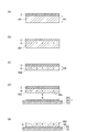
- FIG. 2 is a schematic cross-sectional view for explaining an embodiment of a method for manufacturing a semiconductor device, and FIGS. 2A, 2B, 2C, 2D, and 2E show each step. It is a schematic cross section which shows.
- FIG. 3 is a schematic cross-sectional view for explaining one embodiment of a method for manufacturing a semiconductor device, and FIGS. 3F, 3G, 3H, and 3I are schematic cross-sectional views showing each step. It is a figure.
- FIG. 4 is a schematic sectional view showing an embodiment of a semiconductor device.
- the numerical range indicated by using “to” indicates the range including the numerical values before and after “to” as the minimum value and the maximum value, respectively.
- the upper limit value or the lower limit value described in one numerical range may be replaced with the upper limit value or the lower limit value of another stepwise described numerical range.
- the upper limit value or the lower limit value of the numerical range may be replaced with the value shown in the examples.
- (meth)acrylate means acrylate or corresponding methacrylate.
- the “threading” is a modified form of the pressure-sensitive adhesive between the adherend and the pressure-sensitive adhesive, and when the pressure-sensitive adhesive is separated from the pressure-sensitive adhesive, It means a large deformation like a wall, and sometimes a wall, without being broken between and.
- the method for evaluating a photocurable pressure-sensitive adhesive used for the dicing/die-bonding integrated film is a photocurable pressure-sensitive adhesive sheet prepared from a photocurable pressure-sensitive adhesive, and the photocurable pressure-sensitive adhesive is prepared under the following tension and compression conditions.
- a tensile test is performed on the pressure-sensitive adhesive sheet, a graph of test force against displacement is created, and the first step of determining the area surrounded by the hysteresis curve as loss work from the obtained hysteresis curve, the base layer, and the light
- a second step of forming a cured product of the photocurable pressure-sensitive adhesive layer and measuring the peeling force when the cured product of the photocurable pressure-sensitive adhesive layer is peeled from the base material layer under the following peeling conditions And a third step of judging the quality of the photocurable pressure-sensitive adhesive based on the lost work and the peeling force.
- a photocurable pressure-sensitive adhesive that is cured by irradiation with ultraviolet rays can be an evaluation target.
- a photocurable pressure-sensitive adhesive to be evaluated a (meth)acrylic copolymer having a reactive functional group, a photopolymerization initiator, and two or more functional groups capable of reacting with the reactive functional group are provided.
- a photocurable pressure-sensitive adhesive containing a crosslinking agent will be described.
- the (meth)acrylic copolymer having a reactive functional group is, for example, one or more types of (meth)acrylate monomer (a1) or (meth)acrylic acid, and one type having a reactive functional group. Alternatively, it can be obtained by copolymerizing two or more kinds of polymerizable compounds (a2).
- Examples of the (meth)acrylate monomer (a1) include linear or branched alkyl (meth)acrylate, alicyclic (meth)acrylate, aromatic (meth)acrylate, alkoxyalkyl (meth)acrylate, and alkoxy (poly). It may be at least one selected from the group consisting of alkylene glycol (meth)acrylate, alkoxyalkoxyalkyl (meth)acrylate, and dialkylaminoalkyl (meth)acrylate.
- linear or branched alkyl (meth)acrylate examples include methyl (meth)acrylate, ethyl (meth)acrylate, n-propyl (meth)acrylate, n-butyl (meth)acrylate, isobutyl (meth)acrylate, t- Examples thereof include butyl (meth)acrylate, ethylhexyl (meth)acrylate, stearyl (meth)acrylate, lauryl (meth)acrylate, and tridecyl (meth)acrylate.
- alicyclic (meth)acrylate examples include cyclohexyl (meth)acrylate, isobornyl (meth)acrylate, dicyclopentanyl (meth)acrylate and the like.
- aromatic (meth)acrylates examples include phenoxyethyl (meth)acrylate.
- alkoxyalkyl (meth)acrylate examples include ethoxyethyl (meth)acrylate and butoxyethyl (meth)acrylate.
- alkoxy(poly)alkylene glycol(meth)acrylate examples include methoxydiethylene glycol(meth)acrylate, ethoxydiethylene glycol(meth)acrylate, methoxytriethylene glycol(meth)acrylate, butoxytriethylene glycol(meth)acrylate, methoxydipropylene. Examples thereof include glycol (meth)acrylate.
- alkoxyalkoxyalkyl (meth)acrylates examples include 2-methoxyethoxyethyl (meth)acrylate and 2-ethoxyethoxyethyl (meth)acrylate.
- dialkylaminoalkyl (meth)acrylate examples include N,N-dimethylaminoethyl (meth)acrylate and N,N-diethylaminoethyl (meth)acrylate.
- the polymerizable compound (a2) may have at least one reactive functional group selected from the group consisting of a hydroxy group and an epoxy group. Since the hydroxy group and the epoxy group have good reactivity with the compound (b) having an isocyanate group or the like, they can be preferably used.
- the polymerizable compound (a2) preferably has a hydroxy group.
- Examples of the polymerizable compound (a2) having a hydroxy group as a reactive functional group include hydroxyalkyl such as 2-hydroxyethyl (meth)acrylate, 2-hydroxybutyl (meth)acrylate and 2-hydroxypropyl (meth)acrylate. (Meth)acrylate etc. are mentioned.
- Examples of the polymerizable compound (a2) having an epoxy group as a reactive functional group include (meth)acrylate having an epoxy group such as glycidyl (meth)acrylate and 3,4-epoxycyclohexyl (meth)acrylate. ..
- the (meth)acrylic copolymer may contain (meth)acrylic acid as a monomer unit. Further, in addition to the (meth)acrylate monomer (a1) and the polymerizable compound (a2), another polymerizable compound may be contained as a monomer unit. Examples of other polymerizable compounds include aromatic vinyl compounds such as styrene and vinyltoluene.
- the (meth)acrylic copolymer having a reactive functional group may further have a chain-polymerizable functional group. That is, it may have a main chain made of a (meth)acrylic copolymer having a reactive functional group and a side chain containing a polymerizable double bond and bonded to the main chain.
- the side chain containing the polymerizable double bond may be a (meth)acryloyl group, but is not limited thereto.
- a (meth)acrylic copolymer having a chain-polymerizable functional group has a functional group that reacts with a reactive functional group of a (meth)acrylic copolymer having a reactive functional group and a chain-polymerizable functional group. It can be obtained by reacting one or more compounds (b) with each other to introduce a chain-polymerizable functional group into the side chain of the (meth)acrylic copolymer.
- Examples of the functional group that reacts with a reactive functional group include an isocyanate group and the like.
- compound (b) having an isocyanate group examples include 2-methacryloxyethyl isocyanate (for example, Showa Denko KK, trade name “Karenzu MOI”).
- the content of the compound (b) may be 0.3 to 1.5 mmol/g based on the (meth)acrylic copolymer having a reactive functional group.
- the acid value of the (meth)acrylic copolymer having a reactive functional group may be, for example, 1 to 150 mgKOH/g.
- the hydroxyl value of the (meth)acrylic copolymer having a reactive functional group may be, for example, 1 to 150 mgKOH/g.
- the acid value and the hydroxyl value are measured according to JIS K0070.
- the weight average molecular weight (Mw) of the (meth)acrylic copolymer having a reactive functional group may be 100,000 to 1,000,000, 200,000 to 600,000, or 250,000 to 400,000.
- the weight average molecular weight is a polystyrene conversion value using a calibration curve based on standard polystyrene by gel permeation chromatography (GPC).
- the photopolymerization initiator is not particularly limited as long as it initiates polymerization by irradiation with ultraviolet rays, and examples thereof include a photoradical polymerization initiator.
- the photoradical polymerization initiator include benzoin ketals such as 2,2-dimethoxy-1,2-diphenylethane-1-one; ⁇ -hydroxyketones such as 1-hydroxycyclohexylphenyl ketone; 2-benzyl-2- ⁇ -aminoketones such as dimethylamino-1-(4-morpholinophenyl)-butan-1-one; oximes such as 1-[4-(phenylthio)phenyl]-1,2-octadione-2-(benzoyl)oxime Ester; phosphine oxide such as bis(2,4,6-trimethylbenzoyl)phenylphosphine oxide; 2,4,5-triarylimidazole diamine such as 2-(o-chloroph
- the content of the photopolymerization initiator is 0.1 to 20 parts by mass, 0.3 to 10 parts by mass, or 0.5 to 3 parts by mass with respect to 100 parts by mass of the (meth)acrylic copolymer. Good.
- the cross-linking agent is not particularly limited as long as it is a compound having two or more functional groups capable of reacting with the reactive functional group (epoxy group, hydroxy group, etc.) of the (meth)acrylic copolymer having a reactive functional group.
- the bond formed by the reaction between the cross-linking agent and the (meth)acrylic copolymer having a reactive functional group include an ester bond, an ether bond, an amide bond, an imide bond, a urethane bond, and a urea bond. ..
- cross-linking agent examples include compounds having two or more isocyanate groups in one molecule. When such a compound is used, it easily reacts with the reactive functional group of the (meth)acrylic copolymer, so that the tackiness and stringiness tend to be easily controlled.
- Examples of the compound having two or more isocyanate groups in one molecule include 2,4-tolylene diisocyanate, 2,6-tolylene diisocyanate, 1,3-xylylene diisocyanate, 1,4-xylene diisocyanate and diphenylmethane- 4,4'-diisocyanate, diphenylmethane-2,4'-diisocyanate, 3-methyldiphenylmethane diisocyanate, hexamethylene diisocyanate, isophorone diisocyanate, dicyclohexylmethane-4,4'-diisocyanate, dicyclohexylmethane-2,4'-diisocyanate, lysine Examples thereof include isocyanate compounds such as isocyanate.
- Specific examples of the compound having two or more isocyanate groups in one molecule include polyfunctional isocyanate (manufactured by Nippon Polyurethane Industry Co., Ltd., trade name “Coronate L”).
- the cross-linking agent may be a reaction product of the above-mentioned isocyanate compound and a polyhydric alcohol having two or more hydroxy groups in one molecule (isocyanate group-containing oligomer).
- examples of the polyhydric alcohol having two or more hydroxy groups in one molecule include ethylene glycol, propylene glycol, butylene glycol, 1,6-hexanediol, 1,8-octanediol, 1,9-nonanediol, and 1 , 10-decanediol, 1,11-undecanediol, 1,12-dodecanediol, glycerin, pentaerythritol, dipentaerythritol, 1,4-cyclohexanediol, 1,3-cyclohexanediol and the like.
- the crosslinking agent is a reaction product (isocyanate group-containing oligomer) of a polyfunctional isocyanate having two or more isocyanate groups in one molecule and a polyhydric alcohol having three or more hydroxy groups in one molecule. May be.
- isocyanate group-containing oligomer As a crosslinking agent, the photocurable pressure-sensitive adhesive layer 20 tends to form a denser crosslinked structure.
- the content of the cross-linking agent may be, for example, 3 to 30 parts by mass, 4 to 15 parts by mass, or 5 to 10 parts by mass based on the total mass of the (meth)acrylic copolymer.
- FIG. 1 is a schematic cross-sectional view showing an embodiment of an integrated dicing/die bonding film.
- the dicing/die-bonding integrated film 1 includes a base material layer 10, a photo-curable pressure-sensitive adhesive layer 20 made of a photo-curable pressure-sensitive adhesive, and an adhesive layer 30 laminated in this order.
- the base material layer 10 may be a known polymer sheet or film, and is not particularly limited as long as it is made of a material that can be expanded in the die bonding step.
- a material include crystalline polypropylene, amorphous polypropylene, high-density polyethylene, medium-density polyethylene, low-density polyethylene, ultra-low-density polyethylene, low-density linear polyethylene, polybutene, polymethylpentene, and other polyolefins; Ethylene-vinyl acetate copolymer; ionomer resin; ethylene-(meth)acrylic acid copolymer; ethylene-(meth)acrylic acid ester (random, alternating) copolymer; ethylene-propylene copolymer; ethylene-butene copolymer Polymers; ethylene-hexene copolymers; polyurethanes; polyesters such as polyethylene terephthalate and polyethylene na
- the base material layer 10 is made of polyethylene, polypropylene, polyethylene-polypropylene random copolymer, and polyethylene-from the viewpoint of properties such as Young's modulus, stress relaxation property, melting point, price, recycling of waste materials after use, and the like. It may have a surface containing at least one material selected from polypropylene block copolymers as a main component, and the surface is in contact with the photocurable pressure-sensitive adhesive layer 20.
- the base material layer 10 may be a single layer or a multilayer including two or more layers made of different materials.
- the base material layer 10 may be subjected to surface roughening treatment such as corona discharge treatment or mat treatment, if necessary, from the viewpoint of controlling the adhesion with the photo-curable pressure-sensitive adhesive layer 20 described later.
- the thickness of the base material layer 10 may be, for example, 70 to 120 ⁇ m or 80 to 100 ⁇ m. When the thickness of the base material layer 10 is 70 ⁇ m or more, damage due to expansion tends to be more suppressed. When the thickness of the base material layer 10 is 120 ⁇ m or less, the stress in the pickup easily reaches the adhesive layer, and the pickup property tends to be more excellent.
- the photocurable pressure-sensitive adhesive layer 20 is a layer made of the above-mentioned photocurable pressure-sensitive adhesive.
- the photocurable pressure-sensitive adhesive layer 20 is formed on the base material layer 10.
- a varnish for forming a photocurable pressure sensitive adhesive layer is prepared, and the varnish is applied to the base material layer 10 to perform photocuring.
- a varnish is applied on a release-treated film to form a photo-curable pressure-sensitive adhesive layer 20, and the obtained photo-curable pressure-sensitive adhesive layer 20 is used as a substrate.
- the method of transferring to the layer 10 is mentioned.
- the varnish for forming a photocurable pressure-sensitive adhesive layer comprises a (meth)acrylic copolymer having a reactive functional group, a photopolymerization initiator, and a crosslinking agent having two or more functional groups capable of reacting with the reactive functional group and an organic solvent.
- a (meth)acrylic copolymer having a reactive functional group, a photopolymerization initiator, and a cross-linking agent having two or more functional groups capable of reacting with the reactive functional group can be used. May be volatilized by.
- organic solvents examples include aromatic hydrocarbons such as toluene and xylene; cyclic ethers such as tetrahydrofuran and 1,4-dioxane; alcohols such as methanol, ethanol, ethylene glycol and propylene glycol; acetone, methyl ethyl ketone and methyl.
- Ketones such as isobutyl ketone and cyclohexanone; esters such as methyl acetate, ethyl acetate and ⁇ -butyrolactone; carbonic acid esters such as ethylene carbonate and propylene carbonate; ethylene glycol monomethyl ether, ethylene glycol dimethyl ether, propylene glycol monomethyl ether, propylene glycol monoethyl ether , Polyhydric alcohol alkyl ethers such as propylene glycol dimethyl ether; polyhydric alcohol alkyl ether acetates such as ethylene glycol monomethyl ether acetate and ethylene glycol monoethyl ether acetate; N,N-dimethylformamide, N,N-dimethylacetamide, N-methyl Examples include amides such as 2-pyrrolidone. These may be used alone or in combination of two or more.
- the solid content concentration of the varnish may be 10 to 60% by weight, based on the total weight of the varnish.
- the thickness of the photocurable pressure-sensitive adhesive layer 20 may be, for example, 1 to 200 ⁇ m, 5 to 50 ⁇ m, or 10 to 20 ⁇ m.
- the adhesive layer 30 is a layer made of an adhesive.
- the adhesive is not particularly limited as long as it is an adhesive used in the field of die bonding film.
- an adhesive containing an epoxy resin, an epoxy resin curing agent, and a (meth)acrylic copolymer having an epoxy group will be described.
- the adhesive layer 30 made of such an adhesive it is possible to provide excellent adhesiveness between the chips and the substrate and between the chips, and to impart electrode embedding properties, wire embedding properties, and the like. In addition, it becomes possible to bond at low temperature in the die bonding process.
- epoxy resin examples include bisphenol A type epoxy resin, bisphenol F type epoxy resin, bisphenol S type epoxy resin, phenol novolac type epoxy resin, cresol novolac type epoxy resin, bisphenol A novolac type epoxy resin, bisphenol F novolac type epoxy resin.
- the epoxy resin curing agent may be, for example, a phenolic resin.
- the phenol resin can be used without particular limitation as long as it has a phenolic hydroxyl group in the molecule.
- examples of the phenolic resin include phenols such as phenol, cresol, resorcin, catechol, bisphenol A, bisphenol F, phenylphenol and aminophenol, and/or naphthols such as ⁇ -naphthol, ⁇ -naphthol and dihydroxynaphthalene, and formaldehyde.
- a novolak type phenolic resin obtained by condensation or co-condensation with a compound having an aldehyde group such as, for example, allylated bisphenol A, allylated bisphenol F, allylated naphthalene diol, phenol novolac, phenols and the like, and Examples thereof include phenol aralkyl resin and naphthol aralkyl resin synthesized from naphthols and dimethoxyparaxylene or bis(methoxymethyl)biphenyl. These may be used alone or in combination of two or more.
- the (meth)acrylic copolymer having an epoxy group may be a copolymer prepared by adjusting glycidyl (meth)acrylate as a raw material in an amount of 0.5 to 6% by mass based on the resulting copolymer. .. When the amount is 0.5% by mass or more, high adhesive strength tends to be easily obtained, and when the amount is 6% by mass or less, gelation tends to be suppressed.
- the balance of glycidyl (meth)acrylate may be a mixture of alkyl (meth)acrylate having an alkyl group having 1 to 8 carbon atoms such as methyl (meth)acrylate and styrene and acrylonitrile.
- the alkyl (meth)acrylate may include ethyl (meth)acrylate and/or butyl (meth)acrylate.
- the mixing ratio of each component can be adjusted in consideration of the Tg (glass transition point) of the obtained (meth)acrylic copolymer having an epoxy group.
- Tg glass transition point
- the upper limit of Tg of the (meth)acrylic copolymer having an epoxy group may be, for example, 30°C.
- the weight average molecular weight of the (meth)acrylic copolymer having an epoxy group may be 100,000 or more, and may be 300,000 to 3,000,000 or 500,000 to 2,000,000. When the weight average molecular weight is 3,000,000 or less, deterioration of the filling property between the semiconductor chip and the supporting substrate tends to be controlled.
- the weight average molecular weight is a polystyrene conversion value using a calibration curve based on standard polystyrene by gel permeation chromatography (GPC).
- the adhesive may further contain a curing accelerator such as a tertiary amine, imidazoles, or quaternary ammonium salts, if necessary.
- a curing accelerator such as a tertiary amine, imidazoles, or quaternary ammonium salts, if necessary.
- the curing accelerator include 2-methylimidazole, 2-ethyl-4-methylimidazole, 1-cyanoethyl-2-phenylimidazole, 1-cyanoethyl-2-phenylimidazolium trimellitate. These may be used alone or in combination of two or more.
- the adhesive may further contain an inorganic filler, if necessary.
- an inorganic filler for example, aluminum hydroxide, magnesium hydroxide, calcium carbonate, magnesium carbonate, calcium silicate, magnesium silicate, calcium oxide, magnesium oxide, aluminum oxide, aluminum nitride, aluminum borate whiskers, boron nitride, crystalline Examples thereof include silica and amorphous silica. These may be used alone or in combination of two or more.
- the adhesive layer 30 is formed on the photocurable pressure-sensitive adhesive layer 20.
- an adhesive layer-forming varnish is prepared, and the varnish is applied on a release-treated film to form an adhesive.
- a method of forming the layer 30 and transferring the obtained adhesive layer 30 to the photocurable pressure-sensitive adhesive layer 20 can be mentioned.
- the adhesive layer-forming varnish contains an epoxy resin, an epoxy resin curing agent, a (meth)acrylic copolymer having an epoxy group, and an organic solvent.
- the organic solvent may be the same as the organic solvent used in the varnish for forming a photocurable pressure-sensitive adhesive layer.
- the thickness of the adhesive layer 30 may be, for example, 1 to 300 ⁇ m, 5 to 150 ⁇ m, or 10 to 100 ⁇ m.
- the lost work may be affected by the interaction (for example, stringing phenomenon) at the interface between the photocurable pressure-sensitive adhesive layer and the adherend (adhesive layer). Therefore, as one of the factors influencing the lost work, the type and content of the crosslinking agent can be mentioned. For example, when the content of the cross-linking agent is decreased, the loss work tends to increase, and when the content of the cross-linking agent increases, the loss work tends to decrease. Therefore, the loss work can be controlled by adjusting the type and content of the crosslinking agent. Further, as other influential factors of the lost work, there are coating conditions, for example.
- a photocurable pressure sensitive adhesive sheet made of a photocurable pressure sensitive adhesive is prepared.
- the photocurable adhesive sheet is made of a photocurable adhesive.
- the photo-curable pressure-sensitive adhesive sheet is prepared, for example, by preparing the above-mentioned photo-curable pressure-sensitive adhesive layer-forming varnish, applying the varnish on a polyethylene terephthalate (PET) film subjected to a mold release treatment, and applying the varnish It can be obtained by removing volatile components and forming a photocurable pressure-sensitive adhesive layer.
- the photocurable pressure-sensitive adhesive sheet may have a polyethylene terephthalate (PET) film disposed as a protective film on the photocurable pressure-sensitive adhesive layer.
- the size of the photocurable pressure-sensitive adhesive sheet is not particularly limited as long as the chuck distance can be secured at 40 mm in the tensile test described later.
- the thickness of the photocurable pressure-sensitive adhesive sheet can be set to, for example, 10 ⁇ m.
- a tensile test is performed on the photocurable pressure-sensitive adhesive sheet under the following tensile and compression conditions.
- a graph of the test force against the displacement in the tensile test is created, and the area surrounded by the hysteresis curve is obtained from the obtained hysteresis curve as loss work.
- any evaluation processing analysis software may be used.
- a dicing/die-bonding integrated film for evaluation in which a base material layer, a photo-curable pressure-sensitive adhesive layer made of a photo-curable pressure-sensitive adhesive to be evaluated, and an adhesive layer are laminated in this order is prepared. ..
- the types of the base material layer, the photo-curable pressure-sensitive adhesive layer, and the adhesive layer are not particularly limited, and an arbitrarily selected dicing/die-bonding integrated film should be used.
- the thickness of the photo-curable pressure-sensitive adhesive composed of the photo-curable pressure-sensitive adhesive that is the object of evaluation can be set to 10 ⁇ m, for example.
- the thickness of the adhesive layer may be 10 ⁇ m, for example.
- the ultraviolet light source can be appropriately selected depending on the type of photopolymerization initiator used.
- the light source of ultraviolet light is not particularly limited, but may be one kind selected from the group consisting of a low pressure mercury lamp, a far ultraviolet lamp, an excimer ultraviolet lamp, a high pressure mercury lamp, and a metal halide lamp. Of these, the ultraviolet light source is preferably a high pressure mercury lamp having a central wavelength of 365 nm. Further, in the irradiation of ultraviolet rays, a cold mirror or the like may be used together in order to reduce the influence of heat emitted from the light source.
- the irradiation temperature under UV irradiation conditions may be 60°C or lower or 40°C or lower.
- a peel strength measuring device capable of adjusting the peel angle is used to attach an adhesive tape, a support tape, or the like to the adhesive layer. It is preferable to do this by pulling the tape.
- ⁇ Third step> the quality of the photocurable pressure-sensitive adhesive is judged based on the lost work and the peeling force.
- the values of the loss work and the peeling force, which are evaluation criteria, can be set to arbitrary values according to the thickness of the semiconductor wafer and the like.
- the third step may be a step of judging the quality of the photocurable pressure-sensitive adhesive depending on whether the lost work and the peeling force satisfy the following conditions (a) and (b).
- a dicing/die-bonding integrated film including a photo-curable pressure-sensitive adhesive layer made of a photo-curable pressure-sensitive adhesive that satisfies the following conditions (a) and (b) is a semiconductor wafer having a relatively small thickness (for example, 35 ⁇ m or less). Can be suitably used for the dicing process applied to (for example, stealth dicing).
- the loss work under the condition (a) may be 1.22 N ⁇ mm or more or 1.24 N ⁇ mm or more.
- the upper limit of the loss work under the condition (a) is not particularly limited, but may be 1.40 N ⁇ mm or less.
- the peeling force under the condition (b) may be 0.59 N/25 mm or less or 0.58 N/25 mm or less.
- the lower limit of the peeling force under the condition (b) is not particularly limited, but may be 0.54 N/25 mm or more.
- a method for producing a dicing/die-bonding integrated film is a photocurable adhesive comprising a photocurable adhesive determined to be good by the above-mentioned photocurable adhesive evaluation method on a base material layer. And a step of forming an adhesive layer on the photo-curable pressure-sensitive adhesive layer.
- the base material layer and the adhesive layer may be the same as those exemplified in the above-mentioned evaluation method for the photocurable pressure-sensitive adhesive.
- the method for forming the photocurable pressure-sensitive adhesive layer and the method for forming the adhesive layer may be the same as the method exemplified in the above-mentioned evaluation method for the photocurable pressure-sensitive adhesive.
- the dicing/die-bonding integrated film is a substrate layer, and a photo-curable pressure-sensitive adhesive layer made of a photo-curable pressure-sensitive adhesive that is determined to be good by the above-described photo-curable pressure-sensitive adhesive evaluation method, An adhesive layer is provided in this order.
- the base material layer and the adhesive layer may be the same as those exemplified in the above-mentioned evaluation method for the photocurable pressure-sensitive adhesive.
- FIGS. 2 and 3 are schematic cross-sectional views for explaining one embodiment of a method for manufacturing a semiconductor device.
- the semiconductor device manufacturing method according to the present embodiment includes a step (wafer laminating step) of attaching the adhesive layer 30 of the dicing/die-bonding integrated film 1 obtained by the above-described manufacturing method to the semiconductor wafer W2, and a semiconductor wafer W2.
- a step of dicing the adhesive layer 30 and the photocurable pressure-sensitive adhesive layer 20 into pieces (dicing step), a step of irradiating the photocurable pressure-sensitive adhesive layer 20 with ultraviolet rays (ultraviolet ray irradiation step), and a substrate
- a step of picking up a semiconductor element (semiconductor element 50 with an adhesive layer) to which the adhesive layer 30a is attached from the layer 10 (pickup step), and mounting the semiconductor element 50 with an adhesive layer on the semiconductor element via the adhesive layer 30a.
- a step of adhering to the supporting substrate 60 (semiconductor element adhering step).
- the dicing in the dicing process is not particularly limited, and examples thereof include blade dicing, laser dicing, stealth dicing and the like.
- the dicing may be stealth dicing.
- stealth dicing is mainly used as the dicing will be described in detail.
- the method for manufacturing a semiconductor device may include a modified layer forming step before the wafer laminating step.
- a semiconductor wafer W1 having a thickness H1 is prepared.
- the thickness H1 of the semiconductor wafer W1 forming the modified layer may exceed 35 ⁇ m.
- the protective film 2 is attached to one main surface of the semiconductor wafer W1 (see FIG. 2A).
- the surface to which the protective film 2 is attached is preferably the circuit surface of the semiconductor wafer W1.
- the protective film 2 may be a back grinding tape used for back surface grinding (back grinding) of a semiconductor wafer.
- the modified layer 4 is formed by irradiating the inside of the semiconductor wafer W1 with laser light (see FIG. 2B), and the side of the semiconductor wafer W1 opposite to the side where the protective film 2 is attached (back side).
- the semiconductor wafer W2 having the modified layer 4 is manufactured by performing back grinding (back surface grinding) and polishing (polishing) on the above (see FIG. 2C).
- the thickness H2 of the obtained semiconductor wafer W2 may be 35 ⁇ m or less.
- the adhesive layer 30 of the dicing/die bonding integrated film 1 is placed in a predetermined device.
- the dicing/die bonding integrated film 1 is attached to the main surface Ws of the semiconductor wafer W2 via the adhesive layer 30 (see FIG. 2D), and the protective film 2 of the semiconductor wafer W2 is peeled off ( 2(e)).
- the photocurable pressure-sensitive adhesive layer 20 is irradiated with ultraviolet rays to cure the photocurable pressure-sensitive adhesive in the photocurable pressure-sensitive adhesive layer 20, and the cured product of the photocurable pressure-sensitive adhesive layer (of the photocurable pressure-sensitive adhesive is A layer containing a cured product) is formed (see FIG. 3(g)).
- the adhesive force between the photocurable pressure-sensitive adhesive layer 20 and the adhesive layer 30 can be reduced.
- ultraviolet rays it is preferable to use ultraviolet rays having a wavelength of 200 to 400 nm.
- the ultraviolet irradiation conditions are preferably adjusted so that the illuminance is 30 to 240 mW/cm 2 and the irradiation amount is 200 to 500 mJ/cm 2 .
- the base material layer 10 is expanded to separate the diced semiconductor elements 50 with an adhesive layer from each other, while sucking the semiconductor element 50 with an adhesive layer pushed up by the needle 42 from the base material layer 10 side. It is sucked by the collet 44 and picked up from the cured product 20ac of the photocurable pressure-sensitive adhesive layer (see FIG. 3(h)).
- the semiconductor element 50 with the adhesive layer has the semiconductor element Wa and the adhesive layer 30a.
- the semiconductor element Wa is obtained by dividing the semiconductor wafer W2 by dicing
- the adhesive layer 30a is obtained by dividing the adhesive layer 30 by dicing.
- the cured product 20ac of the photocurable adhesive layer is obtained by dividing the cured product of the photocurable adhesive layer by dicing.
- the cured product 20ac of the photocurable pressure-sensitive adhesive layer may remain on the base material layer 10 when the semiconductor element 50 with the adhesive layer is picked up. In the pickup process, it is not always necessary to expand, but the expandability can be further improved by expanding.
- the amount of thrust by the needle 42 can be set appropriately. Further, for example, two-stage or three-stage pickup may be performed from the viewpoint of ensuring a sufficient pickup property even for an extremely thin wafer.
- the semiconductor element 50 with the adhesive layer may be picked up by a method other than the method using the suction collet 44.
- the semiconductor element 50 with the adhesive layer is bonded to the semiconductor element mounting support substrate 60 via the adhesive layer 30a by thermocompression bonding (see FIG. 3(f)). ..
- a plurality of adhesive layer-equipped semiconductor elements 50 may be bonded to the semiconductor element mounting support substrate 60.
- FIG. 4 is a sectional view schematically showing an embodiment of a semiconductor device.
- the semiconductor device 100 shown in FIG. 4 includes the above steps, the step of electrically connecting the semiconductor element Wa and the semiconductor element mounting support substrate 60 by wire bonds 70, and the step of electrically connecting the semiconductor element Wa and the semiconductor element mounting support substrate 60 on the surface 60 a of the semiconductor element mounting support substrate 60. And a step of resin-sealing the semiconductor element Wa using the resin sealing material 80.
- Solder balls 90 may be formed on the surface of the semiconductor element mounting support substrate 60 opposite to the surface 60a for electrical connection with an external substrate (motherboard).
- reaction solution was transferred to a pressure vessel having a capacity of 2000 mL equipped with a three-one motor, a stirring blade, and a nitrogen introducing tube, and heated at 120° C. and 0.28 MPa for 6 hours, and then at room temperature (25° C., the same below). Cooled down. Next, 89 parts by mass of ethyl acetate was further added for dilution.
- the acid value and hydroxyl value of the (meth)acrylic copolymer in the (meth)acrylic copolymer solution were measured according to JIS K0070.
- the acid value was 10.2 mgKOH/g and the hydroxyl value was 80.0 mgKOH/g.
- the obtained acrylic resin was vacuum dried at 60° C. overnight, and the obtained solid content was subjected to elemental analysis by a fully automatic elemental analyzer varioEL manufactured by Elemental Co., Ltd.
- the content of methacryloxyethyl isocyanate was calculated.
- the content of 2-methacryloxyethyl isocyanate was 0.90 mmol/g.
- ⁇ Production Example 1 Preparation of photo-curable pressure-sensitive adhesive sheet A and dicing/die-bonding integrated film A> (Preparation of photocurable adhesive A) 100 parts by mass of the (meth)acrylic copolymer solution prepared above as a (meth)acrylic copolymer having a reactive functional group as a solid content, 1-hydroxycyclohexyl phenyl ketone as a photopolymerization initiator (Ciba Specialty Chemicals Co., Ltd.
- Irgacure 184 0.6 parts by mass of Irgacure 184) manufactured by the company and 0.3 parts by mass of bis(2,4,6-trimethylbenzoyl)-phenylphosphine oxide (Irgacure 819 manufactured by Ciba Specialty Chemicals Co., Ltd.) and polyfunctional as a crosslinking agent. 6.8 parts by mass of isocyanate (manufactured by Nippon Polyurethane Industry Co., Ltd., trade name "Coronate L", solid content 75%) were mixed. Ethyl acetate was added to this mixture so that the total solid content was 25% by mass, and the mixture was uniformly stirred for 10 minutes to obtain a varnish of the photocurable pressure-sensitive adhesive A.
- the thickness of the photocurable pressure sensitive adhesive layer (photocurable pressure sensitive adhesive sheet) after drying is Coating was performed using a coating machine so that the thickness was 10 ⁇ m. The coating was performed under the conditions of a speed of 3.0 m/min, a first drying oven temperature of 80°C, and a second drying oven temperature of 80°C.
- a photo-curable pressure-sensitive adhesive layer in which a PET film having a thickness of 38 ⁇ m is arranged on the obtained photo-curable pressure-sensitive adhesive layer (photo-curable pressure-sensitive adhesive sheet) and sandwiched between two PET films Sheet).
- the varnish of the photocurable pressure-sensitive adhesive A described above is dried on one surface of a polyethylene terephthalate (PET) film having a width of 350 mm, a length of 400 mm and a thickness of 38 ⁇ m, and the thickness of the photocurable pressure-sensitive adhesive layer after drying is 10 ⁇ m.
- the coating was performed while adjusting the gap so that the photocurable pressure-sensitive adhesive layer-forming varnish was heated and dried at 80 to 100° C. for 3 minutes.
- a polyolefin film base material layer, thickness: 90 ⁇ m
- the dicing film provided with the photocurable adhesive layer was obtained.
- the cross-linking treatment was performed while confirming the progress of curing by using FT-IR spectrum.
- NUCA-189 manufactured by Nippon Unicar Co., Ltd., trade name, ⁇ - 1.7 parts by mass of mercaptopropyltrimethoxysilane
- NUCA-1160 manufactured by Nippon Unicar Co., Ltd., trade name, ⁇ -ureidopropyltriethoxysilane
- Aerosil R972 as a filler (silica surface is dimethyldi).
- HTR-860P-3 manufactured by Nagase Chemtex Co., Ltd., trade name, acrylic rubber containing a weight-average molecular weight of 800,000, glycidyl acrylate or 3% by mass of glycidyl methacrylate
- an adhesive layer by adding 0.5 parts by mass of Cureazole 2PZ-CN (manufactured by Shikoku Kasei Co., Ltd., trade name, 1-cyanoethyl-2-phenylimidazole) as a curing accelerator, stirring and mixing, and degassing under vacuum. I got a varnish.
- the obtained adhesive layer-forming varnish was applied on a release-treated polyethylene terephthalate (PET) film having a thickness of 38 ⁇ m and dried by heating at 140° C. for 5 minutes to form a B-stage coating film having a thickness of 10 ⁇ m. Then, a die bonding film having an adhesive layer was formed.
- PET polyethylene terephthalate
- the die bonding film produced above was cut into a size that was easy to handle together with the PET film.
- a dicing/die-bonding integrated film A was obtained by sticking the photocurable pressure-sensitive adhesive layer of the dicing film from which the PET film was peeled off to the adhesive layer of the cut die bonding film.
- the lamination was performed using a laminating machine in a clean room (23° C. temperature, 50% humidity-free room).
- ⁇ Production Example 2 Preparation of photocurable pressure-sensitive adhesive sheet B and dicing/die-bonding integrated film B> A photocurable pressure-sensitive adhesive sheet B and a dicing/die-bonding integrated film B were obtained in the same manner as in Production Example 1, except that the content of the crosslinking agent was changed from 6.8 parts by mass to 7.2 parts by mass. ..
- ⁇ Preparation of evaluation sample> (Formation of modified layer) A back grinding tape was attached to one surface of a semiconductor wafer (silicon wafer (thickness 750 ⁇ m, outer diameter 12 inches)) to obtain a semiconductor wafer with a back grinding tape. The surface of the semiconductor wafer opposite to the side to which the back grinding tape was attached was irradiated with laser light to form a modified layer inside the semiconductor wafer.
- the laser irradiation conditions are as follows.
- Laser oscillator model Semiconductor laser pumped Q-switch solid-state laser Wavelength: 1342 nm Oscillation form: pulse Frequency: 90 kHz Output: 1.7W Moving speed of semiconductor wafer mounting table: 700 mm/sec
- the PET film of the dicing/die bonding integrated film was peeled off from the surface of the semiconductor wafer opposite to the side to which the back grinding tape was stuck, and the adhesive layer was stuck.
- the dicing/die-bonding integrated film-equipped semiconductor wafer having the modified layer was fixed to an expanding device.
- the dicing film was expanded under the following conditions to separate the semiconductor wafer, the adhesive layer, and the photocurable pressure-sensitive adhesive layer into individual pieces.
- this individualized sample before irradiation with ultraviolet rays was used as an evaluation sample.
- Cool expanding conditions Temperature: -15°C, Height: 9 mm, Cooling time: 90 seconds, Speed: 300 mm/sec, Standby time: 0 seconds
- Heat shrink (heat expand) conditions Temperature: 220°C, height: 7 mm, holding time: 15 seconds, speed: 30 mm/sec, heater speed: 7°C/sec
- UV irradiation The center wavelength of 365nm ultraviolet irradiation with a light-curable pressure-sensitive adhesive layer of the singulated semiconductor wafer irradiation intensity 70 mW / cm 2 and cumulative light quantity 150 mJ / cm 2, to form a cured product of the photocurable pressure-sensitive adhesive layer ..
- the individualized sample after irradiation with ultraviolet rays was used as an evaluation sample.
- the dicing/die-bonding integrated films A to C of Production Examples 1 to 3 have a loss work of 1.21 N ⁇ mm or more and a peeling force of 0.60 N/25 mm or less, Both the condition (a) and the condition (b) were satisfied.
- the dicing/die-bonding integrated films A to C of Production Examples 1 to 3 were excellent in chip floating and pickup property.
- the dicing/die bonding integrated films DF of Production Examples 4 to 6 which did not satisfy both the condition (a) and the condition (b) did not satisfy both the chip floating property and the pickup property. did.
- SYMBOLS 1 Dicing/die-bonding integrated film, 2... Protective film, 4... Modification layer, 10... Base material layer, 20... Photocurable adhesive layer, 20ac... Cured product of photocurable adhesive layer, 30, 30a... Adhesive layer, 42... Needle, 44... Suction collet, 50... Adhesive layer-equipped semiconductor element, 60... Support substrate for mounting semiconductor element, 70... Wire bond, 80... Resin encapsulant, 90... Solder ball, W1, W2... Semiconductor wafer, H1... Thickness of semiconductor wafer W1, H2... Thickness of semiconductor wafer W2, 100... Semiconductor device.
Landscapes
- Chemical & Material Sciences (AREA)
- Organic Chemistry (AREA)
- Physics & Mathematics (AREA)
- Engineering & Computer Science (AREA)
- Optics & Photonics (AREA)
- General Physics & Mathematics (AREA)
- Biochemistry (AREA)
- Pathology (AREA)
- Immunology (AREA)
- General Health & Medical Sciences (AREA)
- Health & Medical Sciences (AREA)
- Life Sciences & Earth Sciences (AREA)
- Analytical Chemistry (AREA)
- Mechanical Engineering (AREA)
- Oil, Petroleum & Natural Gas (AREA)
- Chemical Kinetics & Catalysis (AREA)
- Plasma & Fusion (AREA)
- General Chemical & Material Sciences (AREA)
- Adhesives Or Adhesive Processes (AREA)
- Dicing (AREA)
- Adhesive Tapes (AREA)
Abstract
Description
(引張圧縮条件)
温度:25±5℃
湿度:55±10%
チャック間距離:40mm
引張条件:試験力が0.5Nになるまで500mm/分で引張
圧縮条件:変位が0mmになるまで500mm/分で圧縮
(照射条件)
照射強度:70mW/cm2
積算光量:150mJ/cm2
(剥離条件)
温度:25±5℃
湿度:55±10%
剥離角度:30°
剥離速度:600mm/分
条件(a):損失仕事が1.21N・mm以上である。
条件(b):剥離力が0.60N/25mm以下である。
一実施形態に係るダイシング・ダイボンディング一体型フィルムに用いられる光硬化性粘着剤の評価方法は、光硬化性粘着剤からなる光硬化性粘着剤シートを準備し、下記引張圧縮条件で光硬化性粘着剤シートに対して引張試験を実施して、変位に対する試験力のグラフを作成し、得られるヒステリシス曲線からヒステリシス曲線で囲われる面積を損失仕事として求める第1の工程と、基材層、光硬化性粘着剤からなる光硬化性粘着剤層、及び接着剤層がこの順に積層されたダイシング・ダイボンディング一体型フィルムを準備し、光硬化性粘着剤層に対して下記照射条件で紫外線を照射して、光硬化性粘着剤層の硬化物を形成し、下記剥離条件で基材層から光硬化性粘着剤層の硬化物を剥離させたときの剥離力を測定する第2の工程と、損失仕事及び剥離力に基づいて、光硬化性粘着剤の良否を判
定する第3の工程とを備える。
本実施形態に係る光硬化性粘着剤の評価方法では、紫外線の照射によって硬化する光硬化性粘着剤が評価対象となり得る。以下、評価対象となる光硬化性粘着剤の一例として、反応性官能基を有する(メタ)アクリル共重合体と、光重合開始剤と、反応性官能基と反応可能な官能基を2以上有する架橋剤とを含有する光硬化性粘着剤を説明する。
反応性官能基を有する(メタ)アクリル共重合体は、例えば、1種又は2種以上の(メタ)アクリレート単量体(a1)又は(メタ)アクリル酸と、反応性官能基を有する1種又は2種以上の重合性化合物(a2)とを共重合することによって得ることができる。
光重合開始剤としては、紫外線の照射によって重合を開始させるものであれば特に制限されず、例えば、光ラジカル重合開始剤等が挙げられる。光ラジカル重合開始剤としては、例えば、2,2-ジメトキシ-1,2-ジフェニルエタン-1-オン等のベンゾインケタール;1-ヒドロキシシクロヘキシルフェニルケトン等のα-ヒドロキシケトン;2-ベンジル-2-ジメチルアミノ-1-(4-モルフォリノフェニル)-ブタン-1-オン等のα-アミノケトン;1-[4-(フェニルチオ)フェニル]-1,2-オクタジオン-2-(ベンゾイル)オキシム等のオキシムエステル;ビス(2,4,6-トリメチルベンゾイル)フェニルホスフィンオキシド等のホスフィンオキシド;2-(o-クロロフェニル)-4,5-ジフェニルイミダゾール二量体等の2,4,5-トリアリールイミダゾール二量体;ベンゾフェノン、N,N,N’,N’-テトラメチル-4,4’-ジアミノベンゾフェノン等のベンゾフェノン化合物;2-エチルアントラキノン等のキノン化合物;ベンゾインメチルエーテル等のベンゾインエーテル;ベンゾイン等のベンゾイン化合物;ベンジルジメチルケタール等のベンジル化合物;9-フェニルアクリジン等のアクリジン化合物:N-フェニルグリシン、クマリンなどが挙げられる。これらは1種を単独で又は2種以上を組み合わせて用いてもよく、適切な増感剤と組み合わせて用いてもよい。
架橋剤は、反応性官能基を有する(メタ)アクリル共重合体の反応性官能基(エポキシ基、ヒドロキシ基等)と反応可能な官能基を2以上有する化合物であれば特に制限されない。架橋剤と反応性官能基を有する(メタ)アクリル共重合体との反応によって形成される結合としては、例えば、エステル結合、エーテル結合、アミド結合、イミド結合、ウレタン結合、ウレア結合等が挙げられる。
図1は、ダイシング・ダイボンディング一体型フィルムの一実施形態を示す模式断面図である。ダイシング・ダイボンディング一体型フィルム1は、基材層10、光硬化性粘着剤からなる光硬化性粘着剤層20、及び接着剤層30がこの順に積層されている。
基材層10は、既知のポリマーシート又はフィルムを用いることができ、ダイボンディング工程においてエキスパンドすることが可能な材料で構成されているのであれば、特に制限されない。このような材料としては、例えば、結晶性ポリプロピレン、非晶性ポリプロピレン、高密度ポリエチレン、中密度ポリエチレン、低密度ポリエチレン、超低密度ポリエチレン、低密度直鎖ポリエチレン、ポリブテン、ポリメチルペンテン等のポリオレフィン;エチレン-酢酸ビニル共重合体;アイオノマー樹脂;エチレン-(メタ)アクリル酸共重合体;エチレン-(メタ)アクリル酸エステル(ランダム、交互)共重合体;エチレン-プロピレン共重合体;エチレン-ブテン共重合体;エチレン-ヘキセン共重合体;ポリウレタン;ポリエチレンテレフタレート、ポリエチレンナフタレート等のポリエステル;ポリカーボネート;ポリイミド;ポリエーテルエーテルケトン;ポリイミド;ポリエーテルイミド;ポリアミド;全芳香族ポリアミド;ポリフェニルスルフイド;アラミド(紙);ガラス;ガラスクロス;フッ素樹脂;ポリ塩化ビニル;ポリ塩化ビニリデン;セルロース系樹脂;シリコーン樹脂などが挙げられる。これらの材料は、可塑剤、シリカ、アンチブロッキング材、スリップ剤、帯電防止剤等と混合した材料であってもよい。
光硬化性粘着剤層20は、上述の光硬化性粘着剤からなる層である。光硬化性粘着剤層20は、基材層10上に形成されている。基材層10上に光硬化性粘着剤層20を形成する方法としては、例えば、光硬化性粘着剤層形成用ワニスを調製し、当該ワニスを基材層10に塗工して、光硬化性粘着剤層20を形成する方法、当該ワニスを離型処理されたフィルム上に塗工し、光硬化性粘着剤層20を形成して、得られた光硬化性粘着剤層20を基材層10に転写する方法が挙げられる。
接着剤層30は、接着剤からなる層である。接着剤は、ダイボンディングフィルムの分野で使用される接着剤であれば特に制限されない。以下、接着剤の一例として、エポキシ樹脂と、エポキシ樹脂硬化剤と、エポキシ基を有する(メタ)アクリル共重合体とを含有する接着剤を説明する。このような接着剤からなる接着剤層30によれば、チップと基板との間、チップとチップとの間の接着性に優れ、電極埋め込み性、ワイヤー埋め込み性等を付与することが可能であり、かつダイボンディング工程において、低温で接着することが可能となる。
損失仕事は、光硬化性粘着剤層と被着体(接着剤層)との界面での相互作用(例えば、糸曳き現象等)が影響し得る。そのため、損失仕事の影響因子の1つとしては、架橋剤の種類及び含有量が挙げられる。例えば、架橋剤の含有量を減少させると、損失仕事は大きくなり、架橋剤の含有量を増加させると、損失仕事は小さくなる傾向にある。したがって、架橋剤の種類及び含有量を調整することによって、損失仕事を制御し得る。また、その他の損失仕事の影響因子としては、例えば、塗工条件が挙げられる。
本工程では、まず、光硬化性粘着剤からなる光硬化性粘着剤シートを準備する。
温度:25±5℃
湿度:55±10%
チャック間距離:40mm
引張条件:試験力が0.5Nになるまで500mm/分で引張
圧縮条件:変位が0mmになるまで500mm/分で圧縮
本工程では、まず、基材層、評価対象である光硬化性粘着剤からなる光硬化性粘着剤層、及び接着剤層がこの順に積層された評価用ダイシング・ダイボンディング一体型フィルムを準備する。
照射強度:70mW/cm2
積算光量:150mJ/cm2
温度:25±5℃
湿度:55±10%
剥離角度:30°
剥離速度:600mm/分
本工程では、損失仕事及び剥離力に基づいて、光硬化性粘着剤の良否を判定する。評価基準である損失仕事及び剥離力の数値は、半導体ウエハの厚み等に合わせて任意の数値を設定することができる。
条件(b):剥離力が0.60N/25mm以下である。
一実施形態に係るダイシング・ダイボンディング一体型フィルムの製造方法は、基材層上に、上述の光硬化性粘着剤の評価方法で良と判定された光硬化性粘着剤からなる光硬化性粘着剤層を形成する工程と、光硬化性粘着剤層上に接着剤層を形成する工程とを備える。基材層及び接着剤層は、上述の光硬化性粘着剤の評価方法で例示したものと同様のものであってよい。光硬化性粘着剤層の形成方法及び接着剤層の形成方法も、上述の光硬化性粘着剤の評価方法で例示した方法と同様であってよい。
一実施形態に係るダイシング・ダイボンディング一体型フィルムは、基材層と、上述の光硬化性粘着剤の評価方法で良と判定された光硬化性粘着剤からなる光硬化性粘着剤層と、接着剤層とをこの順に備える。基材層及び接着剤層は、上述の光硬化性粘着剤の評価方法で例示したものと同様のものであってよい。
図2及び図3は、半導体装置の製造方法の一実施形態を説明するための模式断面図である。本実施形態に係る半導体装置の製造方法は、上述の製造方法によって得られるダイシング・ダイボンディング一体型フィルム1の接着剤層30を半導体ウエハW2に貼り付ける工程(ウエハラミネート工程)と、半導体ウエハW2、接着剤層30、及び光硬化性粘着剤層20を個片化する工程(ダイシング工程)と、光硬化性粘着剤層20に対して紫外線を照射する工程(紫外線照射工程)と、基材層10から接着剤層30aが付着した半導体素子(接着剤層付き半導体素子50)をピックアップする工程(ピックアップ工程)と、接着剤層30aを介して、接着剤層付き半導体素子50を半導体素子搭載用支持基板60に接着する工程(半導体素子接着工程)とを備える。
ダイシングがステルスダイシングを適用したものである場合、半導体装置の製造方法は、ウエハラミネート工程の前に改質層形成工程を備えていてよい。
次いで、ダイシング・ダイボンディング一体型フィルム1の接着剤層30を所定の装置に配置する。続いて、半導体ウエハW2の主面Wsに、接着剤層30を介してダイシング・ダイボンディング一体型フィルム1を貼り付け(図2(d)参照)、半導体ウエハW2の保護フィルム2を剥離する(図2(e)参照)。
次に、少なくとも半導体ウエハW2及び接着剤層30をダイシングによって個片化する(図3(f)参照)。ダイシングがステルスダイシングを適用したものである場合、ク-ルエキスパンド及びヒートシュリンクを行うことによって個片化することができる。
次に、光硬化性粘着剤層20に紫外線を照射することによって光硬化性粘着剤層20における光硬化性粘着剤を硬化させ、光硬化性粘着剤層の硬化物(光硬化性粘着剤の硬化物を含む層)を形成する(図3(g)参照)。これによって、光硬化性粘着剤層20と接着剤層30との間の粘着力を低下させることができる。紫外線照射においては、波長200~400nmの紫外線を用いることが好ましい。紫外線照射条件は、照度:30~240mW/cm2で照射量200~500mJ/cm2となるように調整することが好ましい。
次に、基材層10をエキスパンドすることによって、ダイシングされた接着剤層付き半導体素子50を互いに離間させつつ、基材層10側からニードル42で突き上げられた接着剤層付き半導体素子50を吸引コレット44で吸引して、光硬化性粘着剤層の硬化物20acからピックアップする(図3(h)参照)。なお、接着剤層付き半導体素子50は、半導体素子Waと接着剤層30aとを有する。半導体素子Waは半導体ウエハW2がダイシングによって分割されたものであり、接着剤層30aは接着剤層30がダイシングによって分割されたものである。光硬化性粘着剤層の硬化物20acは光硬化性粘着剤層の硬化物がダイシングによって分割されたものである。光硬化性粘着剤層の硬化物20acは接着剤層付き半導体素子50をピックアップする際に基材層10上に残存し得る。ピックアップ工程では、必ずしもエキスパンドする必要はないが、エキスパンドすることによってピックアップ性をより向上させることができる。
接着剤層付き半導体素子50をピックアップした後、接着剤層付き半導体素子50を、熱圧着によって、接着剤層30aを介して半導体素子搭載用支持基板60に接着する(図3(f)参照)。半導体素子搭載用支持基板60には、複数の接着剤層付き半導体素子50を接着してもよい。
((メタ)アクリル共重合体溶液の調製)
スリーワンモータ、撹拌翼、及び窒素導入管が備え付けられた容量2000mLのオートクレーブに、2-エチルヘキシルアクリレート(2EHA)79質量部、2-ヒドロキシエチルアクリレート(HEA)19質量部、及びメタクリル酸(MAA)2質量部を加え、さらに酢酸エチル127質量部及びアゾビスイソブチロニトリル0.04質量部を加えた。これを均一になるまで撹拌し、流量500ml/minで60分間バブリングを実施し、系中の溶存酸素を脱気した。次いで、1時間かけて80℃まで昇温し、80℃で維持したまま6時間重合させた。その後、スリーワンモータ、撹拌翼、及び窒素導入管が備え付けられた容量2000mLの加圧釜に反応溶液を移し、120℃、0.28MPa条件で6時間加温した後、室温(25℃、以下同様)まで冷却した。次に、酢酸エチルを89質量部さらに加えて希釈した。これに重合禁止剤としてジブチルヒドロキシトルエン0.005質量部及びウレタン化触媒としてジオクチルスズジラウレート0.011質量部を添加し、連鎖重合可能な官能基を有する化合物として2-メタクリロキシエチルイソシアネート(昭和電工株式会社製、商品名「カレンズMOI」)14質量部を加えて、70℃で12時間反応させ、室温まで冷却した。その後、不揮発分(固形分)含有量が35質量%となるように酢酸エチルを加えて、反応性官能基としてヒドロキシ基を有する(メタ)アクリル共重合体溶液を得た。
(光硬化性粘着剤Aの調製)
反応性官能基を有する(メタ)アクリル共重合体として上記で調製した(メタ)アクリル共重合体溶液を固形分として100質量部、光重合開始剤として1-ヒドロキシシクロヘキシルフェニルケトン(チバスペシャリティケミカルズ株式会社製、イルガキュア184)0.6質量部及びビス(2,4,6-トリメチルベンゾイル)-フェニルホスフィンオキシド(チバスペシャリティケミカルズ株式会社製、イルガキュア819)0.3質量部、並びに架橋剤として多官能イソシアネート(日本ポリウレタン工業株式会社製、商品名「コロネートL」、固形分75%)6.8質量部を混合した。この混合物に対して、固形分の総含有量が25質量%となるように酢酸エチルを加え、10分間均一に撹拌して、光硬化性粘着剤Aのワニスを得た。
上述の光硬化性粘着剤Aのワニスを、片面が離型処理された厚み20μmのポリエチレンテレフタレート(PET)フィルム上に乾燥後の光硬化性粘着剤層(光硬化性粘着剤シート)の厚みが10μmとなるように、塗工機を用いて塗工した。塗工は、速度3.0m/分、第一乾燥炉温度80℃、第二乾燥炉温度80℃の条件で行った。得られた光硬化性粘着剤層(光硬化性粘着剤シート)上に、厚み38μmのPETフィルムを配置し、2枚のPETフィルムに挟持された光硬化性粘着剤層(光硬化性粘着剤シート)を得た。
上述の光硬化性粘着剤Aのワニスを、片面が離型処理された幅350mm、長さ400mm、厚み38μmのポリエチレンテレフタレート(PET)フィルム上に乾燥後の光硬化性粘着剤層の厚みが10μmとなるように、ギャップを調整しながら塗工し、80~100℃で光硬化性粘着剤層形成用ワニスを3分間加熱乾燥した。その後、片面にコロナ放電処理が施されたポリオレフィン製フィルム(基材層、厚み:90μm)を貼り合わせ、40℃、72時間の条件で養生を行い、架橋処理を行うことによって、基材層と光硬化性粘着剤層とを備えるダイシングフィルムを得た。なお、架橋処理は、FT-IRスペクトルを用いて、養生の進行を確認しながら行った。
エポキシ樹脂としてYDCN-703(東都化成株式会社製、商品名、クレゾールノボラック型エポキシ樹脂、エポキシ当量210、分子量1200、軟化点80℃)55質量部、フェノール樹脂としてミレックスXLC-LL(三井化学株式会社製、商品名、水酸基当量175、吸水率1.8%、350℃における加熱質量減少率4%)45質量部、シランカップリング剤としてNUCA-189(日本ユニカー株式会社製、商品名、γ-メルカプトプロピルトリメトキシシラン)1.7質量部及びNUCA-1160(日本ユニカー株式会社製、商品名、γ-ウレイドプロピルトリエトキシシラン)3.2質量部、並びにフィラーとしてアエロジルR972(シリカ表面をジメチルジクロロシランで被覆し、400℃の反応器中で加水分解して、メチル基等の有機基によって表面修飾されたシリカフィラー、日本アエロジル株式会社製、商品名、平均粒径0.016μm)32質量部に、シクロヘキサノンを加えて撹拌混合し、さらにビーズミルを用いて90分混錬した。得られた混合物に対して、アクリルゴムとしてHTR-860P-3(ナガセケムテックス株式会社製、商品名、重量平均分子量80万、グリシジルアクリレート又はグリシジルメタクリレート3質量%を含むアクリルゴム)280質量部及び硬化促進剤としてキュアゾール2PZ-CN(四国化成株式会社製、商品名、1-シアノエチル-2-フェニルイミダゾール)0.5質量部加えて撹拌混合し、真空脱気することによって、接着剤層形成用ワニスを得た。得られた接着剤層形成用ワニスを厚み38μmの離型処理されたポリエチレンテレフタレート(PET)フィルム上に塗布し、140℃で5分間加熱乾燥して、厚みが10μmのBステージ状態の塗膜を形成し、接着剤層を備えるダイボンディングフィルムを作製した。
上記で作製したダイボンディングフィルムをPETフィルムごと取り扱いし易いサイズにカットした。カットしたダイボンディングフィルムの接着剤層に、PETフィルムを剥離したダイシングフィルムの光硬化性粘着剤層を貼り合わせることによって、ダイシング・ダイボンディング一体型フィルムAを得た。貼り合わせは、クリーンルーム(温度23℃、湿度50%の無塵室内)でラミネートマシンを用いて行った。
架橋剤の含有量を6.8質量部から7.2質量部に変更した以外は、製造例1と同様にして、光硬化性粘着剤シートB及びダイシング・ダイボンディング一体型フィルムBを得た。
架橋剤の含有量を6.8質量部から7.6質量部に変更した以外は、製造例1と同様にして、光硬化性粘着剤シートC及びダイシング・ダイボンディング一体型フィルムCを得た。
架橋剤の含有量を6.8質量部から4.0質量部に変更した以外は、製造例1と同様にして、光硬化性粘着剤シートD及びダイシング・ダイボンディング一体型フィルムDを得た。
架橋剤の含有量を6.8質量部から6.4質量部に変更した以外は、製造例1と同様にして、光硬化性粘着剤シートE及びダイシング・ダイボンディング一体型フィルムEを得た。
架橋剤の含有量を6.8質量部から8.0質量部に変更した以外は、製造例1と同様にして、光硬化性粘着剤シートF及びダイシング・ダイボンディング一体型フィルムFを得た。
光硬化性粘着剤シートA~Fをそれぞれ50mm×50mmに切り出し、光硬化性粘着剤シートから光硬化性粘着剤層を剥離し、一辺から均一に光硬化性粘着剤層を円柱状に丸めた。中心部から20mm(末端から5mm)の両端に養生テープ(株式会社寺岡製作所製)を貼り付け、高速引張試験機テンシロン(株式会社エイ・アンド・デイ製)を用い、光硬化性粘着剤層に対して引張試験を実施した。引張試験は、25±5℃、湿度:55±10%で行い、チャック間距離を40mmとした。引張試験は、試験力が0.5Nになるまで500mm/分で引っ張り、変位が0mmになるまで500mm/分で圧縮した。変位(mm)に対する試験力(N)のグラフを作成し、得られるヒステリシス曲線で囲われる面積を損失仕事として求めた。データ処理解析ソフトとして、TACT(株式会社エイ・アンド・デイ製)を用いた。結果を表1に示す。また、条件(a)(損失仕事が1.21N・mm以上である)の充足性についても表1に示す。
<測定サンプルの作製>
ダイシング・ダイボンディング一体型フィルムA~Fをそれぞれ幅30mm、長さ200mmに切り分け、ダイボンディングフィルムの接着剤層側のPETフィルムを剥がし、粘着フィルム(王子タック株式会社製)を接着剤層側にローラーを用いて貼り付け、幅25mm、長さ170mmに切り出した。次に、切り出した粘着フィルム付きダイシング・ダイボンディング一体型フィルムの基材層(ポリオレフィン製フィルム)側から、紫外線照射装置(株式会社GSユアサ製、UV SYSTEM、中心波長365nmの紫外線)を用いて、照射温度40℃以下、照射強度70mW/cm2、及び積算光量150mJ/cm2で照射し、光硬化性粘着剤層の硬化物を形成することによって測定サンプルを得た。
上記で作製した測定サンプルを角度自在タイプの粘着・被膜剥離解析装置VPA-2S(協和界面科学株式会社製)を用い、温度25±5℃、湿度55±10%、剥離角度30°、及び剥離速度600mm/分で基材層から光硬化性粘着剤層の硬化物を剥離させたときの剥離力(低角(30°)ピール強度)を測定した。同様の測定を3回行い、その平均値を低角ピール強度とした。結果を表1に示す。また、条件(b)(剥離力が0.60N/25mm以下である)の充足性についても表1に示す。
得られた製造例1~6のダイシング・ダイボンディング一体型フィルムA~Fについて、チップ浮き(エキスパンドにおける接着剤層と硬化前の光硬化性粘着剤層との密着性)及びピックアップ性を評価した。
(改質層形成)
半導体ウエハ(シリコンウエハ(厚み750μm、外径12インチ))の片面に、バックグラインドテープを貼り付け、バックグラインドテープ付き半導体ウエハを得た。半導体ウエハのバックグラインドテープが貼り付けられた側とは反対側の面に対してレーザ光を照射して半導体ウエハ内部に改質層を形成した。レーザの照射条件は以下のとおりである。
波長:1342nm
発振形式:パルス
周波数:90kHz
出力:1.7W
半導体ウエハの載置台の移動速度:700mm/秒
半導体ウエハのバックグラインドテープが貼り付けられた側とは反対側の面に、ダイシング・ダイボンディング一体型フィルムのPETフィルムを剥がし、接着剤層を貼り付けた。
次いで、改質層を有するダイシング・ダイボンディング一体型フィルム付き半導体ウエハをエキスパンド装置に固定した。次いで、ダイシングフィルムを下記条件でエキスパンドし、半導体ウエハ、接着剤層、及び光硬化性粘着剤層を個片化した。なお、後述のチップ浮きの評価では、この紫外線照射前の個片化サンプルを評価サンプルとした。
クールエキスパンド条件:
温度:-15℃、高さ:9mm、冷却時間:90秒、速度:300mm/秒、待機時間:0秒
ヒートシュリンク(ヒートエキスパンド)条件:
温度:220℃、高さ:7mm、保持時間:15秒、速度:30mm/秒、ヒーター速度:7℃/秒
個片化された半導体ウエハの光硬化性粘着剤層を照射強度70mW/cm2及び積算光量150mJ/cm2で中心波長365nmの紫外線を照射し、光硬化性粘着剤層の硬化物を形成した。後述のピックアップ性の評価では、紫外線照射後の個片化サンプルを評価サンプルとした。
上述で作製した評価サンプルを用いて、半導体ウエハ側から顕微鏡で観察することによって、接着剤層と光硬化性粘着剤層との密着性をチップ浮きとして評価した。顕微鏡による観察では、半導体ウエハ周辺部と中央部に対して行い、単位半導体チップ面積に対する浮き領域を剥離面積とした。接着剤層と光硬化性粘着剤層との剥離面積が全面積の15%未満であったものを「A」、接着剤層と光硬化性粘着剤層との剥離面積が全面積の15%以上20%未満であったものを「B」、接着剤層と光硬化性粘着剤層との剥離面積が全面積の20%以上であったものを「C」と評価した。結果を表1に示す。
上述で作製した紫外線照射後の個片化サンプルを用い、フレキシブルダイボンダーDB-730(日立ハイテク株式会社製、商品名)を使用して評価した。ピックアップ用コレットは、サイズ12.21×5.93mmのものを用いた。3段突上げ方式を採用し、1段目をサイズ11.29×5.29mm、速度1mm/秒、2段目をサイズ9.57×3.57mm、速度10mm/秒、及び3段目をサイズ8.41×2.41mm、速度20mm/秒で行い、突き上げ高さを350μmとした。1000個のチップを連続でピックアップし、チップ割れ又はピックアップミス等が発生した割合が0.5%未満であったものを「A」、0.5%以上を「B」とした。結果を表1に示す。

Claims (7)
- ダイシング・ダイボンディング一体型フィルムに用いられる光硬化性粘着剤の評価方法であって、
光硬化性粘着剤からなる光硬化性粘着剤シートを準備し、下記引張圧縮条件で前記光硬化性粘着剤シートに対して引張試験を実施して、変位に対する試験力のグラフを作成し、得られるヒステリシス曲線から前記ヒステリシス曲線で囲われる面積を損失仕事として求める第1の工程と、
基材層、光硬化性粘着剤からなる光硬化性粘着剤層、及び接着剤層がこの順に積層されたダイシング・ダイボンディング一体型フィルムを準備し、前記光硬化性粘着剤層に対して下記照射条件で紫外線を照射して、前記光硬化性粘着剤層の硬化物を形成し、下記剥離条件で前記接着剤層と前記光硬化性粘着剤層の硬化物とを剥離させたときの剥離力を測定する第2の工程と、
前記損失仕事及び前記剥離力に基づいて、前記光硬化性粘着剤の良否を判定する第3の工程と、
を備える、光硬化性粘着剤の評価方法。
(引張圧縮条件)
温度:25±5℃
湿度:55±10%
チャック間距離:40mm
引張条件:試験力が0.5Nになるまで500mm/分で引張
圧縮条件:変位が0mmになるまで500mm/分で圧縮
(照射条件)
照射強度:70mW/cm2
積算光量:150mJ/cm2
(剥離条件)
温度:25±5℃
湿度:55±10%
剥離角度:30°
剥離速度:600mm/分 - 前記第3の工程は、前記損失仕事及び前記剥離力が下記条件(a)及び下記条件(b)を満たすか否かによって前記光硬化性粘着剤の良否を判定する工程である、請求項1に記載の光硬化性粘着剤の評価方法。
条件(a):前記損失仕事が1.21N・mm以上である。
条件(b):前記剥離力が0.60N/25mm以下である。 - 基材層上に、請求項1又は2に記載の光硬化性粘着剤の評価方法で良と判定された光硬化性粘着剤からなる光硬化性粘着剤層を形成する工程と、
前記光硬化性粘着剤層上に接着剤層を形成する工程と、
を備える、ダイシング・ダイボンディング一体型フィルムの製造方法。 - 請求項3に記載の製造方法によって得られるダイシング・ダイボンディング一体型フィルムの前記接着剤層を半導体ウエハに貼り付ける工程と、
少なくとも前記半導体ウエハ及び前記接着剤層をダイシングによって個片化する工程と、
前記光硬化性粘着剤層に対して紫外線を照射し、前記光硬化性粘着剤層の硬化物を形成する工程と、
前記光硬化性粘着剤層の硬化物から前記接着剤層が付着した半導体素子をピックアップする工程と、
前記接着剤層を介して、前記半導体素子を半導体素子搭載用の支持基板に接着する工程と、
を備える、半導体装置の製造方法。 - 前記半導体ウエハの厚みが、35μm以下である、請求項4に記載の製造方法。
- 前記ダイシングが、ステルスダイシングを適用したものである、請求項4又は5に記載の製造方法。
- 基材層と、請求項1又は2に記載の光硬化性粘着剤の評価方法で良と判定された光硬化性粘着剤からなる光硬化性粘着剤層と、接着剤層とをこの順に備える、ダイシング・ダイボンディング一体型フィルム。
Priority Applications (5)
| Application Number | Priority Date | Filing Date | Title |
|---|---|---|---|
| CN201980085272.7A CN113227303B (zh) | 2018-12-28 | 2019-12-19 | 光固化性压敏胶黏剂的评价方法、切割晶粒接合一体型膜及其制造方法、以及半导体装置的制造方法 |
| MYPI2021003267A MY209540A (en) | 2018-12-28 | 2019-12-19 | Evaluation method for light-curing adhesive, integrated dicing and die-bonding film and manufacturing method for same, and manufacturing method for semiconductor device |
| SG11202106337WA SG11202106337WA (en) | 2018-12-28 | 2019-12-19 | Evaluation method for light-curing adhesive, integrated dicing and die-bonding film and manufacturing method for same, and manufacturing method for semiconductor device |
| KR1020217021117A KR102805888B1 (ko) | 2018-12-28 | 2019-12-19 | 광경화성 점착제의 평가 방법, 다이싱·다이본딩 일체형 필름과 그 제조 방법, 및 반도체 장치의 제조 방법 |
| JP2020563181A JP7463968B2 (ja) | 2018-12-28 | 2019-12-19 | 光硬化性粘着剤の評価方法、ダイシング・ダイボンディング一体型フィルム及びその製造方法、並びに半導体装置の製造方法 |
Applications Claiming Priority (2)
| Application Number | Priority Date | Filing Date | Title |
|---|---|---|---|
| JP2018-247812 | 2018-12-28 | ||
| JP2018247812 | 2018-12-28 |
Publications (1)
| Publication Number | Publication Date |
|---|---|
| WO2020137836A1 true WO2020137836A1 (ja) | 2020-07-02 |
Family
ID=71126215
Family Applications (1)
| Application Number | Title | Priority Date | Filing Date |
|---|---|---|---|
| PCT/JP2019/049957 Ceased WO2020137836A1 (ja) | 2018-12-28 | 2019-12-19 | 光硬化性粘着剤の評価方法、ダイシング・ダイボンディング一体型フィルム及びその製造方法、並びに半導体装置の製造方法 |
Country Status (7)
| Country | Link |
|---|---|
| JP (1) | JP7463968B2 (ja) |
| KR (1) | KR102805888B1 (ja) |
| CN (1) | CN113227303B (ja) |
| MY (1) | MY209540A (ja) |
| SG (1) | SG11202106337WA (ja) |
| TW (1) | TWI880909B (ja) |
| WO (1) | WO2020137836A1 (ja) |
Cited By (5)
| Publication number | Priority date | Publication date | Assignee | Title |
|---|---|---|---|---|
| US20220154043A1 (en) * | 2020-11-18 | 2022-05-19 | Lg Chem, Ltd. | Adhesive composition for dicing film, dicing film and dicing die bond film |
| CN114755173A (zh) * | 2022-03-31 | 2022-07-15 | 之江实验室 | 一种胶水固化收缩力的测试系统及方法 |
| JP2022151239A (ja) * | 2021-03-26 | 2022-10-07 | リンテック株式会社 | ワーク処理用シートおよび処理済みワーク製造方法 |
| JP2022178221A (ja) * | 2021-05-19 | 2022-12-02 | 日東電工株式会社 | ダイシングダイボンドフィルム及び半導体装置の製造方法 |
| WO2022255322A1 (ja) * | 2021-06-02 | 2022-12-08 | 昭和電工マテリアルズ株式会社 | 半導体装置の製造方法及びダイシング・ダイボンディング一体型フィルム |
Families Citing this family (1)
| Publication number | Priority date | Publication date | Assignee | Title |
|---|---|---|---|---|
| CN114594046A (zh) * | 2022-01-26 | 2022-06-07 | 上海精珅新材料有限公司 | 自由基体系uv胶带抗氧阻能力的测试方法 |
Citations (3)
| Publication number | Priority date | Publication date | Assignee | Title |
|---|---|---|---|---|
| JP2014154704A (ja) * | 2013-02-08 | 2014-08-25 | Hitachi Chemical Co Ltd | ダイシング・ダイボンディング一体型テープ |
| WO2018055859A1 (ja) * | 2016-09-20 | 2018-03-29 | リンテック株式会社 | 半導体加工用粘着シート |
| JP2018107386A (ja) * | 2016-12-28 | 2018-07-05 | 日立化成株式会社 | ダイシング用粘着シート及びその製造方法、ダイシングダイボンディング一体型シート、並びに、半導体装置の製造方法 |
Family Cites Families (13)
| Publication number | Priority date | Publication date | Assignee | Title |
|---|---|---|---|---|
| JP3408805B2 (ja) | 2000-09-13 | 2003-05-19 | 浜松ホトニクス株式会社 | 切断起点領域形成方法及び加工対象物切断方法 |
| JP4358502B2 (ja) | 2002-03-12 | 2009-11-04 | 浜松ホトニクス株式会社 | 半導体基板の切断方法 |
| WO2007080936A1 (ja) * | 2006-01-13 | 2007-07-19 | Denki Kagaku Kogyo Kabushiki Kaisha | 硬化性樹脂組成物、表面保護方法、仮固定方法、及び剥離方法 |
| WO2008010547A1 (en) * | 2006-07-19 | 2008-01-24 | Sekisui Chemical Co., Ltd. | Dicing/die-bonding tape and method for manufacturing semiconductor chip |
| KR100815383B1 (ko) | 2006-12-28 | 2008-03-20 | 제일모직주식회사 | 점착필름 형성용 광경화성 조성물 및 이를 포함하는 다이싱다이본딩 필름 |
| KR100945638B1 (ko) * | 2007-12-17 | 2010-03-04 | 제일모직주식회사 | 광경화성 점착 조성물 및 이를 포함하는 다이싱 다이본딩필름 |
| KR101284968B1 (ko) * | 2008-05-14 | 2013-07-10 | 주식회사 엘지화학 | 점착제 조성물, 상기를 포함하는 점착 필름, 다이싱 다이본딩 필름 및 반도체 웨이퍼 |
| KR101083140B1 (ko) * | 2009-06-17 | 2011-11-11 | (주)거명 | 아크릴계 다이싱용 점착제 조성물 |
| JP2011187571A (ja) * | 2010-03-05 | 2011-09-22 | Nitto Denko Corp | ダイシング・ダイボンドフィルム |
| KR20110131772A (ko) * | 2010-05-31 | 2011-12-07 | 주식회사 케이씨씨 | 자외선 경화성 점착수지 조성물 및 이를 포함하는 다이싱용 또는 표면보호용 점착 테이프 |
| KR101351622B1 (ko) | 2010-12-29 | 2014-01-15 | 제일모직주식회사 | 다이싱 다이 본딩 필름 |
| JP2017059709A (ja) * | 2015-09-17 | 2017-03-23 | 日立化成株式会社 | ダイシング・ダイボンドフィルムの製造方法 |
| CN108007802B (zh) * | 2017-12-10 | 2019-05-28 | 北京化工大学 | 一种基于快速傅里叶变换的材料动态疲劳测试系统及方法 |
-
2019
- 2019-12-19 SG SG11202106337WA patent/SG11202106337WA/en unknown
- 2019-12-19 CN CN201980085272.7A patent/CN113227303B/zh active Active
- 2019-12-19 WO PCT/JP2019/049957 patent/WO2020137836A1/ja not_active Ceased
- 2019-12-19 JP JP2020563181A patent/JP7463968B2/ja active Active
- 2019-12-19 MY MYPI2021003267A patent/MY209540A/en unknown
- 2019-12-19 KR KR1020217021117A patent/KR102805888B1/ko active Active
- 2019-12-25 TW TW108147673A patent/TWI880909B/zh active
Patent Citations (3)
| Publication number | Priority date | Publication date | Assignee | Title |
|---|---|---|---|---|
| JP2014154704A (ja) * | 2013-02-08 | 2014-08-25 | Hitachi Chemical Co Ltd | ダイシング・ダイボンディング一体型テープ |
| WO2018055859A1 (ja) * | 2016-09-20 | 2018-03-29 | リンテック株式会社 | 半導体加工用粘着シート |
| JP2018107386A (ja) * | 2016-12-28 | 2018-07-05 | 日立化成株式会社 | ダイシング用粘着シート及びその製造方法、ダイシングダイボンディング一体型シート、並びに、半導体装置の製造方法 |
Cited By (7)
| Publication number | Priority date | Publication date | Assignee | Title |
|---|---|---|---|---|
| US20220154043A1 (en) * | 2020-11-18 | 2022-05-19 | Lg Chem, Ltd. | Adhesive composition for dicing film, dicing film and dicing die bond film |
| JP2022151239A (ja) * | 2021-03-26 | 2022-10-07 | リンテック株式会社 | ワーク処理用シートおよび処理済みワーク製造方法 |
| JP7685352B2 (ja) | 2021-03-26 | 2025-05-29 | リンテック株式会社 | ワーク処理用シートおよび処理済みワーク製造方法 |
| JP2022178221A (ja) * | 2021-05-19 | 2022-12-02 | 日東電工株式会社 | ダイシングダイボンドフィルム及び半導体装置の製造方法 |
| JP7763043B2 (ja) | 2021-05-19 | 2025-10-31 | 日東電工株式会社 | ダイシングダイボンドフィルム及び半導体装置の製造方法 |
| WO2022255322A1 (ja) * | 2021-06-02 | 2022-12-08 | 昭和電工マテリアルズ株式会社 | 半導体装置の製造方法及びダイシング・ダイボンディング一体型フィルム |
| CN114755173A (zh) * | 2022-03-31 | 2022-07-15 | 之江实验室 | 一种胶水固化收缩力的测试系统及方法 |
Also Published As
| Publication number | Publication date |
|---|---|
| TW202039753A (zh) | 2020-11-01 |
| TWI880909B (zh) | 2025-04-21 |
| MY209540A (en) | 2025-07-18 |
| JP7463968B2 (ja) | 2024-04-09 |
| CN113227303B (zh) | 2023-02-17 |
| KR102805888B1 (ko) | 2025-05-09 |
| JPWO2020137836A1 (ja) | 2021-11-11 |
| CN113227303A (zh) | 2021-08-06 |
| SG11202106337WA (en) | 2021-07-29 |
| KR20210107032A (ko) | 2021-08-31 |
Similar Documents
| Publication | Publication Date | Title |
|---|---|---|
| JP7463968B2 (ja) | 光硬化性粘着剤の評価方法、ダイシング・ダイボンディング一体型フィルム及びその製造方法、並びに半導体装置の製造方法 | |
| KR102851726B1 (ko) | 반도체 장치의 제조 방법, 및 다이싱·다이본딩 일체형 필름 및 그 제조 방법 | |
| JP6007576B2 (ja) | 半導体装置の製造方法 | |
| JP7099547B2 (ja) | 光硬化性粘着剤の評価方法、ダイシング・ダイボンディング一体型フィルム及びその製造方法、並びに半導体装置の製造方法 | |
| JP5109239B2 (ja) | 粘接着シート、粘接着シートの製造方法及び半導体装置の製造方法 | |
| TWI778263B (zh) | 切晶黏晶一體型膜及其製造方法以及半導體裝置的製造方法 | |
| JP6265296B2 (ja) | ダイシングテープ、ダイシング・ダイボンディング一体型テープ、及びダイシング・ダイボンディング一体型テープを用いた半導体装置の製造方法 | |
| JP6264917B2 (ja) | ダイシングテープ | |
| JP6835296B1 (ja) | ピックアップ性の評価方法、ダイシング・ダイボンディング一体型フィルム、ダイシング・ダイボンディング一体型フィルムの評価方法及び選別方法、並びに半導体装置の製造方法 | |
| JP5184685B1 (ja) | 半導体ウエハ加工用テープ | |
| JP6187715B2 (ja) | ダイシングテープ | |
| JP6860122B1 (ja) | ピックアップ性の評価方法、ダイシング・ダイボンディング一体型フィルム、ダイシング・ダイボンディング一体型フィルムの評価方法及び選別方法、並びに半導体装置の製造方法 | |
| JP7826698B2 (ja) | ダイシング・ダイボンディング一体型フィルム及びその製造方法、並びに半導体装置の製造方法 | |
| JP7409030B2 (ja) | ダイシング・ダイボンディング一体型フィルム及びその製造方法、並びに半導体装置の製造方法 | |
| JP2024103822A (ja) | ダイシング・ダイボンディング一体型フィルム及び半導体装置の製造方法 |
Legal Events
| Date | Code | Title | Description |
|---|---|---|---|
| 121 | Ep: the epo has been informed by wipo that ep was designated in this application |
Ref document number: 19903110 Country of ref document: EP Kind code of ref document: A1 |
|
| ENP | Entry into the national phase |
Ref document number: 2020563181 Country of ref document: JP Kind code of ref document: A |
|
| NENP | Non-entry into the national phase |
Ref country code: DE |
|
| ENP | Entry into the national phase |
Ref document number: 20217021117 Country of ref document: KR Kind code of ref document: A |
|
| 32PN | Ep: public notification in the ep bulletin as address of the adressee cannot be established |
Free format text: NOTING OF LOSS OF RIGHTS PURSUANT TO RULE 112(1) EPC (EPO FORM 1205A DATED 21/09/2021) |
|
| 122 | Ep: pct application non-entry in european phase |
Ref document number: 19903110 Country of ref document: EP Kind code of ref document: A1 |