WO2020137755A1 - 測距装置及び測距方法 - Google Patents
測距装置及び測距方法 Download PDFInfo
- Publication number
- WO2020137755A1 WO2020137755A1 PCT/JP2019/049654 JP2019049654W WO2020137755A1 WO 2020137755 A1 WO2020137755 A1 WO 2020137755A1 JP 2019049654 W JP2019049654 W JP 2019049654W WO 2020137755 A1 WO2020137755 A1 WO 2020137755A1
- Authority
- WO
- WIPO (PCT)
- Prior art keywords
- unit
- signal
- light
- distance measuring
- variation
- Prior art date
- Legal status (The legal status is an assumption and is not a legal conclusion. Google has not performed a legal analysis and makes no representation as to the accuracy of the status listed.)
- Ceased
Links
Images




















Classifications
-
- G—PHYSICS
- G01—MEASURING; TESTING
- G01S—RADIO DIRECTION-FINDING; RADIO NAVIGATION; DETERMINING DISTANCE OR VELOCITY BY USE OF RADIO WAVES; LOCATING OR PRESENCE-DETECTING BY USE OF THE REFLECTION OR RERADIATION OF RADIO WAVES; ANALOGOUS ARRANGEMENTS USING OTHER WAVES
- G01S7/00—Details of systems according to groups G01S13/00, G01S15/00, G01S17/00
- G01S7/48—Details of systems according to groups G01S13/00, G01S15/00, G01S17/00 of systems according to group G01S17/00
- G01S7/483—Details of pulse systems
- G01S7/486—Receivers
- G01S7/4865—Time delay measurement, e.g. time-of-flight measurement, time of arrival measurement or determining the exact position of a peak
-
- G—PHYSICS
- G01—MEASURING; TESTING
- G01S—RADIO DIRECTION-FINDING; RADIO NAVIGATION; DETERMINING DISTANCE OR VELOCITY BY USE OF RADIO WAVES; LOCATING OR PRESENCE-DETECTING BY USE OF THE REFLECTION OR RERADIATION OF RADIO WAVES; ANALOGOUS ARRANGEMENTS USING OTHER WAVES
- G01S17/00—Systems using the reflection or reradiation of electromagnetic waves other than radio waves, e.g. lidar systems
- G01S17/02—Systems using the reflection of electromagnetic waves other than radio waves
- G01S17/06—Systems determining position data of a target
- G01S17/08—Systems determining position data of a target for measuring distance only
- G01S17/10—Systems determining position data of a target for measuring distance only using transmission of interrupted, pulse-modulated waves
-
- G—PHYSICS
- G01—MEASURING; TESTING
- G01S—RADIO DIRECTION-FINDING; RADIO NAVIGATION; DETERMINING DISTANCE OR VELOCITY BY USE OF RADIO WAVES; LOCATING OR PRESENCE-DETECTING BY USE OF THE REFLECTION OR RERADIATION OF RADIO WAVES; ANALOGOUS ARRANGEMENTS USING OTHER WAVES
- G01S17/00—Systems using the reflection or reradiation of electromagnetic waves other than radio waves, e.g. lidar systems
- G01S17/02—Systems using the reflection of electromagnetic waves other than radio waves
- G01S17/06—Systems determining position data of a target
- G01S17/42—Simultaneous measurement of distance and other co-ordinates
-
- G—PHYSICS
- G01—MEASURING; TESTING
- G01S—RADIO DIRECTION-FINDING; RADIO NAVIGATION; DETERMINING DISTANCE OR VELOCITY BY USE OF RADIO WAVES; LOCATING OR PRESENCE-DETECTING BY USE OF THE REFLECTION OR RERADIATION OF RADIO WAVES; ANALOGOUS ARRANGEMENTS USING OTHER WAVES
- G01S17/00—Systems using the reflection or reradiation of electromagnetic waves other than radio waves, e.g. lidar systems
- G01S17/88—Lidar systems specially adapted for specific applications
- G01S17/93—Lidar systems specially adapted for specific applications for anti-collision purposes
- G01S17/931—Lidar systems specially adapted for specific applications for anti-collision purposes of land vehicles
-
- G—PHYSICS
- G01—MEASURING; TESTING
- G01S—RADIO DIRECTION-FINDING; RADIO NAVIGATION; DETERMINING DISTANCE OR VELOCITY BY USE OF RADIO WAVES; LOCATING OR PRESENCE-DETECTING BY USE OF THE REFLECTION OR RERADIATION OF RADIO WAVES; ANALOGOUS ARRANGEMENTS USING OTHER WAVES
- G01S7/00—Details of systems according to groups G01S13/00, G01S15/00, G01S17/00
- G01S7/48—Details of systems according to groups G01S13/00, G01S15/00, G01S17/00 of systems according to group G01S17/00
- G01S7/4808—Evaluating distance, position or velocity data
-
- G—PHYSICS
- G01—MEASURING; TESTING
- G01S—RADIO DIRECTION-FINDING; RADIO NAVIGATION; DETERMINING DISTANCE OR VELOCITY BY USE OF RADIO WAVES; LOCATING OR PRESENCE-DETECTING BY USE OF THE REFLECTION OR RERADIATION OF RADIO WAVES; ANALOGOUS ARRANGEMENTS USING OTHER WAVES
- G01S7/00—Details of systems according to groups G01S13/00, G01S15/00, G01S17/00
- G01S7/48—Details of systems according to groups G01S13/00, G01S15/00, G01S17/00 of systems according to group G01S17/00
- G01S7/483—Details of pulse systems
- G01S7/486—Receivers
- G01S7/4861—Circuits for detection, sampling, integration or read-out
- G01S7/4863—Detector arrays, e.g. charge-transfer gates
Definitions
- the present technology relates to a distance measuring device and a distance measuring method.
- An object of the present disclosure is to provide a distance measuring device and a distance measuring method that can improve measurement accuracy while reducing power consumption.
- the distance measuring device of the present disclosure includes (a) a light source that emits light, (b) a light receiving element that receives reflected light from an object that reflects light, and (c) an electric signal and a clock output from the light receiving element.
- a variation amplification unit that amplifies variation in a temporal relative relationship with a signal, and (d) generates a synchronization signal by synchronizing an electrical signal whose variation is amplified by the variation amplification unit with a clock signal whose variation is amplified.
- a histogram creation unit that creates a histogram based on the time from when the light source emits light to when the light receiving element receives reflected light based on the synchronization signal generated by the synchronization unit
- a distance calculation unit that calculates the distance to the object based on the histogram created by the histogram creation unit.
- a distance measuring method of the present disclosure includes (a) receiving reflected light from an object that reflects light from a light source with a light receiving element and outputting an electric signal, and (b) combining the output electric signal and clock signal.
- a synchronizing signal is generated by synchronizing the electric signal with the clock signal based on the electric signal and the clock signal after the variation is amplified. Based on the synchronization signal, a histogram is created based on the time from when the light source emits light until the reflected light is received by the light receiving element, and (e) the distance to the object is calculated based on the created histogram.
- FIG. 1 is a diagram showing an overall configuration of a distance measuring device according to a first embodiment of the present disclosure. It is a figure which shows the structure of a light projection part. It is a figure which shows the setting method of the period of a CLK signal. It is a figure which shows the setting method of the period of a CLK signal. It is a figure which shows the setting method of the period of a CLK signal. It is a figure which shows the setting method of the period of a CLK signal. It is a figure which shows the setting method of the period of a CLK signal. It is a figure which shows the histogram in case the period of a CLK signal is short. It is a figure which shows the histogram in the case where amplification of variation is not performed.
- FIG. 1 It is a figure which shows the RC circuit which has a variable resistor and a variable capacitor. It is a figure which shows the structure of the variation amplification part at the time of using the RC circuit which has a variable capacitor. It is a figure which shows the structure of the variation amplification part when using the RC circuit which has a variable resistor and a variable capacitor. It is a figure which shows an NMOS switch. It is a figure which shows a PMOS switch. It is a figure which shows a CMOS switch. It is a figure which shows a NAND gate. It is a figure which shows NOR gate. It is a figure which shows the CLK signal before and after the addition of jitter. FIG.
- FIG 3 is a sequence diagram showing an operation of the distance measuring device according to the first embodiment of the present disclosure. It is a figure which shows the whole structure of the distance measuring device which concerns on a modification. It is a figure which shows the potential of SPAD. It is a figure which shows the whole structure of the distance measuring device which concerns on a modification. It is a figure which shows the whole structure of the distance measuring device which concerns on a modification. It is a figure which shows the whole structure of the mobile body control system which concerns on an application example. It is a figure which shows the installation position of an imaging part and the information detection part outside a vehicle.
- the inventors of the present invention considered increasing the internal frequency in a range finder when high-precision range finding is required, and lowering the internal frequency when high-precision range finding is unnecessary.
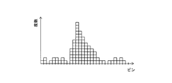
- the internal frequency is too low, in the histogram based on the time from the emission of light to the reception of reflected light, the distance measurement results are likely to be gathered in one bin, and the position estimation accuracy by fitting the probability density function will be reduced. There was a problem that it would end up.
- distance measuring device 1-1 Overall configuration of distance measuring device 1-2 Operation of distance measuring device 1-3 Modified example 2.
- FIG. 1 is a schematic configuration diagram showing an entire range finder according to a first embodiment of the present disclosure.
- the distance measuring device in FIG. 1 is a ToF distance measuring sensor.
- the distance measuring apparatus according to the first embodiment includes components such as a light projecting unit 1, a light receiving unit 2, a clock signal generating unit 3, a distance measuring processing unit 4, and a control unit 5. ing.
- these components may be integrally configured, for example, as a SoC (System on a chip) such as a CMOS (Complementary MOS) or an LSI (Large Scale Integration).
- the component may be configured as a separate LSI.
- the distance measuring device operates according to the clock signal output from the clock signal generation unit 3.
- the distance measuring device includes a communication IF unit 6 for outputting distance measurement data relating to the distance calculated by the distance measurement processing unit 4 to the outside.
- the distance measuring device is configured to be able to communicate with an external host IC via the communication IF unit 6.
- the light projecting unit 1 has a light source 8 that emits light 7 for ToF distance measurement.
- the light 7 for example, laser light can be used.
- the light source 8 may be, for example, an edge emitting semiconductor laser or a surface emitting semiconductor laser.
- the light source 8 is driven by the trigger pulse from the control unit 5.
- the trigger pulse is a pulsed signal having a predetermined frequency.
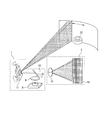
- the light projecting unit 1 also has a scanning mechanism for raster-scanning the light 7. In FIG. 2, as the scanning mechanism, a mirror scanning type scanning mechanism including an emitter lens 9, a light projecting mirror 10 and a micro mirror 11 is illustrated.
- the micro mirror 11 changes the direction of the reflecting surface according to the control signal from the control unit 5.
- the light 7 emitted from the light source 8 is emitted through the emitter lens 9, the light projecting mirror 10 and the micro mirror 11 in a direction corresponding to the direction of the reflecting surface of the micro mirror 11.
- the emitted light 7 is reflected by the object 12, and the reflected light 7 (hereinafter, also referred to as “reflected light 13”) is incident on the light receiving unit 2 via the micro mirror 11 and the light projecting mirror 10. ..
- the trigger pulse since the trigger pulse has a predetermined frequency and the light source 8 is configured to periodically emit light, the light 7 emitted from the light source 8 is applied to the same location of the object 12 multiple times, The reflected light 13 from the position irradiated with 7 is incident on the same portion (light receiving element 15) of the light receiving section 2 multiple times.
- the object 12 include a preceding vehicle of the own vehicle when the distance measuring device is mounted on the vehicle.
- the light receiving section 2 has a receiver lens 14 and a plurality of light receiving elements 15.
- the plurality of light receiving elements 15 are arranged in a two-dimensional array.
- a SPAD single photon avalanche diode
- the light receiving unit 2 collects the reflected light 13 incident through the micro mirror 11 and the light projecting mirror 10 by the receiver lens 14, and causes the light receiving element 15 according to the scanning direction of the light 7 to receive the light.
- the electric signal from the light receiving element 15 is output to the distance measurement processing unit 4.
- the clock signal generation unit 3 generates a clock signal (hereinafter, also referred to as “CLK signal”) according to the control signal from the control unit 5.
- CLK signal is output to the distance measurement processing unit 4.
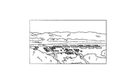
- the frequency of the CLK signal for example, when the range finder is mounted on the vehicle, if it is determined that there is no obstacle within a predetermined distance from the vehicle as shown in FIGS. 3A and 3B, the power consumption is reduced. So that it is set to a relatively low value.
- FIG. 3C when it is determined that an obstacle exists within a predetermined distance from the host vehicle, comparison is performed in order to investigate in detail the areas ⁇ , ⁇ , ⁇ where the obstacle exists on the road. Set to a very high value.
- the frequency of the CLK signal is reduced to perform the entire area search, and thereafter, only the areas ⁇ , ⁇ , and ⁇ determined to have an obstacle are investigated in detail by increasing the frequency of the CLK signal. Low power consumption may be achieved.
- the frequency of the CLK signal is, for example, when the range finder is mounted on the drone, as shown in FIGS. 4A and 4B, when it is determined that there is no obstacle within a predetermined distance from the drone, the power consumption is reduced. It is set to a relatively low value to reduce. On the other hand, when it is determined that the obstacle exists, a relatively high value is set in order to investigate the area where the obstacle exists in detail.
- the distance measurement processing unit 4 is a component that calculates the distance to the object 12 based on the timing when the light source 8 emits the light 7 and the timing when the light receiving unit 2 receives the reflected light 13.
- the distance measurement processing unit 4 is composed of, for example, a signal processor.
- the distance measurement processing unit 4 is configured to include a TDC (Time-to-Digital Converter) 16, a histogram creation unit 17, and a distance calculation unit 18. Based on the trigger pulse from the control unit 5 (trigger pulse for driving the light source 8) and the synchronization signal generated by the synchronization unit 20, the TDC 16 emits the light 7 from the light source 8 and then the reflected light 13 from the light receiving element 15.
- TDC Time-to-Digital Converter
- the TDC 16 constitutes a variation amplification section 19 and a synchronization section 20.
- the variation amplification unit 19 is a component that amplifies the variation in the temporal relative relationship between the electric signal output from the light receiving element 15 and the CLK signal output from the clock signal generation unit 3.
- the amplification amount of the variation is the bin width of the histograms shown in FIGS.
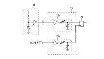
- the variation amplification unit 19 includes a first electric path 21, a plurality of first addition units 22 1 to 22 n (n is a natural number of 2 or more), and a first exclusive operation switch 23. Composed of.
- the second electric path 24, a plurality of second addition units 25 1 to 25 n, and a second exclusive operation switch 26 are also included.
- the first electric path 21 has one end connected to the input terminal 27 to which an electric signal is input from the light receiving element 15 and the other end connected to one end of the first switch 28 0 included in the first exclusive operation switch 23. It is a line. Then, the electric signal input from the light receiving element 15 is output to one end of the first switch 28 0 included in the first exclusive operation switch 23 via the first electric path 21.
- Each of the first addition portions 22 i (i is any of 1 to n) is arranged in parallel with the first electric path 21, and one end thereof is connected to the input terminal 27 to which an electric signal is input from the light receiving element 15.
- the other end is a signal path connected to one end of the first switch 28 i included in the first exclusive operation switch 23.
- the electric signal output from the light receiving element 15 is added to the jitter and output to one end of the first switch 28 i included in the first exclusive operation switch 23.
- Jitter is a fluctuation component that is generated in the time axis direction in a signal waveform and is very short in time.
- Each of the first adding units 22 1 to 22 n includes a NOT gate as shown in FIG. 8A, a NOR gate as shown in FIG. 8B, an AND gate as shown in FIG. 8C, and an XOR gate as shown in FIG. 8D. It may be configured by using one or more logic gates.
- the first adding units 22 1 to 22 n may be multistage delay circuits in which a large number of NOT gates are connected in series.
- the logic gate is composed of, for example, a plurality of transistors. Note that FIG. 9 exemplifies a configuration having only the first adding unit 22 1 as the first adding units 22 1 to 22 n .
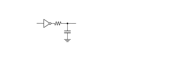
- each of the first adding units 22 1 to 22 n may be configured by using one or more RC circuits as shown in FIG. 10A.
- the signal edge can be made dull and the jitter can be further increased.
- the first adding units 22 1 to 22 n may be multi-stage circuits in which a large number of RC circuits are connected in series.
- the multistage circuit may be configured to include parallel paths and the like.
- the logic gate and the RC circuit may be combined and connected in series.
- a MOS ON resistance may be used as the resistor and a MOS parasitic capacitance may be used as the capacitor. As shown in FIGS.
- the resistance value of the resistor and the resistance value of the resistor may be used.
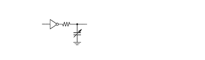
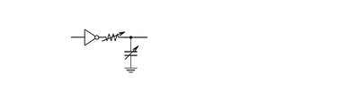
- One or both of the capacitance value of the capacitor may be changed. That is, the configuration may include one or both of the variable resistor and the variable capacitor.
- FIG. 11A illustrates a configuration in which only the capacitance value of the capacitor can be changed as the first adding units 22 1 to 22 n .
- FIG. 11A as the first adding units 22 1 to 22 n , only the first adding unit 22 1 is provided.
- FIG. 11B exemplifies a configuration in which both the resistance value of the resistor and the capacitance value of the capacitor can be changed as the first adding units 22 1 to 22 n .
- 0 “ ⁇ ” can be selected as the resistance value of the resistor and 0 “F” can be selected as the capacitance value of the capacitor
- the first exclusive operation switch 23 and the second exclusive operation switch 23 shown in FIG. 11A can be selected.
- the exclusive operation switch 26 is omitted. Note that, in FIG. 11B, as the first adding units 22 1 to 22 n , only the first adding unit 22 1 is provided.
- the first exclusive operation switch 23 when one first switch 28 j (j is any of 0 to n) is turned on, the remaining first switches 28 0 to 28 j-1 and 28 j+1 to 28. It is configured to include a plurality of first switches 28 0 to 28 n in which n is in the OFF state.
- the first switch 28 0 brings the other end of the first electric path 21 and the output terminal 29 connected to the synchronization unit 20 into a conductive state when the switch is in the ON state, and the first switch 28 0 when the switch is in the OFF state.
- the other end of 21 and the output terminal 29 connected to the synchronization unit 20 are cut off.
- the first switch 28 i When the first switch 28 i is in the ON state, it brings the other end of the first addition unit 22 i and the output terminal 29 connected to the synchronization unit 20 into a conductive state, and when in the OFF state, The other end of the 1 addition unit 22 i and the output terminal 29 connected to the synchronization unit 20 are cut off. Then, the first exclusive operation switch 23 turns on any one of the first switches 28 0 to 28 n in accordance with the path selection signal from the control unit 5, and sets the electric signal passing through the first electric path 21 to the first electric path 21. Any one of the electric signals to which the jitter is added, which is output from the adding units 22 1 to 22 n , is output to the synchronizing unit 20.
- the first exclusive operation switch 23 makes The switch 28 o is turned on, and the electric signal passing through the first electric path 21 is output to the synchronizing unit 20.
- the width of the bin is larger than the predetermined width, one of the first switches 28 1 to 28 n is turned on, and the electric signal added with the jitter output from the first adding unit 22 1 to 22 n Is output to the synchronization unit 20.
- Each of the first switches 28 0 , 28 1 to 28 n is realized by an analog method such as an NMOS switch shown in FIG. 12A, a PMOS switch shown in FIG. 12B, a CMOS switch shown in FIG. 12C, or the like. Good. When the analog method is used, the ON resistance of the MOS may increase the jitter of the electric signal passing through the first electric path 21. Further, each of the first switches 28 0 , 28 1 to 28 n may be realized by a logic method such as a NAND gate as shown in FIG. 13A and a NOR gate as shown in FIG. 13B.
- FIGS. 13A and 13B show a 2-input logic gate (NAND gate, NOR gate), a 3-input or higher logic gate may be used.
- the second electric path 24 has one end connected to the input terminal 30 to which the CLK signal output from the clock signal generation unit is input, and the other end connected to one end of the second switch 31 0 included in the second exclusive operation switch 26. It is a connected signal line. Then, the CLK signal is output to the one end of the second switch 31 0 included in the second exclusive operation switch 26 via the second electric path 24.
- Each of the second adding units 25 i is arranged in parallel with the second electric path 24, one end thereof is connected to the input terminal 30 to which the CLK signal is inputted from the clock signal generating unit 3, and the other end thereof is the second exclusive operation switch.
- 26 is a signal path connected to one end of the second switch 31 i included in 26. Then, the CLK signal is added with jitter (a short fluctuation component generated in the time axis direction) and output to one end of the second switch 31 i included in the second exclusive operation switch 26.
- jitter a short fluctuation component generated in the time axis direction
- Each of the second adding units 25 1 to 25 n is similar to the above-described first adding units 22 1 to 22 n in that the NOT gate shown in FIG. 8A, the NOR gate shown in FIG. 8B, and the FIG. 8C are shown.
- One or more logical gates such as an AND gate and an XOR gate as shown in FIG. 8D may be used.
- the second adding units 25 1 to 25 n may be multistage delay circuits in which a large number of NOT gates are connected in series. Note that FIG. 9 exemplifies a configuration having only the second adding unit 25 1 as the second adding units 25 1 to 25 n .
- each of the second adding units 25 1 to 25 n may be configured by using one or more RC circuits as shown in FIG. 10A.
- the second adding units 25 1 to 25 n may be multistage circuits in which a large number of RC circuits are connected in series.
- the multistage circuit may be configured to include parallel paths and the like.
- the logic gate and the RC circuit may be combined and connected in series.
- a MOS ON resistance may be used as the resistor and a MOS parasitic capacitance may be used as the capacitor. As shown in FIGS.
- FIG. 11A exemplifies a configuration in which only the capacitance value of the capacitor can be changed as the second adding units 25 1 to 25 n . Note that, in FIG. 11A, as the second adding units 25 1 to 25 n , only the second adding unit 25 1 is provided. Further, FIG. 11B exemplifies a configuration in which both the resistance value of the resistor and the capacitance value of the capacitor can be changed as the second adding units 25 1 to 25 n . In FIG.
- 0 “ ⁇ ” can be selected as the resistance value of the resistor and 0 “F” can be selected as the capacitance value of the capacitor, and the first exclusive operation switch 23 and the second exclusive operation switch 23 shown in FIG. 11A can be selected.
- the exclusive operation switch 26 is omitted. Note that, in FIG. 11B, as the second adding units 25 1 to 25 n , only the second adding unit 25 1 is provided.
- the configuration of the second adding units 25 1 to 25 n is preferably the same as the configuration of the first adding units 22 1 to 22 n , but it is not necessary to match them.
- the second exclusive operation switch 26 when one second switch 31 j is turned on, the remaining second switches 31 0 to 31 j-1 and 31 j+1 to 31 n are turned off. It is configured to include switches 31 0 to 31 n .
- the second switch 31 0 brings the other end of the second electric path 24 and the output terminal 32 connected to the synchronization unit 20 into conduction when it is in the ON state, and when it is in the OFF state, the second electric path The other end of 24 and the output terminal 32 connected to the synchronization unit 20 are cut off.
- the second switch 31 i brings the other end of the second addition section 25 i and the output terminal 32 connected to the synchronization section 20 into conduction when it is in the ON state, and when it is in the OFF state, The other end of the 2 addition unit 25 i and the output terminal 32 connected to the synchronization unit 20 are cut off. Then, the second exclusive operation switch 26 turns on any one of the second switches 31 0 to 31 n in accordance with the path selection signal from the control unit 5, sets the CLK signal passing through the second electric path 24, and Any of the jitter-added CLK signals output from the adding units 25 1 to 25 n is output to the synchronizing unit 20.
- the second exclusive operation switch 26 sets the second switch 31 o when the bin width of the histograms shown in FIGS. 5A, 5B, and 5C created by the histogram creation unit 17 is less than or equal to a predetermined width.
- the CLK signal passing through the second electric path 24 is output to the synchronizing unit 20.
- the width of the bin is larger than the predetermined width, one of the second switches 31 1 to 31 n is turned on, and the CLK signal added with the jitter output from the second adding units 25 1 to 25 n. Is output to the synchronization unit 20.
- the variation amplification unit 19 can add variation to one or both of the electrical signal output from the light receiving element 15 and the CLK signal output from the clock signal generation unit 3, and the variation between the electrical signal and the CLK signal can be provided. It is possible to amplify the variation in the temporal relative relationship.
- the synchronization unit 20 is a component that generates a synchronization signal that synchronizes the electrical signal after the variation is amplified with the CLK signal based on the electrical signal and the CLK signal after the variation is amplified by the variation amplification unit 19. More specifically, a synchronization signal that synchronizes the electric signal output from the first exclusive operation switch 23 with the CLK signal output from the second exclusive operation switch 26 is generated.
- the synchronization unit 20 is composed of, for example, a D flip-flop. With such a configuration, the TDC 16 receives the reflected light 13 by the light receiving element 15 after the light 7 is emitted from the light source 8 based on the trigger pulse from the control unit 5 and the synchronization signal generated by the synchronization unit 20.
- a method of measuring the arrival time for example, a method of measuring the time from the rise of the trigger pulse to the rise of the synchronization signal can be adopted.
- the histogram creating unit 17 is a component that creates a histogram as shown in FIGS. 5A, 5B, and 5C by accumulating each digital value (bin) converted by the TDC 16.
- the histogram of FIG. 5A is a histogram when the frequency of the CLK signal is relatively high.
- the histograms of FIGS. 5B and 5C are histograms when the frequency of the CLK signal is 1/10 of the frequency used to create the histogram of FIG. 5A.
- FIG. 5B is a histogram based on the electrical signal and the CLK signal that did not amplify the variation in the temporal relative relationship. Further, FIG.
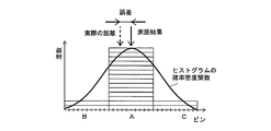
- 5C is a histogram based on the electrical signal and the CLK signal in which the variation in the temporal relative relationship is amplified. As shown in FIG. 5C, in the histogram based on the time from the emission of the light 7 to the reception of the reflected light 13 by increasing the variation in the temporal relative relationship between the electric signal from the light receiving element 15 and the CLK signal. It is possible to prevent the frequency of a certain section A from becoming significantly higher than the frequencies of the other sections B and C.
- the histogram is held as a kind of data structure or table on a memory (not shown), for example.
- the histogram is created for each light receiving element 15. That is, as many histograms as the number of the light receiving elements 15 are created.
- the distance calculation unit 18 refers to the histogram created by the histogram creation unit 17.
- the distance calculation unit 18 refers to each histogram created by the histogram creation unit 17 to detect a peak value (digital value) in the histogram, and from the arrival time corresponding to the detected peak value (digital value), It is a component that calculates the distance to the object 12.
- a histogram is fitted with a probability density function such as an ex-Gaussian distribution, and the peak value indicated by the probability density function obtained by the fitting can be adopted.
- the arrival time is the round-trip time to the object 12, and therefore the arrival time is c/2 (where c is The distance to the object 12 can be calculated for each light receiving element 15 by multiplying by the speed of light. Then, a distance image can be obtained from the distances calculated for each of the plurality of light receiving elements 15. Data (distance measurement data) related to the range image is output to the communication IF unit 6.
- the control unit 5 is a component that comprehensively controls the operation of the distance measuring device.
- the control unit 5 is composed of, for example, a microprocessor.
- the control unit 5 outputs a trigger pulse for emitting the light 7 to the light source 8 each time a predetermined light emission period elapses.
- the control unit 5 also outputs a control signal for setting the frequency of the CLK signal to the clock signal generation unit 3.
- the control signal is output each time the presence or absence of an obstacle around the vehicle, such as a vehicle equipped with the distance measuring device, changes.
- the control unit 5 also outputs a path selection signal to the first exclusive operation switch 23 and the second exclusive operation switch 26.
- the route selection signal is output, for example, when the frequency of the CLK signal is switched.
- the communication IF unit 6 is an interface circuit for outputting the distance measurement data calculated by the distance calculation unit 18 to an external host IC.
- the communication IF unit 6 may be, for example, an interface circuit compliant with MIPI (Mobile Industry Processor Interface), SPI (Serial Peripheral Interface) or I2C (Inter-Integrated Circuit), and these interfaces. It may be implemented with some of the circuits.
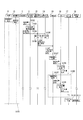
- FIG. 15 is a sequence diagram showing the operation of the distance measuring device according to the first embodiment.
- the light source 8 when executing the ToF distance measurement, the light source 8 is driven by the trigger pulse from the control unit 5, the light source 8 periodically emits the light 7, and the emitted light 7 is reflected from the object.
- the light 13 is received by the light receiving element 15, and electric signals are sequentially output (step S101).
- the control unit 5 since there is no obstacle around the vehicle or the like equipped with the distance measuring device, highly accurate distance measurement becomes unnecessary, and the control unit 5 lowers the frequency of the CLK signal as shown in FIG.
- the control signal having the value is output to the clock signal generation unit 3 (step S102). Then, the clock signal generation unit 3 switches the frequency of the CLK signal to a low value according to the control signal (step S103).
- the control unit 5 outputs the path selection signal to the first exclusive operation switch 23 and the second exclusive operation switch 26 (step S104). Then, the first exclusive operation switch 23 turns on any one of the first switch 28 1 to the first switch 28 n (for example, the first switch 28 1 ) according to the path selection signal (step S105).
- the jitter-added electric signal output from the first addition unit 22 1 (electric signal output from the light receiving element 15) is output to the synchronization unit 20.
- the second exclusive operation switch 26 turns on any one of the second switch 31 1 to the second switch 31 n (for example, the second switch 31 1 ) according to the path selection signal (step S106).
- the CLK signal (CLK signal generated by the clock signal generation unit 3) to which the jitter is added, which is output from the second addition unit 25 1 , is output to the synchronization unit 20. Therefore, the variation in the temporal relative relationship between the electric signal and the CLK signal is amplified.
- the synchronization unit 20 generates a synchronization signal by synchronizing the electric signal output from the first exclusive operation switch 23 with the CLK signal output from the second exclusive operation switch 26 (step S107). Then, the TDC 16 arrives from the time when the light 7 is emitted from the light source 8 to the time when the reflected light 13 is received by the light receiving element 15 based on the trigger pulse from the control unit 5 and the synchronization signal generated by the synchronization unit 20. The time is measured, and a digital value corresponding to the measured arrival time is generated (step S108). As a result, variations in digital value are amplified.
- the steps S107 to S108 are repeated to generate new synchronization signals one after another for each of the light 7 and the light receiving element 15 which are periodically emitted, and a digital signal corresponding to the arrival time is generated based on the generated synchronization signal. Values are generated one after another (step S109).
- the histogram creation unit 17 creates a histogram by accumulating each digital value (bin) converted by the TDC 16 (step S110). As a result, as shown in FIG. 5C, in the histogram, the frequency of the section A to which the true value of the distance belongs is reduced, and of the sections B and C adjacent to the section A, the frequency of the section B closer to the actual distance. Is increased more.
- the distance calculation unit 18 refers to each of the created histograms to detect a peak value (digital value) in the histogram, and from the arrival time corresponding to the detected peak value (digital value), the object 12 is detected.
- the distance to is calculated (step S111).
- the histogram is fitted with a probability density function such as an ex-Gaussian distribution, and the peak of the ex-Gaussian distribution indicated by the fitted function is used as the distance measurement result. It is possible to measure the distance to the object 12 with a resolution higher than the width. Then, by operating the scanning mechanism or the like, the distance image of the object 12 can be obtained by repeating the flow of steps S107 to S109 for all the light receiving elements 15.
- the distance measuring apparatus includes the variation amplification unit 19 that amplifies variation in the temporal relative relationship between the electrical signal output from the light receiving element 15 and the CLK signal. .. Then, first, in the synchronization unit 20, the synchronization signal is generated by synchronizing the electrical signal with the CLK signal based on the electrical signal and the CLK signal after the variation is amplified by the variation amplification unit 19. Then, the histogram creation unit 17 creates a histogram based on the time from the light source 8 emitting the light 7 to the reception of the reflected light 13 by the light receiving element 15 based on the synchronization signal generated by the synchronization unit 20. did.
- the distance calculation unit 18 calculates the distance to the object 12 based on the histogram created by the histogram creation unit 17. Therefore, in order to reduce power consumption, when the internal frequency is lowered, that is, when the frequency of the CLK signal is lowered, the variation in the temporal relative relationship between the electric signal from the light receiving element 15 and the CLK signal is reduced.
- the frequency of a certain section A becomes significantly larger than the frequencies of the other sections B and C. It can be prevented.
- the frequency of the section B closer to the actual distance can be further increased.
- the width is higher than the width of the section A.
- the distance to the object 12 can be measured. Therefore, it is possible to provide a distance measuring device that can improve measurement accuracy while reducing power consumption.
- the variation amplification unit 19 adds jitter to at least one of the electrical signal and the CLK signal output from the light receiving element 15. Therefore, it is possible to easily amplify the variation in the temporal relative relationship between the electric signal and the CLK signal.
- the electrical signal is input, the first adding units 22 1 to 22 n that add and output the jitter to the electrical signal, and the CLK signal are input, and the jitter is added to the CLK signal.
- the CLK signal after the jitter is added has time according to the probability density function of the variation due to the added jitter. It will start to vary in the axial direction.
- each of the first adding units 22 1 to 22 n and the second adding units 25 1 to 25 n includes at least one of a logic gate and an RC circuit. did. Therefore, the first adding units 22 1 to 22 n and the second adding units 25 1 to 25 n can be easily configured.
- the logic gates are connected in series to form a multi-stage delay circuit. Therefore, the jitter can be increased.
- the resistor of the RC circuit is a variable resistor. Therefore, it is not necessary to prepare a plurality of first adding units 22 1 to 22 n and second adding units 25 1 to 25 n .
- the capacitor of the RC circuit is a variable capacitor. Therefore, it is not necessary to prepare a plurality of first adding units 22 1 to 22 n and second adding units 25 1 to 25 n .
- the first electric path 21 that is arranged in parallel with the first adding units 22 1 to 22 n and that allows the electric signal output from the light receiving element 15 to pass therethrough is provided.
- a first exclusive operation switch 23 that outputs to the synchronization unit 20 either the electric signal to which the jitter is added output from the first addition units 22 1 to 22 n or the electric signal that passes through the first electric path 21. I was prepared.
- the second electrical path 24, which is arranged in parallel with the second adding units 25 1 to 25 n passes the CLK signal, and the jitter added CLK output from the second adding units 25 1 to 25 n.
- the second exclusive operation switch 26 that outputs either the signal or the CLK signal that passes through the second electric path 24 to the synchronization unit 20 is provided. Then, the synchronization unit 20 generates a synchronization signal by synchronizing the electric signal output from the first exclusive operation switch 23 with the CLK signal output from the second exclusive operation switch 26. Therefore, it is possible to easily generate various synchronization signals such as a synchronization signal in which jitter is added only to an electric signal, a synchronization signal in which jitter is added only to a CLK signal, and a synchronization signal in which jitter is added to both of them. it can.
- the electric signal passing through the first electric path 21 is transmitted.
- the output is made to the synchronization unit 20.
- the second exclusive operation switch 26 when the bin width of the histogram is equal to or smaller than the predetermined width, the electric signal passing through the second electric path 24 is output to the synchronizing unit 20. Therefore, when the bin width of the histogram is narrow and the measurement accuracy is high, it is not necessary to amplify the variation, and it is possible to prevent the measurement accuracy from decreasing.
- each of the first exclusive operation switch 23 and the second exclusive operation switch 26 includes any one of an NMOS switch, a PMOS switch, a CMOS switch, a NAND gate and a NOR gate. I chose Therefore, the first exclusive operation switch 23 and the second exclusive operation switch 26 can be easily configured.
- the variation amplification unit 19 sets the variation amplification amount to 1/3 or more and 1/2 or less of the bin width of the histogram. Therefore, it is possible to reduce the frequency of a certain section A of the histogram and increase the frequency of the adjacent sections B and C.
- the first addition units 22 1 to 22 n are used as the variation amplification unit 19 in order to add jitter to the electric signal output from the light receiving element 15.
- the variation amplification unit 19 as shown in FIG. 16, a voltage control unit 33 that controls the voltage between the anode and the cathode of the SPAD that is the light receiving element 15 is used so that jitter is added to the electric signal. Good.
- the smaller the inclination angle b the more time it takes to generate avalanche and the increase in jitter.
- a wavelength control unit 34 that controls the wavelength of the light 7 emitted from the light source 8 may be used so that jitter is added to the electric signal.
- a temperature control unit 35 that controls the temperature of the light receiving element 15 so that jitter is added to the electric signal may be used.
- the technology according to the present disclosure can be applied to various products.
- the technology according to the present disclosure is applicable to any type of movement such as an automobile, an electric vehicle, a hybrid electric vehicle, a motorcycle, a bicycle, a personal mobility, an airplane, a drone, a ship, a robot, a construction machine, and an agricultural machine (tractor). It may be realized as a device mounted on the body.
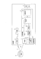
- FIG. 20 is a block diagram showing a schematic configuration example of a vehicle control system 7000 that is an example of a mobile body control system to which the technology according to the present disclosure can be applied.
- the vehicle control system 7000 includes a plurality of electronic control units connected via a communication network 7010.
- the vehicle control system 7000 includes a drive system control unit 7100, a body system control unit 7200, a battery control unit 7300, a vehicle exterior information detection unit 7400, a vehicle interior information detection unit 7500, and an integrated control unit 7600. ..
- the communication network 7010 connecting these plural control units complies with any standard such as CAN (Controller Area Network), LIN (Local Interconnect Network), LAN (Local Area Network), or FlexRay (registered trademark). It may be an in-vehicle communication network.
- CAN Controller Area Network
- LIN Local Interconnect Network
- LAN Local Area Network
- FlexRay registered trademark
- Each control unit includes a microcomputer that performs arithmetic processing according to various programs, a storage unit that stores a program executed by the microcomputer or parameters used for various arithmetic operations, and a drive circuit that drives various controlled devices. Equipped with.
- Each control unit is equipped with a network I/F for communicating with other control units via the communication network 7010, and also by wire communication or wireless communication with devices or sensors inside or outside the vehicle. A communication I/F for performing communication is provided. In FIG.
- a microcomputer 7610 As the functional configuration of the integrated control unit 7600, a microcomputer 7610, a general-purpose communication I/F 7620, a dedicated communication I/F 7630, a positioning unit 7640, a beacon receiving unit 7650, an in-vehicle device I/F 7660, a voice image output unit 7670, An in-vehicle network I/F 7680 and a storage unit 7690 are illustrated.
- the other control units also include a microcomputer, a communication I/F, a storage unit, and the like.
- the drive system control unit 7100 controls the operation of devices related to the drive system of the vehicle according to various programs.
- the drive system control unit 7100 includes a drive force generation device for generating a drive force of a vehicle such as an internal combustion engine or a drive motor, a drive force transmission mechanism for transmitting the drive force to wheels, and a steering angle of the vehicle. It functions as a steering mechanism for adjusting and a control device such as a braking device for generating a braking force of the vehicle.
- the drive system control unit 7100 may have a function as a control device such as ABS (Antilock Brake System) or ESC (Electronic Stability Control).
- a vehicle state detection unit 7110 is connected to the drive system control unit 7100.
- the vehicle state detection unit 7110 includes, for example, a gyro sensor that detects the angular velocity of the axial rotation motion of the vehicle body, an acceleration sensor that detects the acceleration of the vehicle, or an accelerator pedal operation amount, a brake pedal operation amount, or a steering wheel steering operation. At least one of sensors for detecting an angle, an engine speed, a wheel rotation speed, and the like is included.
- the drive system control unit 7100 performs arithmetic processing using a signal input from the vehicle state detection unit 7110 to control the internal combustion engine, drive motor, electric power steering device, brake device, or the like.
- the body system control unit 7200 controls the operation of various devices mounted on the vehicle body according to various programs.
- the body system control unit 7200 functions as a keyless entry system, a smart key system, a power window device, or a control device for various lamps such as a head lamp, a back lamp, a brake lamp, a winker, or a fog lamp.
- the body system control unit 7200 may receive radio waves or signals of various switches transmitted from a portable device that substitutes for a key.
- the body system control unit 7200 receives the input of these radio waves or signals and controls the vehicle door lock device, the power window device, the lamp, and the like.
- the battery control unit 7300 controls the secondary battery 7310 that is the power supply source of the drive motor according to various programs. For example, the battery control unit 7300 receives information such as the battery temperature, the battery output voltage, and the remaining capacity of the battery from the battery device including the secondary battery 7310. The battery control unit 7300 performs arithmetic processing using these signals to perform temperature control control of the secondary battery 7310 or control of a cooling device or the like included in the battery device.
- the exterior information detection unit 7400 detects information outside the vehicle equipped with the vehicle control system 7000.
- the image pickup unit 7410 and the vehicle exterior information detection unit 7420 is connected to the vehicle exterior information detection unit 7400.
- the imaging unit 7410 includes at least one of a ToF (Time Of Flight) camera, a stereo camera, a monocular camera, an infrared camera, and other cameras.
- the outside-vehicle information detection unit 7420 detects, for example, an environment sensor for detecting the current weather or weather, or another vehicle around the vehicle equipped with the vehicle control system 7000, an obstacle, a pedestrian, or the like. At least one of the ambient information detection sensors of.
- the environment sensor may be, for example, at least one of a raindrop sensor that detects rainy weather, a fog sensor that detects fog, a sunshine sensor that detects the degree of sunshine, and a snow sensor that detects snowfall.
- the ambient information detection sensor may be at least one of an ultrasonic sensor, a radar device, and a LIDAR (Light Detection and Ranging, Laser Imaging Detection and Ranging) device.
- the image pickup unit 7410 and the vehicle exterior information detection unit 7420 may be provided as independent sensors or devices, or may be provided as a device in which a plurality of sensors or devices are integrated.
- FIG. 21 shows an example of installation positions of the image pickup unit 7410 and the vehicle exterior information detection unit 7420.
- the imaging units 7910, 7912, 7914, 7916, 7918 are provided at at least one of the front nose of the vehicle 7900, the side mirrors, the rear bumper, the back door, and the upper part of the windshield in the vehicle interior.
- An image capturing unit 7910 provided on the front nose and an image capturing unit 7918 provided on the upper part of the windshield in the vehicle interior mainly acquire an image in front of the vehicle 7900.
- the imaging units 7912 and 7914 included in the side mirrors mainly acquire images of the side of the vehicle 7900.
- the imaging unit 7916 provided in the rear bumper or the back door mainly acquires an image of the rear of the vehicle 7900.
- the imaging unit 7918 provided on the upper part of the windshield in the vehicle interior is mainly used for detecting a preceding vehicle, a pedestrian, an obstacle, a traffic signal, a traffic sign, a lane, or the like.
- FIG. 21 shows an example of the shooting ranges of the respective image pickup units 7910, 7912, 7914, 7916.
- the imaging range a indicates the imaging range of the imaging unit 7910 provided on the front nose
- the imaging ranges b and c indicate the imaging ranges of the imaging units 7912 and 7914 provided on the side mirrors
- the imaging range d is The imaging range of the imaging part 7916 provided in the rear bumper or the back door is shown. For example, by overlaying the image data captured by the image capturing units 7910, 7912, 7914, and 7916, a bird's-eye view image of the vehicle 7900 viewed from above can be obtained.
- the vehicle exterior information detection units 7920, 7922, 7924, 7926, 7928, 7930 provided on the front, rear, sides, corners of the vehicle 7900 and on the windshield in the vehicle interior may be ultrasonic sensors or radar devices, for example.
- the vehicle exterior information detection units 7920, 7926, 7930 provided on the front nose, rear bumper, back door, and upper windshield of the vehicle 7900 may be, for example, LIDAR devices.
- These vehicle exterior information detection units 7920 to 7930 are mainly used to detect a preceding vehicle, a pedestrian, an obstacle, or the like.
- the vehicle exterior information detection unit 7400 causes the image capturing unit 7410 to capture an image of the vehicle exterior and receives the captured image data. Further, the vehicle exterior information detection unit 7400 receives the detection information from the vehicle exterior information detection unit 7420 connected thereto.
- the vehicle exterior information detection unit 7420 is an ultrasonic sensor, a radar device, or a LIDAR device
- the vehicle exterior information detection unit 7400 transmits ultrasonic waves, electromagnetic waves, or the like, and receives information on the received reflected waves.
- the vehicle exterior information detection unit 7400 may perform object detection processing or distance detection processing such as people, vehicles, obstacles, signs, or characters on the road surface based on the received information.
- the vehicle exterior information detection unit 7400 may perform environment recognition processing for recognizing rainfall, fog, road surface conditions, or the like based on the received information.
- the vehicle exterior information detection unit 7400 may calculate the distance to an object outside the vehicle based on the received information.
- the vehicle exterior information detection unit 7400 may also perform image recognition processing or distance detection processing for recognizing a person, a car, an obstacle, a sign, characters on the road surface, or the like based on the received image data.
- the vehicle exterior information detection unit 7400 performs processing such as distortion correction or position adjustment on the received image data, combines the image data captured by different image capturing units 7410, and generates an overhead image or a panoramic image. Good.
- the vehicle exterior information detection unit 7400 may perform viewpoint conversion processing using image data captured by different image capturing units 7410.
- the in-vehicle information detection unit 7500 detects in-vehicle information.
- a driver state detection unit 7510 that detects the state of the driver is connected.
- the driver state detection unit 7510 may include a camera that captures an image of the driver, a biometric sensor that detects biometric information of the driver, a microphone that collects voice in the vehicle, and the like.
- the biometric sensor is provided on, for example, a seat surface or a steering wheel, and detects biometric information of an occupant sitting on a seat or a driver who holds the steering wheel.
- the in-vehicle information detection unit 7500 may calculate the degree of fatigue or concentration of the driver based on the detection information input from the driver state detection unit 7510, or determine whether the driver is asleep. You may.
- the in-vehicle information detection unit 7500 may perform processing such as noise canceling processing on the collected audio signal.
- the integrated control unit 7600 controls overall operations in the vehicle control system 7000 according to various programs.
- An input unit 7800 is connected to the integrated control unit 7600.
- the input unit 7800 is realized by a device that can be input and operated by a passenger, such as a touch panel, a button, a microphone, a switch or a lever. Data obtained by voice recognition of voice input by a microphone may be input to the integrated control unit 7600.
- the input unit 7800 may be, for example, a remote control device that uses infrared rays or other radio waves, or may be an external connection device such as a mobile phone or a PDA (Personal Digital Assistant) that supports the operation of the vehicle control system 7000. May be.
- the input unit 7800 may be, for example, a camera, in which case the passenger can input information by gesture. Alternatively, data obtained by detecting the movement of the wearable device worn by the passenger may be input. Further, the input unit 7800 may include, for example, an input control circuit that generates an input signal based on information input by a passenger or the like using the input unit 7800 and outputs the input signal to the integrated control unit 7600. A passenger or the like operates the input unit 7800 to input various data to the vehicle control system 7000 and instruct a processing operation.
- the storage unit 7690 may include a ROM (Read Only Memory) that stores various programs executed by the microcomputer, and a RAM (Random Access Memory) that stores various parameters, calculation results, sensor values, and the like.
- the storage unit 7690 may be realized by a magnetic storage device such as an HDD (Hard Disc Drive), a semiconductor storage device, an optical storage device, a magneto-optical storage device, or the like.
- the general-purpose communication I/F 7620 is a general-purpose communication I/F that mediates communication with various devices existing in the external environment 7750.
- the general-purpose communication I/F 7620 is a cellular communication protocol such as GSM (registered trademark) (Global System of Mobile communications), WiMAX (registered trademark), LTE (registered trademark) (Long Term Evolution), or LTE-A (LTE-Advanced).
- GSM Global System of Mobile communications
- WiMAX registered trademark
- LTE registered trademark
- LTE-A Long Term Evolution
- LTE-A Long Term Evolution-Advanced
- a wireless LAN also referred to as Wi-Fi (registered trademark)
- Bluetooth registered trademark
- the general-purpose communication I/F 7620 is connected to a device (for example, an application server or a control server) existing on an external network (for example, the Internet, a cloud network, or a network unique to a business operator) via a base station or an access point, for example. You may.
- the general-purpose communication I/F 7620 uses, for example, the P2P (Peer To Peer) technology, and is a terminal existing in the vicinity of the vehicle (for example, a driver, a pedestrian or a shop terminal, or an MTC (Machine Type Communication) terminal). You may connect with.
- P2P Peer To Peer
- MTC Machine Type Communication
- the dedicated communication I/F 7630 is a communication I/F that supports a communication protocol formulated for use in a vehicle.
- the dedicated communication I/F 7630 uses a standard protocol such as WAVE (Wireless Access in Vehicle Environment), DSRC (Dedicated Short Range Communications), or a cellular communication protocol, which is a combination of a lower layer IEEE 802.11p and an upper layer IEEE 1609, for example. May be implemented.
- the dedicated communication I/F 7630 is typically a vehicle-to-vehicle communication, a vehicle-to-infrastructure communication, a vehicle-to-home communication, and a pedestrian-to-pedestrian communication (Vehicle to Pedestrian). ) Perform V2X communications, a concept that includes one or more of the communications.
- the positioning unit 7640 receives, for example, a GNSS signal from a GNSS (Global Navigation Satellite System) satellite (for example, a GPS signal from a GPS (Global Positioning System) satellite) to perform positioning, and the latitude, longitude, and altitude of the vehicle.
- the position information including is generated.
- the positioning unit 7640 may specify the current position by exchanging signals with the wireless access point, or may acquire position information from a terminal having a positioning function, such as a mobile phone, PHS, or smartphone.
- the beacon receiving unit 7650 receives, for example, a radio wave or an electromagnetic wave transmitted from a wireless station or the like installed on the road, and acquires information such as the current position, traffic jam, traffic closure, or required time.
- the function of beacon receiving unit 7650 may be included in dedicated communication I/F 7630 described above.
- the in-vehicle device I/F 7660 is a communication interface that mediates a connection between the microcomputer 7610 and various in-vehicle devices 7760 existing in the vehicle.
- the in-vehicle device I/F 7660 may establish a wireless connection using a wireless communication protocol such as a wireless LAN, Bluetooth (registered trademark), NFC (Near Field Communication) or WUSB (Wireless USB). Further, the in-vehicle device I/F 7660 is connected to a USB (Universal Serial Bus), HDMI (registered trademark) (High-Definition Multimedia Interface), or MHL (Mobile) via a connection terminal (and a cable if necessary) not shown. Wired connection such as High-definition Link) may be established.
- the in-vehicle device 7760 may include, for example, at least one of a mobile device or a wearable device that an occupant has, or an information device that is carried in or attached to a vehicle.
- the in-vehicle device 7760 may include a navigation device that searches for a route to an arbitrary destination.
- the in-vehicle device I/F 7660 exchanges control signals or data signals with these in-vehicle devices 7760.
- the in-vehicle network I/F 7680 is an interface that mediates communication between the microcomputer 7610 and the communication network 7010.
- the vehicle-mounted network I/F 7680 transmits and receives signals and the like according to a predetermined protocol supported by the communication network 7010.
- the microcomputer 7610 of the integrated control unit 7600 passes through at least one of a general-purpose communication I/F 7620, a dedicated communication I/F 7630, a positioning unit 7640, a beacon receiving unit 7650, an in-vehicle device I/F 7660, and an in-vehicle network I/F 7680.
- the vehicle control system 7000 is controlled according to various programs based on the information acquired by the above. For example, the microcomputer 7610 calculates a control target value of the driving force generation device, the steering mechanism or the braking device based on the acquired information on the inside and outside of the vehicle, and outputs a control command to the drive system control unit 7100. Good.
- the microcomputer 7610 realizes the functions of ADAS (Advanced Driver Assistance System) including avoidance or impact mitigation of a vehicle, follow-up traveling based on an inter-vehicle distance, vehicle speed maintenance traveling, vehicle collision warning, vehicle lane departure warning, etc. You may perform the coordinated control aiming at.
- the microcomputer 7610 controls the driving force generation device, the steering mechanism, the braking device, and the like based on the acquired information about the surroundings of the vehicle, so that the microcomputer 7610 automatically travels independently of the driver's operation. You may perform the cooperative control aiming at driving etc.
- ADAS Advanced Driver Assistance System
- a general-purpose communication I/F 7620 a dedicated communication I/F 7630, a positioning unit 7640, a beacon receiving unit 7650, an in-vehicle device I/F 7660, and an in-vehicle network I/F 7680.
- the microcomputer 7610 may generate a warning signal by predicting a danger such as a vehicle collision, a pedestrian or the like approaching or entering a closed road, based on the acquired information.
- the warning signal may be, for example, a signal for generating a warning sound or turning on a warning lamp.
- the voice image output unit 7670 transmits an output signal of at least one of a voice and an image to an output device capable of visually or audibly notifying information to a passenger of the vehicle or the outside of the vehicle.
- an audio speaker 7710, a display unit 7720, and an instrument panel 7730 are illustrated as output devices.
- the display unit 7720 may include at least one of an onboard display and a head-up display, for example.
- the display unit 7720 may have an AR (Augmented Reality) display function.
- the output device may be a device other than these devices, such as headphones, a wearable device such as a glasses-type display worn by a passenger, a projector, or a lamp.
- the output device When the output device is a display device, the display device displays results obtained by various processes performed by the microcomputer 7610 or information received from another control unit in various formats such as text, images, tables, and graphs. Display it visually.
- the output device is a voice output device, the voice output device converts an audio signal composed of reproduced voice data, acoustic data, or the like into an analog signal and outputs it audibly.
- At least two control units connected via the communication network 7010 may be integrated as one control unit.
- each control unit may be composed of a plurality of control units.
- the vehicle control system 7000 may include another control unit not shown.
- some or all of the functions of one of the control units may be given to another control unit. That is, if the information is transmitted and received via the communication network 7010, the predetermined arithmetic processing may be performed by any one of the control units.
- a sensor or device connected to one of the control units may be connected to another control unit, and a plurality of control units may send and receive detection information to and from each other via the communication network 7010. .
- the distance measuring device can be applied to the vehicle exterior information detection unit 7420 of the application example shown in FIG.
- the distance measuring device can calculate the distance to an obstacle in front of the vehicle 7900.
- the present technology may have the following configurations.
- a light source that emits light
- a light-receiving element that receives reflected light from an object that has reflected the light
- a variation amplifier for amplifying variation in the temporal relative relationship between the electric signal and the clock signal output from the light receiving element
- a synchronization unit that generates a synchronization signal by synchronizing the electrical signal with the clock signal based on the electrical signal and the clock signal after the variation is amplified by the variation amplification unit
- a histogram creation unit that creates a histogram based on the time from when the light source emits light to when the reflected light is received by the light receiving element
- a distance calculation unit that calculates a distance to the object based on the histogram created by the histogram creation unit.
- a first electric path that is arranged in parallel with the first adding unit and that passes the electric signal output from the light receiving element;
- a first exclusive operation switch that outputs to the synchronization unit any one of the electric signal to which the jitter is added, which is output from the first addition unit, and the electric signal that passes through the first electric path;
- a second electrical path that is arranged in parallel with the second adding section and that passes the clock signal;
- a second exclusive operation switch for outputting to the synchronization unit any one of the clock signal added with the jitter output from the second addition unit and the clock signal passing through the second electric path.
- the synchronization unit generates a synchronization signal by synchronizing the electric signal output from the first exclusive operation switch with the clock signal output from the second exclusive operation switch. (3) to (7) The distance measuring device according to any one of 1. (9)
- the first exclusive operation switch outputs the electric signal passing through the first electric path to the synchronization unit when the width of the bin of the histogram is equal to or less than a predetermined width.
- the second exclusive operation switch outputs the electric signal passing through the second electric path to the synchronization unit when the width of the bin of the histogram is less than or equal to a predetermined width, The described distance measuring device.
- Each of the first exclusive operation switch and the second exclusive operation switch includes any one of an NMOS switch, a PMOS switch, a CMOS switch, a NAND gate and a NOR gate.
- Distance device. (11)
- the variation amplification unit is the distance measuring apparatus according to any one of (1) to (10), wherein the variation amplification amount is 1/3 or more and 1/2 or less of a bin width of the histogram.
- the light receiving element is a SPAD, The range finder according to (1), wherein the variation amplifier controls the anode-cathode voltage of the SPAD so that jitter is added to the electric signal.
- the variation amplification unit controls the temperature of the light receiving element so that jitter is added to the electric signal.
- the light source periodically emits light, the reflected light from the object that reflects the emitted light is received by the light receiving element, and electrical signals are output one after another, and the output electrical signal and the clock signal are temporally changed.
- a synchronization signal is generated one after another by synchronizing the electrical signal with the clock signal based on the electrical signal and the clock signal after the variation of the relative relationship is amplified, and the generated synchronization signal is generated.
- a histogram based on the time from the light source emitting light to the time when the light receiving element receives the reflected light is created, and the distance to the object is calculated based on the created histogram.
- SYMBOLS 1 Distance measuring device, 2... Light emitting part, 3... Light receiving part, 4... Distance measuring processing part, 5... Control part, 6... Communication IF part, 7... Light, 8... Light source, 9... Emitter lens, 10... Projection mirror, 11... Micro mirror, 12... Object, 13... Reflected light, 14... Receiver lens, 16... TDC, 15... Light receiving element, 17... Histogram creating section, 18... Distance calculating section, 19... Variation amplification section , 20... Synchronizing unit, 21... First electric path, 22 1 to 22 n ... First adding unit, 23... First exclusive operation switch, 24... Second electric path, 25 1 to 25 n ... Second adding unit, 26... Second exclusive operation switch, 27...
Landscapes
- Engineering & Computer Science (AREA)
- Physics & Mathematics (AREA)
- Computer Networks & Wireless Communication (AREA)
- General Physics & Mathematics (AREA)
- Radar, Positioning & Navigation (AREA)
- Remote Sensing (AREA)
- Electromagnetism (AREA)
- Optical Radar Systems And Details Thereof (AREA)
Abstract
消費電力を低減しつつ、測定精度を向上できる測距装置を提供する。ばらつき増幅部で、受光素子から出力される電気信号と、クロック生成部で生成されるクロック信号との時間的な相対関係のばらつきを増幅させる。続いて、同期部で、ばらつき増幅部でばらつきが増幅された後の電気信号及びクロック信号に基づき、その電気信号をそのクロック信号に同期させることで同期信号を生成する。続いて、ヒストグラム作成部で、同期部で生成した同期信号に基づき、光源が光を発してから受光素子で反射光を受光するまでの時間に基づくヒストグラムを作成する。続いて、距離算出部で、ヒストグラム作成部で作成したヒストグラムに基づき、対象物までの距離を算出する。
Description
本技術は、測距装置及び測距方法に関する。
近年、対象物までの距離を直接ToF(Time of Flight)を用いて計測する測距装置が提案されている(例えば、特許文献1参照。)。特許文献1に記載の測距装置では、光源が光を発してから受光素子で反射光を受光するまでの時間を多数回測定し、測定した多数回の時間に基づくヒストグラムを用いて、測距精度を向上するようになっている。
しかし、このような測距装置では、低消費電力化と測距精度向上とが求められている。
本開示は、消費電力を低減しつつ、測定精度を向上できる測距装置及び測距方法を提供することを目的とする。
本開示は、消費電力を低減しつつ、測定精度を向上できる測距装置及び測距方法を提供することを目的とする。
本開示の測距装置は、(a)光を発する光源と、(b)光を反射した対象物からの反射光を受光する受光素子と、(c)受光素子から出力される電気信号とクロック信号との時間的な相対関係のばらつきを増幅させるばらつき増幅部と、(d)ばらつき増幅部でばらつきが増幅された電気信号を当該ばらつきが増幅されたクロック信号に同期させることで同期信号を生成する同期部と、(e)同期部で生成した同期信号に基づき、光源が光を発してから受光素子で反射光を受光するまでの時間に基づくヒストグラムを作成するヒストグラム作成部と、(f)ヒストグラム作成部で作成したヒストグラムに基づき、対象物までの距離を算出する距離算出部と、を備える。
本開示の測距方法は、(a)光源からの光を反射した対象物からの反射光を受光素子で受光して電気信号を出力し、(b)出力された電気信号とクロック信号との時間的な相対関係のばらつきを増幅させ、(c)ばらつきが増幅された後の電気信号及びクロック信号に基づき、電気信号をクロック信号に同期させることで同期信号を生成し、(d)生成した同期信号に基づき、光源が光を発してから受光素子で反射光を受光するまでの時間に基づくヒストグラムを作成し、(e)作成したヒストグラムに基づき、対象物までの距離を算出する。
本発明者らは、測距装置において、精度の高い測距が必要な場合に、内部周波数を高くし、精度の高い測距が不要な場合に内部周波数を低くすることを考えた。しかし、内部周波数が低すぎると、光を発してから反射光を受光するまでの時間に基づくヒストグラムにおいて、一つのbinに測距結果が集まりやすく、確率密度関数のフィッティングによる位置推定精度が低下してしまうという問題があった。
以下に、本開示の実施形態に係る測距装置及び測距方法の一例を、図1~図21を参照しながら説明する。本開示の実施形態は、以下の順序で説明する。なお、本開示は、以下の例に限定されるものではない。また、本明細書に記載された効果はあくまで例示であって限定されるものでは無く、また他の効果があってもよい。
1.第1の実施形態:測距装置
1-1 測距装置の全体構成
1-2 測距装置の動作
1-3 変形例
2.応用例:移動体制御システム
1-1 測距装置の全体構成
1-2 測距装置の動作
1-3 変形例
2.応用例:移動体制御システム
〈1.第1の実施形態〉
[1-1 測距装置の全体構成]
図1は、本開示の第1の実施形態に係る測距装置の全体を示す概略構成図である。図1の測距装置は、ToF測距センサである。図1に示すように、第1の実施形態の測距装置は、投光部1と、受光部2と、クロック信号生成部3と、測距処理部4と、制御部5といったコンポーネントを備えている。これらのコンポーネントは、例えば、CMOS(Complementary MOS)、LSI(Large Scale Integration)のようなSoC(System on a chip)として一体的に構成してもよく、投光部1や受光部2といった幾つかのコンポーネントを別体のLSIとして構成してもよい。測距装置は、クロック信号生成部3から出力されるクロック信号に従って動作する。測距装置は、測距処理部4で算出された距離に係る測距データを外部に出力するための通信IF部6を含んでいる。図示されていないが、測距装置は、通信IF部6を介して、外部のホストICと通信可能に構成されている。
[1-1 測距装置の全体構成]
図1は、本開示の第1の実施形態に係る測距装置の全体を示す概略構成図である。図1の測距装置は、ToF測距センサである。図1に示すように、第1の実施形態の測距装置は、投光部1と、受光部2と、クロック信号生成部3と、測距処理部4と、制御部5といったコンポーネントを備えている。これらのコンポーネントは、例えば、CMOS(Complementary MOS)、LSI(Large Scale Integration)のようなSoC(System on a chip)として一体的に構成してもよく、投光部1や受光部2といった幾つかのコンポーネントを別体のLSIとして構成してもよい。測距装置は、クロック信号生成部3から出力されるクロック信号に従って動作する。測距装置は、測距処理部4で算出された距離に係る測距データを外部に出力するための通信IF部6を含んでいる。図示されていないが、測距装置は、通信IF部6を介して、外部のホストICと通信可能に構成されている。
投光部1は、図2に示すように、ToF測距のための光7を発する光源8を有している。光7としては、例えば、レーザ光を用いることができる。光源8としては、例えば、端面発光型半導体レーザであってもよく、面発光型半導体レーザであってもよい。光源8は、制御部5からのトリガパルスによって駆動される。トリガパルスは、所定の周波数を有するパルス状の信号である。また、投光部1は、光7をラスタスキャンするためのスキャン機構を有している。図2では、スキャン機構として、エミッタレンズ9、投光ミラー10、及びマイクロミラー11を含むミラースキャン型のスキャン機構を例示している。
マイクロミラー11は、制御部5からの制御信号に従って、反射面の向きを変更する。そして、光源8が発した光7を、エミッタレンズ9、投光ミラー10及びマイクロミラー11を介してマイクロミラー11の反射面の向きに応じた方向に出射する。出射された光7は、対象物12で反射して、反射した光7(以下、「反射光13」とも呼ぶ)がマイクロミラー11及び投光ミラー10を介して、受光部2に入射される。その際、トリガパルスが所定の周波数を有し、光源8が周期的に発光するようになっているため、光源8から発せられた光7は対象物12の同じ箇所に複数回照射され、光7が照射された位置からの反射光13は受光部2の同じ箇所(受光素子15)に複数回入射される。対象物12としては、例えば、測距装置が車両に搭載されている場合自車両の先行車両等が挙げられる。
マイクロミラー11は、制御部5からの制御信号に従って、反射面の向きを変更する。そして、光源8が発した光7を、エミッタレンズ9、投光ミラー10及びマイクロミラー11を介してマイクロミラー11の反射面の向きに応じた方向に出射する。出射された光7は、対象物12で反射して、反射した光7(以下、「反射光13」とも呼ぶ)がマイクロミラー11及び投光ミラー10を介して、受光部2に入射される。その際、トリガパルスが所定の周波数を有し、光源8が周期的に発光するようになっているため、光源8から発せられた光7は対象物12の同じ箇所に複数回照射され、光7が照射された位置からの反射光13は受光部2の同じ箇所(受光素子15)に複数回入射される。対象物12としては、例えば、測距装置が車両に搭載されている場合自車両の先行車両等が挙げられる。
受光部2は、レシーバレンズ14と、複数の受光素子15とを有している。複数の受光素子15は、二次元のアレイ状に配置される。受光素子15としては、例えば、受光した光に反応して電気信号を出力するSPAD(single photon avalanche diode)を用いることができる。そして、受光部2は、マイクロミラー11及び投光ミラー10を介して入射された反射光13を、レシーバレンズ14で集光して、光7のスキャン方向に応じた受光素子15に受光させる。受光素子15からの電気信号は、測距処理部4に出力される。
クロック信号生成部3は、制御部5からの制御信号に従って、クロック信号(以下、「CLK信号」とも呼ぶ)を生成する。CLK信号は、測距処理部4に出力される。CLK信号の周波数は、例えば、測距装置が車両に搭載されている場合、図3A、図3Bに示すように、自車両から所定距離内に障害物が存在しないと判定すると、消費電力が低減するように、比較的低い値に設定される。一方、図3Cに示すように、自車両から所定距離内に障害物が存在していると判定すると、道路上の障害物が存在する領域α、β、γを詳細に調査するために、比較的高い値に設定される。また、例えば、CLK信号の周波数を低減して全領域探査を行い、その後、障害物ありと判定した領域α、β、γのみを、CLK信号の周波数を高くして詳細に調査することで、低消費電力化を図るようにしてもよい。
また、CLK信号の周波数は、例えば、測距装置がドローンに搭載されている場合、図4A、図4Bに示すように、ドローンから所定距離内に障害物が存在しないと判定すると、消費電力が低減するように、比較的低い値に設定される。一方、障害物が存在すると判定すると、障害物が存在する領域を詳細に調査するために、比較的高い値に設定される。
測距処理部4は、光源8が光7を発したタイミング、及び受光部2が反射光13を受光したタイミングに基づき、対象物12までの距離を算出するコンポーネントである。測距処理部4は、例えば、信号処理プロセッサによって構成される。測距処理部4は、TDC(Time-to-Digital Converter)16と、ヒストグラム作成部17と、距離算出部18とを含んで構成される。
TDC16は、制御部5からのトリガパルス(光源8の駆動用のトリガパルス)、及び同期部20で生成した同期信号に基づき、光源8から光7が発せられてから受光素子15で反射光13が受光されるまでの時間(以下、「到来時間」とも呼ぶ)をデジタル値に変換するコンポーネントである。デジタル値としては、例えば、0~255の範囲の数値を用いることができる。得られたデジタル値は、ヒストグラム作成部17に出力される。
より具体的には、TDC16は、ばらつき増幅部19と、同期部20とを構成している。ばらつき増幅部19は、受光素子15から出力される電気信号と、クロック信号生成部3から出力されるCLK信号との時間的な相対関係のばらつきを増幅させるコンポーネントである。ばらつきの増幅量は、ある区間の度数が低減されて隣接する区間の度数が増大されるように、ヒストグラム作成部17で作成される図5A、図5B、図5Cに示したヒストグラムのbinの幅の1/3以上1/2以下が好ましい。ばらつき増幅部19は、図6に示すように、第1電気経路21と、複数の第1付加部221~22n(nは2以上の自然数)と、第1排他動作スイッチ23とを含んで構成される。また、第2電気経路24と、複数の第2付加部251~25nと、第2排他動作スイッチ26とを含んで構成される。
TDC16は、制御部5からのトリガパルス(光源8の駆動用のトリガパルス)、及び同期部20で生成した同期信号に基づき、光源8から光7が発せられてから受光素子15で反射光13が受光されるまでの時間(以下、「到来時間」とも呼ぶ)をデジタル値に変換するコンポーネントである。デジタル値としては、例えば、0~255の範囲の数値を用いることができる。得られたデジタル値は、ヒストグラム作成部17に出力される。
より具体的には、TDC16は、ばらつき増幅部19と、同期部20とを構成している。ばらつき増幅部19は、受光素子15から出力される電気信号と、クロック信号生成部3から出力されるCLK信号との時間的な相対関係のばらつきを増幅させるコンポーネントである。ばらつきの増幅量は、ある区間の度数が低減されて隣接する区間の度数が増大されるように、ヒストグラム作成部17で作成される図5A、図5B、図5Cに示したヒストグラムのbinの幅の1/3以上1/2以下が好ましい。ばらつき増幅部19は、図6に示すように、第1電気経路21と、複数の第1付加部221~22n(nは2以上の自然数)と、第1排他動作スイッチ23とを含んで構成される。また、第2電気経路24と、複数の第2付加部251~25nと、第2排他動作スイッチ26とを含んで構成される。
第1電気経路21は、一端が受光素子15から電気信号が入力される入力端子27に接続され、他端が第1排他動作スイッチ23に含まれる第1スイッチ280の一端に接続された信号線である。そして、受光素子15から入力される電気信号を、第1電気経路21を介して、第1排他動作スイッチ23に含まれる第1スイッチ280の一端に出力する。
第1付加部22i(iは、1~nの何れか)のそれぞれは、第1電気経路21と並列に配置され、一端が受光素子15から電気信号が入力される入力端子27に接続され、他端が第1排他動作スイッチ23に含まれる第1スイッチ28iの一端に接続された信号経路である。そして、受光素子15から出力される電気信号を、ジッタを付加して、第1排他動作スイッチ23に含まれる第1スイッチ28iの一端に出力する。ジッタとは、信号波形において時間軸方向に発生する非常に時間的に短い揺らぎ成分のことである。このように、電気信号にジッタを付加することにより、図7に示すように、ジッタによるばらつきの確率密度関数に従って、ジッタ付加後の電気信号が時間軸方向にばらつくようになる。
第1付加部221~22nのそれぞれは、図8Aに示すようなNOTゲート、図8Bに示すようなNORゲート、図8Cに示すようなANDゲート、図8Dに示すようなXORゲート等の論理ゲートを1つ以上用いて構成してもよい。例えば、図9に示すように、第1付加部221~22nは、多数のNOTゲートを直列に接続させた多段遅延回路であってもよい。論理ゲートは、例えば、複数のトランジスタによって構成される。なお、図9では、第1付加部221~22nとして、第1付加部221だけを有する構成を例示している。
また、第1付加部221~22nのそれぞれは、図10Aに示すようなRC回路を1つ以上用いて構成してもよい。RC回路を用いることにより、信号エッジを鈍らせることができ、ジッタをより大きくすることができる。例えば、第1付加部221~22nは、多数のRC回路を直列に接続させた多段回路であってもよい。多段回路は、並列経路等を含む構成としてもよい。また、論理ゲートとRC回路とを組み合わせて直列に接続してもよい。RC回路を用いる場合、抵抗器としてMOSのON抵抗を用いてもよく、コンデンサとしてMOSの寄生容量を用いてもよく、図10B、図10C、図10Dに示すように、抵抗器の抵抗値とコンデンサの容量値との片方または両方を変更可能な構成としてもよい。すなわち、可変抵抗器及び可変コンデンサの片方または両方を備える構成としてもよい。
図11Aは、第1付加部221~22nとして、コンデンサの容量値だけを変更可能な構成を例示したものである。なお、図11Aでは、第1付加部221~22nとして、第1付加部221だけを有する構成となっている。また、図11Bは、第1付加部221~22nとして、抵抗器の抵抗値とコンデンサの容量値との両方を変更可能な構成を例示したものである。図11Bでは、抵抗器の抵抗値として0「Ω」を選択でき、コンデンサの容量値として0「F」を選択できる構成となっており、図11Aに示した第1排他動作スイッチ23及び第2排他動作スイッチ26が省略された構成となっている。なお、図11Bでは、第1付加部221~22nとして、第1付加部221だけを有する構成となっている。
第1排他動作スイッチ23は、一の第1スイッチ28j(jは0~nの何れか)がON状態になると、残りの第1スイッチ280~28j-1、28j+1~28nがOFF状態になる複数の第1スイッチ280~28nを含んで構成される。第1スイッチ280は、ON状態である場合に、第1電気経路21の他端と同期部20に接続された出力端子29とを導通状態とし、OFF状態である場合に、第1電気経路21の他端と同期部20に接続された出力端子29とを遮断状態とする。また、第1スイッチ28iは、ON状態である場合に、第1付加部22iの他端と同期部20に接続された出力端子29とを導通状態とし、OFF状態である場合に、第1付加部22iの他端と同期部20に接続された出力端子29とを遮断状態とする。そして、第1排他動作スイッチ23は、制御部5からの経路選択信号に従って、第1スイッチ280~28nの何れかをON状態とし、第1電気経路21を通過する電気信号と、第1付加部221~22nから出力されるジッタが付加された電気信号との何れかを同期部20に出力する。例えば、第1排他動作スイッチ23は、ヒストグラム作成部17で作成される図5A、図5B、図5Cに示したヒストグラムのbinの幅が予め定められた所定幅以下である場合には、第1スイッチ28oをON状態とし、第1電気経路21を通過する電気信号を同期部20に出力する。一方、binの幅が所定幅より大きい場合には、第1スイッチ281~28nの何れかをON状態とし、第1付加部221~22nから出力されるジッタが付加された電気信号の何れかを同期部20に出力する。
第1スイッチ280、281~28nのそれぞれは、図12Aに示すようなNMOSスイッチ、図12Bに示すようなPMOSスイッチ、図12Cに示すようなCMOSスイッチ等のアナログ的手法で実現してもよい。なお、アナログ的手法を用いる場合、MOSのON抵抗で、第1電気経路21を通過する電気信号のジッタが大きくなる可能性がある。
また、第1スイッチ280、281~28nのそれぞれは、図13Aに示すようなNANDゲート、図13Bに示すようなNORゲート等のロジック的手法で実現してもよい。受光素子15から出力される電気信号は、既にロジック振幅で動作しているので、NMOSスイッチ等を用いるよりも、NANDゲートやNORゲートのように駆動力を持つ素子を使用するほうが特性上好ましい。なお、図13A、図13Bでは、2入力の論理ゲート(NANDゲート、NORゲート)を示したが、3入力以上の論理ゲートを用いてもよい。
また、第1スイッチ280、281~28nのそれぞれは、図13Aに示すようなNANDゲート、図13Bに示すようなNORゲート等のロジック的手法で実現してもよい。受光素子15から出力される電気信号は、既にロジック振幅で動作しているので、NMOSスイッチ等を用いるよりも、NANDゲートやNORゲートのように駆動力を持つ素子を使用するほうが特性上好ましい。なお、図13A、図13Bでは、2入力の論理ゲート(NANDゲート、NORゲート)を示したが、3入力以上の論理ゲートを用いてもよい。
第2電気経路24は、一端がクロック信号生成部から出力されるCLK信号が入力される入力端子30に接続され、他端が第2排他動作スイッチ26に含まれる第2スイッチ310の一端に接続された信号線である。そして、CLK信号を、第2電気経路24を介して、第2排他動作スイッチ26に含まれる第2スイッチ310の一端に出力する。
第2付加部25iのそれぞれは、第2電気経路24と並列に配置され、一端がクロック信号生成部3からCLK信号が入力される入力端子30に接続され、他端が第2排他動作スイッチ26に含まれる第2スイッチ31iの一端に接続された信号経路である。そして、CLK信号を、ジッタ(時間軸方向に発生する短い揺らぎ成分)を付加して、第2排他動作スイッチ26に含まれる第2スイッチ31iの一端に出力する。このように、CLK信号にジッタを付加することにより、図14に示すように、ジッタによるばらつきの確率密度関数に従って、ジッタ付加後のCLK信号が時間軸方向でばらつくようになる。
第2付加部251~25nのそれぞれは、上記した第1付加部221~22nと同様に、図8Aに示すようなNOTゲート、図8Bに示すようなNORゲート、図8Cに示すようなANDゲート、図8Dに示すようなXORゲート等の論理ゲートを1つ以上用いて構成してもよい。例えば、図9に示すように、第2付加部251~25nは、多数のNOTゲートを直列に接続させた多段遅延回路であってもよい。なお、図9では、第2付加部251~25nとして、第2付加部251だけを有する構成を例示している。
また、第2付加部251~25nのそれぞれは、図10Aに示すようなRC回路を1つ以上用いて構成してもよい。RC回路を用いることにより、信号エッジを鈍らせることができ、ジッタをより大きくすることができる。例えば、第2付加部251~25nは、多数のRC回路を直列に接続させた多段回路であってもよい。多段回路は、並列経路等を含む構成としてもよい。また、論理ゲートとRC回路とを組み合わせて直列に接続してもよい。RC回路を用いる場合、抵抗器としてMOSのON抵抗を用いてもよく、コンデンサとしてMOSの寄生容量を用いてもよく、図10B、図10C、図10Dに示すように、抵抗器の抵抗値とコンデンサの容量値との片方または両方を変更可能な構成としてもよい。
図11Aは、第2付加部251~25nとして、コンデンサの容量値だけを変更可能な構成を例示したものである。なお、図11Aでは、第2付加部251~25nとして、第2付加部251だけを有する構成となっている。また、図11Bは、第2付加部251~25nとして、抵抗器の抵抗値とコンデンサの容量値との両方を変更可能な構成を例示したものである。図11Bでは、抵抗器の抵抗値として0「Ω」を選択でき、コンデンサの容量値として0「F」を選択できる構成となっており、図11Aに示した第1排他動作スイッチ23及び第2排他動作スイッチ26が省略された構成となっている。なお、図11Bでは、第2付加部251~25nとして、第2付加部251だけを有する構成となっている。
なお、第2付加部251~25nの構成は、第1付加部221~22nの構成と一致していることが好ましいが、必ずしも一致させる必要はない。
図11Aは、第2付加部251~25nとして、コンデンサの容量値だけを変更可能な構成を例示したものである。なお、図11Aでは、第2付加部251~25nとして、第2付加部251だけを有する構成となっている。また、図11Bは、第2付加部251~25nとして、抵抗器の抵抗値とコンデンサの容量値との両方を変更可能な構成を例示したものである。図11Bでは、抵抗器の抵抗値として0「Ω」を選択でき、コンデンサの容量値として0「F」を選択できる構成となっており、図11Aに示した第1排他動作スイッチ23及び第2排他動作スイッチ26が省略された構成となっている。なお、図11Bでは、第2付加部251~25nとして、第2付加部251だけを有する構成となっている。
なお、第2付加部251~25nの構成は、第1付加部221~22nの構成と一致していることが好ましいが、必ずしも一致させる必要はない。
第2排他動作スイッチ26は、一の第2スイッチ31jがON状態になると、残りの第2スイッチ310~31j-1、31j+1~31nがOFF状態になる複数の第2スイッチ310~31nを含んで構成される。第2スイッチ310は、ON状態である場合に、第2電気経路24の他端と同期部20に接続された出力端子32とを導通状態とし、OFF状態である場合に、第2電気経路24の他端と同期部20に接続された出力端子32とを遮断状態とする。また、第2スイッチ31iは、ON状態である場合に、第2付加部25iの他端と同期部20に接続された出力端子32とを導通状態とし、OFF状態である場合に、第2付加部25iの他端と同期部20に接続された出力端子32とを遮断状態とする。そして、第2排他動作スイッチ26は、制御部5からの経路選択信号に従って、第2スイッチ310~31nの何れかをON状態とし、第2電気経路24を通過するCLK信号と、第2付加部251~25nから出力されるジッタが付加されたCLK信号との何れかを同期部20に出力する。例えば、第2排他動作スイッチ26は、ヒストグラム作成部17で作成される図5A、図5B、図5Cに示したヒストグラムのbinの幅が所定幅以下である場合には、第2スイッチ31oをON状態とし、第2電気経路24を通過するCLK信号を同期部20に出力する。一方、binの幅が所定幅より大きい場合には、第2スイッチ311~31nの何れかをON状態とし、第2付加部251~25nから出力されるジッタが付加されたCLK信号の何れかを同期部20に出力する。第2スイッチ310~31nの実現方法としては、第1スイッチ280、281~28nと同様に、図12A~図12Cに示すようなアナログ的手法、図13A~図13Bに示すようなロジック的手法を採用できる。
このような構成により、ばらつき増幅部19は、受光素子15から出力される電気信号及びクロック信号生成部3から出力されるCLK信号の一方または両方にばらつきを付与でき、電気信号とCLK信号との時間的な相対関係のばらつきを増幅可能となっている。
このような構成により、ばらつき増幅部19は、受光素子15から出力される電気信号及びクロック信号生成部3から出力されるCLK信号の一方または両方にばらつきを付与でき、電気信号とCLK信号との時間的な相対関係のばらつきを増幅可能となっている。
同期部20は、ばらつき増幅部19でばらつきが増幅された後の電気信号及びCLK信号に基づき、ばらつきが増幅された後の電気信号をCLK信号に同期させた同期信号を生成するコンポーネントである。より具体的には、第1排他動作スイッチ23から出力された電気信号を、第2排他動作スイッチ26から出力されたCLK信号に同期させた同期信号を生成する。同期部20は、例えば、Dフリップフロップによって構成される。
このような構成により、TDC16は、制御部5からのトリガパルス、及び同期部20で生成した同期信号に基づき、光源8から光7が発せられてから受光素子15で反射光13が受光されるまでの時間(到来時間)を計測し、計測した時間(到来時間)に応じたデジタル値を出力可能となっている。到来時間の計測方法としては、例えば、トリガパルスが立ち上がってから同期信号が立ち上がるまでの時間を計測する方法を採用できる。
このような構成により、TDC16は、制御部5からのトリガパルス、及び同期部20で生成した同期信号に基づき、光源8から光7が発せられてから受光素子15で反射光13が受光されるまでの時間(到来時間)を計測し、計測した時間(到来時間)に応じたデジタル値を出力可能となっている。到来時間の計測方法としては、例えば、トリガパルスが立ち上がってから同期信号が立ち上がるまでの時間を計測する方法を採用できる。
ヒストグラム作成部17は、TDC16で変換されたデジタル値(bin)ごとに累積して、図5A、図5B、図5Cに示すようなヒストグラムを作成するコンポーネントである。図5Aのヒストグラムは、CLK信号の周波数が比較的高い場合のヒストグラムである。また、図5B、図5Cのヒストグラムは、CLK信号の周波数が、図5Aのヒストグラムの作成に用いた周波数の1/10である場合のヒストグラムである。これらのうち、図5Bは、時間的な相対関係のばらつきを増幅しなかった電気信号及びCLK信号に基づくヒストグラムである。また、図5Cは、時間的な相対関係のばらつきを増幅した電気信号及びCLK信号に基づくヒストグラムである。図5Cのように、受光素子15からの電気信号とCLK信号との時間的な相対関係のばらつきを大きくすることで、光7を発してから反射光13を受光するまでの時間に基づくヒストグラムにおいて、ある区間Aの度数が、他の区間B、Cの度数よりも、著しく大きくなることを防止することができる。
ヒストグラムは、例えば、図示しないメモリ上に、ある種のデータ構造やテーブルとして保持される。ヒストグラムは受光素子15ごとに作成される。つまり、ヒストグラムは、受光素子15の数だけ作成される。ヒストグラム作成部17は、TDC16から出力されるデジタル値を受けるごとに、対応するbinの値を増分してヒストグラムを更新する。ヒストグラム作成部17で作成されたヒストグラムは、距離算出部18で参照される。
距離算出部18は、ヒストグラム作成部17で作成された各ヒストグラムを参照して、ヒストグラム中のピーク値(デジタル値)を検出し、検出したピーク値(デジタル値)に対応する到来時間から、対象物12までの距離を算出するコンポーネントである。ピーク値の検出方法としては、例えば、ヒストグラムにex-Gaussian分布等の確率密度関数をフィッティングさせ、フィッティングして得た確率密度関数が示すピーク値を採用できる。また、出射された光7が対象物12で反射したときの反射光13が受光されたとすれば、到来時間は、対象物12までの往復時間であるから、到来時間にc/2(cは光速)を乗算することにより、受光素子15ごとに、対象物12までの距離を算出することができる。そして、複数の受光素子15それぞれに対して算出された距離により、距離画像を得ることができる。距離画像に係るデータ(測距データ)は、通信IF部6に出力される。
制御部5は、測距装置の動作を統括的に制御するコンポーネントである。制御部5は、例えば、マイクロプロセッサによって構成される。制御部5は、所定の発光周期が経過するたびに、光7を出射させるトリガパルスを光源8に出力する。また、制御部5は、CLK信号の周波数を設定する制御信号をクロック信号生成部3に出力する。制御信号は、測距装置を搭載している車両等の周囲の障害物の有無が変化するたびに出力される。また、制御部5は、経路選択信号を第1排他動作スイッチ23及び第2排他動作スイッチ26に出力する。経路選択信号は、例えば、CLK信号の周波数の切り替え時に出力される。
通信IF部6は、距離算出部18で算出された測距データを外部のホストICに出力するためのインタフェース回路である。通信IF部6としては、例えば、MIPI(Mobile Industry Processor Interface)に準拠したインタフェース回路であってもよく、SPI(Serial Peripheral Interface)やI2C(Inter-Integrated Circuit)であってもよく、これらのインタフェース回路のうちの幾つかを実装したものであってもよい。
[1-2 測距装置の動作]
次に、本開示の第1の実施形態に係る測距装置の動作(測距方法)について説明する。図15は、第1の実施形態に係る測距装置の動作を示すシーケンス図である。
まず、ToF測距を実行しているときには、光源8が制御部5からのトリガパルスによって駆動され、光源8が周期的に光7を発し、発せられた光7を反射した対象物からの反射光13を受光素子15で受光して次々に電気信号が出力される(ステップS101)。
ここで、測距装置を搭載している車両等の周囲から障害物がなくなり、精度の高い測距が不要となって、図15に示すように、制御部5が、CLK信号の周波数を低い値とする制御信号をクロック信号生成部3に出力したとする(ステップS102)。すると、クロック信号生成部3が、制御信号に従って、CLK信号の周波数を低い値に切り替える(ステップS103)。また、CLK信号の周波数が切り替えられると、制御部5が、経路選択信号を第1排他動作スイッチ23及び第2排他動作スイッチ26に出力する(ステップS104)。すると、第1排他動作スイッチ23が、経路選択信号に従って、第1スイッチ281~第1スイッチ28nの何れか(例えば第1スイッチ281)をON状態とする(ステップS105)。これにより、第1付加部221から出力されるジッタが付加された電気信号(受光素子15から出力される電気信号)が同期部20に出力されるようになる。
次に、本開示の第1の実施形態に係る測距装置の動作(測距方法)について説明する。図15は、第1の実施形態に係る測距装置の動作を示すシーケンス図である。
まず、ToF測距を実行しているときには、光源8が制御部5からのトリガパルスによって駆動され、光源8が周期的に光7を発し、発せられた光7を反射した対象物からの反射光13を受光素子15で受光して次々に電気信号が出力される(ステップS101)。
ここで、測距装置を搭載している車両等の周囲から障害物がなくなり、精度の高い測距が不要となって、図15に示すように、制御部5が、CLK信号の周波数を低い値とする制御信号をクロック信号生成部3に出力したとする(ステップS102)。すると、クロック信号生成部3が、制御信号に従って、CLK信号の周波数を低い値に切り替える(ステップS103)。また、CLK信号の周波数が切り替えられると、制御部5が、経路選択信号を第1排他動作スイッチ23及び第2排他動作スイッチ26に出力する(ステップS104)。すると、第1排他動作スイッチ23が、経路選択信号に従って、第1スイッチ281~第1スイッチ28nの何れか(例えば第1スイッチ281)をON状態とする(ステップS105)。これにより、第1付加部221から出力されるジッタが付加された電気信号(受光素子15から出力される電気信号)が同期部20に出力されるようになる。
同時に第2排他動作スイッチ26が、経路選択信号に従って、第2スイッチ311~第2スイッチ31nの何れか(例えば、第2スイッチ311)をON状態とする(ステップS106)。これにより、第2付加部251から出力されるジッタが付加されたCLK信号(クロック信号生成部3が生成したCLK信号)が同期部20に出力されるようになる。それゆえ電気信号とCLK信号との時間的な相対関係のばらつきが増幅されるようになる。
続いて、同期部20が、第1排他動作スイッチ23から出力された電気信号を、第2排他動作スイッチ26から出力されたCLK信号に同期させた同期信号を生成する(ステップS107)。続いて、TDC16が、制御部5からのトリガパルス、及び同期部20で生成した同期信号に基づき、光源8から光7が発せられてから受光素子15で反射光13が受光されるまでの到来時間を計測し、計測した到来時間に応じたデジタル値を生成する(ステップS108)。これにより、デジタル値のばらつきが増幅されるようになる。
その後、上記ステップS107~108のフローを繰り返し、周期的に発せられる光7ごと、並びに受光素子15ごとに、新しい同期信号を次々に生成し、生成した同期信号に基づき、到来時間に応じたデジタル値を次々に生成する(ステップS109)。
続いて、ヒストグラム作成部17が、TDC16で変換されたデジタル値(bin)ごとに累積してヒストグラムを作成する(ステップS110)。これにより、図5Cに示すように、ヒストグラムにおいて、距離の真値が属する区間Aの度数が低減され、区間Aに隣接する区間B、Cのうち、実際の距離に近いほうの区間Bの度数がより増大される。
その後、上記ステップS107~108のフローを繰り返し、周期的に発せられる光7ごと、並びに受光素子15ごとに、新しい同期信号を次々に生成し、生成した同期信号に基づき、到来時間に応じたデジタル値を次々に生成する(ステップS109)。
続いて、ヒストグラム作成部17が、TDC16で変換されたデジタル値(bin)ごとに累積してヒストグラムを作成する(ステップS110)。これにより、図5Cに示すように、ヒストグラムにおいて、距離の真値が属する区間Aの度数が低減され、区間Aに隣接する区間B、Cのうち、実際の距離に近いほうの区間Bの度数がより増大される。
続いて、距離算出部18が、作成された各ヒストグラムを参照して、ヒストグラム中のピーク値(デジタル値)を検出し、検出したピーク値(デジタル値)に対応する到来時間から、対象物12までの距離を算出する(ステップS111)。これにより、図5Cに示すように、ヒストグラムにex-Gaussian分布等の確率密度関数をフィッティングさせ、フィッティングして得た関数が示すex-Gaussian分布のピークを測距結果として用いることで、区間Aの幅よりも高い分解能で、対象物12までの距離を測定することができる。
そして、スキャン機構を動作させる等して、すべての受光素子15に対して、上記ステップS107~S109のフローを繰り返すことで、対象物12の距離画像が得られる。
そして、スキャン機構を動作させる等して、すべての受光素子15に対して、上記ステップS107~S109のフローを繰り返すことで、対象物12の距離画像が得られる。
以上説明したように、第1の実施形態の測距装置は、受光素子15から出力される電気信号とCLK信号との時間的な相対関係のばらつきを増幅させるばらつき増幅部19を備えるようにした。そして、まず、同期部20で、ばらつき増幅部19でばらつきが増幅された後の電気信号及びCLK信号に基づき、その電気信号をCLK信号に同期させることで同期信号を生成するようにした。続いて、ヒストグラム作成部17で、同期部20で生成した同期信号に基づき、光源8が光7を発してから受光素子15で反射光13を受光するまでの時間に基づくヒストグラムを作成するようにした。続いて、距離算出部18で、ヒストグラム作成部17で作成したヒストグラムに基づき、対象物12までの距離を算出するようにした。それゆえ、消費電力の低減のために、内部周波数を低くしたとき、つまり、CLK信号の周波数を低くしたときに、受光素子15からの電気信号とCLK信号との時間的な相対関係のばらつきを大きくすることで、図5Cに示すように光7を発してから反射光13を受光するまでの時間に基づくヒストグラムにおいて、ある区間Aの度数が他の区間B、Cの度数よりも著しく大きくなることを防止することができる。
すなわち、図5Bに示すような電気信号とCLK信号との時間的な相対関係のばらつきの増幅を行わなかった場合のヒストグラムに比べ、ある区間Aの度数を低減させ、隣接する区間B、Cのうち、実際の距離に近いほうの区間Bの度数をより増大することができる。その結果、例えば、ヒストグラムにex-Gaussian分布等の確率密度関数をフィッティングさせ、フィッティングして得た関数が示すex-Gaussian分布のピークを測距結果として用いることで、区間Aの幅よりも高い分解能で、対象物12までの距離を測定できる。したがって、消費電力を低減しつつ、測定精度を向上できる測距装置を提供できる。
なお、本明細書に記載された効果はあくまでも例示であって限定されるものではなく、また他の効果があってもよい。
すなわち、図5Bに示すような電気信号とCLK信号との時間的な相対関係のばらつきの増幅を行わなかった場合のヒストグラムに比べ、ある区間Aの度数を低減させ、隣接する区間B、Cのうち、実際の距離に近いほうの区間Bの度数をより増大することができる。その結果、例えば、ヒストグラムにex-Gaussian分布等の確率密度関数をフィッティングさせ、フィッティングして得た関数が示すex-Gaussian分布のピークを測距結果として用いることで、区間Aの幅よりも高い分解能で、対象物12までの距離を測定できる。したがって、消費電力を低減しつつ、測定精度を向上できる測距装置を提供できる。
なお、本明細書に記載された効果はあくまでも例示であって限定されるものではなく、また他の効果があってもよい。
また、第1の実施形態の測距装置では、ばらつき増幅部19は、受光素子15から出力される電気信号及びCLK信号の少なくとも一方にジッタを付加するようにした。それゆえ、電気信号とCLK信号との時間的な相対関係のばらつきを容易に増幅できる。
さらに、第1の実施形態の測距装置では、電気信号が入力され、電気信号にジッタを付加して出力する第1付加部221~22nと、CLK信号が入力され、CLK信号にジッタを付加して出力する第2付加部251~25nと、を備えるようにした。それゆえ、第1付加部221~22nで、図7に示すように、受光素子15からの電気信号にジッタが付加されると、付加されたジッタによるばらつきの確率密度関数に従って、ジッタ付加後の電気信号が時間軸方向でばらつくようになる。また、第2付加部251~25nで、図14に示すように、CLK信号にジッタが付加されると、付加されたジッタによるばらつきの確率密度関数に従って、ジッタ付加後のCLK信号が時間軸方向でばらつくようになる。
また、第1の実施形態の測距装置では、第1付加部221~22n及び第2付加部251~25nのそれぞれは、論理ゲート及びRC回路の少なくとも1つ以上を含むようにした。それゆえ、第1付加部221~22n及び第2付加部251~25nを容易に構成できる。
また、第1の実施形態の測距装置では、論理ゲートは、直列に接続されて多段遅延回路を構成するようにした。それゆえ、ジッタをより大きくさせることができる。
さらに、第1の実施形態の測距装置では、RC回路の抵抗器を、可変抵抗器とした。それゆえ、第1付加部221~22n、第2付加部251~25nを複数用意せずに済む。
また、第1の実施形態の測距装置では、RC回路のコンデンサを可変コンデンサとした。それゆえ第1付加部221~22n、第2付加部251~25nを複数用意せずに済む。
また、第1の実施形態の測距装置では、RC回路のコンデンサを可変コンデンサとした。それゆえ第1付加部221~22n、第2付加部251~25nを複数用意せずに済む。
さらに、第1の実施形態の測距装置では、第1付加部221~22nと並列に配置されるとともに、受光素子15から出力される電気信号を通過させる第1電気経路21と、第1付加部221~22nから出力されるジッタが付加された電気信号と、第1電気経路21を通過する電気信号との何れかを同期部20に出力する第1排他動作スイッチ23とを備えるようにした。また、第2付加部251~25nと並列に配置されるとともに、CLK信号を通過させる第2電気経路24と、第2付加部251~25nから出力されるジッタが付加されたCLK信号と、第2電気経路24を通過するCLK信号との何れかを同期部20に出力する第2排他動作スイッチ26と、を備えるようにした。そして、同期部20は、第1排他動作スイッチ23から出力された電気信号を、第2排他動作スイッチ26から出力されたCLK信号に同期させることで同期信号を生成する。それゆえ、電気信号にのみジッタが付加されてなる同期信号、CLK信号にのみジッタが付加されてなる同期信号、これら両方にジッタが付加されてなる同期信号等、種々の同期信号を容易に生成できる。
また、第1の実施形態の測距装置では、第1排他動作スイッチ23で、ヒストグラムのbinの幅が予め定められた所定幅以下である場合に、第1電気経路21を通過する電気信号を同期部20に出力するようにした。また、第2排他動作スイッチ26で、ヒストグラムのbinの幅が予め定められた所定幅以下である場合に、第2電気経路24を通過する電気信号を同期部20に出力するようにした。それゆえ、ヒストグラムのbinの幅が狭く、測定精度が高い場合には、ばらつきを増幅せずに済み、測定精度の低減を防止できる。
さらに、第1の実施形態の測距装置では、第1排他動作スイッチ23及び第2排他動作スイッチ26のそれぞれは、NMOSスイッチ、PMOSスイッチ、CMOSスイッチ、NANDゲート及びNORゲートの何れかを含むようにした。それゆえ、第1排他動作スイッチ23及び第2排他動作スイッチ26を容易に構成することができる。
また、第1の実施形態の測距装置では、ばらつき増幅部19は、ばらつきの増幅量をヒストグラムのbinの幅の1/3以上1/2以下とした。それゆえ、ヒストグラムのある区間Aの度数を低減し、隣接する区間B、Cの度数を増大することができる。
[1-3 変形例]
なお、第1の実施形態に係る測距装置では、受光素子15から出力される電気信号にジッタを付加するために、ばらつき増幅部19として、第1付加部221~22nを用いる例を示したが、他の構成を採用することもできる。例えば、ばらつき増幅部19として、図16に示すように、電気信号にジッタが付加されるように、受光素子15であるSPADのアノード-カソード間電圧を制御する電圧制御部33を用いるようにしてもよい。アノード-カソード間電圧を制御することで、図17に示すようなSPADのポテンシャルにおいて、受光した反射光13によって弾き出された電子をアバランシェを生じる領域aまで転がす傾き角度bを調整することができる。例えばこの傾き角度bを小さくするほど、アバランシェを生じるまでの時間を増大でき、ジッタを増大でき、傾き角度bを大きくするほど、アバランシェを生じるまでの時間を短縮でき、ジッタを減少することができる。
また、例えば、ばらつき増幅部19として、図18に示すように、電気信号にジッタが付加されるように、光源8が発する光7の波長を制御する波長制御部34を用いてもよい。さらに、例えば、ばらつき増幅部19として、図19に示すように、電気信号にジッタが付加されるように、受光素子15の温度を制御する温度制御部35を用いてもよい。
なお、第1の実施形態に係る測距装置では、受光素子15から出力される電気信号にジッタを付加するために、ばらつき増幅部19として、第1付加部221~22nを用いる例を示したが、他の構成を採用することもできる。例えば、ばらつき増幅部19として、図16に示すように、電気信号にジッタが付加されるように、受光素子15であるSPADのアノード-カソード間電圧を制御する電圧制御部33を用いるようにしてもよい。アノード-カソード間電圧を制御することで、図17に示すようなSPADのポテンシャルにおいて、受光した反射光13によって弾き出された電子をアバランシェを生じる領域aまで転がす傾き角度bを調整することができる。例えばこの傾き角度bを小さくするほど、アバランシェを生じるまでの時間を増大でき、ジッタを増大でき、傾き角度bを大きくするほど、アバランシェを生じるまでの時間を短縮でき、ジッタを減少することができる。
また、例えば、ばらつき増幅部19として、図18に示すように、電気信号にジッタが付加されるように、光源8が発する光7の波長を制御する波長制御部34を用いてもよい。さらに、例えば、ばらつき増幅部19として、図19に示すように、電気信号にジッタが付加されるように、受光素子15の温度を制御する温度制御部35を用いてもよい。
〈2.応用例〉
本開示に係る技術は、様々な製品へ応用することができる。例えば、本開示に係る技術は、自動車、電気自動車、ハイブリッド電気自動車、自動二輪車、自転車、パーソナルモビリティ、飛行機、ドローン、船舶、ロボット、建設機械、農業機械(トラクター)などのいずれかの種類の移動体に搭載される装置として実現されてもよい。
本開示に係る技術は、様々な製品へ応用することができる。例えば、本開示に係る技術は、自動車、電気自動車、ハイブリッド電気自動車、自動二輪車、自転車、パーソナルモビリティ、飛行機、ドローン、船舶、ロボット、建設機械、農業機械(トラクター)などのいずれかの種類の移動体に搭載される装置として実現されてもよい。
図20は、本開示に係る技術が適用され得る移動体制御システムの一例である車両制御システム7000の概略的な構成例を示すブロック図である。車両制御システム7000は、通信ネットワーク7010を介して接続された複数の電子制御ユニットを備える。図20に示した例では、車両制御システム7000は、駆動系制御ユニット7100、ボディ系制御ユニット7200、バッテリ制御ユニット7300、車外情報検出ユニット7400、車内情報検出ユニット7500、及び統合制御ユニット7600を備える。これらの複数の制御ユニットを接続する通信ネットワーク7010は、例えば、CAN(Controller Area Network)、LIN(Local Interconnect Network)、LAN(Local Area Network)又はFlexRay(登録商標)等の任意の規格に準拠した車載通信ネットワークであってよい。
各制御ユニットは、各種プログラムにしたがって演算処理を行うマイクロコンピュータと、マイクロコンピュータにより実行されるプログラム又は各種演算に用いられるパラメータ等を記憶する記憶部と、各種制御対象の装置を駆動する駆動回路とを備える。各制御ユニットは、通信ネットワーク7010を介して他の制御ユニットとの間で通信を行うためのネットワークI/Fを備えるとともに、車内外の装置又はセンサ等との間で、有線通信又は無線通信により通信を行うための通信I/Fを備える。図20では、統合制御ユニット7600の機能構成として、マイクロコンピュータ7610、汎用通信I/F7620、専用通信I/F7630、測位部7640、ビーコン受信部7650、車内機器I/F7660、音声画像出力部7670、車載ネットワークI/F7680及び記憶部7690が図示されている。他の制御ユニットも同様に、マイクロコンピュータ、通信I/F及び記憶部等を備える。
駆動系制御ユニット7100は、各種プログラムにしたがって車両の駆動系に関連する装置の動作を制御する。例えば、駆動系制御ユニット7100は、内燃機関又は駆動用モータ等の車両の駆動力を発生させるための駆動力発生装置、駆動力を車輪に伝達するための駆動力伝達機構、車両の舵角を調節するステアリング機構、及び、車両の制動力を発生させる制動装置等の制御装置として機能する。駆動系制御ユニット7100は、ABS(Antilock Brake System)又はESC(Electronic Stability Control)等の制御装置としての機能を有してもよい。
駆動系制御ユニット7100には、車両状態検出部7110が接続される。車両状態検出部7110には、例えば、車体の軸回転運動の角速度を検出するジャイロセンサ、車両の加速度を検出する加速度センサ、あるいは、アクセルペダルの操作量、ブレーキペダルの操作量、ステアリングホイールの操舵角、エンジン回転数又は車輪の回転速度等を検出するためのセンサのうちの少なくとも一つが含まれる。駆動系制御ユニット7100は、車両状態検出部7110から入力される信号を用いて演算処理を行い、内燃機関、駆動用モータ、電動パワーステアリング装置又はブレーキ装置等を制御する。
ボディ系制御ユニット7200は、各種プログラムにしたがって車体に装備された各種装置の動作を制御する。例えば、ボディ系制御ユニット7200は、キーレスエントリシステム、スマートキーシステム、パワーウィンドウ装置、あるいは、ヘッドランプ、バックランプ、ブレーキランプ、ウィンカー又はフォグランプ等の各種ランプの制御装置として機能する。この場合、ボディ系制御ユニット7200には、鍵を代替する携帯機から発信される電波又は各種スイッチの信号が入力され得る。ボディ系制御ユニット7200は、これらの電波又は信号の入力を受け付け、車両のドアロック装置、パワーウィンドウ装置、ランプ等を制御する。
バッテリ制御ユニット7300は、各種プログラムにしたがって駆動用モータの電力供給源である二次電池7310を制御する。例えば、バッテリ制御ユニット7300には、二次電池7310を備えたバッテリ装置から、バッテリ温度、バッテリ出力電圧又はバッテリの残存容量等の情報が入力される。バッテリ制御ユニット7300は、これらの信号を用いて演算処理を行い、二次電池7310の温度調節制御又はバッテリ装置に備えられた冷却装置等の制御を行う。
車外情報検出ユニット7400は、車両制御システム7000を搭載した車両の外部の情報を検出する。例えば、車外情報検出ユニット7400には、撮像部7410及び車外情報検出部7420のうちの少なくとも一方が接続される。撮像部7410には、ToF(Time Of Flight)カメラ、ステレオカメラ、単眼カメラ、赤外線カメラ及びその他のカメラのうちの少なくとも一つが含まれる。車外情報検出部7420には、例えば、現在の天候又は気象を検出するための環境センサ、あるいは、車両制御システム7000を搭載した車両の周囲の他の車両、障害物又は歩行者等を検出するための周囲情報検出センサのうちの少なくとも一つが含まれる。
環境センサは、例えば、雨天を検出する雨滴センサ、霧を検出する霧センサ、日照度合いを検出する日照センサ、及び降雪を検出する雪センサのうちの少なくとも一つであってよい。周囲情報検出センサは、超音波センサ、レーダ装置及びLIDAR(Light Detection and Ranging、Laser Imaging Detection and Ranging)装置のうちの少なくとも一つであってよい。これらの撮像部7410及び車外情報検出部7420は、それぞれ独立したセンサないし装置として備えられてもよいし、複数のセンサないし装置が統合された装置として備えられてもよい。
ここで、図21は、撮像部7410及び車外情報検出部7420の設置位置の例を示す。撮像部7910,7912,7914,7916,7918は、例えば、車両7900のフロントノーズ、サイドミラー、リアバンパ、バックドア及び車室内のフロントガラスの上部のうちの少なくとも一つの位置に設けられる。フロントノーズに備えられる撮像部7910及び車室内のフロントガラスの上部に備えられる撮像部7918は、主として車両7900の前方の画像を取得する。サイドミラーに備えられる撮像部7912,7914は、主として車両7900の側方の画像を取得する。リアバンパ又はバックドアに備えられる撮像部7916は、主として車両7900の後方の画像を取得する。車室内のフロントガラスの上部に備えられる撮像部7918は、主として先行車両又は、歩行者、障害物、信号機、交通標識又は車線等の検出に用いられる。
なお、図21には、それぞれの撮像部7910,7912,7914,7916の撮影範囲の一例が示されている。撮像範囲aは、フロントノーズに設けられた撮像部7910の撮像範囲を示し、撮像範囲b,cは、それぞれサイドミラーに設けられた撮像部7912,7914の撮像範囲を示し、撮像範囲dは、リアバンパ又はバックドアに設けられた撮像部7916の撮像範囲を示す。例えば、撮像部7910,7912,7914,7916で撮像された画像データが重ね合わせられることにより、車両7900を上方から見た俯瞰画像が得られる。
車両7900のフロント、リア、サイド、コーナ及び車室内のフロントガラスの上部に設けられる車外情報検出部7920,7922,7924,7926,7928,7930は、例えば超音波センサ又はレーダ装置であってよい。車両7900のフロントノーズ、リアバンパ、バックドア及び車室内のフロントガラスの上部に設けられる車外情報検出部7920,7926,7930は、例えばLIDAR装置であってよい。これらの車外情報検出部7920~7930は、主として先行車両、歩行者又は障害物等の検出に用いられる。
図20に戻って説明を続ける。車外情報検出ユニット7400は、撮像部7410に車外の画像を撮像させるとともに、撮像された画像データを受信する。また、車外情報検出ユニット7400は、接続されている車外情報検出部7420から検出情報を受信する。車外情報検出部7420が超音波センサ、レーダ装置又はLIDAR装置である場合には、車外情報検出ユニット7400は、超音波又は電磁波等を発信させるとともに、受信された反射波の情報を受信する。車外情報検出ユニット7400は、受信した情報に基づいて、人、車、障害物、標識又は路面上の文字等の物体検出処理又は距離検出処理を行ってもよい。車外情報検出ユニット7400は、受信した情報に基づいて、降雨、霧又は路面状況等を認識する環境認識処理を行ってもよい。車外情報検出ユニット7400は、受信した情報に基づいて、車外の物体までの距離を算出してもよい。
また、車外情報検出ユニット7400は、受信した画像データに基づいて、人、車、障害物、標識又は路面上の文字等を認識する画像認識処理又は距離検出処理を行ってもよい。車外情報検出ユニット7400は、受信した画像データに対して歪補正又は位置合わせ等の処理を行うとともに、異なる撮像部7410により撮像された画像データを合成して、俯瞰画像又はパノラマ画像を生成してもよい。車外情報検出ユニット7400は、異なる撮像部7410により撮像された画像データを用いて、視点変換処理を行ってもよい。
車内情報検出ユニット7500は、車内の情報を検出する。車内情報検出ユニット7500には、例えば、運転者の状態を検出する運転者状態検出部7510が接続される。運転者状態検出部7510は、運転者を撮像するカメラ、運転者の生体情報を検出する生体センサ又は車室内の音声を集音するマイク等を含んでもよい。生体センサは、例えば、座面又はステアリングホイール等に設けられ、座席に座った搭乗者又はステアリングホイールを握る運転者の生体情報を検出する。車内情報検出ユニット7500は、運転者状態検出部7510から入力される検出情報に基づいて、運転者の疲労度合い又は集中度合いを算出してもよいし、運転者が居眠りをしていないかを判別してもよい。車内情報検出ユニット7500は、集音された音声信号に対してノイズキャンセリング処理等の処理を行ってもよい。
統合制御ユニット7600は、各種プログラムにしたがって車両制御システム7000内の動作全般を制御する。統合制御ユニット7600には、入力部7800が接続されている。入力部7800は、例えば、タッチパネル、ボタン、マイクロフォン、スイッチ又はレバー等、搭乗者によって入力操作され得る装置によって実現される。統合制御ユニット7600には、マイクロフォンにより入力される音声を音声認識することにより得たデータが入力されてもよい。入力部7800は、例えば、赤外線又はその他の電波を利用したリモートコントロール装置であってもよいし、車両制御システム7000の操作に対応した携帯電話又はPDA(Personal Digital Assistant)等の外部接続機器であってもよい。入力部7800は、例えばカメラであってもよく、その場合搭乗者はジェスチャにより情報を入力することができる。あるいは、搭乗者が装着したウェアラブル装置の動きを検出することで得られたデータが入力されてもよい。さらに、入力部7800は、例えば、上記の入力部7800を用いて搭乗者等により入力された情報に基づいて入力信号を生成し、統合制御ユニット7600に出力する入力制御回路などを含んでもよい。搭乗者等は、この入力部7800を操作することにより、車両制御システム7000に対して各種のデータを入力したり処理動作を指示したりする。
記憶部7690は、マイクロコンピュータにより実行される各種プログラムを記憶するROM(Read Only Memory)、及び各種パラメータ、演算結果又はセンサ値等を記憶するRAM(Random Access Memory)を含んでいてもよい。また、記憶部7690は、HDD(Hard Disc Drive)等の磁気記憶デバイス、半導体記憶デバイス、光記憶デバイス又は光磁気記憶デバイス等によって実現してもよい。
汎用通信I/F7620は、外部環境7750に存在する様々な機器との間の通信を仲介する汎用的な通信I/Fである。汎用通信I/F7620は、GSM(登録商標)(Global System of Mobile communications)、WiMAX(登録商標)、LTE(登録商標)(Long Term Evolution)若しくはLTE-A(LTE-Advanced)などのセルラー通信プロトコル、又は無線LAN(Wi-Fi(登録商標)ともいう)、Bluetooth(登録商標)などのその他の無線通信プロトコルを実装してよい。汎用通信I/F7620は、例えば、基地局又はアクセスポイントを介して、外部ネットワーク(例えば、インターネット、クラウドネットワーク又は事業者固有のネットワーク)上に存在する機器(例えば、アプリケーションサーバ又は制御サーバ)へ接続してもよい。また、汎用通信I/F7620は、例えばP2P(Peer To Peer)技術を用いて、車両の近傍に存在する端末(例えば、運転者、歩行者若しくは店舗の端末、又はMTC(Machine Type Communication)端末)と接続してもよい。
専用通信I/F7630は、車両における使用を目的として策定された通信プロトコルをサポートする通信I/Fである。専用通信I/F7630は、例えば、下位レイヤのIEEE802.11pと上位レイヤのIEEE1609との組合せであるWAVE(Wireless Access in Vehicle Environment)、DSRC(Dedicated Short Range Communications)、又はセルラー通信プロトコルといった標準プロトコルを実装してよい。専用通信I/F7630は、典型的には、車車間(Vehicle to Vehicle)通信、路車間(Vehicle to Infrastructure)通信、車両と家との間(Vehicle to Home)の通信及び歩車間(Vehicle to Pedestrian)通信のうちの1つ以上を含む概念であるV2X通信を遂行する。
測位部7640は、例えば、GNSS(Global Navigation Satellite System)衛星からのGNSS信号(例えば、GPS(Global Positioning System)衛星からのGPS信号)を受信して測位を実行し、車両の緯度、経度及び高度を含む位置情報を生成する。なお、測位部7640は、無線アクセスポイントとの信号の交換により現在位置を特定してもよく、又は測位機能を有する携帯電話、PHS若しくはスマートフォンといった端末から位置情報を取得してもよい。
ビーコン受信部7650は、例えば、道路上に設置された無線局等から発信される電波あるいは電磁波を受信し、現在位置、渋滞、通行止め又は所要時間等の情報を取得する。なお、ビーコン受信部7650の機能は、上述した専用通信I/F7630に含まれてもよい。
車内機器I/F7660は、マイクロコンピュータ7610と車内に存在する様々な車内機器7760との間の接続を仲介する通信インタフェースである。車内機器I/F7660は、無線LAN、Bluetooth(登録商標)、NFC(Near Field Communication)又はWUSB(Wireless USB)といった無線通信プロトコルを用いて無線接続を確立してもよい。また、車内機器I/F7660は、図示しない接続端子(及び、必要であればケーブル)を介して、USB(Universal Serial Bus)、HDMI(登録商標)(High-Definition Multimedia Interface)、又はMHL(Mobile High-definition Link)等の有線接続を確立してもよい。車内機器7760は、例えば、搭乗者が有するモバイル機器若しくはウェアラブル機器、又は車両に搬入され若しくは取り付けられる情報機器のうちの少なくとも1つを含んでいてもよい。また、車内機器7760は、任意の目的地までの経路探索を行うナビゲーション装置を含んでいてもよい。車内機器I/F7660は、これらの車内機器7760との間で、制御信号又はデータ信号を交換する。
車載ネットワークI/F7680は、マイクロコンピュータ7610と通信ネットワーク7010との間の通信を仲介するインタフェースである。車載ネットワークI/F7680は、通信ネットワーク7010によりサポートされる所定のプロトコルに則して、信号等を送受信する。
統合制御ユニット7600のマイクロコンピュータ7610は、汎用通信I/F7620、専用通信I/F7630、測位部7640、ビーコン受信部7650、車内機器I/F7660及び車載ネットワークI/F7680のうちの少なくとも一つを介して取得される情報に基づき、各種プログラムにしたがって、車両制御システム7000を制御する。例えば、マイクロコンピュータ7610は、取得される車内外の情報に基づいて、駆動力発生装置、ステアリング機構又は制動装置の制御目標値を演算し、駆動系制御ユニット7100に対して制御指令を出力してもよい。例えば、マイクロコンピュータ7610は、車両の衝突回避あるいは衝撃緩和、車間距離に基づく追従走行、車速維持走行、車両の衝突警告、又は車両のレーン逸脱警告等を含むADAS(Advanced Driver Assistance System)の機能実現を目的とした協調制御を行ってもよい。また、マイクロコンピュータ7610は、取得される車両の周囲の情報に基づいて駆動力発生装置、ステアリング機構又は制動装置等を制御することにより、運転者の操作に拠らずに自律的に走行する自動運転等を目的とした協調制御を行ってもよい。
マイクロコンピュータ7610は、汎用通信I/F7620、専用通信I/F7630、測位部7640、ビーコン受信部7650、車内機器I/F7660及び車載ネットワークI/F7680のうちの少なくとも一つを介して取得される情報に基づき、車両と周辺の構造物や人物等の物体との間の3次元距離情報を生成し、車両の現在位置の周辺情報を含むローカル地図情報を作成してもよい。また、マイクロコンピュータ7610は、取得される情報に基づき、車両の衝突、歩行者等の近接又は通行止めの道路への進入等の危険を予測し、警告用信号を生成してもよい。警告用信号は、例えば、警告音を発生させたり、警告ランプを点灯させたりするための信号であってよい。
音声画像出力部7670は、車両の搭乗者又は車外に対して、視覚的又は聴覚的に情報を通知することが可能な出力装置へ音声及び画像のうちの少なくとも一方の出力信号を送信する。図20の例では、出力装置として、オーディオスピーカ7710、表示部7720及びインストルメントパネル7730が例示されている。表示部7720は、例えば、オンボードディスプレイ及びヘッドアップディスプレイの少なくとも一つを含んでいてもよい。表示部7720は、AR(Augmented Reality)表示機能を有していてもよい。出力装置は、これらの装置以外の、ヘッドホン、搭乗者が装着する眼鏡型ディスプレイ等のウェアラブルデバイス、プロジェクタ又はランプ等の他の装置であってもよい。出力装置が表示装置の場合、表示装置は、マイクロコンピュータ7610が行った各種処理により得られた結果又は他の制御ユニットから受信された情報を、テキスト、イメージ、表、グラフ等、様々な形式で視覚的に表示する。また、出力装置が音声出力装置の場合、音声出力装置は、再生された音声データ又は音響データ等からなるオーディオ信号をアナログ信号に変換して聴覚的に出力する。
なお、図20に示した例において、通信ネットワーク7010を介して接続された少なくとも二つの制御ユニットが一つの制御ユニットとして一体化されてもよい。あるいは、個々の制御ユニットが、複数の制御ユニットによって構成されてもよい。さらに、車両制御システム7000が、図示されていない別の制御ユニットを備えてもよい。また、上記の説明において、いずれかの制御ユニットが担う機能の一部又は全部を、他の制御ユニットに持たせてもよい。つまり、通信ネットワーク7010を介して情報の送受信がされるようになっていれば、所定の演算処理が、いずれかの制御ユニットで行われるようになってもよい。同様に、いずれかの制御ユニットに接続されているセンサ又は装置が、他の制御ユニットに接続されるとともに、複数の制御ユニットが、通信ネットワーク7010を介して相互に検出情報を送受信してもよい。
以上説明した車両制御システム7000において、図21を用いて説明した本実施形態に係る測距装置は、図20に示した応用例の車外情報検出部7420に適用することができる。例えば、測距装置で車両7900前方の障害物までを距離を算出できる。
なお、本技術は、以下のような構成を取ることができる。
(1)
光を発する光源と、
前記光を反射した対象物からの反射光を受光する受光素子と、
前記受光素子から出力される電気信号とクロック信号との時間的な相対関係のばらつきを増幅させるばらつき増幅部と、
前記ばらつき増幅部でばらつきが増幅された後の前記電気信号及び前記クロック信号に基づき、当該電気信号を当該クロック信号に同期させることで同期信号を生成する同期部と、
前記同期部で生成した同期信号に基づき、前記光源が光を発してから前記受光素子で反射光を受光するまでの時間に基づくヒストグラムを作成するヒストグラム作成部と、
前記ヒストグラム作成部で作成したヒストグラムに基づき、前記対象物までの距離を算出する距離算出部と、を備える
測距装置。
(2)
前記ばらつき増幅部は、前記受光素子から出力される前記電気信号及び前記クロック信号の少なくとも一方にジッタを付加する
前記(1)に記載の測距装置。
(3)
前記ばらつき増幅部は、
前記電気信号が入力され、前記電気信号にジッタを付加して出力する第1付加部と、
前記クロック信号が入力され、前記クロック信号にジッタを付加して出力する第2付加部と、を備える
前記(2)に記載の測距装置。
(4)
前記第1付加部及び前記第2付加部のそれぞれは、論理ゲート及びRC回路の少なくとも1つ以上を含んでいる
前記(3)に記載の測距装置。
(5)
前記論理ゲートは、直列に接続されて多段遅延回路を構成する
前記(4)に記載の測距装置。
(6)
前記RC回路の抵抗器は、可変抵抗器である
前記(4)に記載の測距装置。
(7)
前記RC回路のコンデンサは、可変コンデンサである
前記(4)又は(6)に記載の測距装置。
(8)
前記第1付加部と並列に配置されるとともに、前記受光素子から出力される前記電気信号を通過させる第1電気経路と、
前記第1付加部から出力されるジッタが付加された前記電気信号と、前記第1電気経路を通過する前記電気信号との何れかを前記同期部に出力する第1排他動作スイッチと、
前記第2付加部と並列に配置されるとともに、前記クロック信号を通過させる第2電気経路と、
前記第2付加部から出力されるジッタが付加された前記クロック信号と、前記第2電気経路を通過する前記クロック信号との何れかを前記同期部に出力する第2排他動作スイッチと、を備え、
前記同期部は、前記第1排他動作スイッチから出力された電気信号を、前記第2排他動作スイッチから出力された前記クロック信号に同期させることで同期信号を生成する
前記(3)~(7)の何れかに記載の測距装置。
(9)
前記第1排他動作スイッチは、前記ヒストグラムのbinの幅が予め定められた所定幅以下である場合に、前記第1電気経路を通過する前記電気信号を前記同期部に出力し、
前記第2排他動作スイッチは、前記ヒストグラムのbinの幅が予め定められた所定幅以下である場合に、前記第2電気経路を通過する前記電気信号を前記同期部に出力する
前記(8)に記載の測距装置。
(10)
前記第1排他動作スイッチ及び前記第2排他動作スイッチのそれぞれは、NMOSスイッチ、PMOSスイッチ、CMOSスイッチ、NANDゲート及びNORゲートの何れかを含んでいる
前記(8)又は(9)に記載の測距装置。
(11)
前記ばらつき増幅部は、前記ばらつきの増幅量が前記ヒストグラムのbinの幅の1/3以上1/2以下である
前記(1)~(10)の何れかに記載の測距装置。
(12)
前記受光素子は、SPADであり、
前記ばらつき増幅部は、前記電気信号にジッタが付加されるように、前記SPADのアノード-カソード間電圧を制御する
前記(1)に記載の測距装置。
(13)
前記ばらつき増幅部は、前記電気信号にジッタが付加されるように、前記光源が発する光の波長を制御する
前記(1)に記載の測距装置。
(14)
前記ばらつき増幅部は、前記電気信号にジッタが付加されるように、前記受光素子の温度を制御する
前記(1)に記載の測距装置。
(15)
光源が周期的に光を発し、発せられた光を反射した対象物からの反射光を受光素子で受光して次々に電気信号を出力し、出力された電気信号とクロック信号との時間的な相対関係のばらつきを増幅させ、ばらつきが増幅された後の前記電気信号及び前記クロック信号に基づき、当該電気信号を当該クロック信号に同期させることで同期信号を次々に生成し、生成した同期信号に基づき、前記光源が光を発してから前記受光素子で反射光を受光するまでの時間に基づくヒストグラムを作成し、作成したヒストグラムに基づき、前記対象物までの距離を算出する
測距方法。
(1)
光を発する光源と、
前記光を反射した対象物からの反射光を受光する受光素子と、
前記受光素子から出力される電気信号とクロック信号との時間的な相対関係のばらつきを増幅させるばらつき増幅部と、
前記ばらつき増幅部でばらつきが増幅された後の前記電気信号及び前記クロック信号に基づき、当該電気信号を当該クロック信号に同期させることで同期信号を生成する同期部と、
前記同期部で生成した同期信号に基づき、前記光源が光を発してから前記受光素子で反射光を受光するまでの時間に基づくヒストグラムを作成するヒストグラム作成部と、
前記ヒストグラム作成部で作成したヒストグラムに基づき、前記対象物までの距離を算出する距離算出部と、を備える
測距装置。
(2)
前記ばらつき増幅部は、前記受光素子から出力される前記電気信号及び前記クロック信号の少なくとも一方にジッタを付加する
前記(1)に記載の測距装置。
(3)
前記ばらつき増幅部は、
前記電気信号が入力され、前記電気信号にジッタを付加して出力する第1付加部と、
前記クロック信号が入力され、前記クロック信号にジッタを付加して出力する第2付加部と、を備える
前記(2)に記載の測距装置。
(4)
前記第1付加部及び前記第2付加部のそれぞれは、論理ゲート及びRC回路の少なくとも1つ以上を含んでいる
前記(3)に記載の測距装置。
(5)
前記論理ゲートは、直列に接続されて多段遅延回路を構成する
前記(4)に記載の測距装置。
(6)
前記RC回路の抵抗器は、可変抵抗器である
前記(4)に記載の測距装置。
(7)
前記RC回路のコンデンサは、可変コンデンサである
前記(4)又は(6)に記載の測距装置。
(8)
前記第1付加部と並列に配置されるとともに、前記受光素子から出力される前記電気信号を通過させる第1電気経路と、
前記第1付加部から出力されるジッタが付加された前記電気信号と、前記第1電気経路を通過する前記電気信号との何れかを前記同期部に出力する第1排他動作スイッチと、
前記第2付加部と並列に配置されるとともに、前記クロック信号を通過させる第2電気経路と、
前記第2付加部から出力されるジッタが付加された前記クロック信号と、前記第2電気経路を通過する前記クロック信号との何れかを前記同期部に出力する第2排他動作スイッチと、を備え、
前記同期部は、前記第1排他動作スイッチから出力された電気信号を、前記第2排他動作スイッチから出力された前記クロック信号に同期させることで同期信号を生成する
前記(3)~(7)の何れかに記載の測距装置。
(9)
前記第1排他動作スイッチは、前記ヒストグラムのbinの幅が予め定められた所定幅以下である場合に、前記第1電気経路を通過する前記電気信号を前記同期部に出力し、
前記第2排他動作スイッチは、前記ヒストグラムのbinの幅が予め定められた所定幅以下である場合に、前記第2電気経路を通過する前記電気信号を前記同期部に出力する
前記(8)に記載の測距装置。
(10)
前記第1排他動作スイッチ及び前記第2排他動作スイッチのそれぞれは、NMOSスイッチ、PMOSスイッチ、CMOSスイッチ、NANDゲート及びNORゲートの何れかを含んでいる
前記(8)又は(9)に記載の測距装置。
(11)
前記ばらつき増幅部は、前記ばらつきの増幅量が前記ヒストグラムのbinの幅の1/3以上1/2以下である
前記(1)~(10)の何れかに記載の測距装置。
(12)
前記受光素子は、SPADであり、
前記ばらつき増幅部は、前記電気信号にジッタが付加されるように、前記SPADのアノード-カソード間電圧を制御する
前記(1)に記載の測距装置。
(13)
前記ばらつき増幅部は、前記電気信号にジッタが付加されるように、前記光源が発する光の波長を制御する
前記(1)に記載の測距装置。
(14)
前記ばらつき増幅部は、前記電気信号にジッタが付加されるように、前記受光素子の温度を制御する
前記(1)に記載の測距装置。
(15)
光源が周期的に光を発し、発せられた光を反射した対象物からの反射光を受光素子で受光して次々に電気信号を出力し、出力された電気信号とクロック信号との時間的な相対関係のばらつきを増幅させ、ばらつきが増幅された後の前記電気信号及び前記クロック信号に基づき、当該電気信号を当該クロック信号に同期させることで同期信号を次々に生成し、生成した同期信号に基づき、前記光源が光を発してから前記受光素子で反射光を受光するまでの時間に基づくヒストグラムを作成し、作成したヒストグラムに基づき、前記対象物までの距離を算出する
測距方法。
1…測距装置、2…投光部、3…受光部、4…測距処理部、5…制御部、6…通信IF部、7…光、8…光源、9…エミッタレンズ、10…投光ミラー、11…マイクロミラー、12…対象物、13…反射光、14…レシーバレンズ、16…TDC、15…受光素子、17…ヒストグラム作成部、18…距離算出部、19…ばらつき増幅部、20…同期部、21…第1電気経路、221~22n…第1付加部、23…第1排他動作スイッチ、24…第2電気経路、251~25n…第2付加部、26…第2排他動作スイッチ、27…入力端子、280~28n…第1スイッチ、29…出力端子、30…入力端子、310~31n…第2スイッチ、32…出力端子、33…電圧制御部、34…波長制御部、35…温度制御部、7000…車両制御システム、7010…通信ネットワーク、7100…駆動系制御ユニット、7110…車両状態検出部、7200…ボディ系制御ユニット、7300…バッテリ制御ユニット、7310…二次電池、7400…車外情報検出ユニット、7410…撮像部、7420…車外情報検出部、7500…車内情報検出ユニット、7510…運転者状態検出部、7600…統合制御ユニット、7610…マイクロコンピュータ、7620…汎用通信I/F、7630…専用通信I/F、7640…測位部、7650…ビーコン受信部、7660…車内機器I/F、7670…音声画像出力部、7680…車載ネットワークI/F、7690…記憶部、7710…オーディオスピーカ、7720…表示部、7730…インストルメントパネル、7750…外部環境、7760…車内機器、7800…入力部、7900…車両、7910、7912、7914、7916、7918…撮像部、7920、7921、7922、7923、7924、7925、7926、7927、7928、7929、7930…車外情報検出部
Claims (15)
- 光を発する光源と、
前記光を反射した対象物からの反射光を受光する受光素子と、
前記受光素子から出力される電気信号とクロック信号との時間的な相対関係のばらつきを増幅させるばらつき増幅部と、
前記ばらつき増幅部でばらつきが増幅された後の前記電気信号及び前記クロック信号に基づき、当該電気信号を当該クロック信号に同期させることで同期信号を生成する同期部と、
前記同期部で生成した同期信号に基づき、前記光源が光を発してから前記受光素子で反射光を受光するまでの時間に基づくヒストグラムを作成するヒストグラム作成部と、
前記ヒストグラム作成部で作成したヒストグラムに基づき、前記対象物までの距離を算出する距離算出部と、を備える
測距装置。 - 前記ばらつき増幅部は、前記受光素子から出力される前記電気信号及び前記クロック信号の少なくとも一方にジッタを付加する
請求項1に記載の測距装置。 - 前記ばらつき増幅部は、
前記電気信号が入力され、前記電気信号にジッタを付加して出力する第1付加部と、
前記クロック信号が入力され、前記クロック信号にジッタを付加して出力する第2付加部と、を備える
請求項2に記載の測距装置。 - 前記第1付加部及び前記第2付加部のそれぞれは、論理ゲート及びRC回路の少なくとも1つ以上を含んでいる
請求項3に記載の測距装置。 - 前記論理ゲートは、直列に接続されて多段遅延回路を構成する
請求項4に記載の測距装置。 - 前記RC回路の抵抗器は、可変抵抗器である
請求項4に記載の測距装置。 - 前記RC回路のコンデンサは、可変コンデンサである
請求項4に記載の測距装置。 - 前記第1付加部と並列に配置されるとともに、前記受光素子から出力される前記電気信号を通過させる第1電気経路と、
前記第1付加部から出力されるジッタが付加された前記電気信号と、前記第1電気経路を通過する前記電気信号との何れかを前記同期部に出力する第1排他動作スイッチと、
前記第2付加部と並列に配置されるとともに、前記クロック信号を通過させる第2電気経路と、
前記第2付加部から出力されるジッタが付加された前記クロック信号と、前記第2電気経路を通過する前記クロック信号との何れかを前記同期部に出力する第2排他動作スイッチと、を備え、
前記同期部は、前記第1排他動作スイッチから出力された電気信号を、前記第2排他動作スイッチから出力された前記クロック信号に同期させることで同期信号を生成する
請求項3に記載の測距装置。 - 前記第1排他動作スイッチは、前記ヒストグラムのbinの幅が予め定められた所定幅以下である場合に、前記第1電気経路を通過する前記電気信号を前記同期部に出力し、
前記第2排他動作スイッチは、前記ヒストグラムのbinの幅が予め定められた所定幅以下である場合に、前記第2電気経路を通過する前記電気信号を前記同期部に出力する
請求項8に記載の測距装置。 - 前記第1排他動作スイッチ及び前記第2排他動作スイッチのそれぞれは、NMOSスイッチ、PMOSスイッチ、CMOSスイッチ、NANDゲート及びNORゲートの何れかを含んでいる
請求項8に記載の測距装置。 - 前記ばらつき増幅部は、前記ばらつきの増幅量が前記ヒストグラムのbinの幅の1/3以上1/2以下である
請求項1に記載の測距装置。 - 前記受光素子は、SPADであり、
前記ばらつき増幅部は、前記電気信号にジッタが付加されるように、前記SPADのアノード-カソード間電圧を制御する
請求項1に記載の測距装置。 - 前記ばらつき増幅部は、前記電気信号にジッタが付加されるように、前記光源が発する光の波長を制御する
請求項1に記載の測距装置。 - 前記ばらつき増幅部は、前記電気信号にジッタが付加されるように、前記受光素子の温度を制御する
請求項1に記載の測距装置。 - 光源が周期的に光を発し、発せられた光を反射した対象物からの反射光を受光素子で受光して次々に電気信号を出力し、出力された電気信号とクロック信号との時間的な相対関係のばらつきを増幅させ、ばらつきが増幅された後の前記電気信号及び前記クロック信号に基づき、当該電気信号を当該クロック信号に同期させることで同期信号を次々に生成し、生成した同期信号に基づき、前記光源が光を発してから前記受光素子で反射光を受光するまでの時間に基づくヒストグラムを作成し、作成したヒストグラムに基づき、前記対象物までの距離を算出する
測距方法。
Priority Applications (2)
| Application Number | Priority Date | Filing Date | Title |
|---|---|---|---|
| US17/291,443 US12372630B2 (en) | 2018-12-27 | 2019-12-18 | Distance measuring device and distance measuring method |
| CN201980084642.5A CN113227836B (zh) | 2018-12-27 | 2019-12-18 | 距离测量装置和距离测量方法 |
Applications Claiming Priority (2)
| Application Number | Priority Date | Filing Date | Title |
|---|---|---|---|
| JP2018245390A JP2020106397A (ja) | 2018-12-27 | 2018-12-27 | 測距装置 |
| JP2018-245390 | 2018-12-27 |
Publications (1)
| Publication Number | Publication Date |
|---|---|
| WO2020137755A1 true WO2020137755A1 (ja) | 2020-07-02 |
Family
ID=71126201
Family Applications (1)
| Application Number | Title | Priority Date | Filing Date |
|---|---|---|---|
| PCT/JP2019/049654 Ceased WO2020137755A1 (ja) | 2018-12-27 | 2019-12-18 | 測距装置及び測距方法 |
Country Status (4)
| Country | Link |
|---|---|
| US (1) | US12372630B2 (ja) |
| JP (1) | JP2020106397A (ja) |
| CN (1) | CN113227836B (ja) |
| WO (1) | WO2020137755A1 (ja) |
Families Citing this family (6)
| Publication number | Priority date | Publication date | Assignee | Title |
|---|---|---|---|---|
| US11927664B2 (en) | 2021-02-25 | 2024-03-12 | Nxp B.V. | Radar-based detection using angle of arrival estimation based on sparse array processing |
| US11906651B2 (en) | 2021-02-25 | 2024-02-20 | Nxp B.V. | Radar-based detection using sparse array processing |
| US20220349986A1 (en) * | 2021-04-30 | 2022-11-03 | Nxp B.V. | Radar communication with interference suppression |
| JP2022176812A (ja) * | 2021-05-17 | 2022-11-30 | ソニーセミコンダクタソリューションズ株式会社 | 光検出装置および光検出システム |
| CN115902835B (zh) * | 2021-09-30 | 2024-02-27 | 深圳市速腾聚创科技有限公司 | 一种雷达数据收发装置、测距方法及激光雷达 |
| KR102932926B1 (ko) * | 2023-08-25 | 2026-03-03 | 주식회사 레이언스 | 엑스선 디텍터 |
Citations (6)
| Publication number | Priority date | Publication date | Assignee | Title |
|---|---|---|---|---|
| JPS5026233B1 (ja) * | 1969-07-22 | 1975-08-29 | ||
| JP2002214369A (ja) * | 2001-01-18 | 2002-07-31 | Denso Corp | 時間測定装置及び距離測定装置 |
| JP2006329902A (ja) * | 2005-05-30 | 2006-12-07 | Nikon Corp | 測距装置及び測距方法 |
| JP2017053769A (ja) * | 2015-09-10 | 2017-03-16 | 株式会社村田製作所 | 距離センサ |
| US20170356984A1 (en) * | 2016-06-14 | 2017-12-14 | Raytheon Company | Non-uniform sampling for unambiguous doppler measurement |
| JP2018017534A (ja) * | 2016-07-26 | 2018-02-01 | オムロン株式会社 | 測距センサおよび測距方法 |
Family Cites Families (13)
| Publication number | Priority date | Publication date | Assignee | Title |
|---|---|---|---|---|
| US5847833A (en) | 1995-04-26 | 1998-12-08 | Sony Corporation | Distance measuring method and distance measuring apparatus |
| JP2008211439A (ja) * | 2007-02-26 | 2008-09-11 | Yokogawa Electric Corp | 光送信器 |
| JP5423413B2 (ja) * | 2009-05-29 | 2014-02-19 | ソニー株式会社 | 角速度センサ、角速度信号の増幅回路、電子機器、手振れ補正装置、角速度信号の増幅方法及び手振れ補正方法 |
| CN102073051A (zh) | 2010-11-19 | 2011-05-25 | 厦门大学 | 激光多脉冲扩时测距装置 |
| JP5840209B2 (ja) * | 2011-07-27 | 2016-01-06 | ジックオプテックス株式会社 | 光波測距装置 |
| EP2589980A1 (de) * | 2011-11-04 | 2013-05-08 | Leica Geosystems AG | Entfernungsmesser |
| JP6225411B2 (ja) | 2012-10-16 | 2017-11-08 | 株式会社豊田中央研究所 | 光学的測距装置 |
| JP6205738B2 (ja) * | 2013-02-07 | 2017-10-04 | 株式会社デンソー | レーダ装置 |
| JP6045963B2 (ja) * | 2013-04-05 | 2016-12-14 | 日立マクセル株式会社 | 光測距装置 |
| US10073177B2 (en) * | 2014-11-14 | 2018-09-11 | Massachusetts Institute Of Technology | Methods and apparatus for phased array imaging |
| US10962647B2 (en) | 2016-11-30 | 2021-03-30 | Yujin Robot Co., Ltd. | Lidar apparatus based on time of flight and moving object |
| JP2019002760A (ja) * | 2017-06-14 | 2019-01-10 | オムロンオートモーティブエレクトロニクス株式会社 | 距離計測装置 |
| CN112687713B (zh) * | 2017-09-29 | 2025-01-14 | 索尼半导体解决方案公司 | 光检测器件 |
-
2018
- 2018-12-27 JP JP2018245390A patent/JP2020106397A/ja active Pending
-
2019
- 2019-12-18 US US17/291,443 patent/US12372630B2/en active Active
- 2019-12-18 CN CN201980084642.5A patent/CN113227836B/zh active Active
- 2019-12-18 WO PCT/JP2019/049654 patent/WO2020137755A1/ja not_active Ceased
Patent Citations (6)
| Publication number | Priority date | Publication date | Assignee | Title |
|---|---|---|---|---|
| JPS5026233B1 (ja) * | 1969-07-22 | 1975-08-29 | ||
| JP2002214369A (ja) * | 2001-01-18 | 2002-07-31 | Denso Corp | 時間測定装置及び距離測定装置 |
| JP2006329902A (ja) * | 2005-05-30 | 2006-12-07 | Nikon Corp | 測距装置及び測距方法 |
| JP2017053769A (ja) * | 2015-09-10 | 2017-03-16 | 株式会社村田製作所 | 距離センサ |
| US20170356984A1 (en) * | 2016-06-14 | 2017-12-14 | Raytheon Company | Non-uniform sampling for unambiguous doppler measurement |
| JP2018017534A (ja) * | 2016-07-26 | 2018-02-01 | オムロン株式会社 | 測距センサおよび測距方法 |
Also Published As
| Publication number | Publication date |
|---|---|
| JP2020106397A (ja) | 2020-07-09 |
| CN113227836B (zh) | 2024-12-17 |
| US20220003849A1 (en) | 2022-01-06 |
| CN113227836A (zh) | 2021-08-06 |
| US12372630B2 (en) | 2025-07-29 |
Similar Documents
| Publication | Publication Date | Title |
|---|---|---|
| US12372630B2 (en) | Distance measuring device and distance measuring method | |
| US11397250B2 (en) | Distance measurement device and distance measurement method | |
| JP7160045B2 (ja) | 半導体レーザ駆動回路、距離測定装置及び電子機器 | |
| US20220146647A1 (en) | Light receiving device, method of evaluating the same, and method of driving the same | |
| WO2020100569A1 (ja) | 制御装置、制御方法及びセンサ制御システム | |
| WO2020121736A1 (ja) | 光検出装置及び測距装置 | |
| EP3904826A1 (en) | Distance measuring device and distance measuring method | |
| JP2021128084A (ja) | 測距装置および測距方法 | |
| WO2023162734A1 (ja) | 測距装置 | |
| JP2023176643A (ja) | 測距装置 | |
| JP2023106153A (ja) | 測距装置 | |
| WO2022044686A1 (ja) | Apdセンサ及び測距システム | |
| WO2024162109A1 (ja) | 光検出装置及び測距システム | |
| WO2023162733A1 (ja) | 測距装置及び測距方法 | |
| US20230106211A1 (en) | Distance measuring device and distance measuring method | |
| WO2021161858A1 (ja) | 測距装置および測距方法 | |
| US20240337730A1 (en) | Light source device, distance measuring device, and distance measuring method | |
| US20250180715A1 (en) | Light receiving device, distance measuring device, and method for controlling light receiving device | |
| JP2024131783A (ja) | 光検出素子、測距方法、及び測距システム | |
| WO2025164349A1 (ja) | 光源駆動装置、発光装置及び測距システム | |
| WO2024257565A1 (ja) | 光検出装置、及び測距システム | |
| WO2025243786A1 (ja) | 測距装置および測距方法 | |
| WO2023176226A1 (ja) | 測距装置及び車載装置 | |
| WO2024095625A1 (ja) | 測距装置および測距方法 | |
| WO2025033153A1 (ja) | 光検出装置、測距装置および駆動方法 |
Legal Events
| Date | Code | Title | Description |
|---|---|---|---|
| 121 | Ep: the epo has been informed by wipo that ep was designated in this application |
Ref document number: 19903732 Country of ref document: EP Kind code of ref document: A1 |
|
| NENP | Non-entry into the national phase |
Ref country code: DE |
|
| 122 | Ep: pct application non-entry in european phase |
Ref document number: 19903732 Country of ref document: EP Kind code of ref document: A1 |
|
| WWG | Wipo information: grant in national office |
Ref document number: 17291443 Country of ref document: US |