WO2020122114A1 - 透明導電層形成用基材、透明導電性フィルム、タッチパネルおよび透明導電層形成用基材の製造方法 - Google Patents
透明導電層形成用基材、透明導電性フィルム、タッチパネルおよび透明導電層形成用基材の製造方法 Download PDFInfo
- Publication number
- WO2020122114A1 WO2020122114A1 PCT/JP2019/048453 JP2019048453W WO2020122114A1 WO 2020122114 A1 WO2020122114 A1 WO 2020122114A1 JP 2019048453 W JP2019048453 W JP 2019048453W WO 2020122114 A1 WO2020122114 A1 WO 2020122114A1
- Authority
- WO
- WIPO (PCT)
- Prior art keywords
- transparent conductive
- resin
- conductive layer
- resin layer
- film
- Prior art date
- Legal status (The legal status is an assumption and is not a legal conclusion. Google has not performed a legal analysis and makes no representation as to the accuracy of the status listed.)
- Ceased
Links
Images


Classifications
-
- C—CHEMISTRY; METALLURGY
- C08—ORGANIC MACROMOLECULAR COMPOUNDS; THEIR PREPARATION OR CHEMICAL WORKING-UP; COMPOSITIONS BASED THEREON
- C08J—WORKING-UP; GENERAL PROCESSES OF COMPOUNDING; AFTER-TREATMENT NOT COVERED BY SUBCLASSES C08B, C08C, C08F, C08G or C08H
- C08J7/00—Chemical treatment or coating of shaped articles made of macromolecular substances
- C08J7/04—Coating
- C08J7/046—Forming abrasion-resistant coatings; Forming surface-hardening coatings
-
- B—PERFORMING OPERATIONS; TRANSPORTING
- B32—LAYERED PRODUCTS
- B32B—LAYERED PRODUCTS, i.e. PRODUCTS BUILT-UP OF STRATA OF FLAT OR NON-FLAT, e.g. CELLULAR OR HONEYCOMB, FORM
- B32B27/00—Layered products comprising a layer of synthetic resin
-
- B—PERFORMING OPERATIONS; TRANSPORTING
- B32—LAYERED PRODUCTS
- B32B—LAYERED PRODUCTS, i.e. PRODUCTS BUILT-UP OF STRATA OF FLAT OR NON-FLAT, e.g. CELLULAR OR HONEYCOMB, FORM
- B32B27/00—Layered products comprising a layer of synthetic resin
- B32B27/06—Layered products comprising a layer of synthetic resin as the main or only constituent of a layer, which is next to another layer of the same or of a different material
- B32B27/08—Layered products comprising a layer of synthetic resin as the main or only constituent of a layer, which is next to another layer of the same or of a different material of synthetic resin
-
- B—PERFORMING OPERATIONS; TRANSPORTING
- B32—LAYERED PRODUCTS
- B32B—LAYERED PRODUCTS, i.e. PRODUCTS BUILT-UP OF STRATA OF FLAT OR NON-FLAT, e.g. CELLULAR OR HONEYCOMB, FORM
- B32B7/00—Layered products characterised by the relation between layers; Layered products characterised by the relative orientation of features between layers, or by the relative values of a measurable parameter between layers, i.e. products comprising layers having different physical, chemical or physicochemical properties; Layered products characterised by the interconnection of layers
- B32B7/04—Interconnection of layers
- B32B7/06—Interconnection of layers permitting easy separation
-
- B—PERFORMING OPERATIONS; TRANSPORTING
- B32—LAYERED PRODUCTS
- B32B—LAYERED PRODUCTS, i.e. PRODUCTS BUILT-UP OF STRATA OF FLAT OR NON-FLAT, e.g. CELLULAR OR HONEYCOMB, FORM
- B32B7/00—Layered products characterised by the relation between layers; Layered products characterised by the relative orientation of features between layers, or by the relative values of a measurable parameter between layers, i.e. products comprising layers having different physical, chemical or physicochemical properties; Layered products characterised by the interconnection of layers
- B32B7/04—Interconnection of layers
- B32B7/12—Interconnection of layers using interposed adhesives or interposed materials with bonding properties
-
- C—CHEMISTRY; METALLURGY
- C08—ORGANIC MACROMOLECULAR COMPOUNDS; THEIR PREPARATION OR CHEMICAL WORKING-UP; COMPOSITIONS BASED THEREON
- C08J—WORKING-UP; GENERAL PROCESSES OF COMPOUNDING; AFTER-TREATMENT NOT COVERED BY SUBCLASSES C08B, C08C, C08F, C08G or C08H
- C08J7/00—Chemical treatment or coating of shaped articles made of macromolecular substances
- C08J7/04—Coating
- C08J7/042—Coating with two or more layers, where at least one layer of a composition contains a polymer binder
-
- C—CHEMISTRY; METALLURGY
- C08—ORGANIC MACROMOLECULAR COMPOUNDS; THEIR PREPARATION OR CHEMICAL WORKING-UP; COMPOSITIONS BASED THEREON
- C08J—WORKING-UP; GENERAL PROCESSES OF COMPOUNDING; AFTER-TREATMENT NOT COVERED BY SUBCLASSES C08B, C08C, C08F, C08G or C08H
- C08J7/00—Chemical treatment or coating of shaped articles made of macromolecular substances
- C08J7/04—Coating
- C08J7/044—Forming conductive coatings; Forming coatings having anti-static properties
-
- C—CHEMISTRY; METALLURGY
- C09—DYES; PAINTS; POLISHES; NATURAL RESINS; ADHESIVES; COMPOSITIONS NOT OTHERWISE PROVIDED FOR; APPLICATIONS OF MATERIALS NOT OTHERWISE PROVIDED FOR
- C09D—COATING COMPOSITIONS, e.g. PAINTS, VARNISHES OR LACQUERS; FILLING PASTES; CHEMICAL PAINT OR INK REMOVERS; INKS; CORRECTING FLUIDS; WOODSTAINS; PASTES OR SOLIDS FOR COLOURING OR PRINTING; USE OF MATERIALS THEREFOR
- C09D143/00—Coating compositions based on homopolymers or copolymers of compounds having one or more unsaturated aliphatic radicals, each having only one carbon-to-carbon double bond, and containing boron, silicon, phosphorus, selenium, tellurium, or a metal; Coating compositions based on derivatives of such polymers
- C09D143/04—Homopolymers or copolymers of monomers containing silicon
-
- G—PHYSICS
- G06—COMPUTING OR CALCULATING; COUNTING
- G06F—ELECTRIC DIGITAL DATA PROCESSING
- G06F3/00—Input arrangements for transferring data to be processed into a form capable of being handled by the computer; Output arrangements for transferring data from processing unit to output unit, e.g. interface arrangements
- G06F3/01—Input arrangements or combined input and output arrangements for interaction between user and computer
- G06F3/03—Arrangements for converting the position or the displacement of a member into a coded form
- G06F3/041—Digitisers, e.g. for touch screens or touch pads, characterised by the transducing means
-
- H—ELECTRICITY
- H01—ELECTRIC ELEMENTS
- H01B—CABLES; CONDUCTORS; INSULATORS; SELECTION OF MATERIALS FOR THEIR CONDUCTIVE, INSULATING OR DIELECTRIC PROPERTIES
- H01B13/00—Apparatus or processes specially adapted for manufacturing conductors or cables
- H01B13/0026—Apparatus for manufacturing conducting or semi-conducting layers, e.g. deposition of metal
-
- H—ELECTRICITY
- H01—ELECTRIC ELEMENTS
- H01B—CABLES; CONDUCTORS; INSULATORS; SELECTION OF MATERIALS FOR THEIR CONDUCTIVE, INSULATING OR DIELECTRIC PROPERTIES
- H01B5/00—Non-insulated conductors or conductive bodies characterised by their form
- H01B5/14—Non-insulated conductors or conductive bodies characterised by their form comprising conductive layers or films on insulating-supports
Definitions
- the present invention relates to a transparent conductive layer forming base material, a transparent conductive film, a touch panel, and a method for manufacturing a transparent conductive layer forming base material.
- Capacitive touch panel is known as an input device that can operate devices such as smartphones and tablet terminals by touching the display on the screen.
- a transparent conductive film is used for this type of touch panel.
- the transparent conductive film includes, for example, a plastic base material (resin base material) on which a transparent conductive layer made of a metal oxide such as indium tin oxide (ITO) is formed (Patent Document 1).
- a transparent conductive layer made of a metal oxide is formed directly on the surface of a plastic substrate, the adhesion between the plastic substrate and the transparent conductive layer is low. Therefore, for example, in Patent Document 2, a transparent conductive layer made of a metal oxide is formed on the surface of the primer layer of the plastic substrate on which the primer layer is laminated.
- the primer layer of Patent Document 2 is obtained by thermosetting a composition containing a thiol group-containing silsesquioxane, a hydroxyl group-containing polyester resin, and polyisocyanates, and has low scratch resistance and metal oxide.
- the surface of the primer layer may be scratched during handling when the transparent conductive layer made of is formed. When the surface of the primer layer is scratched, the appearance of the transparent conductive film is deteriorated.
- the problem to be solved by the present invention is to provide a transparent conductive layer-forming substrate having excellent adhesion and excellent abrasion resistance of a transparent conductive layer to be laminated and a method for producing the same, and a transparent conductive film and a touch panel using the same. To provide.
- the transparent conductive layer forming substrate is a transparent conductive layer forming substrate which is a substrate for forming a transparent conductive layer, and a substrate film and the substrate. And a first resin layer formed on the surface of the film, wherein the first resin layer is a cured product of a curable composition containing an ultraviolet curable resin having a silsesquioxane skeleton.
- the ultraviolet curable resin having a silsesquioxane skeleton is preferably a (meth)acrylate having a silsesquioxane skeleton.
- the content of the ultraviolet curable resin having a silsesquioxane skeleton is preferably 1% by mass or more based on the total solid content of the curable composition. It is preferable to have a second resin layer between the base film and the first resin layer, which is a cured product of a curable composition containing an ultraviolet curable resin having no silsesquioxane skeleton.
- the first resin layer has only one surface of the base film, and on the other surface of the base film, a curable composition containing an ultraviolet curable resin having no silsesquioxane skeleton. You may have the 3rd resin layer which consists of hardened
- the first resin layer may be provided only on one surface of the base film, and the protective film may be provided on the other surface of the base film via the adhesive layer.
- the first resin layer may be provided on both surfaces of the base film.
- the transparent conductive film according to the present invention is characterized by having a transparent conductive layer on the surface of the first resin layer of the substrate for forming a transparent conductive layer according to the present invention.
- the transparent conductive layer is preferably used for the electrodes of the touch panel.
- the transparent conductive film according to the present invention is characterized in that the transparent conductive layer of the transparent conductive film according to the present invention is used as an electrode.
- the method for producing a transparent conductive layer-forming substrate according to the present invention is a method for producing a transparent conductive layer-forming substrate which becomes a substrate for forming a transparent conductive layer, and is a surface of a substrate film. Another object is to form a first resin layer composed of a cured product of a curable composition containing an ultraviolet curable resin having a silsesquioxane skeleton.
- the surface of the substrate film comprises a cured product of a curable composition containing an ultraviolet curable resin having no silsesquioxane skeleton.
- the first resin layer may be formed on the surface of the second resin layer.
- the transparent conductive layer forming base material of the present invention a cured product of a curable composition in which the first resin layer formed on the surface of the base material film contains an ultraviolet curable resin having a silsesquioxane skeleton. Therefore, the transparent conductive layer to be laminated has excellent adhesion and scratch resistance.
- the first resin layer has only one surface of the base film, and the other surface of the base film has a curing agent containing an ultraviolet curable resin having no silsesquioxane skeleton.
- the third resin layer made of a cured product of the resin composition is provided, the other surface side of the substrate film also has excellent scratch resistance.
- the first resin layer has only one surface of the substrate film, and on the other surface of the substrate film, having a protective film via the adhesive layer, during handling In, it is possible to prevent the other surface of the substrate film from being scratched.
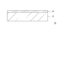
- FIG. 1 is a cross-sectional view of a transparent conductive layer forming substrate according to the first embodiment of the present invention.
- a substrate 10 for forming a transparent conductive layer according to the first embodiment of the present invention includes a substrate film 12, a first resin layer 14 formed on the surface of the substrate film 12, Have.
- the first resin layer 14 is in contact with the base film 12.
- the first resin layer 14 is provided only on one surface of the base film 12.
- the base film 12 is not particularly limited as long as it has transparency.
- Examples of the base film 12 include transparent polymer films and glass films.
- the transparency means that the total light transmittance in the visible light wavelength region is 50% or more, and the total light transmittance is more preferably 85% or more.
- the total light transmittance can be measured according to JIS K7361-1 (1997).
- the thickness of the base film 12 is not particularly limited, but is preferably in the range of 2 to 500 ⁇ m from the viewpoint of excellent handleability. More preferably, it is in the range of 2 to 200 ⁇ m.
- the "film” generally means a film having a thickness of less than 0.25 mm, but a film having a thickness of 0.25 mm or more has a thickness of 0 if it can be wound into a roll. Even if it is 0.25 mm or more, it is included in the "film”.
- polymer material of the base film 12 examples include polyester resins such as polyethylene terephthalate resin and polyethylene naphthalate resin, polycarbonate resin, poly(meth)acrylate resin, polystyrene resin, polyamide resin, polyimide resin, polyacrylonitrile resin, polypropylene resin, Polyolefin resin such as polyethylene resin, polycycloolefin resin, cycloolefin copolymer resin, polyphenylene sulfide resin, polyvinyl chloride resin, polyvinylidene chloride resin, polyvinyl alcohol resin and the like can be mentioned.
- the polymer material of the base film 12 may be composed of only one of these, or may be composed of a combination of two or more thereof.
- polyethylene terephthalate resin, polyimide resin, polycarbonate resin, poly(meth)acrylate resin, polycycloolefin resin, and cycloolefin copolymer resin are more preferable from the viewpoint of optical characteristics and durability.
- the base film 12 may be composed of a single layer composed of a layer containing one or more of the above polymeric materials, or a layer containing one or more of the above polymeric materials, and It may be composed of two or more layers such as a layer containing one kind or two or more kinds of polymer materials different from the layers.
- the first resin layer 14 is made of a cured product of a curable composition containing an ultraviolet curable resin having a silsesquioxane skeleton. Since the first resin layer 14 contains the compound having a silsesquioxane skeleton, the adhesiveness of the transparent conductive layer to be laminated is excellent. Moreover, since the compound having a silsesquioxane skeleton is an ultraviolet curable resin, the first resin layer 14 has excellent scratch resistance.
- the ultraviolet curable resin having a silsesquioxane skeleton has a structure represented by the following formula (1). (Chemical formula 1) (R-SiO 1.5 )n (1)
- n is an integer of 2 or more.
- R is an organic group, and at least a part of the plurality of Rs is a UV-reactive reactive group.
- the UV-reactive reactive group include radically polymerizable reactive groups having an ethylenically unsaturated bond such as acryloyl group, methacryloyl group, allyl group and vinyl group, and cationic polymerizable type reactive groups such as oxetanyl group. Is mentioned.
- an acryloyl group, a methacryloyl group, and an oxetanyl group are more preferable, and an acryloyl group and a methacryloyl group are particularly preferable because they are excellent in weather resistance and optical transparency. That is, (meth)acrylate having a silsesquioxane skeleton is particularly preferable.
- (meth)acrylate means “at least one of acrylate and methacrylate”.
- (Meth)acryloyl” means “at least one of acryloyl and methacryloyl”.
- “(Meth)acrylic” means “at least one of acrylic and methacrylic”.
- the functional group equivalent of the UV curable resin having a silsesquioxane skeleton is preferably within the range of 80 to 10,000 g/eq. It is more preferably within the range of 100 to 1000 g/eq, and even more preferably within the range of 150 to 300 g/eq. When the functional group equivalent is in this range, the UV curability is excellent.
- the functional group equivalent represents the mass (g) per equivalent of the functional group. Further, the functional group refers to a UV reactive group.
- the ultraviolet curable resin having a silsesquioxane skeleton preferably contains a hydroxyl group or an alkoxy group in the silsesquioxane skeleton before or after curing.
- a hydroxyl group or an alkoxy group By containing a hydroxyl group or an alkoxy group, the adhesiveness of the transparent conductive layer to be laminated is improved.
- the silsesquioxane has a complete cage structure, a ladder structure, a random structure, an incomplete cage structure, and the like.
- the complete cage type structure and the ladder type structure do not include a hydroxyl group and an alkoxy group, but the random structure and the incomplete cage type structure include a hydroxyl group and an alkoxy group. Therefore, it is preferable that part or all of the silsesquioxane skeleton has a random structure or an incomplete cage structure.
- the UV curable resin having a silsesquioxane skeleton is AC-SQ TA-100, MAC-SQ TM-100, AC-SQ SI-20, MAC-SQ SI-20, MAC-SQ HDM manufactured by Toagosei. , OX-SQ TX-100, OX-SQ SI-20, OX-SQ HDX, etc.
- the curable composition forming the first resin layer 14 may include an ultraviolet curable resin having no silsesquioxane skeleton in addition to the ultraviolet curable resin having a silsesquioxane skeleton. However, it may not be included. Further, the non-ultraviolet curable resin may or may not be contained. Moreover, the curable composition forming the first resin layer 14 may include a photopolymerization initiator. Moreover, the additive etc. which are added to a curable composition may be contained as needed.
- additives examples include a dispersant, a leveling agent, an antifoaming agent, a thixotropic agent, an antifouling agent, an antibacterial agent, a flame retardant, a slip agent, inorganic particles, and resin particles. Further, a solvent may be contained if necessary.
- the content of the ultraviolet curable resin having a silsesquioxane skeleton is 0.5% by mass or more based on the total solid content of the curable composition. Is preferred. It is more preferably 2% by mass or more, and further preferably 4% by mass or more.
- the solid content of the curable composition is a component excluding the solvent. When the content is 1% by mass or more, the adhesion of the transparent conductive layer to be laminated is more excellent.
- the content of the ultraviolet curable resin having a silsesquioxane skeleton may be 100% by mass based on the total solid content of the curable composition. It is preferably 98% by mass or less. When the content is within the above range, the transparent conductive layer can be excellent in adhesion and scratch resistance.
- Examples of the ultraviolet curable resin having no silsesquioxane skeleton include monomers, oligomers and prepolymers having a reactive group reactive with ultraviolet rays and having no silsesquioxane skeleton.
- Examples of the UV-reactive reactive group include radically polymerizable reactive groups having an ethylenically unsaturated bond such as acryloyl group, methacryloyl group, allyl group and vinyl group, and cationic polymerizable type reactive groups such as oxetanyl group. Is mentioned.
- an acryloyl group, a methacryloyl group and an oxetanyl group are more preferable, and an acryloyl group and a methacryloyl group are particularly preferable. That is, a (meth)acrylate having no silsesquioxane skeleton is particularly preferable.
- urethane (meth)acrylate As the (meth)acrylate having no silsesquioxane skeleton, urethane (meth)acrylate, silicone (meth)acrylate, alkyl (meth)acrylate, aryl (meth) having no silsesquioxane skeleton Examples thereof include acrylate. Among these, urethane (meth)acrylate is particularly preferable from the viewpoint of excellent flexibility.
- non-ultraviolet curable resins examples include thermoplastic resins and thermosetting resins.
- thermoplastic resin examples include polyester resin, polyether resin, polyolefin resin, and polyamide resin.
- thermosetting resins examples include unsaturated polyester resins, epoxy resins, alkyd resins, and phenol resins.
- Examples of the photopolymerization initiator include alkylphenone-based, acylphosphine oxide-based, and oxime ester-based photopolymerization initiators.
- Examples of the alkylphenone photopolymerization initiator include 2,2′-dimethoxy-1,2-diphenylethan-1-one, 1-hydroxy-cyclohexyl-phenyl-ketone, 2-hydroxy-2-methyl-1-phenyl- Propan-1-one, 1-[4-(2-hydroxyethoxy)-phenyl]-2-hydroxy-2-methyl-1-propan-1-one, 2-hydroxy-1- ⁇ 4-[4-( 2-hydroxy-2-methyl-propionyl)-benzyl]phenyl ⁇ -2-methyl-propan-1-one, 2-methyl-1-[4-(methylthio)phenyl]-2-morpholinopropan-1-one, 2-benzylmethyl-2-(dimethylamino)-1-(4-morpholinophenyl)-1-butanone, 2-(dimethyl
- acylphosphine oxide photopolymerization initiator examples include 2,4,6-trimethylbenzoyldiphenylphosphine oxide, bis(2,4,6-trimethylbenzoyl)-phenylphosphine oxide, and bis(2,6-dimethoxybenzoyl)-2. , 4,4-trimethyl-pentylphosphine oxide and the like.
- oxime ester photopolymerization initiator examples include 1,2-octanedione, 1-[4-(phenylthio)phenyl]-2-(O-benzoyloxime), and ethanone-1-[9-ethyl-6-(2- Methylbenzoyl)-9H-carbazol-3-yl]-1-(O-acetyloxime) and the like. These photopolymerization initiators may be used alone or in combination of two or more.
- the content of the photopolymerization initiator is preferably in the range of 0.1 to 10 mass% based on the total solid content of the curable composition. It is more preferably in the range of 1 to 5% by mass.
- the inorganic particles are added, for example, for the purpose of forming surface irregularities on the first resin layer 14 or adjusting the first resin layer 14 to have a high refractive index.
- the resin particles are added for the purpose of forming surface irregularities on the first resin layer 14, for example.
- the high refractive index means a refractive index at a measurement wavelength of 589.3 nm of 1.50 or more, preferably in the range of 1.55 to 1.80, and more preferably in the range of 1.60 to 1.70. ..
- Inorganic particles capable of optically adjusting the first resin layer 14 to a high refractive index include oxides of metals such as titanium, zirconium, tin, zinc, silicon, niobium, aluminum, chromium, magnesium, germanium, gallium, antimony and platinum.
- metal oxide particles are: These may be used alone as the optically adjustable inorganic particles, or may be used in combination of two or more kinds.
- titanium oxide and zirconium oxide are particularly preferable from the viewpoint of excellent compatibility between high refractive index and transparency.
- the types of inorganic particles and resin particles that form surface irregularities on the first resin layer 14 are not particularly limited.
- examples of such inorganic particles include metal oxide particles made of oxides of metals such as titanium, zirconium, silicon, aluminum and calcium.
- examples of such resin particles include (meth)acrylic resin, styrene resin, styrene-(meth)acrylic resin, urethane resin, polyamide resin, silicone resin, epoxy resin, phenol resin, polyethylene resin, and cellulose.
- the resin particles include a resin.
- the average particle diameter of the inorganic particles or the resin particles is equal to or larger than the thickness of the first resin layer 14. More preferably 1.1 times or more and 20 times or less the thickness of the first resin layer 14, further preferably 1.5 times or more and 10 times or less the thickness of the first resin layer 14, and particularly preferably the thickness of the first resin layer 14. Is 1.5 times or more and 5 times or less.
- the average particle diameter is a volume-based average arithmetic value obtained by a laser diffraction/scattering method according to JIS Z8825.
- the thickness of the first resin layer 14 is not particularly limited, but is preferably 0.005 ⁇ m or more from the viewpoint of excellent film continuity.
- the thickness is more preferably 0.010 ⁇ m or more, still more preferably 0.020 ⁇ m or more.
- the thickness of the first resin layer 14 is preferably 10 ⁇ m or less from the viewpoint of easily curling curl due to the difference in heat shrinkage with the base film 12. It is more preferably 5 ⁇ m or less, still more preferably 1 ⁇ m or less.
- the thickness of the first resin layer 14 is the thickness of a relatively smooth portion in a portion where no inorganic particles or resin particles are present in the thickness direction.
- the arithmetic average roughness Ra of the surface of the first resin layer 14 on which the surface irregularities are formed is 0.1 to 130 nm from the viewpoint of easily preventing blocking of adhesion between the front surface and the back surface of the transparent conductive layer forming substrate. It is preferably within the range. It is more preferably within the range of 0.5 to 50 nm, still more preferably within the range of 2 to 20 nm.
- the range of the average particle diameter, in the range of the average arithmetic roughness, the distribution density of the inorganic particles and resin particles It is preferably in the range of 100 to 2000 pieces/mm 2 . More preferably, it is in the range of 100 to 1000 pieces/mm 2 .
- alcohol solvents such as ethylene glycol monomethyl ether (EGM), propylene glycol monomethyl ether (PGM) and diethylene glycol monobutyl ether, methyl ethyl ketone (MEK), methyl isobutyl ketone (MIBK), cyclohexanone , Ketones such as acetone, aromatic solvents such as toluene and xylene, amide solvents such as N-methylpyrrolidone, acetamide and dimethylformamide. These may be used alone as a solvent, or may be used in combination of two or more kinds.
- ECM ethylene glycol monomethyl ether
- PGM propylene glycol monomethyl ether
- MEK methyl ethyl ketone
- MIBK methyl isobutyl ketone
- Ketones such as acetone
- aromatic solvents such as toluene and xylene
- amide solvents such as N-methylpyrrolidone
- the solid content concentration (concentration of components other than the solvent) of the curable composition may be appropriately determined in consideration of coatability and film thickness. For example, it may be 1 to 90% by mass, 1.5 to 80% by mass, 2 to 70% by mass, and the like.
- the transparent conductive layer-forming substrate 10 is produced by applying a curable composition for forming the first resin layer 14 onto the surface of the substrate film 12, drying it if necessary, and then curing it by irradiating it with ultraviolet rays. can do.
- the surface of the base film 12 may be subjected to a surface treatment before coating. Examples of the surface treatment include corona treatment, plasma treatment, hot air treatment, ozone treatment, and ultraviolet treatment.
- reverse gravure coating method for example, reverse gravure coating method, direct gravure coating method, die coating method, bar coating method, wire bar coating method, roll coating method, spin coating method, dip coating method, spray coating method, knife coating method, kiss coating method.
- various printing methods such as inkjet printing, offset printing, screen printing, and flexo printing.
- the drying step is not particularly limited as long as the solvent used in the coating liquid can be removed, but it is preferably performed at a temperature of 50 to 150° C. for about 10 to 180 seconds. Particularly, the drying temperature is preferably 50 to 120°C.
- a high-pressure mercury lamp, an electrodeless (microwave system) lamp, a xenon lamp, a metal halide lamp, or any other ultraviolet irradiation device can be used for ultraviolet irradiation.
- the ultraviolet irradiation may be performed under an atmosphere of an inert gas such as nitrogen, if necessary.
- UV irradiation dose but it is not limited to, preferably 50 ⁇ 800mJ / cm 2, more preferably 100 ⁇ 300mJ / cm 2.
- the curable composition in which the first resin layer 14 formed on the surface of the base material film 12 contains an ultraviolet curable resin having a silsesquioxane skeleton Since it is composed of the cured product of (1), it has excellent adhesion to the transparent conductive layer to be laminated and excellent scratch resistance.
- the transparent conductive layer forming base material according to the present invention is not limited to the configuration of the transparent conductive layer forming base material 10 according to the first embodiment. Another embodiment of the transparent conductive layer forming substrate according to the present invention will be described below.
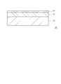
- FIG. 2 shows a transparent conductive layer forming substrate 20 according to the second embodiment.
- the transparent conductive layer forming base material 20 according to the second embodiment is formed on the base film 12, the second resin layer 16 formed on the surface of the base film 12, and the surface of the second resin layer 16.
- the first resin layer 14 is formed.
- the second resin layer 16 is in contact with the base film 12, and the first resin layer 14 is in contact with the second resin layer 16.
- the first resin layer 14 is provided only on one surface of the base film 12.
- the transparent conductive layer forming substrate 20 has a substrate film 12, a second resin layer 16 and a first resin layer 14 in this order from the side of the substrate film 12.
- the transparent conductive layer forming base material 20 according to the second embodiment has a second gap between the base film 12 and the first resin layer 14 as compared with the transparent conductive layer forming base material 10 according to the first embodiment. Except for this point, the resin layer 16 is provided, and the other points are the same as those of the transparent conductive layer forming substrate 10 according to the first embodiment, and the description of the same configuration is omitted.
- the second resin layer 16 is disposed between the base film 12 and the first resin layer 14, and is composed of a cured product of a curable composition containing an ultraviolet curable resin having no silsesquioxane skeleton. ..
- the curable composition for forming the second resin layer 16 does not include an ultraviolet curable resin having a silsesquioxane skeleton.
- Examples of the ultraviolet curable resin having no silsesquioxane skeleton include monomers, oligomers and prepolymers having a reactive group reactive with ultraviolet rays and having no silsesquioxane skeleton.
- Examples of the UV-reactive reactive group include radically polymerizable reactive groups having an ethylenically unsaturated bond such as acryloyl group, methacryloyl group, allyl group and vinyl group, and cationic polymerizable type reactive groups such as oxetanyl group. Is mentioned.
- an acryloyl group, a methacryloyl group and an oxetanyl group are more preferable, and an acryloyl group and a methacryloyl group are particularly preferable. That is, a (meth)acrylate having no silsesquioxane skeleton is particularly preferable.
- urethane (meth)acrylate As the (meth)acrylate having no silsesquioxane skeleton, urethane (meth)acrylate, silicone (meth)acrylate, alkyl (meth)acrylate, aryl (meth) having no silsesquioxane skeleton Examples thereof include acrylate. Among these, urethane (meth)acrylate is particularly preferable from the viewpoint of excellent flexibility.
- the curable composition for forming the second resin layer 16 contains urethane (meth)acrylate as the ultraviolet curable resin, for example, the base film 12 is formed of polycycloolefin, cycloolefin copolymer, or the like. Even if the target film is easily cracked, it is easy to suppress cracking of the base film 12.
- the second resin layer 16 is preferably a hard coat layer. From this viewpoint, the pencil hardness is preferably in the range of 2B to 6H. The pencil hardness can be measured according to JIS K5600-5-4. The second resin layer 16 is formed of a composition containing an ultraviolet curable resin, so that the above pencil hardness is easily satisfied.
- the curable composition forming the second resin layer 16 may or may not contain a non-ultraviolet curable resin in addition to the ultraviolet curable resin having no silsesquioxane skeleton. May be. Moreover, the curable composition forming the second resin layer 16 may include a photopolymerization initiator. Moreover, the additive etc. which are added to a curable composition may be contained as needed. Examples of such additives include a dispersant, a leveling agent, an antifoaming agent, a thixotropic agent, an antifouling agent, an antibacterial agent, a flame retardant, a slip agent, inorganic particles, and resin particles. Further, a solvent may be contained if necessary. The non-ultraviolet curable resin, the photopolymerization initiator, and the solvent can be appropriately selected from those described in the curable composition forming the first resin layer 14.
- the inorganic particles are added, for example, for the purpose of forming surface irregularities on the first resin layer 14 or adjusting the second resin layer 16 to have a high refractive index.
- the resin particles are added for the purpose of forming surface irregularities on the first resin layer 14, for example.
- the high refractive index means a refractive index at a measurement wavelength of 589.3 nm of 1.50 or more, preferably in the range of 1.55 to 1.80, and more preferably in the range of 1.60 to 1.70. ..
- the low refractive index means a refractive index at a measurement wavelength of 589.3 nm of less than 1.50, preferably in the range of 1.30 to 1.50, and more preferably in the range of 1.40 to 1.50. ..
- Examples of the inorganic particles capable of optically adjusting the second resin layer 16 to a high refractive index include oxides of metals such as titanium, zirconium, tin, zinc, silicon, niobium, aluminum, chromium, magnesium, germanium, gallium, antimony and platinum.
- Examples of the metal oxide particles are: These may be used alone as the optically adjustable inorganic particles, or may be used in combination of two or more kinds. Among these, titanium oxide and zirconium oxide are particularly preferable from the viewpoint of excellent compatibility between high refractive index and transparency.
- examples of the inorganic particles capable of optically adjusting the first resin layer 14 to a low refractive index include particles of magnesium fluoride, silica, silsesquioxane, calcium fluoride and the like. It is more preferable that these particles have a hollow structure from the viewpoint of easily achieving a low refractive index.
- the type of inorganic particles or resin particles that are particles added to the curable composition that forms the second resin layer 16 and that form surface irregularities on the first resin layer 14 is the curability that forms the first resin layer 14. It can be appropriately selected from those described in the composition.
- the solid content concentration of the curable composition can be adjusted in the same manner as the curable composition forming the first resin layer 14.
- the average particle diameter of the inorganic particles and the resin particles is equal to or larger than the total thickness of the first resin layer 14 and the second resin layer 16. More preferably 1.1 times or more and 20 times or less of the total thickness of the first resin layer 14 and the second resin layer 16, and even more preferably 1.5 times the total thickness of the first resin layer 14 and the second resin layer 16. It is not less than 10 times and not more than 10 times, particularly preferably not less than 1.5 times and not more than 5 times the total thickness of the first resin layer 14 and the second resin layer 16.
- the thickness of the second resin layer 16 is not particularly limited, but it is preferably 0.005 ⁇ m or more from the viewpoint of excellent film continuity.
- the thickness is more preferably 0.010 ⁇ m or more, still more preferably 0.10 ⁇ m or more.
- the thickness of the second resin layer 16 is preferably 10 ⁇ m or less from the viewpoint that curling due to the difference in heat shrinkage with the base film 12 is easily suppressed. It is more preferably 5 ⁇ m or less, still more preferably 1 ⁇ m or less.
- the total thickness of the first resin layer 14 and the second resin layer 16 is preferably 10 ⁇ m or less.
- the thickness of the second resin layer 16 is the thickness of a relatively smooth portion in a portion where no inorganic particles or resin particles are present in the thickness direction.
- the arithmetic average roughness Ra of the surface of the first resin layer 14 on which the surface irregularities are formed is preferably in the range of 0.1 to 130 nm from the viewpoint of blocking and the like. It is more preferably within the range of 0.5 to 50 nm, still more preferably within the range of 2 to 20 nm.
- the distribution density of the inorganic particles and resin particles Is preferably in the range of 100 to 2000 pieces/mm 2 . More preferably, it is in the range of 100 to 1000 pieces/mm 2 .
- the transparent conductive layer forming base material 20 is obtained by applying a curable composition for forming the second resin layer 16 on the surface of the base material film 12, drying it if necessary, and then curing it by irradiating with ultraviolet rays to obtain a base material.
- a curable composition for forming the first resin layer 14 is applied on the surface of the second resin layer 16 and, if necessary, after drying. It can be manufactured by curing the resin by ultraviolet irradiation and forming the first resin layer 14 on the surface of the second resin layer 16.
- the surface of the base film 12 may be subjected to a surface treatment before coating. Examples of the surface treatment include corona treatment, plasma treatment, hot air treatment, ozone treatment, and ultraviolet treatment.
- the curable composition in which the first resin layer 14 formed on the surface of the base material film 12 contains an ultraviolet curable resin having a silsesquioxane skeleton Since it is composed of the cured product of (1), it has excellent adhesion to the transparent conductive layer to be laminated and excellent scratch resistance. Further, since the second resin layer 16 made of a cured product of a curable composition containing an ultraviolet curable resin having no silsesquioxane skeleton is provided between the base film 12 and the first resin layer 14. , It becomes easy to design the optical adjustment function and the blocking prevention function.
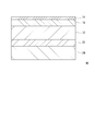
- FIG. 3 shows a transparent conductive layer forming substrate 30 according to the third embodiment.
- the transparent conductive layer forming base material 30 according to the third embodiment includes a base film 12, a second resin layer 16 formed on one surface of the base film 12, and a surface of the second resin layer 16. And a third resin layer 18 formed on the other surface of the base film 12.
- the second resin layer 16 is in contact with one surface of the base film 12, and the first resin layer 14 is in contact with the second resin layer 16.
- the third resin layer 18 is in contact with the other surface of the base film 12.
- the first resin layer 14 is provided only on one surface of the base film 12.
- the transparent conductive layer forming substrate has a third resin layer 18, a substrate film 12, a second resin layer 16 and a first resin layer 14 in this order from the third resin layer 18 side.
- the transparent conductive layer forming base material 30 according to the third embodiment is different from the transparent conductive layer forming base material 20 according to the second embodiment in that the third resin layer 18 is provided on the other surface of the base material film 12. Other than that, it is the same as the transparent conductive layer forming substrate 20 according to the second embodiment except the above, and the description of the same configuration will be omitted.
- the third resin layer 18 is made of a cured product of a curable composition containing an ultraviolet curable resin having no silsesquioxane skeleton.
- the curable composition forming the third resin layer 18 can be the same composition as the curable composition forming the second resin layer 16.
- the third resin layer 18 is preferably a hard coat layer. From this viewpoint, the pencil hardness is preferably in the range of 2B to 6H. The pencil hardness can be measured according to JIS K5600-5-4. The third resin layer 18 is formed of a composition containing an ultraviolet curable resin, so that the above pencil hardness is easily satisfied.
- the thickness of the third resin layer 18 is not particularly limited and can be the same as the thickness of the second resin layer 16.
- the thickness of the third resin layer 18 is close to the thickness of the second resin layer 16 or the total thickness of the second resin layer 16 and the first resin layer 14 (for example, within ⁇ 10%), at the time of curing It is easy to suppress curl due to shrinkage.
- the transparent conductive layer forming base material 30 is obtained by applying a curable composition for forming the second resin layer 16 on one surface of the base material film 12, drying it if necessary, and then curing it by ultraviolet irradiation. After forming the second resin layer 16 on one surface of the base material film 12, a curable composition for forming the first resin layer 14 is applied on the surface of the second resin layer 16 and, if necessary, Accordingly, after drying, it is cured by irradiation with ultraviolet rays to form the first resin layer 14 on the surface of the second resin layer 16 and the third resin layer 18 on the other surface of the base film 12.
- the surface of the base film 12 before the coating is applied.
- Treatment may be applied. Examples of the surface treatment include corona treatment, plasma treatment, hot air treatment, ozone treatment, and ultraviolet treatment.
- the first resin layer 14 formed on one surface of the base material film 12 has curability including an ultraviolet curable resin having a silsesquioxane skeleton. Since it is a cured product of the composition, it has excellent adhesion to the transparent conductive layer to be laminated and excellent scratch resistance. Further, since the second resin layer 16 made of a cured product of a curable composition containing an ultraviolet curable resin having no silsesquioxane skeleton is provided between the base film 12 and the first resin layer 14. , It becomes easy to design the optical adjustment function and the blocking prevention function.
- the third resin layer 18 made of a cured product of a curable composition containing an ultraviolet curable resin having no silsesquioxane skeleton is formed on the other surface of the base film 12,
- the other surface side of the base film 12 also has excellent scratch resistance.
- FIG. 4 shows a transparent conductive layer forming substrate 40 according to the fourth embodiment.
- the transparent conductive layer forming base material 40 according to the fourth embodiment includes a base film 12, a second resin layer 16 formed on one surface of the base film 12, and a surface of the second resin layer 16.
- the first resin layer 14 formed on the base film 12, and the protective film 24 disposed on the other surface of the base film 12 via the adhesive layer 22.
- the second resin layer 16 is in contact with one surface of the base film 12, and the first resin layer 14 is in contact with the second resin layer 16.
- the protective film 24 is in contact with the other surface of the base film 12 via the adhesive layer 22.
- the first resin layer 14 is provided only on one surface of the base film 12.
- the transparent conductive layer forming substrate 40 has a protective film 24, an adhesive layer 22, a substrate film 12, a second resin layer 16, and a first resin layer 14 in this order from the protective film 24 side.
- the transparent conductive layer forming base material 40 according to the fourth embodiment has an adhesive layer 22 on the other surface of the base material film 12 as compared with the transparent conductive layer forming base material 20 according to the second embodiment.
- the other difference is that the protective film 24 is provided, and the other points are the same as those of the transparent conductive layer forming substrate 20 according to the second embodiment, and the description of the same configuration is omitted.
- the protective film 24 can prevent the other surface of the base film 12 from being scratched during handling such as continuous processing by a roll process or the like.
- the protective film 24 is attached to the other surface of the base film 12 via the adhesive layer 22.
- the protective film 24 is peeled off from the other surface of the base film 12 together with the pressure-sensitive adhesive layer 22 after processing. Therefore, in the pressure-sensitive adhesive layer 22, the adhesive force between the protective film 24 and the pressure-sensitive adhesive layer 22 is stronger than the adhesive force between the base film 12 and the pressure-sensitive adhesive layer 22, and the base film 12 and the pressure-sensitive adhesive layer 22.
- the adhesive strength between 22 is adjusted so that the interface can be peeled off.
- the material forming the protective film 24 As the material forming the protective film 24, those exemplified as the material forming the base film 12 can be appropriately selected.
- the material forming the protective film 24 is not particularly limited, but a material having a heat shrinkage ratio or a linear expansion coefficient close to that of the base film 12 is preferable from the viewpoint of excellent curl suppression by heat treatment.
- the material is the same as or the same as the material of the base film 12.
- the same kind can indicate, for example, polyesters, poly(meth)acrylates, polyamides, and the like.
- the thickness of the protective film 24 is not particularly limited, but may be, for example, approximately the same as the thickness of the base film 12 so that the heat shrinkage ratio and the linear expansion coefficient of the base film 12 are close to each other. Specifically, for example, it may be in the range of 2 to 500 ⁇ m and in the range of 2 to 200 ⁇ m.
- the pressure-sensitive adhesive forming the pressure-sensitive adhesive layer 22 is not particularly limited, and an acrylic pressure-sensitive adhesive, a silicone pressure-sensitive adhesive, a urethane pressure-sensitive adhesive or the like can be preferably used.
- an acrylic pressure-sensitive adhesive is preferable because it has excellent transparency and heat resistance.
- the acrylic pressure-sensitive adhesive is preferably formed from a pressure-sensitive adhesive composition containing a (meth)acrylic polymer and a crosslinking agent.
- (Meth)acrylic polymer is a homopolymer or copolymer of (meth)acrylic monomer.
- the (meth)acrylic monomer include an alkyl group-containing (meth)acrylic monomer, a carboxyl group-containing (meth)acrylic monomer, and a hydroxyl group-containing (meth)acrylic monomer.
- alkyl group-containing (meth)acrylic monomer examples include (meth)acrylic monomers having an alkyl group having 2 to 30 carbon atoms.
- the alkyl group having 2 to 30 carbon atoms may be linear, branched, or cyclic.
- Specific examples of the alkyl group-containing (meth)acrylic monomer include, for example, isostearyl (meth)acrylate, stearyl (meth)acrylate, lauryl (meth)acrylate, dodecyl (meth)acrylate, and (meth)acrylate.
- Decyl acrylate isononyl (meth)acrylate, nonyl (meth)acrylate, isooctyl (meth)acrylate, octyl (meth)acrylate, isobutyl (meth)acrylate, n-butyl (meth)acrylate, ( Pentyl (meth)acrylate, hexyl (meth)acrylate, cyclohexyl (meth)acrylate, 2-ethylhexyl (meth)acrylate, propyl (meth)acrylate, ethyl (meth)acrylate, methyl (meth)acrylate, etc. Is mentioned.
- Examples of the carboxyl group-containing (meth)acrylic monomer include (meth)acrylic acid, carboxyethyl (meth)acrylate, and carboxypentyl (meth)acrylate.
- the carboxyl group may be located at the end of the alkyl chain or in the middle of the alkyl chain.
- hydroxyl group-containing (meth)acrylic monomer examples include hydroxylauryl (meth)acrylate, hydroxydecyl (meth)acrylate, hydroxyoctyl (meth)acrylate, hydroxyhexyl (meth)acrylate, hydroxybutyl (meth)acrylate, Examples thereof include hydroxypropyl (meth)acrylate and hydroxyethyl (meth)acrylate.
- the hydroxyl group may be located at the end of the alkyl chain or may be located in the middle of the alkyl chain.
- the (meth)acrylic monomer forming the (meth)acrylic polymer may be any one of the above, or a combination of two or more thereof.
- crosslinking agent examples include an isocyanate crosslinking agent, an epoxy crosslinking agent, a metal chelate crosslinking agent, a metal alkoxide crosslinking agent, a carbodiimide crosslinking agent, an oxazoline crosslinking agent, an aziridine crosslinking agent, and a melamine crosslinking agent. ..
- the cross-linking agent one type of these may be used alone, or two or more types may be used in combination.
- the adhesive composition may contain other additives in addition to the (meth)acrylic polymer and the crosslinking agent.
- additives include cross-linking accelerators, cross-linking retarders, tackifying resins (tackifiers), antistatic agents, silane coupling agents, plasticizers, release aids, pigments, dyes, wetting agents, thickeners. , Ultraviolet absorbers, antiseptics, antioxidants, metal deactivators, alkylating agents, flame retardants and the like. These are appropriately selected and used according to the application and purpose of use of the pressure-sensitive adhesive.
- the thickness of the adhesive layer 22 is not particularly limited, but is preferably in the range of 1 to 10 ⁇ m. More preferably, it is in the range of 2 to 7 ⁇ m.
- FIG. 5 shows a transparent conductive layer forming substrate 50 according to the fifth embodiment.
- the second resin layer 16 is formed on both surfaces of the substrate film 12, and the first resin is formed on each of the surfaces of the second resin layers 16.
- the layer 14 is formed.
- the second resin layer 16 is in contact with the base film 12, and the first resin layer 14 is in contact with the second resin layer 16.
- the transparent conductive layer forming substrate 50 has a first resin layer 14, a second resin layer 16, a substrate film 12, a second resin layer 16 and a first resin layer 14 in this order from the first resin layer 14 side. ing.
- the second resin layer 16 and the first resin layer 14 are base material films as compared with the transparent conductive layer forming base material 20 according to the second embodiment. 12 is the same as that of the transparent conductive layer forming base material 20 according to the second embodiment, and the description thereof is omitted.
- the transparent conductive layer forming substrate 50 has the first resin layer 14 on both sides of the substrate film 12, and thus forms a transparent conductive film having a transparent conductive layer on both sides of the substrate film 12. Is suitable as
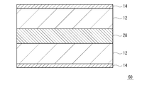
- FIG. 6 shows a transparent conductive layer forming substrate 60 according to the sixth embodiment.
- the transparent conductive layer forming base material 60 according to the sixth embodiment two transparent conductive layer forming base materials 10 shown in FIG. 1 are used, and the base material film 12 sides thereof are bonded to each other via the adhesive layer 28. It is composed of
- the transparent conductive layer forming substrate 60 has a first resin layer 14, a substrate film 12, an adhesive layer 28, a substrate film 12, and a first resin layer 14 in that order.
- the transparent conductive layer forming base material 60 Since the transparent conductive layer forming base material 60 has the first resin layer 14 on both sides, it is a base for forming a transparent conductive film having a structure having transparent conductive layers on both sides, like the transparent conductive layer forming base material 50. It is suitable as a material.
- the transparent conductive layer forming base material 60 uses two transparent conductive layer forming base materials 10 shown in FIG. 1, and since it has two base material films 12, it is unlikely to break in the transparent conductive layer forming step. Excellent handling.
- the adhesive layer 28 is for sticking the two base material films 12 together with good adhesion. It differs from the pressure-sensitive adhesive layer 22 of the transparent conductive layer forming substrate 40 shown in FIG. 4 in that it is hard to peel off.
- the pressure-sensitive adhesive (pressure-sensitive adhesive composition) forming the pressure-sensitive adhesive layer 28 the pressure-sensitive adhesive (pressure-sensitive adhesive composition) in the transparent conductive layer forming substrate 70 according to the seventh embodiment described later can be preferably used.
- the thickness of the adhesive layer 28 is not particularly limited, but is preferably in the range of 5 to 100 ⁇ m. More preferably, it is in the range of 10 to 50 ⁇ m.
- the pressure-sensitive adhesive layer 28 is formed by directly coating the pressure-sensitive adhesive composition on the other surface of the base film 12, or by coating the pressure-sensitive adhesive composition on the surface of the release film and then forming the base material.
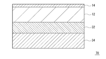
- FIG. 7 shows a transparent conductive layer forming base material 70 according to the seventh embodiment.
- the transparent conductive layer forming base material 70 according to the seventh embodiment includes a base film 12, a first resin layer 14 formed on one surface of the base film 12, and the other surface of the base film 12.
- the pressure-sensitive adhesive layer 32 formed on the top and the release film 34 formed on the surface of the pressure-sensitive adhesive layer 32 are included.
- the first resin layer 14 is in contact with one surface of the base film 12, and the adhesive layer 32 is in contact with the other surface of the base film 12.
- the first resin layer 14 is provided only on one surface of the base film 12.
- the transparent conductive layer forming substrate 70 has a release film 34, an adhesive layer 32, a substrate film 12, and a first resin layer 14 in this order from the release film 34 side.
- the transparent conductive layer forming base material 70 according to the seventh embodiment has an adhesive layer 32 on the other surface of the base film 12 as compared with the transparent conductive layer forming base material 10 according to the first embodiment. Except for this, the release film 34 is provided, and other than this, the substrate is the same as the transparent conductive layer forming substrate 10 according to the first embodiment, and the description of the same configuration is omitted.
- the adhesive layer 32 is for sticking the transparent conductive layer forming base material 70 to a substrate such as a polymer film or glass with good adhesion.
- the pressure-sensitive adhesive composition forming the pressure-sensitive adhesive layer 32 can contain a known pressure-sensitive adhesive resin such as an acrylic pressure-sensitive adhesive, a silicone pressure-sensitive adhesive, a urethane pressure-sensitive adhesive. Among them, acrylic adhesives are preferable from the viewpoint of optical transparency and heat resistance.
- the pressure-sensitive adhesive composition preferably contains a crosslinking agent in order to enhance the cohesive force of the pressure-sensitive adhesive layer 32. Examples of the crosslinking agent include an isocyanate crosslinking agent, an epoxy crosslinking agent, an aziridine crosslinking agent, and a chelate crosslinking agent.
- the pressure-sensitive adhesive composition may contain additives, if necessary.
- the additive include known additives such as a plasticizer, a silane coupling agent, a surfactant, an antioxidant, a filler, a curing accelerator and a curing retarder.
- you may dilute using an organic solvent from a viewpoint of productivity.
- the thickness of the adhesive layer 32 is not particularly limited, but is preferably in the range of 5 to 100 ⁇ m. More preferably, it is in the range of 10 to 50 ⁇ m.
- the pressure-sensitive adhesive layer 32 is formed by directly coating the pressure-sensitive adhesive composition on the other surface of the base film 12, or after forming the pressure-sensitive adhesive composition on the surface of the release film 34 by coating. Method of transferring to the other surface of the material film 12, after forming by applying the pressure-sensitive adhesive composition on the surface of the first release film, the second release film is stuck, and either one of the release films is released. It can be formed by a method of peeling off the mold film and transferring it onto the other surface of the base film 12.
- the adhesive layer 32 preferably has an adhesive force to glass of 4 N/25 mm or more. It is more preferably 6 N/25 mm or more, still more preferably 10 N/25 mm or more.
- the release film 34 functions as a protective layer of the adhesive layer 32 before use, and is peeled off from the adhesive layer 32 during use.
- the release film 34 is not particularly limited, and the same material as the material used for the base film 12 can be used.
- the surface of the release film 34 that contacts the adhesive layer 32 may be subjected to a release treatment.
- the release agent used in the release treatment include silicone-based, fluorine-based, alkyd-based, unsaturated polyester-based, polyolefin-based and wax-based release agents.
- FIG. 8 shows a transparent conductive film 80 according to an embodiment of the present invention.
- the transparent conductive film 80 according to one embodiment of the present invention has the transparent conductive layer 26 on the surface of the first resin layer 14 of the transparent conductive layer forming substrate 10.
- the transparent conductive layer forming substrate 10 is the transparent conductive layer forming substrate according to the present invention.
- the transparent conductive film 80 has the base film 12, the first resin layer 14, and the transparent conductive layer 26 in this order from the base film 12 side.
- the transparent conductive layer 26 contains a conductive substance.
- the conductive substance is not particularly limited, but zinc oxide, barium oxide, indium tin oxide, indium zinc oxide, zirconium oxide, ytterbium oxide, yttrium oxide, tantalum oxide, aluminum oxide, cerium oxide, titanium oxide, etc. A metal oxide is mentioned. Of these, indium tin oxide and indium zinc oxide are particularly preferable from the viewpoint of achieving both high transparency and high conductivity.
- the thickness of the transparent conductive layer 26 is not particularly limited, but is preferably in the range of 10 to 40 nm. More preferably, it is within the range of 15 to 30 nm.
- the transparent conductive layer 26 may be formed by a sputtering method, a vacuum deposition method, a CVD method, an ion plating method, or the like.
- the sputtering method is preferable from the viewpoint that a low resistance and homogeneous film can be stably produced.
- the transparent conductive layer 26 preferably has a step of firing the conductive substance after film formation in order to promote crystallization of the conductive substance.
- the firing method is not particularly limited, but for example, drum heating during sputtering, a hot air heating furnace, a far infrared heating furnace, or the like may be used.
- the heating temperature at the time of firing may be appropriately selected according to the type of conductive material. For example, the temperature may be 50 to 200° C., 80 to 180° C., 100 to 160° C., and the like.
- the heating time for firing is not particularly limited, but may be 3 to 180 minutes, 5 to 120 minutes, 10 to 90 minutes, or the like.
- the transparent conductive film 80 having the above configuration since the transparent conductive layer 26 is provided on the surface of the first resin layer 14 of the transparent conductive layer forming substrate 10 according to the present invention, The transparent conductive layer 26 has excellent adhesion. Further, since the first resin layer 14 has excellent scratch resistance, it is possible to prevent the surface of the first resin layer 14 from being scratched during handling.
- the transparent conductive film 80 according to the present invention can use the transparent conductive layer 26 as an electrode of a touch panel.
- the electrodes of the touch panel are formed by forming the transparent conductive layer 26 in a desired electrode pattern.
- the electrode pattern can be formed by etching the transparent conductive layer 26 or the like.
- the touch panel according to the present invention is configured using the transparent conductive film 80 according to the present invention, and the transparent conductive layer 26 of the transparent conductive film 80 is used as an electrode of the touch panel.
- the touch panel is a touch panel such as a capacitance type or a resistance film type.
- Examples of the touch panel according to the present invention include a GFF type touch panel and a GF2 type touch panel.
- the GFF type touch panel is, for example, as shown in FIG. 6, a transparent conductive layer formed by bonding two transparent conductive layer forming base materials 10 on the base film 12 side via an adhesive layer 28.
- a transparent adhesive a transparent conductive film 80 having one resin layer 14 and a transparent conductive layer 26, which is obtained by adhering two base film 12 sides of each other with a transparent adhesive, is used.
- One of the surfaces of the transparent conductive layer 26 is attached to a transparent base material such as glass or a resin film.
- the GF2 type touch panel is formed by a transparent conductive layer forming base material 50 having a structure in which the first resin layer 14 and the transparent conductive layer 26 are provided on both surface sides of the base film 12, as shown in FIG. 5, for example. It consists of a conductive film laminated with a transparent adhesive on a transparent substrate such as glass or resin film.
- the image display system of the touch panel according to the present invention is not particularly limited, and it can be used for any display device such as a liquid crystal display device and an organic EL display device.
- the surface of the base film 12 is subjected to a surface treatment.
- an easily adhesive layer may be provided on the surface of the base film 12.
- the surface irregularities of the first resin layer 14 are formed by adding particles having an average particle diameter larger than the thickness of the layer to which the particles are added, but the method for forming the irregularities is not limited to this. It is not something that will be done.
- the surface irregularities may be formed on a layer that forms the surface irregularities such as the first resin layer 14 by mold transfer. Further, even when particles are added to form surface irregularities, the particles are subjected to a surface treatment or combined with a surfactant to reduce the surface free energy of the particles and to add particles to the surface of the layer to which the particles are added. May be unevenly distributed to form surface irregularities due to particles.
- the average particle size of the particles may be smaller than the thickness of the layer to which the particles are added.
- the average particle size of the particles is preferably within the range of 50 to 500 nm. It is more preferably in the range of 80 to 400 nm, still more preferably in the range of 120 to 400 nm. Further, the average particle diameter is preferably 1/2 or less of the thickness of the layer to which the particles are added.
- the protective film 24 is shown as being added to the transparent conductive layer forming base material 20 of the second embodiment shown in FIG. 2, but the first embodiment shown in FIG. It may be added to the transparent conductive layer forming substrate 10. Further, it may be added to a transparent conductive film such as the transparent conductive film 80 shown in FIG.
- the pressure-sensitive adhesive layer 32 is shown as being added to the transparent conductive layer forming substrate 10 of the first embodiment shown in FIG. 1, as shown in FIG. It may be added to the conductive layer forming base materials 20 to 30. Further, it may be added to a transparent conductive film such as the transparent conductive film 80 shown in FIG.
- the sixth transparent conductive layer forming base material 60 shown in FIG. 6 is formed by laminating two transparent conductive layer forming base materials 10 on the base film 12 side with the adhesive layer 28 interposed therebetween.
- the two transparent conductive layer forming base materials 10 may be the transparent conductive layer forming base materials 20 to 30 shown in FIGS. Further, it may be a transparent conductive film such as the transparent conductive film 80 shown in FIG.
- the transparent conductive film 80 shows an example in which the transparent conductive layer forming base material 10 of the first embodiment shown in FIG. 1 is used as the transparent conductive layer forming base material.
- the transparent conductive layer forming base materials 20 to 70 shown in FIGS. 2 to 7 may be used as the transparent conductive layer forming base materials.
- various functional layers such as a gas barrier property improving layer, an antistatic layer and an oligomer block layer may be provided in advance before forming each layer.
- a curable composition for forming the first resin layer was prepared by blending each component with the blending composition (% by mass) shown in Table 1.
- curable composition for forming the second resin layer was prepared by blending the respective components with the blending composition (% by mass) shown in Table 1.
- a curable composition for forming a third resin layer was prepared by blending each component with the blending composition (% by mass) shown in Table 1.
- Example 3 (Preparation of transparent conductive layer forming substrate) (Examples 1 to 3)
- the curable composition for forming the second resin layer was applied to one surface of the base film (PET film “Lumirror UH1H” manufactured by Toray, thickness 50 ⁇ m) using a #5 wire bar, and the coating was performed at 80° C. for 1 hour.
- a second resin layer was formed by irradiating the coating film with ultraviolet rays at a light intensity of 200 mJ/cm 2 using a high pressure mercury lamp to cure the coating film with ultraviolet rays.
- the curable composition for forming the first resin layer was applied onto the surface of the second resin layer using a #4 wire bar, dried at 80° C.
- the first resin layer was formed by irradiating the coating film with ultraviolet rays at a light amount of 200 mJ/cm 2 in a nitrogen atmosphere to cure the coating film with ultraviolet rays. Then, on the other surface of the substrate film, a curable composition for forming a third resin layer was applied using a #4 wire bar and dried at 80° C. for 1 minute, and then a high pressure mercury lamp was used. The third resin layer was formed by irradiating the coating film with ultraviolet rays at a light amount of 200 mJ/cm 2 to cure the coating film with ultraviolet rays. As described above, the transparent conductive layer forming base materials according to Examples 1 to 3 were produced.
- Example 4 The base film was changed to Zeonor Film ZF16-55 (Zeonor Film ZF16-55) manufactured by Nippon Zeon Co., Ltd. (corresponding to a thickness of 55 ⁇ m), and a corona treatment was applied on one surface thereof, and then the second resin layer was not formed, and the wire bar of #5 was used.
- a transparent conductive layer-forming substrate according to Example 4 was produced in the same manner as in Example 1 except that the first resin layer was formed using. No third resin layer was formed on the other surface of the base film.
- Example 5 to 8 The base film is changed to COP film “Zeonor Film ZF16-55” (thickness 55 ⁇ m) manufactured by Nippon Zeon Co., Ltd., one side of which is subjected to corona treatment, and then a second resin layer is formed.
- Substrates for forming transparent conductive layers according to Examples 5 to 8 were produced in the same manner as in Example 1 except that the #5 wire bar was used to form the first resin layer. No third resin layer was formed on the other surface of the base film.
- Comparative Example 1 A transparent conductive layer forming substrate according to Comparative Example 1 was produced in the same manner as in Example 1 except that the curable composition for forming the first resin layer was different.
- the curable composition for forming the first resin layer of Comparative Example 1 does not include an ultraviolet curable resin having a silsesquioxane skeleton.
- Comparative example 2 A transparent conductive layer-forming substrate according to Comparative Example 2 was produced in the same manner as in Example 3 except that the curable composition for forming the first resin layer was different.
- the curable composition for forming the first resin layer of Comparative Example 2 does not include an ultraviolet curable resin having a silsesquioxane skeleton.
- Comparative example 3 A transparent conductive layer forming substrate according to Comparative Example 3 was produced in the same manner as in Example 3 except that the curable composition for forming the first resin layer was different.
- the curable composition for forming the first resin layer of Comparative Example 3 does not include the ultraviolet curable resin having the silsesquioxane skeleton, but does include the thermosetting epoxy resin having the silsesquioxane skeleton. Has been.
- the materials used as the materials for the first resin layer, the second resin layer, and the third resin layer are as follows.
- the thickness of the first resin layer, the second resin layer, and the third resin layer of the produced transparent conductive layer forming base material were measured by spectral interferometry using a “Filmetrics F20 film thickness measurement system” manufactured by Filmetrics.
- the thickness of the layer containing the resin particles was the thickness of the portion where the resin particles were not present in the thickness direction.
- an ITO layer was formed by sputtering indium tin oxide with a thickness of 20 nm on the surface of the first resin layer, and copper with a thickness of 200 nm was formed on the surface of the ITO layer. After forming a copper layer by sputtering with a thickness, the ITO layer was crystallized by standing still in a constant temperature bath at 150° C. for 1 hour. Through the above steps, a transparent conductive film was produced.
- ITO adhesion A grid-like cut was made from the copper surface side of the produced transparent conductive film to the interface between the ITO layer and the first resin layer, and an adhesion test based on JIS K5400-8.5 (JIS D0202) was carried out. Out of 100 squares, no peeling was observed in all, and “Good” was given, and in 1 square, peeling was found, and “Poor” was given. Among the good ones, those in which no peeling was observed around the cuts outside the 100 squares were particularly good.
- the first resin layer is composed of a cured product of a curable composition containing an ultraviolet curable resin having a silsesquioxane skeleton, thereby providing excellent adhesion of the transparent conductive layer and the first resin. It can be seen that the layer has excellent scratch resistance.
- the curable composition for forming the first resin layer does not contain the ultraviolet curable resin having the silsesquioxane skeleton, the adhesiveness of the transparent conductive layer is poor.
- the curable composition for forming the first resin layer contains a silsesquioxane skeleton but contains a thermosetting epoxy resin instead of an ultraviolet curable resin. Nevertheless, the scratch resistance of the first resin layer is inferior. From the comparison between the examples, it can be seen that when the content of the SQ UV-containing resin in the first resin layer is 5% by mass or more, the adhesion with ITO is particularly excellent.
- Transparent conductive layer forming substrate 12 Base film 14 First resin layer 16 Second resin layer 18 Third resin layer 22 Adhesive layer 24 Protective film 26 Transparent conductive layer 28 Adhesive Layer 32 Adhesive Layer 34 Release Film 80 Transparent Conductive Layer Film
Landscapes
- Engineering & Computer Science (AREA)
- Chemical & Material Sciences (AREA)
- Organic Chemistry (AREA)
- General Engineering & Computer Science (AREA)
- Theoretical Computer Science (AREA)
- Chemical Kinetics & Catalysis (AREA)
- Medicinal Chemistry (AREA)
- Polymers & Plastics (AREA)
- Health & Medical Sciences (AREA)
- Human Computer Interaction (AREA)
- Physics & Mathematics (AREA)
- General Physics & Mathematics (AREA)
- Wood Science & Technology (AREA)
- Materials Engineering (AREA)
- Life Sciences & Earth Sciences (AREA)
- Manufacturing & Machinery (AREA)
- Laminated Bodies (AREA)
- Non-Insulated Conductors (AREA)
Abstract
Description
(化1)
(R-SiO1.5)n (1)
表1に記載の配合組成(質量%)で各成分を配合することにより、第一樹脂層形成用の硬化性組成物を調製した。
表1に記載の配合組成(質量%)で各成分を配合することにより、第二樹脂層形成用の硬化性組成物を調製した。
表1に記載の配合組成(質量%)で各成分を配合することにより、第三樹脂層形成用の硬化性組成物を調製した。
(実施例1~3)
基材フィルム(東レ製PETフィルム「ルミラーUH1H」、厚み50μm)の一方面上に、#5のワイヤーバーを用いて第二樹脂層形成用の硬化性組成物を塗工し、80℃で1分間乾燥した後、高圧水銀ランプを用い、光量200mJ/cm2で塗膜に紫外線を照射して塗膜を紫外線硬化させることにより、第二樹脂層を形成した。
次いで、第二樹脂層の面上に、#4のワイヤーバーを用いて第一樹脂層形成用の硬化性組成物を塗工し、80℃で1分間乾燥した後、高圧水銀ランプを用い、窒素雰囲気下、光量200mJ/cm2で塗膜に紫外線を照射して塗膜を紫外線硬化させることにより、第一樹脂層を形成した。
そして、基材フィルムの他方面上に、#4のワイヤーバーを用いて第三樹脂層形成用の硬化性組成物を塗工し、80℃で1分間乾燥した後、高圧水銀ランプを用い、光量200mJ/cm2で塗膜に紫外線を照射して塗膜を紫外線硬化させることにより、第三樹脂層を形成した。
以上により、実施例1~3に係る透明導電層形成用基材を作製した。
基材フィルムを日本ゼオン製COPフィルム「Zeonor Film ZF16-55」(厚み55μm)に変更し、その一方面上にコロナ処理を施した後、第二樹脂層を形成しないで、#5のワイヤーバーを用いて第一樹脂層を形成した以外は実施例1と同様にして、実施例4に係る透明導電層形成用基材を作製した。基材フィルムの他方面上には、第三樹脂層を形成しなかった。
基材フィルムを日本ゼオン製COPフィルム「Zeonor Film ZF16-55」(厚み55μm)に変更し、その一方面上にコロナ処理を施した後、第二樹脂層を形成し、第二樹脂層の面上に#5のワイヤーバーを用いて第一樹脂層を形成した以外は実施例1と同様にして、実施例5~8に係る透明導電層形成用基材を作製した。基材フィルムの他方面上には、第三樹脂層を形成しなかった。
第一樹脂層形成用の硬化性組成物が異なる以外は実施例1と同様にして、比較例1に係る透明導電層形成用基材を作製した。比較例1の第一樹脂層形成用の硬化性組成物には、シルセスキオキサン骨格を有する紫外線硬化性樹脂が含まれていない。
第一樹脂層形成用の硬化性組成物が異なる以外は実施例3と同様にして、比較例2に係る透明導電層形成用基材を作製した。比較例2の第一樹脂層形成用の硬化性組成物には、シルセスキオキサン骨格を有する紫外線硬化性樹脂が含まれていない。
第一樹脂層形成用の硬化性組成物が異なる以外は実施例3と同様にして、比較例3に係る透明導電層形成用基材を作製した。比較例3の第一樹脂層形成用の硬化性組成物には、シルセスキオキサン骨格を有する紫外線硬化性樹脂が含まれておらず、シルセスキオキサン骨格を有する熱硬化性エポキシ樹脂が含まれている。
・SQ含有UV樹脂<1>:シルセスキオキサン骨格を有する紫外線硬化性樹脂(東亞合成製「MAC-SQ HDM」、メタクリル樹脂、溶剤(PGB)固形分濃度50質量%、官能基;メタクリロイル基、官能基当量239g/eq)
・SQ含有UV樹脂<2>:シルセスキオキサン骨格を有する紫外線硬化性樹脂(東亞合成製「MAC-SQ SI-20」、メタクリル樹脂、固形分濃度100質量%、官能基;メタクリロイル基、官能基当量224g/eq)
・UV樹脂<1>:シルセスキオキサン骨格を有していない紫外線硬化性樹脂(トーヨーケム製「リオデュラスTYZ59-10-S」、ジルコニウム粒子含有(メタ)アクリル樹脂、溶剤(PGM、MIBK、脂肪族系溶剤、及びシクロヘキサノン)、固形分濃度40質量%、高屈折率ハードコート剤)
・UV樹脂<2>:シルセスキオキサン骨格を有していない紫外線硬化性樹脂(荒川化学工業製「オプスターZ7527」、シリカ粒子含有(メタ)アクリル樹脂、溶剤(MEK)、固形分濃度50質量%)
・UV樹脂<3>:シルセスキオキサン骨格を有していない紫外線硬化性樹脂(トーヨーケム製「リオデュラスTYZ65-01」、ジルコニウム粒子含有(メタ)アクリル樹脂、溶剤(PGM、MIBK、脂肪族系溶剤、及びシクロヘキサノン)、固形分濃度40質量%、高屈折率ハードコート剤)
・UV樹脂<4>:シルセスキオキサン骨格を有していない紫外線硬化性樹脂(アイカ工業製「アイカアイトロンZ-735-35L」、(メタ)アクリル樹脂、溶剤(酢酸エチル、酢酸ブチル、及びMEK)、固形分濃度50質量%)
・UV樹脂<5>:シルセスキオキサン骨格を有していない紫外線硬化性樹脂(DIC製「GRANDIC PC16-2291」、(メタ)アクリル樹脂、溶剤(MEK、BuAc、及びMIBK)、固形分濃度40質量%)
・樹脂粒子:ポリメタクリル酸メチル粒子(綜研化学製「ケミスノーMX-80H3wT」の1質量%MEK分散液、平均粒径800nm)
・光重合開始剤:BASFジャパン製「IRGACURE127」
・SQ含有EP樹脂:シルセスキオキサン骨格を有する熱硬化性エポキシ樹脂(荒川化学工業製「コンポセランSQ506」)
・EP硬化剤:1-ベンジル-2-メチルイミダゾール
・溶剤<1>:メチルエチルケトン(MEK)
・溶剤<2>:酢酸ブチル(BuAc)
・溶剤<3>:プロピレングリコールノルマルブチルエーテル(PGB)
・溶剤<4>:プロピレングリコールモノメチルエーテル(PGM)
・溶剤<5>:メチルイソブチルケトン(MIBK)
作製した透明導電性フィルムの銅面側からITO層と第一樹脂層の界面まで格子状に切れ目を入れ、JIS K5400-8.5(JIS D0202)に基づく密着試験を実施した。100マス中、全てに剥がれが見られなかったものを良好「○」、1マスでも剥がれが見られたものを不良「×」とした。良好なもののうち、100マスの外側の切り込み周辺にも剥がれが見られなかったものを特に良好「◎」とした。
作製した各透明導電層形成用基材を用い、テスター産業製の学振式摩擦堅牢度試験器にセットし、日本スチールウール製「スチールウール#0000」で200gの荷重にて第一樹脂層の表面を20回擦った。その後、第一樹脂層の表面を蛍光灯下で真上から目視にて観察し、擦傷が見られなかったものを良好「○」、擦傷が見られたものを不良「×」とした。

12 基材フィルム
14 第一樹脂層
16 第二樹脂層
18 第三樹脂層
22 粘着剤層
24 保護フィルム
26 透明導電層
28 粘着剤層
32 粘着剤層
34 離型フィルム
80 透明導電層性フィルム
Claims (12)
- 透明導電層を形成するための基材となる透明導電層形成用基材であって、
基材フィルムと、前記基材フィルムの面上に形成された第一樹脂層と、を有し、
前記第一樹脂層が、シルセスキオキサン骨格を有する紫外線硬化性樹脂を含む硬化性組成物の硬化物からなることを特徴とする透明導電層形成用基材。 - 前記シルセスキオキサン骨格を有する紫外線硬化性樹脂が、シルセスキオキサン骨格を有する(メタ)アクリートであることを特徴とする請求項1に記載の透明導電層形成用基材。
- 前記シルセスキオキサン骨格を有する紫外線硬化性樹脂の含有量が、硬化性組成物の固形分全量基準で、1質量%以上であることを特徴とする請求項1または2に記載の透明導電層形成用基材。
- 前記基材フィルムと前記第一樹脂層の間に、シルセスキオキサン骨格を有していない紫外線硬化性樹脂を含む硬化性組成物の硬化物からなる第二樹脂層を有することを特徴とする請求項1から3のいずれか1項に記載の透明導電層形成用基材。
- 前記第一樹脂層は、前記基材フィルムの一方の面上にのみ有しており、前記基材フィルムの他方の面上に、シルセスキオキサン骨格を有していない紫外線硬化性樹脂を含む硬化性組成物の硬化物からなる第三樹脂層を有することを特徴とする請求項1から4のいずれか1項に記載の透明導電層形成用基材。
- 前記第一樹脂層は、前記基材フィルムの一方の面上にのみ有しており、前記基材フィルムの他方の面上に、粘着剤層を介して保護フィルムを有することを特徴とする請求項1から5のいずれか1項に記載の透明導電層形成用基材。
- 前記第一樹脂層は、前記基材フィルムの両方の面上に有していることを特徴とする請求項1から4のいずれか1項に記載の透明導電層形成用基材。
- 請求項1から7のいずれか1項に記載の透明導電層形成用基材の第一樹脂層の面上に透明導電層を有することを特徴とする透明導電性フィルム。
- 前記透明導電層が、タッチパネルの電極に用いられることを特徴とする請求項8に記載の透明導電性フィルム。
- 請求項8に記載の透明導電層が電極に用いられていることを特徴とするタッチパネル。
- 透明導電層を形成するための基材となる透明導電層形成用基材の製造方法であって、
基材フィルムの面上に、シルセスキオキサン骨格を有する紫外線硬化性樹脂を含む硬化性組成物の硬化物からなる第一樹脂層を形成することを特徴とする透明導電層形成用基材の製造方法。 - 基材フィルムの面上に、シルセスキオキサン骨格を有していない紫外線硬化性樹脂を含む硬化性組成物の硬化物からなる第二樹脂層を形成した後、前記第二樹脂層の面上に前記第一樹脂層を形成することを特徴とする請求項11に記載の透明導電層形成用基材の製造方法。
Priority Applications (3)
| Application Number | Priority Date | Filing Date | Title |
|---|---|---|---|
| KR1020217015752A KR102628138B1 (ko) | 2018-12-12 | 2019-12-11 | 투명 도전층 형성용 기재, 투명 도전성 필름, 터치 패널 및 투명 도전층 형성용 기재의 제조 방법 |
| CN201980082145.1A CN113242792B (zh) | 2018-12-12 | 2019-12-11 | 透明导电层形成用基材、透明导电性膜、触摸面板以及透明导电层形成用基材的制造方法 |
| JP2020559280A JP7247220B2 (ja) | 2018-12-12 | 2019-12-11 | 透明導電層形成用基材、透明導電性フィルム、タッチパネルおよび透明導電層形成用基材の製造方法 |
Applications Claiming Priority (2)
| Application Number | Priority Date | Filing Date | Title |
|---|---|---|---|
| JP2018-232723 | 2018-12-12 | ||
| JP2018232723 | 2018-12-12 |
Publications (1)
| Publication Number | Publication Date |
|---|---|
| WO2020122114A1 true WO2020122114A1 (ja) | 2020-06-18 |
Family
ID=71077380
Family Applications (1)
| Application Number | Title | Priority Date | Filing Date |
|---|---|---|---|
| PCT/JP2019/048453 Ceased WO2020122114A1 (ja) | 2018-12-12 | 2019-12-11 | 透明導電層形成用基材、透明導電性フィルム、タッチパネルおよび透明導電層形成用基材の製造方法 |
Country Status (5)
| Country | Link |
|---|---|
| JP (1) | JP7247220B2 (ja) |
| KR (1) | KR102628138B1 (ja) |
| CN (1) | CN113242792B (ja) |
| TW (1) | TWI758668B (ja) |
| WO (1) | WO2020122114A1 (ja) |
Cited By (1)
| Publication number | Priority date | Publication date | Assignee | Title |
|---|---|---|---|---|
| WO2023204253A1 (ja) * | 2022-04-22 | 2023-10-26 | 東洋インキScホールディングス株式会社 | 導電性シート、配線板および電子機器 |
Citations (11)
| Publication number | Priority date | Publication date | Assignee | Title |
|---|---|---|---|---|
| JPH09123333A (ja) * | 1995-10-30 | 1997-05-13 | Sumitomo Bakelite Co Ltd | 積層フィルム |
| JPH11348189A (ja) * | 1998-06-05 | 1999-12-21 | Fujimori Kogyo Kk | 光学用プラスチックス基板 |
| JP2004269605A (ja) * | 2003-03-06 | 2004-09-30 | Sumitomo Bakelite Co Ltd | タッチパネル用ハードコートフィルム |
| JP2005104025A (ja) * | 2003-09-30 | 2005-04-21 | Fuji Photo Film Co Ltd | ガスバリア性積層フィルム、及びそれを用いた画像表示素子 |
| JP2009032475A (ja) * | 2007-07-26 | 2009-02-12 | Tokai Rubber Ind Ltd | 透明積層フィルム |
| JP2010073495A (ja) * | 2008-09-18 | 2010-04-02 | Nippon Steel Chem Co Ltd | 色素増感太陽電池 |
| JP2011128239A (ja) * | 2009-12-16 | 2011-06-30 | Jsr Corp | 着色組成物、カラーフィルタおよびカラー液晶表示素子 |
| JP2013123825A (ja) * | 2011-12-13 | 2013-06-24 | Keiwa Inc | ハードコートフィルム、透明導電性積層体及びタッチパネル |
| JP2014131782A (ja) * | 2013-01-04 | 2014-07-17 | Oji Holdings Corp | アンカーコートシートの製造方法、積層シートの製造方法 |
| JP2017522581A (ja) * | 2014-04-04 | 2017-08-10 | エルジー・ハウシス・リミテッドLg Hausys,Ltd. | 低屈折組成物、その製造方法、及び透明導電性フィルム |
| JP2017155152A (ja) * | 2016-03-02 | 2017-09-07 | リンテック株式会社 | ハードコート剤及び積層フィルム |
Family Cites Families (11)
| Publication number | Priority date | Publication date | Assignee | Title |
|---|---|---|---|---|
| JP3310408B2 (ja) | 1993-09-01 | 2002-08-05 | 住友ベークライト株式会社 | 透明導電性フィルム |
| CN102438822B (zh) * | 2009-03-31 | 2015-11-25 | 帝人株式会社 | 透明导电性层叠体和透明触摸面板 |
| JP5645107B2 (ja) | 2010-06-24 | 2014-12-24 | 荒川化学工業株式会社 | プライマー組成物、導電性フィルム積層体および導電性フィルム積層体の製造方法 |
| JP2012166480A (ja) * | 2011-02-15 | 2012-09-06 | Gunze Ltd | 耐指紋性フィルム及びその製造方法 |
| JP5806620B2 (ja) * | 2011-03-16 | 2015-11-10 | 日東電工株式会社 | 透明導電性フィルムおよびタッチパネル |
| KR101550092B1 (ko) * | 2012-05-21 | 2015-09-03 | (주)엘지하우시스 | 하이브리드 언더코팅층을 갖는 투명 도전성 필름 및 이의 제조방법, 이를 이용한 터치패널 |
| JP5821099B2 (ja) * | 2012-10-11 | 2015-11-24 | 東レフィルム加工株式会社 | タッチパネル用透明導電性フィルムのベースフィルムおよびタッチパネル用透明導電性フィルム |
| KR101512546B1 (ko) * | 2012-10-16 | 2015-04-15 | (주)엘지하우시스 | 시인성이 개선된 투명 도전성 필름 및 이의 제조방법 |
| CN105074635B (zh) * | 2013-03-22 | 2018-04-27 | Lg化学株式会社 | 导电图案层压板及包含该层压板的电子设备 |
| JP2015039860A (ja) * | 2013-08-23 | 2015-03-02 | 東レフィルム加工株式会社 | タッチパネル用透明導電性フィルムのベースフィルム、タッチパネル用透明導電性フィルムおよびその製造方法 |
| JP6364860B2 (ja) * | 2014-03-26 | 2018-08-01 | 凸版印刷株式会社 | ハードコートフィルム、並びに、これを用いた透明導電性フィルム及びタッチパネル |
-
2019
- 2019-12-11 WO PCT/JP2019/048453 patent/WO2020122114A1/ja not_active Ceased
- 2019-12-11 JP JP2020559280A patent/JP7247220B2/ja active Active
- 2019-12-11 TW TW108145280A patent/TWI758668B/zh active
- 2019-12-11 KR KR1020217015752A patent/KR102628138B1/ko active Active
- 2019-12-11 CN CN201980082145.1A patent/CN113242792B/zh active Active
Patent Citations (11)
| Publication number | Priority date | Publication date | Assignee | Title |
|---|---|---|---|---|
| JPH09123333A (ja) * | 1995-10-30 | 1997-05-13 | Sumitomo Bakelite Co Ltd | 積層フィルム |
| JPH11348189A (ja) * | 1998-06-05 | 1999-12-21 | Fujimori Kogyo Kk | 光学用プラスチックス基板 |
| JP2004269605A (ja) * | 2003-03-06 | 2004-09-30 | Sumitomo Bakelite Co Ltd | タッチパネル用ハードコートフィルム |
| JP2005104025A (ja) * | 2003-09-30 | 2005-04-21 | Fuji Photo Film Co Ltd | ガスバリア性積層フィルム、及びそれを用いた画像表示素子 |
| JP2009032475A (ja) * | 2007-07-26 | 2009-02-12 | Tokai Rubber Ind Ltd | 透明積層フィルム |
| JP2010073495A (ja) * | 2008-09-18 | 2010-04-02 | Nippon Steel Chem Co Ltd | 色素増感太陽電池 |
| JP2011128239A (ja) * | 2009-12-16 | 2011-06-30 | Jsr Corp | 着色組成物、カラーフィルタおよびカラー液晶表示素子 |
| JP2013123825A (ja) * | 2011-12-13 | 2013-06-24 | Keiwa Inc | ハードコートフィルム、透明導電性積層体及びタッチパネル |
| JP2014131782A (ja) * | 2013-01-04 | 2014-07-17 | Oji Holdings Corp | アンカーコートシートの製造方法、積層シートの製造方法 |
| JP2017522581A (ja) * | 2014-04-04 | 2017-08-10 | エルジー・ハウシス・リミテッドLg Hausys,Ltd. | 低屈折組成物、その製造方法、及び透明導電性フィルム |
| JP2017155152A (ja) * | 2016-03-02 | 2017-09-07 | リンテック株式会社 | ハードコート剤及び積層フィルム |
Cited By (1)
| Publication number | Priority date | Publication date | Assignee | Title |
|---|---|---|---|---|
| WO2023204253A1 (ja) * | 2022-04-22 | 2023-10-26 | 東洋インキScホールディングス株式会社 | 導電性シート、配線板および電子機器 |
Also Published As
| Publication number | Publication date |
|---|---|
| CN113242792B (zh) | 2023-05-23 |
| JP7247220B2 (ja) | 2023-03-28 |
| KR102628138B1 (ko) | 2024-01-23 |
| KR20210080519A (ko) | 2021-06-30 |
| CN113242792A (zh) | 2021-08-10 |
| JPWO2020122114A1 (ja) | 2021-12-02 |
| TWI758668B (zh) | 2022-03-21 |
| TW202031476A (zh) | 2020-09-01 |
Similar Documents
| Publication | Publication Date | Title |
|---|---|---|
| JP7123450B2 (ja) | 反射防止フィルム | |
| JP7299631B2 (ja) | 反射防止フィルムおよびその製造方法 | |
| CN103518239B (zh) | 透明导电性层叠体和触摸面板 | |
| CN103131344B (zh) | 透明导电膜用粘合剂层、带粘合剂层的透明导电膜、透明导电层叠体以及触控面板 | |
| CN101752025B (zh) | 带有粘合剂层的透明导电性膜及其制造方法、透明导电性层叠体及触摸面板 | |
| JP7224641B2 (ja) | ハードコートフィルムおよびこれを用いたフレキシブルディスプレイ | |
| KR101488559B1 (ko) | 투명 도전성 필름 및 터치 패널 | |
| JP6291679B2 (ja) | 透明導電性基板用表面保護フィルムの製造方法、透明導電性基板用表面保護フィルムおよび積層体 | |
| KR20160060595A (ko) | 내열성 점착 시트 및 기능성 필름의 제조 방법 | |
| JP2014130298A (ja) | 転写媒体、偏光板、および画像表示装置 | |
| WO2024090539A1 (ja) | 反射防止フィルム | |
| JP7417386B2 (ja) | 積層光学フィルムの製造方法 | |
| JP7247220B2 (ja) | 透明導電層形成用基材、透明導電性フィルム、タッチパネルおよび透明導電層形成用基材の製造方法 | |
| TW201805158A (zh) | 層合體及保護薄膜 | |
| JP7765078B2 (ja) | 反射防止フィルム | |
| JP6935223B2 (ja) | 透明粘着層付き基材フィルムの製造方法、透明粘着層付き透明導電性フィルムの製造方法、およびタッチパネルの製造方法 | |
| WO2024128203A1 (ja) | 反射防止フィルム | |
| JP7669037B2 (ja) | ハードコートフィルム | |
| JP6453755B2 (ja) | ハードコート積層体およびその製造方法 | |
| JP2022074468A (ja) | 保護層付き透明導電層形成用基材および保護層付き透明導電層形成用基材の製造方法 | |
| WO2024185608A1 (ja) | 転写フィルム及びその製造方法 |
Legal Events
| Date | Code | Title | Description |
|---|---|---|---|
| 121 | Ep: the epo has been informed by wipo that ep was designated in this application |
Ref document number: 19897118 Country of ref document: EP Kind code of ref document: A1 |
|
| ENP | Entry into the national phase |
Ref document number: 20217015752 Country of ref document: KR Kind code of ref document: A |
|
| ENP | Entry into the national phase |
Ref document number: 2020559280 Country of ref document: JP Kind code of ref document: A |
|
| NENP | Non-entry into the national phase |
Ref country code: DE |
|
| 122 | Ep: pct application non-entry in european phase |
Ref document number: 19897118 Country of ref document: EP Kind code of ref document: A1 |