WO2020121796A1 - 圧電体およびそれを用いたmemsデバイス - Google Patents
圧電体およびそれを用いたmemsデバイス Download PDFInfo
- Publication number
- WO2020121796A1 WO2020121796A1 PCT/JP2019/046052 JP2019046052W WO2020121796A1 WO 2020121796 A1 WO2020121796 A1 WO 2020121796A1 JP 2019046052 W JP2019046052 W JP 2019046052W WO 2020121796 A1 WO2020121796 A1 WO 2020121796A1
- Authority
- WO
- WIPO (PCT)
- Prior art keywords
- piezoelectric
- piezoelectric body
- ytterbium
- aluminum nitride
- nitride
- Prior art date
- Legal status (The legal status is an assumption and is not a legal conclusion. Google has not performed a legal analysis and makes no representation as to the accuracy of the status listed.)
- Ceased
Links
Images

Classifications
-
- H—ELECTRICITY
- H10—SEMICONDUCTOR DEVICES; ELECTRIC SOLID-STATE DEVICES NOT OTHERWISE PROVIDED FOR
- H10N—ELECTRIC SOLID-STATE DEVICES NOT OTHERWISE PROVIDED FOR
- H10N30/00—Piezoelectric or electrostrictive devices
- H10N30/80—Constructional details
- H10N30/85—Piezoelectric or electrostrictive active materials
- H10N30/853—Ceramic compositions
-
- H—ELECTRICITY
- H10—SEMICONDUCTOR DEVICES; ELECTRIC SOLID-STATE DEVICES NOT OTHERWISE PROVIDED FOR
- H10N—ELECTRIC SOLID-STATE DEVICES NOT OTHERWISE PROVIDED FOR
- H10N30/00—Piezoelectric or electrostrictive devices
- H10N30/30—Piezoelectric or electrostrictive devices with mechanical input and electrical output, e.g. functioning as generators or sensors
- H10N30/302—Sensors
-
- H—ELECTRICITY
- H10—SEMICONDUCTOR DEVICES; ELECTRIC SOLID-STATE DEVICES NOT OTHERWISE PROVIDED FOR
- H10N—ELECTRIC SOLID-STATE DEVICES NOT OTHERWISE PROVIDED FOR
- H10N30/00—Piezoelectric or electrostrictive devices
- H10N30/704—Piezoelectric or electrostrictive devices based on piezoelectric or electrostrictive films or coatings
- H10N30/706—Piezoelectric or electrostrictive devices based on piezoelectric or electrostrictive films or coatings characterised by the underlying bases, e.g. substrates
- H10N30/708—Intermediate layers, e.g. barrier, adhesion or growth control buffer layers
-
- B—PERFORMING OPERATIONS; TRANSPORTING
- B81—MICROSTRUCTURAL TECHNOLOGY
- B81B—MICROSTRUCTURAL DEVICES OR SYSTEMS, e.g. MICROMECHANICAL DEVICES
- B81B3/00—Devices comprising flexible or deformable elements, e.g. comprising elastic tongues or membranes
-
- B—PERFORMING OPERATIONS; TRANSPORTING
- B81—MICROSTRUCTURAL TECHNOLOGY
- B81B—MICROSTRUCTURAL DEVICES OR SYSTEMS, e.g. MICROMECHANICAL DEVICES
- B81B3/00—Devices comprising flexible or deformable elements, e.g. comprising elastic tongues or membranes
- B81B3/0018—Structures acting upon the moving or flexible element for transforming energy into mechanical movement or vice versa, i.e. actuators, sensors, generators
-
- H—ELECTRICITY
- H10—SEMICONDUCTOR DEVICES; ELECTRIC SOLID-STATE DEVICES NOT OTHERWISE PROVIDED FOR
- H10N—ELECTRIC SOLID-STATE DEVICES NOT OTHERWISE PROVIDED FOR
- H10N30/00—Piezoelectric or electrostrictive devices
- H10N30/20—Piezoelectric or electrostrictive devices with electrical input and mechanical output, e.g. functioning as actuators or vibrators
-
- H—ELECTRICITY
- H10—SEMICONDUCTOR DEVICES; ELECTRIC SOLID-STATE DEVICES NOT OTHERWISE PROVIDED FOR
- H10N—ELECTRIC SOLID-STATE DEVICES NOT OTHERWISE PROVIDED FOR
- H10N30/00—Piezoelectric or electrostrictive devices
- H10N30/30—Piezoelectric or electrostrictive devices with mechanical input and electrical output, e.g. functioning as generators or sensors
-
- H—ELECTRICITY
- H10—SEMICONDUCTOR DEVICES; ELECTRIC SOLID-STATE DEVICES NOT OTHERWISE PROVIDED FOR
- H10N—ELECTRIC SOLID-STATE DEVICES NOT OTHERWISE PROVIDED FOR
- H10N30/00—Piezoelectric or electrostrictive devices
- H10N30/50—Piezoelectric or electrostrictive devices having a stacked or multilayer structure
-
- B—PERFORMING OPERATIONS; TRANSPORTING
- B81—MICROSTRUCTURAL TECHNOLOGY
- B81B—MICROSTRUCTURAL DEVICES OR SYSTEMS, e.g. MICROMECHANICAL DEVICES
- B81B2201/00—Specific applications of microelectromechanical systems
- B81B2201/02—Sensors
- B81B2201/0228—Inertial sensors
- B81B2201/0235—Accelerometers
-
- B—PERFORMING OPERATIONS; TRANSPORTING
- B81—MICROSTRUCTURAL TECHNOLOGY
- B81B—MICROSTRUCTURAL DEVICES OR SYSTEMS, e.g. MICROMECHANICAL DEVICES
- B81B2201/00—Specific applications of microelectromechanical systems
- B81B2201/02—Sensors
- B81B2201/0228—Inertial sensors
- B81B2201/0242—Gyroscopes
-
- B—PERFORMING OPERATIONS; TRANSPORTING
- B81—MICROSTRUCTURAL TECHNOLOGY
- B81B—MICROSTRUCTURAL DEVICES OR SYSTEMS, e.g. MICROMECHANICAL DEVICES
- B81B2201/00—Specific applications of microelectromechanical systems
- B81B2201/02—Sensors
- B81B2201/0257—Microphones or microspeakers
-
- B—PERFORMING OPERATIONS; TRANSPORTING
- B81—MICROSTRUCTURAL TECHNOLOGY
- B81B—MICROSTRUCTURAL DEVICES OR SYSTEMS, e.g. MICROMECHANICAL DEVICES
- B81B2201/00—Specific applications of microelectromechanical systems
- B81B2201/02—Sensors
- B81B2201/0264—Pressure sensors
-
- H—ELECTRICITY
- H10—SEMICONDUCTOR DEVICES; ELECTRIC SOLID-STATE DEVICES NOT OTHERWISE PROVIDED FOR
- H10N—ELECTRIC SOLID-STATE DEVICES NOT OTHERWISE PROVIDED FOR
- H10N30/00—Piezoelectric or electrostrictive devices
- H10N30/01—Manufacture or treatment
- H10N30/07—Forming of piezoelectric or electrostrictive parts or bodies on an electrical element or another base
- H10N30/074—Forming of piezoelectric or electrostrictive parts or bodies on an electrical element or another base by depositing piezoelectric or electrostrictive layers, e.g. aerosol or screen printing
- H10N30/076—Forming of piezoelectric or electrostrictive parts or bodies on an electrical element or another base by depositing piezoelectric or electrostrictive layers, e.g. aerosol or screen printing by vapour phase deposition
Definitions
- the present invention relates to a piezoelectric body of aluminum nitride to which ytterbium is added and a MEMS device using the same.
- FBAR Biharmonic Resonator
- the FBAR filter is a filter using a resonator using a thickness extensional vibration mode of a thin film exhibiting piezoelectric response, and has a characteristic that it can resonate in the gigahertz band.
- the FBAR filter having such characteristics has low loss and can operate in a wide band, and is therefore expected to contribute to further high frequency compatibility, size reduction, and power saving of portable devices.
- Examples of the piezoelectric material of the piezoelectric thin film used for such an FBAR include aluminum nitride containing scandium (see Patent Document 1) and aluminum nitride containing ytterbium (see Patent Documents 2 and 3).
- scandium-added aluminum nitride has a high piezoelectric constant and is expected to be used in the next-generation high-frequency filter.
- MEMS micro electro mechanical system
- physical sensors such as pressure sensors, acceleration sensors, gyro sensors, actuators, microphones, fingerprint authentication sensors, and vibration power generators.
- Patent Document 2 the performance of the piezoelectric thin film is evaluated using only the electromechanical coupling coefficient (k 2 ).
- the performance index must be evaluated according to the purpose of the MEMS device. For example, when the piezoelectric thin film is used as an actuator or a sensor, it is necessary to evaluate piezoelectric constants such as a d constant indicating the magnitude of strain generated when a voltage is applied and a g constant indicating a voltage generated when a pressure is applied. is there. Therefore, there is a problem that it is unclear whether the piezoelectric thin film disclosed in Patent Document 2 can be actually used as a sensor.
- an ytterbium-added aluminum nitride thin film is formed by using a plate-shaped target made of aluminum on which a granular target made of ytterbium is placed.
- the surface of the granular target made of ytterbium before being used for film formation is oxidized.
- the target film is not plate-shaped, and therefore the oxide film cannot be completely removed. Instead, it is used for film formation with at least part of the oxide film remaining.
- the oxide film affects the crystal structure (lattice constant ratio c/a etc.) of the aluminum nitride thin film to which ytterbium is added. If the oxide film is not removed, the effect will be greater.
- the inventor of the present invention has made it clear that a piezoelectric body having a ytterbium concentration value (x) exceeding 0.27 is actually formed and that the piezoelectric body has a high piezoelectric constant. . From this, it is clear that the ytterbium-added aluminum nitride disclosed in Patent Document 2 and the ytterbium-added aluminum nitride according to the present invention have different crystal structures.
- Patent Document 3 simulation using density functional theory (DFT) is performed, and when ytterbium concentration range is 10 to 60%, ytterbium-added aluminum nitride (Al 1-x Yb x N) is used. It is disclosed that the piezoelectric constant is increased by applying a tensile stress (200 MPa to 1.5 GPa). However, among aluminum nitride (Al 1-x Yb x N) doped with ytterbium, only the piezoelectric constant d 33 having a concentration x of 0.5 is disclosed. Moreover, the piezoelectric constant d 33 is calculated using the simulation result.
- DFT density functional theory
- the present invention uses an ytterbium-doped aluminum nitride piezoelectric body having a piezoelectric constant d 33 or g 33 higher than that of an ytterbium-free aluminum nitride piezoelectric body and the piezoelectric body.
- the purpose of the present invention is to provide a conventional MEMS device.
- the inventor of the present invention has conducted extensive research on the above-mentioned problems, and as a result, ytterbium-added aluminum nitride having a lattice constant ratio c/a in a predetermined range has a high piezoelectric constant d 33 or g 33 . After discovering this, the following epoch-making piezoelectric body was found.
- a first aspect of the present invention for solving the above problem is represented by the chemical formula Al 1-x Yb x N, in which the value of x is larger than 0 and smaller than 0.37, and the lattice constant ratio c/a is 1
- the piezoelectric body is characterized by being in the range of 0.53 or more and less than 1.6.
- piezoelectric material refers to a substance having a property of causing a potential difference when a mechanical force is applied, or a property of being deformed by giving a potential difference, that is, a substance having piezoelectricity (piezoelectric response).
- the “lattice constant ratio c/a” is the lengths (edges of the sides) a and c of the unit cell of a hexagonal crystal lattice such as wurtzite type, and The value (ratio) when the length is divided by the length of a on the short side.
- a ytterbium-doped aluminum nitride piezoelectric body having a higher piezoelectric constant d 33 or g 33 than that of an aluminum nitride piezoelectric body to which ytterbium is not added.
- the lattice constant ratio c / a is 1.53
- the piezoelectric constant d 33 becomes lower than the piezoelectric constant d 33 of aluminum nitride containing no ytterbium.
- a second aspect of the present invention is the piezoelectric body according to the first aspect, characterized in that the value of x is in the range of more than 0.27 and less than 0.37.
- a ytterbium-doped aluminum nitride piezoelectric body having a higher piezoelectric constant d 33 or g 33 than that of the ytterbium-free aluminum nitride piezoelectric body.
- a third aspect of the present invention is the piezoelectric body according to the second aspect, characterized in that the lattice constant ratio c/a is in the range of 1.53 or more and 1.555 or less.
- a ytterbium-doped aluminum nitride piezoelectric body having a higher piezoelectric constant d 33 or g 33 than that of the aluminum nitride piezoelectric body to which ytterbium is not added.
- a fourth aspect of the present invention is the piezoelectric body according to the first aspect, wherein the value of x is in the range of more than 0 and less than 0.1.
- a ytterbium-doped aluminum nitride piezoelectric body having a higher piezoelectric constant d 33 or g 33 than that of the ytterbium-free aluminum nitride piezoelectric body.
- a fifth aspect of the present invention is the piezoelectric body according to the fourth aspect, characterized in that the lattice constant ratio c/a is in the range of 1.57 or more and less than 1.6.
- a ytterbium-doped aluminum nitride piezoelectric body having a higher piezoelectric constant d 33 or g 33 than that of the aluminum nitride piezoelectric body to which ytterbium is not added.
- the piezoelectric body according to any one of the first to fifth aspects is provided on a substrate, and at least one intermediate layer is provided between the piezoelectric body and the substrate. Is provided in the piezoelectric body.
- ytterbium having a higher piezoelectric constant d 33 or g 33 than that of the aluminum nitride piezoelectric body to which ytterbium is not added is used.
- a piezoelectric body of added aluminum nitride can be provided.
- the intermediate layer is aluminum nitride, gallium nitride, indium nitride, titanium nitride, scandium nitride, ytterbium nitride, molybdenum, tungsten, hafnium, titanium, ruthenium, ruthenium oxide, chromium, chromium nitride, platinum.
- the piezoelectric body according to the sixth aspect is characterized by containing at least one of gold, silver, copper, aluminum, tantalum, iridium, palladium, and nickel.
- the piezoelectric body having a higher piezoelectric constant d 33 or g 33 than that of the aluminum nitride piezoelectric body to which ytterbium is not added. can be provided.
- An eighth aspect of the present invention is characterized in that a diffusion layer containing a substance forming the intermediate layer and a substance forming the piezoelectric body is further provided between the intermediate layer and the piezoelectric body.
- a ninth aspect of the present invention is a MEMS device using the piezoelectric body according to any one of the first to eighth aspects.
- the “MEMS device” is not particularly limited as long as it is a microelectromechanical system, and examples thereof include physical sensors such as pressure sensors, acceleration sensors, gyro sensors, actuators, microphones, fingerprint authentication sensors, vibration power generators, and the like. Can be mentioned.
- the ninth aspect it is possible to provide a MEMS device that is compatible with high frequencies, has a reduced size, and has reduced power consumption.
- the MEMS device is a sensor, it is possible to provide a device that has low loss and can operate in a wide band as compared with a conventional sensor.
- FIG. 1 is a schematic side view of a piezoelectric thin film according to the first embodiment.
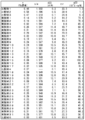
- FIG. 2 is a table showing the Yb concentration, lattice constant ratio c/a, and piezoelectric constant d 33 in each thin film.
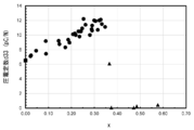
- 5 is a graph showing the relationship between the ytterbium concentration and the piezoelectric constant d 33 in the example of the first embodiment and the comparative example.
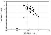
- 7 is a graph showing the relationship between the lattice constant ratio c/a and the piezoelectric constant d 33 in the example of the first embodiment and the comparative example.
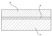
- FIG. 5 is a schematic side view of the piezoelectric thin film according to the second embodiment.
- FIG. 1 is a schematic side view of a piezoelectric thin film according to this embodiment. As shown in this figure, the piezoelectric thin film 1 is formed on a substrate 10.
- the thickness of the piezoelectric thin film is not particularly limited, but a range of 0.1 to 30 ⁇ m is preferable, and a range of 0.1 to 2 ⁇ m is particularly preferable because of excellent adhesion.
- the substrate 10 is not particularly limited in thickness, material and the like as long as the piezoelectric thin film 1 can be formed on the surface thereof.
- Examples of the substrate 10 include heat-resistant alloys such as silicon and Inconel, resin films such as polyimide, and the like.
- the piezoelectric thin film 1 is represented by the chemical formula Al 1-x Yb x N, the value of x is greater than 0 and less than 0.37, and the lattice constant ratio c/a is 1.53 or more and less than 1.6. It is composed of aluminum nitride added with ytterbium (Yb).
- the piezoelectric thin film having such a structure has a higher piezoelectric constant d 33 or g 33 than that of the aluminum nitride piezoelectric thin film to which ytterbium is not added.
- the value of x is in the range of more than 0.27 and less than 0.37.
- the piezoelectric thin film 1 having such a structure has a higher piezoelectric constant d 33 or g 33 .
- the value of x is in the range of more than 0.27 and less than 0.37 and the lattice constant ratio c/a is in the range of 1.53 or more and 1.555 or less. ..
- the piezoelectric thin film 1 having such a structure has a particularly high piezoelectric constant d 33 or g 33 .
- the value of x is in the range of more than 0 and less than 0.1.
- the piezoelectric thin film 1 having such a structure has a high piezoelectric constant d 33 or g 33 as compared with aluminum nitride to which ytterbium is not added, even if the amount of ytterbium added is small.
- the value of x is in the range of more than 0 and less than 0.1 and the lattice constant ratio c/a is 1.57 or more and less than 1.6.
- the piezoelectric thin film 1 having such a structure has a sufficiently high piezoelectric constant d 33 or g 33 even if the amount of ytterbium added is small.
- the sensor using the piezoelectric film 1 has low loss and can operate in a wide band. As a result, it is possible to make the portable device more compatible with high frequencies, downsized, and save power.
- the structure of the sensor is not particularly limited, and the sensor can be manufactured with a known structure.
- the piezoelectric thin film 1 can be manufactured by using a manufacturing method such as a sputtering method or a vapor deposition method, like a general piezoelectric thin film.
- a manufacturing method such as a sputtering method or a vapor deposition method, like a general piezoelectric thin film.
- the substrate 10 for example, a silicon (Si) substrate
- the substrate 10 can be manufactured by simultaneously subjecting a target composed of ytterbium and a target composed of aluminum to a sputtering process.
- a target made of an alloy containing ytterbium and aluminum in a predetermined ratio may be used.
- a plurality of aluminum nitride piezoelectric thin films to which ytterbium was added with a thickness of 0.4 to 1.5 ⁇ m were formed on an n-type silicon substrate having a specific resistance of 0.02 ⁇ cm using the following apparatus, a sputtering target, and the like.
- Sputtering device BC3263 (manufactured by ULVAC) Ytterbium sputtering target material (concentration: 99.999%)
- Aluminum sputtering target material (concentration: 99.999%)
- Substrate heating temperature 300-600°C
- the film forming experiment was performed after lowering the atmospheric pressure in the sputtering chamber with a vacuum pump so as to obtain a high vacuum of 10 ⁇ 6 or less. Further, in order to avoid mixing of impurities such as oxygen, the target surface was cleaned immediately after the target was mounted and immediately before each film forming experiment.
- FIG. 2 shows the concentration of ytterbium (Yb), the lattice constant ratio (c/a), d 33 , and the relative dielectric constants ⁇ r and g 33 of each of the obtained piezoelectric thin films.
- the lattice constant ratio c/a was calculated using an X-ray diffractometer (SmartLab, manufactured by Rigaku), and the piezoelectric constant d 33 and capacitance were measured using a piezometer (PM300, manufactured by Piezotest).
- the relative permittivity ⁇ r and g 33 were calculated from these values.
- the Yb concentration (x) was 5 for each sample by using an EDX apparatus (energy dispersive X-ray spectroscope, Horiba EX-420) in a scanning electron microscope (S-4300 manufactured by Hitachi High-Tech). It was measured at more than one place and the average value was adopted. At this time, the error of x was about ⁇ 0.003.
- EDX apparatus energy dispersive X-ray spectroscope, Horiba EX-420
- S-4300 manufactured by Hitachi High-Tech
- FIG. 3 A graph showing the relationship between the ytterbium concentration x and the piezoelectric constant d 33 is shown in FIG. 3, and a graph showing the relationship between the lattice constant ratio (c/a) and the piezoelectric constant d 33 is shown in FIG.
- a square mark indicates aluminum nitride to which ytterbium is not added
- a round mark indicates an example
- a triangle mark indicates a comparative example
- the piezoelectric constant d 33 of the piezoelectric thin film in which the value of x is in the range of more than 0 and less than 0.1 and the lattice constant ratio c/a is 1.57 or more and less than 1.6 is It was found that the piezoelectric constant d 33 was sufficiently high even if the amount of ytterbium used was small. (Embodiment 2)
- the piezoelectric thin film is directly formed on the substrate, but the present invention is not limited to this.
- the intermediate layer 20 may be provided between the substrate 10 and the piezoelectric thin film 1A.
- the intermediate layer 20 is not particularly limited in material, thickness and the like as long as the piezoelectric thin film 1A can be formed on the intermediate layer 20.
- the intermediate layer include aluminum nitride (AlN), gallium nitride (GaN), indium nitride (InN), titanium nitride (TiN), scandium nitride (ScN), ytterbium nitride (YbN), molybdenum (Mo), and tungsten (Mo).
- W hafnium (Hf), titanium (Ti), ruthenium (Ru), ruthenium oxide (RuO 2 ), chromium (Cr), chromium nitride, platinum (Pt), gold (Au), silver (Ag), copper ( Examples of the material include Cu), aluminum (Al), tantalum (Ta), iridium (Ir), palladium (Pd), nickel (Ni), and the like having a thickness of 50 to 200 nm.
- the crystallinity (crystallinity) of the piezoelectric thin film is improved, so that the piezoelectric film having a higher piezoelectricity than that of the aluminum nitride piezoelectric thin film to which ytterbium is not added is used.
- a ytterbium-doped aluminum nitride piezoelectric thin film having a constant d 33 or g 33 can be formed.
- the piezoelectric thin film is formed directly on the intermediate layer, but the present invention is not limited to this.
- a diffusion layer containing a substance forming the intermediate layer and a substance forming the piezoelectric thin film may be further provided between the intermediate layer and the piezoelectric thin film.
- the diffusion layer can be formed, for example, by forming a piezoelectric thin film on the intermediate layer and then applying heat thereto. Even if the diffusion layer is provided in this manner, the same effect as that of the second embodiment can be obtained.
Landscapes
- Engineering & Computer Science (AREA)
- Chemical & Material Sciences (AREA)
- Computer Hardware Design (AREA)
- Microelectronics & Electronic Packaging (AREA)
- Ceramic Engineering (AREA)
- Analytical Chemistry (AREA)
- Piezo-Electric Or Mechanical Vibrators, Or Delay Or Filter Circuits (AREA)
- Micromachines (AREA)
Priority Applications (4)
| Application Number | Priority Date | Filing Date | Title |
|---|---|---|---|
| CN201980076704.8A CN113165865B (zh) | 2018-12-11 | 2019-11-26 | 压电体以及使用其的mems器件 |
| KR1020217008026A KR102604213B1 (ko) | 2018-12-11 | 2019-11-26 | 압전체 및 이를 이용한 mems 디바이스 |
| EP19897007.1A EP3896029B1 (en) | 2018-12-11 | 2019-11-26 | Piezoelectric body and mems device using same |
| US17/276,464 US11968902B2 (en) | 2018-12-11 | 2019-11-26 | Piezoelectric body and MEMS device using same |
Applications Claiming Priority (2)
| Application Number | Priority Date | Filing Date | Title |
|---|---|---|---|
| JP2018231681A JP7085208B2 (ja) | 2018-12-11 | 2018-12-11 | 圧電体およびそれを用いたmemsデバイス |
| JP2018-231681 | 2018-12-11 |
Publications (1)
| Publication Number | Publication Date |
|---|---|
| WO2020121796A1 true WO2020121796A1 (ja) | 2020-06-18 |
Family
ID=71075954
Family Applications (1)
| Application Number | Title | Priority Date | Filing Date |
|---|---|---|---|
| PCT/JP2019/046052 Ceased WO2020121796A1 (ja) | 2018-12-11 | 2019-11-26 | 圧電体およびそれを用いたmemsデバイス |
Country Status (6)
| Country | Link |
|---|---|
| US (1) | US11968902B2 (enExample) |
| EP (1) | EP3896029B1 (enExample) |
| JP (1) | JP7085208B2 (enExample) |
| KR (1) | KR102604213B1 (enExample) |
| CN (1) | CN113165865B (enExample) |
| WO (1) | WO2020121796A1 (enExample) |
Families Citing this family (1)
| Publication number | Priority date | Publication date | Assignee | Title |
|---|---|---|---|---|
| JP7406262B2 (ja) * | 2019-02-22 | 2023-12-27 | 国立研究開発法人産業技術総合研究所 | 窒化物圧電体およびそれを用いたmemsデバイス |
Citations (5)
| Publication number | Priority date | Publication date | Assignee | Title |
|---|---|---|---|---|
| JP2002344279A (ja) * | 2001-05-11 | 2002-11-29 | Ube Electronics Ltd | 圧電薄膜共振子 |
| JP2005244184A (ja) * | 2004-01-28 | 2005-09-08 | Toshiba Corp | 薄膜圧電素子及び薄膜圧電素子の製造方法 |
| JP2009010926A (ja) | 2007-05-31 | 2009-01-15 | National Institute Of Advanced Industrial & Technology | 圧電体薄膜、圧電体およびそれらの製造方法、ならびに当該圧電体薄膜を用いた圧電体共振子、アクチュエータ素子および物理センサー |
| US20170263847A1 (en) | 2016-03-09 | 2017-09-14 | Teledyne Dalsa Semiconductor, Inc. | Piezoelectric Alloy Films |
| JP2017201050A (ja) | 2016-05-06 | 2017-11-09 | 学校法人早稲田大学 | 圧電体薄膜及びそれを用いた圧電素子 |
Family Cites Families (7)
| Publication number | Priority date | Publication date | Assignee | Title |
|---|---|---|---|---|
| US6936837B2 (en) | 2001-05-11 | 2005-08-30 | Ube Industries, Ltd. | Film bulk acoustic resonator |
| CN1983462B (zh) * | 2002-10-24 | 2010-11-03 | 精工爱普生株式会社 | 强电介质膜的制造方法、和强电介质电容器的制造方法 |
| JP4911907B2 (ja) * | 2005-03-25 | 2012-04-04 | 京セラ株式会社 | 圧電アクチュエータ及び液体吐出装置 |
| JP4977380B2 (ja) * | 2005-05-31 | 2012-07-18 | 京セラ株式会社 | 圧電アクチュエータおよびその駆動方法、並びに印刷ヘッド |
| TWI621183B (zh) * | 2011-12-01 | 2018-04-11 | 半導體能源研究所股份有限公司 | 半導體裝置及半導體裝置的製造方法 |
| US9520855B2 (en) * | 2014-02-26 | 2016-12-13 | Avago Technologies General Ip (Singapore) Pte. Ltd. | Bulk acoustic wave resonators having doped piezoelectric material and frame elements |
| JP7345855B2 (ja) * | 2020-02-27 | 2023-09-19 | 国立研究開発法人産業技術総合研究所 | 窒化物材料およびそれからなる圧電体並びにその圧電体を用いたmemsデバイス |
-
2018
- 2018-12-11 JP JP2018231681A patent/JP7085208B2/ja active Active
-
2019
- 2019-11-26 CN CN201980076704.8A patent/CN113165865B/zh active Active
- 2019-11-26 KR KR1020217008026A patent/KR102604213B1/ko active Active
- 2019-11-26 EP EP19897007.1A patent/EP3896029B1/en active Active
- 2019-11-26 WO PCT/JP2019/046052 patent/WO2020121796A1/ja not_active Ceased
- 2019-11-26 US US17/276,464 patent/US11968902B2/en active Active
Patent Citations (5)
| Publication number | Priority date | Publication date | Assignee | Title |
|---|---|---|---|---|
| JP2002344279A (ja) * | 2001-05-11 | 2002-11-29 | Ube Electronics Ltd | 圧電薄膜共振子 |
| JP2005244184A (ja) * | 2004-01-28 | 2005-09-08 | Toshiba Corp | 薄膜圧電素子及び薄膜圧電素子の製造方法 |
| JP2009010926A (ja) | 2007-05-31 | 2009-01-15 | National Institute Of Advanced Industrial & Technology | 圧電体薄膜、圧電体およびそれらの製造方法、ならびに当該圧電体薄膜を用いた圧電体共振子、アクチュエータ素子および物理センサー |
| US20170263847A1 (en) | 2016-03-09 | 2017-09-14 | Teledyne Dalsa Semiconductor, Inc. | Piezoelectric Alloy Films |
| JP2017201050A (ja) | 2016-05-06 | 2017-11-09 | 学校法人早稲田大学 | 圧電体薄膜及びそれを用いた圧電素子 |
Non-Patent Citations (1)
| Title |
|---|
| SHUJI TANAKA: "Sensor", vol. 22, 2012, JAPAN SOCIETY OF NEXT GENERATION SENSOR TECHNOLOGY, article "Revisiting the basics of vibration actuator with a view to a next generation sensor", pages: 14 - 17 |
Also Published As
| Publication number | Publication date |
|---|---|
| JP7085208B2 (ja) | 2022-06-16 |
| EP3896029A4 (en) | 2022-11-02 |
| JP2020096040A (ja) | 2020-06-18 |
| US11968902B2 (en) | 2024-04-23 |
| KR102604213B1 (ko) | 2023-11-20 |
| CN113165865B (zh) | 2024-05-14 |
| CN113165865A (zh) | 2021-07-23 |
| US20220037582A1 (en) | 2022-02-03 |
| EP3896029B1 (en) | 2023-08-23 |
| EP3896029A1 (en) | 2021-10-20 |
| EP3896029C0 (en) | 2023-08-23 |
| KR20210048513A (ko) | 2021-05-03 |
Similar Documents
| Publication | Publication Date | Title |
|---|---|---|
| JP5190841B2 (ja) | 圧電体薄膜、圧電体およびそれらの製造方法、ならびに当該圧電体薄膜を用いた圧電体共振子、アクチュエータ素子および物理センサー | |
| CN103415489B (zh) | 压电材料、压电元件、液体排出头、超声马达和去尘装置 | |
| US10637435B2 (en) | Bulk acoustic wave resonator and filter including the same | |
| CN107112977B (zh) | 压电膜以及压电振子 | |
| US9972769B2 (en) | Piezoelectric thin film and method for manufacturing the same, and piezoelectric element | |
| US10009007B2 (en) | Bulk acoustic wave resonator with a molybdenum tantalum alloy electrode and filter including the same | |
| CN110832654A (zh) | 压电薄膜元件 | |
| Fawzy et al. | Piezoelectric thin film materials for acoustic mems devices | |
| CN108574468A (zh) | 薄膜体声波谐振器以及制造薄膜体声波谐振器的方法 | |
| CN114341053B (zh) | 氮化物压电体和使用该氮化物压电体的mems器件 | |
| JP7085208B2 (ja) | 圧電体およびそれを用いたmemsデバイス | |
| KR102803105B1 (ko) | 질화물 재료 및 그것으로 이루어지는 압전체 및 그 압전체를 이용한 mems 디바이스, 트랜지스터, 인버터, 트랜스듀서, saw 디바이스 및 강유전체 메모리 | |
| TWI904882B (zh) | 氮化物材料及由其所成之壓電體以及使用該壓電體之mems裝置、與該氮化物材料及由其所成之強介電質以及使用該強介電質之電子元件 | |
| KR102380843B1 (ko) | 체적 음향 공진기 및 이를 포함하는 필터 | |
| CN113226982B (zh) | 氮化物压电体及使用其的mems器件 |
Legal Events
| Date | Code | Title | Description |
|---|---|---|---|
| 121 | Ep: the epo has been informed by wipo that ep was designated in this application |
Ref document number: 19897007 Country of ref document: EP Kind code of ref document: A1 |
|
| ENP | Entry into the national phase |
Ref document number: 20217008026 Country of ref document: KR Kind code of ref document: A |
|
| NENP | Non-entry into the national phase |
Ref country code: DE |
|
| ENP | Entry into the national phase |
Ref document number: 2019897007 Country of ref document: EP Effective date: 20210712 |