EP3896029B1 - Piezoelectric body and mems device using same - Google Patents
Piezoelectric body and mems device using same Download PDFInfo
- Publication number
- EP3896029B1 EP3896029B1 EP19897007.1A EP19897007A EP3896029B1 EP 3896029 B1 EP3896029 B1 EP 3896029B1 EP 19897007 A EP19897007 A EP 19897007A EP 3896029 B1 EP3896029 B1 EP 3896029B1
- Authority
- EP
- European Patent Office
- Prior art keywords
- piezoelectric
- piezoelectric body
- ytterbium
- less
- doped
- Prior art date
- Legal status (The legal status is an assumption and is not a legal conclusion. Google has not performed a legal analysis and makes no representation as to the accuracy of the status listed.)
- Active
Links
Images


Classifications
-
- H—ELECTRICITY
- H10—SEMICONDUCTOR DEVICES; ELECTRIC SOLID-STATE DEVICES NOT OTHERWISE PROVIDED FOR
- H10N—ELECTRIC SOLID-STATE DEVICES NOT OTHERWISE PROVIDED FOR
- H10N30/00—Piezoelectric or electrostrictive devices
- H10N30/30—Piezoelectric or electrostrictive devices with mechanical input and electrical output, e.g. functioning as generators or sensors
- H10N30/302—Sensors
-
- H—ELECTRICITY
- H10—SEMICONDUCTOR DEVICES; ELECTRIC SOLID-STATE DEVICES NOT OTHERWISE PROVIDED FOR
- H10N—ELECTRIC SOLID-STATE DEVICES NOT OTHERWISE PROVIDED FOR
- H10N30/00—Piezoelectric or electrostrictive devices
- H10N30/80—Constructional details
- H10N30/85—Piezoelectric or electrostrictive active materials
- H10N30/853—Ceramic compositions
-
- H—ELECTRICITY
- H10—SEMICONDUCTOR DEVICES; ELECTRIC SOLID-STATE DEVICES NOT OTHERWISE PROVIDED FOR
- H10N—ELECTRIC SOLID-STATE DEVICES NOT OTHERWISE PROVIDED FOR
- H10N30/00—Piezoelectric or electrostrictive devices
- H10N30/704—Piezoelectric or electrostrictive devices based on piezoelectric or electrostrictive films or coatings
- H10N30/706—Piezoelectric or electrostrictive devices based on piezoelectric or electrostrictive films or coatings characterised by the underlying bases, e.g. substrates
- H10N30/708—Intermediate layers, e.g. barrier, adhesion or growth control buffer layers
-
- B—PERFORMING OPERATIONS; TRANSPORTING
- B81—MICROSTRUCTURAL TECHNOLOGY
- B81B—MICROSTRUCTURAL DEVICES OR SYSTEMS, e.g. MICROMECHANICAL DEVICES
- B81B3/00—Devices comprising flexible or deformable elements, e.g. comprising elastic tongues or membranes
-
- B—PERFORMING OPERATIONS; TRANSPORTING
- B81—MICROSTRUCTURAL TECHNOLOGY
- B81B—MICROSTRUCTURAL DEVICES OR SYSTEMS, e.g. MICROMECHANICAL DEVICES
- B81B3/00—Devices comprising flexible or deformable elements, e.g. comprising elastic tongues or membranes
- B81B3/0018—Structures acting upon the moving or flexible element for transforming energy into mechanical movement or vice versa, i.e. actuators, sensors, generators
-
- H—ELECTRICITY
- H10—SEMICONDUCTOR DEVICES; ELECTRIC SOLID-STATE DEVICES NOT OTHERWISE PROVIDED FOR
- H10N—ELECTRIC SOLID-STATE DEVICES NOT OTHERWISE PROVIDED FOR
- H10N30/00—Piezoelectric or electrostrictive devices
- H10N30/20—Piezoelectric or electrostrictive devices with electrical input and mechanical output, e.g. functioning as actuators or vibrators
-
- H—ELECTRICITY
- H10—SEMICONDUCTOR DEVICES; ELECTRIC SOLID-STATE DEVICES NOT OTHERWISE PROVIDED FOR
- H10N—ELECTRIC SOLID-STATE DEVICES NOT OTHERWISE PROVIDED FOR
- H10N30/00—Piezoelectric or electrostrictive devices
- H10N30/30—Piezoelectric or electrostrictive devices with mechanical input and electrical output, e.g. functioning as generators or sensors
-
- H—ELECTRICITY
- H10—SEMICONDUCTOR DEVICES; ELECTRIC SOLID-STATE DEVICES NOT OTHERWISE PROVIDED FOR
- H10N—ELECTRIC SOLID-STATE DEVICES NOT OTHERWISE PROVIDED FOR
- H10N30/00—Piezoelectric or electrostrictive devices
- H10N30/50—Piezoelectric or electrostrictive devices having a stacked or multilayer structure
-
- B—PERFORMING OPERATIONS; TRANSPORTING
- B81—MICROSTRUCTURAL TECHNOLOGY
- B81B—MICROSTRUCTURAL DEVICES OR SYSTEMS, e.g. MICROMECHANICAL DEVICES
- B81B2201/00—Specific applications of microelectromechanical systems
- B81B2201/02—Sensors
- B81B2201/0228—Inertial sensors
- B81B2201/0235—Accelerometers
-
- B—PERFORMING OPERATIONS; TRANSPORTING
- B81—MICROSTRUCTURAL TECHNOLOGY
- B81B—MICROSTRUCTURAL DEVICES OR SYSTEMS, e.g. MICROMECHANICAL DEVICES
- B81B2201/00—Specific applications of microelectromechanical systems
- B81B2201/02—Sensors
- B81B2201/0228—Inertial sensors
- B81B2201/0242—Gyroscopes
-
- B—PERFORMING OPERATIONS; TRANSPORTING
- B81—MICROSTRUCTURAL TECHNOLOGY
- B81B—MICROSTRUCTURAL DEVICES OR SYSTEMS, e.g. MICROMECHANICAL DEVICES
- B81B2201/00—Specific applications of microelectromechanical systems
- B81B2201/02—Sensors
- B81B2201/0257—Microphones or microspeakers
-
- B—PERFORMING OPERATIONS; TRANSPORTING
- B81—MICROSTRUCTURAL TECHNOLOGY
- B81B—MICROSTRUCTURAL DEVICES OR SYSTEMS, e.g. MICROMECHANICAL DEVICES
- B81B2201/00—Specific applications of microelectromechanical systems
- B81B2201/02—Sensors
- B81B2201/0264—Pressure sensors
-
- H—ELECTRICITY
- H10—SEMICONDUCTOR DEVICES; ELECTRIC SOLID-STATE DEVICES NOT OTHERWISE PROVIDED FOR
- H10N—ELECTRIC SOLID-STATE DEVICES NOT OTHERWISE PROVIDED FOR
- H10N30/00—Piezoelectric or electrostrictive devices
- H10N30/01—Manufacture or treatment
- H10N30/07—Forming of piezoelectric or electrostrictive parts or bodies on an electrical element or another base
- H10N30/074—Forming of piezoelectric or electrostrictive parts or bodies on an electrical element or another base by depositing piezoelectric or electrostrictive layers, e.g. aerosol or screen printing
- H10N30/076—Forming of piezoelectric or electrostrictive parts or bodies on an electrical element or another base by depositing piezoelectric or electrostrictive layers, e.g. aerosol or screen printing by vapour phase deposition
Definitions
- the performance of the piezoelectric thin film is evaluated by using only the electromechanical coupling coefficient (k 2 ).
- the performance of the piezoelectric thin film should be evaluated against the performance index of each type of MEMS device.
- piezoelectric coefficients such as the level of strain caused by applying a voltage, i.e. d constant, and the voltage caused by applying a pressure, i.e. g constant, need to be evaluated.
- a voltage i.e. d constant
- a pressure i.e. g constant
- a third aspect according to the present invention is the piezoelectric body described in the second aspect, wherein the lattice constant ratio c/a is within a range of 1.53 or more and 1.555 or less.
- An eighth aspect of the present invention is the piezoelectric body described in the sixth or seventh aspect.
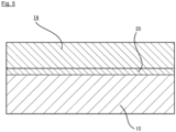
- a diffusion layer is further disposed between the intermediate layer and the piezoelectric body, and the diffusion layer includes a substance constituting the intermediate layer and a substance constituting the piezoelectric body.
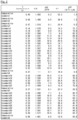
- FIG. 3 a graph showing the relation between the concentration x of ytterbium and the piezoelectric coefficient d 33 is shown in FIG. 3 and a graph showing the relation between the lattice constant ratio (c/a) and the piezoelectric coefficient d 33 is shown in FIG. 4 .
- the graph shows that the piezoelectric thin film in which the value of x was in a range of more than 0 and less than 0.1 and the lattice constant ratio c/a was in a range of 1.57 or more and less than 1.6 had the sufficiently high piezoelectric coefficient d 33 despite having been doped with less ytterbium.
Landscapes
- Engineering & Computer Science (AREA)
- Chemical & Material Sciences (AREA)
- Computer Hardware Design (AREA)
- Microelectronics & Electronic Packaging (AREA)
- Ceramic Engineering (AREA)
- Analytical Chemistry (AREA)
- Piezo-Electric Or Mechanical Vibrators, Or Delay Or Filter Circuits (AREA)
- Micromachines (AREA)
Applications Claiming Priority (2)
| Application Number | Priority Date | Filing Date | Title |
|---|---|---|---|
| JP2018231681A JP7085208B2 (ja) | 2018-12-11 | 2018-12-11 | 圧電体およびそれを用いたmemsデバイス |
| PCT/JP2019/046052 WO2020121796A1 (ja) | 2018-12-11 | 2019-11-26 | 圧電体およびそれを用いたmemsデバイス |
Publications (4)
| Publication Number | Publication Date |
|---|---|
| EP3896029A1 EP3896029A1 (en) | 2021-10-20 |
| EP3896029A4 EP3896029A4 (en) | 2022-11-02 |
| EP3896029B1 true EP3896029B1 (en) | 2023-08-23 |
| EP3896029C0 EP3896029C0 (en) | 2023-08-23 |
Family
ID=71075954
Family Applications (1)
| Application Number | Title | Priority Date | Filing Date |
|---|---|---|---|
| EP19897007.1A Active EP3896029B1 (en) | 2018-12-11 | 2019-11-26 | Piezoelectric body and mems device using same |
Country Status (6)
| Country | Link |
|---|---|
| US (1) | US11968902B2 (enExample) |
| EP (1) | EP3896029B1 (enExample) |
| JP (1) | JP7085208B2 (enExample) |
| KR (1) | KR102604213B1 (enExample) |
| CN (1) | CN113165865B (enExample) |
| WO (1) | WO2020121796A1 (enExample) |
Families Citing this family (1)
| Publication number | Priority date | Publication date | Assignee | Title |
|---|---|---|---|---|
| JP7406262B2 (ja) * | 2019-02-22 | 2023-12-27 | 国立研究開発法人産業技術総合研究所 | 窒化物圧電体およびそれを用いたmemsデバイス |
Family Cites Families (12)
| Publication number | Priority date | Publication date | Assignee | Title |
|---|---|---|---|---|
| JP4478910B2 (ja) * | 2001-05-11 | 2010-06-09 | 宇部興産株式会社 | 圧電薄膜共振子 |
| US6936837B2 (en) | 2001-05-11 | 2005-08-30 | Ube Industries, Ltd. | Film bulk acoustic resonator |
| CN1983462B (zh) * | 2002-10-24 | 2010-11-03 | 精工爱普生株式会社 | 强电介质膜的制造方法、和强电介质电容器的制造方法 |
| JP2005244184A (ja) * | 2004-01-28 | 2005-09-08 | Toshiba Corp | 薄膜圧電素子及び薄膜圧電素子の製造方法 |
| JP4911907B2 (ja) * | 2005-03-25 | 2012-04-04 | 京セラ株式会社 | 圧電アクチュエータ及び液体吐出装置 |
| JP4977380B2 (ja) * | 2005-05-31 | 2012-07-18 | 京セラ株式会社 | 圧電アクチュエータおよびその駆動方法、並びに印刷ヘッド |
| JP5190841B2 (ja) | 2007-05-31 | 2013-04-24 | 独立行政法人産業技術総合研究所 | 圧電体薄膜、圧電体およびそれらの製造方法、ならびに当該圧電体薄膜を用いた圧電体共振子、アクチュエータ素子および物理センサー |
| TWI621183B (zh) * | 2011-12-01 | 2018-04-11 | 半導體能源研究所股份有限公司 | 半導體裝置及半導體裝置的製造方法 |
| US9520855B2 (en) * | 2014-02-26 | 2016-12-13 | Avago Technologies General Ip (Singapore) Pte. Ltd. | Bulk acoustic wave resonators having doped piezoelectric material and frame elements |
| US20170263847A1 (en) * | 2016-03-09 | 2017-09-14 | Teledyne Dalsa Semiconductor, Inc. | Piezoelectric Alloy Films |
| JP2017201050A (ja) * | 2016-05-06 | 2017-11-09 | 学校法人早稲田大学 | 圧電体薄膜及びそれを用いた圧電素子 |
| JP7345855B2 (ja) * | 2020-02-27 | 2023-09-19 | 国立研究開発法人産業技術総合研究所 | 窒化物材料およびそれからなる圧電体並びにその圧電体を用いたmemsデバイス |
-
2018
- 2018-12-11 JP JP2018231681A patent/JP7085208B2/ja active Active
-
2019
- 2019-11-26 CN CN201980076704.8A patent/CN113165865B/zh active Active
- 2019-11-26 KR KR1020217008026A patent/KR102604213B1/ko active Active
- 2019-11-26 EP EP19897007.1A patent/EP3896029B1/en active Active
- 2019-11-26 WO PCT/JP2019/046052 patent/WO2020121796A1/ja not_active Ceased
- 2019-11-26 US US17/276,464 patent/US11968902B2/en active Active
Also Published As
| Publication number | Publication date |
|---|---|
| JP7085208B2 (ja) | 2022-06-16 |
| EP3896029A4 (en) | 2022-11-02 |
| JP2020096040A (ja) | 2020-06-18 |
| US11968902B2 (en) | 2024-04-23 |
| KR102604213B1 (ko) | 2023-11-20 |
| CN113165865B (zh) | 2024-05-14 |
| CN113165865A (zh) | 2021-07-23 |
| WO2020121796A1 (ja) | 2020-06-18 |
| US20220037582A1 (en) | 2022-02-03 |
| EP3896029A1 (en) | 2021-10-20 |
| EP3896029C0 (en) | 2023-08-23 |
| KR20210048513A (ko) | 2021-05-03 |
Similar Documents
| Publication | Publication Date | Title |
|---|---|---|
| Mertin et al. | Piezoelectric and structural properties of c-axis textured aluminium scandium nitride thin films up to high scandium content | |
| CN101325240B (zh) | 压电体薄膜、压电体及其制造方法、以及压电体谐振子 | |
| US10637435B2 (en) | Bulk acoustic wave resonator and filter including the same | |
| US7758979B2 (en) | Piezoelectric thin film, piezoelectric material, and fabrication method of piezoelectric thin film and piezoelectric material, and piezoelectric resonator, actuator element, and physical sensor using piezoelectric thin film | |
| CN101322258B (zh) | 压电元件及其制造方法 | |
| Mertin et al. | Enhanced piezoelectric properties of c-axis textured aluminium scandium nitride thin films with high scandium content: Influence of intrinsic stress and sputtering parameters | |
| Lin et al. | Highly sensitive mass sensor using film bulk acoustic resonator | |
| US10009007B2 (en) | Bulk acoustic wave resonator with a molybdenum tantalum alloy electrode and filter including the same | |
| EP3216894A1 (en) | Piezoelectric alloy films | |
| CN107112977A (zh) | 压电膜以及压电振子 | |
| US11558031B2 (en) | Film bulk acoustic resonator and method of manufacturing the same | |
| Fawzy et al. | Piezoelectric thin film materials for acoustic mems devices | |
| US11968902B2 (en) | Piezoelectric body and MEMS device using same | |
| CN114341053B (zh) | 氮化物压电体和使用该氮化物压电体的mems器件 | |
| WO2004066406A2 (ja) | 圧電素子およびその製造方法 | |
| TWI904882B (zh) | 氮化物材料及由其所成之壓電體以及使用該壓電體之mems裝置、與該氮化物材料及由其所成之強介電質以及使用該強介電質之電子元件 | |
| Chandra et al. | Preparation and characterization of piezoelectric films of ZnO and AlN by RF sputtering for RF MEMS applications | |
| Lin et al. | Growth of highly c-axis oriented AlN films on 3C–SiC/Si substrate | |
| Ralib et al. | Dependence of preferred c-axis orientation on RF magnetron sputtering power for AZO/Si acoustic wave devices |
Legal Events
| Date | Code | Title | Description |
|---|---|---|---|
| STAA | Information on the status of an ep patent application or granted ep patent |
Free format text: STATUS: THE INTERNATIONAL PUBLICATION HAS BEEN MADE |
|
| PUAI | Public reference made under article 153(3) epc to a published international application that has entered the european phase |
Free format text: ORIGINAL CODE: 0009012 |
|
| STAA | Information on the status of an ep patent application or granted ep patent |
Free format text: STATUS: REQUEST FOR EXAMINATION WAS MADE |
|
| 17P | Request for examination filed |
Effective date: 20210414 |
|
| AK | Designated contracting states |
Kind code of ref document: A1 Designated state(s): AL AT BE BG CH CY CZ DE DK EE ES FI FR GB GR HR HU IE IS IT LI LT LU LV MC MK MT NL NO PL PT RO RS SE SI SK SM TR |
|
| DAV | Request for validation of the european patent (deleted) | ||
| DAX | Request for extension of the european patent (deleted) | ||
| A4 | Supplementary search report drawn up and despatched |
Effective date: 20220929 |
|
| RIC1 | Information provided on ipc code assigned before grant |
Ipc: H01L 41/08 20060101ALI20220923BHEP Ipc: H01L 41/187 20060101AFI20220923BHEP |
|
| REG | Reference to a national code |
Ref country code: DE Ref legal event code: R079 Free format text: PREVIOUS MAIN CLASS: B81B0003000000 Ipc: H10N0030000000 Ref document number: 602019035857 Country of ref document: DE |
|
| GRAP | Despatch of communication of intention to grant a patent |
Free format text: ORIGINAL CODE: EPIDOSNIGR1 |
|
| STAA | Information on the status of an ep patent application or granted ep patent |
Free format text: STATUS: GRANT OF PATENT IS INTENDED |
|
| RIC1 | Information provided on ipc code assigned before grant |
Ipc: H10N 30/853 20230101ALI20230224BHEP Ipc: H10N 30/00 20230101AFI20230224BHEP |
|
| INTG | Intention to grant announced |
Effective date: 20230329 |
|
| RIN1 | Information on inventor provided before grant (corrected) |
Inventor name: HIRATA KENJI Inventor name: ANGGRAINI SRI AYU Inventor name: AKIYAMA MORITO Inventor name: YAMADA HIROSHI Inventor name: UEHARA MASATO |
|
| GRAS | Grant fee paid |
Free format text: ORIGINAL CODE: EPIDOSNIGR3 |
|
| GRAA | (expected) grant |
Free format text: ORIGINAL CODE: 0009210 |
|
| STAA | Information on the status of an ep patent application or granted ep patent |
Free format text: STATUS: THE PATENT HAS BEEN GRANTED |
|
| AK | Designated contracting states |
Kind code of ref document: B1 Designated state(s): AL AT BE BG CH CY CZ DE DK EE ES FI FR GB GR HR HU IE IS IT LI LT LU LV MC MK MT NL NO PL PT RO RS SE SI SK SM TR |
|
| REG | Reference to a national code |
Ref country code: GB Ref legal event code: FG4D |
|
| REG | Reference to a national code |
Ref country code: CH Ref legal event code: EP |
|
| REG | Reference to a national code |
Ref country code: IE Ref legal event code: FG4D |
|
| REG | Reference to a national code |
Ref country code: DE Ref legal event code: R096 Ref document number: 602019035857 Country of ref document: DE |
|
| U01 | Request for unitary effect filed |
Effective date: 20230823 |
|
| U07 | Unitary effect registered |
Designated state(s): AT BE BG DE DK EE FI FR IT LT LU LV MT NL PT SE SI Effective date: 20230828 |
|
| U20 | Renewal fee for the european patent with unitary effect paid |
Year of fee payment: 5 Effective date: 20230919 |
|
| PG25 | Lapsed in a contracting state [announced via postgrant information from national office to epo] |
Ref country code: GR Free format text: LAPSE BECAUSE OF FAILURE TO SUBMIT A TRANSLATION OF THE DESCRIPTION OR TO PAY THE FEE WITHIN THE PRESCRIBED TIME-LIMIT Effective date: 20231124 |
|
| PG25 | Lapsed in a contracting state [announced via postgrant information from national office to epo] |
Ref country code: IS Free format text: LAPSE BECAUSE OF FAILURE TO SUBMIT A TRANSLATION OF THE DESCRIPTION OR TO PAY THE FEE WITHIN THE PRESCRIBED TIME-LIMIT Effective date: 20231223 |
|
| PG25 | Lapsed in a contracting state [announced via postgrant information from national office to epo] |
Ref country code: RS Free format text: LAPSE BECAUSE OF FAILURE TO SUBMIT A TRANSLATION OF THE DESCRIPTION OR TO PAY THE FEE WITHIN THE PRESCRIBED TIME-LIMIT Effective date: 20230823 Ref country code: NO Free format text: LAPSE BECAUSE OF FAILURE TO SUBMIT A TRANSLATION OF THE DESCRIPTION OR TO PAY THE FEE WITHIN THE PRESCRIBED TIME-LIMIT Effective date: 20231123 Ref country code: IS Free format text: LAPSE BECAUSE OF FAILURE TO SUBMIT A TRANSLATION OF THE DESCRIPTION OR TO PAY THE FEE WITHIN THE PRESCRIBED TIME-LIMIT Effective date: 20231223 Ref country code: HR Free format text: LAPSE BECAUSE OF FAILURE TO SUBMIT A TRANSLATION OF THE DESCRIPTION OR TO PAY THE FEE WITHIN THE PRESCRIBED TIME-LIMIT Effective date: 20230823 Ref country code: GR Free format text: LAPSE BECAUSE OF FAILURE TO SUBMIT A TRANSLATION OF THE DESCRIPTION OR TO PAY THE FEE WITHIN THE PRESCRIBED TIME-LIMIT Effective date: 20231124 |
|
| PG25 | Lapsed in a contracting state [announced via postgrant information from national office to epo] |
Ref country code: PL Free format text: LAPSE BECAUSE OF FAILURE TO SUBMIT A TRANSLATION OF THE DESCRIPTION OR TO PAY THE FEE WITHIN THE PRESCRIBED TIME-LIMIT Effective date: 20230823 |
|
| PG25 | Lapsed in a contracting state [announced via postgrant information from national office to epo] |
Ref country code: ES Free format text: LAPSE BECAUSE OF FAILURE TO SUBMIT A TRANSLATION OF THE DESCRIPTION OR TO PAY THE FEE WITHIN THE PRESCRIBED TIME-LIMIT Effective date: 20230823 |
|
| PG25 | Lapsed in a contracting state [announced via postgrant information from national office to epo] |
Ref country code: SM Free format text: LAPSE BECAUSE OF FAILURE TO SUBMIT A TRANSLATION OF THE DESCRIPTION OR TO PAY THE FEE WITHIN THE PRESCRIBED TIME-LIMIT Effective date: 20230823 Ref country code: RO Free format text: LAPSE BECAUSE OF FAILURE TO SUBMIT A TRANSLATION OF THE DESCRIPTION OR TO PAY THE FEE WITHIN THE PRESCRIBED TIME-LIMIT Effective date: 20230823 Ref country code: ES Free format text: LAPSE BECAUSE OF FAILURE TO SUBMIT A TRANSLATION OF THE DESCRIPTION OR TO PAY THE FEE WITHIN THE PRESCRIBED TIME-LIMIT Effective date: 20230823 Ref country code: CZ Free format text: LAPSE BECAUSE OF FAILURE TO SUBMIT A TRANSLATION OF THE DESCRIPTION OR TO PAY THE FEE WITHIN THE PRESCRIBED TIME-LIMIT Effective date: 20230823 Ref country code: SK Free format text: LAPSE BECAUSE OF FAILURE TO SUBMIT A TRANSLATION OF THE DESCRIPTION OR TO PAY THE FEE WITHIN THE PRESCRIBED TIME-LIMIT Effective date: 20230823 |
|
| REG | Reference to a national code |
Ref country code: DE Ref legal event code: R097 Ref document number: 602019035857 Country of ref document: DE |
|
| PLBE | No opposition filed within time limit |
Free format text: ORIGINAL CODE: 0009261 |
|
| STAA | Information on the status of an ep patent application or granted ep patent |
Free format text: STATUS: NO OPPOSITION FILED WITHIN TIME LIMIT |
|
| PG25 | Lapsed in a contracting state [announced via postgrant information from national office to epo] |
Ref country code: MC Free format text: LAPSE BECAUSE OF FAILURE TO SUBMIT A TRANSLATION OF THE DESCRIPTION OR TO PAY THE FEE WITHIN THE PRESCRIBED TIME-LIMIT Effective date: 20230823 |
|
| GBPC | Gb: european patent ceased through non-payment of renewal fee |
Effective date: 20231126 |
|
| 26N | No opposition filed |
Effective date: 20240524 |
|
| PG25 | Lapsed in a contracting state [announced via postgrant information from national office to epo] |
Ref country code: MC Free format text: LAPSE BECAUSE OF FAILURE TO SUBMIT A TRANSLATION OF THE DESCRIPTION OR TO PAY THE FEE WITHIN THE PRESCRIBED TIME-LIMIT Effective date: 20230823 |
|
| REG | Reference to a national code |
Ref country code: IE Ref legal event code: MM4A |
|
| PG25 | Lapsed in a contracting state [announced via postgrant information from national office to epo] |
Ref country code: IE Free format text: LAPSE BECAUSE OF NON-PAYMENT OF DUE FEES Effective date: 20231126 |
|
| PG25 | Lapsed in a contracting state [announced via postgrant information from national office to epo] |
Ref country code: GB Free format text: LAPSE BECAUSE OF NON-PAYMENT OF DUE FEES Effective date: 20231126 |
|
| PG25 | Lapsed in a contracting state [announced via postgrant information from national office to epo] |
Ref country code: IE Free format text: LAPSE BECAUSE OF NON-PAYMENT OF DUE FEES Effective date: 20231126 Ref country code: GB Free format text: LAPSE BECAUSE OF NON-PAYMENT OF DUE FEES Effective date: 20231126 |
|
| U20 | Renewal fee for the european patent with unitary effect paid |
Year of fee payment: 6 Effective date: 20241122 |
|
| PG25 | Lapsed in a contracting state [announced via postgrant information from national office to epo] |
Ref country code: CY Free format text: LAPSE BECAUSE OF FAILURE TO SUBMIT A TRANSLATION OF THE DESCRIPTION OR TO PAY THE FEE WITHIN THE PRESCRIBED TIME-LIMIT; INVALID AB INITIO Effective date: 20191126 |
|
| PG25 | Lapsed in a contracting state [announced via postgrant information from national office to epo] |
Ref country code: HU Free format text: LAPSE BECAUSE OF FAILURE TO SUBMIT A TRANSLATION OF THE DESCRIPTION OR TO PAY THE FEE WITHIN THE PRESCRIBED TIME-LIMIT; INVALID AB INITIO Effective date: 20191126 |
|
| REG | Reference to a national code |
Ref country code: CH Ref legal event code: U11 Free format text: ST27 STATUS EVENT CODE: U-0-0-U10-U11 (AS PROVIDED BY THE NATIONAL OFFICE) Effective date: 20251201 |
|
| PG25 | Lapsed in a contracting state [announced via postgrant information from national office to epo] |
Ref country code: TR Free format text: LAPSE BECAUSE OF FAILURE TO SUBMIT A TRANSLATION OF THE DESCRIPTION OR TO PAY THE FEE WITHIN THE PRESCRIBED TIME-LIMIT Effective date: 20230823 |
|
| U20 | Renewal fee for the european patent with unitary effect paid |
Year of fee payment: 7 Effective date: 20251124 |
|
| PGFP | Annual fee paid to national office [announced via postgrant information from national office to epo] |
Ref country code: CH Payment date: 20251201 Year of fee payment: 7 |