WO2020121581A1 - プラズマ処理装置 - Google Patents
プラズマ処理装置 Download PDFInfo
- Publication number
- WO2020121581A1 WO2020121581A1 PCT/JP2019/028262 JP2019028262W WO2020121581A1 WO 2020121581 A1 WO2020121581 A1 WO 2020121581A1 JP 2019028262 W JP2019028262 W JP 2019028262W WO 2020121581 A1 WO2020121581 A1 WO 2020121581A1
- Authority
- WO
- WIPO (PCT)
- Prior art keywords
- gas
- gas supply
- shower plate
- plasma processing
- processing apparatus
- Prior art date
- Legal status (The legal status is an assumption and is not a legal conclusion. Google has not performed a legal analysis and makes no representation as to the accuracy of the status listed.)
- Ceased
Links
Images








Classifications
-
- H—ELECTRICITY
- H01—ELECTRIC ELEMENTS
- H01J—ELECTRIC DISCHARGE TUBES OR DISCHARGE LAMPS
- H01J37/00—Discharge tubes with provision for introducing objects or material to be exposed to the discharge, e.g. for the purpose of examination or processing thereof
- H01J37/32—Gas-filled discharge tubes
- H01J37/32431—Constructional details of the reactor
- H01J37/3244—Gas supply means
-
- H—ELECTRICITY
- H01—ELECTRIC ELEMENTS
- H01J—ELECTRIC DISCHARGE TUBES OR DISCHARGE LAMPS
- H01J37/00—Discharge tubes with provision for introducing objects or material to be exposed to the discharge, e.g. for the purpose of examination or processing thereof
- H01J37/32—Gas-filled discharge tubes
- H01J37/32431—Constructional details of the reactor
- H01J37/3244—Gas supply means
- H01J37/32449—Gas control, e.g. control of the gas flow
-
- H—ELECTRICITY
- H01—ELECTRIC ELEMENTS
- H01J—ELECTRIC DISCHARGE TUBES OR DISCHARGE LAMPS
- H01J37/00—Discharge tubes with provision for introducing objects or material to be exposed to the discharge, e.g. for the purpose of examination or processing thereof
- H01J37/32—Gas-filled discharge tubes
- H01J37/32009—Arrangements for generation of plasma specially adapted for examination or treatment of objects, e.g. plasma sources
- H01J37/32082—Radio frequency generated discharge
-
- H—ELECTRICITY
- H01—ELECTRIC ELEMENTS
- H01J—ELECTRIC DISCHARGE TUBES OR DISCHARGE LAMPS
- H01J37/00—Discharge tubes with provision for introducing objects or material to be exposed to the discharge, e.g. for the purpose of examination or processing thereof
- H01J37/32—Gas-filled discharge tubes
- H01J37/32009—Arrangements for generation of plasma specially adapted for examination or treatment of objects, e.g. plasma sources
- H01J37/32082—Radio frequency generated discharge
- H01J37/32174—Circuits specially adapted for controlling the RF discharge
-
- H—ELECTRICITY
- H01—ELECTRIC ELEMENTS
- H01J—ELECTRIC DISCHARGE TUBES OR DISCHARGE LAMPS
- H01J37/00—Discharge tubes with provision for introducing objects or material to be exposed to the discharge, e.g. for the purpose of examination or processing thereof
- H01J37/32—Gas-filled discharge tubes
- H01J37/32431—Constructional details of the reactor
- H01J37/3266—Magnetic control means
- H01J37/32678—Electron cyclotron resonance
-
- H—ELECTRICITY
- H10—SEMICONDUCTOR DEVICES; ELECTRIC SOLID-STATE DEVICES NOT OTHERWISE PROVIDED FOR
- H10P—GENERIC PROCESSES OR APPARATUS FOR THE MANUFACTURE OR TREATMENT OF DEVICES COVERED BY CLASS H10
- H10P50/00—Etching of wafers, substrates or parts of devices
- H10P50/20—Dry etching; Plasma etching; Reactive-ion etching
- H10P50/24—Dry etching; Plasma etching; Reactive-ion etching of semiconductor materials
- H10P50/242—Dry etching; Plasma etching; Reactive-ion etching of semiconductor materials of Group IV materials
-
- H—ELECTRICITY
- H01—ELECTRIC ELEMENTS
- H01J—ELECTRIC DISCHARGE TUBES OR DISCHARGE LAMPS
- H01J2237/00—Discharge tubes exposing object to beam, e.g. for analysis treatment, etching, imaging
- H01J2237/32—Processing objects by plasma generation
- H01J2237/33—Processing objects by plasma generation characterised by the type of processing
- H01J2237/334—Etching
- H01J2237/3343—Problems associated with etching
Definitions
- the present invention relates to a plasma processing device.
- lithography technology is used to form fine patterns in the manufacturing process of semiconductor devices. This technique applies a device structure pattern on a resist layer and selectively etches away the substrate exposed by the resist layer pattern. In subsequent processing steps, other materials may be deposited in the etched areas to form integrated circuits.
- ECR Electro Cyclotron Resonance
- inductive coupling Inductive coupling
- capacitive coupling As a plasma generation method in the plasma etching apparatus, methods such as ECR (Electron Cyclotron Resonance), inductive coupling, and capacitive coupling are known.
- the ECR method is a plasma generation method that utilizes a resonance phenomenon in which the rotation frequency of electrons rotating around magnetic lines of force matches the microwave frequency.
- the ECR plasma generation method is characterized in that the generation region of ECR plasma can be changed by controlling the coil magnetic field to control the ion flux distribution in the wafer surface.
- an ECR-type plasma etching apparatus that uses microwaves, in order to ensure the uniformity of ion flux distribution on the wafer, by controlling the current value of the electromagnetic coil, an equal magnetic field surface (ECR surface) of 875G, which is the plasma generation region, is controlled. ) Position control and ion transport control by adjusting the direction of magnetic field lines are often used.
- Patent Document 1 discloses a configuration in which a ceramic shower plate for supplying gas into the inductively coupled plasma processing apparatus and a gas injector in the central portion are arranged.
- the flow velocity distribution in the device can be adjusted by adjusting the gas flow rates supplied to the central gas injector and the ceramic shower plate, respectively.
- the gas is supplied from the central gas injector, a high flow velocity can be realized on the central axis of the device, and if the gas is supplied from the ceramic shower plate, a uniform gas flow can be realized in the device.
- the transport of the reaction products generated from the wafer is adjusted by the gas flow, which contributes to uniformization of the density distribution of the reaction products on the wafer.
- microwaves are input on the central axis of the apparatus in order to obtain an axially symmetric microwave electric field, so that a structure such as a gas injector or a pipe toward the gas injector is installed in the central part of the apparatus.
- a structure such as a gas injector or a pipe toward the gas injector is installed in the central part of the apparatus.
- the axial symmetry of the microwave electric field distribution is disturbed.
- the plasma density distribution is biased and the processing uniformity is deteriorated.
- use a shower plate in which gas hole arrangement is optimized so as to obtain a desired reaction product density distribution Is one idea.
- the gas is supplied centrally to the central axis of the apparatus, so that the gas flow velocity in the central part of the wafer can be increased.
- a shower plate having gas holes arranged on the entire surface is used, a relatively uniform gas flow can be formed in the apparatus.
- plasma processing must be performed while replacing the shower plate with the optimal hole arrangement for each processing condition. If the plasma processing apparatus is stopped each time, the production efficiency will be significantly reduced.
- a technique of supplying different gases from the vicinity of the central axis of the device and the outer periphery is well known.
- the gas density a radial distribution in the vicinity of the ECR plane, which is a radical generation region.
- the direction of gas injection from the outer periphery is oriented so as not to face the center of the apparatus so that radicals generated by the gas supplied from the outer periphery are supplied to the outer periphery of the wafer.
- Patent Document 2 discloses a configuration in which gas from the outer periphery is supplied obliquely downward from a ring-shaped member at the outer peripheral portion of the apparatus
- Patent Document 3 discloses a configuration in which a space between a shower plate and a dielectric window is provided.
- radicals and reaction products excessively deposited on the inner wall of the apparatus may be peeled off and adhere to the wafer as foreign matter.
- the yield at the time of manufacturing semiconductor devices decreases. Therefore, after the wafer processing, it is necessary to generate plasma using a cleaning gas such as SF 6 /O 2 and clean the inner wall of the device with ions or radicals.
- the conductance of the gas changes over time due to the accumulation of radicals and reaction products in the gaps through which the gas passes. That is, when a large number of wafers are continuously processed under the same processing conditions, the processing results change over time, which makes it difficult to mass-produce semiconductor devices of the same level.
- the gap between the gas introduction ring and the ring cover is narrowed, the flow velocity of the gas ejected from the gap becomes faster, and the radicals and reaction products generated in the processing chamber are less likely to be transported into the gap, It becomes easy to suppress the attachment of radicals and reaction products in the gap.
- the gap is narrow, the influence of the tolerance of the ring-shaped member and the human error of the mounting position becomes relatively large with respect to the size of the gap. If the gaps in the circumferential direction become non-uniform, the amount of gas jetted to the device becomes non-uniform in the circumferential direction, which hinders uniformization of the desired radical density distribution.
- the gas from the outer periphery is supplied with some initial velocity in the direction toward the center axis of the device. Therefore, the gas supplied from the outer periphery is mixed with the gas supplied from the shower plate and transported to the wafer. Therefore, in order to supply a large amount of desired radicals to the outer peripheral portion of the wafer, even if a desired gas is supplied from the outer peripheral portion, the radicals are likely to be transported to the central portion of the wafer due to the gas flow, and it is difficult to perform the desired supply.
- the shower plate will bend due to the pressure difference between the front and back of the shower plate.
- the adhesion between the partition portion of the dielectric window and the shower plate is impaired, and there is a risk that the central side and outer peripheral side flow paths will be connected between the dielectric window and the shower plate.
- the gas is supplied from the shower plate to the processing chamber in a mixed state, making it difficult to supply independent gas.
- the present invention has been made in view of the above problems, and provides a plasma processing apparatus capable of adjusting the density distribution of radicals and reaction products on a wafer by using two shower plates provided with gas holes.
- the purpose is to do.
- one of the typical plasma processing apparatuses is a processing chamber in which a sample is plasma-processed, a high-frequency power supply that supplies high-frequency power for generating plasma, and the processing.
- a dielectric plate disposed above the chamber to hermetically seal the processing chamber, a first gas supply plate disposed below the dielectric plate to supply a first gas into the processing chamber, and the sample And a sample table on which is mounted, further comprising a second gas supply plate disposed below the first gas supply plate for supplying a second gas into the processing chamber,
- the first gas supply plate has a plurality of first gas holes penetrating the first region, and the second gas supply plate has second gas holes in the second region.
- a plurality of through holes are formed, and the space between the dielectric plate and the first gas supply plate is supplied with the first gas by the first gas supply means.
- the second gas is supplied to the space between the second gas supply plate and the second gas supply plate, and the first region is a central region of the first gas supply plate.
- the second region is achieved by including the first region and wider than the first region.
- FIG. 1 is a sectional view of a plasma etching apparatus according to the first embodiment of the present invention.
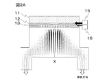
- FIG. 2A is a flow velocity pattern diagram in the plasma etching apparatus according to the first embodiment of the present invention.
- FIG. 2B is a flow rate pattern diagram in the plasma etching apparatus according to the first embodiment of the present invention.
- FIG. 3 is a sectional view of a plasma etching apparatus according to the second embodiment of the present invention.
- FIG. 4 is an enlarged sectional view of a dielectric window and a shower plate according to the second embodiment of the present invention.
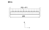
- FIG. 5A is a diagram showing a structural model of a shower plate according to the second embodiment of the present invention.
- FIG. 5B is a diagram showing a structural model of the shower plate according to the second embodiment of the present invention.
- FIG. 6 is an equivalent circuit diagram of a gas flow according to the second embodiment of the present invention.
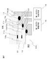
- FIG. 7 is an enlarged cross-sectional view of the outer periphery of the dielectric window and the shower plate according to the third embodiment of the present invention.
- FIG. 8A is a bottom view of a dielectric window according to the third embodiment of the present invention.
- FIG. 8B is a bottom view of the upper shower plate according to the third embodiment of the present invention.
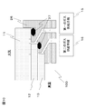
- FIG. 9 is an enlarged cross-sectional view of the dielectric window and the outer peripheral portion of the shower plate representing another embodiment.
- FIG. 10 is an enlarged cross-sectional view of a dielectric window and a shower plate outer peripheral portion representing another embodiment.
- FIG. 11 is an enlarged cross-sectional view of a dielectric window and a shower plate outer peripheral portion representing another embodiment.
- upper means a side farther from the substrate to be processed along a normal line extending from the surface to be processed of the substrate to be processed without passing through the inside of the substrate
- lower means The side closer to the substrate to be processed along the normal line is referred to.
- the central axis of the apparatus passes through the center of the substrate to be processed.
- FIG. 1 shows a cross-sectional view of a plasma etching apparatus according to the first embodiment of the present invention.
- the microwave oscillated from the microwave source 1 is transmitted to the circular waveguide 6 via the rectangular waveguide 2, the automatic matching machine 3, the isolator 4, and the circular-rectangular converter 5.
- the microwave source 1 is a 2.45 GHz magnetron that is often used as an industrial frequency.
- the frequency is not limited to this, and electromagnetic waves of several tens of MHz to several tens of GHz may be used.
- Automatic matching machine 3 has a role of adjusting load impedance, suppressing reflected waves, and efficiently supplying electromagnetic waves. Further, an isolator 4 is used to protect the microwave source 1 from reflected waves.
- the circular waveguide 6 is preferably selected to have a diameter that propagates only the circular TE11 mode, which is the fundamental mode. As a result, when a higher-order mode is included, it is possible to suppress adverse effects on the stability and uniformity of plasma generation.
- the circular waveguide 6 is connected to the cavity 7, and the cavity 7 has a function of adjusting the electromagnetic field distribution to a distribution suitable for plasma processing.
- An electromagnetic coil 8 is provided around a plasma processing chamber (also simply referred to as a processing chamber) 100, and a yoke 9 is provided on the outer periphery thereof.
- a plasma processing chamber also simply referred to as a processing chamber
- a yoke 9 is provided on the outer periphery thereof.
- the magnetic lines of force formed by the electromagnetic coil 8 and the yoke 9 become a diffusion magnetic field that spreads from the upper side to the lower side in the plasma processing chamber 100 in the outer peripheral direction.
- the magnetic flux density required for ECR is 875 G.
- a circular plate-shaped microwave introduction window (also referred to as a dielectric plate) 11 that hermetically seals the plasma processing chamber 100, an upper shower plate (first gas supply plate) 12, and a lower shower are provided under the cavity 7.
- the plate (second gas supply plate) 13 and the inner cylinder 14 are arranged in this order from above.
- quartz that efficiently transmits microwaves and has excellent plasma resistance.
- yttria, alumina, yttrium fluoride, aluminum fluoride, aluminum nitride, or the like which has high plasma resistance and transmits microwaves may be used.
- the inner cylinder 14 does not necessarily need to transmit microwaves, but it must have plasma resistance from the viewpoint of suppressing foreign matter and contamination of the wafer due to sputtering of the inner cylinder 14. Therefore, for example, quartz is preferably used as the material of the inner cylinder 14, but yttria, alumina, yttrium fluoride, aluminum fluoride, aluminum nitride or the like may be used.
- the inner cylinder 14 and the chamber inner wall 25 (described later) constitute a vacuum container.
- the first gas is supplied from the first gas supply means 15 to the space between the microwave introduction window 11 and the upper shower plate 12.
- a second gas is supplied from the second gas supply means 16 to the space between the upper shower plate 12 and the lower shower plate 13.
- the first gas supply means 15 and the second gas supply means 16 include a function of independently supplying a desired flow rate by, for example, a mass flow controller (control device). Further, the first gas supply means 15 and the second gas supply means 16 include a function of supplying a plurality of gas species in combination at a predetermined flow rate.
- the upper shower plate 12 has a plurality of gas holes (first gas holes) 12p
- the lower shower plate 13 has a plurality of gas holes (second gas holes) 13p.
- the processing gas is supplied to the plasma processing chamber 100 through the gas holes 12p and 13p.
- a substrate stage/high frequency electrode (sample stage) 17 which is arranged so as to face the lower shower plate 13 and on which the substrate 10 to be processed is mounted, and an insulating plate 18 which is arranged below the substrate stage.
- the gas supplied from the first gas supply means 15 and the second gas supply means 16 into the plasma processing chamber 100 is discharged from the lower part of the plasma processing chamber 100 to the outside by the turbo molecular pump 20 via the conductance adjusting valve 19. It is configured to be evacuated.
- a bias power source 22 is connected to the substrate stage/high frequency electrode 17 via an automatic matching machine for bias 21.
- the bias power source having a frequency of 400 kHz is used, but other frequencies such as an industrial frequency of 13.56 MHz may be used depending on the purpose required for the plasma etching process.
- the substrate stage/high frequency electrode 17 is provided with a temperature adjusting means (not shown) and a means for adsorbing the substrate 10 to be processed to the substrate stage/high frequency electrode 17, as necessary so that desired etching processing can be performed. The temperature of the substrate 10 to be processed is adjusted.
- quartz having high plasma resistance As the material of the susceptor 23 and the cover ring 24, it is preferable to use quartz having high plasma resistance.
- yttria, alumina, yttrium fluoride, aluminum fluoride, aluminum nitride, or the like may be used for those materials.
- the lower part of the plasma processing chamber 100 is surrounded by a grounded chamber inner wall 25 made of a conductive material.
- the microwave supplied from the microwave source 1 converts the first gas and the second gas supplied to the plasma processing chamber 100 into plasma to generate plasma 101, and the generated ions and radicals are generated. It is performed by irradiating the substrate 10 to be processed.
- each gas hole 12p of the upper shower plate 12 is arranged to be smaller than the conductance of each gas hole 13p of the lower shower plate 13. This is because when the second gas is supplied from the second gas supply means 16, the second gas passes between the microwave introduction window 11 and the upper shower plate 12 through the gas holes of the upper shower plate 12. This is to prevent backflow into the space or the first gas supply means 15 and effectively supply the second gas to the plasma processing chamber 100.
- any means such as reducing the diameter of the gas holes or reducing the number of gas holes can be used.
- the range in which the gas holes of the upper shower plate 12 are arranged is arranged closer to the device central axis X than the lower shower plate 13.
- the plurality of gas holes 12p of the upper shower plate 12 are formed to penetrate only in the region near the center (first region), and the plurality of gas holes 13p of the lower shower plate 13 are formed in the vicinity of the center as well as the gas. It is formed so as to penetrate through a region (second region) that extends radially outward from the hole 12p.
- FIG. 2A shows the flow of gas in the plasma processing chamber 100 when the flow rate ratio of the first gas and the second gas is 95:5 by patterning with arrows.
- the direction of the arrow represents the direction of the flow velocity, which means that the flow velocity is large in the region where the length and thickness of the arrow are large.
- FIG. 2A it can be seen that a large amount of gas is supplied in the vicinity of the central axis X of the apparatus and a high-speed gas flow is formed downward.
- FIG. 2B shows the gas flow inside the plasma processing chamber 100 when the flow rate ratio of the first gas and the second gas is 5:95, patterned by arrows. According to FIG. 2B, it can be seen that the gas flow in the radial direction in the device is relatively gentle and is substantially uniform.
- the mass flow controller (not shown) is used to control the first gas supply means 15 and the second gas supply means 16 to adjust the flow rate ratio between the first gas and the second gas.
- a preferable gas pressure is 0.1 to several Pa and a preferable gas flow rate is 10 to 2000 ccm.
- the pressure and the total flow rate can be arbitrarily changed to adjust to a desired flow rate pattern.
- the flow velocity can be effectively adjusted because the region of the gas hole 12p of the upper shower plate 12 is concentrated in the vicinity of the central axis X of the device and the arrangement of the gas hole 13p of the lower shower plate 13. The reason is that the range is larger than the upper shower plate 12 (protrudes outward in the radial direction).
- Describe the method of adjusting the CD distribution by adjusting the gas flow velocity when a reaction product having a depositing property is generated by the plasma etching process, the reaction product may redeposit on the side wall of the pattern and the CD may become thick.
- the flow rate of the first gas is increased as compared with the second gas, the gas flow velocity in the vicinity of the central axis X of the apparatus becomes high, and as a result, the reaction products in the central portion of the wafer are transported in the exhaust direction and the central portion of the wafer is transported.
- the reaction product density of is reduced. Therefore, reattachment of reaction products at the wafer center is suppressed, and CD at the wafer center is reduced.
- the flow rate of the second gas when the flow rate of the second gas is increased with respect to the flow rate of the first gas, the density of reaction products in the central portion of the wafer increases, so that the CD in the central portion of the wafer increases.
- the flow rate ratio between the first gas and the second gas can be adjusted to make the CD distribution uniform.
- FIG. 3 shows a sectional view of the device according to the present embodiment.
- the same components as those in the above-described embodiment are designated by the same reference numerals, and duplicate description will be omitted.
- the lower shower plate 13 has a plurality of gas holes arranged in the central and outer peripheral regions.
- the lower surface of the upper shower plate 12 has an annular protrusion 12a serving as a partition that divides the space between the upper shower plate 12 and the lower shower plate 13 into the center side and the outer peripheral side. Due to the protruding portion 12a, the space between the upper shower plate 12 and the lower shower plate 13 is the central space and is opposed to the space between the microwave introduction window 11 and the upper shower plate 12, and the periphery. It is partitioned into a second space located on the side and outside the first space. The lower surface of the protrusion 12 a is arranged so as to be in close contact with the upper surface of the lower shower plate 13.
- the protrusion 12a has a function of preventing the first gas and the second gas from being mixed with each other before reaching the plasma processing chamber 100.
- the lower shower plate 13 has a plurality of peripheral gas holes (third gas holes) 13q communicating with the second space.
- the total sum of the conductances of the first gas holes 12p is smaller than the total sum of the conductances of the second gas holes 13p.
- the first gas supplied from the first gas supply means 15 is supplied between the microwave introduction window 11 and the upper shower plate 12, and then flows through the gas holes 12p of the upper shower plate 12. Further, the gas is supplied to the plasma processing chamber 100 from the gas hole 13p in the central portion of the lower shower plate 13. Further, the second gas supplied from the second gas supply means 16 is supplied between the upper shower plate 12 and the lower shower plate 13 and then does not mix with the first gas due to the partition of the protrusion 12a. Is supplied to the plasma processing chamber 100 through the gas holes 13q on the outer peripheral side of the lower shower plate 13.
- the total sum of conductances of the gas holes formed in the upper shower plate 12 is smaller than the total sum of conductances of the gas holes formed in the central portion of the lower shower plate 13. As a result, it is possible to prevent backflow of gas and the like.
- the CD may become thick at the center of the wafer and thin at the outer periphery.
- the first gas a large amount of gas species that generate radicals serving as an etchant are supplied in the vicinity of the central portion
- the second gas a large amount of gas species that generate radicals that are accumulative are supplied on the outer peripheral side.
- the CD can be made thinner on the wafer central side and can be made thicker on the outer peripheral side, so that the CD distribution can be adjusted to be uniform as a whole.
- this method is an example, and the types and flow rates of the first gas and the second gas can be appropriately adjusted in order to ensure processing uniformity.
- the present embodiment has a device configuration that suppresses the connection of the gas flow passages in the central portion and the outer peripheral portion during gas supply. Such a device configuration will be described below.
- the central pressure of the lower shower plate 13 is bent toward the plasma processing chamber 100 side due to the gas pressure.
- the upper shower plate 12 is also flexed to be equal to or more than the lower shower plate 13, the adhesion between the projection 12a of the upper shower plate 12 and the lower shower plate 13 is always maintained.
- the size, shape, and number of gas holes in the outer peripheral portion of the lower shower plate 13 there is no particular limitation on the size, shape, and number of gas holes in the outer peripheral portion of the lower shower plate 13, and they can be arbitrarily determined.
- the gas hole diameter is preferably 1 mm or less.
- the gas when the gas is supplied from the first gas supply means 15, the pressure becomes high in the central portion of the space between the upper shower plate 12 and the lower shower plate 13, and the shower plate bends to lose the adhesion. There is a fear of being struck. Therefore, when the gas is supplied from the first gas supply means 15, the conditions under which the adhesion between the projection 12a of the upper shower plate 12 and the lower shower plate 13 is maintained will be examined.
- FIG. 4 is an enlarged view of the periphery of the microwave introduction window 11, the upper shower plate 12, and the lower shower plate 13.
- the pressure between the microwave introduction window 11 and the upper shower plate 12 is P 2
- the radius of the central space between the upper shower plate 12 and the lower shower plate 13 is c
- the pressure is P 1 . Since the pressure in the processing chamber is sufficiently smaller than P 1 and P 2 , it is assumed that the pressure is 0.
- 5A and 5B show a structural model of the shower plate.
- the upper shower plate 12 and the lower shower plate 13 are considered to be simple disks having a radius R with the outer periphery as a fixed end and a uniformly distributed load on the upper surface.
- FIG. 5A shows a structural model of the upper shower plate 12.
- the upper shower plate 12 has an upper surface to which a uniformly distributed load of (P 2 ⁇ P 1 ) is applied.
- FIG. 5B shows a structural model of the lower shower plate 13. It is assumed that an evenly distributed load of P 1 is applied to the upper surface of the lower shower plate 13 at a radius (distance from the center) r ⁇ c. By simplifying in this way, the amount of deflection can be analytically derived (references: Timoshenko et al., theory of plates and shells, 2nd edition, McGRAWHILL BOOK COMPANY).
- D 1 is the bending rigidity of the upper shower plate 12, and is represented by the following equation.
- E 1 , ⁇ 1 , and L 1 represent the Young's modulus, Poisson's ratio, and thickness of the lower shower plate 13, respectively.
- D 2 is the bending rigidity of the upper shower plate 12, and is represented by the following equation.
- E 2 , ⁇ 2 , and L 2 represent the Young's modulus, Poisson's ratio, and thickness of the upper shower plate 12, respectively.
- n 1 is the number of gas holes in the central portion of the lower shower plate
- n 2 is the number of gas holes in the upper shower plate
- C 1 and C 2 are conductances per gas hole in the upper shower plate and the lower shower plate.
- d is the diameter of the gas hole
- L is the length of the gas hole
- P A and P B are the pressures at the gas hole inlet and outlet, respectively.
- the shape of the gas holes of the shower plate is a cylinder, but it may be a nozzle shape that widens toward the end or a Laval nozzle shape. Approximately, the minimum diameter of the gas hole shape may be substituted for d 1 and d 2 in the equation (13) to substitute.
- the upper shower plate 12 and the lower shower plate 13 are made of the same material, and the formula (13) is derived. However, when different materials are used, the Young's modulus and Poisson's ratio are used in the same manner to obtain the upper shower plate. It is possible to derive a condition for ensuring the adhesion between the projection 12a of the plate 12 and the lower shower plate 13.
- FIG. 7 is an enlarged view of the microwave introduction window 11, the upper shower plate 12, and the outer peripheral portion of the lower shower plate 13.
- Three O-rings 27 are arranged on an annular head piece (support member) 26 that supports the outer peripheries of the microwave introduction window 11, the upper shower plate 12, and the lower shower plate 13.
- the microwave introduction window 11 On the O-ring 27, the microwave introduction window 11, the upper shower plate 12, and the outer peripheral portions of the lower shower plate 13 are placed.
- the outer diameter of the microwave introduction window 11 is larger than the outer diameter of the upper shower plate 12, and the outer diameter of the upper shower plate 12 is larger than the outer diameter of the lower shower plate 13.
- each O-ring 27 which is located immediately below the outer peripheral portion of the microwave introduction window 11, is arranged to ensure the sealing property with the atmosphere.
- the O-ring 27 immediately below the outer peripheral portion of the upper shower plate 12 is arranged so that the first and second gases are not mixed.
- the O-ring 27 immediately below the outer peripheral portion of the lower shower plate 13 is arranged to prevent the second gas from leaking between the lower shower plate 13 and the head piece 26 into the plasma processing chamber 100.
- a gas flow path through which the first gas and the second gas pass is formed.
- a plurality of gas flow paths may be provided in the circumferential direction.
- FIG. 8A shows a view of the microwave introduction window 11 viewed from the lower surface side
- FIG. 8B shows a view of the upper shower plate 12 viewed from the lower surface side
- a circular recess 11a and a circular recess 12b are formed in the center of the lower surface of the microwave introduction window 11 and the upper shower plate 12, respectively, and a peripheral groove 11b connected to the gas passage of the head piece 26 is formed on the lower surface near the outer periphery.
- a peripheral groove 12c is formed respectively.
- the first gas flows in the circumferential groove 11b, and the second gas flows in the circumferential groove 12c.
- An inner annular portion 11c is formed between the circular recess 11a and the circumferential groove 11b, and an inner annular portion 12d is formed between the circular recess 12b and the circumferential groove 12c. Further, an outer annular portion 11d is formed adjacent to the circumferential groove 11b and radially outside thereof, and an outer annular portion 12e is formed adjacent to the circumferential groove 12c and radially outside thereof.
- the lower surfaces of the outer annular portions 11d and 12e, which are the outer peripheral portions, are sealing surfaces with the O-ring 27.
- the inner annular portion 11c of the microwave introduction window 11 has a role of pressing the upper shower plate 12.
- the inner annular portion 12d of the upper shower plate 12 also has a role of pressing the lower shower plate 13.
- the O-ring 27 is elastically deformed to obtain a gas sealing property, and it is possible to prevent the gas from flowing out to an unintended portion. Further, it is possible to prevent the upper shower plate 12 and the lower shower plate 13 from being displaced due to the pressure of the gas.
- the inner annular portion 11c is formed with a plurality of radially extending grooves 11e, which communicate the circular recess 11a with the circumferential groove 11b.
- the inner annular portion 12d is formed with a plurality of grooves 12f extending in the radial direction, thereby connecting the circular recess 12b and the circumferential groove 12c.
- the plurality of grooves 11e and 12f provided in the inner annular portions 11c and 12d have a function of flowing the first gas and the second gas reaching the circumferential grooves 11b and 12c into the gas holes of the shower plate, respectively.
- the inner annular portions 11c and 12d are provided with eight grooves 11e and 12f in the circumferential direction, respectively.
- a step 13a is provided on the upper side of the outer peripheral surface of the lower shower plate 13 in the configuration of FIG.
- the second gas supplied from the second gas supply means 16 propagates in the annular space (second space) defined by the step 13a and the head piece 26, spreads in the circumferential direction, and is uniform in the circumferential direction. In addition, it can be led to the gas holes of the lower shower plate 13.
- Other configurations are the same as those in the above-described example, and thus redundant description will be omitted.
- a step may be provided on the upper peripheral surface of the upper shower plate 12 as well. Further, in order to uniformly distribute the gas in the circumferential direction, the head piece 26 may be provided with a groove or a step portion for distributing the gas in the circumferential direction.
- the step 13a that forms the annular space having a rectangular cross section is provided, but the shape of the step is arbitrary.
- FIG. 10 Another example of the microwave introduction window 11, the upper shower plate 12, and the outer peripheral portion of the lower shower plate 13 will be described with reference to FIG. 10.
- the O-ring immediately below the outer peripheral portion of the lower shower plate 13, the circumferential groove and the annular portion of the upper shower plate 12 are omitted from the configuration of FIG. 7, and the entire lower surface of the lower shower plate 13 is the same surface. Is. That is, only the microwave introduction window 11 and the lower surface of the outer peripheral portion of the upper shower plate 12 are supported by the head piece 26 via the O-ring 27.
- Other configurations are the same as those in the above-described example, and thus redundant description is omitted.
- the process chamber is in a vacuum, and the pressure in the space between the upper shower plate 12 and the lower shower plate 13 is higher than that in the process chamber. Due to this pressure difference, even if the lower shower plate 13 is not pressed by the annular portion of the upper shower plate 12, the head piece 26 and the lower surface of the outer peripheral portion of the lower shower plate 13 are brought into close contact with each other. Therefore, the O-ring directly below the outer peripheral portion of the lower shower plate 13 can be omitted. Thereby, the shapes of the upper shower plate 12 and the lower shower plate 13 can be made into simple disks, which facilitates production.
- a step 13a having a relatively large radial width is formed in the upper portion of the outer peripheral surface of the lower shower plate 13 in comparison with the configuration of FIG.
- a ring-shaped spacer 28 that contacts the shower plate 12 and the lower shower plate 13 is provided.
- FIGS. 10 and 11 are useful structures when it is desired to optically monitor the inside of the processing chamber from the atmosphere side above the microwave introduction window 11.
- quartz transparent In general, simply cutting quartz will increase the surface roughness and diffusely reflect light, making it opaque, so additional clarification is required.
- Methods for making quartz transparent are roughly divided into mechanical polishing and fire polishing in which the surface is melted by a flame. Mechanical polishing can achieve good flatness if the object is a simple flat surface, but it is difficult to polish a concave surface due to the presence of circumferential grooves and steps.
- the microwave introduction window 11 usually has a thickness of 30 mm or more in order to have strength to withstand atmospheric pressure.
- the flatness can be 50 ⁇ m or less, and transparency can be achieved while ensuring a low tolerance acceptable as an industrial product.
- the shower plate is often thinned to 10 mm or less by laser processing so that gas holes can be easily formed.
- the member is thin as described above, the amount of deformation due to heat is large, so that the flatness after the fire polishing becomes as rough as several hundreds of ⁇ m or more. Since a gas passage is provided between the upper shower plate 12 and the lower shower plate 13, when the flatness is poor, the space in which the gas flows is partially narrowed and the gas flow is biased. It may not be acceptable. Therefore, mechanical polishing is desirable in order to make the upper shower plate 12 and the lower shower plate 13 transparent.
- FIGS. 10 and 11 since the upper and lower surfaces of the upper shower plate 12 and the lower shower plate 13 are flat flat plates, it is possible to make them transparent by mechanical polishing.
- the present invention is not limited to the above-described embodiment, and various modifications are included.
- the above-described embodiments have been described in detail in order to explain the present invention in an easy-to-understand manner, and are not necessarily limited to those having all the configurations described.
- a part of the configuration of one embodiment can be replaced with the configuration of another embodiment, and the configuration of another embodiment can be added to the configuration of one embodiment. ..
- the present invention can be applied to a plasma processing apparatus that processes a sample on a substrate such as a semiconductor wafer by etching or the like.
Landscapes
- Physics & Mathematics (AREA)
- Engineering & Computer Science (AREA)
- Plasma & Fusion (AREA)
- Chemical & Material Sciences (AREA)
- Analytical Chemistry (AREA)
- Drying Of Semiconductors (AREA)
- Plasma Technology (AREA)
Abstract
真空容器内部に配置されたプロセス処理室と、前記プロセス処理室内に配置されその上面に試料が載置される試料台と、前記真空容器内において、前記試料台の上方に配置された第二のシャワープレートと、前記第二のシャワープレートの上に配置された第一のシャワープレートと、前記第一のシャワープレートの上に配置された誘電体窓と、を有するプラズマ処理装置は、前記誘電体窓と前記第一のシャワープレート間の空間に、第一のガス供給手段から第一のガスが供給され、前記第一のシャワープレートと前記第二のシャワープレート間の空間に、第二のガス供給手段から第二のガスが供給される。
Description
本発明は、プラズマ処理装置に関する。
半導体デバイスの製造工程においては、半導体装置に含まれるコンポーネントの微細化や集積化への対応が求められている。例えば、集積回路やナノ電気機械システムにおいて、構造物のナノスケール化がさらに推進されている。このような半導体デバイス製造工程において、プラズマエッチング、プラズマCVD(Chemical Vapor Deposition)、プラズマアッシング等のプラズマ処理が広く用いられている。
通常、半導体デバイスの製造工程において、微細パターンを成形するためにリソグラフィ技術が用いられる。この技術は、レジスト層の上にデバイス構造のパターンを適用し、レジスト層のパターンによって露出した基板を選択的にエッチング除去するものである。その後の処理工程において、エッチング領域内に他の材料を堆積させれば、集積回路を形成できる。
最先端の半導体デバイス製造におけるエッチング工程では、加工寸法幅のCD(Critical Dimention)に対して原子層レベルの高い寸法精度が要求される。更に、この高い寸法精度をウエハ面内で確保できるよう、良好な加工均一性が要求されている。
プラズマエッチング装置におけるプラズマの生成方式としては、ECR(Electron Cyclotron Resonance)、誘導結合、容量結合などの方式が知られている。ECR方式とは、磁力線を回る電子の回転周波数とマイクロ波周波数が一致する共鳴現象を利用したプラズマ生成方式である。ECRプラズマ生成方式は、コイル磁場の制御によりECRプラズマの生成領域を変えてウエハ面内のイオンフラックス分布を制御できるという特徴を持つ。
ここで、プラズマエッチング処理においてウエハ面内均一性を確保するためには、エッチングに寄与するイオンやラジカル、ウエハからの反応生成物等のウエハへの入射フラックスの分布の調整が必要である。マイクロ波を用いるECR方式のプラズマエッチング装置においては、ウエハ上のイオンフラックス分布均一性を確保するために、電磁コイルの電流値を制御することによる、プラズマ生成領域にあたる875Gの等磁場面(ECR面)の位置制御や、磁力線の向きの調整によるイオンの輸送制御がよく用いられる。
荷電粒子であるイオンは、磁力線に垂直方向の拡散が抑制されるため、磁力線の向きを変えることによってウエハへのフラックスをある程度制御できる。一方、電気的中性であるラジカルや反応生成物の輸送は、外部磁場によっては制御できない。ウエハ上でのラジカルや反応生成物密度分布の不均一は、加工寸法のウエハ面内均一性の悪化要因となるため、その是正が必要である。
例えば、ウエハ上で不均一な反応生成物分布密度を均一化する手法の一つとして、装置内のガス流れ場を制御する技術がある。例えば特許文献1においては、誘導結合型プラズマ処理装置内にガスを供給するセラミックシャワープレートと、中央部にガスインジェクタを配置した構成が開示されている。
特許文献1の技術によれば、中央ガスインジェクタとセラミックシャワープレートそれぞれに供給するガス流量を調整することにより、装置内の流速の分布を調整できる。例えば、中央ガスインジェクタからガスを供給すれば装置中心軸上で高い流速を実現でき、セラミックシャワープレートからガスを供給すれば装置内で均一なガス流れを実現することが出来る。その結果、ウエハから生成した反応生成物の輸送をガス流れで調整し、ウエハ上における反応生成物密度分布の均一化に貢献する。
しかし、ECR方式のプラズマエッチング装置では、軸対称なマイクロ波電場を得るために装置中心軸上にマイクロ波が投入されるため、装置中央部にガスインジェクタやガスインジェクタに向かう配管等の構造物を配置すると、マイクロ波電場分布の軸対称性が乱される。その結果、プラズマ密度分布に偏りが生じ、加工均一性が悪化してしまうという問題がある。かかる問題を回避して、ECR方式のプラズマエッチング装置にてガス流速分布を調整するためには、所望の反応生成物密度分布が得られるように、ガス孔配置を最適化したシャワープレートを用いることが一案である。
例えば、中心部に孔配置が集中したシャワープレートを用いると、装置中心軸に集中してガスが供給されるため、ウエハ中心部でのガス流速を高めることができる。一方で、全面にガス孔を配置したシャワープレートを用いると、装置内で比較的均一なガス流れを形成することができる。しかし、多層膜のエッチングなど、多様な処理条件が要求されるエッチング工程においては、それぞれの処理条件に対して最適な孔配置のシャワープレートを交換しながらプラズマ処理を行わなくてはならず、交換の都度プラズマ処理装置を停止させるとなると、生産効率が著しく低下する。
また、ラジカルの密度分布を均一化する手法として、例えば、装置中心軸近傍と外周から異種のガスを供給する技術がよく知られている。ラジカル生成の径方向分布を制御するためには、ラジカル生成領域であるECR面近傍においてガス密度に径方向分布を持たせることが必要である。例えば、ウエハ外周部で所望のラジカルを多くしたい場合、解離すると所望のラジカルを生成するようなガスを外周から供給することが有用である。その場合、外周から供給されるガスによるラジカルがウエハ外周に供給されるように、外周からのガスの噴出し方向は装置中心側に向かわないように方向付けされることが望ましい。
ここで、特許文献2には、外周からのガスを装置外周部のリング状部材から斜め下方向に供給する構成が開示され、また特許文献3には、シャワープレートと誘電体窓間の空間にガス流路を形成した構成が開示されているが、それぞれ課題を有する。以下、それぞれの構成における課題について述べる。
まず、特許文献2に開示されたような、外周から供給されるガスがガス導入リングとリングカバーの隙間を介して流れる構成において、前記隙間が広い場合と狭い場合の双方において課題が生じる。具体的には、まず前記隙間が広い場合、この隙間から噴き出てくるガスの流速が低くなるために、処理室で生成されたラジカルが拡散して前記隙間内に到達する恐れがある。
つまり、供給されるガスとして、CxFy、CHxFy、SiClxなど、解離すると堆積性の強いラジカルが生成されるようなガスを用いる場合や、付着性の強い反応生成物が生成される場合、前記隙間に堆積性のあるラジカルや反応生成物が付着する恐れがある。
一般的には、装置内壁に過剰に堆積したラジカルや反応生成物は剥離して、異物としてウエハ上に付着する恐れがある。ウエハに異物が付着すると、半導体デバイス製造時の歩留まり低下を招く。そこで、ウエハ処理後にはSF6/O2などのクリーニング用のガスを用いてプラズマを生成し、イオンやラジカルにて装置内壁をクリーニングする必要がある。
しかしながら、プラズマによるクリーニングはプラズマに直接面する領域においては有効であるが、隙間のように十分にイオンやラジカルが到達しにくい領域ではクリーニングが難しくなる。クリーニングが困難であると、ウエハ上に異物が付着するリスクが高くなったり、クリーニングに要する時間が大幅に増大したりする。
更に、ガスが通過する隙間にラジカルや反応生成物が堆積することにより、ガスのコンダクタンスが経時的に変化する。すなわち、同一処理条件で多数のウエハを連続処理する場合、処理結果が経時的に変わってしまうため、同一水準の半導体デバイスを量産することが困難となる。
これに対し、ガス導入リングとリングカバーの隙間を狭くした場合、隙間から噴き出てくるガス流速が速くなり、処理室で生成されたラジカルや反応生成物は隙間内に輸送されにくくなるので、前記隙間におけるラジカルや反応生成物の付着を抑制しやすくなる。しかし、前記隙間が狭い場合は、隙間の寸法に対してリング状の部材の公差や取付け位置の人的な誤差の影響が相対的に大きくなる。周方向における隙間の不均一が生じると、装置に供給されるガスの噴出し量が周方向に不均一となって、目的とするラジカルの密度分布の均一化が阻害されるという問題がある。
また、装置外周のリング状部材からガスを供給する場合の本質的な問題として、外周からのガスが装置中心軸に向かう方向の初速をある程度持って供給されることにある。そのため、外周から供給されたガスがシャワープレートから供給されたガスと混ざってウエハに輸送される。したがって、所望のラジカルをウエハ外周部に多く供給するために、外周から所望のガスを供給しても、ガス流れによって該ラジカルがウエハ中心部に輸送されやすくなり、狙い通りの供給を行いにくい。
次に、特許文献3に開示されたような、シャワープレートと誘電体窓間の空間を中心部と外周部に仕切った構成の課題について述べる。該構成は、一見するとシャワープレート中心部と外周部で独立にガスを供給できるように見えるが、実際は異なる。該構成では実用的な機能が得られないことを以下に説明する。
特許文献3に開示された構成では、誘電体窓とシャワープレート間の空間で中心部と外周部に独立な流路を形成するために、誘電体窓から突き出た仕切り部をシャワープレートに密着させている。通常、処理室内部の圧力はプラズマエッチング処理に好適な数Pa以下の真空である。一方、シャワープレートと誘電体窓の隙間の圧力は、数百Pa~数kPaとなる。
このとき、シャワープレートを挟んだ表裏の圧力差によって、シャワープレートにたわみが生じる。シャワープレートがたわむと、誘電体窓の仕切り部とシャワープレートの密着性が損なわれ、誘電体窓とシャワープレート間において中心側と外周側の流路が繋がってしまう恐れがある。その結果、中心と外周で独立にガスを供給しようとしても、シャワープレートからはガスが混ざった状態で処理室に供給されてしまうこととなり、独立したガスの供給が困難になる。
本発明は、かかる課題を鑑みてなされたものであり、ガス孔を設けた2枚のシャワープレートを用いることにより、ウエハ上でのラジカルや反応生成物の密度分布を調整できるプラズマ処理装置を提供することを目的とする。
上記課題を解決するために、代表的な本発明にかかるプラズマ処理装置の一つは、試料がプラズマ処理される処理室と、プラズマを生成するための高周波電力を供給する高周波電源と、前記処理室の上方に配置され前記処理室を気密に封止する誘電体板と、前記誘電体板の下方に配置され第一のガスを前記処理室内へ供給する第一のガス供給板と、前記試料が載置される試料台とを備えるプラズマ処理装置において、前記第一のガス供給板の下方に配置され第二のガスを前記処理室内へ供給する第二のガス供給板をさらに備え、前記第一のガス供給板には、第一のガス孔が第一の領域に貫通して複数個形成されており、前記第二のガス供給板には、第二のガス孔が第二の領域に貫通して複数個形成されており、前記誘電体板と前記第一のガス供給板の間の空間には、第一のガス供給手段により前記第一のガスが供給され、前記第一のガス供給板と前記第二のガス供給板の間の空間には、第二のガス供給手段により前記第二のガスが供給され、前記第一の領域は、前記第一のガス供給板の中央部の領域であり、前記第二の領域は、前記第一の領域を含むとともに前記第一の領域より広い領域であることにより達成される。
本発明によれば、ガス孔を設けた2枚のシャワープレートを用いることにより、ウエハ上でのラジカルや反応生成物の密度分布を調整できるプラズマ処理装置を提供することが出来る。
上記した以外の課題、構成及び効果は、以下の実施形態の説明により明らかにされる。
上記した以外の課題、構成及び効果は、以下の実施形態の説明により明らかにされる。
以下、図面を参照して本発明の実施形態を以下に示す。なお、本明細書にて「上」とは、被処理基板の被処理面から基板内部を通らずに延在する法線に沿って被処理基板より遠い側をいい、「下」とは、前記法線に沿って被処理基板に近い側をいうものとする。また、装置中心軸は、被処理基板の中心を通過するものとする。
[第一の実施形態]
図1に、本発明の第一の実施形態に係るプラズマエッチング装置の断面図を示す。マイクロ波源1から発振されたマイクロ波は、方形導波管2と自動整合機3とアイソレータ4と円矩形変換器5を介して円形導波管6に伝送される。本実施形態では、マイクロ波源1には工業周波数としてよく用いられる2.45GHzのマグネトロンを用いた。しかし、この周波数に限定するものではなく、数十MHzから数十GHzの電磁波を用いてもよい。
図1に、本発明の第一の実施形態に係るプラズマエッチング装置の断面図を示す。マイクロ波源1から発振されたマイクロ波は、方形導波管2と自動整合機3とアイソレータ4と円矩形変換器5を介して円形導波管6に伝送される。本実施形態では、マイクロ波源1には工業周波数としてよく用いられる2.45GHzのマグネトロンを用いた。しかし、この周波数に限定するものではなく、数十MHzから数十GHzの電磁波を用いてもよい。
自動整合機3は、負荷インピーダンスを調整し、反射波を抑制して効率的に電磁波を供給する役割を持つ。また、反射波からマイクロ波源1を保護するために、アイソレータ4が用いられる。円形導波管6は、基本モードである円形TE11モードのみを伝播する直径のものを選ぶと好ましい。それにより、高次モードが含まれる場合、プラズマ生成の安定性や均一性に悪影響を及ぼすことが抑制される。円形導波管6は空洞部7に接続されており、空洞部7は電磁場分布をプラズマ処理に適した分布に調整する機能を持つ。
プラズマ処理室(単に処理室ともいう)100の周囲には電磁コイル8が設けられ、その外周にはヨーク9が設けられている。電磁コイル8に電流を供給することにより、プラズマ処理室100内でECRに必要な磁束密度を満たすように静磁場分布を調整する。ヨーク9は装置外部への磁場の漏洩を防ぐ磁気シールドの役割を持つ。
電磁コイル8とヨーク9で形成される磁力線は、プラズマ処理室100内の上方から下方に向かって外周方向に広がる拡散磁場となる。2.45GHzのマイクロ波の場合、ECRに必要な磁束密度は875Gである。静磁場分布を調整して、875Gの等磁場面(ECR面)を放電室内の任意の場所に調整することで、プラズマ101の生成領域の位置を調整することができる。また、静磁場の調整により、被処理基板(試料)10へのプラズマの拡散を制御することが出来る。このため、電磁コイル8は、プラズマの生成領域やプラズマの拡散の制御を容易とするために複数用いることが望ましい。
空洞部7の下部には、プラズマ処理室100を気密に封止する円形板状のマイクロ波導入窓(誘電体板ともいう)11、上シャワープレート(第一のガス供給板)12、下シャワープレート(第二のガス供給板)13、内筒14が上方よりこの順で配置されている。マイクロ波導入窓11、上シャワープレート12、下シャワープレート13の材質として、マイクロ波を効率よく透過し、耐プラズマ性に優れた石英を用いると好ましい。あるいは、これらの素材として、プラズマ耐性が高く、マイクロ波を透過する材料である、イットリア、アルミナ、フッ化イットリウム、フッ化アルミニウム、窒化アルミニウムなどを用いても良い。
内筒14は、必ずしもマイクロ波を透過する必要性はないが、内筒14のスパッタリング等によるウエハへの異物・汚染を抑制する観点から耐プラズマ性を持つ必要がある。そのため、例えば内筒14の材質として石英を用いると好ましいが、イットリア、アルミナ、フッ化イットリウム、フッ化アルミニウム、窒化アルミニウムなどを用いても良い。内筒14と、チャンバ内壁25(後述)とで真空容器を構成する。
マイクロ波導入窓11と上シャワープレート12間の空間には、第一のガス供給手段15から第一のガスが供給される。また上シャワープレート12と下シャワープレート13間の空間には、第二のガス供給手段16から第二のガスが供給される。第一のガス供給手段15及び第二のガス供給手段16には、例えばマスフローコントローラ(制御装置)によって、所望の流量を独立して供給する機能が含まれている。また、第一のガス供給手段15及び第二のガス供給手段16には、複数のガス種を所定の流量で組み合わせて供給する機能が含まれる。上シャワープレート12には、ガス孔(第一のガス孔)12pが複数個形成されており、下シャワープレート13には、ガス孔(第二のガス孔)13pが複数個形成されており、ガス孔12p、13pを介して処理ガスがプラズマ処理室100に供給される。
プラズマ処理室100内には、下シャワープレート13に対向して配置され被処理基板10を載置する基板ステージ兼高周波電極(試料台)17と、その下部に配置された絶縁板18とが備えられている。
第一のガス供給手段15及び第二のガス供給手段16からプラズマ処理室100内に供給されたガスは、プラズマ処理室100の下部からコンダクタンス調節バルブ19を介してターボ分子ポンプ20により外部へと真空排気される構成となっている。
また、被処理基板10にバイアス電力(高周波電力)を供給するために、基板ステージ兼高周波電極17には、バイアス用自動整合機21を介してバイアス電源(高周波電源)22が接続されている。本実施形態では、バイアス電源の周波数として400kHzのものを用いたが、例えば工業周波数の13.56MHzなど、プラズマエッチング処理に要求される目的に合わせて、それ以外の周波数を用いても良い。
また、基板ステージ兼高周波電極17には、図示しない温調手段及び被処理基板10を基板ステージ兼高周波電極17に吸着する手段が備えられており、所望のエッチング処理が出来るように必要に応じて被処理基板10の温度が調節される。
基板ステージ兼高周波電極17の上面の外周部及び側面には、基板ステージ兼高周波電極17を保護するために、誘電体で構成されるサセプタ23とカバーリング24が配置されている。例えば、サセプタ23やカバーリング24の材質としては、耐プラズマ性の高い石英を用いると好ましい。あるいは、耐プラズマ性の高い材料として、イットリア、アルミナ、フッ化イットリウム、フッ化アルミニウム、窒化アルミニウムなどを、それらの素材に用いても良い。
プラズマ処理室100の下部は、導電性材料で構成される接地されたチャンバ内壁25で囲まれている。エッチング処理は、マイクロ波源1から供給されたマイクロ波によって、プラズマ処理室100に供給される第一のガスと第二のガスをプラズマ化してプラズマ101を生成し、そこで生成されたイオンやラジカルを被処理基板10に照射して行われる。
次に、上シャワープレート12と下シャワープレート13の構成と効果について述べる。上シャワープレート12のガス孔12pの各々のコンダクタンスは、下シャワープレート13のガス孔13pの各々のコンダクタンスよりも小さくなるように配置される。これは、第二のガス供給手段16から第二のガスを供給したときに、第二のガスが上シャワープレート12のガス孔を通ってマイクロ波導入窓11と上シャワープレート12との間の空間や第一のガス供給手段15へ逆流することを防ぎ、効果的にプラズマ処理室100に第二のガスを供給するためである。ガス孔のコンダクタンスを小さくするためには、ガス孔径の縮小、ガス孔個数の減少などの任意の手段を用いることができる。
上シャワープレート12のガス孔が配置される範囲は、下シャワープレート13よりも装置中心軸X近傍に集中して配置される。換言すれば、上シャワープレート12の複数のガス孔12pは、中央近傍の領域(第一の領域)にのみ貫通形成され、下シャワープレート13の複数のガス孔13pは、中央近傍に加え、ガス孔12pよりも径方向外側に広がる領域(第二の領域)に貫通形成される。
このガス孔の配置がもたらす効果について述べる。図2Aは、第一のガスと第二のガスの流量比が95:5のときにおける、プラズマ処理室100内部のガスの流れを矢印にてパターン化して表す。矢印の向きは流速の方向を表し、矢印の長さと太さが大きい領域で流速が大きいことを意味する。図2Aによれば、装置中心軸X上の近傍に多くガスが供給され、下方に向かって高速なガス流れが形成されることがわかる。
一方、図2Bは、第一のガスと第二のガスの流量比が5:95のときにおける、プラズマ処理室100内部のガスの流れを矢印にてパターン化して表す。図2Bによれば、装置内の径方向におけるガスの流れが比較的緩やかであり、概ね均一であることがわかる。
以上より明らかなように、不図示のマスフローコントローラを用いて第一のガス供給手段15と第二のガス供給手段16とを制御して、第一のガスと第二のガスの流量比を調整することによって、上述したように装置内部の流速分布を調整することができる。好ましいガス圧力は、0.1~数Paであり、好ましいガス流速は、10~2000ccmである。圧力や総流量は任意に変えて、所望の流速パターンに調整することができる。以上、本実施形態で流速を効果的に調整できるのは、上シャワープレート12のガス孔12pの領域が装置中心軸X近傍に集中していること、及び下シャワープレート13のガス孔13pの配置範囲が上シャワープレート12よりも大きい(径方向外側にはみ出している)ことを理由とする。
ガス流速の調整によってCD分布を調整する手法について述べる。例えば、プラズマエッチング処理によって堆積性のある反応生成物が生成する場合、パターン側壁に反応生成物が再付着し、CDが太くなることがある。かかる場合、第一のガスの流量を第二のガスに比べて増大させると、装置中心軸X近傍におけるガス流速が高くなる結果、ウエハ中心部の反応生成物が排気方向に輸送されウエハ中心部の反応生成物密度が減少する。このため、ウエハ中心における反応生成物の再付着が抑制され、ウエハ中心部のCDが減少する。
以上とは逆に、第二のガスの流量を第一のガスの流量に対して増大させると、ウエハ中心部の反応生成物密度が高くなるので、ウエハ中心におけるCDが増加する。以上より明らかであるが、第一のガスと第二のガスの流量比を調整してCD分布を均一化するように調整を行える。
[第二の実施形態]
次に、プラズマエッチング装置において、上シャワープレート12と下シャワープレート13が異なる第二の実施形態について述べる。図3に、本実施形態に係る装置断面図を示す。上述した実施の形態と共通する構成については、同じ符号を付して重複説明を省略する。
次に、プラズマエッチング装置において、上シャワープレート12と下シャワープレート13が異なる第二の実施形態について述べる。図3に、本実施形態に係る装置断面図を示す。上述した実施の形態と共通する構成については、同じ符号を付して重複説明を省略する。
図3に示すように、下シャワープレート13には、中心部と外周部の領域に複数のガス孔が配置される。一方、上シャワープレート12の下面には、上シャワープレート12と下シャワープレート13間の空間を、中心側と外周側に分割する仕切り部となる環状の突起部12aを有する。突起部12aにより、上シャワープレート12と下シャワープレート13との間の空間は、中央側であってマイクロ波導入窓11と上シャワープレート12の間の空間に対向する第一の空間と、周辺側であって第一の空間より外側に位置する第二の空間とに仕切られる。突起部12aの下面は、下シャワープレート13の上面に密着するように配置される。突起部12aは、プラズマ処理室100に至る前において、第一のガスと第二のガスとが混じり合うことを阻止する機能を持つ。
下シャワープレート13は、中央のガス孔13pに加え、第二の空間に連通する周囲のガス孔(第三のガス孔)13qを複数個有する。第一のガス孔12pの各々のコンダクタンスにおける総和は、第二のガス孔13pの各々のコンダクタンスにおける総和よりも小さい。
下シャワープレート13は、中央のガス孔13pに加え、第二の空間に連通する周囲のガス孔(第三のガス孔)13qを複数個有する。第一のガス孔12pの各々のコンダクタンスにおける総和は、第二のガス孔13pの各々のコンダクタンスにおける総和よりも小さい。
図4を参照して、第一のガス供給手段15から供給される第一のガスは、マイクロ波導入窓11と上シャワープレート12間に供給された後、上シャワープレート12のガス孔12pを通り、さらに下シャワープレート13の中心部のガス孔13pからプラズマ処理室100に供給される。また、第二のガス供給手段16から供給される第二のガスは、上シャワープレート12と下シャワープレート13間に供給された後、突起部12aの仕切りにより第一のガスと混じり合うことなく、下シャワープレート13の外周側のガス孔13qを通ってプラズマ処理室100に供給される。上シャワープレート12に形成されるガス孔のコンダクタンスの総和が、下シャワープレート13の中心部に形成されるガス孔のコンダクタンスの総和よりも小さいと好ましい。これにより、ガスの逆流等を防止できる。
本構成を用いて、CD分布を調整する手法の一例を述べる。例えば、プラズマエッチング処理の結果、CDがウエハ中心部で太くなり、外周部で細くなる場合がある。この場合、第一のガスとして、エッチャントとなるラジカルを生成するガス種を中心部近傍で多く、第二のガスとして、堆積性のあるラジカルを生成するガス種を外周側で多くなるよう供給することが好ましい。それにより、ウエハ中心部側ではCDを細くするようにでき、また外周部側ではCDを太くするようにでき、したがってCD分布を全体として均一化するように調整できる。ただし、この手法は一例であり、加工均一性を確保するために、適宜第一のガスや第二のガスの種類、流量を調整することができる。
上述したように、ガスを供給した時のシャワープレートのたわみに起因して、中心部と外周部で独立していたガス流路が繋がってしまう恐れがある。これに対し、本実施形態では、ガス供給時に中心部と外周部のガス流路が繋がることを抑制する装置構成となっている。かかる装置構成について、以下に説明する。
図3の構成によれば、第一のガス供給手段15から第一のガスを供給したとき、そのガス圧力によって下シャワープレート13の中央部がプラズマ処理室100側に向かってたわむこととなる。しかし、このときに、上シャワープレート12も下シャワープレート13と同等もしくはそれ以上にたわむようにすれば、上シャワープレート12の突起部12aと、下シャワープレート13の密着性が常に保たれる。この密着性を確保するためには、上シャワープレート12と下シャワープレート13の厚み、ガス孔のコンダクタンス等に関する条件があり、かかる条件のパラメータを適切に選択することが好ましい。
上シャワープレート12の突起部12aと下シャワープレート13との密着性が保たれる条件を、以下に検討する。まず、第二のガス供給手段16から第二のガスを供給したときは、上シャワープレート12と下シャワープレート13間の外周側の空間にて圧力が高くなる。この場合、圧力のかかる箇所が固定端とみなせるシャワープレート外周の近傍なので、たわみはほとんどなく、上シャワープレート12の突起部12aと下シャワープレート13の密着性は確保できる。
したがって、上記密着性に関して言えば、下シャワープレート13の外周部のガス孔の寸法、形状、個数に特に制限はなく、任意に決めることができる。しかし、ガス孔径が大きい場合は、ガス孔内部で意図しない放電が起こる可能性があるため、ガス孔径は1mm以下とすることが望ましい。また、ガス孔の個数は、ガス供給の周方向均一性を確保できるよう、周方向に複数配置することが望ましい。
これに対し、第一のガス供給手段15からガスを供給したときに、上シャワープレート12と下シャワープレート13間の空間の中心部にて圧力が高くなり、シャワープレートがたわんで密着性が失われる恐れがある。したがって、第一のガス供給手段15からガスを供給した場合において、上シャワープレート12の突起部12aと下シャワープレート13間の密着性が保たれる条件を検討する。
図4は、マイクロ波導入窓11、上シャワープレート12、下シャワープレート13の周辺の拡大図を表す。ここで、マイクロ波導入窓11と上シャワープレート12間の圧力をP2、上シャワープレート12と下シャワープレート13間の中心部の空間の半径をc、その圧力をP1とする。なお、処理室の圧力はP1やP2に比べて十分に小さいので、0とみなすものとする。
図5A,5Bは、シャワープレートの構造モデルを表す。近似的に上シャワープレート12と下シャワープレート13は、外周を固定端とし、上面に等分布荷重のかかった半径Rの単純な円板であると考える。
図5Aは、上シャワープレート12の構造モデルを示す。単純化するために、上シャワープレート12の上面には(P2-P1)の等分布荷重が全面にかかるものとした。
図5Bは、下シャワープレート13の構造モデルを示す。下シャワープレート13の上面には、半径(中心からの距離)r≦cにおいてP1の等分布荷重がかかるとした。このように単純化することで、たわみ量を解析的に導くことが出来る(参考文献:Timoshenko et al.、 theory of plates and shells、 2nd edition、 McGRAWHILL BOOK COMPANY)。
上シャワープレート12の環状の突起部12aと、下シャワープレート13との間で密着性を確保できる条件は、r=cにおいて上シャワープレート12のたわみw2が、下シャワープレート13のたわみw1と同等以上になることである(式(1))。

r≦cにて等分布荷重P1がかかる円板のr=cにおけるたわみは、下式で与えられる。

ここでD1は、上シャワープレート12の曲げ剛性であり、下式で表される。

なお、E1、ν1、L1は、それぞれ下シャワープレート13のヤング率、ポアソン比、厚みを表す。
次に、等分布荷重(P2-P1)が全面にかかる円板のたわみは、r=cにて下式で与えられる。

ここで、D2は上シャワープレート12の曲げ剛性であり、下式で表される。

なお、E2、ν2、L2は、それぞれ上シャワープレート12のヤング率、ポアソン比、厚みを表す。本実施形態では上シャワープレート12と下シャワープレート13の材質はいずれも石英とした。このため、E1=E2、ν1=ν2である。
次にP1とP2の関係式を求める。ガス流れの等価回路を図6に示す。第一のガス供給手段から所定の流量Qでガスが供給され、上シャワープレート12のガス孔の流路抵抗R2及び下シャワープレート13のガス孔の流路抵抗R1を介して、プロセス処理室にガスが供給される。
上シャワープレート12と下シャワープレート13におけるガス孔の流路抵抗R1、R2は、下式で与えられる。

ここで、n1は下シャワープレート中心部におけるガス孔個数、n2は上シャワープレートのガス孔の個数、C1、C2は上シャワープレートと下シャワープレートのガス孔1個あたりのコンダクタンスを表す。流量Qは下式で与えられる。

ガス種が空気、ガス流れが粘性であり、ガス孔形状が円筒の場合のコンダクタンスは、下式で与えられる。

ここで、dはガス孔径、Lはガス孔の長さ、PA、PBはそれぞれガス孔入口と出口における圧力を表す。下シャワープレート13のガス孔径をd1、上シャワープレート12のガス孔径をd2とすると、下シャワープレート13と上シャワープレート12のコンダクタンスC1とC2は下式で表せる。
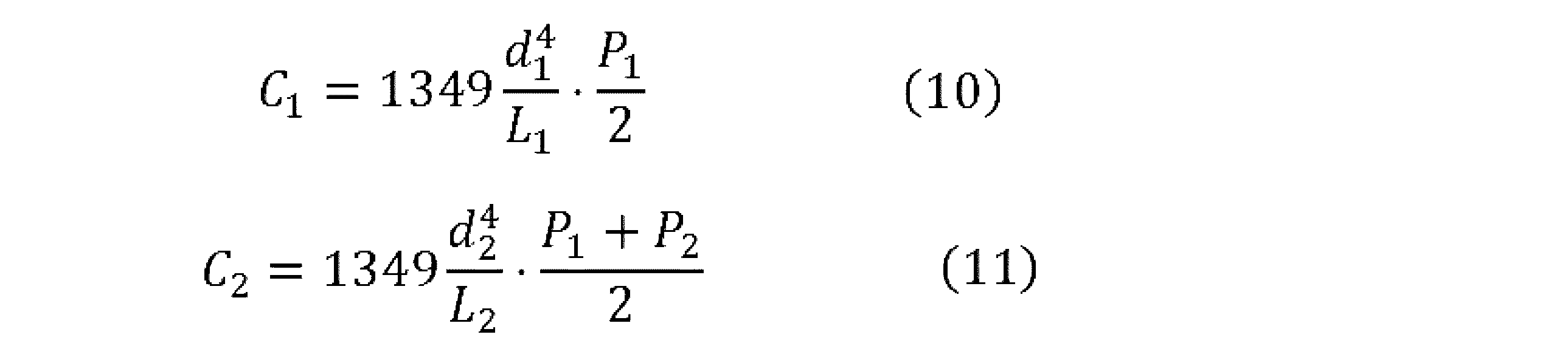
式(6)、(7)、(8)、(10)、(11)より下式が得られる。

式(1)~(5)、式(12)より、以下の関係式が得られる。

このような関係式を満たすように、各種仕様を決定すれば良い。例えば、L1=L2=5mm、R=200mm、c=25mm、d1=0.5mm、d2=0.7mm、n2を50個、n1が150個とした仕様では、式(13)の左辺は0.8であり、式(13)の関係式を満たす。すなわち、上記仕様で、上シャワープレート12の突起部12aと下シャワープレート13との密着性が保たれることがわかる。
上記のモデルではシャワープレートのガス孔形状を円筒としていたが、末広がりのノズル形状であっても良いし、ラバルノズル形状であっても良い。近似的に式(13)のd1とd2としてガス孔形状の最小径を代入して代用してもよい。
なお、本実施形態では上シャワープレート12と下シャワープレート13を同一材料として式(13)を導いたが、異種材料を用いる場合、そのヤング率、ポアソン比を用いて同様な手法で、上シャワープレート12の突起部12aと下シャワープレート13の密着性を確保する条件を導くことが出来る。
[第三の実施形態]
次に、第一の実施形態または第二の実施形態に係る構成に適用可能な、マイクロ波導入窓11と上シャワープレート12と下シャワープレート13の外周部の具体的構成について述べる。図7は、マイクロ波導入窓11と上シャワープレート12と下シャワープレート13外周部を拡大した図である。マイクロ波導入窓11と上シャワープレート12と下シャワープレート13の外周を支持する環状のヘッドピース(支持部材)26には、Oリング27が3本配置されている。
次に、第一の実施形態または第二の実施形態に係る構成に適用可能な、マイクロ波導入窓11と上シャワープレート12と下シャワープレート13の外周部の具体的構成について述べる。図7は、マイクロ波導入窓11と上シャワープレート12と下シャワープレート13外周部を拡大した図である。マイクロ波導入窓11と上シャワープレート12と下シャワープレート13の外周を支持する環状のヘッドピース(支持部材)26には、Oリング27が3本配置されている。
Oリング27の上に、マイクロ波導入窓11と、上シャワープレート12と、下シャワープレート13の外周部がそれぞれ載置される。ここで、マイクロ波導入窓11の外径は、上シャワープレート12の外径よりも大きく、且つ上シャワープレート12の外径は、下シャワープレート13の外径より大きいため、これらの外周部下面をOリング27を介して単一部材であるヘッドピース26により支持できる。
それぞれのOリング27の役割について説明する。マイクロ波導入窓11の外周部直下に位置するOリング27は、大気とのシール性を確保するために配置される。上シャワープレート12の外周部直下のOリング27は、第一と第二のガスが混合しないように配置される。そして、下シャワープレート13の外周部直下のOリング27は、第二のガスが下シャワープレート13とヘッドピース26間からプラズマ処理室100に漏れないようにするために配置される。
ヘッドピース26内部には、第一のガスと第二のガスが通るガス流路が形成されている。周方向に均一にガスを供給するために、上記ガス流路は周方向に複数本設けても良い。
図8Aは、マイクロ波導入窓11を下面側から見た図を示し、図8Bは、上シャワープレート12を下面側から見た図を示す。マイクロ波導入窓11と上シャワープレート12の下面中央には、円形凹部11aと円形凹部12bとがそれぞれ形成され、また外周近傍の下面には、ヘッドピース26のガス流路につながる周溝11bと周溝12cとがそれぞれ形成されている。周溝11b内を第一のガスが流れ、周溝12c内を第二のガスが流れる。
円形凹部11aと周溝11bとの間には、内側環状部11cが形成され、円形凹部12bと周溝12cとの間には、内側環状部12dが形成されている。また、周溝11bに隣接してその径方向外側には、外側環状部11dが形成され、周溝12cに隣接してその径方向外側には、外側環状部12eが形成されている。外周部である外側環状部11d、12eの下面は、Oリング27とのシール面である。
図7に示すように、マイクロ波導入窓11の内側環状部11cは、上シャワープレート12を押さえつける役割がある。また、上シャワープレート12の内側環状部12dも同様に、下シャワープレート13を押さえつける役割がある。これにより、Oリング27が弾性変形してガスのシール性が得られ、意図しない箇所へのガスの流出を防げる。また、ガスの圧力によって上シャワープレート12や下シャワープレート13の位置がずれることを防止できる。
図8Aに示すように、内側環状部11cには径方向に延在する複数の溝11eが形成されており、それにより円形凹部11aと周溝11bとを連通している。また図8Bに示すように、内側環状部12dには径方向に延在する複数の溝12fが形成されており、それにより円形凹部12bと周溝12cとを連通している。
内側環状部11c、12dに設けた複数の溝11e、12fは、周溝11b、12cに至った第一のガス及び第二のガスを、それぞれシャワープレートのガス孔に流す機能を有する。ガスを周方向において均等に行き渡らせるために、周方向に沿って溝が複数個所あることが望ましい。本実施形態では、内側環状部11c、12dには、それぞれ周方向に8箇所の溝11e、12fを配置している。
図9を参照して、マイクロ波導入窓11と、上シャワープレート12と、下シャワープレート13の外周部の別の例について述べる。本例では、図7の構成に対し、下シャワープレート13の外周面上部側に段差13aを設けている。第二のガス供給手段16から供給された第二のガスが、この段差13aとヘッドピース26とで画成される環状空間(第二の空間)を伝わって周方向に広がり、周方向に均一に下シャワープレート13のガス孔に導くことができる。それ以外の構成は上述した例と同様であるため、重複説明を省略する。
下シャワープレート13と同様に、上シャワープレート12外周面上部側にも段差を設けても良い。また、ガスを周方向に均一に行き渡らせるために、ヘッドピース26にガスを周方向に行き渡らせるための溝や段差部を設けてもよい。本実施形態では角形断面の環状空間を形成する段差13aを設けたが、段差の形状は任意である。
図10を参照して、マイクロ波導入窓11と上シャワープレート12と下シャワープレート13外周部の別の例について述べる。本例では、図7の構成に対し、下シャワープレート13外周部直下のOリングと、上シャワープレート12の周溝及び環状部を省略し、下シャワープレート13の下面全体を同一面とした構造である。すなわち、マイクロ波導入窓11と上シャワープレート12の外周部下面のみが、Oリング27を介してヘッドピース26により支持される。それ以外の構成は上述した例と同様であるため、重複説明を省略する。
通常、プロセス処理室内は真空であり、それに比べると上シャワープレート12と下シャワープレート13間の空間内は高い圧力となる。この圧力差により、上シャワープレート12の環状部で下シャワープレート13を押し付けなくても、ヘッドピース26と下シャワープレート13の外周部下面が密着する。このため、下シャワープレート13外周部直下のOリングを省略できる。これにより、上シャワープレート12と下シャワープレート13の形状を単純な円板とすることができ、製作が容易となる。
図11にてマイクロ波導入窓11と上シャワープレート12と下シャワープレート13外周部の別の例について述べる。本例によれば、図7の構成に対し、下シャワープレート13の外周面上部に、径方向に比較的幅のある段差13aを形成しており、この段差13aに収容するようにして、上シャワープレート12と下シャワープレート13とに当接するリング状のスペーサ28を設けている。
図10及び図11の例は、マイクロ波導入窓11の上方の大気側から処理室内部の状態を光学的にモニタリングしたい場合に有用な構造である。装置外方から光学カメラでプラズマ処理室100内部の状態を監視するためには、マイクロ波導入窓11、上シャワープレート12、下シャワープレート13を透明とする必要がある。そこで、マイクロ波導入窓11、上シャワープレート12、下シャワープレート13に、石英を用いる場合について検討する。
一般に、石英を切削加工しただけでは、表面粗さが大きくなり光が乱反射して不透明となるから、追加で透明化処理が必要である。石英を透明化する手法は大きく分けて、機械的な研磨と、火炎で表面を溶融するファイアポリッシュがある。機械的な研磨は対象が単純な平面であれば良好な平面度を実現できるものの、周溝や段差があり、くぼんでいる面に対しては研磨加工が困難である。
これに対し、ファイアポリッシュによって透明化する場合、部材が熱によって変形するため、面精度が悪くなりやすいという課題がある。しかし、マイクロ波導入窓11は大気圧に耐える強度を持たせるため、通常30mm以上と厚みを有する。このように部材が厚い場合は熱による変形量が小さく、ファイアポリッシュを実施しても平面度50μm以下とでき、工業製品として許容できる低い公差を確保しながら透明化できる。
一方で、シャワープレートはレーザ加工でガス孔を形成しやすい厚さとして10mm以下に薄くすることが多い。このように部材が薄い場合は熱による変形量が大きいため、ファイアポリッシュ後の平面度は数百μm以上と粗くなってしまう。上シャワープレート12と下シャワープレート13間はガスが通る流路となっているため、平面度が悪い場合、ガスの流れる空間が部分的に狭くなってガス流れが偏ってしまい、プラズマエッチング処理において許容できない場合がある。そこで、上シャワープレート12や下シャワープレート13を透明化するためには、機械研磨が望ましい。これに対し、図10及び図11の構成では、上シャワープレート12と下シャワープレート13の上下面がフラットな平板状であるため、機械研磨による透明化が可能となる。
なお、本発明は上記した実施の形態に限定されるものではなく、様々な変形例が含まれる。例えば、上記した実施の形態は本発明を分かりやすく説明するために詳細に説明したものであり、必ずしも説明した全ての構成を備えるものに限定されるものではない。また、ある実施の形態における構成の一部を他の実施の形態の構成に置き換えることが可能であり、また、ある実施の形態の構成に他の実施の形態の構成を加えることも可能である。また、各実施の形態における構成の一部について、他の構成の追加・削除・置換をすることも可能である。
本発明は、半導体ウエハ等の基板上の試料をエッチング等で処理するプラズマ処理装置に適用可能である。
1 マイクロ波源、2 方形導波管、3 自動整合機、4 アイソレータ、5 円矩形変換器、6 円形導波管、7 空洞部、8 電磁コイル、9 ヨーク、10 被処理基板、11 マイクロ波導入窓、12 上シャワープレート、13 下シャワープレート、14 内筒、15 第一のガス供給手段、16 第二のガス供給手段、17 基板ステージ兼高周波電極、18 絶縁板、19 コンダクタンス調節バルブ、20 ターボ分子ポンプ、21 バイアス用自動整合機、22 バイアス電源、23 サセプタ、24 カバーリング、25 チャンバ内壁、26 ヘッドピース、27 Oリング、28 スペーサ、100 プラズマ処理室、101 プラズマ
Claims (12)
- 試料がプラズマ処理される処理室と、プラズマを生成するための高周波電力を供給する高周波電源と、前記処理室の上方に配置され前記処理室を気密に封止する誘電体板と、前記誘電体板の下方に配置され第一のガスを前記処理室内へ供給する第一のガス供給板と、前記試料が載置される試料台とを備えるプラズマ処理装置において、
前記第一のガス供給板の下方に配置され第二のガスを前記処理室内へ供給する第二のガス供給板をさらに備え、
前記第一のガス供給板には、第一のガス孔が第一の領域に貫通して複数個形成されており、
前記第二のガス供給板には、第二のガス孔が第二の領域に貫通して複数個形成されており、
前記誘電体板と前記第一のガス供給板の間の空間には、第一のガス供給手段により前記第一のガスが供給され、
前記第一のガス供給板と前記第二のガス供給板の間の空間には、第二のガス供給手段により前記第二のガスが供給され、
前記第一の領域は、前記第一のガス供給板の中央部の領域であり、
前記第二の領域は、前記第一の領域を含むとともに前記第一の領域より広い領域であることを特徴とするプラズマ処理装置。 - 請求項1に記載のプラズマ処理装置において、
前記第二のガス孔の各々のコンダクタンスは、前記第一のガス孔の各々のコンダクタンスよりも大きいことを特徴とするプラズマ処理装置。 - 請求項1または請求項2に記載のプラズマ処理装置において、
前記処理室内の径方向のガス流れを概ね均一にする場合、前記第二のガスの流量が前記第一のガスの流量より大きくなるように前記第一のガス供給手段と前記第二のガス供給手段を制御する制御装置をさらに備えることを特徴とするプラズマ処理装置。 - 請求項1に記載のプラズマ処理装置において、
前記第一のガス供給板と前記第二のガス供給板の間の空間は、第一の空間と第二の空間により構成され、
前記第一の空間は、前記誘電体板と前記第一のガス供給板の間の空間に対向し、
前記第二の空間は、前記第一の空間より外側に位置し、
前記第二のガス供給板には、第三のガス孔が貫通して前記第二の空間内に複数個形成されており、
前記誘電体板と前記第一のガス供給板の間の空間に供給された第一のガスは、前記第一の空間、前記第一のガス孔および前記第二のガス孔を介して前記処理室内へ供給され、
前記第二の空間に供給された第二のガスは、前記第三のガス孔を介して前記処理室内へ供給されることを特徴とするプラズマ処理装置。 - 請求項4に記載のプラズマ処理装置において、
前記第一のガス孔の各々のコンダクタンスにおける総和は、前記第二のガス孔の各々のコンダクタンスにおける総和よりも小さいことを特徴とするプラズマ処理装置。 - 請求項1ないし請求項5のいずれか一項に記載のプラズマ処理装置において、
前記誘電体板の外径は、前記第一のガス供給板の外径よりも大きく、
前記第一のガス供給板の外径は、前記第二のガス供給板の外径より大きいことを特徴とするプラズマ処理装置。 - 請求項1ないし請求項6のいずれか一項に記載のプラズマ処理装置において、
前記誘電体板と前記第一ガス供給板と前記第二のガス供給板の各々の外周部下面は、Oリングを介して環状の支持部材の上に配置されることを特徴とするプラズマ処理装置。 - 請求項1ないし請求項6のいずれか一項に記載のプラズマ処理装置において、
前記誘電体板と前記第一のガス供給板の各々の外周部下面は、Oリングを介して環状の支持部材の上に配置され、
前記第二のガス供給板の外周部下面は、前記支持部材と接するように配置されることを特徴とするプラズマ処理装置。 - 請求項7または請求項8に記載のプラズマ処理装置において、
前記第一のガスが流れる溝が前記誘電体板の下面に形成され、
前記第二のガスが流れる溝が前記第一のガス供給板の下面に形成されたことを特徴とするプラズマ処理装置。 - 請求項9に記載のプラズマ処理装置において、
前記第二の空間を画成する段差が前記第二のガス供給板の外周面に形成されたことを特徴とするプラズマ処理装置。 - 請求項10に記載のプラズマ処理装置において、
前記第一のガス供給板に当接するスペーサが前記段差に配置されたことを特徴とするプラズマ処理装置。 - 請求項7ないし請求項11のいずれか一項に記載のプラズマ処理装置において、
前記第一のガス供給板と前記第二のガス供給板の材質は石英であることを特徴とするプラズマ処理装置。
Priority Applications (6)
| Application Number | Priority Date | Filing Date | Title |
|---|---|---|---|
| US16/958,313 US12014903B2 (en) | 2019-07-18 | 2019-07-18 | Plasma processing apparatus |
| KR1020207009884A KR102409660B1 (ko) | 2019-07-18 | 2019-07-18 | 플라스마 처리 장치 |
| JP2020520671A JP6987986B2 (ja) | 2019-07-18 | 2019-07-18 | プラズマ処理装置 |
| CN201980005164.4A CN112534552B (zh) | 2019-07-18 | 2019-07-18 | 等离子处理装置 |
| PCT/JP2019/028262 WO2020121581A1 (ja) | 2019-07-18 | 2019-07-18 | プラズマ処理装置 |
| TW109114145A TWI756670B (zh) | 2019-07-18 | 2020-04-28 | 電漿處理裝置 |
Applications Claiming Priority (1)
| Application Number | Priority Date | Filing Date | Title |
|---|---|---|---|
| PCT/JP2019/028262 WO2020121581A1 (ja) | 2019-07-18 | 2019-07-18 | プラズマ処理装置 |
Publications (1)
| Publication Number | Publication Date |
|---|---|
| WO2020121581A1 true WO2020121581A1 (ja) | 2020-06-18 |
Family
ID=71076599
Family Applications (1)
| Application Number | Title | Priority Date | Filing Date |
|---|---|---|---|
| PCT/JP2019/028262 Ceased WO2020121581A1 (ja) | 2019-07-18 | 2019-07-18 | プラズマ処理装置 |
Country Status (6)
| Country | Link |
|---|---|
| US (1) | US12014903B2 (ja) |
| JP (1) | JP6987986B2 (ja) |
| KR (1) | KR102409660B1 (ja) |
| CN (1) | CN112534552B (ja) |
| TW (1) | TWI756670B (ja) |
| WO (1) | WO2020121581A1 (ja) |
Cited By (2)
| Publication number | Priority date | Publication date | Assignee | Title |
|---|---|---|---|---|
| JP2022006424A (ja) * | 2020-06-24 | 2022-01-13 | 株式会社日立ハイテク | プラズマ処理装置 |
| WO2026059724A1 (en) * | 2024-09-13 | 2026-03-19 | Lam Research Corporation | Cover ring for rf return path |
Families Citing this family (3)
| Publication number | Priority date | Publication date | Assignee | Title |
|---|---|---|---|---|
| KR20240072995A (ko) * | 2021-08-04 | 2024-05-24 | 도쿄엘렉트론가부시키가이샤 | 플라스마 처리 장치 |
| CN115799061B (zh) * | 2023-01-09 | 2023-09-05 | 浙江大学杭州国际科创中心 | SiC晶圆切割片加工方法及SiC晶圆切割片加工装置 |
| CN118136485B (zh) * | 2024-05-08 | 2024-08-27 | 上海谙邦半导体设备有限公司 | 一种进气装置及等离子刻蚀机 |
Citations (4)
| Publication number | Priority date | Publication date | Assignee | Title |
|---|---|---|---|---|
| JPH11172448A (ja) * | 1997-12-12 | 1999-06-29 | Tadahiro Omi | 光学部品の製造法 |
| JP2004022595A (ja) * | 2002-06-12 | 2004-01-22 | Toshiba Corp | 絶縁膜の製造方法、およびプラズマcvd装置 |
| JP2006324400A (ja) * | 2005-05-18 | 2006-11-30 | Shimadzu Corp | シャワーヘッドおよび表面波励起プラズマ処理装置 |
| JP2015532016A (ja) * | 2012-09-21 | 2015-11-05 | アプライド マテリアルズ インコーポレイテッドApplied Materials,Incorporated | ラジカルの化学的性質の複数の流れ経路を使用した調節及び制御 |
Family Cites Families (14)
| Publication number | Priority date | Publication date | Assignee | Title |
|---|---|---|---|---|
| JP3535309B2 (ja) * | 1996-04-10 | 2004-06-07 | 東京エレクトロン株式会社 | 減圧処理装置 |
| WO1998033362A1 (en) * | 1997-01-29 | 1998-07-30 | Tadahiro Ohmi | Plasma device |
| TWI423308B (zh) | 2005-09-01 | 2014-01-11 | 松下電器產業股份有限公司 | A plasma processing apparatus, a plasma processing method, and a dielectric window for use therefor and a method of manufacturing the same |
| JP2007242777A (ja) | 2006-03-07 | 2007-09-20 | Hitachi High-Technologies Corp | プラズマエッチング装置及びプラズマエッチング方法 |
| CN102089867B (zh) * | 2008-07-11 | 2013-11-27 | 东京毅力科创株式会社 | 等离子体处理装置 |
| WO2010079766A1 (ja) * | 2009-01-09 | 2010-07-15 | 株式会社アルバック | プラズマ処理装置 |
| JP2010278207A (ja) * | 2009-05-28 | 2010-12-09 | Hitachi High-Technologies Corp | プラズマ処理装置 |
| WO2012060423A1 (ja) | 2010-11-05 | 2012-05-10 | 株式会社アルバック | ラジカルクリーニング装置及び方法 |
| JP2013131587A (ja) | 2011-12-21 | 2013-07-04 | Hitachi High-Technologies Corp | プラズマ処理方法 |
| US10249511B2 (en) * | 2014-06-27 | 2019-04-02 | Lam Research Corporation | Ceramic showerhead including central gas injector for tunable convective-diffusive gas flow in semiconductor substrate processing apparatus |
| JP2016136553A (ja) | 2015-01-23 | 2016-07-28 | 株式会社日立ハイテクノロジーズ | プラズマ処理装置 |
| JP6488164B2 (ja) * | 2015-03-23 | 2019-03-20 | 株式会社日立ハイテクノロジーズ | プラズマ処理装置 |
| US10546729B2 (en) | 2016-10-04 | 2020-01-28 | Applied Materials, Inc. | Dual-channel showerhead with improved profile |
| JP7085828B2 (ja) * | 2017-12-18 | 2022-06-17 | 株式会社日立ハイテク | プラズマ処理装置 |
-
2019
- 2019-07-18 CN CN201980005164.4A patent/CN112534552B/zh active Active
- 2019-07-18 US US16/958,313 patent/US12014903B2/en active Active
- 2019-07-18 JP JP2020520671A patent/JP6987986B2/ja active Active
- 2019-07-18 KR KR1020207009884A patent/KR102409660B1/ko not_active Expired - Fee Related
- 2019-07-18 WO PCT/JP2019/028262 patent/WO2020121581A1/ja not_active Ceased
-
2020
- 2020-04-28 TW TW109114145A patent/TWI756670B/zh active
Patent Citations (4)
| Publication number | Priority date | Publication date | Assignee | Title |
|---|---|---|---|---|
| JPH11172448A (ja) * | 1997-12-12 | 1999-06-29 | Tadahiro Omi | 光学部品の製造法 |
| JP2004022595A (ja) * | 2002-06-12 | 2004-01-22 | Toshiba Corp | 絶縁膜の製造方法、およびプラズマcvd装置 |
| JP2006324400A (ja) * | 2005-05-18 | 2006-11-30 | Shimadzu Corp | シャワーヘッドおよび表面波励起プラズマ処理装置 |
| JP2015532016A (ja) * | 2012-09-21 | 2015-11-05 | アプライド マテリアルズ インコーポレイテッドApplied Materials,Incorporated | ラジカルの化学的性質の複数の流れ経路を使用した調節及び制御 |
Cited By (3)
| Publication number | Priority date | Publication date | Assignee | Title |
|---|---|---|---|---|
| JP2022006424A (ja) * | 2020-06-24 | 2022-01-13 | 株式会社日立ハイテク | プラズマ処理装置 |
| JP7281433B2 (ja) | 2020-06-24 | 2023-05-25 | 株式会社日立ハイテク | プラズマ処理装置 |
| WO2026059724A1 (en) * | 2024-09-13 | 2026-03-19 | Lam Research Corporation | Cover ring for rf return path |
Also Published As
| Publication number | Publication date |
|---|---|
| US20220415618A1 (en) | 2022-12-29 |
| TW202105510A (zh) | 2021-02-01 |
| TWI756670B (zh) | 2022-03-01 |
| CN112534552A (zh) | 2021-03-19 |
| JP6987986B2 (ja) | 2022-01-05 |
| US12014903B2 (en) | 2024-06-18 |
| KR102409660B1 (ko) | 2022-06-22 |
| JPWO2020121581A1 (ja) | 2021-02-15 |
| CN112534552B (zh) | 2024-04-12 |
| KR20210010425A (ko) | 2021-01-27 |
Similar Documents
| Publication | Publication Date | Title |
|---|---|---|
| JP6987986B2 (ja) | プラズマ処理装置 | |
| JP4833469B2 (ja) | 面積の大きな基板の処理のためのプラズマ反応装置 | |
| US20120145186A1 (en) | Plasma processing apparatus | |
| US20040040931A1 (en) | Plasma processing method and plasma processor | |
| US20020187647A1 (en) | Stepped upper electrode for plasma processing uniformity | |
| US8529730B2 (en) | Plasma processing apparatus | |
| KR20120015280A (ko) | 플라즈마 처리 장치 및 플라즈마 제어 방법 | |
| US20150155139A1 (en) | Dielectric window, antenna and plasma processing apparatus | |
| JP2012049376A (ja) | プラズマ処理装置およびプラズマ処理方法 | |
| JPWO2002058125A1 (ja) | プラズマ処理装置およびプラズマ処理方法 | |
| KR100579606B1 (ko) | 플라즈마 처리방법 및 플라즈마 처리장치 | |
| CN115398602A (zh) | 等离子处理装置以及等离子处理方法 | |
| JP7001456B2 (ja) | プラズマ処理装置 | |
| CN110770880B (zh) | 等离子处理装置 | |
| KR102229990B1 (ko) | 플라즈마 처리 장치용 부재 및 플라즈마 처리 장치 | |
| JP7281433B2 (ja) | プラズマ処理装置 | |
| TWI830148B (zh) | 電漿處理裝置 | |
| JP2005079416A (ja) | プラズマ処理装置 | |
| JP7228392B2 (ja) | プラズマ処理装置 | |
| JP5670245B2 (ja) | プラズマ処理装置 | |
| JP3364131B2 (ja) | プラズマ処理装置 | |
| JP4832222B2 (ja) | プラズマ処理装置 | |
| JP7587056B2 (ja) | 内壁部材の再生方法 | |
| US20020168814A1 (en) | Plasma processing method and apparatus | |
| JP2012134235A (ja) | プラズマ処理装置 |
Legal Events
| Date | Code | Title | Description |
|---|---|---|---|
| ENP | Entry into the national phase |
Ref document number: 2020520671 Country of ref document: JP Kind code of ref document: A |
|
| 121 | Ep: the epo has been informed by wipo that ep was designated in this application |
Ref document number: 19896197 Country of ref document: EP Kind code of ref document: A1 |
|
| NENP | Non-entry into the national phase |
Ref country code: DE |
|
| 122 | Ep: pct application non-entry in european phase |
Ref document number: 19896197 Country of ref document: EP Kind code of ref document: A1 |