WO2020115952A1 - 静電チャック、真空処理装置及び基板処理方法 - Google Patents
静電チャック、真空処理装置及び基板処理方法 Download PDFInfo
- Publication number
- WO2020115952A1 WO2020115952A1 PCT/JP2019/031443 JP2019031443W WO2020115952A1 WO 2020115952 A1 WO2020115952 A1 WO 2020115952A1 JP 2019031443 W JP2019031443 W JP 2019031443W WO 2020115952 A1 WO2020115952 A1 WO 2020115952A1
- Authority
- WO
- WIPO (PCT)
- Prior art keywords
- substrate
- chuck
- electrostatic chuck
- chuck plate
- electrostatic
- Prior art date
- Legal status (The legal status is an assumption and is not a legal conclusion. Google has not performed a legal analysis and makes no representation as to the accuracy of the status listed.)
- Ceased
Links
Images



Classifications
-
- H—ELECTRICITY
- H10—SEMICONDUCTOR DEVICES; ELECTRIC SOLID-STATE DEVICES NOT OTHERWISE PROVIDED FOR
- H10P—GENERIC PROCESSES OR APPARATUS FOR THE MANUFACTURE OR TREATMENT OF DEVICES COVERED BY CLASS H10
- H10P72/00—Handling or holding of wafers, substrates or devices during manufacture or treatment thereof
- H10P72/04—Apparatus for manufacture or treatment
- H10P72/0402—Apparatus for fluid treatment
-
- H—ELECTRICITY
- H10—SEMICONDUCTOR DEVICES; ELECTRIC SOLID-STATE DEVICES NOT OTHERWISE PROVIDED FOR
- H10P—GENERIC PROCESSES OR APPARATUS FOR THE MANUFACTURE OR TREATMENT OF DEVICES COVERED BY CLASS H10
- H10P72/00—Handling or holding of wafers, substrates or devices during manufacture or treatment thereof
- H10P72/70—Handling or holding of wafers, substrates or devices during manufacture or treatment thereof for supporting or gripping
- H10P72/72—Handling or holding of wafers, substrates or devices during manufacture or treatment thereof for supporting or gripping using electrostatic chucks
- H10P72/722—Details of electrostatic chucks
-
- C—CHEMISTRY; METALLURGY
- C23—COATING METALLIC MATERIAL; COATING MATERIAL WITH METALLIC MATERIAL; CHEMICAL SURFACE TREATMENT; DIFFUSION TREATMENT OF METALLIC MATERIAL; COATING BY VACUUM EVAPORATION, BY SPUTTERING, BY ION IMPLANTATION OR BY CHEMICAL VAPOUR DEPOSITION, IN GENERAL; INHIBITING CORROSION OF METALLIC MATERIAL OR INCRUSTATION IN GENERAL
- C23C—COATING METALLIC MATERIAL; COATING MATERIAL WITH METALLIC MATERIAL; SURFACE TREATMENT OF METALLIC MATERIAL BY DIFFUSION INTO THE SURFACE, BY CHEMICAL CONVERSION OR SUBSTITUTION; COATING BY VACUUM EVAPORATION, BY SPUTTERING, BY ION IMPLANTATION OR BY CHEMICAL VAPOUR DEPOSITION, IN GENERAL
- C23C14/00—Coating by vacuum evaporation, by sputtering or by ion implantation of the coating forming material
- C23C14/22—Coating by vacuum evaporation, by sputtering or by ion implantation of the coating forming material characterised by the process of coating
- C23C14/48—Ion implantation
-
- C—CHEMISTRY; METALLURGY
- C23—COATING METALLIC MATERIAL; COATING MATERIAL WITH METALLIC MATERIAL; CHEMICAL SURFACE TREATMENT; DIFFUSION TREATMENT OF METALLIC MATERIAL; COATING BY VACUUM EVAPORATION, BY SPUTTERING, BY ION IMPLANTATION OR BY CHEMICAL VAPOUR DEPOSITION, IN GENERAL; INHIBITING CORROSION OF METALLIC MATERIAL OR INCRUSTATION IN GENERAL
- C23C—COATING METALLIC MATERIAL; COATING MATERIAL WITH METALLIC MATERIAL; SURFACE TREATMENT OF METALLIC MATERIAL BY DIFFUSION INTO THE SURFACE, BY CHEMICAL CONVERSION OR SUBSTITUTION; COATING BY VACUUM EVAPORATION, BY SPUTTERING, BY ION IMPLANTATION OR BY CHEMICAL VAPOUR DEPOSITION, IN GENERAL
- C23C14/00—Coating by vacuum evaporation, by sputtering or by ion implantation of the coating forming material
- C23C14/22—Coating by vacuum evaporation, by sputtering or by ion implantation of the coating forming material characterised by the process of coating
- C23C14/50—Substrate holders
-
- C—CHEMISTRY; METALLURGY
- C23—COATING METALLIC MATERIAL; COATING MATERIAL WITH METALLIC MATERIAL; CHEMICAL SURFACE TREATMENT; DIFFUSION TREATMENT OF METALLIC MATERIAL; COATING BY VACUUM EVAPORATION, BY SPUTTERING, BY ION IMPLANTATION OR BY CHEMICAL VAPOUR DEPOSITION, IN GENERAL; INHIBITING CORROSION OF METALLIC MATERIAL OR INCRUSTATION IN GENERAL
- C23C—COATING METALLIC MATERIAL; COATING MATERIAL WITH METALLIC MATERIAL; SURFACE TREATMENT OF METALLIC MATERIAL BY DIFFUSION INTO THE SURFACE, BY CHEMICAL CONVERSION OR SUBSTITUTION; COATING BY VACUUM EVAPORATION, BY SPUTTERING, BY ION IMPLANTATION OR BY CHEMICAL VAPOUR DEPOSITION, IN GENERAL
- C23C16/00—Chemical coating by decomposition of gaseous compounds, without leaving reaction products of surface material in the coating, i.e. chemical vapour deposition [CVD] processes
- C23C16/44—Chemical coating by decomposition of gaseous compounds, without leaving reaction products of surface material in the coating, i.e. chemical vapour deposition [CVD] processes characterised by the method of coating
- C23C16/458—Chemical coating by decomposition of gaseous compounds, without leaving reaction products of surface material in the coating, i.e. chemical vapour deposition [CVD] processes characterised by the method of coating characterised by the method used for supporting substrates in the reaction chamber
- C23C16/4582—Rigid and flat substrates, e.g. plates or discs
- C23C16/4583—Rigid and flat substrates, e.g. plates or discs the substrate being supported substantially horizontally
- C23C16/4586—Elements in the interior of the support, e.g. electrodes, heating or cooling devices
-
- H—ELECTRICITY
- H01—ELECTRIC ELEMENTS
- H01J—ELECTRIC DISCHARGE TUBES OR DISCHARGE LAMPS
- H01J37/00—Discharge tubes with provision for introducing objects or material to be exposed to the discharge, e.g. for the purpose of examination or processing thereof
- H01J37/30—Electron-beam or ion-beam tubes for localised treatment of objects
- H01J37/317—Electron-beam or ion-beam tubes for localised treatment of objects for changing properties of the objects or for applying thin layers thereon, e.g. for ion implantation
- H01J37/3171—Electron-beam or ion-beam tubes for localised treatment of objects for changing properties of the objects or for applying thin layers thereon, e.g. for ion implantation for ion implantation
-
- H—ELECTRICITY
- H10—SEMICONDUCTOR DEVICES; ELECTRIC SOLID-STATE DEVICES NOT OTHERWISE PROVIDED FOR
- H10P—GENERIC PROCESSES OR APPARATUS FOR THE MANUFACTURE OR TREATMENT OF DEVICES COVERED BY CLASS H10
- H10P14/00—Formation of materials, e.g. in the shape of layers or pillars
- H10P14/60—Formation of materials, e.g. in the shape of layers or pillars of insulating materials
-
- H—ELECTRICITY
- H10—SEMICONDUCTOR DEVICES; ELECTRIC SOLID-STATE DEVICES NOT OTHERWISE PROVIDED FOR
- H10P—GENERIC PROCESSES OR APPARATUS FOR THE MANUFACTURE OR TREATMENT OF DEVICES COVERED BY CLASS H10
- H10P50/00—Etching of wafers, substrates or parts of devices
- H10P50/20—Dry etching; Plasma etching; Reactive-ion etching
- H10P50/24—Dry etching; Plasma etching; Reactive-ion etching of semiconductor materials
- H10P50/242—Dry etching; Plasma etching; Reactive-ion etching of semiconductor materials of Group IV materials
-
- H—ELECTRICITY
- H10—SEMICONDUCTOR DEVICES; ELECTRIC SOLID-STATE DEVICES NOT OTHERWISE PROVIDED FOR
- H10P—GENERIC PROCESSES OR APPARATUS FOR THE MANUFACTURE OR TREATMENT OF DEVICES COVERED BY CLASS H10
- H10P72/00—Handling or holding of wafers, substrates or devices during manufacture or treatment thereof
- H10P72/04—Apparatus for manufacture or treatment
- H10P72/0451—Apparatus for manufacturing or treating in a plurality of work-stations
- H10P72/0468—Apparatus for manufacturing or treating in a plurality of work-stations comprising a chamber adapted to a particular process
- H10P72/0471—Apparatus for manufacturing or treating in a plurality of work-stations comprising a chamber adapted to a particular process comprising at least one ion or electron beam chamber
-
- H—ELECTRICITY
- H10—SEMICONDUCTOR DEVICES; ELECTRIC SOLID-STATE DEVICES NOT OTHERWISE PROVIDED FOR
- H10P—GENERIC PROCESSES OR APPARATUS FOR THE MANUFACTURE OR TREATMENT OF DEVICES COVERED BY CLASS H10
- H10P72/00—Handling or holding of wafers, substrates or devices during manufacture or treatment thereof
- H10P72/70—Handling or holding of wafers, substrates or devices during manufacture or treatment thereof for supporting or gripping
- H10P72/72—Handling or holding of wafers, substrates or devices during manufacture or treatment thereof for supporting or gripping using electrostatic chucks
-
- H—ELECTRICITY
- H10—SEMICONDUCTOR DEVICES; ELECTRIC SOLID-STATE DEVICES NOT OTHERWISE PROVIDED FOR
- H10P—GENERIC PROCESSES OR APPARATUS FOR THE MANUFACTURE OR TREATMENT OF DEVICES COVERED BY CLASS H10
- H10P72/00—Handling or holding of wafers, substrates or devices during manufacture or treatment thereof
- H10P72/70—Handling or holding of wafers, substrates or devices during manufacture or treatment thereof for supporting or gripping
- H10P72/76—Handling or holding of wafers, substrates or devices during manufacture or treatment thereof for supporting or gripping using mechanical means, e.g. clamps or pinches
- H10P72/7604—Handling or holding of wafers, substrates or devices during manufacture or treatment thereof for supporting or gripping using mechanical means, e.g. clamps or pinches the wafers being placed on a susceptor, stage or support
- H10P72/7614—Handling or holding of wafers, substrates or devices during manufacture or treatment thereof for supporting or gripping using mechanical means, e.g. clamps or pinches the wafers being placed on a susceptor, stage or support characterised by a plurality of individual support members, e.g. support posts or protrusions
-
- H—ELECTRICITY
- H10—SEMICONDUCTOR DEVICES; ELECTRIC SOLID-STATE DEVICES NOT OTHERWISE PROVIDED FOR
- H10P—GENERIC PROCESSES OR APPARATUS FOR THE MANUFACTURE OR TREATMENT OF DEVICES COVERED BY CLASS H10
- H10P72/00—Handling or holding of wafers, substrates or devices during manufacture or treatment thereof
- H10P72/70—Handling or holding of wafers, substrates or devices during manufacture or treatment thereof for supporting or gripping
- H10P72/76—Handling or holding of wafers, substrates or devices during manufacture or treatment thereof for supporting or gripping using mechanical means, e.g. clamps or pinches
- H10P72/7604—Handling or holding of wafers, substrates or devices during manufacture or treatment thereof for supporting or gripping using mechanical means, e.g. clamps or pinches the wafers being placed on a susceptor, stage or support
- H10P72/7624—Handling or holding of wafers, substrates or devices during manufacture or treatment thereof for supporting or gripping using mechanical means, e.g. clamps or pinches the wafers being placed on a susceptor, stage or support characterised by the mechanical construction of the susceptor, stage or support
-
- H—ELECTRICITY
- H10—SEMICONDUCTOR DEVICES; ELECTRIC SOLID-STATE DEVICES NOT OTHERWISE PROVIDED FOR
- H10P—GENERIC PROCESSES OR APPARATUS FOR THE MANUFACTURE OR TREATMENT OF DEVICES COVERED BY CLASS H10
- H10P30/00—Ion implantation into wafers, substrates or parts of devices
- H10P30/20—Ion implantation into wafers, substrates or parts of devices into semiconductor materials, e.g. for doping
Definitions
- the present invention relates to an electrostatic chuck, a vacuum processing apparatus, and a substrate processing method.
- the substrate that is the base material of the electronic component is supported on the stage in a reduced pressure atmosphere, and process processes such as film formation, etching, and ion implantation are performed.
- the process processing is performed, for example, in a state where the substrate is attracted to the electrostatic chuck (see, for example, Patent Document 1).
- the substrate may be warmed by the processing, and gas may accumulate between the electrostatic chuck and the substrate. If electrostatic attraction is released in such a state, a phenomenon may occur in which the substrate jumps up from the electrostatic chuck due to a rapid increase in volume of residual gas.
- an object of the present invention is to provide an electrostatic chuck, a vacuum processing apparatus, and a substrate processing method that suppress a rapid volume increase of the gas and stably support a substrate.
- an electrostatic chuck includes a chuck plate having a first surface supporting a substrate and a second surface opposite to the first surface.
- the chuck plate has exhaust gas for exhausting gas emitted from the substrate between the substrate and the first surface when the substrate is supported by the first surface, between the substrate and the first surface.
- an exhaust path for exhausting the gas emitted from the substrate between the substrate and the first surface is provided between the substrate and the first surface. Since it is provided, rapid volume expansion of the gas is suppressed even if electrostatic attraction is released, and jumping of the substrate from the chuck plate can be prevented.
- the exhaust passage has a groove provided on the first surface and a first through hole communicating with the groove and penetrating from the first surface to the second surface. Good.
- the exhaust path has the groove provided on the first surface and the first through hole communicating with the groove and penetrating from the first surface to the second surface, The gas released from the substrate is efficiently exhausted to the second surface side through the exhaust passage.
- the groove intersects a plurality of first groove portions extending in a direction from the center of the chuck plate toward the outside of the chuck plate, and the plurality of first groove portions, and You may have several 2nd groove part formed in the cyclic
- the groove has a plurality of first groove portions extending from the center of the chuck plate toward the outside of the chuck plate, and a plurality of second groove portions formed in an annular shape. Therefore, the gas released from the substrate is efficiently exhausted to the second surface side through the groove.
- the exhaust passage may have a linear bank portion provided on the first surface and a first through hole penetrating from the first surface to the second surface. ..
- the exhaust path since the exhaust path has the bank portion provided on the first surface and the first through hole penetrating from the first surface to the second surface, the exhaust path is discharged from the substrate. Gas is efficiently exhausted to the second surface side through the exhaust passage.
- a plurality of convex portions and an annular convex portion surrounding the plurality of convex portions are provided on the first surface, and the height of the plurality of convex portions from the first surface is the above.
- the height may be less than or equal to the height of the annular protrusion.
- the convex embossing is applied to the first surface, the gas released from the substrate efficiently passes through the first surface to the second surface side through the exhaust passage. Exhausted. Further, the annular convex portion makes it difficult for gas to leak from between the substrate and the chuck plate.
- the electrostatic chuck may further include a chuck base having a third surface facing the second surface of the chuck plate and a fourth surface opposite to the third surface.
- the chuck base may be provided with a second through hole penetrating from the third surface to the fourth surface, and the second through hole may be configured to communicate with the first through hole.
- the chuck base having the third surface facing the second surface of the chuck plate and the fourth surface opposite to the third surface, from the third surface to the fourth surface. Since the second through hole that penetrates is provided, the gas released from the substrate is efficiently exhausted to the fourth surface side through the exhaust passage.
- a vacuum processing apparatus includes a vacuum container, the electrostatic chuck, a support base, and a deposition preventive plate.
- the support base is housed in the vacuum container and has a fifth surface for supporting the electrostatic chuck, and a sixth surface opposite to the fifth surface.
- the deposition preventive plate surrounds the support table and partitions the interior of the vacuum container into a first area in which the electrostatic chuck is arranged and a second area in which the support table is arranged.
- the support base is provided with another exhaust passage for exhausting the gas introduced through the exhaust passage to the second region.
- the electrostatic chuck is prepared.
- the substrate is placed on the first surface having a plurality of convex portions formed by convex embossing.
- the height h 0 of the plurality of convex portions from the first surface is the height h 0.
- the height h 1 is adjusted to be lower than 0 .
- the substrate is processed. By mitigating the electrostatic adsorption, the gas generated during the process processing is exhausted from between the substrate and the first surface.
- an exhaust path for exhausting the gas emitted from the substrate between the substrate and the first surface is provided between the substrate and the first surface. Since it is provided, rapid volume expansion of the gas is suppressed even if electrostatic attraction is released, and jumping of the substrate from the chuck plate can be prevented.
- an electrostatic chuck As described above, according to the present invention, there are provided an electrostatic chuck, a vacuum processing apparatus, and a substrate processing method that suppress a rapid volume increase of the gas and stably support the substrate.
- FIG. 1A is a schematic plan view of the electrostatic chuck of this embodiment.
- FIG. 6B is a schematic sectional view taken along the line AA′ of FIG.
- FIG. 1A is a schematic cross-sectional view of a region surrounded by a broken line a1 in FIG.
- FIG. 1B is a schematic sectional view of a region surrounded by a broken line a2 in FIG.
- It is a schematic cross section of the vacuum processing apparatus of this embodiment.
- It is a block block diagram of an ion implantation apparatus.
- (A), (b) is a typical sectional view explaining an example of an operation of an electrostatic chuck. It is a typical sectional view showing an example of a substrate processing method.
- It is a schematic plan view of the electrostatic chuck which concerns on the modification of this embodiment.
- XYZ axis coordinates may be introduced into each drawing.
- the X-axis direction or the Y-axis direction is the in-plane direction of the chuck plate 10
- the Z-axis direction is the direction orthogonal to the in-plane direction of the chuck plate 10.
- the same members or members having the same function may be denoted by the same reference numerals, and the description thereof may be appropriately omitted after the description of the members.
- FIG. 1A is a schematic plan view of the electrostatic chuck of this embodiment.
- FIG. 1B is a schematic cross-sectional view taken along the line AA′ of FIG.
- FIG. 2A is a schematic sectional view of a region surrounded by a broken line a1 in FIG. 1B.
- FIG. 2B is a schematic cross-sectional view of a region surrounded by a broken line a2 in FIG. 1B.
- the substrate 90 is not shown in FIG. 1A to show the plane of the electrostatic chuck 1.
- 1B to 2B show a state in which the substrate 90 is placed on the electrostatic chuck 1.
- the electrostatic chuck 1 is, for example, an electrostatic chuck that attracts and holds a substrate 90 to be processed in a vacuum container.
- the electrostatic chuck 1 includes a chuck plate 10 and a chuck base body 20.
- the substrate 90 is, for example, a semiconductor wafer.
- the chuck plate 10 has an upper surface 10u (first surface) that supports the substrate 90 and a lower surface 10d (second surface) opposite to the upper surface 10u.
- the planar shape of the chuck plate 10 is not particularly limited, but is circular, for example.
- the chuck plate 10 is an elastic body and is made of, for example, a dielectric resin (for example, silicone).
- the chuck plate 10 has an upper surface 10u and an exhaust passage 100 inside.
- the gas discharged from the substrate 90 between the substrate 90 and the upper surface 10u is exhausted from between the substrate 90 and the upper surface 10u by the exhaust passage 100.
- the exhaust passage 100 has a groove 110 provided on the upper surface 10u of the chuck plate 10 and a through hole 120 (first through hole) communicating with the groove 110.
- the groove 110 has a plurality of groove portions 111 (first groove portions) and a plurality of groove portions 112a, 112b, 112c (second groove portions) that intersect the plurality of groove portions 111.
- the planar shape of the groove 110 is not limited to the illustrated example.
- the plurality of groove portions 111 extend radially from the center of the chuck plate 10 toward the outside of the chuck plate 10.
- the plurality of groove portions 111 are arranged, for example, at equal intervals around the center of the chuck plate 10.
- Each of the plurality of groove portions 111 communicates with a through hole 120 arranged near the center of the chuck plate 10 and a through hole 120 arranged near the outer periphery of the chuck plate 10. Further, each of the plurality of groove portions 111 crosses the groove portion 112b and communicates with the groove portion 112b.
- Each of the plurality of groove portions 112a, 112b, 112c is formed in an annular shape with the center of the chuck plate 10 as the center.
- the groove portion 112a is arranged near the center of the chuck plate 10
- the groove portion 112c is arranged near the outer periphery of the chuck plate 10.
- the groove 112b is arranged between the groove 112a and the groove 112c.
- the groove 112a communicates with a plurality of through holes 120 arranged near the center of the chuck plate 10.
- the groove 112c communicates with a plurality of through holes 120 arranged near the outer periphery of the chuck plate 10.
- the groove portion 112b communicates with the plurality of groove portions 111.
- At least a part of the upper surface 10u of the chuck plate 10, for example, the entire area is provided with a convex embossing process (FIG. 2(b)).
- a region 10E in which the upper surface 10u is embossed is indicated by a broken line.
- a plurality of convex portions 113 are formed on the upper surface 10u.
- the upper surface of each of the plurality of convex portions 113 is a curved surface that is convex upward.
- the height h of the plurality of protrusions 113 from the upper surface 10u is lower than the depth of the groove 111 from the upper surface 10u.
- the height h of the protrusion 113 is 30 ⁇ m or more and 150 ⁇ m or less.
- the pitch of the plurality of convex portions 113 is 100 ⁇ m or more and 500 ⁇ m or less. Since the chuck plate 10 is an elastic body, the height h is changed by the suction force with which the chuck plate 10 sucks the substrate 90. For example, as the suction force increases, the convex portions 113 and 113e are crushed and the height h becomes smaller.
- the valleys 114 of the protrusions 113 that are adjacent in the plane of the chuck plate 10 communicate with any of the grooves 111, 112a, 112b, 112c.
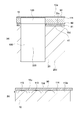
- a convex portion 113e that is in contact with the substrate 90 is formed on the outer periphery of the chuck plate 10.
- the height of the convex portion 113e is the same as the height of the convex portion 113.
- the convex portion 113e When the convex portion 113e is viewed from above in the Z-axis direction, it has an annular shape. That is, the plurality of convex portions 113 are surrounded by the convex portions 113e.
- the height of the plurality of convex portions 113 from the upper surface 10u is less than or equal to the height of the annular convex portion 113e from the upper surface 10u.
- the through hole 120 extends from the upper surface 10u to the lower surface 10d.
- the plurality of through holes 120 are arranged in a line from the center of the chuck plate 10 toward the outside of the chuck plate 10. Further, the plurality of through holes 120 are arranged, for example, at equal intervals around the center of the chuck plate 10. For example, the plurality of through holes 120 are arranged at 60° intervals with the center of the chuck plate 10 as the center.
- the chuck base 20 has an upper surface 20u (third surface) facing the lower surface 10d of the chuck plate 10 and a lower surface 20d (fourth surface) opposite to the upper surface 20u.
- the upper surface 20u and the lower surface 10d of the chuck plate 10 are joined by an adhesive layer 80.
- the planar shape of the chuck base 20 is, for example, a circle.
- the outer diameter of the chuck base 20 may be the same as the outer diameter of the chuck plate 10, or may be larger than the outer diameter of the chuck plate 10.
- the upper surface 20u of the chuck base 20 is, for example, a flat surface.
- the chuck base 20 has a through hole 220 (second through hole) penetrating from the upper surface 20u to the lower surface 20d.
- the through hole 220 communicates with the through hole 120.
- the through hole 220 also functions as a screw hole in which a screw is arranged.
- the chuck base body 20 is made of, for example, aluminum, stainless steel, or the like.
- the exhaust path 100 in the electrostatic chuck 1 is composed of a groove 110 and a through hole 120 provided in the chuck plate 10, and a through hole 220 provided in the chuck base body 20. It is not necessary for each of the plurality of through holes 220 to penetrate from the upper surface 20u of the chuck base 20 to the lower surface 20d. For example, a passage through which at least two of the plurality of through holes 220 merge and reach the lower surface 20d is formed in the chuck base 20. May be provided inside.
- the upper surface 20u of the chuck base 20 is provided with electrodes 40 and 41 arranged in the in-plane direction of the upper surface 20u.
- An insulating layer 81 is provided between the electrodes 40 and 41 and the chuck base body 20, and insulation between the electrodes 40 and 41 and the chuck base body 20 is maintained.
- a DC voltage for example, is applied between the electrode 40 and the electrode 41 by a power supply 42 provided outside.
- the chuck base 20 may be provided with a temperature adjusting mechanism for adjusting the temperature of the substrate 90.
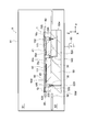
- FIG. 3 is a schematic cross-sectional view of the vacuum processing apparatus of this embodiment.
- FIG. 3 exemplifies a state in which the electrostatic chuck 1 is attached to a support in a vacuum container.
- the vacuum processing device 5 includes a vacuum container 51, an electrostatic chuck 1, a support base 50, an attachment plate 52, an exhaust mechanism 55, and a transfer mechanism 60.
- the vacuum container 51 is a vacuum container capable of maintaining a depressurized state, and accommodates the electrostatic chuck 1, the support base 50, and the deposition preventive plate 52.
- the support base 50 has an upper surface 50u (fifth surface) that supports the electrostatic chuck 1, a lower surface 50d (sixth surface) opposite to the upper surface 50u, and a side surface 50w that is continuous with the upper surface 50u and the lower surface 50d. ..
- the support table 50 may be provided with a temperature adjustment mechanism that adjusts the temperature of the substrate 90.
- the electrostatic chuck 1 is fixed to the support base 50 by the screws 30 arranged in the through holes 220 of the chuck base body 20.
- the screw 30 is a so-called vent screw.
- the screw 30 is provided with a through hole 320 that penetrates the screw 30 along the center line thereof. This through hole 320 also functions as a part of the exhaust passage 100.
- the anti-adhesion plate 52 surrounds the support base 50 inside the vacuum container 51. Due to the disposition of the deposition preventive plate 52, the inside of the vacuum container 51 is divided into a first region S1 (upper space) in which the electrostatic chuck 1 is disposed and a second region S2 (lower space) in which the support base 50 is disposed. Partitioned.
- the support base 50 is provided with a through hole 520 that penetrates from the upper surface 50u to the lower surface 50d or from the upper surface 50u to the side surface 50w and communicates with the exhaust passage 100. Since the through hole 520 is provided in the support base 50 as another exhaust path, the release gas introduced through the exhaust path 100 of the electrostatic chuck 1 is exhausted to the second region S2.
- the transfer mechanism 60 is, for example, a transfer arm, and locks the outer periphery of the substrate 90 to raise the substrate 90 from the electrostatic chuck 1 or lower it toward the electrostatic chuck 1. Further, the transfer mechanism 60 can carry out the substrate 90 raised from the electrostatic chuck 1 from the vacuum container 10 or carry the substrate 90 into the vacuum container 10. A so-called push-up pin may be used for raising and lowering the substrate 90.
- the vacuum processing apparatus 5 may be provided with a rotation mechanism that rotates the support base 50, an elevating mechanism that moves the support base 50 up and down, and the like.
- the vacuum processing apparatus 5 may be provided with an exhaust mechanism for exhausting the first region S1.
- the vacuum processing device 5 is applied to, for example, sputtering, chemical vapor deposition, ion implantation and the like.
- the vacuum processing apparatus 5 is applied to an end station of an ion implantation apparatus.
- FIG. 4 is a block diagram of the ion implanter.
- the ion implantation apparatus 1000 is an ion source 1001, a mass separator 1002, a mass separation slit 1003, an acceleration tube 1004, a quadrupole lens 1005, a scanner 1006, a collimator 1007, and an end station. And a vacuum processing device 5.
- the ion source 1001 generates ions.
- the mass separator 1002 generates a magnetic field or an electric field or both by utilizing the property that charged particles such as ions and electrons are deflected in a magnetic field or an electric field, and specifies an ion species to be injected into the substrate 90. To do.
- the acceleration tube 1004 accelerates or decelerates the desired ion species passing through the mass separation slit 1003.
- the acceleration tube 1004 applies a high voltage to a plurality of electrode pairs, and accelerates or decelerates the ions to a desired implantation energy by the action of an electrostatic field.
- the quadrupole lens 1005 adjusts the beam shape of the ions that have passed through the acceleration tube 1004.
- the scanner 1006 generates a uniform external electric field in a direction orthogonal to the traveling direction of the beam-shaped ions C that have passed through the quadrupole lens 1005, and changes the polarity and intensity of the electric field to deflect the ions. To control.
- the scanner 1006 scans the ion beam in a predetermined direction toward the input stage of the collimator 1007.
- the collimator 1007 suppresses the spread of the ion beam and forms an ion beam which is scanned in a uniaxial direction and is incident on the surface of the substrate 90.
- the collimator 1007 functions as a beam scanning unit that scans the ion beam in one axial direction.
- the substrate 90 accommodated in the vacuum processing apparatus 5 is irradiated with an ion beam.
- 5A and 5B are schematic cross-sectional views illustrating an example of the action of the electrostatic chuck.
- a wafer process is performed on the surface of the substrate 90 to form an element. Furthermore, as a part of the wafer process, the back surface of the substrate 90 may be ion-implanted. In the present embodiment, assuming that ion implantation is performed on the back surface, the substrate surface on the side supported by the chuck plate 10 is the front surface of the substrate 90, and the opposite surface is the back surface of the substrate 90.
- a protective layer 91 such as a resist is applied to the surface of the substrate 90 (FIG. 5A).
- the substrate 90 is firmly pressed against the chuck plate 10 by electrostatic attraction. Further, there is no escape path for the released gas like the exhaust path 100. Therefore, the gas generated from the protective layer 91 by the ion implantation tends to remain between the substrate 90 and the chuck plate 10.
- the release gas accumulated between the substrate 90 and the chuck plate 10 during the ion implantation leaks to the first region S1, the ion beam is exposed to the release gas. This changes the direction of the ion beam, neutralizes the ions, and reduces the energy of the ion beam.
- FIG. 5A shows the operation when the electrostatic chuck 1 of this embodiment is used.
- the substrate 90 when the back surface of the substrate 90 is ion-implanted, the substrate 90 is heated by the ion irradiation on the back surface, and gas is released from the protective layer 91.
- the electrostatic chuck 1 when the electrostatic chuck 1 is used, the space between the chuck plate 10 and the substrate 90 is sealed by the convex portion 113e provided on the outer periphery of the chuck plate 10 during electrostatic attraction. This makes it difficult for the released gas to leak from between the substrate 90 and the chuck plate 10.
- the through hole 120 communicates with the through hole 220 of the chuck base body 20.
- the released gas is efficiently exhausted from the upper surface 20u of the chuck base 20 toward the lower surface 20d.
- the flow of the released gas is simply indicated by an arrow G in FIG.
- the through hole 220 of the chuck base body 20 communicates with the through hole 520 of the support base 50, and the screw 30 is provided with the through hole 320.
- the released gas is efficiently exhausted from the upper surface 50u of the support base 50 toward the lower surface 50d through the through holes 320 and 520 (FIG. 5B).
- the substrate 90 and the lower surface 50d of the support base 50 are separated by the deposition preventive plate 52.
- the second region S2 is evacuated by the exhaust mechanism 55. Therefore, the gas released to the second area S2 is exhausted by the exhaust mechanism 55 in the second area S2. As a result, the released gas is less likely to leak to the first region S1.
- the gas is unlikely to remain between the substrate 90 and the chuck plate 10. This avoids the phenomenon that the substrate 90 jumps up from the chuck plate 10 due to the rapid volume expansion of the released gas. Moreover, since the released gas is less likely to leak into the first region S1, the direction of the ion beam is not changed, the ions are neutralized, and the energy of the ion beam is not reduced.
- the degassing process (annealing process) of the protective layer 91 becomes unnecessary. That is, the use of the electrostatic chuck 1 improves the productivity of the wafer process.
- the following processing method may be applied. Good.
- 6A to 6D are schematic sectional views showing an example of a substrate processing method.
- the electrostatic chuck 1 is prepared, and the substrate 90 is placed on the upper surface 10u thereof.
- the height of the convex portion 113 in this state is h 0 .
- the substrate 90 is electrostatically attracted to the upper surface 10u.
- the protrusions 113 and 113e are crushed, and the height of the protrusion 113 is adjusted to a height h 1 that is lower than the height h 0 .
- the electrostatic attraction force at this time is adjusted to such an extent that the substrate 90 does not come off from the chuck plate 10 even if the substrate 90 is processed.
- the substrate 90 is subjected to process processing such as ion implantation.
- the gas G is released from the protective layer 91.
- the released gas G is exhausted to the second region S2 via the exhaust passage 100 and the through hole 520.
- the height of the convex portion 113 is the height h 1 which is lower than the height h 0 , the conductance of the valley portion 114 is relatively low.
- some gas G may remain between the substrate 90 and the chuck plate 10 during process processing. If electrostatic attraction is released in this state, the substrate 90 may jump up from the chuck plate 10 due to the rapid volume expansion of the residual gas.
- the released gas G is exhausted from between the substrate 90 and the upper surface 10u of the chuck plate 10 while alleviating the electrostatic attraction without suddenly releasing the electrostatic attraction.
- the electrostatic adsorption is adjusted to be weaker than when the height is h 1 so that the height becomes h 2 (h 1 ⁇ h 2 ⁇ h 0 ). adjust.
- the height h 1 to h 2 may be changed continuously or stepwise.
- the capacitance of the valley 114 is higher than when the height is h 1 , and the conductance of the valley 114 is increased.
- the gas G generated during the process processing is reliably exhausted from between the substrate 90 and the upper surface 10u of the chuck plate 10. After that, electrostatic attraction is released, and the substrate 90 is transported by the transport mechanism 60.
- the electrostatic adsorption is relaxed continuously or stepwise to release the electrostatic adsorption until the height becomes h 0 or close to h 0. Good.
- the volume expansion due to the sudden release gas can be suppressed, and the substrate 90 can be prevented from jumping up from the chuck plate 10.
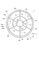
- FIG. 7 is a schematic plan view of an electrostatic chuck according to a modified example of this embodiment.
- the exhaust path 100 has a linear bank 130 provided on the upper surface 10u and a through hole 120.
- the bank portion 130 has a plurality of bank portions 131 (first bank portion) and a plurality of bank portions 132a, 132b, 132c (second bank portion).
- Each of the plurality of bank portions 131 (first bank portion) extends in a direction from the center of the chuck plate 10 to the outside of the chuck plate 10.
- the plurality of bank portions 132a, 132b, 132c intersect the plurality of bank portions 131 and are formed in an annular shape with the center of the chuck plate 10 as the center.
- the height of the plurality of bank portions 131 and the plurality of bank portions 132a, 132b, 132c from the upper surface 10u is less than or equal to the height of the convex portion 113e.
- the released gas G penetrates between the substrate 90 and the chuck plate 10 and reaches any of the through holes 120. Then, the released gas G is exhausted from between the substrate 90 and the chuck plate 10 through the through hole 120.
- Insulating layer 90 Substrate 91... Protective layer 1000... Ion implanter 1001... Ion source Reference numeral 1002... Mass separator 1003... Mass separation slit 1004... Accelerator tube 1005... Quadrupole lens 1006... Scanner 1007... Parallelizing device
Landscapes
- Chemical & Material Sciences (AREA)
- Chemical Kinetics & Catalysis (AREA)
- Engineering & Computer Science (AREA)
- Materials Engineering (AREA)
- Mechanical Engineering (AREA)
- Metallurgy (AREA)
- Organic Chemistry (AREA)
- Analytical Chemistry (AREA)
- General Chemical & Material Sciences (AREA)
- Container, Conveyance, Adherence, Positioning, Of Wafer (AREA)
- Drying Of Semiconductors (AREA)
- Physical Vapour Deposition (AREA)
Abstract
Description
1a、2a…破線
5…真空処理装置
10…チャックプレート
100…排気路
10E…領域
10d、20d、50d…下面
10u、20u、50u…上面
110…溝
111、112a、112b、112c…溝部
113、113e…凸部
114…谷部
120、220、320、520…貫通孔
130、131、132a、132b、132c…堤部
20…チャック基体
30…ネジ
40、41…電極
42…電源
50…支持台
50w…側面
51…真空容器
52…防着板
55…排気機構
60…搬送機構
80…接着剤層
81…絶縁層
90…基板
91…保護層
1000…イオン注入装置
1001…イオン源
1002…質量分離器
1003…質量分離スリット
1004…加速管
1005…四重極レンズ
1006…走査器
1007…平行化装置
Claims (8)
- 基板を支持する第1面と、前記第1面とは反対側の第2面とを有するチャックプレートを具備し、前記基板を前記第1面で支持した際に前記基板と前記第1面との間において前記基板から放出されるガスを前記基板と前記第1面との間から排気する排気路が設けられた静電チャック。
- 請求項1に記載の静電チャックであって、
前記排気路は、
前記第1面に設けられた溝と、
前記溝に連通し、前記第1面から前記第2面にまで貫通する第1貫通孔と
を有する静電チャック。 - 請求項2に記載の静電チャックであって、
前記溝は、
前記チャックプレートの中心から前記チャックプレートの外に向かう方向に延在する複数の第1溝部と、
前記複数の第1溝部に交差し、前記チャックプレートの前記中心を中心として環状に形成された複数の第2溝部と
を有する静電チャック。 - 請求項1に記載の静電チャックであって、
前記排気路は、
前記第1面に設けられた線状の堤部と、
前記第1面から前記第2面にまで貫通する第1貫通孔と
を有する静電チャック。 - 請求項1~4のいずれか1つに記載の静電チャックであって、
前記第1面に、複数の凸部と、前記複数の凸部を囲む環状の凸部とが設けられ、
前記複数の凸部の前記第1面からの高さが前記環状の凸部の高さ以下に構成されている
静電チャック。 - 請求項1~5のいずれか1つに記載の静電チャックであって、
前記チャックプレートの前記第2面に対向する第3面と、前記第3面と反対側の第4面とを有するチャック基体をさらに具備し、
前記チャック基体には、前記第3面から前記第4面にまで貫通する第2貫通孔が設けられ、前記第2貫通孔が前記第1貫通孔に連通可能に構成された
静電チャック。 - 真空容器と、
前記真空容器に収容され、基板を支持する第1面と、前記第1面とは反対側の第2面とを有するチャックプレートを具備し、前記基板を前記第1面で支持した際に前記基板と前記第1面との間において前記基板から放出されるガスを前記基板と前記第1面との間から排気する排気路が設けられた静電チャックと、
前記真空容器に収容され、前記静電チャックを支持する第5面と、前記第5面とは反対側の第6面とを有する支持台と、
前記支持台を囲み、前記静電チャックが配置される第1領域と、前記支持台が配置される第2領域とに前記真空容器の内部を区画する防着板と、
を具備し、
前記支持台には、前記排気路を通じて導かれた前記ガスを前記第2領域にまで排気する別の排気路が設けられている真空処理装置。 - 基板を支持する第1面と、前記第1面とは反対側の第2面とを有し、弾性体で構成されたチャックプレートを具備し、前記基板を前記第1面で支持した際に前記基板と前記第1面との間において前記基板から放出されるガスを前記基板と前記第1面との間から排気する排気路が前記チャックプレートに設けられた静電チャックを準備し、
凸状のエンボス加工により複数の凸部が形成された前記第1面に前記基板を載置し、
前記第1面に前記基板を静電吸着することにより、前記第1面に前記基板が載置されたときの前記複数の凸部の前記第1面からの高さh0を前記高さh0よりも低い高さh1に調整し、
前記基板にプロセス加工を施し、
前記静電吸着を緩和することにより、前記プロセス加工中に発した前記ガスを前記基板と前記第1面との間から排気する
基板処理方法。
Priority Applications (4)
| Application Number | Priority Date | Filing Date | Title |
|---|---|---|---|
| KR1020217004823A KR102515262B1 (ko) | 2018-12-05 | 2019-08-08 | 정전척, 진공처리장치 및 기판처리방법 |
| JP2020559708A JP6982701B2 (ja) | 2018-12-05 | 2019-08-08 | 静電チャック、真空処理装置及び基板処理方法 |
| US17/270,742 US12014946B2 (en) | 2018-12-05 | 2019-08-08 | Electrostatic chuck, vacuum processing apparatus, and substrate processing method |
| CN201980056824.1A CN112640082B (zh) | 2018-12-05 | 2019-08-08 | 静电吸盘、真空处理装置及基板处理方法 |
Applications Claiming Priority (2)
| Application Number | Priority Date | Filing Date | Title |
|---|---|---|---|
| JP2018-228266 | 2018-12-05 | ||
| JP2018228266 | 2018-12-05 |
Publications (1)
| Publication Number | Publication Date |
|---|---|
| WO2020115952A1 true WO2020115952A1 (ja) | 2020-06-11 |
Family
ID=70974535
Family Applications (1)
| Application Number | Title | Priority Date | Filing Date |
|---|---|---|---|
| PCT/JP2019/031443 Ceased WO2020115952A1 (ja) | 2018-12-05 | 2019-08-08 | 静電チャック、真空処理装置及び基板処理方法 |
Country Status (6)
| Country | Link |
|---|---|
| US (1) | US12014946B2 (ja) |
| JP (1) | JP6982701B2 (ja) |
| KR (1) | KR102515262B1 (ja) |
| CN (1) | CN112640082B (ja) |
| TW (1) | TWI750502B (ja) |
| WO (1) | WO2020115952A1 (ja) |
Cited By (2)
| Publication number | Priority date | Publication date | Assignee | Title |
|---|---|---|---|---|
| KR20240109926A (ko) | 2023-01-05 | 2024-07-12 | 도쿄엘렉트론가부시키가이샤 | 정전 척, 기판 처리 장치, 및 정전 척의 제조 방법 |
| KR20240109919A (ko) | 2023-01-05 | 2024-07-12 | 도쿄엘렉트론가부시키가이샤 | 정전 척, 기판 처리 장치, 및 정전 척의 제조 방법 |
Families Citing this family (1)
| Publication number | Priority date | Publication date | Assignee | Title |
|---|---|---|---|---|
| CN115132635A (zh) * | 2021-03-24 | 2022-09-30 | Toto株式会社 | 静电吸盘以及半导体制造装置 |
Citations (2)
| Publication number | Priority date | Publication date | Assignee | Title |
|---|---|---|---|---|
| JP2003282690A (ja) * | 2002-03-25 | 2003-10-03 | Toto Ltd | 静電チャック |
| JP2012216774A (ja) * | 2011-04-01 | 2012-11-08 | Hitachi Kokusai Electric Inc | 基板処理装置、半導体装置の製造方法、基板処理方法及びサセプタカバー |
Family Cites Families (11)
| Publication number | Priority date | Publication date | Assignee | Title |
|---|---|---|---|---|
| JPH06244269A (ja) * | 1992-09-07 | 1994-09-02 | Mitsubishi Electric Corp | 半導体製造装置並びに半導体製造装置におけるウエハ真空チャック装置及びガスクリーニング方法及び窒化膜形成方法 |
| JP3636864B2 (ja) * | 1997-06-11 | 2005-04-06 | 東京エレクトロン株式会社 | 処理装置およびステージ装置 |
| WO2006001425A1 (ja) * | 2004-06-28 | 2006-01-05 | Kyocera Corporation | 静電チャック |
| US20060037702A1 (en) * | 2004-08-20 | 2006-02-23 | Tokyo Electron Limited | Plasma processing apparatus |
| KR100711729B1 (ko) * | 2005-10-25 | 2007-04-25 | 세메스 주식회사 | 냉각 플레이트 및 베이크 장치 |
| JP5035884B2 (ja) * | 2007-03-27 | 2012-09-26 | 東京エレクトロン株式会社 | 熱伝導シート及びこれを用いた被処理基板の載置装置 |
| US8540819B2 (en) * | 2008-03-21 | 2013-09-24 | Ngk Insulators, Ltd. | Ceramic heater |
| JP6010433B2 (ja) * | 2012-11-15 | 2016-10-19 | 東京エレクトロン株式会社 | 基板載置台および基板処理装置 |
| CN105408992B (zh) * | 2013-08-05 | 2019-01-29 | 应用材料公司 | 用于薄基板搬运的静电载体 |
| JP5987966B2 (ja) | 2014-12-10 | 2016-09-07 | Toto株式会社 | 静電チャックおよびウェーハ処理装置 |
| JP2018085408A (ja) * | 2016-11-22 | 2018-05-31 | 株式会社ディスコ | 減圧処理装置 |
-
2019
- 2019-08-08 KR KR1020217004823A patent/KR102515262B1/ko active Active
- 2019-08-08 WO PCT/JP2019/031443 patent/WO2020115952A1/ja not_active Ceased
- 2019-08-08 US US17/270,742 patent/US12014946B2/en active Active
- 2019-08-08 CN CN201980056824.1A patent/CN112640082B/zh active Active
- 2019-08-08 JP JP2020559708A patent/JP6982701B2/ja active Active
- 2019-08-28 TW TW108130813A patent/TWI750502B/zh active
Patent Citations (2)
| Publication number | Priority date | Publication date | Assignee | Title |
|---|---|---|---|---|
| JP2003282690A (ja) * | 2002-03-25 | 2003-10-03 | Toto Ltd | 静電チャック |
| JP2012216774A (ja) * | 2011-04-01 | 2012-11-08 | Hitachi Kokusai Electric Inc | 基板処理装置、半導体装置の製造方法、基板処理方法及びサセプタカバー |
Cited By (2)
| Publication number | Priority date | Publication date | Assignee | Title |
|---|---|---|---|---|
| KR20240109926A (ko) | 2023-01-05 | 2024-07-12 | 도쿄엘렉트론가부시키가이샤 | 정전 척, 기판 처리 장치, 및 정전 척의 제조 방법 |
| KR20240109919A (ko) | 2023-01-05 | 2024-07-12 | 도쿄엘렉트론가부시키가이샤 | 정전 척, 기판 처리 장치, 및 정전 척의 제조 방법 |
Also Published As
| Publication number | Publication date |
|---|---|
| KR102515262B1 (ko) | 2023-03-29 |
| CN112640082B (zh) | 2023-12-26 |
| US12014946B2 (en) | 2024-06-18 |
| JP6982701B2 (ja) | 2021-12-17 |
| TW202022980A (zh) | 2020-06-16 |
| US20210296154A1 (en) | 2021-09-23 |
| JPWO2020115952A1 (ja) | 2021-09-02 |
| KR20210032487A (ko) | 2021-03-24 |
| CN112640082A (zh) | 2021-04-09 |
| TWI750502B (zh) | 2021-12-21 |
Similar Documents
| Publication | Publication Date | Title |
|---|---|---|
| JP4676074B2 (ja) | フォーカスリング及びプラズマ処理装置 | |
| US9349618B2 (en) | Substrate processing apparatus | |
| JP5250408B2 (ja) | 基板温調固定装置 | |
| JP6982701B2 (ja) | 静電チャック、真空処理装置及び基板処理方法 | |
| KR20100085920A (ko) | 이온 주입에 의해 활성화되는 웨이퍼 본딩 | |
| US20100214712A1 (en) | Method for charge-neutralizing target substrate and substrate processing apparatus | |
| US8681472B2 (en) | Platen ground pin for connecting substrate to ground | |
| JP2012524417A (ja) | 基板と静電クランプとの間の電荷の除去 | |
| KR20150085793A (ko) | 기판 처리 장치 | |
| WO2016167233A1 (ja) | 基板保持機構、成膜装置、および基板の保持方法 | |
| KR100599037B1 (ko) | 이온 소스 및 이를 갖는 이온 주입 장치 | |
| JP2008028360A (ja) | プラズマを用いたイオン注入装置 | |
| US10692686B2 (en) | Surface treatment apparatus using plasma | |
| US8197638B2 (en) | Semiconductor manufacturing device and method for manufacturing semiconductor devices | |
| US7858155B2 (en) | Plasma processing method and plasma processing apparatus | |
| KR101517720B1 (ko) | 정전척 및 이를 포함하는 플라즈마 발생장치 | |
| KR20250175798A (ko) | 플라즈마 식각 장치용 밀폐 링 어셈블리 및 이를 포함하는 플라즈마 식각 장치 | |
| JP5898433B2 (ja) | イオンドーピング装置及び半導体装置の作製方法 | |
| JP2005045124A (ja) | ステンシルマスク、荷電粒子照射装置及び方法 | |
| US20180233386A1 (en) | Platen For Reducing Particle Contamination On A Substrate and a Method Thereof | |
| CN109068467A (zh) | 一种除静电装置及除静电方法 | |
| CN1706026A (zh) | 具有边缘遮蔽和气体清除的静电卡盘晶片端口和顶板 | |
| JP7763531B1 (ja) | プラズマコンファイニングのためのバッフルを含むプラズマ処理装置 | |
| JP7122551B2 (ja) | プラズマ処理装置 | |
| KR102521976B1 (ko) | 기판 도핑 방법 |
Legal Events
| Date | Code | Title | Description |
|---|---|---|---|
| 121 | Ep: the epo has been informed by wipo that ep was designated in this application |
Ref document number: 19893456 Country of ref document: EP Kind code of ref document: A1 |
|
| ENP | Entry into the national phase |
Ref document number: 2020559708 Country of ref document: JP Kind code of ref document: A |
|
| ENP | Entry into the national phase |
Ref document number: 20217004823 Country of ref document: KR Kind code of ref document: A |
|
| NENP | Non-entry into the national phase |
Ref country code: DE |
|
| 122 | Ep: pct application non-entry in european phase |
Ref document number: 19893456 Country of ref document: EP Kind code of ref document: A1 |