WO2020115871A1 - GaAs基板の製造方法およびGaAs単結晶成長装置 - Google Patents
GaAs基板の製造方法およびGaAs単結晶成長装置 Download PDFInfo
- Publication number
- WO2020115871A1 WO2020115871A1 PCT/JP2018/044954 JP2018044954W WO2020115871A1 WO 2020115871 A1 WO2020115871 A1 WO 2020115871A1 JP 2018044954 W JP2018044954 W JP 2018044954W WO 2020115871 A1 WO2020115871 A1 WO 2020115871A1
- Authority
- WO
- WIPO (PCT)
- Prior art keywords
- gaas
- single crystal
- crucible
- gaas single
- melt
- Prior art date
- Legal status (The legal status is an assumption and is not a legal conclusion. Google has not performed a legal analysis and makes no representation as to the accuracy of the status listed.)
- Ceased
Links
- 0 C[C@@]1(CC(CCC2)CC2C[C@]2(C)ICC3CC(CCCC(CC*C4)C[C@@]4(C*)SC*)CCC3)IC2(IIC)IC[C@](CCC2)CC2C1 Chemical compound C[C@@]1(CC(CCC2)CC2C[C@]2(C)ICC3CC(CCCC(CC*C4)C[C@@]4(C*)SC*)CCC3)IC2(IIC)IC[C@](CCC2)CC2C1 0.000 description 1
Images


Classifications
-
- C—CHEMISTRY; METALLURGY
- C30—CRYSTAL GROWTH
- C30B—SINGLE-CRYSTAL GROWTH; UNIDIRECTIONAL SOLIDIFICATION OF EUTECTIC MATERIAL OR UNIDIRECTIONAL DEMIXING OF EUTECTOID MATERIAL; REFINING BY ZONE-MELTING OF MATERIAL; PRODUCTION OF A HOMOGENEOUS POLYCRYSTALLINE MATERIAL WITH DEFINED STRUCTURE; SINGLE CRYSTALS OR HOMOGENEOUS POLYCRYSTALLINE MATERIAL WITH DEFINED STRUCTURE; AFTER-TREATMENT OF SINGLE CRYSTALS OR A HOMOGENEOUS POLYCRYSTALLINE MATERIAL WITH DEFINED STRUCTURE; APPARATUS THEREFOR
- C30B11/00—Single-crystal growth by normal freezing or freezing under temperature gradient, e.g. Bridgman-Stockbarger method
-
- C—CHEMISTRY; METALLURGY
- C30—CRYSTAL GROWTH
- C30B—SINGLE-CRYSTAL GROWTH; UNIDIRECTIONAL SOLIDIFICATION OF EUTECTIC MATERIAL OR UNIDIRECTIONAL DEMIXING OF EUTECTOID MATERIAL; REFINING BY ZONE-MELTING OF MATERIAL; PRODUCTION OF A HOMOGENEOUS POLYCRYSTALLINE MATERIAL WITH DEFINED STRUCTURE; SINGLE CRYSTALS OR HOMOGENEOUS POLYCRYSTALLINE MATERIAL WITH DEFINED STRUCTURE; AFTER-TREATMENT OF SINGLE CRYSTALS OR A HOMOGENEOUS POLYCRYSTALLINE MATERIAL WITH DEFINED STRUCTURE; APPARATUS THEREFOR
- C30B29/00—Single crystals or homogeneous polycrystalline material with defined structure characterised by the material or by their shape
- C30B29/10—Inorganic compounds or compositions
- C30B29/40—AIIIBV compounds wherein A is B, Al, Ga, In or Tl and B is N, P, As, Sb or Bi
- C30B29/42—Gallium arsenide
Definitions
- the present disclosure relates to a GaAs substrate manufacturing method and a GaAs single crystal growth apparatus.
- Patent Document 1 discloses a pulling method (LEC method), a horizontal Bridgman method, a vertical Bridgman method, etc. as a method for obtaining a GaAs single crystal and a GaAs substrate using the same. Various methods are disclosed.
- a method of manufacturing a GaAs substrate according to the present disclosure is a method of manufacturing a GaAs substrate whose main surface has a plane orientation of (100), and includes a first crucible in which GaAs is housed and a lower portion than the first crucible.
- a GaAs single crystal growth apparatus includes a first crucible in which GaAs is housed, and a second crucible arranged below the first crucible and in which a GaAs seed crystal is housed in the bottom. Is a melt by being heated in the first crucible, the melt is dropped into the second crucible, and the GaAs seed crystal and the melt on the GaAs seed crystal are temperature-controlled. To grow a GaAs single crystal from the above GaAs seed crystal.
- FIG. 1A is an example of a GaAs single crystal growth apparatus used in the method of manufacturing a GaAs substrate according to the present disclosure, and is a schematic view of a GaAs single crystal growth apparatus in a state before the first GaAs raw material is heated in the first crucible. It is sectional drawing which shows a structure.
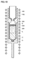
- FIG. 1B is an example of a GaAs single crystal growth apparatus used in the method of manufacturing a GaAs substrate according to the present disclosure, and particularly shows a schematic configuration of the GaAs single crystal growth apparatus in the state of growing a GaAs single crystal from a GaAs seed crystal. It is sectional drawing shown.
- FIG. 2 is a horizontal sectional view illustrating an example of a schematic configuration of the second support member in FIGS. 1A and 1B.
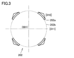
- FIG. 3 is a horizontal cross-sectional view illustrating another example of the schematic configuration of the second support member in FIGS. 1A and 1B.
- the processing loss as described above is reduced, but since it is not the direct synthesis method, the loss at the stage of preparing the raw material (hereinafter, “ Also referred to as "raw material loss”). That is, solid GaAs is synthesized in a predetermined synthesis furnace, and this is divided and transferred to a single crystal growth crucible in a heating furnace different from the above synthesis furnace. Occurs. Therefore, a technique for obtaining a GaAs single crystal in which the raw material loss is sufficiently reduced and a GaAs substrate containing the same has not been realized yet, and the development thereof is earnestly desired.
- the present disclosure aims to provide a GaAs substrate manufacturing method and a GaAs single crystal growth apparatus capable of obtaining a GaAs substrate in which the raw material loss is sufficiently reduced.
- a GaAs single crystal is grown using a vertical cylindrical in-container crystal growth method common to the vertical Bridgman method and the vertical temperature gradient solidification method, a so-called vertical boat method (hereinafter, also referred to as “VB method”).
- VB method vertical boat method
- the GaAs synthesizing crucible was positioned above the GaAs single crystal growth crucible with the synthesized solid GaAs being housed therein, and the solid GaAs was heated to form a melt.
- the present invention has been conceived and arrived at the present disclosure by conceiving a method of growing a GaAs single crystal by sufficiently reducing the raw material loss by dropping into the crucible for growing a single crystal as in the direct synthesis method.
- a method of manufacturing a GaAs substrate according to an aspect of the present disclosure is a method of manufacturing a GaAs substrate in which a main surface has a (100) plane orientation, and a first crucible containing GaAs and the above-mentioned first crucible.
- the GaAs single crystal growth apparatus further includes a support member that is disposed along the outer periphery of the second crucible and that supports the first crucible. This makes it possible to easily support the load of the first crucible and GaAs in the first crucible.
- the support member has a cylindrical shape having a side surface having a plurality of support columns and openings formed between the plurality of support sections, and the opening is formed by the growing GaAs single crystal.
- the crystal is preferably formed in the [011] direction and a direction equivalent to the [011] direction.
- the thermal stress can be made approximately the same between the [010] direction and the [011] direction, so that the dislocation density on the main surface is uniform.
- GaAs substrate can be obtained.
- the supporting member has a cylindrical shape having a side surface having a plurality of supporting columns and an opening formed between the plurality of supporting columns, and the supporting column is formed by the growing GaAs monolayer.
- the crystal is preferably formed in the [010] direction and a direction equivalent to the [010] direction. This makes it possible to reduce the temperature difference between the central part and the outer peripheral part in the [010] direction and the direction equivalent to the [010] direction of the growing GaAs single crystal, and thus the dislocation density on the main surface can be reduced. It is possible to obtain a uniform GaAs substrate.
- the dislocation density of the GaAs substrate is generally evaluated in two directions of the [010] direction and the [011] direction in the GaAs substrate when the principal plane of the GaAs substrate is the (100) plane.
- the dislocation density is likely to be maximized in the outer peripheral portion in the [010] direction, and the dislocation density is likely to be minimum near the radial midpoint in the [011] direction. This is because it will be characteristic in doing so.
- a GaAs single crystal is conventionally grown by providing a constant temperature difference between the central portion and the outer peripheral portion of the GaAs single crystal during crystal growth.
- the shape of the surface (the interface between the GaAs single crystal and the melt) is made to be a paraboloid that is convex in the growth direction.
- the above temperature difference appears as thermal stress in the growing GaAs single crystal. Due to the characteristics of the GaAs single crystal C, when the growth direction of the GaAs single crystal is the [100] direction, the thermal stress tends to appear larger in the [010] direction of the GaAs single crystal C than in the [011] direction.
- the pillar portion so as to block the [010] direction of the growing GaAs single crystal and the direction equivalent to the [010] direction.
- the temperature of the portion of the crucible located behind the column is lower than the temperature of the other portion of the crucible, and the temperature difference is at least equivalent to the [010] direction and the [010] direction of the single crystal.
- the crucible can be formed.
- the thermal stress can be made approximately the same between the [010] direction and the [011] direction. Therefore, according to the present disclosure, a GaAs substrate having a uniform dislocation density in the [010] direction and the [011] direction can be obtained.
- the column section has a horizontal cross section that is convex in the radial direction of the cylindrical shape.
- the supporting member preferably contains any one selected from the group consisting of mullite, carbon, quartz, alumina and silicon carbide. This makes it possible to easily reduce the temperature difference in the [010] direction of the GaAs single crystal and in a direction equivalent to the [010] direction, thereby easily obtaining a GaAs substrate having a uniform dislocation density on the main surface. be able to.
- a GaAs single crystal growth apparatus includes a first crucible in which GaAs is housed, and a second crucible that is arranged below the first crucible and in which a GaAs seed crystal is housed in the bottom. And the GaAs becomes a melt by being heated in the first crucible, and the melt is dripped into the second crucible and melts on the GaAs seed crystal and the GaAs seed crystal. The liquid is heated to grow a GaAs single crystal from the GaAs seed crystal.
- the GaAs single crystal growth apparatus having such characteristics can sufficiently reduce the raw material loss for obtaining the GaAs single crystal.
- the GaAs single crystal growth apparatus further includes a support member that is arranged along the outer periphery of the second crucible and supports the first crucible. This makes it possible to easily support the load of the first crucible and GaAs in the first crucible.
- the supporting member has a cylindrical shape having a side surface having a plurality of supporting columns and openings formed between the plurality of supporting columns, and the opening is formed by the growing GaAs monolayer.
- the crystal is preferably formed in the [011] direction and a direction equivalent to the [011] direction.
- the supporting member has a cylindrical shape having a side surface having a plurality of supporting columns and an opening formed between the plurality of supporting columns, and the supporting column is formed by the growing GaAs monolayer.
- the crystal is preferably formed in the [010] direction and a direction equivalent to the [010] direction. This makes it possible to reduce the temperature difference between the central part and the outer peripheral part in the [010] direction and the direction equivalent to the [010] direction of the growing GaAs single crystal, and thus the dislocation density on the main surface can be reduced.
- a uniform GaAs substrate can be manufactured.
- the column portion has a shape in which the horizontal cross section is convex in the radial direction of the cylindrical shape.
- the support member preferably contains any one selected from the group consisting of mullite, carbon, quartz, alumina and silicon carbide. This makes it possible to easily reduce the temperature difference in the [010] direction of the GaAs single crystal and in a direction equivalent to the [010] direction, thereby easily manufacturing a GaAs substrate having a uniform dislocation density on the main surface. can do.
- the notation of the form “AB” means the upper and lower limits of the range (that is, A or more and B or less), and when A does not have a unit and B only has a unit, A The unit of B and the unit of B are the same.
- the method for manufacturing a GaAs substrate according to this embodiment is a method for manufacturing a GaAs substrate in which the plane orientation of the main surface is the (100) plane.
- a GaAs substrate is manufactured by arranging a first crucible 101 containing GaAs and a first crucible 101 below the first crucible 101.
- the GaAs seed crystal S is converted into the GaAs single crystal C.
- the step of growing (second step) and the step of cutting the GaAs single crystal C perpendicular to the growth direction thereof to obtain a GaAs substrate having the main surface with the (100) plane orientation (third step). Process) and.
- the GaAs single crystal growth apparatus further includes a support member that is provided along the outer periphery of the second crucible 201 and supports the first crucible 101.
- the "growth direction" of a GaAs single crystal means a direction in which a GaAs seed crystal grows into a GaAs single crystal from a melt of GaAs as a starting material, and is usually referred to as a GaAs single crystal.
- the GaAs substrate obtained by the above-described manufacturing method has the main surface having the (100) plane orientation.
- the first step is a GaAs single crystal growth apparatus provided with a first crucible 101 containing GaAs and a second crucible 201 arranged below the first crucible 101 and containing a GaAs seed crystal S at the bottom. Is a step of preparing. That is, the first step is a step of preparing a GaAs single crystal growth apparatus as illustrated in FIGS. 1A and 1B.
- the GaAs single crystal growth apparatus shown in FIGS. 1A and 1B includes a first crucible 101 in which a first GaAs raw material S2 as solid GaAs, which is a raw material, is housed, and is arranged below the first crucible 101.
- the second crucible 201 in which S is housed in the bottom is provided.
- the GaAs single crystal growth apparatus further includes a support member that is disposed along the outer periphery of the second crucible 201 and supports the first crucible 101.
- the GaAs single crystal growth apparatus can include a heating element 301 arranged along the outer periphery of the support member.
- the supporting member faces the first crucible 101 in FIGS. 1A and 1B, thereby supporting the first crucible 101 via an intervening member that supports the first crucible 101.
- the intervening member as the first supporting member 102 and the supporting member as the second supporting member 202.
- a first GaAs raw material S2 which is a raw material of a melt L formed by heating GaAs in a second step described later, is shown in the first crucible 101, and a GaAs seed crystal is provided in the second crucible 201.
- FIG. 1B the GaAs single crystal C and the GaAs seed crystal S are shown as having separate interfaces for convenience of description, but the GaAs single crystal C is the GaAs seed crystal S. Since they grow in the same crystal direction as the starting point, there is no interface between them.
- the second GaAs raw material S3 when the melt L directly contacts the GaAs seed crystal S in the second step described later, there is a possibility that dislocations may enter the GaAs seed crystal S due to thermal shock caused by the high temperature melt L. Since it becomes high, it is preferable to place it in advance on the GaAs seed crystal S for the purpose of preventing this.
- the second GaAs raw material S3 can be stored in the second crucible 201 by a known method.
- the first crucible 101 has a cylindrical shape in which the bottom is tapered and contracted toward the lower end, and the first GaAs raw material S2 is housed inside. This first GaAs raw material S2 is preferably solid.
- the first crucible 101 preferably has an opening at the lower end of the bottom.
- the first GaAs raw material S2 can be manufactured by a conventionally known method. For example, first, liquid Ga and solid As are prepared in predetermined synthesis furnaces in an amount of 1:1 in molar ratio. Next, As is heated to 660° C. or higher to be sublimated into gas. It can be obtained by sending As into a gas into a liquid of Ga by an injection method, reacting Ga with As, and then solidifying this. As the first crucible 101, it is preferable to use the crucible in the synthesis furnace as it is.
- the first crucible 101 can be made of any conventionally known material as long as it is a material that can withstand heat at 1238° C. and can withstand thermal shock. Examples of the material of the first crucible 101 include carbon, boron nitride (BN), and quartz.
- the opening at the bottom of the first crucible 101 is preferably provided with a mechanism that can be automatically or manually opened and closed.
- the first support member 102 supports the first crucible 101 by facing the first crucible 101. Specifically, the first support member 102 faces the first crucible 101 from below and supports the first crucible 101 so as to surround the first crucible 101.
- the first support member 102 may have any shape as long as the first support member 102 can support the first crucible 101 and the effect of the present disclosure can be obtained. However, it is preferable that the first supporting member 102 has a through hole portion through which the melt L dropped from the opening at the bottom of the first crucible 101 passes, at a position corresponding to the opening at the bottom of the first crucible 101.
- any conventionally known material can be used as long as the effects of the present disclosure are exhibited.
- the material of the first supporting member 102 include mullite, carbon, quartz, alumina, silicon carbide, silicon nitride and the like.
- a CVD carbon coating, a SiC coating, or a glassy carbon coating may be applied as a measure against dust generation.
- the second crucible 201 is arranged below the first crucible 101. Further, the second crucible 201 is arranged below the first support member 102.
- the second crucible 201 has a cylindrical shape in which the bottom portion is tapered and contracted toward the lower end, and the GaAs seed crystal S is accommodated in the bottom portion.
- the GaAs seed crystal S has a (100) plane that is perpendicular to the growth direction of the GaAs single crystal C.
- the GaAs seed crystal S a GaAs single crystal manufactured by a conventionally known method can be used.
- the GaAs seed crystal S is manufactured based on the VB method, the liquid sealed Czochralski method (pulling method, LEC method), the vapor pressure controlled Czochralski method (VCZ method), the horizontal Bridgman method (HB method), and the like. can do.
- Impurities such as carbon, boron, and oxygen can be doped (added) into the GaAs seed crystal S as dopants.
- the inner diameter of the second crucible 201 corresponds to the diameter of the growing GaAs single crystal C, that is, the diameter of the GaAs substrate. Therefore, the inner diameter of the second crucible 201 is preferably 150 to 200 mm.
- the material of the second crucible 201 a known material can be used as in the case of the first crucible 101. Examples of the material of the second crucible 201 include carbon, boron nitride (BN), silicon nitride (Si 3 N 4 ), alumina (Al 2 O 3 ), silicon carbide (SiC) and the like.
- the second support member 202 is arranged along the outer circumference of the second crucible 201.
- the second support member 202 preferably supports the first crucible 101 via the first support member 102.
- the GaAs single crystal growth apparatus can easily support the load of the first crucible 101 and the first GaAs raw material S2 in the first crucible 101 by the second support member 202.
- the second support member 202 preferably has a cylindrical shape having a side surface having a plurality of support columns 202a and a plurality of openings 202b.
- the pillar 202a is preferably formed so as to block the [010] direction of the growing GaAs single crystal C and the direction equivalent to this [010] direction.
- each of the plurality of openings 202b is formed between the adjacent pillars 202a so as to be located in the [011] direction of the growing GaAs single crystal C and in a direction equivalent to this [011] direction.
- the horizontal cross section of the pillar 202a has an arc shape that forms a part of the cylindrical shape.
- the GaAs single crystal growth apparatus can make the thermal stresses in the [010] direction and the [011] direction of the GaAs single crystal C during growth almost the same, and thus the dislocation density on the main surface can be increased. It is possible to obtain a GaAs substrate in which
- a constant temperature difference is provided between the central portion and the outer peripheral portion of the GaAs single crystal during crystal growth as described above, so that the growth surface of the GaAs single crystal (interface between the GaAs single crystal and the melt) is The shape is a paraboloid that is convex in the growth direction. Due to this temperature difference, thermal stress is generated in the growing GaAs single crystal. Due to the characteristics of the GaAs single crystal C, when the growth direction of the GaAs single crystal is the [100] direction, the thermal stress tends to appear larger in the [010] direction of the GaAs single crystal C than in the [011] direction.
- the pillar portion 202a is formed so as to block the [010] direction of the growing GaAs single crystal C and the direction equivalent to the [010] direction.
- the opening 202b is formed between the adjacent pillars 202a so that the opening 202b is located in the [011] direction of the growing GaAs single crystal C and in the direction equivalent to the [011] direction.
- the temperature of the portion of the second crucible 201 located behind the support column 202a can be lower than the temperature of the portion of the second crucible 201 located behind the opening 202b. This makes it possible to reduce the temperature difference in the [010] direction of the GaAs single crystal C and in the direction equivalent to the [010] direction.
- the pillar portion 202a made of carbon and having a thickness of 5 mm is arranged so as to block the [010] direction and the direction equivalent to the [010] direction of the GaAs single crystal C having a diameter of 150 mm to be grown
- the GaAs A general temperature difference (about 5° C.) provided between the central portion and the outer peripheral portion of the single crystal C can be reduced by about 1° C.
- the thermal stress can be made approximately the same between the [010] direction and the [011] direction of the GaAs single crystal C.
- the column portion 202a has a shape in which the horizontal cross section thereof has a cylindrical shape that is convex in the radial direction. Specifically, in the arc shape that appears as a horizontal cross section of the pillar portion 202a, the outer side of the arc shape is projected.
- the temperature of the portion where the large thermal stress is generated can be effectively reduced, and thus the above temperature difference. Can be reduced only in the [010] direction and the direction equivalent to the [010] direction of the GaAs single crystal C.
- the material used for the second support member 202 should not be particularly limited as long as the effects of the present disclosure are exhibited.
- the second supporting member 202 is made of any one selected from the group consisting of mullite, carbon, quartz, alumina and silicon carbide from the viewpoint of reducing the temperature difference between the central portion and the outer peripheral portion of the growing GaAs single crystal C. It is preferable to include. Further, the second support member 202 is more preferably made of any one selected from the group consisting of mullite, carbon, quartz, alumina and silicon carbide.
- the directions equivalent to the [011] direction of the GaAs single crystal C are the [011] direction, the [01-1] direction, the [0-1-1] direction, and the [0-11] direction. Means four directions.
- the direction equivalent to the [010] direction of the GaAs single crystal C means four directions of [010] direction, [00-1] direction, [0-10] direction and [001] direction.
- the "-" that is shown when describing the crystal orientation is originally shown above the number and is read as "bar".
- [01-1] is read as "zero-ichi-bar".
- the GaAs single crystal growth apparatus shown in FIGS. 1A and 1B can include the heating element 301 as described above.
- the heating element 301 is arranged along the outer circumference of the second support member 202.
- the heating element 301 is a linear heating element, and is arranged so as to spirally surround the outer peripheral surface of the second support member 202 along the growth direction of the GaAs single crystal C.
- a circle that appears when the spiral shape is viewed from above from the top a circle that appears when the second crucible 201 is viewed from above and the second support member 202 is viewed from above when viewed from above. Concentric circles are preferred in relation to the appearing circle.
- the second crucible 201 and the heating element 301 have a relationship in which the shortest distance from the outer peripheral surface of the second crucible 201 to the heating element 301 is a concentric circle of 4 to 12 cm. It is preferable that the second support member 202 and the heating element 301 have a relationship in which the shortest distance from the outer peripheral surface of the second support member 202 to the heating element 301 is a concentric circle of 2 to 10 cm.
- the heating element 301 can be made of any conventionally known material as long as the effects of the present disclosure are exhibited. Above all, since the heating element 301 has a high temperature of 1000° C. or higher, a heat-resistant material such as Fe—Cr—Al-based heating element, MoSi 2 -based heating element, carbon, or molybdenum can be preferably used.
- the GaAs single crystal growth apparatus as described above is prepared.
- the solid first GaAs raw material S2 synthesized in a predetermined synthesis furnace can be used for growing a GaAs single crystal without dividing it. That is, in the first step, the GaAs synthesizing crucible can be positioned above the second crucible 201 by using it as the first crucible 101 of the GaAs single crystal growth apparatus in a state of containing the first GaAs raw material S2 synthesized. it can. Then, as described later, the first GaAs raw material S2 becomes a melt L by being heated in the first crucible 101.
- This melt L is dripped into the second crucible 201, and after this is completed, the GaAs seed crystal S, the second GaAs raw material S3 on the GaAs seed crystal S, and the melt L are subjected to temperature control so that the GaAs seed crystal A GaAs single crystal C is grown from S. Therefore, it is not necessary to divide the solid GaAs (first GaAs raw material S2) synthesized in a predetermined synthesis furnace and then transfer it to a single crystal growth crucible different from the above synthesis furnace, and the raw material loss can be reduced.
- ⁇ Second step> the first GaAs raw material S2 in the first crucible 101 was heated in the GaAs single crystal growth apparatus to form a melt L, and the melt L was dropped into the second crucible 201 to complete this. After that, by controlling the temperature of the GaAs seed crystal S and the melt L on the GaAs seed crystal S, a GaAs single crystal C is grown from the GaAs seed crystal S. Particularly, in the second step, when the melt L directly contacts the GaAs seed crystal S, there is a high possibility that dislocations will enter the GaAs seed crystal S due to thermal shock caused by the high-temperature melt L, and this is prevented.
- the second GaAs raw material S3 is placed on the GaAs seed crystal S in advance. Therefore, in the second step, the temperature of the GaAs seed crystal S, the second GaAs raw material S3 on the GaAs seed crystal S, and the melt L are controlled by the heat from the heating element 301. At this time, the second GaAs raw material S3 also becomes the melt L by the heat from the heating element 301.
- the GaAs single crystal C is composed of a melt L derived from the second GaAs raw material S3 on the GaAs seed crystal S and a melt derived from the first GaAs raw material S2, starting from the GaAs seed crystal S.
- the growth surface of the growing GaAs single crystal C is preferably a paraboloid whose shape is convex in the growth direction of the GaAs single crystal C.
- control the temperature of the GaAs seed crystal S and the melt L on the GaAs seed crystal S means that the GaAs seed crystal S is heated to melt a part of the GaAs seed crystal S or the melt L is melted. Is an operation of raising or lowering the temperature of heat generated from a heating element, such as an operation of temporarily suspending heating to cool the GaAs single crystal C to cool the material. This "controlling the temperature” also includes the operation of heating the second GaAs raw material S3 in order to melt it.
- the above-described second support member 202 is prepared in the first step.
- the second support member 202 has a cylindrical shape with a side surface having a plurality of support columns 202a and an opening 202b formed between the plurality of support columns 202a, and is arranged along the outer periphery of the second crucible 201. Is set up.
- the pillar portion 202a is formed in the [010] direction of the growing GaAs single crystal C and in a direction equivalent to this [010] direction.
- the opening 202b is formed in the [011] direction of the growing GaAs single crystal C and in a direction equivalent to this [011] direction.
- the thermal stress is made approximately the same between the [010] direction and the [011] direction. be able to. Specifically, at the interface between the growing GaAs single crystal C and the melt L, the variation in thermal stress between the [010] direction and the [011] direction can be set to 20% or less.
- the third step is a step of cutting the GaAs single crystal C perpendicularly to the growth direction thereof to obtain a GaAs substrate having a main surface whose plane orientation is the (100) plane.
- the GaAs single crystal C can be cut out perpendicularly to its growth direction by using a conventionally known method.
- a GaAs substrate can be obtained by performing mirror processing or the like if necessary.
- the plane orientation perpendicular to the growth direction of the GaAs single crystal C is set to the (100) plane.
- the GaAs seed crystal S is housed in the bottom of the two crucible 201.
- the GaAs single crystal C grown in the second step is cut out perpendicularly to its growth direction (that is, the [100] direction) to obtain a GaAs substrate whose principal plane is the (100) plane. Can be easily obtained.
- the method for manufacturing a GaAs substrate according to the present embodiment can grow a GaAs single crystal C without dividing solid GaAs synthesized in a predetermined synthesis furnace. Therefore, a GaAs substrate in which the raw material loss is sufficiently reduced can be obtained. Further, in the GaAs substrate obtained by the above-described manufacturing method, when the dislocation density is measured on the main surface thereof, variations in the dislocation density are suppressed in any crystal orientation, so that the dislocation density becomes uniform in any crystal orientation. Therefore, the GaAs substrate manufacturing method according to the present embodiment can obtain a GaAs substrate having a uniform dislocation density in all crystal orientations of the main surface.
- the GaAs substrate obtained by the above-described manufacturing method has the main surface having the (100) plane orientation. Furthermore, the GaAs substrate obtained by the above manufacturing method is preferably semi-insulating.
- the “semi-insulating property” refers to the property of exhibiting a high specific resistance of 1 M ⁇ cm or more and 1000 M ⁇ cm or less.
- the GaAs substrate obtained by the above manufacturing method can have a disc shape with a diameter of 150 mm or more.
- the GaAs substrate manufacturing method according to the present embodiment can obtain a GaAs substrate in which the raw material loss is sufficiently reduced even if the diameter is generally 150 mm or more.
- the upper limit of the diameter of the GaAs substrate is 200 mm due to restrictions on manufacturing equipment.
- a GaAs substrate having a diameter of 150 mm includes a 6-inch GaAs substrate.
- the GaAs substrate with a diameter of 200 mm includes an 8-inch GaAs substrate.
- the GaAs substrate obtained by the above-mentioned manufacturing method, when the dislocation density is measured on the main surface of the GaAs substrate, the dislocation density is uniform in any crystal orientation, so that the dislocation density is uniform in any crystal orientation. Therefore, the GaAs substrate can be suitably used for an optical device or an electronic device that performs transmission/reception, signal processing, etc. in the technical fields of wireless communication, optical communication, and the like.
- the term "dislocation density" used herein refers to the density of dislocations, which is a type of crystal defect on the GaAs substrate surface (for example, the main surface).
- the dislocation density can be obtained by etching the main surface of the GaAs substrate with an etching solution or the like and measuring the etch pit density.
- the etch pit density is not synonymous with the dislocation density academically, but is regarded as equivalent to the dislocation density in this technical field.
- the etch pit density was obtained by etching the main surface of the GaAs substrate so that the pit size was in the range of 50 to 100 ⁇ m, and enlarging the etched main surface by 100 times with a microscope. It can be determined by counting the number of etch pits.
- Molten potassium hydroxide can be used as an etching solution for etching the GaAs substrate.
- Example 1 Surface 1 and surface 2> (First step)
- This apparatus includes the first crucible 101, the first supporting member 102, the second crucible 201, the second supporting member 202, and the heating element 301 having the above-described characteristics.
- the second support member 202 is made of carbon, and has a cylindrical shape with four pillars 202a and side surfaces with openings 202b formed between the pillars 202a.
- the second support member 202 is arranged along the outer periphery of the second crucible 201 in the [010] direction of the GaAs single crystal C in which the supporting column 202a is growing and in a direction equivalent to this [010] direction. It is provided so as to block four directions.
- the opening 202b of the second support member 202 is located in four directions, the [011] direction of the growing GaAs single crystal C and a direction equivalent to this [011] direction.
- the horizontal cross section of the support column 202a used in Example 1 has an arc shape as shown in FIG.
- a GaAs seed crystal S made of a carbon-doped GaAs single crystal was produced by the VB method.
- This GaAs seed crystal S was housed in the bottom of the second crucible 201 with the plane orientation of the plane perpendicular to the growth direction of the GaAs single crystal C being the (100) plane.
- the second GaAs raw material S3 and the liquid sealing material E made of boron oxide were set.
- the second GaAs raw material S3 was produced by a conventionally known method, and was divided and accommodated in the second crucible 201.
- the inner diameter of the second crucible 201 is 152 mm.
- the first crucible 101 contains the first GaAs raw material S2, which is GaAs synthesized by the method described above in the synthesis furnace.
- the synthesized GaAs can be used as it is as a raw material for single crystal growth, and thus the raw material loss can be reduced to almost zero, specifically 0.2 mass% as in the direct synthesis method. ..
- the raw material loss is calculated by subtracting the mass of GaAs actually synthesized as the first GaAs raw material S2 from the total mass of the raw material liquid Ga and the solid As (hereinafter also referred to as “raw material mass”) by the above raw material mass. It was calculated by dividing and further multiplying by 100.
- the first GaAs raw material S2 in the first crucible 101 was heated by the heating element 301 to form a melt L, and the melt L was dropped into the second crucible 201. Further, by controlling the temperature of the GaAs seed crystal S and the second GaAs raw material S3 and the melt L on the GaAs seed crystal S with the heating element 301, a GaAs single crystal C having the same orientation as the GaAs seed crystal S and a diameter of 150 mm is grown. It was At this time, the growth surface of the growing GaAs single crystal C was a paraboloid whose shape was slightly convex in the growth direction of the GaAs single crystal C. The difference between the temperature of the second support member 202 on the heating element 301 side and the temperature of the second crucible 201 side was 1°C. In the second step, a GaAs single crystal C was grown based on the VB method described above.
- the GaAs single crystal C was cut out perpendicularly to its growth direction and subjected to mirror processing to obtain a GaAs substrate (thickness 1 mm) having a main surface with a (100) plane orientation.
- This GaAs substrate is referred to as Example 1.
- the seed crystal S side was set as the surface 1
- the side opposite to the surface 1 was set as the surface 2.
- Example 2 Surface 3 and surface 4> (First step to third step) Regarding the GaAs single crystal growth apparatus shown in FIGS. 1A and 1B, except that the horizontal section of the support column 202a of the second support member 202 is prepared as a cylindrical convex shape in the radial direction as shown in FIG.
- a GaAs substrate (thickness: 1 mm) was obtained by performing the same steps as the first step, the second step and the third step in the method of manufacturing a GaAs substrate of Example 1.
- This GaAs substrate is referred to as Example 2.
- the seed crystal S side was set as the surface 3, and the side opposite to the surface 3 was set as the surface 4.
- Example 2 the first GaAs raw material S2 after synthesis can be used as it is as a raw material for single crystal growth. Therefore, when the raw material loss was calculated by the same method as in Example 1, it was almost zero as in the direct synthesis method. Specifically, it could be reduced to 0.2% by mass.
- ⁇ Comparative Example 1 Surface A and surface B> A GaAs single crystal was grown based on the vertical Bridgman method disclosed in Patent Document 1 except that the diameter of the crucible was 150 mm. Next, this GaAs single crystal was cut out perpendicularly to its growth direction and subjected to mirror processing to obtain a GaAs substrate (thickness 1 mm) having a main surface with a (100) plane orientation. This GaAs substrate was used as Comparative Example 1. In the main surface of Comparative Example 1, the seed crystal S side was set as the surface A, and the side opposite to the surface A was set as the surface B. In this case, the raw material loss was 9 mass% when calculated by the same method as in Example 1.
- the dislocation density was measured at the following first measurement point and second measurement point for each of the planes of Example 1, Example 2 and Comparative Example 1 (plane 1 to plane 4, plane A and plane B). That is, the first measurement point is 10 mm inside from the outer circumference on the line segment extending from the center to the outer circumference of the GaAs substrate along the [011] direction on each surface of Example 1, Example 2, and Comparative Example 1. It was a point.
- the second measurement point is, on each surface of Example 1, Example 2, and Comparative Example 1, a point 10 mm inside from the above outer circumference on the line segment extending from the center to the outer circumference of the GaAs substrate along the [010] direction. And By measuring the etch pit densities at the first measurement point and the second measurement point according to the above-described measurement method, the dislocation density at these measurement points was obtained.
- Table 1 shows the measurement results of the dislocation density.
- Table 1 also shows the ratio of the dislocation density at the second measurement point to the dislocation density at the first measurement point (second measurement point/first measurement point, that is, [010]/[011] in Table 1).
- the unit of the measured value of dislocation density at each measurement point is "cm -2 ".
- the measured dislocation densities are small in planes 1 to 4, plane A and plane B, and the ratio of the dislocation density at the second measurement point to the dislocation density at the first measurement point ([010]/[011 in Table 1] ]]] is closer to 1, it can be judged that the dislocation density is more uniform on that surface.
- Table 1 also shows the results of the raw material loss (mass %) generated in Examples 1, 2 and Comparative Example 1.
- the GaAs substrates of Example 1 and Example 2 have reduced raw material loss as compared with the GaAs substrate of Comparative Example 1.
- the planes 1 to 4 of the example 1 and the example 2 are the measured values of the dislocation density at the first measurement point and the second measurement point. Is small and the ratio of the dislocation density at the second measurement point to the dislocation density at the first measurement point ([010]/[011]) is close to 1, and Example 1 and Example 2 are comparative examples 1. It had a more uniform dislocation density.
- the GaAs substrates of Example 1 and Example 2 have a reduced raw material loss and a uniform dislocation density in all crystal orientations.
Landscapes
- Chemical & Material Sciences (AREA)
- Engineering & Computer Science (AREA)
- Crystallography & Structural Chemistry (AREA)
- Materials Engineering (AREA)
- Metallurgy (AREA)
- Organic Chemistry (AREA)
- Inorganic Chemistry (AREA)
- Crystals, And After-Treatments Of Crystals (AREA)
Abstract
主面の面方位が(100)面であるGaAs基板の製造方法であって、GaAsが収容された第1坩堝と、前記第1坩堝よりも下方に配置され、GaAs種結晶が底部に収容された第2坩堝とを備えたGaAs単結晶成長装置を準備する工程と、前記GaAs単結晶成長装置において前記第1坩堝内の前記GaAsを加熱することにより融液とし、前記融液を前記第2坩堝内へ滴下し、これを完了させた後、前記GaAs種結晶および前記GaAs種結晶上の前記融液の温度を制御することにより、前記GaAs種結晶からGaAs単結晶を成長させる工程と、前記GaAs単結晶を、その成長方向に対して垂直に切出すことにより、前記主面の面方位が(100)面であるGaAs基板を得る工程とを含む。
Description
本開示は、GaAs基板の製造方法およびGaAs単結晶成長装置に関する。
GaAs単結晶およびこれを用いたGaAs基板を、原料であるヒ素およびガリウムの使用効率を落とすことなく得るには、直接合成法を用いることが望まれる。しかしながら一般に直接合成法は、ヒ素およびガリウムの組成比を1:1に精密に制御することが困難であること、ならびに種結晶がガリウムよりも下部に設置される成長法となるために種結晶の保持および保護が困難であることなどから、縦型の融液成長法を利用した直接合成法によって所望のGaAs単結晶およびこれを用いたGaAs基板を得ることは現実的でないとされる。これに対し、特開平02-196081号公報(特許文献1)は、GaAs単結晶およびこれを用いたGaAs基板を得る方法として引き上げ法(LEC法)、水平ブリッジマン法および垂直ブリッジマン法などの各種の方法を開示している。
本開示に係るGaAs基板の製造方法は、主面の面方位が(100)面であるGaAs基板の製造方法であって、GaAsが収容された第1坩堝と、上記第1坩堝よりも下方に配置され、GaAs種結晶が底部に収容された第2坩堝とを備えたGaAs単結晶成長装置を準備する工程と、上記GaAs単結晶成長装置において上記第1坩堝内の上記GaAsを加熱することにより融液とし、上記融液を上記第2坩堝内へ滴下し、これを完了させた後、上記GaAs種結晶および上記GaAs種結晶上の上記融液の温度を制御することにより、上記GaAs種結晶からGaAs単結晶を成長させる工程と、上記GaAs単結晶を、その成長方向に対して垂直に切出すことにより、上記主面の面方位が(100)面であるGaAs基板を得る工程とを含む。
本開示に係るGaAs単結晶成長装置は、GaAsが収容される第1坩堝と、上記第1坩堝よりも下方に配置され、GaAs種結晶が底部に収容される第2坩堝とを備え、上記GaAsは、上記第1坩堝内で加熱されることにより融液となり、上記融液は、上記第2坩堝内へ滴下され、上記GaAs種結晶および上記GaAs種結晶上の上記融液は、温度制御されることによって上記GaAs種結晶からGaAs単結晶を成長させる。
[本開示が解決しようとする課題]
上記特許文献1に開示された引き上げ法(LEC法)を用いてGaAs単結晶のインゴットを得た場合、凹凸を有する側面が形成されるため、これを円盤状のGaAs基板に加工する際に大きな加工ロスが発生する。水平ブリッジマン法を用いてGaAs単結晶のインゴットを得た場合も、その断面が重力によって円盤状とはならないため、GaAs単結晶のインゴットを円盤状のGaAs基板に加工する際に大きな加工ロスが発生する。垂直ブリッジマン法を用いる場合、円形断面を有する結晶を成長させることができるので上述のような加工ロスは低減されるが、直接合成法ではないので原料を準備する段階でのロス(以下、「原料ロス」とも記す)が生じる。すなわち所定の合成炉で固体のGaAsを合成し、これを分割して上記合成炉とは異なる加熱炉内の単結晶成長用坩堝に移すため、固体のGaAsの分割時およびその後処理において原料ロスが生じる。したがって、未だ原料ロスが十分に低減されたGaAs単結晶およびこれを含むGaAs基板を得る技術は実現されておらず、その開発が切望されている。
上記特許文献1に開示された引き上げ法(LEC法)を用いてGaAs単結晶のインゴットを得た場合、凹凸を有する側面が形成されるため、これを円盤状のGaAs基板に加工する際に大きな加工ロスが発生する。水平ブリッジマン法を用いてGaAs単結晶のインゴットを得た場合も、その断面が重力によって円盤状とはならないため、GaAs単結晶のインゴットを円盤状のGaAs基板に加工する際に大きな加工ロスが発生する。垂直ブリッジマン法を用いる場合、円形断面を有する結晶を成長させることができるので上述のような加工ロスは低減されるが、直接合成法ではないので原料を準備する段階でのロス(以下、「原料ロス」とも記す)が生じる。すなわち所定の合成炉で固体のGaAsを合成し、これを分割して上記合成炉とは異なる加熱炉内の単結晶成長用坩堝に移すため、固体のGaAsの分割時およびその後処理において原料ロスが生じる。したがって、未だ原料ロスが十分に低減されたGaAs単結晶およびこれを含むGaAs基板を得る技術は実現されておらず、その開発が切望されている。
以上の点に鑑み、本開示は、原料ロスが十分に低減されたGaAs基板を得ることができるGaAs基板の製造方法およびGaAs単結晶成長装置を提供することを目的とする。
[本開示の効果]
本開示によれば、原料ロスが十分に低減されたGaAs基板を得ることができるGaAs基板の製造方法およびGaAs単結晶成長装置を提供することができる。
本開示によれば、原料ロスが十分に低減されたGaAs基板を得ることができるGaAs基板の製造方法およびGaAs単結晶成長装置を提供することができる。
[実施形態の概要]
本発明者らは、上記課題を解決するために鋭意検討を重ね、本開示に到達した。具体的には、垂直ブリッジマン法および垂直温度傾斜凝固法に共通する縦型円筒容器内結晶成長法、所謂垂直ボート法(以下、「VB法」とも記す)を用いてGaAs単結晶を成長させる場合において、所定の合成炉で合成した固体のGaAsを分割することなく、GaAs単結晶の成長に用いることに着目した。その結果、GaAs合成用坩堝を、合成した固体のGaAsを収容した状態のままGaAs単結晶成長用坩堝の上方に位置させ、上記固体のGaAsを加熱することにより融液とし、この融液をGaAs単結晶成長用坩堝内へ滴下することにより、直接合成法と同様に原料ロスを十分に低減させてGaAs単結晶を成長させる方法に想到し、本開示に到達した。
本発明者らは、上記課題を解決するために鋭意検討を重ね、本開示に到達した。具体的には、垂直ブリッジマン法および垂直温度傾斜凝固法に共通する縦型円筒容器内結晶成長法、所謂垂直ボート法(以下、「VB法」とも記す)を用いてGaAs単結晶を成長させる場合において、所定の合成炉で合成した固体のGaAsを分割することなく、GaAs単結晶の成長に用いることに着目した。その結果、GaAs合成用坩堝を、合成した固体のGaAsを収容した状態のままGaAs単結晶成長用坩堝の上方に位置させ、上記固体のGaAsを加熱することにより融液とし、この融液をGaAs単結晶成長用坩堝内へ滴下することにより、直接合成法と同様に原料ロスを十分に低減させてGaAs単結晶を成長させる方法に想到し、本開示に到達した。
最初に本開示の実施態様を列記して説明する。
[1]本開示の一態様に係るGaAs基板の製造方法は、主面の面方位が(100)面であるGaAs基板の製造方法であって、GaAsが収容された第1坩堝と、上記第1坩堝よりも下方に配置され、GaAs種結晶が底部に収容された第2坩堝とを備えたGaAs単結晶成長装置を準備する工程と、上記GaAs単結晶成長装置において上記第1坩堝内の上記GaAsを加熱することにより融液とし、上記融液を上記第2坩堝内へ滴下し、これを完了させた後、上記GaAs種結晶および上記GaAs種結晶上の上記融液の温度を制御することにより、上記GaAs種結晶からGaAs単結晶を成長させる工程と、上記GaAs単結晶を、その成長方向に対して垂直に切出すことにより、上記主面の面方位が(100)面であるGaAs基板を得る工程とを含む。このような特徴を備えたGaAs基板の製造方法は、原料ロスが十分に低減されたGaAs基板を得ることができる。
[1]本開示の一態様に係るGaAs基板の製造方法は、主面の面方位が(100)面であるGaAs基板の製造方法であって、GaAsが収容された第1坩堝と、上記第1坩堝よりも下方に配置され、GaAs種結晶が底部に収容された第2坩堝とを備えたGaAs単結晶成長装置を準備する工程と、上記GaAs単結晶成長装置において上記第1坩堝内の上記GaAsを加熱することにより融液とし、上記融液を上記第2坩堝内へ滴下し、これを完了させた後、上記GaAs種結晶および上記GaAs種結晶上の上記融液の温度を制御することにより、上記GaAs種結晶からGaAs単結晶を成長させる工程と、上記GaAs単結晶を、その成長方向に対して垂直に切出すことにより、上記主面の面方位が(100)面であるGaAs基板を得る工程とを含む。このような特徴を備えたGaAs基板の製造方法は、原料ロスが十分に低減されたGaAs基板を得ることができる。
[2]上記GaAs単結晶成長装置は、上記第2坩堝の外周に沿って配設され、上記第1坩堝を支持する支持部材をさらに備えることが好ましい。これにより、容易に第1坩堝および第1坩堝内のGaAsの荷重を支持することができる。
[3]上記支持部材は、複数の支柱部と上記複数の支柱部の間に形成された開口部とを有する側面を備えた円筒形状を有し、上記開口部は、成長中の上記GaAs単結晶の[011]方向と、上記[011]方向と等価な方向とに形成されることが好ましい。これにより、後述するように成長中のGaAs単結晶において、その[010]方向と[011]方向との間で熱応力を同程度とすることができ、もって主面上の転位密度が均一となるGaAs基板を得ることができる。
[4]上記支持部材は、複数の支柱部と上記複数の支柱部の間に形成された開口部とを有する側面を備えた円筒形状を有し、上記支柱部は、成長中の上記GaAs単結晶の[010]方向と、上記[010]方向と等価な方向とに形成されることが好ましい。これにより、成長中のGaAs単結晶の[010]方向および[010]方向と等価な方向における中央部と外周部との間の温度差を小さくすることができ、もって主面上の転位密度が均一となるGaAs基板を得ることができる。
ここでGaAs基板の転位密度の評価は、GaAs基板の主面の面方位が(100)面である場合、一般にGaAs基板における[010]方向および[011]方向の2方向が用いられる。GaAs基板では、その[010]方向の外周部において転位密度が最大となりやすく、かつ[011]方向の径方向の中点付近で転位密度が最小になりやすく、上記の2方向が転位密度を測定する上で特徴的となるからである。
VB法では、GaAs単結晶からなる基板全体の転位密度の低減を図るため、従来から結晶成長時にGaAs単結晶の中央部と外周部とで一定の温度差を設けることにより、GaAs単結晶の成長面(GaAs単結晶と融液との界面)の形状を、その成長方向に凸な放物面となるようにしている。しかしながら上記の温度差は、成長中のGaAs単結晶において熱応力として現れる。GaAs単結晶Cの特性上、GaAs単結晶の成長方向が[100]方向であるとき、上記熱応力は、GaAs単結晶Cの[010]方向が[011]方向よりも大きく現れる傾向があり、このことが基板上の[010]方向と[011]方向との間の転位密度の差として現れることが知られている。したがって、[010]方向と[011]方向とで均一な転位密度を有するGaAs基板を得るためには、成長中のGaAs単結晶の[010]方向と[011]方向との間で熱応力を同程度とすることが求められる。これを達成するには、上記温度差をGaAs単結晶の[010]方向および[010]方向と等価な方向において小さくすることが必要となる。
本開示では、支柱部を成長中のGaAs単結晶の[010]方向と、上記[010]方向と等価な方向とを遮るようにして形成することが好ましい。これにより、坩堝における支柱部の背後に位置する部分の温度を、坩堝の他の部分の温度よりも下げ、もって上記温度差を、少なくとも単結晶の[010]方向および[010]方向と等価な方向において小さくすることができる。さらに開口部が成長中のGaAs単結晶の[011]方向と、上記[011]方向と等価な方向とに位置するように、隣接する上記支柱部の間に開口部を形成することにより、坩堝における開口部の背後に位置する部分の温度を、支柱部の背後に位置する部分の温度よりも上げることがより好ましい。これにより成長中のGaAs単結晶において、その[010]方向と[011]方向との間で熱応力を同程度とすることができる。もって本開示では、[010]方向と[011]方向とで均一な転位密度を有するGaAs基板を得ることができる。
[5]上記支柱部は、その水平断面が上記円筒形状の径方向に凸となる形状を有することが好ましい。これにより、成長中のGaAs単結晶において大きな熱応力が発生する部分(成長中のGaAs単結晶における[010]方向の外周部)の温度を効果的に下げることができ、もって上記温度差をGaAs単結晶の[010]方向および[010]方向と等価な方向において小さくすることができる。
[6]上記支持部材は、ムライト、カーボン、石英、アルミナおよびシリコンカーバイドからなる群より選ばれるいずれかを含むことが好ましい。これにより、容易に上記温度差をGaAs単結晶の[010]方向および[010]方向と等価な方向において小さくすることができ、もって主面上の転位密度が均一となるGaAs基板を容易に得ることができる。
[7]本開示の一態様に係るGaAs単結晶成長装置は、GaAsが収容される第1坩堝と、上記第1坩堝よりも下方に配置され、GaAs種結晶が底部に収容される第2坩堝とを備え、上記GaAsは、上記第1坩堝内で加熱されることにより融液となり、上記融液は、上記第2坩堝内へ滴下され、上記GaAs種結晶および上記GaAs種結晶上の上記融液は、加熱されることによって上記GaAs種結晶からGaAs単結晶を成長させる。このような特徴を備えたGaAs単結晶成長装置は、GaAs単結晶を得るのに原料ロスを十分に低減させることができる。
[8]上記GaAs単結晶成長装置は、上記第2坩堝の外周に沿って配設され、上記第1坩堝を支持する支持部材をさらに備えることが好ましい。これにより、容易に第1坩堝および第1坩堝内のGaAsの荷重を支持することができる。
[9]上記支持部材は、複数の支柱部と上記複数の支柱部の間に形成された開口部とを有する側面を備えた円筒形状を有し、上記開口部は、成長中の上記GaAs単結晶の[011]方向と、上記[011]方向と等価な方向とに形成されることが好ましい。これにより、上述したように成長中のGaAs単結晶において、その[010]方向と[011]方向との間で熱応力を同程度とすることができ、もって主面上の転位密度が均一となるGaAs基板を得ることができる。
[10]上記支持部材は、複数の支柱部と上記複数の支柱部の間に形成された開口部とを有する側面を備えた円筒形状を有し、上記支柱部は、成長中の上記GaAs単結晶の[010]方向と、上記[010]方向と等価な方向とに形成されることが好ましい。これにより、成長中のGaAs単結晶の[010]方向および[010]方向と等価な方向における中央部と外周部との間の温度差を小さくすることができ、もって主面上の転位密度が均一となるGaAs基板を製造することができる。
[11]上記支柱部は、その水平断面が上記円筒形状の径方向に凸となる形状を有することが好ましい。これにより、成長中のGaAs単結晶において大きな熱応力が発生する部分(成長中のGaAs単結晶における[010]方向の外周部)の温度を効果的に下げることができ、もって上記温度差をGaAs単結晶の[010]方向および[010]方向と等価な方向において小さくすることができる。
[12]上記支持部材は、ムライト、カーボン、石英、アルミナおよびシリコンカーバイドからなる群より選ばれるいずれかを含むことが好ましい。これにより、容易に上記温度差をGaAs単結晶の[010]方向および[010]方向と等価な方向において小さくすることができ、もって主面上の転位密度が均一となるGaAs基板を容易に製造することができる。
[実施形態の詳細]
以下、本開示の実施形態(以下「本実施形態」とも記す)についてさらに詳細に説明するが、本実施形態はこれらに限定されるものではない。以下では図面を参照しながら説明するが、本明細書および図面において同一または対応する要素に同一の符号を付すものとし、それらについて同じ説明は繰り返さない。
以下、本開示の実施形態(以下「本実施形態」とも記す)についてさらに詳細に説明するが、本実施形態はこれらに限定されるものではない。以下では図面を参照しながら説明するが、本明細書および図面において同一または対応する要素に同一の符号を付すものとし、それらについて同じ説明は繰り返さない。
本明細書において「A~B」という形式の表記は、範囲の上限下限(すなわちA以上B以下)を意味し、Aにおいて単位の記載がなく、Bにおいてのみ単位が記載されている場合、Aの単位とBの単位とは同じである。
≪GaAs基板の製造方法≫
本実施形態に係るGaAs基板の製造方法は、主面の面方位が(100)面であるGaAs基板の製造方法である。GaAs基板の製造方法は、たとえば図1Aおよび図1Bに示すように、GaAsが収容された第1坩堝101と、第1坩堝101よりも下方に配置され、GaAs種結晶Sが底部に収容された第2坩堝201とを備えたGaAs単結晶成長装置を準備する工程(第1工程)と、上記GaAs単結晶成長装置において第1坩堝101内のGaAsを加熱することにより融液Lとし、融液Lを第2坩堝201内へ滴下し、これを完了させた後、GaAs種結晶SおよびGaAs種結晶S上の融液Lの温度を制御することにより、GaAs種結晶SからGaAs単結晶Cを成長させる工程(第2工程)と、GaAs単結晶Cを、その成長方向に対して垂直に切出すことにより、上記主面の面方位が(100)面であるGaAs基板を得る工程(第3工程)とを含む。上記GaAs単結晶成長装置は、第2坩堝201の外周に沿って配設され、第1坩堝101を支持する支持部材をさらに備えることが好ましい。
本実施形態に係るGaAs基板の製造方法は、主面の面方位が(100)面であるGaAs基板の製造方法である。GaAs基板の製造方法は、たとえば図1Aおよび図1Bに示すように、GaAsが収容された第1坩堝101と、第1坩堝101よりも下方に配置され、GaAs種結晶Sが底部に収容された第2坩堝201とを備えたGaAs単結晶成長装置を準備する工程(第1工程)と、上記GaAs単結晶成長装置において第1坩堝101内のGaAsを加熱することにより融液Lとし、融液Lを第2坩堝201内へ滴下し、これを完了させた後、GaAs種結晶SおよびGaAs種結晶S上の融液Lの温度を制御することにより、GaAs種結晶SからGaAs単結晶Cを成長させる工程(第2工程)と、GaAs単結晶Cを、その成長方向に対して垂直に切出すことにより、上記主面の面方位が(100)面であるGaAs基板を得る工程(第3工程)とを含む。上記GaAs単結晶成長装置は、第2坩堝201の外周に沿って配設され、第1坩堝101を支持する支持部材をさらに備えることが好ましい。
このような特徴を備えたGaAs基板の製造方法は、所定の合成炉で合成したGaAsを分割した上で、上記合成炉とは異なる加熱炉内の単結晶成長用坩堝に移す操作が不要となるため、原料ロスを十分に低減することができる。したがって、原料ロスが十分に低減されたGaAs基板を得ることができる。
本明細書においてGaAs単結晶の「成長方向」とは、GaAs種結晶が、これを起点にGaAsの融液を原料としてGaAs単結晶へと成長していく方向をいい、通常、GaAs単結晶と融液とが接触する接触面に対して垂直な方向をいう。したがって、たとえばGaAs単結晶と融液との接触面の面方位が(100)面である場合、GaAs単結晶の「成長方向」は[100]方向となる。上記製造方法により得られるGaAs基板は、上述のように主面の面方位が(100)面である。
<第1工程>
第1工程は、GaAsが収容された第1坩堝101と、第1坩堝101よりも下方に配置され、GaAs種結晶Sが底部に収容された第2坩堝201とを備えたGaAs単結晶成長装置を準備する工程である。すなわち第1工程は、図1Aおよび図1Bに例示されるようなGaAs単結晶成長装置を準備する工程である。
第1工程は、GaAsが収容された第1坩堝101と、第1坩堝101よりも下方に配置され、GaAs種結晶Sが底部に収容された第2坩堝201とを備えたGaAs単結晶成長装置を準備する工程である。すなわち第1工程は、図1Aおよび図1Bに例示されるようなGaAs単結晶成長装置を準備する工程である。
(GaAs単結晶成長装置)
図1Aおよび図1Bに示すGaAs単結晶成長装置は、原料である固体のGaAsとしての第1GaAs原料S2が収容される第1坩堝101と、第1坩堝101よりも下方に配置され、GaAs種結晶Sが底部に収容される第2坩堝201とを備える。GaAs単結晶成長装置は、第2坩堝201の外周に沿って配設され、第1坩堝101を支持する支持部材をさらに備えることが好ましい。さらにGaAs単結晶成長装置は、支持部材の外周に沿って配設される発熱体301を備えることができる。
図1Aおよび図1Bに示すGaAs単結晶成長装置は、原料である固体のGaAsとしての第1GaAs原料S2が収容される第1坩堝101と、第1坩堝101よりも下方に配置され、GaAs種結晶Sが底部に収容される第2坩堝201とを備える。GaAs単結晶成長装置は、第2坩堝201の外周に沿って配設され、第1坩堝101を支持する支持部材をさらに備えることが好ましい。さらにGaAs単結晶成長装置は、支持部材の外周に沿って配設される発熱体301を備えることができる。
上記支持部材は、図1Aおよび図1Bにおいて第1坩堝101と対面することにより、第1坩堝101を支持する介在部材を介して第1坩堝101を支持している。以下、説明の便宜のため、上記介在部材を第1支持部材102と記し、上記支持部材を第2支持部材202と記すことにより本開示を説明する。
図1Aでは、第1坩堝101内に後述する第2工程においてGaAsが加熱されることにより形成される融液Lの原料となる第1GaAs原料S2が表され、第2坩堝201内にGaAs種結晶Sと、このGaAs種結晶S上に予め載置された固体の第2GaAs原料S3および液体封止材Eとが表されている。さらに図1Bでは、GaAs単結晶CとGaAs種結晶Sとが説明の便宜のために別々の結晶のように界面を有して表されているが、GaAs単結晶Cは、GaAs種結晶Sを起点として同一結晶方向で成長するため、これらの間に界面は存在しない。ここで第2GaAs原料S3は、後述する第2工程においてGaAs種結晶Sへ融液Lが直接接触した場合、高温の融液Lに起因する熱衝撃によってGaAs種結晶Sに転位が入る可能性が高くなるため、これを防止する目的でGaAs種結晶S上に予め載置されることが好ましい。第2GaAs原料S3は、公知の方法により第2坩堝201内に収容することができる。
(第1坩堝)
第1坩堝101は、底部が下端に向かってテーパ状に縮閉する円筒形状を有し、内部に第1GaAs原料S2が収容されている。この第1GaAs原料S2は固体であることが好ましい。第1坩堝101は、底部の下端に開口を有することが好ましい。これにより内部に収容された第1GaAs原料S2が後述する第2工程において加熱されることにより融液Lとなった場合、融液Lを開口から滴下することが可能となる。
第1坩堝101は、底部が下端に向かってテーパ状に縮閉する円筒形状を有し、内部に第1GaAs原料S2が収容されている。この第1GaAs原料S2は固体であることが好ましい。第1坩堝101は、底部の下端に開口を有することが好ましい。これにより内部に収容された第1GaAs原料S2が後述する第2工程において加熱されることにより融液Lとなった場合、融液Lを開口から滴下することが可能となる。
第1GaAs原料S2は、従来公知の方法により製造することができる。たとえば、まず所定の合成炉内に液体のGaと固体のAsとをモル比で1:1となる量それぞれ準備する。次にAsを660℃以上に加熱することにより昇華させて気体とする。この気体となったAsを注入法によりGaの液体中に送り込み、GaとAsとを反応させた後、これを固化することにより得ることができる。第1坩堝101は、合成炉内の坩堝をそのまま用いることが好ましい。
第1坩堝101は、1238℃に耐熱可能かつ熱衝撃に耐える材料である限り、従来公知のあらゆる種類の材料により構成することができる。第1坩堝101の材料としては、たとえばカーボン、窒化硼素(BN)および石英などを例示することができる。第1坩堝101の底部の開口は、自動または手動により開閉可能に制御できる機構を備えることが好ましい。
(第1支持部材)
第1支持部材102は、第1坩堝101と対面することにより、第1坩堝101を支持している。具体的には第1支持部材102は、第1坩堝101を下方から対面し、これを包囲するように支持している。第1支持部材102の形状は、第1坩堝101を支持することができ、かつ本開示の効果を奏する限り、任意の形状を有することができる。ただし第1支持部材102は、第1坩堝101の底部の開口から滴下された融液Lが通過する貫通孔部を、第1坩堝101の底部の開口と対応する位置に有することが好ましい。
第1支持部材102は、第1坩堝101と対面することにより、第1坩堝101を支持している。具体的には第1支持部材102は、第1坩堝101を下方から対面し、これを包囲するように支持している。第1支持部材102の形状は、第1坩堝101を支持することができ、かつ本開示の効果を奏する限り、任意の形状を有することができる。ただし第1支持部材102は、第1坩堝101の底部の開口から滴下された融液Lが通過する貫通孔部を、第1坩堝101の底部の開口と対応する位置に有することが好ましい。
第1支持部材102は、本開示の効果を奏する限り、従来公知のあらゆる種類の材料を用いることができる。第1支持部材102の材料としては、たとえばムライト、カーボン、石英、アルミナ、シリコンカーバイド、シリコンナイトライドなどを例示することができる。第1支持部材102にカーボンを用いる場合、発塵対策としてCVDカーボンコーティング、SiCコーティング、ガラス状カーボンコーティングを施してもよい。
(第2坩堝)
第2坩堝201は、第1坩堝101よりも下方に配置される。さらに第2坩堝201は、第1支持部材102よりも下方に配置される。第2坩堝201は、底部が下端に向けてテーパ状に縮閉する円筒形状を有し、底部にGaAs種結晶Sが収容される。GaAs種結晶Sは、主面の面方位が(100)面であるGaAs基板を得る目的で、GaAs単結晶Cの成長方向に対して垂直となる面の面方位が(100)面となるように、第2坩堝201の底部に収容されることが好ましい。
第2坩堝201は、第1坩堝101よりも下方に配置される。さらに第2坩堝201は、第1支持部材102よりも下方に配置される。第2坩堝201は、底部が下端に向けてテーパ状に縮閉する円筒形状を有し、底部にGaAs種結晶Sが収容される。GaAs種結晶Sは、主面の面方位が(100)面であるGaAs基板を得る目的で、GaAs単結晶Cの成長方向に対して垂直となる面の面方位が(100)面となるように、第2坩堝201の底部に収容されることが好ましい。
GaAs種結晶Sは、従来公知の方法により製造したGaAs単結晶を用いることができる。たとえばGaAs種結晶Sは、VB法、液体封止チョクラルスキー法(引き上げ法、LEC法)、蒸気圧制御チョクラルスキー法(VCZ法)および水平ブリッジマン法(HB法)などに基づいて製造することができる。GaAs種結晶Sに対し、カーボン、ホウ素、酸素などの不純物をドーパントとしてドープ(添加)することができる。
第2坩堝201の内径は、成長中のGaAs単結晶Cの直径に相当し、すなわちGaAs基板の直径に相当する。このため第2坩堝201の内径は150~200mmであることが好ましい。第2坩堝201の材料には、第1坩堝101と同様に従来公知の材料を用いることができる。第2坩堝201の材料としては、たとえばカーボン、窒化硼素(BN)、窒化ケイ素(Si3N4)、アルミナ(Al2O3)、炭化ケイ素(SiC)などを例示することができる。
(第2支持部材)
第2支持部材202は、第2坩堝201の外周に沿って配設される。第2支持部材202は、第1坩堝101を、第1支持部材102を介して支持することが好ましい。GaAs単結晶成長装置は、第2支持部材202により容易に第1坩堝101および第1坩堝101内の第1GaAs原料S2の荷重を支持することができる。
第2支持部材202は、第2坩堝201の外周に沿って配設される。第2支持部材202は、第1坩堝101を、第1支持部材102を介して支持することが好ましい。GaAs単結晶成長装置は、第2支持部材202により容易に第1坩堝101および第1坩堝101内の第1GaAs原料S2の荷重を支持することができる。
図2に示すように、第2支持部材202は、複数の支柱部202aと複数の開口部202bとを有する側面を備えた円筒形状を有することが好ましい。支柱部202aは、成長中のGaAs単結晶Cの[010]方向と、この[010]方向と等価な方向とを遮るようにして形成されることが好ましい。さらに複数の開口部202bのそれぞれは、成長中のGaAs単結晶Cの[011]方向と、この[011]方向と等価な方向とに位置するように、隣接する支柱部202aの間に形成されることが好ましい。図2において、支柱部202aの水平断面は、上記円筒形状の一部を形成する円弧形状を有する。
これによりGaAs単結晶成長装置は、成長時のGaAs単結晶Cにおいて、その[010]方向と[011]方向との間で熱応力を同程度とすることができ、もって主面上の転位密度が均一となるGaAs基板を得ることができる。
すなわちVB法では、上述のように結晶成長時にGaAs単結晶の中央部と外周部とで一定の温度差を設けることにより、GaAs単結晶の成長面(GaAs単結晶と融液との界面)の形状を、その成長方向に凸な放物面となるようにしている。この温度差によって、成長中のGaAs単結晶には熱応力が発生する。GaAs単結晶Cの特性上、GaAs単結晶の成長方向が[100]方向であるとき、上記熱応力は、GaAs単結晶Cの[010]方向において、[011]方向よりも大きく現れる傾向があり、このことが基板上の[010]方向と[011]方向との間の転位密度の差として現れることとなる。したがって、主面上の転位密度が均一となるGaAs基板を得るには、上記温度差をGaAs単結晶Cの[010]方向および[010]方向と等価な方向において小さくすることにより、GaAs単結晶Cの[010]方向と[011]方向との間で熱応力を同程度とすることが求められる。
本実施形態に係るGaAs基板の製造方法では、好ましくは支柱部202aを成長中の上記GaAs単結晶Cの[010]方向と、上記[010]方向と等価な方向とを遮る様にして形成し、さらに開口部202bが成長中の上記GaAs単結晶Cの[011]方向と、上記[011]方向と等価な方向とに位置するように、隣接する支柱部202aの間に開口部202bを形成する。この場合、第2坩堝201における支柱部202aの背後に位置する部分の温度は、開口部202bの背後に位置する部分の温度よりも下げることができる。これにより上記温度差をGaAs単結晶Cの[010]方向および[010]方向と等価な方向において小さくすることができる。
具体的には、成長させる直径150mmのGaAs単結晶Cの[010]方向および[010]方向と等価な方向を遮るようにして、カーボンからなる厚さ5mmの支柱部202aを配置した場合、GaAs単結晶Cの中央部と外周部との間に設けられる一般的な温度差(約5℃)を約1℃小さくすることができる。これによりGaAs単結晶Cの[010]方向と[011]方向との間で熱応力を同程度とすることができる。
さらに支柱部202aは、図3に示すように、その水平断面が円筒形状の径方向に凸となる形状を有することがより好ましい。具体的には、支柱部202aの水平断面として現れる円弧形状において、その外側を突出させた形状である。これにより成長中のGaAs単結晶Cにおいて、大きな熱応力が発生する部分(成長中のGaAs単結晶Cにおける[010]方向の外周部)の温度を効果的に下げることができ、もって上記温度差をGaAs単結晶Cの[010]方向および[010]方向と等価な方向のみにおいて小さくすることができる。
第2支持部材202に用いられる材料は、本開示の効果を奏する限り、特に制限されるべきではない。しかしながら第2支持部材202は、成長中のGaAs単結晶Cの中央部と外周部との温度差を小さくする観点から、ムライト、カーボン、石英、アルミナおよびシリコンカーバイドからなる群より選ばれるいずれかを含むことが好ましい。さらに第2支持部材202は、ムライト、カーボン、石英、アルミナおよびシリコンカーバイドからなる群より選ばれるいずれかからなることがより好ましい。
ここで本実施形態において、GaAs単結晶Cの[011]方向と等価な方向とは、[011]方向、[01-1]方向、[0-1-1]方向および[0-11]方向の4方向を意味する。GaAs単結晶Cの[010]方向と等価な方向とは、[010]方向、[00-1]方向、[0-10]方向および[001]方向の4方向を意味する。この場合において、結晶方位を表記する際に表わす「-」は本来、数字の頭上に表わされるもので「バー」と読まれる。たとえば、[01-1]は、「ゼロ・イチ・イチ・バー」と読まれる。
(発熱体)
図1Aおよび図1Bに示すGaAs単結晶成長装置は、上述のとおり発熱体301を備えることができる。発熱体301は、第2支持部材202の外周に沿って配設される。発熱体301は、線状発熱体であって、第2支持部材202の外周面をGaAs単結晶Cの成長方向に沿ってらせん状に包囲するように配設される。発熱体301は、らせん状の形状を上方から平面視することにより現れる円が、第2坩堝201を上方から平面視することにより現れる円、および第2支持部材202を上方から平面視することにより現れる円との関係において同心円となることが好ましい。たとえば第2坩堝201と発熱体301とは、第2坩堝201の外周面から発熱体301までの最短距離が4~12cmの同心円となる関係であることが好ましい。第2支持部材202と発熱体301とは、第2支持部材202の外周面から発熱体301までの最短距離が2~10cmの同心円となる関係であることが好ましい。
図1Aおよび図1Bに示すGaAs単結晶成長装置は、上述のとおり発熱体301を備えることができる。発熱体301は、第2支持部材202の外周に沿って配設される。発熱体301は、線状発熱体であって、第2支持部材202の外周面をGaAs単結晶Cの成長方向に沿ってらせん状に包囲するように配設される。発熱体301は、らせん状の形状を上方から平面視することにより現れる円が、第2坩堝201を上方から平面視することにより現れる円、および第2支持部材202を上方から平面視することにより現れる円との関係において同心円となることが好ましい。たとえば第2坩堝201と発熱体301とは、第2坩堝201の外周面から発熱体301までの最短距離が4~12cmの同心円となる関係であることが好ましい。第2支持部材202と発熱体301とは、第2支持部材202の外周面から発熱体301までの最短距離が2~10cmの同心円となる関係であることが好ましい。
発熱体301は、本開示の効果を奏する限り、従来公知のあらゆる種類の材料により構成することができる。なかでも発熱体301は、1000℃以上の高温となるので、たとえばFe-Cr-Al系発熱体、MoSi2系発熱体、カーボン、モリブデンなどの耐熱材料を好適に用いることができる。
第1工程では、上述したようなGaAs単結晶成長装置が準備される。これにより所定の合成炉で合成した固体の第1GaAs原料S2を分割することなく、GaAs単結晶の成長に用いることができる。すなわち第1工程では、GaAs合成用坩堝を合成した第1GaAs原料S2を収容した状態のまま、GaAs単結晶成長装置の第1坩堝101として用いることにより、第2坩堝201の上方に位置させることができる。次いで後述するように、上記第1GaAs原料S2は、第1坩堝101内で加熱されることにより融液Lとなる。この融液Lは、第2坩堝201内へ滴下され、これが完了した後、GaAs種結晶SおよびGaAs種結晶S上の第2GaAs原料S3および融液Lは、温度制御されることによってGaAs種結晶SからGaAs単結晶Cを成長させる。したがって、所定の合成炉で合成した固体GaAs(第1GaAs原料S2)を分割した上で、上記合成炉とは異なる単結晶成長用坩堝に移す操作が不要となり、原料ロスを低減することができる。
<第2工程>
第2工程は、上記GaAs単結晶成長装置において第1坩堝101内の第1GaAs原料S2を加熱することにより融液Lとし、融液Lを第2坩堝201内へ滴下し、これを完了させた後、GaAs種結晶SおよびGaAs種結晶S上の融液Lの温度を制御することにより、GaAs種結晶SからGaAs単結晶Cを成長させる工程である。特に第2工程では、GaAs種結晶Sへ融液Lが直接接触した場合、高温の融液Lに起因する熱衝撃によってGaAs種結晶Sに転位が入る可能性が高くなるため、これを防止する目的でGaAs種結晶S上に第2GaAs原料S3が予め載置されることが好ましい。したがって第2工程では、GaAs種結晶SおよびGaAs種結晶S上の第2GaAs原料S3および融液Lが、発熱体301からの熱によって温度制御される。このとき第2GaAs原料S3も、発熱体301からの熱によって融液Lとなる。具体的には、図1Bに示すようにGaAs単結晶Cは、GaAs種結晶Sを起点としてGaAs種結晶S上の第2GaAs原料S3に由来する融液Lおよび第1GaAs原料S2に由来する融液Lを原料として成長し、GaAs種結晶Sと同一の結晶方位を有することとなる。このとき、成長中のGaAs単結晶Cの成長面(GaAs単結晶Cと融液Lとの界面)は、その形状がGaAs単結晶Cの成長方向に凸な放物面であることが好ましい。第2工程では、特に制限されるべきではないが、VB法に基づいてGaAs種結晶SからGaAs単結晶Cを成長させることが好ましい。
第2工程は、上記GaAs単結晶成長装置において第1坩堝101内の第1GaAs原料S2を加熱することにより融液Lとし、融液Lを第2坩堝201内へ滴下し、これを完了させた後、GaAs種結晶SおよびGaAs種結晶S上の融液Lの温度を制御することにより、GaAs種結晶SからGaAs単結晶Cを成長させる工程である。特に第2工程では、GaAs種結晶Sへ融液Lが直接接触した場合、高温の融液Lに起因する熱衝撃によってGaAs種結晶Sに転位が入る可能性が高くなるため、これを防止する目的でGaAs種結晶S上に第2GaAs原料S3が予め載置されることが好ましい。したがって第2工程では、GaAs種結晶SおよびGaAs種結晶S上の第2GaAs原料S3および融液Lが、発熱体301からの熱によって温度制御される。このとき第2GaAs原料S3も、発熱体301からの熱によって融液Lとなる。具体的には、図1Bに示すようにGaAs単結晶Cは、GaAs種結晶Sを起点としてGaAs種結晶S上の第2GaAs原料S3に由来する融液Lおよび第1GaAs原料S2に由来する融液Lを原料として成長し、GaAs種結晶Sと同一の結晶方位を有することとなる。このとき、成長中のGaAs単結晶Cの成長面(GaAs単結晶Cと融液Lとの界面)は、その形状がGaAs単結晶Cの成長方向に凸な放物面であることが好ましい。第2工程では、特に制限されるべきではないが、VB法に基づいてGaAs種結晶SからGaAs単結晶Cを成長させることが好ましい。
ここで本明細書において、GaAs種結晶SおよびGaAs種結晶S上の融液Lの「温度を制御する」とは、GaAs種結晶Sの一部を融解するために加熱したり、融液LをGaAs単結晶Cとするために加熱を一時的に中断して冷却したりする操作など、発熱体から発せられる熱の温度を上下動させる操作をいう。この「温度を制御する」には、第2GaAs原料S3を融解するために、これを加熱する操作も含まれる。
本実施形態に係るGaAs基板の製造方法では、第1工程において、上述した第2支持部材202が準備される。第2支持部材202は、複数の支柱部202aと複数の支柱部202aの間に形成された開口部202bとを有する側面を備えた円筒形状を有し、第2坩堝201の外周に沿って配設される。特に、図2および図3に示すように、支柱部202aは、成長中のGaAs単結晶Cの[010]方向と、この[010]方向と等価な方向とに形成される。開口部202bは、成長中のGaAs単結晶Cの[011]方向と、この[011]方向と等価な方向とに形成される。
この第2支持部材202の支柱部202aおよび開口部202bにより、上述のように成長中のGaAs単結晶Cにおいて、その[010]方向と[011]方向との間で熱応力を同程度とすることができる。具体的には、成長中のGaAs単結晶Cと融液Lとの界面において、その[010]方向と[011]方向との間の熱応力のバラツキを20%以下とすることができる。
<第3工程>
第3工程は、GaAs単結晶Cを、その成長方向に対して垂直に切出すことにより、主面の面方位が(100)面であるGaAs基板を得る工程である。
第3工程は、GaAs単結晶Cを、その成長方向に対して垂直に切出すことにより、主面の面方位が(100)面であるGaAs基板を得る工程である。
第3工程では、従来公知の方法を用いることにより、GaAs単結晶Cをその成長方向に対して垂直に切出すことができる。その後、必要に応じてミラー加工などを行うことによりGaAs基板を得ることができる。この場合において、主面の面方位が(100)面であるGaAs基板を得るため、GaAs単結晶Cの成長方向に対して垂直となる面の面方位が(100)面となるように、第2坩堝201の底部にGaAs種結晶Sを収容しておくことが好ましい。これにより、第2工程において成長したGaAs単結晶Cを、その成長方向(すなわち[100]方向)に対して垂直に切出すことにより、主面の面方位が(100)面であるGaAs基板を容易に得ることができる。
<作用>
以上から、本実施形態に係るGaAs基板の製造方法は、所定の合成炉で合成した固体のGaAsを分割することなく、GaAs単結晶Cを成長させることができる。もって原料ロスが十分に低減されたGaAs基板を得ることができる。さらに上述の製造方法により得たGaAs基板は、その主面において転位密度を測定した場合、任意の結晶方位において転位密度のバラツキが抑えられるため、任意の結晶方位において転位密度が均一となる。したがって、本実施形態に係るGaAs基板の製造方法は、主面のすべての結晶方位で転位密度が均一となるGaAs基板を得ることができる。
以上から、本実施形態に係るGaAs基板の製造方法は、所定の合成炉で合成した固体のGaAsを分割することなく、GaAs単結晶Cを成長させることができる。もって原料ロスが十分に低減されたGaAs基板を得ることができる。さらに上述の製造方法により得たGaAs基板は、その主面において転位密度を測定した場合、任意の結晶方位において転位密度のバラツキが抑えられるため、任意の結晶方位において転位密度が均一となる。したがって、本実施形態に係るGaAs基板の製造方法は、主面のすべての結晶方位で転位密度が均一となるGaAs基板を得ることができる。
≪GaAs基板≫
上記製造方法により得られるGaAs基板は、上述のように主面の面方位が(100)面である。さらに上記製造方法により得られるGaAs基板は、半絶縁性であることが好ましい。本明細書において「半絶縁性」とは、比抵抗が1MΩcm以上1000MΩcm以下の高抵抗を示す性質をいう。
上記製造方法により得られるGaAs基板は、上述のように主面の面方位が(100)面である。さらに上記製造方法により得られるGaAs基板は、半絶縁性であることが好ましい。本明細書において「半絶縁性」とは、比抵抗が1MΩcm以上1000MΩcm以下の高抵抗を示す性質をいう。
上記製造方法により得られるGaAs基板は、直径が150mm以上である円盤状の形状を有することができる。これにより本実施形態に係るGaAs基板の製造方法は、一般に大型であるとされる直径が150mm以上の大きさであっても、原料ロスを十分に低減されたGaAs基板を得ることができる。GaAs基板の直径の上限は、製造設備の制約などの理由から200mmである。本明細書において「直径が150mm」のGaAs基板には、6インチのGaAs基板を含むものとする。「直径が200mm」のGaAs基板には、8インチのGaAs基板を含むものとする。
さらに上述の製造方法により得たGaAs基板は、その主面において転位密度を測定した場合、任意の結晶方位において転位密度のバラツキが抑えられるため、任意の結晶方位において転位密度が均一である。このためGaAs基板は、無線通信、光通信などの技術分野において、送受信、信号処理などを担う光デバイスあるいは電子デバイスなどに好適に用いることができる。
ここで本明細書において「転位密度」とは、GaAs基板表面(たとえば主面)上の結晶欠陥の一種である転位の密度をいう。転位密度は、GaAs基板の主面をエッチング液などによりエッチングし、エッチピット密度を測定することにより求めることができる。エッチピット密度は、学術的には転位密度と同義ではないが、本技術分野において転位密度と等価なものとして捉えられている。エッチピット密度は、GaAs基板の主面をピットサイズが50~100μmの範囲となるようにエッチングし、このエッチングした主面を顕微鏡により100倍に拡大し、この顕微鏡像中の1mm□視野内におけるエッチピット数をカウントすることにより求めることができる。GaAs基板のエッチングに用いるエッチング液としては、熔融水酸化カリウムを用いることができる。
以下、実施例を挙げて本開示をより詳細に説明するが、本発明はこれらに限定されるものではない。
≪GaAs基板の製造≫
<実施例1:面1および面2>
(第1工程)
図1Aおよび図1Bに示す単結晶成長装置を準備した。この装置は、上述した特徴を有する第1坩堝101、第1支持部材102、第2坩堝201、第2支持部材202および発熱体301を備える。具体的には、第2支持部材202は、その材質がカーボンであり、4つの支柱部202a、およびこの支柱部202aの間に開口部202bが形成された側面を備えた円筒形状を有する。上記単結晶成長装置において第2支持部材202は、第2坩堝201の外周に沿って、支柱部202aが成長中のGaAs単結晶Cの[010]方向と、この[010]方向と等価な方向との4方向を遮るようにして設けられている。この場合、第2支持部材202の開口部202bは、成長中のGaAs単結晶Cの[011]方向と、この[011]方向と等価な方向との4方向に位置することとなる。実施例1で用いた支柱部202aの水平断面は、図2に示すような円弧形状を有する。
<実施例1:面1および面2>
(第1工程)
図1Aおよび図1Bに示す単結晶成長装置を準備した。この装置は、上述した特徴を有する第1坩堝101、第1支持部材102、第2坩堝201、第2支持部材202および発熱体301を備える。具体的には、第2支持部材202は、その材質がカーボンであり、4つの支柱部202a、およびこの支柱部202aの間に開口部202bが形成された側面を備えた円筒形状を有する。上記単結晶成長装置において第2支持部材202は、第2坩堝201の外周に沿って、支柱部202aが成長中のGaAs単結晶Cの[010]方向と、この[010]方向と等価な方向との4方向を遮るようにして設けられている。この場合、第2支持部材202の開口部202bは、成長中のGaAs単結晶Cの[011]方向と、この[011]方向と等価な方向との4方向に位置することとなる。実施例1で用いた支柱部202aの水平断面は、図2に示すような円弧形状を有する。
さらに、カーボンドープされたGaAsの単結晶からなるGaAs種結晶Sを、VB法を用いて作製した。このGaAs種結晶Sを第2坩堝201の底部へ、GaAs単結晶Cの成長方向に対して垂直となる面の面方位が(100)面となるようにして収容した。GaAs種結晶Sの上には第2GaAs原料S3と、酸化ホウ素からなる液体封止材Eとを設置した。第2GaAs原料S3は、従来公知の方法により作製し、分割することにより第2坩堝201へ収容した。第2坩堝201の内径は、152mmである。第1坩堝101には、合成炉内の坩堝(材質:窒化ホウ素)をそのまま用いた。第1坩堝101には、上記合成炉内で上述した方法により合成したGaAsである第1GaAs原料S2が収容されている。これにより合成後のGaAsをそのまま単結晶成長用の原料として使用することができ、もって原料ロスを直接合成法と同様にほぼゼロ、具体的には0.2質量%に低減することができた。原料ロスは、原料である液体Gaと固体Asとの合計質量(以下、「原料質量」とも記す)から、第1GaAs原料S2として実際に合成されたGaAsの質量を引いた差分を上記原料質量で割り算し、さらに100を乗じることにより算出した。
(第2工程)
上述した装置を用い、第1坩堝101内の第1GaAs原料S2を発熱体301で加熱することにより融液Lとし、融液Lを第2坩堝201内へ滴下した。さらにGaAs種結晶SおよびGaAs種結晶S上の第2GaAs原料S3および融液Lを発熱体301で温度制御することにより、GaAs種結晶Sと同一方位を有する直径150mmのGaAs単結晶Cを成長させた。このとき成長中のGaAs単結晶Cの成長面は、その形状がGaAs単結晶Cの成長方向にわずかに凸な放物面であった。第2支持部材202の発熱体301側の温度と第2坩堝201側の温度の差を計測したところ、1℃であった。第2工程では上述したVB法に基づいてGaAs単結晶Cを成長させた。
上述した装置を用い、第1坩堝101内の第1GaAs原料S2を発熱体301で加熱することにより融液Lとし、融液Lを第2坩堝201内へ滴下した。さらにGaAs種結晶SおよびGaAs種結晶S上の第2GaAs原料S3および融液Lを発熱体301で温度制御することにより、GaAs種結晶Sと同一方位を有する直径150mmのGaAs単結晶Cを成長させた。このとき成長中のGaAs単結晶Cの成長面は、その形状がGaAs単結晶Cの成長方向にわずかに凸な放物面であった。第2支持部材202の発熱体301側の温度と第2坩堝201側の温度の差を計測したところ、1℃であった。第2工程では上述したVB法に基づいてGaAs単結晶Cを成長させた。
(第3工程)
上記GaAs単結晶Cを、その成長方向に対して垂直に切出すとともに、ミラー加工を施すことによって、主面の面方位が(100)面であるGaAs基板(厚み1mm)を得た。このGaAs基板を実施例1とした。実施例1の主面において種結晶S側を面1とし、面1とは反対側を面2とした。
上記GaAs単結晶Cを、その成長方向に対して垂直に切出すとともに、ミラー加工を施すことによって、主面の面方位が(100)面であるGaAs基板(厚み1mm)を得た。このGaAs基板を実施例1とした。実施例1の主面において種結晶S側を面1とし、面1とは反対側を面2とした。
<実施例2:面3および面4>
(第1工程~第3工程)
図1Aおよび図1Bに示すGaAs単結晶成長装置に関し、第2支持部材202の支柱部202aの水平断面を、図3に示すような円筒形状の径方向に凸となる形状として準備したこと以外は、実施例1のGaAs基板の製造方法における第1工程、第2工程および第3工程と同じ工程を行なうことによりGaAs基板(厚み1mm)を得た。このGaAs基板を実施例2とした。実施例2の主面において種結晶S側を面3とし、面3とは反対側を面4とした。実施例2においても合成後の第1GaAs原料S2をそのまま単結晶成長用の原料として使用することができ、もって原料ロスを実施例1と同じ方法により算出したところ、直接合成法と同様にほぼゼロ、具体的には0.2質量%に低減することができた。
(第1工程~第3工程)
図1Aおよび図1Bに示すGaAs単結晶成長装置に関し、第2支持部材202の支柱部202aの水平断面を、図3に示すような円筒形状の径方向に凸となる形状として準備したこと以外は、実施例1のGaAs基板の製造方法における第1工程、第2工程および第3工程と同じ工程を行なうことによりGaAs基板(厚み1mm)を得た。このGaAs基板を実施例2とした。実施例2の主面において種結晶S側を面3とし、面3とは反対側を面4とした。実施例2においても合成後の第1GaAs原料S2をそのまま単結晶成長用の原料として使用することができ、もって原料ロスを実施例1と同じ方法により算出したところ、直接合成法と同様にほぼゼロ、具体的には0.2質量%に低減することができた。
<比較例1:面Aおよび面B>
坩堝の直径を150mmとしたこと以外は、上記特許文献1に開示された垂直ブリッジマン法に基づいてGaAs単結晶を成長させた。次いで、このGaAs単結晶を、その成長方向に対して垂直に切出すとともに、ミラー加工を施すことによって主面の面方位が(100)面であるGaAs基板(厚み1mm)を得た。このGaAs基板を比較例1とした。比較例1の主面において種結晶S側を面Aとし、面Aとは反対側を面Bとした。この場合において原料ロスは、実施例1と同じ方法により算出したところ、9質量%であった。
坩堝の直径を150mmとしたこと以外は、上記特許文献1に開示された垂直ブリッジマン法に基づいてGaAs単結晶を成長させた。次いで、このGaAs単結晶を、その成長方向に対して垂直に切出すとともに、ミラー加工を施すことによって主面の面方位が(100)面であるGaAs基板(厚み1mm)を得た。このGaAs基板を比較例1とした。比較例1の主面において種結晶S側を面Aとし、面Aとは反対側を面Bとした。この場合において原料ロスは、実施例1と同じ方法により算出したところ、9質量%であった。
≪転位密度の測定≫
実施例1、実施例2および比較例1の各面(面1~面4、面Aおよび面B)に対し、次の第1測定点、第2測定点で転位密度を測定した。すなわち第1測定点は、実施例1、実施例2および比較例1の各面において、その中心から[011]方向に沿ってGaAs基板の外周に至る線分上の上記外周から10mm内側となる点とした。第2測定点は、実施例1、実施例2および比較例1の各面において、その中心から[010]方向に沿ってGaAs基板の外周に至る線分上の上記外周から10mm内側となる点とした。上述した測定方法に従い、第1測定点、第2測定点でのエッチピット密度を測定することにより、これらの測定点での転位密度を求めた。
実施例1、実施例2および比較例1の各面(面1~面4、面Aおよび面B)に対し、次の第1測定点、第2測定点で転位密度を測定した。すなわち第1測定点は、実施例1、実施例2および比較例1の各面において、その中心から[011]方向に沿ってGaAs基板の外周に至る線分上の上記外周から10mm内側となる点とした。第2測定点は、実施例1、実施例2および比較例1の各面において、その中心から[010]方向に沿ってGaAs基板の外周に至る線分上の上記外周から10mm内側となる点とした。上述した測定方法に従い、第1測定点、第2測定点でのエッチピット密度を測定することにより、これらの測定点での転位密度を求めた。
転位密度の測定結果を表1に示す。表1では、第1測定点における転位密度に対する第2測定点の転位密度の比率(第2測定点/第1測定点、すなわち表1中の[010]/[011])も示した。表1中、各測定点における転位密度の測定値の単位は「cm-2」である。面1~面4,面Aおよび面Bにおいて、転位密度の測定値が小さく、かつ第1測定点における転位密度に対する第2測定点の転位密度の比率(表1中の[010]/[011])が1に近い値であるほど、その面において転位密度が均一であると判断することができる。表1では、実施例1、実施例2および比較例1で発生した原料ロス(質量%)の結果も示した。

≪考察≫
実施例1および実施例2のGaAs基板は、比較例1のGaAs基板に比べ、原料ロスが低減したことが分かる。さらに表1によれば、実施例1および実施例2の面1~面4は、比較例1の面Aおよび面Bに比して第1測定点および第2測定点における転位密度の測定値が小さく、かつ第1測定点における転位密度に対する第2測定点の転位密度の比率([010]/[011])が1に近い値であり、実施例1および実施例2は比較例1に比べ均一な転位密度を有していた。
実施例1および実施例2のGaAs基板は、比較例1のGaAs基板に比べ、原料ロスが低減したことが分かる。さらに表1によれば、実施例1および実施例2の面1~面4は、比較例1の面Aおよび面Bに比して第1測定点および第2測定点における転位密度の測定値が小さく、かつ第1測定点における転位密度に対する第2測定点の転位密度の比率([010]/[011])が1に近い値であり、実施例1および実施例2は比較例1に比べ均一な転位密度を有していた。
以上から、実施例1および実施例2のGaAs基板は、原料ロスが低減し、かつすべての結晶方位において転位密度が均一であると判断することができる。
以上のように本開示の実施形態および実施例について説明を行なったが、上述の各実施形態および実施例の構成を適宜組み合わせることも当初から予定している。
今回開示された実施の形態はすべての点で例示であって、制限的なものではないと考えられるべきである。本発明の範囲は上記した実施の形態ではなく請求の範囲によって示され、請求の範囲と均等の意味、および範囲内でのすべての変更が含まれることが意図される。
101 第1坩堝、102 第1支持部材、201 第2坩堝、202 第2支持部材(支持部材)、202a 支柱部、202b 開口部、301 発熱体、C GaAs単結晶、S GaAs種結晶、S2 第1GaAs原料、S3 第2GaAs原料、L 融液、E 液体封止材。
Claims (12)
- 主面の面方位が(100)面であるGaAs基板の製造方法であって、
GaAsが収容された第1坩堝と、前記第1坩堝よりも下方に配置され、GaAs種結晶が底部に収容された第2坩堝とを備えたGaAs単結晶成長装置を準備する工程と、
前記GaAs単結晶成長装置において前記第1坩堝内の前記GaAsを加熱することにより融液とし、前記融液を前記第2坩堝内へ滴下し、これを完了させた後、前記GaAs種結晶および前記GaAs種結晶上の前記融液の温度を制御することにより、前記GaAs種結晶からGaAs単結晶を成長させる工程と、
前記GaAs単結晶を、その成長方向に対して垂直に切出すことにより、前記主面の面方位が(100)面であるGaAs基板を得る工程とを含む、GaAs基板の製造方法。 - 前記GaAs単結晶成長装置は、前記第2坩堝の外周に沿って配設され、前記第1坩堝を支持する支持部材をさらに備える、請求項1に記載のGaAs基板の製造方法。
- 前記支持部材は、複数の支柱部と前記複数の支柱部の間に形成された開口部とを有する側面を備えた円筒形状を有し、
前記開口部は、成長中の前記GaAs単結晶の[011]方向と、前記[011]方向と等価な方向とに形成される、請求項2に記載のGaAs基板の製造方法。 - 前記支持部材は、複数の支柱部と前記複数の支柱部の間に形成された開口部とを有する側面を備えた円筒形状を有し、
前記支柱部は、成長中の前記GaAs単結晶の[010]方向と、前記[010]方向と等価な方向とに形成される、請求項2または請求項3に記載のGaAs基板の製造方法。 - 前記支柱部は、その水平断面が前記円筒形状の径方向に凸となる形状を有する、請求項3または請求項4に記載のGaAs基板の製造方法。
- 前記支持部材は、ムライト、カーボン、石英、アルミナおよびシリコンカーバイドからなる群より選ばれるいずれかを含む、請求項2~請求項5のいずれか1項に記載のGaAs基板の製造方法。
- GaAs単結晶成長装置であって、
GaAsが収容される第1坩堝と、
前記第1坩堝よりも下方に配置され、GaAs種結晶が底部に収容され第2坩堝とを備え、
前記GaAsは、前記第1坩堝内で加熱されることにより融液となり、
前記融液は、前記第2坩堝内へ滴下され、
前記GaAs種結晶および前記GaAs種結晶上の前記融液は、温度制御されることによって前記GaAs種結晶からGaAs単結晶を成長させる、GaAs単結晶成長装置。 - 前記GaAs単結晶成長装置は、前記第2坩堝の外周に沿って配設され、前記第1坩堝を支持する支持部材をさらに備える、請求項7に記載のGaAs単結晶成長装置。
- 前記支持部材は、複数の支柱部と前記複数の支柱部の間に形成された開口部とを有する側面を備えた円筒形状を有し、
前記開口部は、成長中の前記GaAs単結晶の[011]方向と、前記[011]方向と等価な方向とに形成される、請求項8に記載のGaAs単結晶成長装置。 - 前記支持部材は、複数の支柱部と前記複数の支柱部の間に形成された開口部とを有する側面を備えた円筒形状を有し、
前記支柱部は、成長中の前記GaAs単結晶の[010]方向と、前記[010]方向と等価な方向とに形成される、請求項8または請求項9に記載のGaAs単結晶成長装置。 - 前記支柱部は、その水平断面が前記円筒形状の径方向に凸となる形状を有する、請求項9または請求項10に記載のGaAs単結晶成長装置。
- 前記支持部材は、ムライト、カーボン、石英、アルミナおよびシリコンカーバイドからなる群より選ばれるいずれかを含む、請求項8~請求項11のいずれか1項に記載のGaAs単結晶成長装置。
Priority Applications (1)
| Application Number | Priority Date | Filing Date | Title |
|---|---|---|---|
| PCT/JP2018/044954 WO2020115871A1 (ja) | 2018-12-06 | 2018-12-06 | GaAs基板の製造方法およびGaAs単結晶成長装置 |
Applications Claiming Priority (1)
| Application Number | Priority Date | Filing Date | Title |
|---|---|---|---|
| PCT/JP2018/044954 WO2020115871A1 (ja) | 2018-12-06 | 2018-12-06 | GaAs基板の製造方法およびGaAs単結晶成長装置 |
Publications (1)
| Publication Number | Publication Date |
|---|---|
| WO2020115871A1 true WO2020115871A1 (ja) | 2020-06-11 |
Family
ID=70974151
Family Applications (1)
| Application Number | Title | Priority Date | Filing Date |
|---|---|---|---|
| PCT/JP2018/044954 Ceased WO2020115871A1 (ja) | 2018-12-06 | 2018-12-06 | GaAs基板の製造方法およびGaAs単結晶成長装置 |
Country Status (1)
| Country | Link |
|---|---|
| WO (1) | WO2020115871A1 (ja) |
Citations (6)
| Publication number | Priority date | Publication date | Assignee | Title |
|---|---|---|---|---|
| JPS61155286A (ja) * | 1984-12-26 | 1986-07-14 | Matsushita Electric Ind Co Ltd | 単結晶育成装置 |
| JPH09227295A (ja) * | 1996-02-19 | 1997-09-02 | Sony Corp | フェライト単結晶の製造方法 |
| JP2005350295A (ja) * | 2004-06-09 | 2005-12-22 | Sumitomo Electric Ind Ltd | 半導体結晶および半導体結晶の製造方法 |
| JP2013507313A (ja) * | 2009-10-08 | 2013-03-04 | エーエックスティー,インコーポレーテッド | 結晶成長装置および結晶成長方法 |
| JP2013119500A (ja) * | 2011-12-08 | 2013-06-17 | Hitachi Cable Ltd | 単結晶成長方法およびその装置 |
| CN108060454A (zh) * | 2017-12-15 | 2018-05-22 | 广东先导先进材料股份有限公司 | 一种vgf法制备砷化镓晶体的装置及方法 |
-
2018
- 2018-12-06 WO PCT/JP2018/044954 patent/WO2020115871A1/ja not_active Ceased
Patent Citations (6)
| Publication number | Priority date | Publication date | Assignee | Title |
|---|---|---|---|---|
| JPS61155286A (ja) * | 1984-12-26 | 1986-07-14 | Matsushita Electric Ind Co Ltd | 単結晶育成装置 |
| JPH09227295A (ja) * | 1996-02-19 | 1997-09-02 | Sony Corp | フェライト単結晶の製造方法 |
| JP2005350295A (ja) * | 2004-06-09 | 2005-12-22 | Sumitomo Electric Ind Ltd | 半導体結晶および半導体結晶の製造方法 |
| JP2013507313A (ja) * | 2009-10-08 | 2013-03-04 | エーエックスティー,インコーポレーテッド | 結晶成長装置および結晶成長方法 |
| JP2013119500A (ja) * | 2011-12-08 | 2013-06-17 | Hitachi Cable Ltd | 単結晶成長方法およびその装置 |
| CN108060454A (zh) * | 2017-12-15 | 2018-05-22 | 广东先导先进材料股份有限公司 | 一种vgf法制备砷化镓晶体的装置及方法 |
Similar Documents
| Publication | Publication Date | Title |
|---|---|---|
| KR101530057B1 (ko) | 탄화규소 단결정 기판 및 그 제조 방법 | |
| CN101796227B (zh) | 碳化硅单晶的生长方法 | |
| US11319646B2 (en) | Gallium arsenide single crystal substrate | |
| EP2940196A1 (en) | METHOD FOR PRODUCING n-TYPE SiC SINGLE CRYSTAL | |
| JP5757237B2 (ja) | 半導体結晶の製造方法および製造装置 | |
| JP2003277197A (ja) | CdTe単結晶およびCdTe多結晶並びにその製造方法 | |
| JP2014162665A (ja) | サファイア単結晶の製造方法 | |
| JP5761264B2 (ja) | SiC基板の製造方法 | |
| WO2020115871A1 (ja) | GaAs基板の製造方法およびGaAs単結晶成長装置 | |
| JP2010064936A (ja) | 半導体結晶の製造方法 | |
| WO2020121526A1 (ja) | 半絶縁性GaAs基板およびGaAs基板の製造方法 | |
| JP5428706B2 (ja) | SiC単結晶の製造方法 | |
| JP7476890B2 (ja) | SiC単結晶インゴットの製造方法 | |
| WO2023054263A1 (ja) | 炭化ケイ素単結晶ウエハ、炭化ケイ素単結晶インゴット及び炭化ケイ素単結晶の製造方法 | |
| JP6172013B2 (ja) | Gsgg単結晶の製造方法と酸化物ガーネット単結晶膜の製造方法 | |
| JP7768464B2 (ja) | ヒ化ガリウム単結晶の製造方法、ヒ化ガリウム単結晶基板の製造方法、ヒ化ガリウム単結晶基板、およびヒ化ガリウム単結晶 | |
| JP3788156B2 (ja) | 化合物半導体単結晶の製造方法およびそれに用いられるpbn製容器 | |
| JP2012144411A (ja) | 半導体結晶の製造方法 | |
| TW202447005A (zh) | β型三氧化二鎵單晶基板、β型三氧化二鎵單晶之製造方法、及β型三氧化二鎵單晶基板之製造方法 | |
| JP4200690B2 (ja) | GaAsウェハの製造方法 | |
| JPH0474788A (ja) | 化合物半導体単結晶の製造方法 | |
| TWI707992B (zh) | 用於提拉單晶的方法與裝置及矽半導體晶圓 | |
| JP2013193942A (ja) | 単結晶製造装置およびそれを用いた単結晶製造方法 | |
| JP2019043818A (ja) | SiC単結晶の製造方法 | |
| WO2024142270A1 (ja) | ヒ化ガリウム単結晶基板およびその製造方法 |
Legal Events
| Date | Code | Title | Description |
|---|---|---|---|
| 121 | Ep: the epo has been informed by wipo that ep was designated in this application |
Ref document number: 18942506 Country of ref document: EP Kind code of ref document: A1 |
|
| NENP | Non-entry into the national phase |
Ref country code: DE |
|
| 122 | Ep: pct application non-entry in european phase |
Ref document number: 18942506 Country of ref document: EP Kind code of ref document: A1 |
|
| NENP | Non-entry into the national phase |
Ref country code: JP |