WO2020111154A1 - 半導体装置の製造方法及び仮固定材用積層フィルム - Google Patents
半導体装置の製造方法及び仮固定材用積層フィルム Download PDFInfo
- Publication number
- WO2020111154A1 WO2020111154A1 PCT/JP2019/046443 JP2019046443W WO2020111154A1 WO 2020111154 A1 WO2020111154 A1 WO 2020111154A1 JP 2019046443 W JP2019046443 W JP 2019046443W WO 2020111154 A1 WO2020111154 A1 WO 2020111154A1
- Authority
- WO
- WIPO (PCT)
- Prior art keywords
- layer
- light
- temporary fixing
- fixing material
- curable resin
- Prior art date
- Legal status (The legal status is an assumption and is not a legal conclusion. Google has not performed a legal analysis and makes no representation as to the accuracy of the status listed.)
- Ceased
Links
Images


Classifications
-
- H—ELECTRICITY
- H10—SEMICONDUCTOR DEVICES; ELECTRIC SOLID-STATE DEVICES NOT OTHERWISE PROVIDED FOR
- H10P—GENERIC PROCESSES OR APPARATUS FOR THE MANUFACTURE OR TREATMENT OF DEVICES COVERED BY CLASS H10
- H10P72/00—Handling or holding of wafers, substrates or devices during manufacture or treatment thereof
- H10P72/70—Handling or holding of wafers, substrates or devices during manufacture or treatment thereof for supporting or gripping
- H10P72/74—Handling or holding of wafers, substrates or devices during manufacture or treatment thereof for supporting or gripping using temporarily an auxiliary support
-
- C—CHEMISTRY; METALLURGY
- C09—DYES; PAINTS; POLISHES; NATURAL RESINS; ADHESIVES; COMPOSITIONS NOT OTHERWISE PROVIDED FOR; APPLICATIONS OF MATERIALS NOT OTHERWISE PROVIDED FOR
- C09J—ADHESIVES; NON-MECHANICAL ASPECTS OF ADHESIVE PROCESSES IN GENERAL; ADHESIVE PROCESSES NOT PROVIDED FOR ELSEWHERE; USE OF MATERIALS AS ADHESIVES
- C09J7/00—Adhesives in the form of films or foils
- C09J7/40—Adhesives in the form of films or foils characterised by release liners
-
- H—ELECTRICITY
- H10—SEMICONDUCTOR DEVICES; ELECTRIC SOLID-STATE DEVICES NOT OTHERWISE PROVIDED FOR
- H10P—GENERIC PROCESSES OR APPARATUS FOR THE MANUFACTURE OR TREATMENT OF DEVICES COVERED BY CLASS H10
- H10P72/00—Handling or holding of wafers, substrates or devices during manufacture or treatment thereof
- H10P72/70—Handling or holding of wafers, substrates or devices during manufacture or treatment thereof for supporting or gripping
-
- H—ELECTRICITY
- H10—SEMICONDUCTOR DEVICES; ELECTRIC SOLID-STATE DEVICES NOT OTHERWISE PROVIDED FOR
- H10P—GENERIC PROCESSES OR APPARATUS FOR THE MANUFACTURE OR TREATMENT OF DEVICES COVERED BY CLASS H10
- H10P72/00—Handling or holding of wafers, substrates or devices during manufacture or treatment thereof
- H10P72/70—Handling or holding of wafers, substrates or devices during manufacture or treatment thereof for supporting or gripping
- H10P72/74—Handling or holding of wafers, substrates or devices during manufacture or treatment thereof for supporting or gripping using temporarily an auxiliary support
- H10P72/7402—Wafer tapes, e.g. grinding or dicing support tapes
-
- H—ELECTRICITY
- H10—SEMICONDUCTOR DEVICES; ELECTRIC SOLID-STATE DEVICES NOT OTHERWISE PROVIDED FOR
- H10P—GENERIC PROCESSES OR APPARATUS FOR THE MANUFACTURE OR TREATMENT OF DEVICES COVERED BY CLASS H10
- H10P95/00—Generic processes or apparatus for manufacture or treatments not covered by the other groups of this subclass
-
- H—ELECTRICITY
- H10—SEMICONDUCTOR DEVICES; ELECTRIC SOLID-STATE DEVICES NOT OTHERWISE PROVIDED FOR
- H10W—GENERIC PACKAGES, INTERCONNECTIONS, CONNECTORS OR OTHER CONSTRUCTIONAL DETAILS OF DEVICES COVERED BY CLASS H10
- H10W74/00—Encapsulations, e.g. protective coatings
- H10W74/01—Manufacture or treatment
- H10W74/019—Manufacture or treatment using temporary auxiliary substrates
-
- H—ELECTRICITY
- H10—SEMICONDUCTOR DEVICES; ELECTRIC SOLID-STATE DEVICES NOT OTHERWISE PROVIDED FOR
- H10P—GENERIC PROCESSES OR APPARATUS FOR THE MANUFACTURE OR TREATMENT OF DEVICES COVERED BY CLASS H10
- H10P72/00—Handling or holding of wafers, substrates or devices during manufacture or treatment thereof
- H10P72/70—Handling or holding of wafers, substrates or devices during manufacture or treatment thereof for supporting or gripping
- H10P72/74—Handling or holding of wafers, substrates or devices during manufacture or treatment thereof for supporting or gripping using temporarily an auxiliary support
- H10P72/7412—Handling or holding of wafers, substrates or devices during manufacture or treatment thereof for supporting or gripping using temporarily an auxiliary support the auxiliary support including means facilitating the separation of a device or wafer from the auxiliary support
-
- H—ELECTRICITY
- H10—SEMICONDUCTOR DEVICES; ELECTRIC SOLID-STATE DEVICES NOT OTHERWISE PROVIDED FOR
- H10P—GENERIC PROCESSES OR APPARATUS FOR THE MANUFACTURE OR TREATMENT OF DEVICES COVERED BY CLASS H10
- H10P72/00—Handling or holding of wafers, substrates or devices during manufacture or treatment thereof
- H10P72/70—Handling or holding of wafers, substrates or devices during manufacture or treatment thereof for supporting or gripping
- H10P72/74—Handling or holding of wafers, substrates or devices during manufacture or treatment thereof for supporting or gripping using temporarily an auxiliary support
- H10P72/7428—Handling or holding of wafers, substrates or devices during manufacture or treatment thereof for supporting or gripping using temporarily an auxiliary support used to support diced chips prior to mounting
-
- H—ELECTRICITY
- H10—SEMICONDUCTOR DEVICES; ELECTRIC SOLID-STATE DEVICES NOT OTHERWISE PROVIDED FOR
- H10P—GENERIC PROCESSES OR APPARATUS FOR THE MANUFACTURE OR TREATMENT OF DEVICES COVERED BY CLASS H10
- H10P72/00—Handling or holding of wafers, substrates or devices during manufacture or treatment thereof
- H10P72/70—Handling or holding of wafers, substrates or devices during manufacture or treatment thereof for supporting or gripping
- H10P72/74—Handling or holding of wafers, substrates or devices during manufacture or treatment thereof for supporting or gripping using temporarily an auxiliary support
- H10P72/744—Details of chemical or physical process used for separating the auxiliary support from a device or a wafer
-
- H—ELECTRICITY
- H10—SEMICONDUCTOR DEVICES; ELECTRIC SOLID-STATE DEVICES NOT OTHERWISE PROVIDED FOR
- H10W—GENERIC PACKAGES, INTERCONNECTIONS, CONNECTORS OR OTHER CONSTRUCTIONAL DETAILS OF DEVICES COVERED BY CLASS H10
- H10W72/00—Interconnections or connectors in packages
- H10W72/071—Connecting or disconnecting
-
- H—ELECTRICITY
- H10—SEMICONDUCTOR DEVICES; ELECTRIC SOLID-STATE DEVICES NOT OTHERWISE PROVIDED FOR
- H10W—GENERIC PACKAGES, INTERCONNECTIONS, CONNECTORS OR OTHER CONSTRUCTIONAL DETAILS OF DEVICES COVERED BY CLASS H10
- H10W72/00—Interconnections or connectors in packages
- H10W72/30—Die-attach connectors
- H10W72/351—Materials of die-attach connectors
- H10W72/353—Materials of die-attach connectors not comprising solid metals or solid metalloids, e.g. ceramics
- H10W72/354—Materials of die-attach connectors not comprising solid metals or solid metalloids, e.g. ceramics comprising polymers
Definitions
- the present invention relates to a method for manufacturing a semiconductor device and a laminated film for temporary fixing material.
- the semiconductor element is required to be thin.
- the semiconductor element is processed into a semiconductor member (for example, a semiconductor wafer) after the integrated circuit is incorporated, and then, for example, processing is performed such as thinning for grinding the back surface of the semiconductor member, individualization for dicing the semiconductor wafer, or the like. Is applied.
- the processing of these semiconductor members is usually performed by temporarily fixing the semiconductor member to the supporting member by a temporary fixing material layer (for example, refer to Patent Documents 1 to 3).
- Patent Document 1 discloses a method of physically separating while temporarily heating the temporary fixing material layer.
- Patent Documents 2 and 3 disclose a method of separating the semiconductor member by irradiating the temporary fixing material layer with laser light (coherent light).
- JP 2012-126803 A JP, 2016-138182, A JP, 2013-033814, A
- Patent Document 1 has a problem that the semiconductor wafer is damaged due to thermal history and the yield is reduced.
- Patent Documents 2 and 3 the irradiation area of the laser light is small, and it takes time because the entire semiconductor member is repeatedly irradiated, and the focus of the laser light is large. There is a problem that the process is complicated due to controlling and irradiating the scan and an expensive device is required.
- the present invention has been made in view of such circumstances, and an object of the present invention is to provide a method of manufacturing a semiconductor device that can easily separate a temporarily fixed semiconductor member from a support member. Another object of the present invention is to provide a laminated film for temporary fixing material useful as a temporary fixing material.
- One aspect of the present invention is a preparation step of preparing a laminated body in which a support member, a temporary fixing material layer that absorbs light to generate heat, and a semiconductor member are laminated in this order, and a temporary fixing material in the laminated body. And a separation step of separating the semiconductor member from the support member by irradiating the layer with light, wherein the temporary fixing material layer absorbs light to generate heat and a cured product of a curable resin component.
- a method for manufacturing a semiconductor device comprising: a resin cured product layer containing the cured resin component, wherein the curable resin component contains a hydrocarbon resin, and the cured product of the curable resin component has a storage elastic modulus at 25° C. of 5 to 100 MPa. provide.
- the light source of light in the separation process may be a xenon lamp.
- the light in the separation step may be light containing at least infrared light.
- the separating step may be a step of irradiating the temporary fixing material layer with light through the supporting member.
- the curable resin component may further contain a thermosetting resin.
- Another aspect of the present invention is a temporary fixing material laminated film for temporarily fixing a semiconductor member to a supporting member, which includes a light absorbing layer that absorbs light to generate heat, and a curable resin component.
- a laminated film for temporary fixing material which has a resin layer, a curable resin component contains a hydrocarbon resin, and a cured product of the curable resin component has a storage elastic modulus at 25° C. of 5 to 100 MPa. ..
- the thickness of the resin layer may be 50 ⁇ m or less.
- the present invention there is provided a method of manufacturing a semiconductor device capable of easily separating a temporarily fixed semiconductor member from a support member. Moreover, according to this invention, the laminated film for temporary fixing materials useful as a temporary fixing material is provided.
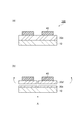
- FIG. 1 is a schematic cross-sectional view for explaining an embodiment of a method for manufacturing a semiconductor device of the present invention
- FIGS. 1A and 1B are schematic cross-sectional views showing each step.
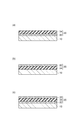
- 2A, 2B, and 2C are schematic cross-sectional views showing an embodiment of the temporary fixing material precursor layer.
- 3(a), (b), (c), and (d) are schematic cross-sectional views showing an embodiment of a laminated body formed using the temporary fixing material precursor layer shown in FIG. 2(a).
- FIG. 4 is a schematic cross-sectional view for explaining one embodiment of a method for manufacturing a semiconductor device of the present invention using the stacked body shown in FIG. 3(d), and FIGS.
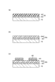
- FIG. 5 is a schematic cross section for demonstrating other embodiment of the manufacturing method of the laminated body shown to Fig.1 (a), and FIG.5(a), (b), and (c) show each process. It is a schematic cross-sectional view showing.
- the numerical range indicated by using “to” indicates the range including the numerical values before and after “to” as the minimum value and the maximum value, respectively.
- the upper limit or the lower limit described in one numerical range may be replaced with the upper limit or the lower limit of the numerical range described in other stages. Good.
- the upper limit value or the lower limit value of the numerical range may be replaced with the value shown in the examples.
- (meth)acrylic acid means acrylic acid or methacrylic acid corresponding thereto.
- the semiconductor device manufacturing method includes a support member, a temporary fixing material layer that absorbs light to generate heat (hereinafter, may be simply referred to as “temporary fixing material layer”), and a semiconductor member. And a separating step of irradiating the temporary fixing material layer in the laminated body with light to separate the semiconductor member from the supporting member.
- FIG. 1 is a schematic cross-sectional view for explaining an embodiment of a method for manufacturing a semiconductor device of the present invention
- FIGS. 1A and 1B are schematic cross-sectional views showing each step.
- a laminated body 100 in which the support member 10, the temporary fixing material layer 30c, and the semiconductor member 40 are laminated in this order is prepared.
- the supporting member 10 is not particularly limited, but may be, for example, a glass substrate, a resin substrate, a silicon wafer, a metal thin film, or the like.
- the support member 10 may be a substrate that does not prevent the transmission of light, or may be a glass substrate.
- the thickness of the support member 10 may be, for example, 0.1 to 2.0 mm. When the thickness is 0.1 mm or more, handling tends to be easy, and when the thickness is 2.0 mm or less, material cost tends to be suppressed.
- the temporary fixing material layer 30c is a layer for temporarily fixing the support member 10 and the semiconductor member 40, and is a layer that absorbs light and generates heat when irradiated with light.
- the light to be absorbed by the temporary fixing material layer 30c may be light including any of infrared light, visible light, and ultraviolet light. Since the light absorption layer described below can efficiently generate heat, the light to be absorbed by the temporary fixing material layer 30c may be light containing at least infrared light.
- the temporary fixing material layer 30c may be a layer that absorbs infrared light and generates heat when irradiated with light including infrared light.
- a temporary fixing material precursor layer is formed on a supporting member, a semiconductor member is arranged on the temporary fixing material precursor layer, and the temporary fixing material precursor layer is cured. It can be prepared by curing the volatile resin component and forming the temporary fixing material layer.
- the temporary fixing material precursor layer has a light absorbing layer that absorbs light to generate heat, and a resin layer containing a curable resin component.
- 2A, 2B, and 2C are schematic cross-sectional views showing an embodiment of the temporary fixing material precursor layer.
- the temporary fixing material precursor layer 30 is not particularly limited in its structure as long as it has the light absorption layer 32 and the resin layer 34, but for example, the light absorption layer 32 and the resin layer 34 are a supporting member.
- the temporary fixing material precursor layer 30 may have a configuration having the light absorption layer 32 and the resin layer 34 in this order from the support member 10 side (FIG. 2A).
- FIG. 2A a mode in which the temporary fixing material precursor layer 30 having the configuration shown in FIG. 2A is mainly used will be described in detail.
- One mode of the light absorption layer 32 may be a layer (hereinafter, referred to as “conductor layer”) including a conductor (hereinafter, may be simply referred to as “conductor”) that absorbs light and generates heat. ).
- the conductor that constitutes such a conductor layer is not particularly limited as long as it is a conductor that absorbs light and generates heat, but may be a conductor that absorbs infrared light and generates heat.
- the conductor include metals such as chromium, copper, titanium, silver, platinum and gold, nickel-chromium, stainless steel, alloys such as copper-zinc, indium tin oxide (ITO), zinc oxide and niobium oxide. Examples thereof include metal oxides and carbon materials such as conductive carbon. These may be used alone or in combination of two or more. Of these, the conductor may be chromium, titanium, copper, aluminum, silver, gold, platinum, or carbon.
- the light absorption layer 32 may be composed of a plurality of conductor layers.
- a light absorption layer for example, the first conductor layer provided on the support member 10 and the second conductor layer provided on the surface of the first conductor layer opposite to the support member 10 are provided.
- a light absorption layer composed of The conductor in the first conductor layer may be titanium from the viewpoint of adhesion with a support member (for example, glass), film formability, thermal conductivity, low heat capacity, and the like.
- the conductor in the second conductor layer may be copper, aluminum, silver, gold, or platinum from the viewpoint of high expansion coefficient, high thermal conductivity, and the like, and among these, copper or aluminum is preferable.
- the conductor layer as the light absorption layer 32 is obtained by subjecting these conductors to physical vapor deposition (PVD) such as vacuum deposition and sputtering, electrolytic plating, electroless plating, and chemical vapor deposition (CVD) such as plasma chemical vapor deposition.
- PVD physical vapor deposition
- CVD chemical vapor deposition
- the conductor layer may be formed by physical vapor deposition, or may be formed by sputtering or vacuum evaporation because the conductor layer can be formed over a large area.
- the thickness of one mode of the light absorption layer 32 may be 1 to 5000 nm (0.001 to 5 ⁇ m) or 50 to 3000 nm (0.05 to 3 ⁇ m) from the viewpoint of light releasability.
- the thickness of the first conductor layer is 1 to 1000 nm, 5 to 500 nm, or 10 to 100 nm.
- the thickness of the second conductor layer may be 1 to 5000 nm, 10 to 500 nm, 30 to 300 nm, or 50 to 200 nm.
- Another mode of the light absorption layer 32 is a layer containing a cured product of a curable resin composition containing conductive particles that absorb light to generate heat.
- the curable resin composition may contain conductive particles and a curable resin component.
- the conductive particles are not particularly limited as long as they absorb light and generate heat, but may be particles that absorb infrared light and generate heat.
- the conductive particles are, for example, silver powder, copper powder, nickel powder, aluminum powder, chrome powder, iron powder, true casting powder, tin powder, titanium alloy, gold powder, alloy copper powder, copper oxide powder, silver oxide powder, tin oxide powder.
- at least one selected from the group consisting of conductive carbon (carbon) powder from the viewpoint of handleability and safety, the conductive particles may be at least one selected from the group consisting of silver powder, copper powder, silver oxide powder, copper oxide powder, and carbon (carbon) powder.
- the conductive particles may be particles in which a resin or a metal is used as a core and the core is plated with a metal such as nickel, gold or silver. Further, the conductive particles may be particles whose surfaces are treated with a surface treatment agent from the viewpoint of dispersibility with a solvent.
- the content of the conductive particles may be 10 to 90 parts by mass with respect to 100 parts by mass of the total amount of components other than the conductive particles of the curable resin composition.
- the components other than the conductive particles of the curable resin composition do not include the organic solvent described below.
- the content of the conductive particles may be 15 parts by mass or more, 20 parts by mass or more, or 25 parts by mass or more.
- the content of the conductive particles may be 80 parts by mass or less or 50 parts by mass or less.
- the curable resin component may be a curable resin component that is cured by heat or light.
- the curable resin component may include, for example, a thermosetting resin, a curing agent, and a curing accelerator.
- a thermosetting resin for example, those exemplified as the curable resin component in the resin layer described later can be used.
- the total content of the thermosetting resin and the curing agent may be 10 to 90 parts by mass based on 100 parts by mass of the total amount of the components other than the conductive particles of the curable resin composition.
- the content of the curing accelerator may be 0.01 to 5 parts by mass with respect to 100 parts by mass of the total amount of the thermosetting resin and the curing agent.
- the light absorption layer 32 can be formed from a curable resin composition containing conductive particles that absorb light and generate heat.
- the curable resin composition may be used as a varnish of the curable resin composition diluted with an organic solvent.
- the organic solvent include acetone, ethyl acetate, butyl acetate, methyl ethyl ketone (MEK), and the like. These organic solvents may be used alone or in combination of two or more.
- the solid component concentration in the varnish may be 10-80% by weight, based on the total weight of the varnish.
- the light absorption layer 32 can be formed by directly applying the curable resin composition to the support member 10.
- a varnish of a curable resin composition diluted with an organic solvent it can be formed by applying the curable resin composition to the support member 10 and heating and drying the solvent to remove.
- the thickness of the light absorbing layer 32 in another embodiment may be 1 to 5000 nm (0.001 to 5 ⁇ m) or 50 to 3000 nm (0.05 to 3 ⁇ m) from the viewpoint of light peeling property.
- the resin layer 34 is formed on the light absorption layer 32.
- the resin layer 34 is a layer that does not contain conductive particles and that contains a curable resin component that is cured by heat or light.
- the resin layer 34 may be a layer made of a curable resin component.
- the curable resin component contains a hydrocarbon resin, and the cured product of the curable resin component has a storage elastic modulus at 25° C. of 5 to 100 MPa. The case where the resin layer 34 is a layer made of a curable resin component will be described in detail below.
- Hydrocarbon resin is a resin whose main skeleton is composed of hydrocarbons.
- hydrocarbon resin examples include ethylene/propylene copolymer, ethylene/1-butene copolymer, ethylene/propylene/1-butene copolymer elastomer, ethylene/1-hexene copolymer, ethylene 1-octene copolymer, ethylene/styrene copolymer, ethylene/norbornene copolymer, propylene/1-butene copolymer, ethylene/propylene/non-conjugated diene copolymer, ethylene/1-butene/non-conjugated diene Copolymer, ethylene/propylene/1-butene/non-conjugated diene copolymer, polyisoprene, polybutadiene, styrene/butadiene/styrene block copolymer (SBS), styrene/
- hydrocarbon resins may be subjected to hydrogenation treatment. Further, these hydrocarbon resins may be carboxy-modified with maleic anhydride or the like.
- the hydrocarbon resin may include a hydrocarbon resin (styrene resin) containing a monomer unit derived from styrene, and includes a styrene/ethylene/butylene/styrene block copolymer (SEBS). Good.
- the Tg of the hydrocarbon resin may be -100 to 500°C, -50 to 300°C, or -50 to 50°C.
- the Tg of the hydrocarbon resin is 500° C. or less, flexibility tends to be easily ensured and the low-temperature sticking property tends to be improved when the film-shaped temporary fixing material is formed.
- the Tg of the hydrocarbon resin is ⁇ 100° C. or higher, when the film-shaped temporary fixing material is formed, it tends to be possible to suppress deterioration in handleability and peelability due to too high flexibility.
- the Tg of a hydrocarbon resin is the midpoint glass transition temperature value obtained by differential scanning calorimetry (DSC).
- the Tg of a hydrocarbon resin is specifically calculated by measuring the change in heat quantity under the conditions of a temperature rising rate of 10°C/min and a measurement temperature of -80 to 80°C, and is calculated by a method according to JIS K 7121. It is the transition temperature.
- the weight average molecular weight (Mw) of the hydrocarbon resin may be 10,000 to 5,000,000 or 100,000 to 2,000,000. When the weight average molecular weight is 10,000 or more, it tends to be easy to secure the heat resistance of the temporary fixing material layer formed. When the weight average molecular weight is 5,000,000 or less, when the film-shaped temporary fixing material layer or the resin layer is formed, it tends to easily suppress a decrease in flow and a decrease in sticking property.
- the weight average molecular weight is a polystyrene conversion value using a calibration curve based on standard polystyrene by gel permeation chromatography (GPC).
- the content of the hydrocarbon resin can be appropriately set so that the cured product of the curable resin component has a storage elastic modulus at 25° C. in the range of 5 to 100 MPa.
- the content of the hydrocarbon resin may be, for example, 40 to 90 parts by mass with respect to 100 parts by mass of the total amount of the curable resin component.
- the content of the hydrocarbon resin may be 50 parts by mass or more or 60 parts by mass or more.
- the content of the hydrocarbon resin may be 85 parts by mass or less or 80 parts by mass or less.
- the curable resin component may include a thermosetting resin in addition to the hydrocarbon resin.
- the thermosetting resin means a resin that is cured by heat, and is a concept that does not include the above hydrocarbon resin.
- the thermosetting resin include epoxy resin, acrylic resin, silicone resin, phenol resin, thermosetting polyimide resin, polyurethane resin, melamine resin, urea resin and the like. These may be used alone or in combination of two or more.
- the thermosetting resin may be an epoxy resin because it is excellent in heat resistance, workability, and reliability. When an epoxy resin is used as the thermosetting resin, it may be used in combination with an epoxy resin curing agent.
- the epoxy resin is not particularly limited as long as it cures and has a heat resistance effect.
- the epoxy resin include bifunctional epoxy resins such as bisphenol A type epoxy, phenol novolac type epoxy resins, and novolac type epoxy resins such as cresol novolac type epoxy resins.
- the epoxy resin may be a polyfunctional epoxy resin, a glycidylamine type epoxy resin, a heterocycle-containing epoxy resin, or an alicyclic epoxy resin.
- the curable resin component may include an epoxy resin curing agent.
- an epoxy resin curing agent a commonly used known curing agent can be used.
- the epoxy resin curing agent include bisphenol and phenol novolac having two or more phenolic hydroxyl groups in one molecule such as amine, polyamide, acid anhydride, polysulfide, boron trifluoride, bisphenol A, bisphenol F, and bisphenol S.
- examples thereof include resins, bisphenol A novolac resins, cresol novolac resins, phenol aralkyl resins, and other phenolic resins.
- the total content of the thermosetting resin and the curing agent may be 10 to 60 parts by mass based on 100 parts by mass of the total amount of the curable resin components.
- the total content of the thermosetting resin and the curing agent may be 15 parts by mass or more or 20 parts by mass or more.
- the total content of the thermosetting resin and the curing agent may be 50 parts by mass or less or 40 parts by mass or less.
- the curable resin component may further contain a curing accelerator.
- the curing accelerator include imidazole derivative, dicyandiamide derivative, dicarboxylic acid dihydrazide, triphenylphosphine, tetraphenylphosphonium tetraphenylborate, 2-ethyl-4-methylimidazole-tetraphenylborate, 1,8-diazabicyclo[5,5] 4,0]undecene-7-tetraphenylborate and the like can be mentioned. These may be used alone or in combination of two or more.
- the content of the curing accelerator may be 0.01 to 5 parts by mass based on 100 parts by mass of the total amount of the thermosetting resin and the curing agent.
- the content of the curing accelerator is within the above range, the curability is improved and the heat resistance tends to be more excellent.
- the curable resin component may further contain a polymerizable monomer and a polymerization initiator.
- the polymerizable monomer is not particularly limited as long as it is polymerized by heating or irradiation with ultraviolet light or the like.
- the polymerizable monomer may be, for example, a compound having a polymerizable functional group such as an ethylenically unsaturated group from the viewpoint of material selectivity and availability.
- Examples of the polymerizable monomer include (meth)acrylate, vinylidene halide, vinyl ether, vinyl ester, vinyl pyridine, vinyl amide, and arylated vinyl. Of these, the polymerizable monomer may be (meth)acrylate.
- the (meth)acrylate may be monofunctional (monofunctional), difunctional, or trifunctional or higher, but may be bifunctional or higher (meth)acrylate from the viewpoint of obtaining sufficient curability. Good.
- Examples of monofunctional (meth)acrylates include (meth)acrylic acid; methyl (meth)acrylate, ethyl (meth)acrylate, butyl (meth)acrylate, isobutyl (meth)acrylate, tert-butyl (meth)acrylate, butoxy.
- Ethyl (meth)acrylate isoamyl (meth)acrylate, hexyl (meth)acrylate, 2-ethylhexyl (meth)acrylate, heptyl (meth)acrylate, octylheptyl (meth)acrylate, nonyl (meth)acrylate, decyl (meth)acrylate 2-hydroxyethyl (meth)acrylate, 2-hydroxypropyl (meth)acrylate, 3-chloro-2-hydroxypropyl (meth)acrylate, 2-hydroxybutyl (meth)acrylate, methoxy polyethylene glycol (meth)acrylate, ethoxy polyethylene Aliphatic (meth)acrylates such as glycol (meth)acrylate, methoxy polypropylene glycol (meth)acrylate, ethoxy polypropylene glycol (meth)acrylate, mono(2-(meth)acryloyloxyethyl)succinate; benzyl (meth
- bifunctional (meth)acrylate examples include ethylene glycol di(meth)acrylate, diethylene glycol di(meth)acrylate, triethylene glycol di(meth)acrylate, tetraethylene glycol di(meth)acrylate, polyethylene glycol di(meth).
- trifunctional or higher polyfunctional (meth)acrylates examples include trimethylolpropane tri(meth)acrylate, ethoxylated trimethylolpropane tri(meth)acrylate, propoxylated trimethylolpropane tri(meth)acrylate, ethoxylated propoxylated Trimethylolpropane tri(meth)acrylate, pentaerythritol tri(meth)acrylate, ethoxylated pentaerythritol tri(meth)acrylate, propoxylated pentaerythritol tri(meth)acrylate, ethoxylated propoxylated pentaerythritol tri(meth)acrylate, penta Erythritol tetra(meth)acrylate, ethoxylated pentaerythritol tetra(meth)acrylate, propoxylated pentaerythritol tetra(meth)acrylate,
- These (meth)acrylates may be used alone or in combination of two or more. Furthermore, these (meth)acrylates may be used in combination with other polymerizable monomers.
- the content of the polymerizable monomer may be 10 to 60 parts by mass with respect to 100 parts by mass of the total amount of the curable resin component.
- the polymerization initiator is not particularly limited as long as it initiates polymerization by heating or irradiation with ultraviolet light.
- the polymerizable initiator may be a thermal radical polymerization initiator or a photo radical polymerization initiator.
- thermal radical polymerization initiator examples include diacyl peroxides such as octanoyl peroxide, lauroyl peroxide, stearyl peroxide and benzoyl peroxide; t-butyl peroxypivalate, t-hexyl peroxypivalate, 1, 1,3,3-Tetramethylbutylperoxy-2-ethylhexanoate, 2,5-Dimethyl-2,5-bis(2-ethylhexanoylperoxy)hexane, t-hexylperoxy-2-ethyl Hexanoate, t-butylperoxy-2-ethylhexanoate, t-butylperoxyisobutyrate, t-hexylperoxyisopropyl monocarbonate, t-butylperoxy-3,5,5-trimethylhexano Ate, t-butylperoxylaurylate, t-butylperoxyis
- photoradical polymerization initiator examples include benzoin ketals such as 2,2-dimethoxy-1,2-diphenylethane-1-one; 1-hydroxycyclohexyl phenyl ketone, 2-hydroxy-2-methyl-1-phenylpropane. ⁇ -hydroxyketones such as 1-one and 1-[4-(2-hydroxyethoxy)phenyl]-2-hydroxy-2-methyl-1-propan-1-one; bis(2,4,6-trimethyl) Examples thereof include benzoyl)phenylphosphine oxide, bis(2,6-dimethoxybenzoyl)-2,4,4-trimethylpentylphosphine oxide, and 2,4,6-trimethylbenzoyldiphenylphosphine oxide.
- benzoin ketals such as 2,2-dimethoxy-1,2-diphenylethane-1-one
- 1-hydroxycyclohexyl phenyl ketone 2-hydroxy-2-methyl-1-phenylpropane.
- ⁇ -hydroxyketones
- These heat and photo radical polymerization initiators may be used alone or in combination of two or more.
- the content of the polymerization initiator may be 0.01 to 5 parts by mass with respect to 100 parts by mass of the total amount of the polymerizable monomers.
- the curable resin component may further include an insulating filler, a sensitizer, an antioxidant, etc. as other components.
- the insulating filler may be added for the purpose of imparting low thermal expansion and low hygroscopicity to the resin layer.
- the insulating filler include non-metal inorganic fillers such as silica, alumina, boron nitride, titania, glass and ceramics. You may use these insulating fillers individually by 1 type or in combination of 2 or more types.
- the insulating filler may be particles whose surface is treated with a surface treatment agent.
- the surface treatment agent the same one as the above-mentioned silane coupling agent can be used.
- the content of the insulating filler may be 5 to 20 parts by mass based on 100 parts by mass of the total amount of the curable resin component.
- heat resistance tends to be further improved without hindering light transmission.
- the content of the insulating filler is within the above range, it may contribute to light peeling property.
- sensitizer examples include anthracene, phenanthrene, chrysene, benzopyrene, fluoranthene, rubrene, pyrene, xanthone, indanthrene, thioxanthen-9-one, 2-isopropyl-9H-thioxanthen-9-one, 4- Examples include isopropyl-9H-thioxanthen-9-one and 1-chloro-4-propoxythioxanthone.
- the content of the sensitizer may be 0.01 to 10 parts by mass based on 100 parts by mass of the total amount of the curable resin component.
- the content of the sensitizer is within the above range, the characteristics of the curable resin component and the effect on the thin film property tend to be small.
- antioxidants examples include quinone derivatives such as benzoquinone and hydroquinone, phenol derivatives such as 4-methoxyphenol and 4-t-butylcatechol, 2,2,6,6-tetramethylpiperidine-1-oxyl, 4- Examples thereof include aminoxyl derivatives such as hydroxy-2,2,6,6-tetramethylpiperidine-1-oxyl and hindered amine derivatives such as tetramethylpiperidyl methacrylate.
- quinone derivatives such as benzoquinone and hydroquinone
- phenol derivatives such as 4-methoxyphenol and 4-t-butylcatechol
- 2,2,6,6-tetramethylpiperidine-1-oxyl 4- Examples thereof include aminoxyl derivatives such as hydroxy-2,2,6,6-tetramethylpiperidine-1-oxyl and hindered amine derivatives such as tetramethylpiperidyl methacrylate.
- the content of the antioxidant may be 0.1 to 10 parts by mass based on 100 parts by mass of the total amount of the curable resin component. When the content of the antioxidant is within the above range, it tends to suppress the decomposition of the curable resin component and prevent contamination.
- the storage elastic modulus at 25° C. of the cured product of the curable resin component is 5 to 100 MPa.
- the cured product of the curable resin component may have a storage elastic modulus at 25° C. of 5.5 MPa or higher, 6 MPa or higher, or 6.3 MPa or higher, and 90 MPa or lower, 80 MPa or lower, 70 MPa or lower, or 65 MPa or lower. Good.
- the storage elastic modulus at 25° C. in the cured product of the curable resin component can be appropriately adjusted. For example, the proportion of the hydrocarbon resin is increased, a hydrocarbon resin having a high Tg is applied, and an insulating filler is added. By doing so, the storage elastic modulus at 25° C.
- cured material of a curable resin component means what was measured by the hardening method and measurement procedure described in an Example.
- the storage elastic modulus at 250° C. in the cured product of the curable resin component is not particularly limited, but may be, for example, 0.70 to 2.00 MPa.
- the storage elastic modulus at 250° C. in the cured product of the curable resin component may be 0.80 MPa or higher, 0.85 MPa or higher, or 0.90 MPa or higher, and may be 1.90 MPa or lower, 1.80 MPa or lower, or 1. It may be 75 MPa or less.
- the resin layer 34 can be formed from a curable resin component containing a hydrocarbon resin (curable resin composition containing no conductive particles).
- the curable resin component may be used as a varnish of the curable resin component diluted with a solvent.
- the solvent is not particularly limited as long as it can dissolve components other than the insulating filler. Examples of the solvent include aromatic hydrocarbons such as toluene, xylene, mesitylene, cumene and p-cymene; aliphatic hydrocarbons such as hexane and heptane; cyclic alkanes such as methylcyclohexane; tetrahydrofuran, 1,4-dioxane and the like.
- Cyclic ethers such as acetone, methyl ethyl ketone, methyl isobutyl ketone, cyclohexanone, 4-hydroxy-4-methyl-2-pentanone; esters such as methyl acetate, ethyl acetate, butyl acetate, methyl lactate, ethyl lactate, ⁇ -butyrolactone; Carbonic acid esters such as ethylene carbonate and propylene carbonate; amides such as N,N-dimethylformamide, N,N-dimethylacetamide and N-methyl-2-pyrrolidone. These solvents may be used alone or in combination of two or more.
- the solvent may be toluene, xylene, heptane, or cyclohexane from the viewpoint of solubility and boiling point.
- the solid component concentration in the varnish may be 10-80% by weight, based on the total weight of the varnish.
- the curable resin component varnish can be prepared by mixing and kneading a curable resin component containing a hydrocarbon resin and a solvent. Mixing and kneading can be carried out by appropriately combining an ordinary stirrer, a raker, a three-roller, a bead mill and other dispersers.
- the resin layer 34 can be formed by directly applying a curable resin component to the light absorption layer 32.
- the varnish of the curable resin component diluted with the solvent it can be formed by applying the varnish of the curable resin component to the light absorption layer 32 and heating and drying the solvent to remove.
- the resin layer 34 can also be formed by producing a curable resin component film made of a curable resin component.
- the thickness of the resin layer 34 can be adjusted according to the thickness of the temporary fixing material layer 20.
- the thickness of the resin layer 34 may be, for example, 50 ⁇ m or less from the viewpoint of stress relaxation.
- the resin layer 34 may have a thickness of 0.1 to 40 ⁇ m or 1 to 30 ⁇ m.
- a laminated film having a light absorbing layer 32 and a resin layer 34 (hereinafter, may be referred to as “temporary fixing material laminated film”) is prepared in advance, and the light absorbing layer 32 is prepared. It can also be produced by laminating the support member 10 and the support member 10 in contact with each other.
- the configurations of the light absorbing layer 32 and the resin layer 34 in the laminated film for temporary fixing material are not particularly limited as long as they have the light absorbing layer 32 and the resin layer 34, but for example, the light absorbing layer A configuration including 32 and the resin layer 34, a configuration including the light absorption layer 32, the resin layer 34, and the light absorption layer 32 in this order, and the like can be given.
- the laminated film for temporary fixing material may have a configuration including the light absorption layer 32 and the resin layer 34.
- the light absorption layer 32 may be a layer made of a conductor (conductor layer) or a layer containing conductive particles.
- the laminated film for temporary fixing material may be provided on the support film, and if necessary, a protective film may be provided on the surface opposite to the support film.
- the support film is not particularly limited, and examples thereof include polyesters such as polyethylene terephthalate (PET), polybutylene terephthalate and polyethylene naphthalate; polyolefins such as polyethylene and polypropylene; polycarbonate, polyamide, polyimide, polyamideimide, polyetherimide, poly Examples thereof include ether sulfide, polyether sulfone, polyether ketone, polyphenylene ether, polyphenylene sulfide, poly(meth)acrylate, polysulfone, and liquid crystal polymer film. These may be subjected to a mold release treatment.
- the thickness of the support film may be, for example, 3 to 250 ⁇ m.
- the protective film examples include polyesters such as polyethylene terephthalate, polybutylene terephthalate and polyethylene naphthalate; polyolefins such as polyethylene and polypropylene.
- the thickness of the protective film may be, for example, 10 to 250 ⁇ m.
- the thickness of the light absorption layer 32 in the laminated film for temporary fixing material may be 1 to 5000 nm (0.001 to 5 ⁇ m) or 50 to 3000 nm (0.05 to 3 ⁇ m) from the viewpoint of light releasability.
- the thickness of the resin layer 34 in the temporary fixing material laminated film may be, for example, 50 ⁇ m or less.
- the resin layer 34 may have a thickness of 0.1 to 40 ⁇ m or 1 to 30 ⁇ m.
- the thickness of the temporary fixing material laminated film can be adjusted according to the desired thickness of the temporary fixing material layer.
- the laminated film for temporary fixing material may have a thickness of 0.1 to 55 ⁇ m or 10 to 40 ⁇ m from the viewpoint of stress relaxation.
- the temporary fixing material precursor layer 30 having the configuration shown in FIG. 2B can be produced by, for example, forming the resin layer 34 on the supporting member 10 and then forming the light absorption layer 32.
- the temporary fixing material precursor layer 30 having the configuration shown in FIG. 2C can be produced, for example, by alternately forming the light absorption layers 32, the resin layers 34, and the light absorption layers 32 on the support member 10. it can.
- These temporary fixing material precursor layers 30 may be prepared by preparing the laminated film for temporary fixing material having the above-mentioned configuration in advance and laminating it on the supporting member 10.
- the thickness of the temporary fixing material precursor layer 30 (the total thickness of the light absorbing layer 32 and the resin layer 34) may be the same as the thickness of the above-mentioned temporary fixing material laminated film.
- a semiconductor member is arranged on the prepared temporary fixing material precursor layer, the curable resin component in the temporary fixing material precursor layer 30 (resin layer 34) is cured, and the light absorbing layer and the curable resin component are cured.
- a temporary fixing material layer having a resin cured product layer containing a material
- a laminated body in which the support member 10, the temporary fixing material layer 30c, and the semiconductor member 40 are laminated in this order is manufactured (FIG. )).
- 3(a), (b), (c), and (d) are schematic cross-sectional views showing an embodiment of a laminated body formed using the temporary fixing material precursor layer shown in FIG. 2(a). Is.
- the semiconductor member 40 may be a semiconductor wafer or a semiconductor chip obtained by cutting the semiconductor wafer into a predetermined size and dividing the semiconductor wafer into chips. When a semiconductor chip is used as the semiconductor member 40, a plurality of semiconductor chips are usually used.
- the thickness of the semiconductor member 40 may be 1 to 1000 ⁇ m, 10 to 500 ⁇ m, or 20 to 200 ⁇ m from the viewpoints of reducing the size and thickness of the semiconductor device and suppressing cracking during transportation, processing steps and the like. ..
- the semiconductor wafer or the semiconductor chip may be provided with a rewiring layer, a pattern layer, or an external connection member having an external connection terminal.
- the supporting member 10 provided with the prepared temporary fixing material precursor layer 30 is placed on a vacuum press or a vacuum laminator, and the semiconductor member 40 is placed on the temporary fixing material precursor layer 30 and pressed. It can be laminated by pressure bonding with.
- the semiconductor member 40 is pressure bonded to the temporary fixing material precursor layer 30 at an atmospheric pressure of 1 hPa or less, a pressure bonding pressure of 1 MPa, a pressure bonding temperature of 120 to 200° C., and a holding time of 100 to 300 seconds.
- the pressure is 1 hPa or less
- the pressure bonding temperature is 60 to 180° C. or 80 to 150° C.
- the laminating pressure is 0.01 to 0.5 MPa or 0.1 to 0.5 MPa
- the holding time is 1 to 600 seconds
- the semiconductor member 40 is pressure-bonded to the temporary fixing material precursor layer 30 for 30 to 300 seconds.
- the curable resin component in the temporary fixing material precursor layer 30 is thermally cured or photocured under predetermined conditions.
- the conditions for heat curing may be, for example, 300° C. or lower or 100 to 200° C. for 1 to 180 minutes or 1 to 60 minutes.
- the cured product of the curable resin component is formed, and the semiconductor member 40 is temporarily fixed to the support member 10 via the temporary fixing material layer 30c containing the cured product of the curable resin component, and the laminated body 300 is obtained. can get.
- the temporary fixing material layer 30c can be composed of a light absorbing layer 32 and a resin cured product layer 34c containing a cured product of a curable resin component.
- the laminated body can also be produced, for example, by forming a temporary fixing material layer and then disposing a semiconductor member.
- FIG. 5 is a schematic cross section for demonstrating other embodiment of the manufacturing method of the laminated body shown to Fig.1 (a), and FIG.5(a), (b), and (c) show each process. It is a schematic cross-sectional view showing.
- Each step of FIG. 5 uses the temporary fixing material precursor layer shown in FIG.
- the laminate forms the temporary fixing material precursor layer 30 containing the curable resin component on the supporting member 10 (FIG. 5A), and the curable resin component in the temporary fixing material precursor layer 30 (resin layer 34).
- a temporary fixing material layer 30c containing a cured product of a curable resin component (FIG. 5B), and disposing the semiconductor member 40 on the formed temporary fixing material layer 30c. It is possible (Fig. 5(c)).
- the wiring layer 41 such as a rewiring layer or a pattern layer can be provided on the temporary fixing material layer 20c before disposing the semiconductor member 40, the semiconductor member 40 is formed on the wiring layer 41. By disposing, the semiconductor member 40 having the wiring layer 41 can be formed.
- the semiconductor member 40 (semiconductor member 40 temporarily fixed to the support member 10) in the stacked body 100 may be further processed.
- the laminated bodies 310 (FIG. 3B), 320 (FIG. 3C), 330 (FIG. 3D), etc. can get.
- the processing of the semiconductor member is not particularly limited, and examples thereof include thinning of the semiconductor member, production of through electrodes, formation of wiring layers such as rewiring layers and pattern layers, etching treatment, plating reflow treatment, and sputtering treatment. ..
- the thinning of the semiconductor member can be performed by grinding the surface of the semiconductor member 40 opposite to the surface in contact with the temporary fixing material layer 30c with a grinder or the like.
- the thinned semiconductor member may have a thickness of, for example, 100 ⁇ m or less.
- the grinding conditions can be arbitrarily set according to the desired thickness of the semiconductor member, the grinding state, and the like.
- the through electrode is manufactured by performing a process such as dry ion etching or a Bosch process on the surface of the thinned semiconductor member 40 opposite to the surface in contact with the temporary fixing material layer 30c to form a through hole. It can be performed by treatment such as copper plating.
- the semiconductor member 40 is processed, and for example, the semiconductor member 40 is thinned to obtain the laminated body 310 (FIG. 3B) provided with the through electrode 44.
- the laminated body 310 shown in FIG. 3B may be covered with the sealing layer 50 as shown in FIG.
- the material of the sealing layer 50 is not particularly limited, but may be a thermosetting resin composition from the viewpoint of heat resistance and other reliability.
- the thermosetting resin used for the sealing layer 50 include epoxy resins such as cresol novolac epoxy resin, phenol novolac epoxy resin, biphenyl diepoxy resin, and naphthol novolac epoxy resin.
- An additive such as a filler and/or a flame retardant substance such as a bromine compound may be added to the composition for forming the sealing layer 50.
- the supply form of the sealing layer 50 is not particularly limited, but may be a solid material, a liquid material, a fine grain material, a film material, or the like.
- the sealing layer 50 formed of the sealing film for example, a compression sealing molding machine, a vacuum laminating apparatus, etc. are used. Using the above apparatus, for example, a heat-sealed seal under the conditions of 40 to 180° C. (or 60 to 150° C.), 0.1 to 10 MPa (or 0.5 to 8 MPa), and 0.5 to 10 minutes.
- the sealing layer 50 can be formed by covering the processed semiconductor member 42 with a stop film.
- the sealing film may be prepared in a state of being laminated on a release liner such as a polyethylene terephthalate (PET) film.
- PET polyethylene terephthalate
- the sealing layer 50 can be formed by disposing the sealing film on the processed semiconductor member 42, embedding the processed semiconductor member 42, and then peeling off the release liner. In this way, the laminated body 320 shown in FIG. 3C can be obtained.
- the thickness of the encapsulation film is adjusted so that the encapsulation layer 50 has a thickness equal to or greater than the thickness of the processed semiconductor member 42.
- the thickness of the sealing film may be 50 to 2000 ⁇ m, 70 to 1500 ⁇ m, or 100 to 1000 ⁇ m.
- the processed semiconductor member 42 having the sealing layer 50 may be diced into individual pieces as shown in FIG. In this way, the laminated body 330 shown in FIG. 3D can be obtained.
- the dicing into individual pieces may be carried out after the semiconductor member separating step described later.
- FIG. 4 is a schematic cross-sectional view for explaining one embodiment of a method for manufacturing a semiconductor device of the present invention using the stacked body shown in FIG. 3(d), and FIGS. 4(a) and 4(b) are It is a schematic cross section which shows each process.
- the light absorption layer 32 absorbs the light and instantaneously generates heat.
- the resin cured material layer 34c is melted, and the support member 10 and the semiconductor. Stress with the member 40 (processed semiconductor member 42), scattering of the light absorption layer 32, and the like may occur. Due to the occurrence of such a phenomenon, the temporarily fixed processed semiconductor member 42 can be easily separated (peeled) from the support member 10. In the separation step, a slight stress may be applied to the processed semiconductor member 42 in the direction parallel to the main surface of the support member 10 together with the irradiation of light.
- the light in the separation process may be incoherent light.
- the incoherent light is an electromagnetic wave having properties such that interference fringes do not occur, coherence is low, and directivity is low, and tends to be attenuated as the optical path length becomes longer.
- Incoherent light is light that is not coherent light.
- Laser light is generally coherent light, while light such as sunlight and fluorescent light is incoherent light.
- Incoherent light can also be referred to as light other than laser light. Since the irradiation area of incoherent light is overwhelmingly wider than that of coherent light (that is, laser light), the number of times of irradiation can be reduced (for example, once).
- the light in the separation step may be light containing at least infrared light.
- the light source of light in the separation step is not particularly limited, but may be a xenon lamp.
- a xenon lamp is a lamp that utilizes light emission by applying and discharging an arc tube filled with xenon gas. Since the xenon lamp discharges while repeating ionization and excitation, it has a continuous wavelength from the ultraviolet light region to the infrared light region stably. Since a xenon lamp requires a shorter time to start than a lamp such as a metal halide lamp, the time required for the process can be significantly shortened.
- the irradiation conditions with the xenon lamp can be set arbitrarily such as applied voltage, pulse width, irradiation time, irradiation distance (distance between light source and temporary fixing material layer), irradiation energy.
- the irradiation condition by the xenon lamp may be set so that it can be separated by one irradiation or may be set so as to be separated by two or more irradiations, but from the viewpoint of reducing damage to the processed semiconductor member 42.
- the irradiation condition with the xenon lamp may be set so that it can be separated by one irradiation.
- the separating step may be a step of irradiating the temporary fixing material layer 30c with light via the support member 10 (direction A in FIG. 4A). That is, the irradiation of the temporary fixing material layer 30c with light may be irradiation from the support member 10 side. By irradiating the temporary fixing material layer 30c with light via the support member 10, it becomes possible to irradiate the entire temporary fixing material layer 30c.
- the residue 30c′ (FIGS. 4A and 4B) of the temporary fixing material layer adheres to the semiconductor member 40 or the processed semiconductor member 42. If so, they can be washed with a solvent.
- the solvent is not particularly limited, and examples thereof include ethanol, methanol, toluene, xylene, acetone, methyl ethyl ketone, methyl isobutyl ketone, and hexane. These may be used alone or in combination of two or more. Further, it may be immersed in these solvents, or ultrasonic cleaning may be performed. Furthermore, you may heat within the range of 100 degreeC or less.
- a semiconductor element 60 including the semiconductor member 40 or the processed semiconductor member 42 can be obtained (FIG. 4B).
- a semiconductor device can be manufactured by connecting the obtained semiconductor element 60 to another semiconductor element or a semiconductor element mounting substrate.
- the laminated film having a storage elastic modulus at 5° C. of 5 to 100 MPa can be suitably used as a temporary fixing material for temporarily fixing the semiconductor member to the supporting member.
- Example 1 ⁇ Preparation of curable resin component> 70 parts by mass of maleic anhydride-modified styrene/ethylene/butylene/styrene block copolymer (trade name: FG1924, Clayton Polymer Japan Co., Ltd., styrene content: 13% by mass) as a hydrocarbon resin, and dicyclopentadiene as an epoxy resin 30 parts by weight of a type epoxy resin (trade name: HP7200, DIC Corporation) and 1 part by weight of 1-benzyl-2-methylimidazole (trade name: Cureazole 1B2MZ, Shikoku Chemicals Co., Ltd.) as a curing accelerator To give a mixture.
- a type epoxy resin trade name: HP7200, DIC Corporation
- 1-benzyl-2-methylimidazole trade name: Cureazole 1B2MZ, Shikoku Chemicals Co., Ltd.
- the hydrocarbon resin used was diluted with toluene to a solid content of 25% by mass. These were stirred at 2200 rpm for 10 minutes using an automatic stirrer to prepare a varnish of a curable resin component diluted with toluene as a solvent.
- the thickness of the resulting varnish of the curable resin component was 20 ⁇ m on the release treated surface of a polyethylene terephthalate (PET) film (Purex A31, Teijin DuPont Films Ltd., thickness: 38 ⁇ m) using a precision coating machine. It was applied as described above, heated at 90° C. for 10 minutes, the solvent was dried and removed, and a curable resin component film (resin layer) having a thickness of 20 ⁇ m was produced. Further, coating was performed so as to have a thickness of 200 ⁇ m, heating was performed at 90° C. for 15 to 20 minutes, the solvent was dried and removed, and a curable resin component film (resin layer) having a thickness of 200 ⁇ m was produced.
- PET polyethylene terephthalate
- the obtained curable resin component film having a thickness of 200 ⁇ m was cut into a predetermined size (length (distance between chucks) 20 mm ⁇ width 5.0 mm) and cut in a clean oven (manufactured by ESPEC CORPORATION) at 180° C. for 2 hours.
- a measurement sample which is a cured product (resin cured product layer) of the curable resin component film was obtained.
- the storage elastic moduli at 25° C. and 250° C. in the cured product (resin cured product layer) of the curable resin component film were measured under the following conditions. The results are shown in Table 2.
- Dynamic viscoelasticity measuring device (TA Instruments, RSA-G2) Measurement temperature range: -70 to 300°C Temperature rising rate: 5°C/min Frequency: 1 Hz Measurement mode: Tensile mode
- a light absorbing layer having titanium as the first conductor layer and copper as the second conductor layer was formed by sputtering, A support member having an absorption layer was obtained.
- the light absorption layer is shown in Table 1 after pretreatment by reverse sputtering (Ar flow rate: 1.2 ⁇ 10 ⁇ 2 Pa ⁇ m 3 /s (70 sccm), RF power: 300 W, time: 300 seconds). RF sputtering was performed under the processing conditions, and the titanium layer/copper layer was formed to a thickness of 50 nm/200 nm.
- a curable resin component film (resin layer) having a thickness of 20 ⁇ m was cut into a size of 40 mm ⁇ 40 mm.
- the obtained curable resin component film (resin layer) was placed on the light absorbing layer of the supporting member having the obtained light absorbing layer, and vacuum lamination was performed to obtain the resin of Example 1 provided on the supporting member.
- a laminated film for temporary fixing material was produced.
- a semiconductor chip (size: 10 mm ⁇ 10 mm, thickness: 150 ⁇ m), which is a semiconductor member, was mounted on the curable resin component film (resin layer) of the obtained laminated film for temporary fixing material, and the condition was 180° C. for 1 hour.
- the laminate of Example 1 was obtained by thermosetting.
- Example 2 35 parts by mass of the hydrocarbon resin of Example 1 with maleic anhydride-modified styrene/ethylene/butylene/styrene block copolymer (trade name: FG1924, Clayton Polymer Japan, Inc., styrene content 13% by mass) and maleic anhydride Curable, in the same manner as in Example 1 except that the modified styrene/ethylene/butylene/styrene block copolymer (trade name: FG1901, Clayton Polymer Japan Co., Ltd., styrene content 30% by mass) was changed to 35 parts by mass.
- the storage elastic moduli of 25° C. and 250° C. in the cured product (resin cured product layer) of the resin component film were measured to prepare the laminated film for temporary fixing material and the laminated body of Example 2.
- the results of storage elastic modulus at 25° C. and 250° C. are shown in Table 2.
- Example 3 A cured product of a curable resin component film in the same manner as in Example 1 except that 10% by mass of a silica filler (trade name: R972, Nippon Aerosil Co., Ltd.) was added based on the total amount of the hydrocarbon resin and the epoxy resin.
- a silica filler trade name: R972, Nippon Aerosil Co., Ltd.
- the storage elastic modulus at 25° C. and 250° C. in the (resin cured material layer) was measured to prepare a laminated film for temporary fixing material and a laminated body of Example 3.
- the results of storage elastic modulus at 25° C. and 250° C. are shown in Table 2.
- Example 1 Example except that the epoxy resin used in Example 1 was changed to 30 parts by mass of 3′,4′-epoxycyclohexylmethyl-3,4-epoxycyclohexanecarboxylate (trade name: Celoxide 2021P, Daicel Corporation) In the same manner as in 1, the storage elastic modulus at 25° C. and 250° C. in the cured product (cured resin layer) of the curable resin component film was measured, and the laminated film for temporary fixing material and the laminated body of Comparative Example 1 were produced. .. The results of storage elastic modulus at 25° C. and 250° C. are shown in Table 2.
- Comparative example 2 In the same manner as in Example 1 except that the mass ratio of the hydrocarbon resin and the epoxy resin was changed from 70:30 to 80:20, 25° C. in the cured product (resin cured product layer) of the curable resin component film and The storage elastic modulus at 250° C. was measured to prepare a laminated film for temporary fixing material and a laminated body of Comparative Example 2. The results of storage elastic modulus at 25° C. and 250° C. are shown in Table 2.
- Example 3 The hydrocarbon resin of Example 1 was changed to 70 parts by mass of maleic anhydride-modified styrene/ethylene/butylene/styrene block copolymer (trade name: FG1901, Kraton Polymer Japan Co., Ltd., styrene content 30% by mass).
- FG1901 Kraton Polymer Japan Co., Ltd., styrene content 30% by mass.
- the storage elastic modulus at 25° C. and 250° C. in the cured product (resin cured product layer) of the curable resin component film was measured, and the laminated film for temporary fixing material and the laminate in Example 2 were measured.
- the body was made.
- Table 2 The results of storage elastic modulus at 25° C. and 250° C. are shown in Table 2.
- ⁇ Peelability test> Two laminated bodies were prepared. An applied voltage of 3800 V, a pulse width of 200 ⁇ s, an irradiation distance of 50 mm, an irradiation number of 1 and an irradiation time of 200 ⁇ s, and an applied voltage of 2700 V, a pulse width of 1000 ⁇ s, an irradiation distance of 50 mm, an irradiation number of 1 and an irradiation time of 1000 ⁇ s.
- the laminate was irradiated with a xenon lamp under each of two irradiation conditions of irradiation condition B, and the releasability from the supporting member was evaluated. Xenon lamp, Xenon Corp.
- S2300 (wavelength range: 270 nm ⁇ near infrared region, per unit area irradiation energy: 7J / cm 2 (predicted value, irradiation condition A), 13J / cm 2 (predicted value, the irradiation conditions B)) was used and the xenon lamp irradiation was performed from the support member (slide glass) side of the laminate.
- the irradiation distance is the distance between the light source and the stage on which the slide glass is installed.
- the peelability test was evaluated as "A" when the semiconductor chip spontaneously peeled from the slide glass after irradiation with a xenon lamp, and tweezers were inserted between the semiconductor chip and the slide glass under either irradiation condition. At that time, the case where the semiconductor chip was separated without being damaged was evaluated as "B”, and the case where the semiconductor chip was not separated under any irradiation condition was evaluated as "C”. The results are shown in Table 2.
- the laminates of Examples 1 to 3 in which the cured product of the curable resin component has a storage elastic modulus at 25° C. of 5 to 100 MPa have storage elastic properties of the cured product of the curable resin component at 25° C.
- the peelability from the support member was excellent as compared with the laminates of Comparative Examples 1 to 3 in which the rate did not satisfy the above requirements. From the above results, it was confirmed that the semiconductor device manufacturing method of the present invention can easily separate the temporarily fixed semiconductor member from the supporting member.
Landscapes
- Chemical & Material Sciences (AREA)
- Organic Chemistry (AREA)
- Laminated Bodies (AREA)
- Dicing (AREA)
- Adhesives Or Adhesive Processes (AREA)
Abstract
Description
本実施形態に係る半導体装置の製造方法は、支持部材と、光を吸収して熱を発生する仮固定材層(以下、単に「仮固定材層」という場合がある。)と、半導体部材とがこの順に積層された積層体を準備する準備工程と、積層体における仮固定材層に光を照射して、支持部材から半導体部材を分離する分離工程とを備える。
図1は、本発明の半導体装置の製造方法の一実施形態を説明するための模式断面図であり、図1(a)及び(b)は、各工程を示す模式断面図である。図1(a)に示すとおり、積層体の準備工程においては、支持部材10と、仮固定材層30cと、半導体部材40とがこの順に積層された積層体100を準備する。
図1(b)に示すとおり、半導体部材の分離工程においては、積層体100における仮固定材層30cに方向Aで光を照射して、支持部材10から半導体部材40を分離する。
上述の光を吸収して熱を発生する光吸収層と、硬化性樹脂成分を含む樹脂層とを有し、硬化性樹脂成分が、炭化水素樹脂を含み、硬化性樹脂成分の硬化物における25℃の貯蔵弾性率が、5~100MPaである積層フィルムは、半導体部材を支持部材に仮固定するための仮固定材として好適に用いることができる。
<硬化性樹脂成分の調製>
炭化水素樹脂として、無水マレイン酸変性スチレン・エチレン・ブチレン・スチレンブロック共重合体(商品名:FG1924、クレイトンポリマージャパン株式会社、スチレン含有量13質量%)70質量部、エポキシ樹脂として、ジシクロペンタジエン型エポキシ樹脂(商品名:HP7200、DIC株式会社)30質量部、及び硬化促進剤として、1-ベンジル-2-メチルイミダゾール(商品名:キュアゾール1B2MZ、四国化成工業株式会社)1質量部を混合して混合物を得た。なお、炭化水素樹脂はトルエンで固形分25質量%に希釈したものを用いた。これらを、自動撹拌装置を用いて、2200回転/分で10分間撹拌することによって、溶剤としてのトルエンで希釈された硬化性樹脂成分のワニスを調製した。
得られた硬化性樹脂成分のワニスを、精密塗工機を用いて、ポリエチレンテレフタレート(PET)フィルム(ピューレックスA31、帝人デュポンフィルム株式会社、厚み:38μm)の離型処理面に厚みが20μmとなるように塗工し、90℃で10分間加熱して、溶剤を乾燥除去し、厚みが20μmである硬化性樹脂成分フィルム(樹脂層)を作製した。また、厚みが200μmとなるように塗工し、90℃で15~20分間加熱して、溶剤を乾燥除去し、厚みが200μmである硬化性樹脂成分フィルム(樹脂層)を作製した。
得られた厚みが200μmである硬化性樹脂成分フィルムを、所定のサイズ(縦(チャック間距離)20mm×横5.0mm)に切り出し、クリーンオーブン(エスペック株式会社製)中で180℃、2時間の条件で熱硬化させることによって、硬化性樹脂成分フィルムの硬化物(樹脂硬化物層)である測定サンプルを得た。硬化性樹脂成分フィルムの硬化物(樹脂硬化物層)における25℃及び250℃の貯蔵弾性率を、以下の条件で測定した。結果を表2に示す。
測定温度領域:-70~300℃
昇温速度:5℃/分
周波数:1Hz
測定モード:引張モード
支持部材であるスライドガラス(サイズ:40mm×40mm、厚み:0.8μm)上にスパッタで第1の導電体層がチタン、第2の導電体層が銅である光吸収層を作製し、光吸収層を備える支持部材を得た。なお、当該光吸収層は、逆スパッタリングによる前処理(Ar流速:1.2×10⁻²Pa・m3/s(70sccm)、RF電力:300W、時間:300秒間)後、表1に示す処理条件でRFスパッタリングを行い、チタン層/銅層の厚みを50nm/200nmとすることによって作製した。

厚みが20μmである硬化性樹脂成分フィルム(樹脂層)を40mm×40mmに切り出した。得られた光吸収層を備える支持部材の光吸収層上に、切り出した硬化性樹脂成分フィルム(樹脂層)を配置し、真空ラミネートを行うことによって、支持部材上に設けられた実施例1の仮固定材用積層フィルムを作製した。
得られた仮固定材用積層フィルムの硬化性樹脂成分フィルム(樹脂層)上に、半導体部材である半導体チップ(サイズ:10mm×10mm、厚み:150μm)を搭載し、180℃で1時間の条件で熱硬化させることによって、実施例1の積層体を得た。
実施例1の炭化水素樹脂を、無水マレイン酸変性スチレン・エチレン・ブチレン・スチレンブロック共重合体(商品名:FG1924、クレイトンポリマージャパン株式会社、スチレン含有量13質量%)35質量部及び無水マレイン酸変性スチレン・エチレン・ブチレン・スチレンブロック共重合体(商品名:FG1901、クレイトンポリマージャパン株式会社、スチレン含有量30質量%)35質量部に変更した以外は、実施例1と同様にして、硬化性樹脂成分フィルムの硬化物(樹脂硬化物層)における25℃及び250℃の貯蔵弾性率を測定し、実施例2の仮固定材用積層フィルム及び積層体を作製した。25℃及び250℃の貯蔵弾性率の結果を表2に示す。
炭化水素樹脂及びエポキシ樹脂の全量を基準として10質量%のシリカフィラー(商品名:R972、日本アエロジル株式会社)を加えた以外は、実施例1と同様にして、硬化性樹脂成分フィルムの硬化物(樹脂硬化物層)における25℃及び250℃の貯蔵弾性率を測定し、実施例3の仮固定材用積層フィルム及び積層体を作製した。25℃及び250℃の貯蔵弾性率の結果を表2に示す。
実施例1で使用したエポキシ樹脂を、3’,4’-エポキシシクロヘキシルメチル-3,4-エポキシシクロヘキサンカルボキシレート(商品名:セロキサイド2021P、株式会社ダイセル)30質量部に変更した以外は、実施例1と同様にして、硬化性樹脂成分フィルムの硬化物(樹脂硬化物層)における25℃及び250℃の貯蔵弾性率を測定し、比較例1の仮固定材用積層フィルム及び積層体を作製した。25℃及び250℃の貯蔵弾性率の結果を表2に示す。
炭化水素樹脂とエポキシ樹脂との質量比を70:30から80:20に変更した以外は、実施例1と同様にして、硬化性樹脂成分フィルムの硬化物(樹脂硬化物層)における25℃及び250℃の貯蔵弾性率を測定し、比較例2の仮固定材用積層フィルム及び積層体を作製した。25℃及び250℃の貯蔵弾性率の結果を表2に示す。
実施例1の炭化水素樹脂を、無水マレイン酸変性スチレン・エチレン・ブチレン・スチレンブロック共重合体(商品名:FG1901、クレイトンポリマージャパン株式会社、スチレン含有量30質量%)70質量部に変更した以外は、実施例1と同様にして、硬化性樹脂成分フィルムの硬化物(樹脂硬化物層)における25℃及び250℃の貯蔵弾性率を測定し、実施例2の仮固定材用積層フィルム及び積層体を作製した。25℃及び250℃の貯蔵弾性率の結果を表2に示す。
積層体をそれぞれ2つ用意した。印加電圧3800V、パルス幅200μs、照射距離50mm、照射回数1回、及び照射時間200μsの照射条件A、並びに、印加電圧2700V、パルス幅1000μs、照射距離50mm、照射回数1回、及び照射時間1000μsの照射条件Bの2種類の照射条件でそれぞれ積層体をキセノンランプで照射し、支持部材からの剥離性を評価した。キセノンランプは、Xenon社製のS2300(波長範囲:270nm~近赤外領域、単位面積あたりの照射エネルギー:7J/cm2(予測値、照射条件A)、13J/cm2(予測値、照射条件B))を用い、キセノンランプ照射は、積層体の支持部材(スライドガラス)側から行った。照射距離は、光源とスライドガラスを設置したステージとの距離である。剥離性試験の評価は、キセノンランプ照射後、自然に半導体チップがスライドガラスから剥離した場合を「A」と評価し、いずれかの照射条件で半導体チップとスライドガラスとの間にピンセットを差し込んだときに、半導体チップが破損することなく、分離した場合を「B」と評価し、いずれかの照射条件で分離しなかった場合を「C」と評価した。結果を表2に示す。

Claims (7)
- 支持部材と、光を吸収して熱を発生する仮固定材層と、半導体部材とがこの順に積層された積層体を準備する準備工程と、
前記積層体における前記仮固定材層に光を照射して、前記支持部材から前記半導体部材を分離する分離工程と、
を備え、
前記仮固定材層が、光を吸収して熱を発生する光吸収層と、硬化性樹脂成分の硬化物を含む樹脂硬化物層とを有し、
前記硬化性樹脂成分が、炭化水素樹脂を含み、
前記硬化性樹脂成分の硬化物における25℃の貯蔵弾性率が、5~100MPaである、半導体装置の製造方法。 - 前記分離工程における前記光の光源が、キセノンランプである、請求項1に記載の半導体装置の製造方法。
- 前記分離工程における前記光が、少なくとも赤外光を含む光である、請求項1又は2に記載の半導体装置の製造方法。
- 前記分離工程が、前記支持部材を介して前記仮固定材層に前記光を照射する工程である、請求項1~3のいずれか一項に記載の半導体装置の製造方法。
- 前記硬化性樹脂成分が、熱硬化性樹脂をさらに含む、請求項1~4のいずれか一項に記載の半導体装置の製造方法。
- 半導体部材を支持部材に仮固定するための仮固定材用積層フィルムであって、
光を吸収して熱を発生する光吸収層と、硬化性樹脂成分を含む樹脂層とを有し、
前記硬化性樹脂成分が、炭化水素樹脂を含み、
前記硬化性樹脂成分の硬化物における25℃の貯蔵弾性率が、5~100MPaである、仮固定材用積層フィルム。 - 前記樹脂層の厚みが、50μm以下である、請求項6に記載の仮固定材用積層フィルム。
Priority Applications (4)
| Application Number | Priority Date | Filing Date | Title |
|---|---|---|---|
| US17/296,547 US20220028722A1 (en) | 2018-11-29 | 2019-11-27 | Semiconductor device production method and laminate film for temporary fixation material |
| CN201980078058.9A CN113169058A (zh) | 2018-11-29 | 2019-11-27 | 半导体装置的制造方法及临时固定材料用层叠膜 |
| KR1020217016636A KR102609674B1 (ko) | 2018-11-29 | 2019-11-27 | 반도체 장치의 제조 방법 및 가고정재용 적층 필름 |
| JP2020557801A JP7414005B2 (ja) | 2018-11-29 | 2019-11-27 | 半導体装置の製造方法及び仮固定材用積層フィルム |
Applications Claiming Priority (2)
| Application Number | Priority Date | Filing Date | Title |
|---|---|---|---|
| JP2018-223448 | 2018-11-29 | ||
| JP2018223448 | 2018-11-29 |
Publications (1)
| Publication Number | Publication Date |
|---|---|
| WO2020111154A1 true WO2020111154A1 (ja) | 2020-06-04 |
Family
ID=70853823
Family Applications (1)
| Application Number | Title | Priority Date | Filing Date |
|---|---|---|---|
| PCT/JP2019/046443 Ceased WO2020111154A1 (ja) | 2018-11-29 | 2019-11-27 | 半導体装置の製造方法及び仮固定材用積層フィルム |
Country Status (6)
| Country | Link |
|---|---|
| US (1) | US20220028722A1 (ja) |
| JP (1) | JP7414005B2 (ja) |
| KR (1) | KR102609674B1 (ja) |
| CN (1) | CN113169058A (ja) |
| TW (1) | TWI828810B (ja) |
| WO (1) | WO2020111154A1 (ja) |
Cited By (4)
| Publication number | Priority date | Publication date | Assignee | Title |
|---|---|---|---|---|
| JPWO2022071150A1 (ja) * | 2020-10-02 | 2022-04-07 | ||
| JPWO2022186372A1 (ja) * | 2021-03-04 | 2022-09-09 | ||
| WO2024024566A1 (ja) * | 2022-07-25 | 2024-02-01 | 株式会社レゾナック | 仮固定用フィルム、仮固定用積層体、半導体装置の製造方法、及び仮固定用組成物 |
| US12538751B2 (en) | 2020-10-02 | 2026-01-27 | Resonac Corporation | Method for manufacturing semiconductor device, method for manufacturing film material for temporary fixing, and film material for temporary fixing |
Families Citing this family (2)
| Publication number | Priority date | Publication date | Assignee | Title |
|---|---|---|---|---|
| WO2019106846A1 (ja) * | 2017-12-01 | 2019-06-06 | 日立化成株式会社 | 半導体装置の製造方法、仮固定材用樹脂組成物、及び仮固定材用積層フィルム |
| US11996384B2 (en) | 2020-12-15 | 2024-05-28 | Pulseforge, Inc. | Method and apparatus for debonding temporarily bonded wafers in wafer-level packaging applications |
Citations (3)
| Publication number | Priority date | Publication date | Assignee | Title |
|---|---|---|---|---|
| US20090017323A1 (en) * | 2007-07-13 | 2009-01-15 | 3M Innovative Properties Company | Layered body and method for manufacturing thin substrate using the layered body |
| JP2011023396A (ja) * | 2009-07-13 | 2011-02-03 | Nitto Denko Corp | 表面保護シート |
| JP2013110352A (ja) * | 2011-11-24 | 2013-06-06 | Jsr Corp | 基材の処理方法、半導体装置および仮固定用組成物 |
Family Cites Families (15)
| Publication number | Priority date | Publication date | Assignee | Title |
|---|---|---|---|---|
| JP4565804B2 (ja) * | 2002-06-03 | 2010-10-20 | スリーエム イノベイティブ プロパティズ カンパニー | 被研削基材を含む積層体、その製造方法並びに積層体を用いた極薄基材の製造方法及びそのための装置 |
| JP4934942B2 (ja) * | 2003-07-23 | 2012-05-23 | ソニー株式会社 | 剥離方法 |
| JP5789974B2 (ja) | 2010-12-14 | 2015-10-07 | 住友ベークライト株式会社 | 仮固定剤および基材の加工方法 |
| JP5861304B2 (ja) | 2011-08-01 | 2016-02-16 | Jsr株式会社 | 基材の処理方法、半導体装置および仮固定用組成物 |
| JP5977532B2 (ja) * | 2012-02-20 | 2016-08-24 | 東京応化工業株式会社 | 支持体分離方法及び支持体分離装置 |
| JP2013187377A (ja) * | 2012-03-08 | 2013-09-19 | Nitto Denko Corp | ダイシング・ダイボンドフィルム |
| JP6446248B2 (ja) * | 2014-12-03 | 2018-12-26 | 東京応化工業株式会社 | 積層体の製造方法、基板の処理方法及び積層体 |
| JP6404723B2 (ja) | 2015-01-27 | 2018-10-17 | デンカ株式会社 | 仮固定用接着剤組成物、それを用いた部材の仮固定方法及び硬化体残渣の除去方法 |
| JP6588404B2 (ja) * | 2015-10-08 | 2019-10-09 | 信越化学工業株式会社 | 仮接着方法及び薄型ウエハの製造方法 |
| DE102015118742A1 (de) * | 2015-11-02 | 2017-05-04 | Ev Group E. Thallner Gmbh | Verfahren zum Bonden und Lösen von Substraten |
| TWI701149B (zh) * | 2015-11-13 | 2020-08-11 | 日商富士軟片股份有限公司 | 積層體的製造方法、半導體元件的製造方法 |
| TW201800539A (zh) * | 2016-02-29 | 2018-01-01 | 富士軟片股份有限公司 | 暫時接著用組成物及積層體 |
| US10011104B2 (en) * | 2016-06-06 | 2018-07-03 | Ncc Nano, Llc | Method for performing delamination of a polymer film |
| CN109564851A (zh) * | 2016-08-31 | 2019-04-02 | 株式会社半导体能源研究所 | 半导体装置的制造方法 |
| JP6614090B2 (ja) * | 2016-10-11 | 2019-12-04 | 信越化学工業株式会社 | ウエハ積層体及びその製造方法 |
-
2019
- 2019-11-27 JP JP2020557801A patent/JP7414005B2/ja active Active
- 2019-11-27 KR KR1020217016636A patent/KR102609674B1/ko active Active
- 2019-11-27 WO PCT/JP2019/046443 patent/WO2020111154A1/ja not_active Ceased
- 2019-11-27 CN CN201980078058.9A patent/CN113169058A/zh active Pending
- 2019-11-27 US US17/296,547 patent/US20220028722A1/en not_active Abandoned
- 2019-11-28 TW TW108143474A patent/TWI828810B/zh active
Patent Citations (3)
| Publication number | Priority date | Publication date | Assignee | Title |
|---|---|---|---|---|
| US20090017323A1 (en) * | 2007-07-13 | 2009-01-15 | 3M Innovative Properties Company | Layered body and method for manufacturing thin substrate using the layered body |
| JP2011023396A (ja) * | 2009-07-13 | 2011-02-03 | Nitto Denko Corp | 表面保護シート |
| JP2013110352A (ja) * | 2011-11-24 | 2013-06-06 | Jsr Corp | 基材の処理方法、半導体装置および仮固定用組成物 |
Cited By (10)
| Publication number | Priority date | Publication date | Assignee | Title |
|---|---|---|---|---|
| JPWO2022071150A1 (ja) * | 2020-10-02 | 2022-04-07 | ||
| WO2022071150A1 (ja) * | 2020-10-02 | 2022-04-07 | 昭和電工マテリアルズ株式会社 | 仮固定用フィルム、仮固定用積層体、及び半導体装置の製造方法 |
| CN116323750A (zh) * | 2020-10-02 | 2023-06-23 | 株式会社力森诺科 | 临时固定用膜、临时固定用层叠体及半导体装置的制造方法 |
| TWI893221B (zh) * | 2020-10-02 | 2025-08-11 | 日商力森諾科股份有限公司 | 暫時固定用膜、暫時固定用積層體及半導體裝置的製造方法 |
| US12538751B2 (en) | 2020-10-02 | 2026-01-27 | Resonac Corporation | Method for manufacturing semiconductor device, method for manufacturing film material for temporary fixing, and film material for temporary fixing |
| US12581907B2 (en) | 2020-10-02 | 2026-03-17 | Resonac Corporation | Film for temporary fixation, layered product for temporary fixation, and method for producing semiconductor device |
| JPWO2022186372A1 (ja) * | 2021-03-04 | 2022-09-09 | ||
| WO2022186372A1 (ja) * | 2021-03-04 | 2022-09-09 | 昭和電工マテリアルズ株式会社 | 半導体装置の製造方法 |
| JP7243934B2 (ja) | 2021-03-04 | 2023-03-22 | 株式会社レゾナック | 半導体装置の製造方法 |
| WO2024024566A1 (ja) * | 2022-07-25 | 2024-02-01 | 株式会社レゾナック | 仮固定用フィルム、仮固定用積層体、半導体装置の製造方法、及び仮固定用組成物 |
Also Published As
| Publication number | Publication date |
|---|---|
| TWI828810B (zh) | 2024-01-11 |
| JPWO2020111154A1 (ja) | 2021-10-21 |
| KR20210098458A (ko) | 2021-08-10 |
| KR102609674B1 (ko) | 2023-12-05 |
| JP7414005B2 (ja) | 2024-01-16 |
| TW202039723A (zh) | 2020-11-01 |
| CN113169058A (zh) | 2021-07-23 |
| US20220028722A1 (en) | 2022-01-27 |
Similar Documents
| Publication | Publication Date | Title |
|---|---|---|
| JP7582288B2 (ja) | 仮固定用積層体及び半導体装置の製造方法 | |
| JP7414005B2 (ja) | 半導体装置の製造方法及び仮固定材用積層フィルム | |
| JP7331351B2 (ja) | 半導体装置の製造方法及び仮固定材用積層フィルム | |
| JP7521426B2 (ja) | 半導体装置の製造方法及び仮固定材用積層フィルム | |
| TWI893121B (zh) | 暫時固定用積層膜及其製造方法、暫時固定用積層體以及半導體裝置的製造方法 | |
| US20250046626A1 (en) | Semiconductor device manufacturing method | |
| JP7712080B2 (ja) | 半導体装置を製造する方法、光吸収積層体、及び仮固定用積層体 | |
| TWI893221B (zh) | 暫時固定用膜、暫時固定用積層體及半導體裝置的製造方法 | |
| JP7447493B2 (ja) | 仮固定用の樹脂組成物と樹脂フィルム及び半導体装置の製造方法 | |
| WO2023032981A1 (ja) | 仮固定用フィルム、仮固定用積層体、及び半導体装置の製造方法 | |
| JP7388004B2 (ja) | 半導体装置の製造方法 | |
| JP7786386B2 (ja) | 半導体装置を製造する方法、仮固定用フィルム材を製造する方法、及び、仮固定用フィルム材 | |
| WO2022181636A1 (ja) | 半導体装置を製造する方法、仮固定用フィルム材を製造する方法、及び、仮固定用フィルム材 |
Legal Events
| Date | Code | Title | Description |
|---|---|---|---|
| 121 | Ep: the epo has been informed by wipo that ep was designated in this application |
Ref document number: 19888633 Country of ref document: EP Kind code of ref document: A1 |
|
| ENP | Entry into the national phase |
Ref document number: 2020557801 Country of ref document: JP Kind code of ref document: A |
|
| ENP | Entry into the national phase |
Ref document number: 20217016636 Country of ref document: KR Kind code of ref document: A |
|
| NENP | Non-entry into the national phase |
Ref country code: DE |
|
| 122 | Ep: pct application non-entry in european phase |
Ref document number: 19888633 Country of ref document: EP Kind code of ref document: A1 |