WO2020105473A1 - 光接続構造 - Google Patents
光接続構造Info
- Publication number
- WO2020105473A1 WO2020105473A1 PCT/JP2019/043839 JP2019043839W WO2020105473A1 WO 2020105473 A1 WO2020105473 A1 WO 2020105473A1 JP 2019043839 W JP2019043839 W JP 2019043839W WO 2020105473 A1 WO2020105473 A1 WO 2020105473A1
- Authority
- WO
- WIPO (PCT)
- Prior art keywords
- optical
- connection structure
- optical element
- condenser lens
- light
- Prior art date
- Legal status (The legal status is an assumption and is not a legal conclusion. Google has not performed a legal analysis and makes no representation as to the accuracy of the status listed.)
- Ceased
Links
Images






Classifications
-
- G—PHYSICS
- G02—OPTICS
- G02B—OPTICAL ELEMENTS, SYSTEMS OR APPARATUS
- G02B6/00—Light guides; Structural details of arrangements comprising light guides and other optical elements, e.g. couplings
- G02B6/24—Coupling light guides
- G02B6/26—Optical coupling means
- G02B6/32—Optical coupling means having lens focusing means positioned between opposed fibre ends
-
- G—PHYSICS
- G02—OPTICS
- G02B—OPTICAL ELEMENTS, SYSTEMS OR APPARATUS
- G02B1/00—Optical elements characterised by the material of which they are made; Optical coatings for optical elements
- G02B1/04—Optical elements characterised by the material of which they are made; Optical coatings for optical elements made of organic materials, e.g. plastics
-
- G—PHYSICS
- G02—OPTICS
- G02B—OPTICAL ELEMENTS, SYSTEMS OR APPARATUS
- G02B3/00—Simple or compound lenses
-
- G—PHYSICS
- G02—OPTICS
- G02B—OPTICAL ELEMENTS, SYSTEMS OR APPARATUS
- G02B6/00—Light guides; Structural details of arrangements comprising light guides and other optical elements, e.g. couplings
- G02B6/24—Coupling light guides
- G02B6/26—Optical coupling means
- G02B6/27—Optical coupling means with polarisation selective and adjusting means
- G02B6/2706—Optical coupling means with polarisation selective and adjusting means as bulk elements, i.e. free space arrangements external to a light guide, e.g. polarising beam splitters
-
- G—PHYSICS
- G02—OPTICS
- G02B—OPTICAL ELEMENTS, SYSTEMS OR APPARATUS
- G02B6/00—Light guides; Structural details of arrangements comprising light guides and other optical elements, e.g. couplings
- G02B6/24—Coupling light guides
- G02B6/26—Optical coupling means
- G02B6/28—Optical coupling means having data bus means, i.e. plural waveguides interconnected and providing an inherently bidirectional system by mixing and splitting signals
- G02B6/293—Optical coupling means having data bus means, i.e. plural waveguides interconnected and providing an inherently bidirectional system by mixing and splitting signals with wavelength selective means
- G02B6/29346—Optical coupling means having data bus means, i.e. plural waveguides interconnected and providing an inherently bidirectional system by mixing and splitting signals with wavelength selective means operating by wave or beam interference
- G02B6/29361—Interference filters, e.g. multilayer coatings, thin film filters, dichroic splitters or mirrors based on multilayers, WDM filters
- G02B6/2937—In line lens-filtering-lens devices, i.e. elements arranged along a line and mountable in a cylindrical package for compactness, e.g. 3- port device with GRIN lenses sandwiching a single filter operating at normal incidence in a tubular package
Definitions
- the present invention relates to an optical connection structure, and more specifically to an optical connection structure in which optical elements are integrated.
- An optical circuit is a circuit in which a plurality of optical devices are connected by an optical waveguide including a core having a high refractive index portion on a substrate surface and a clad having a lower refractive index than the core.
- Various devices can be incorporated in an optical integrated circuit in which optical devices are integrated in this optical circuit.
- Materials for optical circuits include ferroelectric materials such as polymers, quartz glass, compound semiconductors, Si, and lithium niobate.
- an optical waveguide forming an optical circuit there is a silica-based optical waveguide made of silica-based glass as a main material on a silica glass substrate or a silicon substrate, which is mainly put to practical use in the field of communication.
- the silica-based optical waveguide on the silica-based optical circuit has features such as low propagation loss, high reliability and chemical stability, and good workability. Further, since it has good compatibility with the silica-based optical fiber, it has low loss and high reliability even when connected to a standard communication silica-based optical fiber.
- Non-Patent Document 1 Non-Patent Document 1). 2, non-patent document 3).
- a technique is often used in which a groove is provided in the optical circuit and a thin film-shaped optical element is inserted into the provided groove.
- a method is often used in which a groove is provided in an optical circuit in which an optical waveguide is formed and a wave plate that gives a desired phase difference is inserted into the groove.
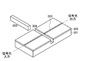
- a ⁇ / 2 wavelength plate 305 is inserted into the groove 304 formed in the Si substrate 301 and the optical circuit 302 thereon.
- the optical circuit 302 is composed of a quartz optical waveguide 303.
- the groove 304 is formed from the optical circuit 302 to a part of the Si substrate 301, and extends in a direction orthogonal to the waveguide direction of the optical waveguide 303.
- the groove 304 is, for example, 20 ⁇ m wide and 150 ⁇ m to 200 ⁇ m deep.
- the ⁇ / 2 wave plate 305 is formed of, for example, a stretched polyimide film. Since the birefringence of the stretched polyimide film is about 0.05, the stretched polyimide film functions as a ⁇ / 2 wave plate when the thickness of the stretched polyimide film is about 15 ⁇ m in the communication wavelength band of 1.5 ⁇ m. ..
- the transmission optical characteristic may have polarization dependency. As described above, by inserting the ⁇ / 2 wavelength plate 305 into the groove 304, it becomes possible to compensate for the polarization dependence of the transmission optical characteristic of the optical waveguide 303 (see Patent Document 1).
- Polyimide stretched film has a certain polarization direction. Therefore, in an optical waveguide array in which multiple optical waveguides are formed on a substrate, in order to insert wave plates with different polarization directions into adjacent optical waveguides, insert wave plates with different polarization directions into each optical waveguide. Will be done.
- the polarization beam splitter 400 can be configured as shown in FIG. 12 by using two wave plates each having a different polarization direction.
- the polarization beam splitter 400 is a waveguide type polarization beam splitter, and is formed on a substrate 401, an input optical waveguide 402, a Y branch coupler 403 optically connected to the input optical waveguide 402, and a Y branch coupler 403.
- the polarization beam splitter 400 includes a 2 ⁇ 2 MMI (Multi mode interference) 406 formed on the substrate 401 and connected to the TE polarization waveguide 404 and the TM polarization waveguide 405, and outputs to the 2 ⁇ 2 MMI 406, respectively.
- a TE polarized light output optical waveguide 407 and a TM polarized light output optical waveguide 408 are connected to each other.
- the TE polarization waveguide 404 and the TM polarization waveguide 405 are crossed so as to cross the TE polarization waveguide 404 and the TM polarization waveguide 405 in a direction orthogonal to the light guide direction.
- a groove 411 having a depth (specifically, a depth of 150 ⁇ m to 200 ⁇ m) is formed.
- the groove 411 is formed by dicing.
- a ⁇ / 4 wavelength plate (90 degrees) 412 is inserted so as to cross the TE polarization waveguide 404, and a ⁇ / 4 wavelength plate (0 degrees) 413 is inserted so as to cross the TM polarization waveguide 405. ing.
- a ⁇ / 4 wavelength plate 412 and a ⁇ / 4 wavelength plate 413 are inserted between a Y-branching coupler 403 and a 2 ⁇ 2 MMI 406, and a TM wave 90 And the TE wave is advanced by ⁇ 90 degrees by the ⁇ / 4 wave plate 413.
- the Y-branch coupler 403 By shifting the phases of the two lights split by the Y-branch coupler 403 by 90 ° between + and ⁇ and inputting them to the 2 ⁇ 2 MMI 406, only the TE polarized light is output from the TE polarized light output optical waveguide 407, and the TM polarized light output optical waveguide 408 is output. Outputs only TM polarized light (see Non-Patent Document 1).
- the above-mentioned waveguide type polarization beam splitter provides a polarization beam splitter with excellent temperature characteristics because the phase difference between polarized waves is added by the wave plates inserted in both arms.
- the wavelength plate there is a circuit having a wavelength multiplexing / demultiplexing function by inserting a wavelength filter, which is used for wavelength multiplexing transmission and the like (see Patent Document 2).
- the width of the groove in which the optical circuit is formed for disposing the optical element is made larger than the thickness of the optical element. This is because it is very difficult to form a groove that matches the thickness of the optical element and to dispose the optical element in this groove, because it requires high accuracy. If the width of the groove is made larger than the thickness of the optical element, the groove can be easily formed and the optical element can be easily arranged in the groove.
- a groove 503 extending in a direction perpendicular to the waveguide direction of the optical waveguide 502 and crossing the optical waveguide 502 is formed in the substrate 501 and the optical circuit including the optical waveguide 502.
- a plate-shaped optical element 504 is arranged in the groove 503.
- an optical element 504 composed of a polyimide wave plate, which is relatively frequently used has a thickness of 15 ⁇ m, and the width of the groove 503 in which this is arranged is set to about 20 ⁇ m, which is larger than the thickness of the optical element 504. Therefore, a gap of, for example, 5 ⁇ m is formed between the side surface of the groove 503 and the optical element 504.
- the groove 503 portion does not have an optical waveguide structure, for example, the light 511 guided through the optical waveguide 502 and emitted from the light emitting end face on the side surface of the groove 503 is accompanied by the diffraction spread and the groove 503. Propagation loss occurs because it propagates across. This loss is larger than the loss considering the thickness of the optical element 504. Further, when the light 511 propagating through the space of the gap enters the optical element 504, a loss due to Fresnel reflection also occurs.
- the above-mentioned gap is filled with a refractive index matching material 505 having a higher refractive index than the core 502a of the optical waveguide 502 and the optical element 504. It has a connection structure.
- the refractive index matching material 505 By filling the gap between the side surface of the groove 503 and the optical element 504 with the refractive index matching material 505, the diffraction spread of the light 511 can be suppressed to some extent, and the loss can be reduced.
- optical integrated circuit can be made smaller by applying the above-mentioned optical element to this optical circuit.
- the polarization beam splitter can be made smaller by combining the above optical circuit with two wave plates each having a different polarization direction as an optical element.
- the spot size converter itself is often large in size to convert the mode field diameter to low loss, it is not possible to take full advantage of the above-mentioned miniaturization. Further, since it is necessary to dispose the optical element at a position where the mode field diameter is enlarged to a desired value by the spot size converter, the groove forming accuracy is required, and the difficulty of mounting the optical element is increased. There are some drawbacks.
- the present invention has been made to solve the above problems, and an optical element is arranged in the middle of an optical waveguide in an optical circuit without increasing the difficulty of mounting the optical element on the optical circuit.
- the optical connection structure according to the present invention includes a first optical waveguide having a first light incident / exiting end surface formed on one end side and a first optical waveguide that is formed on one end side and faces the first light incident / exiting end surface of the first optical waveguide.
- a second optical waveguide having two light entering / exiting end faces, an optical element arranged between the first light entering / exiting end face and the light entering / exiting end face, a space between the first light entering / exiting end face and the optical element, and And a condenser lens disposed at least on one side between the two light entrance / exit end surfaces and the optical element, wherein the condenser lens is on an optical axis connecting the first light entrance / exit end surface and the second light entrance / exit end surface. It is arranged.
- At least one of a space between the first light entrance / exit end face and the optical element and a part between the second light entrance / exit end face and the optical element are filled, and Has a resin layer having a different refractive index, and the condenser lens is formed by being embedded in the resin layer.
- a substrate on which a first optical waveguide and a second optical waveguide are formed on one surface thereof, and a support portion formed on the substrate and supporting a condenser lens are further provided.
- the condenser lens is made of photo-cured resin.
- a resin layer is provided which fills at least one of the space between the first light entrance / exit end face and the optical element and the part between the second light entrance / exit end face and the optical element.
- the resin layer further defines a space and faces a main convex surface on the optical axis, and defines a sub-convex surface that is convex toward the main convex surface.
- the resin layer is made of a photocured resin.
- the first optical waveguide and the second optical waveguide are composed of optical waveguides formed in the same layer and are arranged with a gap formed in the optical waveguides interposed therebetween, , Placed in the gap.
- the condensing lens is arranged between at least one of the first light entrance / exit end face and the optical element and between the second light entrance / exit end face and the optical element, without increasing the difficulty of mounting the optical element on the optical circuit, the optical element is placed in the optical waveguide in the optical circuit and the propagation loss caused by placing the optical element in the optical waveguide is suppressed. The excellent effect of being able to be obtained is obtained.
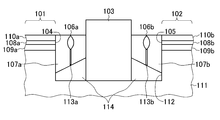
- FIG. 1 is a sectional view showing the configuration of the optical connection structure according to the first embodiment of the present invention.
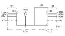
- FIG. 2 is a sectional view showing the configuration of another optical connection structure according to the first embodiment of the present invention.
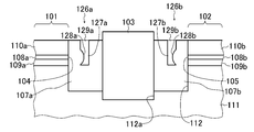
- FIG. 3 is a sectional view showing the configuration of the optical connection structure according to the second embodiment of the present invention.
- FIG. 4 is a sectional view showing the configuration of another optical connection structure according to the second embodiment of the present invention.
- FIG. 5 is a sectional view showing the configuration of another optical connection structure according to the second embodiment of the present invention.
- FIG. 6 is a sectional view showing the structure of the optical connection structure according to the third embodiment of the present invention.
- FIG. 7 is a sectional view showing the configuration of another optical connection structure according to the third embodiment of the present invention.
- FIG. 1 is a sectional view showing the configuration of the optical connection structure according to the first embodiment of the present invention.
- FIG. 2 is a sectional view showing the configuration of another optical connection structure according to the first embodiment
- FIG. 8 is a sectional view showing the configuration of another optical connection structure according to the third embodiment of the present invention.
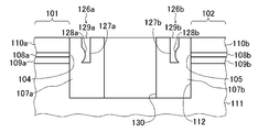
- FIG. 9 is a sectional view showing a partial configuration of another optical connection structure according to the third embodiment of the present invention.
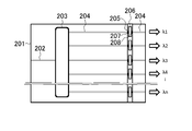
- FIG. 10 is a configuration diagram showing a configuration example of an optical circuit as an application example of the optical connection structure in the present invention.
- FIG. 11 is a perspective view showing a conventional optical connection structure.
- FIG. 12 is a plan view showing an example of an optical circuit using a wave plate.
- FIG. 13 is a sectional view showing a conventional optical connection structure.
- optical connection structure according to the embodiment of the present invention will be described below.
- This optical connection structure includes a first optical waveguide 101, a second optical waveguide 102, and an optical element 103.
- the first optical waveguide 101 has a first light input / output end face 104 formed on one end side.
- the first light entrance / exit end surface 104 is a boundary surface between the inside and the outside of the first optical waveguide 101 on one end side of the first optical waveguide 101.
- the light guided from the other end of the first optical waveguide 101 is emitted to the outside from the first light entrance / exit end face 104.
- the second optical waveguide 102 has a second light incident / exiting end surface 105 formed on one end side and facing the first light incident / ejecting end surface of the first optical waveguide.
- the second light entrance / exit end surface 105 is a boundary surface between the inside and the outside of the second optical waveguide 102 on one end side of the second optical waveguide 102.
- the light guided from the other end of the second optical waveguide 102 is emitted to the outside from the second light entrance / exit end face 105.
- the first optical waveguide 101 is composed of a first core 108a, a first lower clad 109a, and a first upper clad 110a.
- the second optical waveguide 102 is composed of a second core 108b, a second lower clad 109b, and a second upper clad 110b. Further, the first optical waveguide 101 and the second optical waveguide 102 are formed on the substrate 111.
- the first optical waveguide 101 and the second optical waveguide 102 are formed by dividing one optical waveguide formed in the same layer on the substrate 111 by the groove (gap) 112.
- the groove 112 is formed in the substrate 111 by dividing the optical waveguide perpendicularly to the waveguide direction of the optical waveguide. Further, the grooves 112 are formed such that the opposite side surfaces are parallel to each other.
- the first light entering / exiting end surface 104 and the second light entering / exiting end surface 105 are arranged so as to face each other on two opposite side surfaces of the groove 112 formed in the substrate 111. Further, the optical axis of the outgoing light emitted from the first light entrance / exit end face 104 and the optical axis of the outgoing light exiting from the second light entrance / exit end face 105 are arranged on the same line.
- the first condensing lens 106a arranged between the first light input / output end face 104 and the optical element 103, the second light input / output end face 105, and the optical element 103 are provided.
- the first condenser lens 106a and the second condenser lens 106b are arranged on the optical axis connecting the first light incident / exiting end surface 104 and the second light incident / exiting end surface 105.
- the first condenser lens 106a and the second condenser lens 106b have a so-called convex lens shape.
- the 1st condensing lens 106a and the 2nd condensing lens 106b can be comprised from the resin hardened
- the first resin layer 107a filling the space between the first light entrance / exit end face 104 and the optical element 103, and the part between the second light entrance / exit end face 105 and the optical element 103.
- a second resin layer 107b for filling The first condenser lens 106a is formed by being embedded in the first resin layer 107a, and the second condenser lens 106b is formed by being embedded in the second resin layer 107b.
- the first resin layer 107a is made of a material having a refractive index different from that of the first condenser lens 106a.
- the second resin layer 107b is made of a material having a refractive index different from that of the second condenser lens 106b.
- the first resin layer 107a is made of a material having a lower refractive index than the first condenser lens 106a.
- the second resin layer 107b is made of a material having a lower refractive index than the second condenser lens 106b.
- the first condenser lens 106a and the second condenser lens 106b are so-called convex lenses.
- the first resin layer 107a and the second resin layer 107b can be made of a photo-cured resin.
- the optical element 103 is a plate-shaped element, for example, a ⁇ / 2 wavelength plate.
- the optical element 103 can also be a wavelength filter. If the optical element 103 is a wavelength filter, it can split light of 1.3 ⁇ m and light of 1.5 ⁇ m by an optical connection structure.
- the light guided through the first optical waveguide 101 and emitted from the first light entrance / exit end face 104 propagates through the first resin layer 107a toward the optical element 103 with diffraction spread. ..
- the light propagating through the first resin layer 107a with the diffraction spread is condensed by the first condenser lens 106a, and the diffraction spread is suppressed.
- the light passing through the first condenser lens 106a enters the optical element 103 with its propagation loss suppressed.
- the light guided through the first optical waveguide 101 emitted from the first light entrance / exit end surface 104, enters the optical element 103, and exits from the optical element 103 also accompanies the diffraction broadening, and the second light entrance / exit end surface. It propagates toward the second resin layer 107 b toward 105.
- the light propagating through the second resin layer 107b with the diffraction spread is condensed by the second condenser lens 106b, and the diffraction spread is suppressed.
- the light passing through the second condenser lens 106b is suppressed in propagation loss and enters the first optical waveguide 101 through the second light entrance / exit end face 105.
- the first condensing lens 106a is arranged between the first light entrance / exit end face 104 and the optical element 103, and the second light entrance / exit end face 105 and the optical element are arranged. Since the second condenser lens 106b is arranged between the optical element 103 and the optical element 103, the optical element 103 can be arranged in the optical waveguide in the optical circuit while suppressing the propagation loss.
- the shape and materials of the first condenser lens 106a and the second condenser lens 106b are appropriately selected so that the focal length can obtain the highest effect of suppressing the propagation loss in accordance with the groove width of the groove 112. Set.
- the shape of the lens can be spherical or uneven.
- the lens may be a cylindrical lens, or may be a photonic crystal using a photocurable resin or a metasurface (see Non-Patent Document 6).
- the first condensing lens 106a and the second condensing lens 106b may be any lens configuration capable of condensing light or collimating the light to reduce excess loss due to diffraction spread.
- the optical element 103 is in contact with the bottom of the groove 112.
- the present invention is not limited to this, and the optical element 103 is separated from the bottom of the groove 112 as shown in FIG.
- the optical element 103 may be arranged by using the above.
- the first light entrance / exit end face 104 and the optical element 103 and the second light entrance / exit end face 105 and the optical element 103 are interposed between the bottom of the groove 112 and the lower surface of the optical element 103.
- the resin layer 107 may be filled with the resin layer 107 integrally formed.
- This optical connection structure further includes a first support part 113a and a second support part 113b in addition to the optical connection structure of the first embodiment described above.
- the first support portion 113a is formed on the bottom surface of the groove 112 of the substrate 111 and supports the first condenser lens 106a.
- the second support portion 113b is formed on the bottom surface of the groove 112 of the substrate 111 and supports the second condenser lens 106b.
- the first support portion 113a and the second support portion 113b are used in the manufacturing process of the first condenser lens 106a and the second condenser lens 106b of the optical connection structure described later.
- the groove 112a is further formed in the center of the groove 112, and the bottom of the optical element 103 is fitted in the groove 112a.
- the groove 112a is used for stably disposing the optical element 103 in the groove 112 during the manufacturing of an optical connection structure described later.
- the optical 3D modeling technology is a technology in which a photocurable resin is locally photocured by irradiating a focused laser beam, and a structure such as a lens or an optical waveguide is three-dimensionally manufactured by the photocured resin. Is.
- the lens can be formed at the place where the lens is placed. Therefore, compared to a manufacturing method in which a separately formed lens is incorporated later, active alignment is not required, and the trouble of assembling the lens in a minute portion and the damage around the assembling portion that occurs when assembling are avoided. There is an advantage that you can.
- the active alignment for example, light is incident on the first optical waveguide 101, the light is propagated between the first light entrance / exit end face 104 and the second light entrance / exit end face 105, and output from the second optical waveguide 102. This is a positioning technique that determines the component position between the first light entrance / exit end face 104 and the second light entrance / exit end face 105 by observing the change in the intensity of the generated light.
- the photo-curable resin When two-photon absorption is used, the photo-curable resin can be cured by light having a relatively long wavelength that is transmitted (not absorbed) through the photo-curable resin for forming the lens. Photocuring can be suppressed in areas other than the location. Further, since the light output required for photocuring due to two-photon absorption is about several mW, it is sufficient, and therefore it is easy to fabricate a lens structure without optical damage. Further, the optical 3D modeling apparatus currently on the market has a very small structure resolution of 1 ⁇ m or less, and is used for forming the micro optical system disclosed in Non-Patent Document 7, which is a very small area. It is possible to make a very small lens.
- the groove 112 is formed on the substrate 111 by dicing or etching. After forming the groove 112, a groove 112a is further formed. The groove 112a is formed to prevent the plate-shaped optical element 103 from collapsing, as described below.
- the optical element 103 may fall down. As described later, the first condenser lens 106a and the second condenser lens 106b are formed between the groove 112 and the optical element 103, and then the first resin layer 107a and the second resin layer 107b are formed. If the optical element 103 is tilted before forming the first resin layer 107a and the second resin layer 107b, the first condenser lens 106a and the second condenser lens 106b may be damaged. On the other hand, if the groove 112a is formed and the bottom of the optical element 103 is fitted into the groove 112a, the optical element 103 can be prevented from falling.
- the optical element 103 can be supported by using a jig or the like on the optical waveguide layer on which the first optical waveguide 101 and the second optical waveguide 102 are formed.
- the jig is removed after forming the first condenser lens 106a and the second condenser lens 106b, forming the first resin layer 107a and the second resin layer 107b.
- the photo-curable resin liquid used for optical 3D modeling is introduced into the groove 112 in which the optical element 103 is arranged, in other words, in the region where the first resin layer 107a and the second resin layer 107b are formed.
- the photocurable resin for example, an acrylic resin can be used.
- alignment marks for determining the positions where the first condenser lens 106a and the second condenser lens 106b are formed are formed in advance on the upper surfaces of the first optical waveguide 101 and the second optical waveguide 102, for example. Keep it.
- the plane of the substrate 111 is based on the alignment mark.
- the formation location of the first condenser lens 106a in the direction can be determined.
- the alignment mark is formed on the upper surfaces of the first optical waveguide 101 and the second optical waveguide 102 by a well-known photolithography technique and etching technique.
- the location of the first condensing lens 106a and the second condensing lens 106b can also be determined by using the interface detection function of the optical 3D modeling apparatus that performs optical 3D modeling.
- the optical 3D modeling apparatus generally has a function of measuring a difference in refractive index to detect an interface, and determining a position to be irradiated with exposure light with reference to the detected position of the interface.
- the position of the bottom surface of the groove 112 and the position of the upper surface of the first optical waveguide 101 can be detected by the interface detection function described above. Since the thickness of the first lower cladding 109a of the first optical waveguide 101, the cross-sectional dimension (diameter) of the first core 108a, and the like are known, the first light incident / emission end surface 104 is determined from the detected bottom surface position of the groove 112. The position of the optical axis of the emitted light that is emitted further in the depth direction of the groove 112 can be determined.
- the first condensing lens 106a is arranged on the optical axis of the emitted light emitted from the first light incident / emission end face 104, if the position of the groove 112 of the optical axis in the depth direction is known, the first condensing lens 106a in the depth direction is formed. The formation position of the condenser lens 106a can be determined.
- the interface positions of the first lower clad 109a, the second lower clad 109b, and the first core 108a can be determined in the plane direction of the substrate 111 due to the difference in refractive index between the first clad and the first core 108a. ..
- the formation position of the first condenser lens 106a in the plane direction of the substrate 111 can also be determined by using the interface position in the plane direction of the substrate 111 as a reference.
- the photo-curable resin liquid filled between the optical element 103 and the side surface of the groove 112 is removed.
- the position of the determined coordinates is irradiated with light to form the first condenser lens 106a and the second condenser lens 106b.
- a predetermined structure is gradually formed in one direction, for example, from the bottom surface side of the groove 112 to the upper side.
- the first condensing lens 106a and the second condensing lens 106b are formed by optical 3D
- the first condensing lens 106a and the second condensing lens 106b formed by optical 3D float in the photocurable resin liquid. It will be in the state of being. Since the photo-cured first condensing lens 106a and second condensing lens 106b have a higher density than the uncured photo-curable resin liquid, they settle in the photo-curable resin liquid and deviate from predetermined positions. become.
- the first support portion 113a and the second support portion 113b are formed first, and then the first condenser lens 106a, The second condenser lens 106b is formed.
- the condenser lens 106a and the second condenser lens 106b can be fixed at designed positions (coordinates).
- the fixing portion 114 that fixes the optical element 103 at the bottom of the groove 112 is formed. It can also be formed.
- photocuring the photocurable resin liquid by optical 3D modeling to form the fixing portion 114 it is possible to prevent the optical element 103 from falling when removing an uncured photocurable resin liquid described later. .. Further, when forming the fixing portion 114, it is not necessary to provide the groove 112a described with reference to FIG.
- the exposure light is emitted from above the substrate 111 to the bottom of the groove 112.
- the light is condensed at the lens forming position, and therefore, the beam diameter of the light is larger before this. Therefore, a part of the light for exposure may be applied by the upper end portion of the optical element 103 located above the focus position. Since the surroundings of the optical element 103 are air and there is a difference in refractive index between the optical element 103 and the surrounding air, as described above, a part of the light for exposure is partially transmitted along the optical path. If it reaches the upper end of the, the shadowing where the converging point shifts may occur.
- This problem is caused, for example, by using resin having a refractive index equal to that of the optical element 103 or a refractive index matching material for the portion of the optical element 103 protruding above the inside of the groove 112, so that the exposure light passes therethrough. This is solved by eliminating the part where the difference in refractive index occurs in the entire area of the optical path.
- an uncured photocurable resin liquid is used using a solvent such as ethanol. Are dissolved and removed.
- a predetermined resin liquid is supplied and filled between the side surface of the groove 112 and the optical element 103 on which the second support portion 113b, the first condenser lens 106a, and the second condenser lens 106b are formed,
- the first resin layer 107a and the second resin layer 107b are formed by curing the filled resin liquid.
- This resin liquid can be composed of, for example, a photocurable resin. Further, this resin liquid may be composed of a thermosetting resin.
- the width of the groove 112 was 100 ⁇ m, and a polyimide wave plate having a thickness of 15 ⁇ m was used as an optical element.
- the first optical waveguide 101 and the second optical waveguide 102 are silica optical waveguides having a relative refractive index difference of 1.5% between the core and the clad, and light having a wavelength of 1.55 ⁇ m is used.
- the space between the optical element 103 and the side surface of the groove 112 is filled with a refractive index manufacturing agent. With the conventional structure, a loss of about 3 dB occurs, but according to the second embodiment, the excess loss can be reduced to about 0.5 dB.
- a first condenser lens 106a is formed between the first optical waveguide 101 and the optical element 103, and the optical element 103 and the second optical waveguide 102 are provided on the second optical waveguide 102 side. It is also possible to make it in contact with the input / output end face 105. In this case, the second condenser lens 106b and the second resin layer 107b described with reference to FIGS. 1 and 3 are not formed.
- a second condenser lens 106b is formed between the second optical waveguide 102 and the optical element 103, and the optical element 103 and the first light input / output end face 104 are in contact with each other on the first optical waveguide 101 side. It can also be in a state.
- the optical element 103 when the optical element 103 is introduced into the groove 112 in the manufacturing process of the optical connection structure, the optical element 103 can be placed in contact with either side surface of the groove 112. It becomes possible to prevent the optical element 103 from collapsing within 112.
- This optical connection structure has a first space including the first condenser lens 106a and the second condenser lens 106b of the optical connection structure of the first embodiment described above inside the first resin layer 107a and the second resin layer 107b.
- 127a and a second space 127b are defined as a first condensing lens 126a and a second condensing lens 126b formed by a first main convex surface 128a and a second main convex surface 128b that are convex toward the optical element 103 side.
- the first space 127a and the second space 127b are arranged on the optical axis connecting the first light entrance / exit end face 104 and the second light entrance / exit end face 105.
- the functions of the first condenser lens 126a and the second condenser lens 126b are expressed by the first main convex surface 128a and the second main convex surface 128b that define the first space 127a and the second space 127b.
- the first space 127a and the second space 127b have a substantially rectangular parallelepiped whose opposing two surfaces are parallel to the side surfaces of the groove 112 as a basic shape, and the surfaces facing the optical element 103 side of this rectangular parallelepiped shape. It has a shape in which a first main convex surface 128a and a second main convex surface 128b are formed.
- the photo-curable resin liquid is introduced into the regions where the first resin layer 107a and the second resin layer 107b are formed, and the introduced photo-curable resin liquid except the first space 127a and the second space 127b.
- the first condenser lens 126a and the second condenser lens 126b can be formed. Curing of the region other than the first space 127a and the second space 127b of the photocurable resin liquid may be performed by the above-described optical 3D modeling technique.
- the first space 127a and the second space 127b are provided with a first opening 129a and a second opening 129b that communicate with the upper surfaces of the first resin layer 107a and the second resin layer 107b, respectively.
- the uncured region can be removed through the first opening 129a and the second opening 129b.
- the optics are formed in the groove 112. The fall of the element 103 does not damage the first condenser lens 126a and the second condenser lens 126b.
- the photo-curable resin liquid By the way, it may be difficult to sufficiently photo-cure the photo-curable resin liquid by the optical 3D modeling technique, for example, in the vicinity of the side surface of the groove 112 due to the influence of the shadowing described above.
- the area that cannot be sufficiently photo-cured by the optical 3D modeling technique is separately irradiated with exposure light (ultraviolet light) to be photo-cured.
- exposure light ultraviolet light
- the photocurable resin liquid can accelerate the curing by heat, it is possible to completely cure the region that cannot be sufficiently photocured by the optical 3D modeling technique by heating.
- the first resin layer 107a and the second resin layer 107b other than the first space 127a and the second space 127b which are the first condenser lens 126a and the second condenser lens 126b are cured.
- the photocurable resin liquid is again introduced into the first space 127a and the second space 127b that have been formed once, and the first main convex surface 128a and the second main convex surface 128b are again formed by the photocurable resin liquid. It is easy to adjust the shape. By adjusting the shapes of the first main convex surface 128a and the second main convex surface 128b, it is possible to adjust the effect of reducing excess loss due to diffraction spread.
- Such shape adjustment of the first main convex surface 128a and the second main convex surface 128b is performed by, for example, guiding the light from the first optical waveguide 101 side to the second optical waveguide 102 side and emitting the second optical waveguide 102 from the output side. It may be performed while observing the intensity change of the light output from. The state in which the intensity of the observed light is the highest is the optimum shape of the first main convex surface 128a and the second main convex surface 128b which are the first condenser lens 126a and the second condenser lens 126b.
- the resin when the resin is cured to form the first resin layer 107a and the second resin layer 107b, there is a deviation in shape from the design value due to shrinkage during curing, and unevenness of the cured resin. It is possible to correct the deviation of the shape from the design value due to it later. Therefore, according to the third embodiment, it is possible to improve the manufacturing yield of the optical connection structure.
- a first condenser lens 126a ′ is formed between the first optical waveguide 101 and the optical element 103, and the optical element 103 and the second optical waveguide 103 are provided on the second optical waveguide 102 side. It is also possible to make it in contact with the light entrance / exit end face 105.
- the second condenser lens 126b and the second resin layer 107b described with reference to FIG. 6 are not formed.
- the first resin layer 107a defines the first space 127a, faces the first main convex surface 128a on the optical axis, and is convex toward the first main convex surface 128a. 128a 'may be defined.
- the first condensing lens 126a and the second collecting lens 126a are provided with a fitting groove 130 for arranging the optical element 103 between the first resin layer 107a and the second resin layer 107b.
- the optical element 103 may be inserted into the fitting groove 130 after forming the first space 127a and the second space 127b to be the optical lens 126b.
- On the side surfaces of the first resin layer 107a and the second resin layer 107b that form the fitting groove 130 if the curing is insufficient, this portion can be elastically deformed and the optical element 103 can be easily inserted. is there. After inserting the optical element 103, the insufficiently cured region is completely cured.
- a space is formed inside a resin layer filling at least one of the first light entrance / exit end face and the optical element and between the second light entrance / exit end face and the optical element, and used as a condenser lens
- a material liquid, resin
- the condenser lens is filled with the material filling the space.
- the space is defined by a main convex surface that is convex toward the optical element side, a material having a lower refractive index than resin is filled.
- the space when the space is filled with a resin having a refractive index higher than that of the resin layer, the space is defined by a concave surface concave on the optical element side.
- the obtained condenser lens is the same as the condenser lens described with reference to FIG.
- optical connection structure of the present invention can be applied to an optical circuit for wavelength division multiplexing communication in which circuits integrated with wavelength filters are arrayed.
- this optical circuit light input to the input optical waveguide 202 formed on the substrate 201 is branched by the optical splitter 203 into a plurality of optical waveguides 204.
- a groove 205 extending perpendicularly to the waveguiding direction of the optical waveguide 204 is formed at a predetermined position of the substrate 201.
- the plurality of optical waveguides 204 are divided by the groove 205.
- the groove 205 is provided with a wavelength filter 206 corresponding to each of the plurality of optical waveguides 204. Further, in the groove 205, a first optical waveguide 207 and a second optical waveguide 208 are formed between the wavelength filter 206 and each side surface of the groove 205. The light input / output end faces of the first optical waveguide 207 and the second optical waveguide 208 on the wavelength filter 206 side are in contact with the first optical waveguide 207.
- a comb-shaped wave plate in which the delay given by the wave plate changes periodically in the plate longitudinal direction can be applied.
- a magneto-optical material can be applied as the optical element.
- An optical circuit such as an optical isolator can be realized by using the magneto-optical material as an optical element.
- the condensing lens is arranged at least between the first light entrance / exit end face and the optical element and between the second light entrance / exit end face and the optical element.
- the optical element is placed in the middle of the optical waveguide in the optical circuit without increasing the difficulty of mounting the optical element in the optical circuit, and the propagation loss caused by placing the optical element in the middle of the optical waveguide is suppressed. become able to.
Landscapes
- Physics & Mathematics (AREA)
- General Physics & Mathematics (AREA)
- Optics & Photonics (AREA)
- Optical Integrated Circuits (AREA)
- Optical Couplings Of Light Guides (AREA)
Abstract
第1光入出射端(104)と光学素子(103)との間に配置された第1集光レンズ(106a)と、第2光入出射端(105)と光学素子(103)との間に配置された第2集光レンズ(106b)とを備える。第1集光レンズ(106a)および第2集光レンズ(106b)は、第1光入出射端(104)と第2光入出射端(105)とを結ぶ光軸上に配置されている。
Description
本発明は、光接続構造に関し、より具体的には、光学素子が集積された光接続構造に関する。
大容量の光情報を高速、低コストに伝送、処理するためには、光回路における光デバイスの集積化が必要不可欠である。光回路は、基板表面に屈折率の高い部分からなるコアと、コアより屈折率の低いクラッドとからなる光導波路で、複数の光デバイスを接続したものである。この光回路に光デバイスを集積化した光集積回路には、さまざまなデバイスを組み込むことが可能である。
光回路の材料としてはポリマー、石英ガラス、化合物半導体、Si、ニオブ酸リチウムなどの強誘電体がある。また、光回路を構成する光導波路には、石英ガラス基板またはシリコン基板上に、石英系ガラスを主たる材料として作製される石英系光導波路があり、主として通信分野において実用に供せられている。石英系光回路上の石英系光導波路は、伝播損失が低い、信頼性・化学的安定性が高い、および加工性がよいなどの特徴を有している。また、石英系光ファイバとの整合性がよいため、標準的な通信用石英系光ファイバと接続した場合においても、低損失・高信頼性を有している。
現在、石英系光導波路により構成したY分岐パワースプリッタ、マッハ・ツェンダ干渉計(MZI:Mach-Zehnder Interferometer)、MZIを利用した光スイッチ、およびアレイ導波路型波長合分波器(AWG:Arrayed Waveguide Grating)などの光回路(PLC:Planar Lightwave Circuits)の開発が進められている。これらの光回路は、近年、構築が進められつつある波長分割多重(WDM)光伝送システムを基盤とした、フォトニックネットワークシステムの重要なキーデバイスとなっている(非特許文献1、非特許文献2、非特許文献3参照)。
また、石英系光回路以外にも、近年、Si、化合物半導体、強誘電体材料などを用いて、より小型な光回路の開発が進んでいる。光回路に機能性を付与するために、光回路内に溝を設け、設けた溝に薄膜形状の光学素子を挿入する技術がしばしば用いられる。例えば、光回路内の導波光の偏波を制御するために、光導波路が形成された光回路に溝を設け、この溝に所望の位相差を与える波長板を挿入する方法がしばしば用いられる。
例えば、図11に示すように、Si基板301およびこの上の光回路302に形成された溝304に、λ/2波長板305を挿入する。光回路302は石英系の光導波路303から構成されている。溝304は、光回路302からSi基板301の一部にかけて形成され、光導波路303の導波方向と直交する方向に延在している。溝304は、例えば、幅20μm,深さ150μm~200μm程度とされている。このように形成された溝304に、光学素子であるλ/2波長板305を挿入することで、光回路302に機能性を付与する。
λ/2波長板305は、例えばポリイミド延伸フィルムにより形成される。ポリイミド延伸フィルムの複屈折率は約0.05であるため、通信波長帯である1.5μmの光においては、ポリイミド延伸フィルムは厚さ約15μmとすることにより、λ/2波長板として機能する。
Si基板301上の光導波路303は,複屈折を有するため,透過光学特性が偏波依存性を有することがある。上述したように、溝304にλ/2波長板305を挿入することにより、光導波路303の透過光学特性の偏波依存性を補償することが可能となる(特許文献1参照)。
ポリイミド延伸フィルムは一定の偏光方向を持つ。したがって、基板上に複数の光導波路が形成された光導波路アレイにおいて、隣接する光導波路に異なる偏光方向を持つ波長板を挿入するには、各光導波路に別々の偏光方向を有する波長板を挿入することになる。
例えば、各々異なる偏光方向を持つ2つの波長板を用いることで、図12に示すように、偏光ビームスプリッタ400を構成することができる。偏光ビームスプリッタ400は、導波路型偏光ビームスプリッタであり、基板401上に形成された、入力光導波路402と、入力光導波路402に光学的に接続されたY分岐カプラ403と、Y分岐カプラ403の出力にそれぞれ接続されたTE偏光導波路404およびTM偏光導波路405とを備える。また、偏光ビームスプリッタ400は、基板401上に形成された、TE偏光導波路404およびTM偏光導波路405に接続された2×2MMI(Multi mode interference)406を備え、2×2MMI406の出力にそれぞれが接続されたTE偏光出力光導波路407およびTM偏光出力光導波路408を備える。
偏光ビームスプリッタ400の上面には、TE偏光導波路404およびTM偏光導波路405を横切るように、TE偏光導波路404およびTM偏光導波路405の光の導波方向と直交する方向に、一定の深さ(具体的には深さ150μm~200μm)の溝411が形成されている。溝411は、ダイシングにより形成される。溝411には、TE偏光導波路404を横切るようにλ/4波長板(90度)412が挿入され、TM偏光導波路405を横切るようにλ/4波長板(0度)413が挿入されている。
この偏光ビームスプリッタ400は、Y分岐カプラ403と2×2MMI406との間に、λ/4波長板412と、λ/4波長板413とを挿入し、λ/4波長板412によりTM波を90度進め、λ/4波長板413によりTE波を-90度進める。Y分岐カプラ403によって分けられた2つの光の位相を+と-に90°シフトさせて2×2MMI406に入力することにより、TE偏光出力光導波路407からはTE偏光のみ、TM偏光出力光導波路408からはTM偏光のみが出力される(非特許文献1参照)。
上述した導波路型偏光ビームスプリッタは、偏波間の位相差を両アームに挿入された波長板によって付与するため、温度特性に優れた偏波ビームスプリッタを実現できる。波長板以外にも、波長フィルタを挿入することで波長合分波機能を持たせた回路なども存在し、波長多重伝送などに用いられている(特許文献2参照)。
Y. Hibino, "Arrayed-Waveguide-Grating Multi/Demultiplexers for Photonic Networks", IEEE CIRCUITS & DEVICES, pp. 21-27, 2000.
A. Himeno et al., "Silica-Based Planar Lightwave Circuits", IEEE Journal of Selected Topics in Quantum Electronics, vol. 4, no. 6, pp. 912-924, 1998.
M. ABE, "Silica-based waveguide devices for photonic networks", Journal of the Ceramic Society of Japan, vol. 116, no. 10, pp. 1063-1070, 2008.
M. Kawachi et al., "Silica waveguides on silicon and their application to integrated-optic components", Optical and Quantum Electronics, vol. 22, pp. 391-416, 1990.
Y. Nasu et al., "Temperature insensitive and ultra wideband silica-based dual polarization optical hybrid for coherent receiver with highly symmetrical interferometer design", Optics Express, vol. 19, no. 26, pp. B112-B118, 2011.
P. R. West et al., "All-dielectric subwavelength metasurface focusing lens", Optics Express, vol. 22, no. 21, pp. 26212-26221, 2014.
P.-I. Dietrich et al., "In situ 3D nanoprinting of free-form coupling elements for hybrid photonic integration", Nature Photonics, vol. 12, pp. 241-247, 2018.
ところで、前述したように、光学素子を配置するために光回路の形成された溝の幅は、光学素子の厚さより大きくされている。これは、光学素子の厚さと一致した溝を形成すること、およびこの溝に光学素子を配置することには、高い精度が要求され、非常に困難なためである。溝の幅を光学素子の厚さより大きくすれば、溝の形成が容易になり、溝に光学素子を配置することも容易となる。
例えば、図13に示すように、基板501と光導波路502を含む光回路とに、光導波路502の導波方向に垂直な方向に延在し、光導波路502を横断する溝503が形成されている。溝503に、板状の光学素子504が配置される。例えば、比較的よく用いられる、ポリイミド波長板より構成される光学素子504は、厚さが15μmであり、これを配置する溝503の幅は、光学素子504の厚さより大きい20μm程度としている。したがって、溝503の側面と光学素子504との間に、例えば、5μm分の隙間が形成される。
この場合、溝503の部分は、光導波路構造を有していないので、例えば、光導波路502を導波して溝503側面の光出射端面より出射した光511は、回折広がりを伴いながら溝503を横切るように伝播するので、伝播損失が発生する。この損失は、光学素子504の厚さを考慮した損失よりも大きい。また、隙間の空間を伝播する光511が光学素子504に入射するときに、フレネル反射による損失も発生する。
従来の技術では、上述した伝播損失およびフレネル反射による損失を低減する目的で、上述した隙間に、光導波路502のコア502aおよび光学素子504より高い屈折率を持つ屈折率整合材505を充填した光接続構造としている。溝503の側面と光学素子504との間の隙間に屈折率整合材505を充填することで、光511の回折広がりをある程度抑制することができ、損失を低減することが可能となる。
一方、近年、光回路のサイズ縮小によるコンパクトかつ高機能な光モジュール実現の目的から、コアとクラッドとの屈折率差が大きい光導波路による光回路が注目を集めている。コアとクラッドとの屈折率差が大きい光導波路は、光導波路の導波方向を変える光導波路の曲げの部分の曲率半径を小さくすることが可能であり、光回路をより小さくすることができるという利点がある。この光回路に前述した光学素子を適用することで、光集積回路をより小さくすることができる。例えば、上記光回路に、光学素子として各々異なる偏光方向を持つ2つの波長板を組み合わせることで、偏光ビームスプリッタをより小さくすることができる。
しかしながら、コアとクラッドとの屈折率差が大きい光導波路の場合、上述した溝側面の光導波路端から出射される光の広がり角がより大きな値をとるため、光学素子を配置した溝部における損失が、より大きくなるという欠点がある。コアとクラッドとの屈折率差が大きい光導波路の場合の損失の増大を抑制するために、溝の側面近くの光導波路に導波光のモードフィールド径を拡大するためのスポットサイズ変換器を導入し、モードフィールド径を拡大することによって、回折による損失を低減する技術が用いられる。
しかし、スポットサイズ変換器自体も低損失にモードフィールド径を変換するためには大きなサイズになることが多いため、前述した小型化のメリットを活かしきれない。また、スポットサイズ変換器によってモードフィールド径が所望の値まで拡大されている箇所に、光学素子を配置する必要があるため、溝の形成精度が必要とされ、光学素子の実装難易度が上昇することなどの欠点も発生する。
本発明は、以上のような問題点を解消するためになされたものであり、光回路に対する光学素子の実装の難易度を上げることなく、光回路の中の光導波路の途中に光学素子を配置するとともに、光導波路の途中に光学素子を配置することによって生じる伝播損失を抑制することを目的とする。
本発明に係る光接続構造は、一端側に形成された第1光入出射端面を有する第1光導波路と、一端側に形成されて、第1光導波路の第1光入出射端面と向かい合う第2光入出射端面を有する第2光導波路と、第1光入出射端面と光入出射端面との間に配置された光学素子と、第1光入出射端面と光学素子との間、および第2光入出射端面と光学素子との間の少なくとも一方に配置された集光レンズとを備え、集光レンズは、第1光入出射端面と第2光入出射端面とを結ぶ光軸上に配置されている。
上記光接続構造の一構成例において、第1光入出射端面と光学素子との間、および第2光入出射端面と光学素子との間の少なくとも一方を充填し、集光レンズの屈折率とは異なる屈折率を有する樹脂層を備え、集光レンズは樹脂層に埋め込まれて形成されている。
上記光接続構造の一構成例において、その一の面上に第1光導波路および第2光導波路が形成された基板と、基板の上に形成されて集光レンズを支持する支持部とをさらに備える。
上記接続構造の一構成例において、集光レンズは、光硬化した樹脂から構成されている。
上記光接続構造の一構成例において、第1光入出射端面と光学素子との間、および第2光入出射端面と光学素子との間の少なくとも一方を充填する樹脂層とを備え、樹脂層は、その内部に空間を含み、この空間を規定する、光学素子の側に凸とされた主凸面を有し、主凸面は、光軸の上に配置されて集光レンズの一部を構成する。
上記光接続構造の一構成例において、樹脂層は、さらに空間を規定するとともに、光軸の上で主凸面に向かい合い、主凸面に向かって凸とされた副凸面を規定する。
上記光接続構造の一構成例において、樹脂層は、光硬化した樹脂から構成されている。
上記光接続構造の一構成例において、第1光導波路および第2光導波路は、同一の層に形成された光導波路から構成されて光導波路に形成された隙間を挾んで配置され、光学素子は、隙間に配置されている。
以上説明したように、本発明によれば、第1光入出射端面と光学素子との間、および第2光入出射端面と光学素子との間の少なくとも一方に集光レンズを配置したので、光回路に対する光学素子の実装の難易度を上げることなく、光回路の中の光導波路の途中に光学素子を配置するとともに、光導波路の途中に光学素子を配置することによって生じる伝播損失を抑制することができるという優れた効果が得られる。
以下、本発明の実施の形態に係る光接続構造について説明する。
[実施の形態1]
はじめに、本発明の実施の形態1に係る光接続構造について、図1を参照して説明する。この光接続構造は、第1光導波路101と、第2光導波路102と、光学素子103とを備える。
はじめに、本発明の実施の形態1に係る光接続構造について、図1を参照して説明する。この光接続構造は、第1光導波路101と、第2光導波路102と、光学素子103とを備える。
第1光導波路101は、一端側に形成された第1光入出射端面104を有する。第1光入出射端面104は、第1光導波路101の一端側における第1光導波路101の内部と外部との境界面である。第1光導波路101の他端より導波してきた光は、第1光入出射端面104より外部に放射されることになる。また、第2光導波路102は、一端側に形成されて第1光導波路の第1光入出射端面と向かい合う第2光入出射端面105を有する。第2光入出射端面105は、第2光導波路102の一端側における第2光導波路102の内部と外部との境界面である。第2光導波路102の他端より導波してきた光は、第2光入出射端面105より外部に放射されることになる。
第1光導波路101は、第1コア108a、第1下部クラッド109a、および第1上部クラッド110aから構成されている。第2光導波路102は、第2コア108b、第2下部クラッド109b、および第2上部クラッド110bから構成されている。また、第1光導波路101、第2光導波路102は、基板111の上に形成されている。基板111の上の同一の層に形成されている1つの光導波路を、溝(隙間)112で分断することで、第1光導波路101および第2光導波路102が形成されている。溝112は、上記光導波路の導波方向に垂直にこの光導波路を分断して基板111に形成されている。また、溝112は、向かい合う側面が互いに平行に形成されている。
基板111に形成された溝112の向かい合う2つの側面で、第1光入出射端面104と第2光入出射端面105とが面と向かい合って配置される。また、第1光入出射端面104より出射する出射光の光軸と第2光入出射端面105より出射する出射光の光軸とは、同じ線の上に配置される。
また、実施の形態1の光接続構造は、第1光入出射端面104と光学素子103との間に配置された第1集光レンズ106aと、第2光入出射端面105と光学素子103との間に配置された第2集光レンズ106bとを備える。第1集光レンズ106aおよび第2集光レンズ106bは、第1光入出射端面104と第2光入出射端面105とを結ぶ光軸上に配置されている。第1集光レンズ106aおよび第2集光レンズ106bは、いわゆる凸レンズの形状とされている。第1集光レンズ106aおよび第2集光レンズ106bは、光硬化した樹脂から構成できる。
また、実施の形態1の光接続構造は、第1光入出射端面104と光学素子103との間を充填する第1樹脂層107aと、第2光入出射端面105と光学素子103との間を充填する第2樹脂層107bとを備える。第1集光レンズ106aは、第1樹脂層107aに埋め込まれて形成され、第2集光レンズ106bは、第2樹脂層107bに埋め込まれて形成されている。
第1樹脂層107aは、第1集光レンズ106aとは異なる屈折率の材料から構成されている。また、第2樹脂層107bは、第2集光レンズ106bとは異なる屈折率の材料から構成されている。実施の形態1では、第1樹脂層107aは、第1集光レンズ106aより屈折率が低い材料から構成されている。また、第2樹脂層107bは、第2集光レンズ106bより屈折率が低い材料から構成されている。この場合、第1集光レンズ106a、第2集光レンズ106bは、いわゆる凸レンズである。第1樹脂層107aおよび第2樹脂層107bは、光硬化した樹脂から構成できる。また、光学素子103は、板状の素子であり、例えば、λ/2波長板である。また、光学素子103は、波長フィルタとすることもできる。光学素子103は、波長フィルタとすれば、光接続構造により、例えば1.3μmの光と1.5μmの光を分波することができる。
実施の形態1によれば、第1光導波路101を導波して第1光入出射端面104より出射した光は、回折広がりを伴いながら光学素子103に向けて第1樹脂層107aを伝播する。この回折広がりを伴いながら第1樹脂層107aを伝播する光は、第1集光レンズ106aで集光され、回折広がりが抑制される。この結果、第1集光レンズ106aを通過した光は、伝播損失が抑制されて光学素子103に入射する。
また、第1光導波路101を導波して第1光入出射端面104より出射して光学素子103に入射し、光学素子103を出射した光も、回折広がりを伴いながら第2光入出射端面105に向けて第2樹脂層107bを伝播する。この回折広がりを伴いながら第2樹脂層107bを伝播する光は、第2集光レンズ106bで集光され、回折広がりが抑制される。この結果、第2集光レンズ106bを通過した光は、伝播損失が抑制されて第2光入出射端面105より第1光導波路101に入射する。
以上に説明したように、実施の形態1によれば、第1光入出射端面104と光学素子103との間に第1集光レンズ106aを配置し、第2光入出射端面105と光学素子103との間に第2集光レンズ106bを配置したので、光回路の中の光導波路途中に、伝播損失を抑制して光学素子103が配置できるようになる。
ところで、第1集光レンズ106a、第2集光レンズ106bは、溝112の溝幅に併せて伝播損失の最も高い抑制効果が得られる焦点距離となるように、形状や構成する材料を適宜に設定する。レンズの形状は、球状、凹凸形状とすることができる。また、レンズは、シリンドリカルレンズとしてもよく、光硬化性の樹脂を用いたフォトニック結晶やメタサーフェース(非特許文献6参照)でもよい。第1集光レンズ106a、第2集光レンズ106bは、光を集光、あるいは平行光にし、回折広がりによる過剰損失を減少させることが可能なレンズ構成であればよい。
ところで、図1を用いて説明した光接続構造では、溝112の底に光学素子103が接する状態としているが、これに限るものではなく、図2に示すように、溝112の底より離間して光学素子103を配置してもよい。この場合、第1光入出射端面104と光学素子103との間、および第2光入出射端面105と光学素子103との間を、溝112の底と光学素子103の下面との間を介して一体に形成された樹脂層107で充填する構成とすることができる。
[実施の形態2]
次に、本発明の実施の形態2に係る光接続構造について、図3を参照して説明する。この光接続構造は、前述した実施の形態1の光接続構造に、第1支持部113a,第2支持部113bをさらに備える。
次に、本発明の実施の形態2に係る光接続構造について、図3を参照して説明する。この光接続構造は、前述した実施の形態1の光接続構造に、第1支持部113a,第2支持部113bをさらに備える。
第1支持部113aは、基板111の溝112の底面上に形成され、第1集光レンズ106aを支持する。また、第2支持部113bは、基板111の溝112の底面上に形成され、第2集光レンズ106bを支持する。第1支持部113a、第2支持部113bは、後述する光接続構造の第1集光レンズ106a,第2集光レンズ106bの製造過程で用いられる。また、実施の形態2では、溝112の中央部に、さらに溝112aを形成し、溝112aに光学素子103の底部を嵌合させている。溝112aは、後述する光接続構造の製造の途中において、溝112の中に光学素子103を安定して配置するために用いる。
以下、実施の形態2における光接続構造の製造方法について説明する。光接続構造の製造方法はいくつか存在するが、1つの方法として2光子吸収を用いた光3D造形技術(非特許文献7参照)がある。光3D造形技術は、光硬化性の樹脂を、集光したレーザー光を照射することで局所的に光硬化させ、光硬化した樹脂でレンズや光導波路などの構造を3次元的に作製する技術である。
光3D造形技術によれば、レンズを配置する箇所でレンズが形成できる。このため、別途に形成したレンズを後から組み込む製造方法に比較し、アクティブアライメントなどを必要とせず、微細な箇所にレンズを組み込む手間や、組み込むときに発生する組み込み箇所周囲への損傷などが回避できるという利点がある。なお、アクティブアライメントは、例えば、第1光導波路101に光を入射し、第1光入出射端面104と第2光入出射端面105との間に光を伝搬させ、第2光導波路102から出力される光の強度変化を観察することで、第1光入出射端面104と第2光入出射端面105との間の部品位置を決定する位置合わせの技術である。
また、2光子吸収を用いた場合は、レンズを形成するための光硬化樹脂を透過する(吸収されない)比較的長い波長の光によって、光硬化樹脂を硬化させることが可能であり、レンズとする箇所以外の光硬化が抑制できる。また、2光子吸収による光硬化に必要な光の出力は数mW程度でも十分なため、光学的損傷を与えることなくレンズの構造を作製することも容易である。また、現在市販されている光3D造形装置は、作製できる構造の分解能が1μm以下と非常に小さく、非特許文献7に開示されている微小光学系の形成に用いられており、非常に小さい領域に微小なレンズを作製できる。
まず、基板111に、ダイシングやエッチングなどによって溝112を形成する。溝112を形成した後、さらに、溝112aを形成する。溝112aは、以下に説明するように、板状の光学素子103が倒れることを防ぐために形成する。
溝112に光学素子103を挿入し、第1樹脂層107a、第2樹脂層107bを形成していない段階では、光学素子103が倒れる可能性がある。後述するように、溝112と光学素子103との間に第1集光レンズ106a,第2集光レンズ106bを形成し、この後、第1樹脂層107a、第2樹脂層107bを形成する。第1樹脂層107a、第2樹脂層107bを形成する前に、光学素子103が倒れると、第1集光レンズ106a,第2集光レンズ106bを破損する可能性がある。これに対し、溝112aを形成し、溝112aに光学素子103の底部を嵌めておけば、光学素子103が倒れることが防止できるようになる。
また、第1光導波路101,第2光導波路102が形成されている光導波路層の上で、治具などを用いて光学素子103を支持しておくこともできる。治具は、第1集光レンズ106a,第2集光レンズ106bを形成し、第1樹脂層107a、第2樹脂層107bを形成した後で取り外す。
次に、光3D造形に用いる光硬化性樹脂液を、光学素子103を配置した溝112の内部、言い換えると、第1樹脂層107a、第2樹脂層107bを形成する領域に導入する。光硬化性樹脂は、例えば、アクリル系の樹脂を用いることができる。なお、予め、第1集光レンズ106a,第2集光レンズ106bを形成する箇所を決定するための、位置合わせマークを、例えば、第1光導波路101,第2光導波路102の上面に形成しておく。例えば、第1光導波路101の上面に形成した位置合わせマークと、第1集光レンズ106aの形成箇所との相対的な位置関係が既知であれば、位置合わせマークを基準に、基板111の平面方向における第1集光レンズ106aの形成箇所が決定できる。位置合わせマークは、よく知られたフォトリソグラフィ技術、およびエッチング技術により、第1光導波路101,第2光導波路102の上面に形成しておく。
また、第1集光レンズ106a,第2集光レンズ106bを形成する箇所の決定は、光3D造形を実施する光3D造形装置の界面検出機能を用いることでも実施できる。光3D造形装置は、一般に、屈折率の差を測定して界面を検出し、検出した界面の位置を基準として露光の光を照射する位置を決定する機能を備えている。
例えば、溝112の深さ方向において、溝112の底面の位置や、第1光導波路101の上面の位置が、上述した界面検出機能により検出できる。第1光導波路101の第1下部クラッド109aの厚さや、第1コア108aの断面の寸法(直径)などは既知であるため、検出した溝112の底面の位置より、第1光入出射端面104より出射する出射光の光軸の、溝112の深さ方向の位置が決定できる。第1集光レンズ106aは、第1光入出射端面104より出射する出射光の光軸上に配置するため、光軸の溝112の深さ方向の位置が分かれば、深さ方向における第1集光レンズ106aの形成位置が決定できる。
また、溝112の側面において、第1下部クラッド109a、第2下部クラッド109bと、第1コア108aとの間の屈折率差により、これらの界面位置が、基板111の平面方向の中で決定できる。基板111の平面方向における上記界面位置を基準とすることでも、基板111の平面方向における第1集光レンズ106aの形成箇所が決定できる。
上述したことにより、第1集光レンズ106a,第2集光レンズ106bを形成する座標を決定した後は、光学素子103と溝112の側面との間に充填されている光硬化性樹脂液の決定した座標の位置に光を照射し、第1集光レンズ106a,第2集光レンズ106bを形成する。光3D造形においては、一方向、例えば、溝112の底面の側から上方にかけて、徐々に所定の構造を形成する。このため、第1集光レンズ106a,第2集光レンズ106bを光3D造形すると、光3D造形した第1集光レンズ106a,第2集光レンズ106bが、光硬化性樹脂液の中に浮いている状態となる。光硬化した第1集光レンズ106a,第2集光レンズ106bは、未硬化の光硬化性樹脂液より密度が高いため、光硬化性樹脂液の中を沈降し、所定の形成箇所からずれることになる。
このため、第1集光レンズ106a,第2集光レンズ106bの光3D造形においては、第1支持部113a,第2支持部113bを先に形成し、この上に第1集光レンズ106a,第2集光レンズ106bを形成する。第1支持部113a,第2支持部113bを形成しておくことで、第1集光レンズ106a,第2集光レンズ106bが、光硬化性樹脂液の中で沈降することが防げ、第1集光レンズ106a,第2集光レンズ106bを、設計した位置(座標)に固定することができる。
なお、これらの光3D造形において、図4に示すように、第1支持部113a,第2支持部113bを形成するよりも前に、溝112の底部で光学素子103を固定する固定部114を形成することも可能である。光硬化性樹脂液を光3D造形により光硬化させて固定部114を形成しておくことで、後述する未硬化の光硬化性樹脂液を除去するときに、光学素子103が倒れることが防止できる。また、固定部114を形成する場合、図3を用いて説明した溝112aを備える必要は無い。
ところで、光3D造形により第1集光レンズ106a,第2集光レンズ106bを形成する場合、露光の光は、基板111の上方から溝112の底部への方向に照射することになる。光3D造形では、レンズ形成位置に光を集光させるため、これより手前では、光のビーム径がより大きい状態である。このため、集光位置より上側にある光学素子103の上端部により、露光のための光の一部がかかる場合がある。光学素子103の周囲は空気であり、光学素子103と周囲の空気との間には屈折率差があるため、上述したように露光のための光の一部が、光路の途中で光学素子103の上端部にかかると、集光点がずれるシャドウイングが発生する可能性がある。
この問題は、例えば、溝112の内部より上方に突出している光学素子103の部分を、光学素子103と同等の屈折率を持つ樹脂、もしくは屈折率整合材を用いることで、露光の光が通る光路上の全域で、屈折率差が発生する箇所を無くすことで解消する。次に、第1支持部113a,第2支持部113bおよび第1集光レンズ106a,第2集光レンズ106bを光3D造形した後、エタノールなどの溶剤を用い、未硬化の光硬化性樹脂液を溶解除去する。
次に、第2支持部113bおよび第1集光レンズ106a,第2集光レンズ106bが形成されている光学素子103と溝112の側面の間に、所定の樹脂液を供給して充填し、充填した樹脂液を硬化させることで、第1樹脂層107a、第2樹脂層107bを形成する。この樹脂液は、例えば、光硬化性の樹脂から構成することができる。また、この樹脂液は、熱硬化性の樹脂から構成することもできる。
上述した実施の形態2における光接続構造と、従来構造との比較を実施した結果について説明する。光接続構造は、溝112の幅を100μmとし、光学素子として厚さ15μmのポリイミド波長板を用いた。また、第1光導波路101、第2光導波路102は、コアとクラッドとの比屈折率差が1.5%の石英系光導波路とし、波長1.55ミクロンの光を用いた。従来の構造としては、光学素子103と溝112の側面の間を、屈折率製造剤で充填した。従来の構造では、約3dBの損失が発生するが、実施の形態2によれば、約0.5dB程度まで過剰損失を低下させることができた。
ところで、図5に示すように、第1光導波路101と光学素子103との間には、第1集光レンズ106aを形成し、第2光導波路102の側では、光学素子103と第2光入出射端面105とが接する状態とすることも可能である。この場合、図1,図3を用いて説明した第2集光レンズ106b、第2樹脂層107bは、形成しない。なお、第2光導波路102と光学素子103との間には、第2集光レンズ106bを形成し、第1光導波路101の側では、光学素子103と第1光入出射端面104とが接する状態とすることも可能である。
このようにすることで、光接続構造の製造過程で、溝112に光学素子103を導入するとき、溝112のいずれか一方の側面に光学素子103を当接させて配置することができ、溝112内で光学素子103が倒れることが抑制できるようになる。
[実施の形態3]
次に、本発明の実施の形態3について、図6を参照して説明する。この光接続構造は、前述した実施の形態1の光接続構造の第1集光レンズ106a、第2集光レンズ106bを、第1樹脂層107a、第2樹脂層107bの内部に含む第1空間127a、第2空間127bを規定する、光学素子103の側に凸とされた第1主凸面128a、第2主凸面128bにより構成した第1集光レンズ126a、第2集光レンズ126bとしている。
次に、本発明の実施の形態3について、図6を参照して説明する。この光接続構造は、前述した実施の形態1の光接続構造の第1集光レンズ106a、第2集光レンズ106bを、第1樹脂層107a、第2樹脂層107bの内部に含む第1空間127a、第2空間127bを規定する、光学素子103の側に凸とされた第1主凸面128a、第2主凸面128bにより構成した第1集光レンズ126a、第2集光レンズ126bとしている。
第1空間127a、第2空間127bは、第1光入出射端面104と第2光入出射端面105とを結ぶ光軸上に配置されている。第1空間127a、第2空間127bを規定する、第1主凸面128a、第2主凸面128bにより、第1集光レンズ126a、第2集光レンズ126bの機能を発現させている。例えば、第1空間127a、第2空間127bは、対抗する2つの面が溝112の側面に平行な略直方体を基本的な形状とし、この直方体の形状の光学素子103の側に面する面に第1主凸面128a、第2主凸面128bを形成した形状である。
実施の形態3では、光硬化性樹脂液を、第1樹脂層107a、第2樹脂層107bを形成する領域に導入し、導入した光硬化性樹脂液の第1空間127a、第2空間127b以外の領域を硬化させ、未硬化の領域を除去すれば、第1集光レンズ126a、第2集光レンズ126bが形成できる。光硬化性樹脂液の第1空間127a、第2空間127b以外の領域の硬化は、前述した光3D造形技術により実施すればよい。
また、図7に示すように、第1空間127a、第2空間127bに、第1樹脂層107a、第2樹脂層107bの上面で外方に連通する第1開口129a、第2開口129bを備える構造とすれば、未硬化の領域の除去は、第1開口129a、第2開口129bを介して行うことができる。
実施の形態3によれば、第1集光レンズ126a、第2集光レンズ126bを形成した段階で、第1樹脂層107a、第2樹脂層107bが形成されているので、溝112内で光学素子103が倒れることで、第1集光レンズ126a、第2集光レンズ126bに損傷を与えることがない。
ところで、前述したシャドウイングの影響などにより、例えば、溝112の側面近傍では、光3D造形技術により光硬化性樹脂液を十分に光硬化させることが困難な場合がある。この場合、光3D造形技術では、十分に光硬化させることができない領域は、別途に露光の光(紫外線)を照射して光硬化させる。また、光硬化性樹脂液が、熱により硬化を促進させることができる場合、光3D造形技術では十分に光硬化させることができない領域を、加熱により完全に硬化させることもできる。
また、実施の形態3によれば、第1集光レンズ126a、第2集光レンズ126bとする第1空間127a、第2空間127b以外の第1樹脂層107a、第2樹脂層107bは、硬化しているために機械的安定性が高い。このため、第1空間127a、第2空間127bを形成するために、溶液を用いた未硬化部の溶解除去を繰り返しても、構造に変形を与えるなどのダメ―ジが少ない。
このため、例えば、一度形成した第1空間127a、第2空間127bに、再度、光硬化性樹脂液を導入し、再度、光硬化性樹脂液により第1主凸面128a、第2主凸面128bの形状を調整することが容易である。第1主凸面128a、第2主凸面128bの形状を調整することで、回折広がりによる過剰損失の低減効果が調整できる。
このような、第1主凸面128a、第2主凸面128bの形状調整は、例えば、第1光導波路101の側から第2光導波路102の側に導波させ、第2光導波路102の出射側から出力される光の強度変化を観測しながら行えばよい。観測される光の強度が最も高くなる状態が、第1集光レンズ126a、第2集光レンズ126bとする第1主凸面128a、第2主凸面128bの最適な形状である。
実施の形態3では、樹脂を硬化させて第1樹脂層107a、第2樹脂層107bを形成したときに、硬化における収縮による設計値からの形状のずれや、硬化した樹脂の不均一性などに起因する設計値からの形状のずれを、後から補正することが可能である。このため、実施の形態3によれば、光接続構造の製造歩留まりを向上させることも可能である。
また、図8に示すように、第1光導波路101と光学素子103との間には、第1集光レンズ126a’を形成し、第2光導波路102の側では、光学素子103と第2光入出射端面105とが接する状態とすることも可能である。この場合、図6を用いて説明した第2集光レンズ126b、第2樹脂層107bは、形成しない。また、この場合、第1樹脂層107aが、第1空間127aを規定するとともに、光軸の上で第1主凸面128aに向かい合い、第1主凸面128aに向かって凸とされた第1副凸面128a’を規定するようにしてもよい。
また、図9に示すように、第1樹脂層107aと第2樹脂層107bとの間に、光学素子103を配置する嵌合溝130を備える状態で、第1集光レンズ126a、第2集光レンズ126bとする第1空間127a、第2空間127bを形成し、この後で、嵌合溝130に光学素子103を差し込んでもよい。嵌合溝130を構成する第1樹脂層107a、第2樹脂層107bの側面においては、硬化を不十分な状態としておけば、この部分は弾性変形可能であり、光学素子103の挿入が容易である。光学素子103を挿入した後、硬化が不十分な領域を、完全に硬化させる。
ところで、第1光入出射端面と光学素子との間、および第2光入出射端面と光学素子との間の少なくとも一方を充填する樹脂層の内部に空間を形成し、集光レンズとして用いる場合、空間に、樹脂層とは異なる材料(液体、樹脂)を充填し、空間に充填した材料により集光レンズを構成することも可能である。例えば、空間が、光学素子の側に凸とされた主凸面で規定される場合、樹脂より低い屈折率の材料を充填する。一方、樹脂層より高い屈折率の樹脂を空間に充填する場合、空間を、光学素子の側に凹とされた凹面で規定するものとする。この場合、得られる集光レンズは、図1を用いて説明した集光レンズと同様である。
次に、上述した本発明における光接続構造の適用例について図10を参照して説明する。本発明の光接続構造は、波長フィルタを集積した回路をアレイ化した波長多重通信用の光回路に適用可能である。この光回路は、基板201の上に形成され入力光導波路202に入力される光が、光スプリッタ203により、複数の光導波路204に分岐される。また、基板201の所定箇所には、光導波路204の導波方向に垂直に延在する溝205が形成されている。溝205により、複数の光導波路204は分断されている。
また、溝205には、複数の光導波路204の各々に対応して波長フィルタ206が設けられている。また、溝205において、波長フィルタ206と溝205の各々の側面との間に、第1光導波路207,第2光導波路208が形成されている。第1光導波路207,第2光導波路208の波長フィルタ206の側の光入出射端面は、第1光導波路207に接している。このように第1光導波路207,第2光導波路208を設けることで、光導波路204の間に伝播損失を抑制して波長フィルタ206を配置することができ、波長クロストークが低減できる。
また、光学素子には、波長板の与える遅延が板長手方向に対して周期的に変化するくし形波長板を適用することができる。光学素子として磁気光学材料が適用可能である。磁気光学材料を光学素子として用いることで、光アイソレータなどの光回路が実現できる。
以上に説明したように、本発明によれば、第1光入出射端面と光学素子との間、および第2光入出射端面と光学素子との間の少なくとも一方に集光レンズを配置したので、光回路に対する光学素子の実装の難易度を上げることなく、光回路の中の光導波路の途中に光学素子を配置するとともに、光導波路の途中に光学素子を配置することによって生じる伝播損失が抑制できるようになる。
なお、本発明は以上に説明した実施の形態に限定されるものではなく、本発明の技術的思想内で、当分野において通常の知識を有する者により、多くの変形および組み合わせが実施可能であることは明白である。
101…第1光導波路、102…第2光導波路、103…光学素子、104…第1光入出射端面、105…第2光入出射端面、106a…第1集光レンズ、106b…第2集光レンズ、107a…第1樹脂層、107b…第2樹脂層、108a…第1コア、108b…第2コア、109a…第1下部クラッド、109b…第2下部クラッド、111…基板、112…溝(隙間)。
Claims (8)
- 一端側に形成された第1光入出射端面を有する第1光導波路と、
一端側に形成されて、前記第1光導波路の前記第1光入出射端面と向かい合う第2光入出射端面を有する第2光導波路と、
前記第1光入出射端面と前記光入出射端面との間に配置された光学素子と、
前記第1光入出射端面と前記光学素子との間、および前記第2光入出射端面と前記光学素子との間の少なくとも一方に配置された集光レンズと
を備え、
前記集光レンズは、前記第1光入出射端面と前記第2光入出射端面とを結ぶ光軸上に配置されていることを特徴とする光接続構造。 - 請求項1記載の光接続構造において、
前記第1光入出射端面と前記光学素子との間、および前記第2光入出射端面と前記光学素子との間の少なくとも一方を充填し、前記集光レンズの屈折率とは異なる屈折率を有する樹脂層を備え、
前記集光レンズは前記樹脂層に埋め込まれて形成されている
ことを特徴とする光接続構造。 - 請求項1または2記載の光接続構造において、
その一の面上に前記第1光導波路および前記第2光導波路が形成された基板と、
前記基板の上に形成されて前記集光レンズを支持する支持部と
をさらに備えることを特徴とする光接続構造。 - 請求項1~3のいずれか1項に記載の光接続構造において、
前記集光レンズは、光硬化した樹脂から構成されていることを特徴とする光接続構造。 - 請求項1記載の光接続構造において、
前記第1光入出射端面と前記光学素子との間、および前記第2光入出射端面と前記光学素子との間の少なくとも一方を充填する樹脂層と
を備え、
前記樹脂層は、
その内部に空間を含み、この空間を規定する、前記光学素子の側に凸とされた主凸面を有し、
前記主凸面は、前記光軸の上に配置されて前記集光レンズの一部を構成する
ことを特徴とする光接続構造。 - 請求項5記載の光接続構造において、
前記樹脂層は、さらに
前記空間を規定するとともに、前記光軸の上で前記主凸面に向かい合い、前記主凸面に向かって凸とされた副凸面を規定する
ことを特徴とする光接続構造。 - 請求項5または6記載の光接続構造において、
前記樹脂層は、光硬化した樹脂から構成されていることを特徴とする光接続構造。 - 請求項1~7のいずれか1項に記載の光接続構造において、
前記第1光導波路および前記第2光導波路は、同一の層に形成された光導波路から構成されて、前記第1光入出射端面と前記第2光入出射端面とが前記光導波路に形成された隙間を挾んで向かい合うように配置され、
前記光学素子は、前記隙間内に配置されている
ことを特徴とする光接続構造。
Priority Applications (1)
| Application Number | Priority Date | Filing Date | Title |
|---|---|---|---|
| US17/286,763 US11960123B2 (en) | 2018-11-22 | 2019-11-08 | Optical interconnect structure |
Applications Claiming Priority (2)
| Application Number | Priority Date | Filing Date | Title |
|---|---|---|---|
| JP2018219015A JP2020086082A (ja) | 2018-11-22 | 2018-11-22 | 光接続構造 |
| JP2018-219015 | 2018-11-22 |
Publications (1)
| Publication Number | Publication Date |
|---|---|
| WO2020105473A1 true WO2020105473A1 (ja) | 2020-05-28 |
Family
ID=70774499
Family Applications (1)
| Application Number | Title | Priority Date | Filing Date |
|---|---|---|---|
| PCT/JP2019/043839 Ceased WO2020105473A1 (ja) | 2018-11-22 | 2019-11-08 | 光接続構造 |
Country Status (3)
| Country | Link |
|---|---|
| US (1) | US11960123B2 (ja) |
| JP (1) | JP2020086082A (ja) |
| WO (1) | WO2020105473A1 (ja) |
Families Citing this family (2)
| Publication number | Priority date | Publication date | Assignee | Title |
|---|---|---|---|---|
| US11909115B2 (en) * | 2020-06-04 | 2024-02-20 | City University Of Hong Kong | 3-D focus-steering lens antenna |
| NL2028885B1 (en) * | 2021-07-29 | 2023-02-02 | Phix B V | Optical integrated circuit |
Citations (6)
| Publication number | Priority date | Publication date | Assignee | Title |
|---|---|---|---|---|
| JPH0868927A (ja) * | 1994-08-30 | 1996-03-12 | Mitsubishi Electric Corp | 光学部品の固定部 |
| JP2004164768A (ja) * | 2002-11-14 | 2004-06-10 | Sharp Corp | 光ピックアップ装置及びその製造方法 |
| US9002157B2 (en) * | 2012-05-24 | 2015-04-07 | International Business Machines Corporation | Method of manufacturing a three dimensional photonic device by two photon absorption polymerization |
| WO2017195814A1 (ja) * | 2016-05-11 | 2017-11-16 | 古河電気工業株式会社 | 光導波路素子 |
| CA3041974A1 (en) * | 2016-11-02 | 2018-05-11 | Karlsruher Institut Fur Technologie | Method for producing an optical system and optical system |
| US20180239096A1 (en) * | 2015-08-10 | 2018-08-23 | Multiphoton Optics Gmbh | Optical component with beam deflection element, method for production thereof, and beam deflection elements suitable for the component |
Family Cites Families (23)
| Publication number | Priority date | Publication date | Assignee | Title |
|---|---|---|---|---|
| US4885732A (en) * | 1986-09-02 | 1989-12-05 | Fuji Photo Film Co., Ltd. | Optical pickup apparatus for detecting and correcting focusing and tracking errors in detected recorded signals |
| JP3501235B2 (ja) | 1993-05-07 | 2004-03-02 | 日本電信電話株式会社 | 導波型光デバイス |
| JP3391650B2 (ja) | 1997-04-10 | 2003-03-31 | 日本電信電話株式会社 | 光スプリッタ |
| JPH1152316A (ja) * | 1997-08-06 | 1999-02-26 | Nippon Telegr & Teleph Corp <Ntt> | 光サーキュレータおよび光スイッチ |
| JPH1152293A (ja) * | 1997-08-06 | 1999-02-26 | Nippon Telegr & Teleph Corp <Ntt> | 光アイソレータ |
| JPH1152294A (ja) * | 1997-08-06 | 1999-02-26 | Nippon Telegr & Teleph Corp <Ntt> | 光アイソレータ |
| JP3722279B2 (ja) * | 2001-01-26 | 2005-11-30 | 日本電気株式会社 | 光送受信モジュール |
| US20020136507A1 (en) * | 2001-02-26 | 2002-09-26 | Musk Robert W. | Laser welding components to an optical micro-bench |
| JP2003021755A (ja) * | 2001-07-06 | 2003-01-24 | Fujikura Ltd | 光コネクタ |
| US6939058B2 (en) * | 2002-02-12 | 2005-09-06 | Microalign Technologies, Inc. | Optical module for high-speed bidirectional transceiver |
| EP1376170A3 (en) * | 2002-06-19 | 2004-12-29 | Matsushita Electric Industrial Co., Ltd. | Optical waveguide, optical module, and method for producing same module |
| JP2004086136A (ja) * | 2002-07-01 | 2004-03-18 | Seiko Epson Corp | 光トランシーバの製造方法及び調整装置 |
| JP2004086137A (ja) * | 2002-07-01 | 2004-03-18 | Seiko Epson Corp | 光トランシーバ及びその製造方法 |
| US7322754B2 (en) * | 2004-02-11 | 2008-01-29 | Jds Uniphase Corporation | Compact optical sub-assembly |
| DE602005013441D1 (de) * | 2004-04-09 | 2009-05-07 | Tomoegawa Paper Co Ltd | Verfahren zur Verbindung von optischen Fasern und optischen Komponenten unter Verwendung von Faserbiegungen |
| JP4559952B2 (ja) * | 2004-11-04 | 2010-10-13 | ホシデン株式会社 | 光通信コネクタ用光学結合部材及びこれを用いた光コネクタ並びに光コネクタの組み立て方法 |
| CN101578550B (zh) * | 2007-08-14 | 2011-06-29 | Lg化学株式会社 | 用于lcd背光源组件的聚光膜 |
| JP5412069B2 (ja) * | 2008-07-30 | 2014-02-12 | 矢崎総業株式会社 | 雌型光コネクタ及び雌型光コネクタの製造方法 |
| JP4937325B2 (ja) * | 2009-09-30 | 2012-05-23 | 住友大阪セメント株式会社 | 光導波路デバイス |
| FR3053155B1 (fr) * | 2016-06-27 | 2019-09-06 | Universite d'Aix-Marseille (AMU) | Procedes et systemes de fonctionnalisation optique d'un echantillon en materiau semi-conducteur |
| US10466427B2 (en) * | 2017-03-14 | 2019-11-05 | Finisar Corporation | Optical module with integrated lens |
| US10700781B2 (en) * | 2017-03-16 | 2020-06-30 | Source Photonics (Chengdu) Co., Ltd. | Transceiver with reduced filter insertion loss and methods of making and using the same |
| JP7102377B2 (ja) * | 2019-08-27 | 2022-07-19 | 矢崎総業株式会社 | 光コネクタ |
-
2018
- 2018-11-22 JP JP2018219015A patent/JP2020086082A/ja active Pending
-
2019
- 2019-11-08 WO PCT/JP2019/043839 patent/WO2020105473A1/ja not_active Ceased
- 2019-11-08 US US17/286,763 patent/US11960123B2/en active Active
Patent Citations (6)
| Publication number | Priority date | Publication date | Assignee | Title |
|---|---|---|---|---|
| JPH0868927A (ja) * | 1994-08-30 | 1996-03-12 | Mitsubishi Electric Corp | 光学部品の固定部 |
| JP2004164768A (ja) * | 2002-11-14 | 2004-06-10 | Sharp Corp | 光ピックアップ装置及びその製造方法 |
| US9002157B2 (en) * | 2012-05-24 | 2015-04-07 | International Business Machines Corporation | Method of manufacturing a three dimensional photonic device by two photon absorption polymerization |
| US20180239096A1 (en) * | 2015-08-10 | 2018-08-23 | Multiphoton Optics Gmbh | Optical component with beam deflection element, method for production thereof, and beam deflection elements suitable for the component |
| WO2017195814A1 (ja) * | 2016-05-11 | 2017-11-16 | 古河電気工業株式会社 | 光導波路素子 |
| CA3041974A1 (en) * | 2016-11-02 | 2018-05-11 | Karlsruher Institut Fur Technologie | Method for producing an optical system and optical system |
Non-Patent Citations (1)
| Title |
|---|
| WILLIAMS ET AL.: "Fabrication of three-dimensional micro-photonic structures on the tip of optical fibers using SU -8", OPTICS EXPRESS, vol. 19, no. 23, 27 October 2011 (2011-10-27), pages 22910 - 22922, XP055337463, DOI: 10.1364/OE.19.022910 * |
Also Published As
| Publication number | Publication date |
|---|---|
| US11960123B2 (en) | 2024-04-16 |
| JP2020086082A (ja) | 2020-06-04 |
| US20210373244A1 (en) | 2021-12-02 |
Similar Documents
| Publication | Publication Date | Title |
|---|---|---|
| Garner et al. | Three-dimensional integrated optics using polymers | |
| Li et al. | Silica-based optical integrated circuits | |
| Gašo et al. | 3D polymer based 1x4 beam splitter | |
| JPH0688915A (ja) | プレ−ナ光導波路およびその製造方法 | |
| CN112097754B (zh) | 一种铌酸锂和su-8混合集成空芯光子晶体光纤陀螺 | |
| JP2007114253A (ja) | 導波路型光分岐素子 | |
| US20060266743A1 (en) | Laser-ablated fiber devices and method of manufacturing the same | |
| CN115291322B (zh) | 一种基于mmi结构的模式不敏感的可变光衰减器 | |
| Amorim et al. | Monolithic add–drop multiplexers in fused silica fabricated by femtosecond laser direct writing | |
| Lipson et al. | A six-channel wavelength multiplexer and demultiplexer for single mode systems | |
| Henry | | Silicon Optical Bench Waveguide Technology | |
| US11960123B2 (en) | Optical interconnect structure | |
| JP7124632B2 (ja) | 光接続構造およびその形成方法 | |
| US6787868B1 (en) | Microlenses for integrated optical devices | |
| CN103197387B (zh) | 基于光折变长周期波导光栅的光分插复用器 | |
| WO2020105412A1 (ja) | 光接続構造およびその製造方法 | |
| Tresna et al. | Optical-loss measurement of a silicon-slab waveguide | |
| CN105116488B (zh) | 一种光功率分束器 | |
| JP2019095485A (ja) | ハイブリッド光回路 | |
| JP2008281639A (ja) | 光偏向素子、光偏向モジュール及び光スイッチモジュール、並びに光偏向方法 | |
| Amorim | Fabrication of integrated optical devices in fused silica by femtosecond laser direct writing | |
| Tao et al. | A triplexer chip with cascaded butterfly multimode interference couplers by femtosecond laser microprocessing | |
| Weninger | Photonic integrated circuit packaging using silicon based optical interconnects | |
| WO2026033721A1 (ja) | 光接続構造およびその製造方法 | |
| CN103323912A (zh) | 光折变长周期波导光栅耦合器 |
Legal Events
| Date | Code | Title | Description |
|---|---|---|---|
| 121 | Ep: the epo has been informed by wipo that ep was designated in this application |
Ref document number: 19886894 Country of ref document: EP Kind code of ref document: A1 |
|
| NENP | Non-entry into the national phase |
Ref country code: DE |
|
| 122 | Ep: pct application non-entry in european phase |
Ref document number: 19886894 Country of ref document: EP Kind code of ref document: A1 |