WO2020105116A1 - ロック検出回路及び位相同期回路 - Google Patents
ロック検出回路及び位相同期回路Info
- Publication number
- WO2020105116A1 WO2020105116A1 PCT/JP2018/042815 JP2018042815W WO2020105116A1 WO 2020105116 A1 WO2020105116 A1 WO 2020105116A1 JP 2018042815 W JP2018042815 W JP 2018042815W WO 2020105116 A1 WO2020105116 A1 WO 2020105116A1
- Authority
- WO
- WIPO (PCT)
- Prior art keywords
- circuit
- convergence
- period
- output
- integration
- Prior art date
- Legal status (The legal status is an assumption and is not a legal conclusion. Google has not performed a legal analysis and makes no representation as to the accuracy of the status listed.)
- Ceased
Links
Images




Classifications
-
- H—ELECTRICITY
- H03—ELECTRONIC CIRCUITRY
- H03L—AUTOMATIC CONTROL, STARTING, SYNCHRONISATION OR STABILISATION OF GENERATORS OF ELECTRONIC OSCILLATIONS OR PULSES
- H03L7/00—Automatic control of frequency or phase; Synchronisation
- H03L7/06—Automatic control of frequency or phase; Synchronisation using a reference signal applied to a frequency- or phase-locked loop
- H03L7/08—Details of the phase-locked loop
- H03L7/085—Details of the phase-locked loop concerning mainly the frequency- or phase-detection arrangement including the filtering or amplification of its output signal
- H03L7/089—Details of the phase-locked loop concerning mainly the frequency- or phase-detection arrangement including the filtering or amplification of its output signal the phase or frequency detector generating up-down pulses
-
- H—ELECTRICITY
- H03—ELECTRONIC CIRCUITRY
- H03L—AUTOMATIC CONTROL, STARTING, SYNCHRONISATION OR STABILISATION OF GENERATORS OF ELECTRONIC OSCILLATIONS OR PULSES
- H03L7/00—Automatic control of frequency or phase; Synchronisation
- H03L7/06—Automatic control of frequency or phase; Synchronisation using a reference signal applied to a frequency- or phase-locked loop
- H03L7/08—Details of the phase-locked loop
- H03L7/085—Details of the phase-locked loop concerning mainly the frequency- or phase-detection arrangement including the filtering or amplification of its output signal
- H03L7/089—Details of the phase-locked loop concerning mainly the frequency- or phase-detection arrangement including the filtering or amplification of its output signal the phase or frequency detector generating up-down pulses
- H03L7/0891—Details of the phase-locked loop concerning mainly the frequency- or phase-detection arrangement including the filtering or amplification of its output signal the phase or frequency detector generating up-down pulses the up-down pulses controlling source and sink current generators, e.g. a charge pump
- H03L7/0893—Details of the phase-locked loop concerning mainly the frequency- or phase-detection arrangement including the filtering or amplification of its output signal the phase or frequency detector generating up-down pulses the up-down pulses controlling source and sink current generators, e.g. a charge pump the up-down pulses controlling at least two source current generators or at least two sink current generators connected to different points in the loop
-
- H—ELECTRICITY
- H03—ELECTRONIC CIRCUITRY
- H03L—AUTOMATIC CONTROL, STARTING, SYNCHRONISATION OR STABILISATION OF GENERATORS OF ELECTRONIC OSCILLATIONS OR PULSES
- H03L7/00—Automatic control of frequency or phase; Synchronisation
- H03L7/06—Automatic control of frequency or phase; Synchronisation using a reference signal applied to a frequency- or phase-locked loop
- H03L7/08—Details of the phase-locked loop
- H03L7/085—Details of the phase-locked loop concerning mainly the frequency- or phase-detection arrangement including the filtering or amplification of its output signal
- H03L7/095—Details of the phase-locked loop concerning mainly the frequency- or phase-detection arrangement including the filtering or amplification of its output signal using a lock detector
-
- H—ELECTRICITY
- H03—ELECTRONIC CIRCUITRY
- H03L—AUTOMATIC CONTROL, STARTING, SYNCHRONISATION OR STABILISATION OF GENERATORS OF ELECTRONIC OSCILLATIONS OR PULSES
- H03L7/00—Automatic control of frequency or phase; Synchronisation
- H03L7/06—Automatic control of frequency or phase; Synchronisation using a reference signal applied to a frequency- or phase-locked loop
- H03L7/08—Details of the phase-locked loop
- H03L7/099—Details of the phase-locked loop concerning mainly the controlled oscillator of the loop
- H03L7/0991—Details of the phase-locked loop concerning mainly the controlled oscillator of the loop the oscillator being a digital oscillator, e.g. composed of a fixed oscillator followed by a variable frequency divider
- H03L7/0992—Details of the phase-locked loop concerning mainly the controlled oscillator of the loop the oscillator being a digital oscillator, e.g. composed of a fixed oscillator followed by a variable frequency divider comprising a counter or a frequency divider
-
- H—ELECTRICITY
- H03—ELECTRONIC CIRCUITRY
- H03L—AUTOMATIC CONTROL, STARTING, SYNCHRONISATION OR STABILISATION OF GENERATORS OF ELECTRONIC OSCILLATIONS OR PULSES
- H03L7/00—Automatic control of frequency or phase; Synchronisation
- H03L7/06—Automatic control of frequency or phase; Synchronisation using a reference signal applied to a frequency- or phase-locked loop
- H03L7/08—Details of the phase-locked loop
- H03L7/10—Details of the phase-locked loop for assuring initial synchronisation or for broadening the capture range
- H03L7/107—Details of the phase-locked loop for assuring initial synchronisation or for broadening the capture range using a variable transfer function for the loop, e.g. low pass filter having a variable bandwidth
- H03L7/1075—Details of the phase-locked loop for assuring initial synchronisation or for broadening the capture range using a variable transfer function for the loop, e.g. low pass filter having a variable bandwidth by changing characteristics of the loop filter, e.g. changing the gain, changing the bandwidth
-
- H—ELECTRICITY
- H03—ELECTRONIC CIRCUITRY
- H03L—AUTOMATIC CONTROL, STARTING, SYNCHRONISATION OR STABILISATION OF GENERATORS OF ELECTRONIC OSCILLATIONS OR PULSES
- H03L7/00—Automatic control of frequency or phase; Synchronisation
- H03L7/06—Automatic control of frequency or phase; Synchronisation using a reference signal applied to a frequency- or phase-locked loop
- H03L7/16—Indirect frequency synthesis, i.e. generating a desired one of a number of predetermined frequencies using a frequency- or phase-locked loop
- H03L7/18—Indirect frequency synthesis, i.e. generating a desired one of a number of predetermined frequencies using a frequency- or phase-locked loop using a frequency divider or counter in the loop
Definitions
- the present invention relates to a lock detection circuit that calculates the degree of convergence of the output signal of the phase locked loop and a phase locked loop circuit that calculates the degree of convergence of the output signal of the voltage controlled oscillator.
- the phase locked loop circuit (hereinafter referred to as “PLL (Phase Locked Loop) circuit”) outputs a reference signal source that outputs a reference signal, a reference signal output from the reference signal source, and a variable frequency divider described below. And a phase comparator that outputs a phase difference from the frequency-divided signal.
- the PLL circuit divides the output signal of the voltage control oscillator in which the frequency of the output signal changes in accordance with the phase difference output from the phase comparator and the output signal of the voltage control oscillator, and outputs the divided output signal as the division signal.
- a variable frequency divider for outputting to the phase comparator.
- the PLL circuit can change the frequency of the output signal of the voltage controlled oscillator by changing the frequency division ratio of the output signal in the variable frequency divider.
- Non-Patent Document 1 discloses a lock detection circuit that determines that an output signal is converged when a phase difference between a reference signal and a frequency-divided signal is a threshold value or less.
- Non-Patent Document 1 determines that the output signal is converged when the phase difference between the reference signal and the divided signal is less than or equal to the threshold value.
- the phase difference causes damped oscillation until it stabilizes. Therefore, there is a problem that it is not possible to calculate how much the output signal is converged by simply comparing the phase difference and the threshold value.
- the present invention has been made to solve the above problems, and an object thereof is to obtain a lock detection circuit and a phase synchronization circuit that can calculate the degree of convergence of output signals.
- the lock detection circuit integrates the phase difference between the frequency-divided signal and the reference signal in the phase locked loop during a fixed period within the transient response period of the output signal of the phase locked loop, and outputs the output signal of the phase locked loop.
- the integration circuit that integrates the phase difference between the divided signal and the reference signal, the integration result of the phase difference in the integration circuit during the constant period during the transient response period, and A convergence degree calculation circuit for calculating the degree of convergence of the output signal of the phase locked loop from the integration result of the phase difference in the integration circuit during a fixed period is provided.
- the convergence degree calculation circuit from the integration result of the phase difference in the integration circuit during the constant period within the transient response period, and the integration result of the phase difference in the integration circuit during the constant period within the convergence period,
- the lock detection circuit is configured to calculate the degree of convergence of the output signal of the phase locked loop. Therefore, the lock detection circuit according to the present invention can calculate the degree to which the output signal of the phase locked loop is converged.
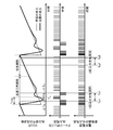
- FIG. 3 is a configuration diagram showing a phase synchronization circuit according to the first embodiment. It is explanatory drawing which shows the frequency of the output signal of VCO5, the current output from the charge pump 3, and the current output from the voltage-current converter 14.
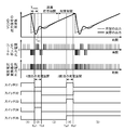
- FIG. 6 is a configuration diagram showing a phase locked loop circuit according to a second embodiment. It is explanatory drawing which shows the frequency of the output signal of VCO5, the current output from the charge pump 3, and the current output from the voltage-current converter 14.
- FIG. 7 is an explanatory diagram illustrating an operation of the switched capacitor circuit 22.
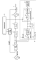
- FIG. 9 is a configuration diagram showing a phase locked loop circuit according to a third embodiment.
- FIG. 9 is an explanatory diagram showing convergence degrees C (1) to C (N) calculated N times by an arithmetic circuit 19.
- FIG. 9 is a configuration diagram showing a PLL circuit according to a fourth embodiment. Frequency of the output signal of the VCO 5, the current output from the charge pump 3 is an explanatory diagram showing a current and convergence time C Time output from the voltage-current converter 14.
- FIG. 11 is a configuration diagram showing a PLL circuit according to a fifth embodiment.
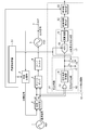
- FIG. 1 is a configuration diagram showing a phase locked loop circuit (hereinafter referred to as “PLL circuit”) according to the first embodiment.
- the reference signal source 1 outputs a reference signal having a constant frequency to the phase comparator 2.
- the phase comparator 2 compares the phase of the reference signal output from the reference signal source 1 with the phase of the divided signal output from the variable frequency divider 6. If the phase of the divided signal leads the phase of the reference signal, the phase comparator 2 outputs the phase error signal UP indicating the phase difference between the reference signal and the divided signal to the charge pump 3 and the OR circuit 13, respectively. Output to.
- phase comparator 2 If the phase of the divided signal lags the phase of the reference signal, the phase comparator 2 outputs the phase error signal DN indicating the phase difference between the reference signal and the divided signal to the charge pump 3 and the OR circuit 13, respectively. Output to.
- Each of the phase error signal UP and the phase error signal DN is a voltage signal.
- the charge pump 3 When the phase error signal UP is output from the phase comparator 2, the charge pump 3 outputs a positive polarity pulse current having a wider pulse width to the loop filter 4 as the phase difference indicated by the phase error signal UP increases.
- the phase error signal DN When the phase error signal DN is output from the phase comparator 2, the charge pump 3 outputs a negative pulse current having a wider pulse width to the loop filter 4 as the phase difference indicated by the phase error signal DN increases.
- the charge pump 3 does not output the pulse current to the loop filter 4 unless both the phase error signal UP and the phase error signal DN are output from the phase comparator 2.
- the loop filter 4 converts the pulse current output from the charge pump 3 into a voltage, smoothes the voltage, and the smoothed voltage is a voltage controlled oscillator (hereinafter, referred to as VCO (Voltage Controlled Oscillator)) 5 Output to.
- VCO Voltage Controlled Oscillator
- the VCO 5 outputs an output signal having a frequency corresponding to the voltage output from the loop filter 4 to each of the variable frequency divider 6 and the output terminal 7.
- the output signal of the VCO 5 is the output signal of the PLL circuit.
- the variable frequency divider 6 frequency-divides the output signal of the VCO 5 at the frequency division ratio indicated by the control signal output from the frequency controller 8 and outputs the frequency-divided output signal to the phase comparator 2 as a frequency-divided signal.
- the output terminal 7 is a terminal for outputting the output signal of the VCO 5 to the outside.
- the frequency controller 8 outputs a control signal indicating the frequency division ratio of the output signal to the variable frequency divider 6. Further, the frequency controller 8 outputs a control signal instructing on or off to the reset switch 16, and outputs a control signal instructing sampling of the charge amount to an analog-digital converter (hereinafter, referred to as “ADC”) 18. To do.
- the lock detection circuit 10 includes an integration circuit 11 and a convergence degree calculation circuit 17.
- the integrating circuit 11 includes a current output circuit 12, a capacitor 15 and a reset switch 16.
- the integrating circuit 11 integrates the phase difference indicated by the phase error signal UP output from the phase comparator 2 or the phase difference indicated by the phase error signal DN during a certain period within the transient response period of the output signal of the VCO 5.
- the integration circuit 11 outputs the integration result of the phase difference to the convergence degree calculation circuit 17 as a first integration result.
- the transient response period is a period during which the frequency of the output signal is causing damped oscillation, and the frequency of the output signal deviates from the desired frequency.
- the integration circuit 11 integrates the phase difference indicated by the phase error signal UP output from the phase comparator 2 or the phase difference indicated by the phase error signal DN during a certain period within the convergence period of the output signal of the VCO 5.
- the integration circuit 11 outputs the integration result of the phase difference to the convergence degree calculation circuit 17 as the second integration result.
- the convergence period is a period in which the frequency of the output signal substantially matches the desired frequency.
- the current output circuit 12 includes an OR circuit 13 and a voltage / current converter 14.
- the current output circuit 12 outputs to the ADC 18 a current corresponding to the phase difference indicated by the phase error signal UP output from the phase comparator 2 or the phase difference indicated by the phase error signal DN.
- the OR circuit 13 outputs the phase error signal UP to the voltage-current converter 14, and when the phase comparator 2 outputs the phase error signal DN, The phase error signal DN is output to the voltage / current converter 14.
- the voltage / current converter 14 converts the phase error signal UP into a current.
- the voltage / current converter 14 converts the phase error signal DN into a current.
- the capacitor 15 charges the electric charge according to the current output from the voltage-current converter 14 during a fixed period within the transient response period as the integration of the phase difference.
- the capacitor 15 charges the electric charge according to the current output from the voltage-current converter 14 during a fixed period within the convergence period as the integration of the phase difference.
- the reset switch 16 is turned on if the control signal output from the frequency controller 8 indicates “on”, and is off if the control signal output from the frequency controller 8 indicates “off”. become.
- the convergence degree calculation circuit 17 includes an ADC 18 and an arithmetic circuit 19.
- the convergence degree calculation circuit 17 calculates the degree of convergence of the output signal of the VCO 5 (hereinafter, referred to as “convergence degree”) from the first integration result and the second integration result output from the integration circuit 11. To do.
- the ADC 18 determines that the voltage corresponding to the charge amount of the charge charged during the fixed period within the transient response period. , The voltage applied to the capacitor 15 is sampled.
- the ADC 18 converts an analog value indicating the sampled voltage into a digital value (hereinafter, referred to as “first digital value”), and outputs the first digital value to the arithmetic circuit 19.
- first digital value a digital value
- the ADC 18 receives a control signal for instructing sampling of the charge amount from the frequency controller 8 within the convergence period
- the ADC 18 generates a capacitor corresponding to the charge amount of the charge charged during the constant period within the convergence period.
- the voltage applied to 15 is sampled.
- the ADC 18 converts the analog value indicating the sampled voltage into a digital value (hereinafter, referred to as “second digital value”), and outputs the second digital value to the arithmetic circuit 19.
- the arithmetic circuit 19 calculates the difference between the first digital value and the second digital value output from the ADC 18 as the degree of convergence of the output signal of the VCO 5. Alternatively, the arithmetic circuit 19 calculates the ratio between the first digital value and the second digital value output from the ADC 18 as the degree of convergence of the output signal of the VCO 5.
- FIG. 2 is an explanatory diagram showing the frequency of the output signal of the VCO 5, the current output from the charge pump 3, and the current output from the voltage-current converter 14.
- the frequency controller 8 controls the frequency division ratio of the output signal of the VCO 5 so that the frequency of the output signal of the VCO 5 changes in a sawtooth shape as shown by the dotted line in FIG.
- the frequency of the output signal of the VCO 5 is gradually increased by the frequency controller 8
- the change of the frequency division ratio under the control of the frequency controller 8 is small. If the change in the division ratio controlled by the frequency controller 8 is small, the frequency of the output signal changes following the change in the division ratio.
- the frequency of the output signal of the VCO 5 is sharply reduced by the frequency controller 8, the change of the frequency division ratio under the control of the frequency controller 8 is large.
- the PLL circuit shown in FIG. 1 is capable of calculating the degree of convergence of the output signal at the time point T m1 when the time T meas elapses from the time when the frequency of the output signal of the VCO 5 starts to sharply decrease.
- a circuit 10 is provided.
- the reference signal source 1 outputs a reference signal having a constant frequency to the phase comparator 2.
- the phase comparator 2 compares the phase of the reference signal with the phase of the divided signal output from the variable frequency divider 6. If the phase of the divided signal leads the phase of the reference signal, the phase comparator 2 outputs the phase error signal UP indicating the phase difference between the reference signal and the divided signal to the charge pump 3 and the OR circuit 13, respectively. Output to. If the phase of the divided signal lags the phase of the reference signal, the phase comparator 2 outputs the phase error signal DN indicating the phase difference between the reference signal and the divided signal to the charge pump 3 and the OR circuit 13, respectively. Output to.
- phase difference indicated by the phase error signal UP increases as the phase of the divided signal leads the phase of the reference signal and the degree of advance of the phase of the divided signal with respect to the reference signal increases.
- the phase difference indicated by the phase error signal DN becomes larger as the phase of the divided signal lags the phase of the reference signal and the degree of delay of the phase of the divided signal with respect to the reference signal increases.
- the charge pump 3 When the phase error signal UP is output from the phase comparator 2, the charge pump 3 raises the frequency of the output signal of the VCO 5 and therefore outputs a positive pulse current to the loop filter 4 as shown in FIG.
- the charge pump 3 outputs a positive polarity pulse current having a wider pulse width to the loop filter 4 as the phase difference indicated by the phase error signal UP increases. Therefore, when the frequency of the output signal of the VCO 5 is greatly increased, a positive pulse current having a wide pulse width is output to the loop filter 4, and when the frequency of the output signal is increased, a positive pulse current having a narrow pulse width is output. Is output to the loop filter 4. Since the rate of increase in the frequency of the output signal is constant during the convergence period in which the output signal of the VCO 5 is converged, the charge pump 3 repeatedly outputs a pulse current having a constant pulse width.
- the charge pump 3 When the phase error signal DN is output from the phase comparator 2, the charge pump 3 lowers the frequency of the output signal of the VCO 5, and thus outputs a negative pulse current to the loop filter 4 as shown in FIG.
- the charge pump 3 outputs a negative pulse current having a wider pulse width to the loop filter 4 as the phase difference indicated by the phase error signal DN increases. Therefore, when the frequency of the output signal of the VCO 5 is greatly reduced, a negative pulse current having a wide pulse width is output to the loop filter 4, and when the frequency of the output signal is reduced, a negative pulse current having a narrow pulse width is output. Is output to the loop filter 4.
- the loop filter 4 Upon receiving the pulse current from the charge pump 3, the loop filter 4 converts the pulse current into a voltage, smoothes the voltage, and outputs the smoothed voltage to the VCO 5. If the pulse current output from the charge pump 3 is a positive polarity pulse current, the smoothed voltage is high, and if the pulse current output from the charge pump 3 is a negative polarity pulse current, smoothing is performed. After that, the voltage becomes lower.
- the VCO 5 Upon receiving the smoothed voltage from the loop filter 4, the VCO 5 outputs an output signal having a frequency corresponding to the smoothed voltage to each of the variable frequency divider 6 and the output terminal 7.
- variable frequency divider 6 frequency-divides the output signal of the VCO 5 at the frequency division ratio indicated by the control signal output from the frequency controller 8 and outputs the frequency-divided output signal to the phase comparator 2 as a frequency-divided signal. To do.
- the OR circuit 13 When the phase comparator 2 outputs the phase error signal UP, the OR circuit 13 outputs the phase error signal UP to the voltage-current converter 14.
- the phase error signal DN When the phase error signal DN is output from the phase comparator 2, the OR circuit 13 outputs the phase error signal DN to the voltage-current converter 14.
- the voltage / current converter 14 Upon receiving the phase error signal UP from the OR circuit 13, the voltage / current converter 14 converts the phase error signal UP into a current.
- the voltage / current converter 14 Upon receiving the phase error signal DN from the OR circuit 13, the voltage / current converter 14 converts the phase error signal DN into a current.
- the frequency controller 8 calculates the degree of convergence of the output signal at the time point T m1 when the time T meas elapses from the time point when the frequency of the output signal of the VCO 5 starts to sharply decrease, and at time Ta1, A control signal instructing “off” is output to the reset switch 16.
- the reset switch 16 is turned off when receiving a control signal instructing “off” from the frequency controller 8.
- the reset switch 16 is turned on.
- the capacitor 15 starts charging the electric charge according to the current output from the voltage-current converter 14.
- the frequency controller 8 outputs a control signal instructing sampling of the charge amount to the ADC 18.
- the times Ta1 and Tb1 may be stored in the internal memory of the frequency controller 8 or may be given from the outside.
- the period (constant period) from time Ta1 to time Tb1 is within the transient response period. Further, the length of the period from the time Ta1 to time T m1, and the length of the period from the time point T m1 to time Tb1, the same length. Therefore, the time Ta1 is a time point earlier by the time ⁇ Ta than the time point T m1 , and the time Tb1 is a time point later than the time point T m1 by the time ⁇ Ta.
- the time Ta1 is the time when 9 [ ⁇ s] has elapsed from the time when the frequency of the output signal started to sharply decrease.
- Time Tb1 is a time point when 11 [ ⁇ s] has elapsed from the time point when the frequency of the output signal started to sharply decrease.
- the ADC 18 When the ADC 18 receives the control signal instructing sampling of the charge amount from the frequency controller 8, the ADC 18 samples the voltage V c applied to the capacitor 15. Since the voltage V c applied to the capacitor 15 is directly proportional to the charge amount of the electric charge in the capacitor 15, sampling the voltage V c applied to the capacitor 15 determines the charge amount of the electric charge in the capacitor 15. Equivalent to sampling. ADC18 converts the analog value indicating the voltage V c sampled into a first digital value V ADC1, and outputs a first digital value V ADC1 to the arithmetic circuit 19.
- the frequency controller 8 outputs a control signal for instructing sampling of the charge amount to the ADC 18, and then outputs a control signal for instructing “on” to the reset switch 16 in order to reset the capacitor 15 before the time Ta2. To do.
- the reset switch 16 is turned on when receiving a control signal instructing “on” from the frequency controller 8. When the reset switch 16 is turned on, the capacitor 15 discharges the charged electric charge.
- the frequency controller 8 outputs a control signal instructing “off” to the reset switch 16 at time Ta2.
- the reset switch 16 is turned off when receiving a control signal instructing “off” from the frequency controller 8.
- the capacitor 15 starts charging the electric charge according to the current output from the voltage-current converter 14.
- the frequency controller 8 outputs a control signal instructing sampling of the charge amount to the ADC 18.
- the times Ta2 and Tb2 may be stored in the internal memory of the frequency controller 8 or may be given from the outside.
- the period (constant period) from time Ta2 to time Tb2 is within the convergence period.
- the length of the period from time Ta2 to time Tb2 is the same as the length of the period from time Ta1 to time Tb1.
- the frequency controller 8 sets the period from time Ta2 to time Tb2 within the convergence period. It is possible to do so.
- the ADC 18 When the ADC 18 receives the control signal instructing sampling of the charge amount from the frequency controller 8, the ADC 18 samples the voltage V c applied to the capacitor 15. ADC18 converts the analog value indicating the voltage V c sampled into a second digital value V ADC2, and outputs a second digital value V ADC2 to the arithmetic circuit 19.
- the arithmetic circuit 19 calculates the difference between the first digital value V adc1 and the second digital value V adc2 as the convergence degree C of the output signal of the VCO 5 .
- the arithmetic circuit 19 sets the first digital value V adc1 and the second digital value V adc2 as the convergence degree C of the output signal of the VCO 5 as shown in the following expression (2).
- C V adc1 / V adc2 (2)
- the first embodiment described above integrates the phase difference between the frequency-divided signal and the reference signal in the VCO 5 during a fixed period within the transient response period of the output signal of the VCO 5 to obtain a fixed period within the convergence period of the output signal of the VCO 5.
- the integration circuit 11 that integrates the phase difference between the divided signal and the reference signal, the integration result of the phase difference in the integration circuit 11 during the fixed period within the transient response period, and the integration during the fixed period within the convergence period.
- the lock detection circuit 10 is configured so as to include a convergence degree calculation circuit 17 that calculates the degree of convergence of the output signal of the VCO 5 from the integration result of the phase difference in the circuit 11. Therefore, the lock detection circuit 10 can calculate the degree to which the output signal of the VCO 5 is converged.
- Embodiment 2 The lock detection circuit 10 shown in FIG. 1 integrates the phase difference between the frequency-divided signal and the reference signal during a fixed period within the transient response period of the output signal of the VCO 5 to obtain a fixed period within the convergence period of the output signal of the VCO 5.
- An integrating circuit 11 for integrating the phase difference between the divided signal and the reference signal is provided therein.
- the lock detection circuit 10 shown in FIG. 1 includes a convergence degree calculation circuit 17 that calculates the degree of convergence of the output signal of the VCO 5 from the first integration result and the second integration result output from the integration circuit 11. I have it.
- the lock detection circuit 10 includes an integration circuit 21 including a switched capacitor circuit 22, and a convergence degree for obtaining the charge amount of the charge in the capacitor 30 after the charge is charged in the negative direction by the switched capacitor circuit 22.
- the calculation circuit 41 may be included.
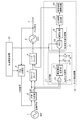
- FIG. 3 is a configuration diagram showing a PLL circuit according to the second embodiment.
- the same reference numerals as those in FIG. 1 indicate the same or corresponding portions, and thus the description thereof will be omitted.
- the frequency controller 9 outputs a control signal indicating the frequency division ratio of the output signal of the VC 05 to the variable frequency divider 6.
- the frequency controller 9 outputs a control signal instructing on or off to the switches 31 to 35, and outputs a control signal instructing sampling of the charge amount to the ADC 42 of the convergence degree calculation circuit 41.
- the integrating circuit 21 includes a current output circuit 12 and a switched capacitor circuit 22.
- the switched capacitor circuit 22 includes a capacitor 30 and switches 31 to 35.
- the switched capacitor circuit 22 charges the capacitor 30 in the positive direction according to the current output from the current output circuit 12 during a fixed period within the transient response period.
- the switched capacitor circuit 22 charges the capacitor 30 in the negative direction in accordance with the current output from the current output circuit 12 during a fixed period within the convergence period.
- the capacitor 30 has one end connected to one end of the switch 31 and the other end connected to one end of the switch 32.
- the capacitor 30 charges the charges in the positive direction according to the current output from the current output circuit 12, or charges the charges in the negative direction according to the current output from the current output circuit 12.
- the charge amount of the capacitor 30 corresponds to the integration result of the integration circuit 21.
- the switches 31 to 35 are turned on when receiving a control signal instructing “on” from the frequency controller 9, and turned off when receiving a control signal instructing “off” from the frequency controller 9.
- the switch 31 has one end connected to one end of the capacitor 30 and the other end connected to the ground.
- the switch 32 has one end connected to the other end of the capacitor 30 and the other end connected to the ground.
- the switch 33 has one end connected to the output side of the voltage-current converter 14 and the other end connected to the other end of the capacitor 30.
- the switch 34 has one end connected to the output side of the voltage-current converter 14 and the other end connected to one end of the capacitor 30.
- the switch 35 has one end connected to one end of the capacitor 30 and the other end connected to the input side of the ADC 42.
- the convergence degree calculation circuit 41 includes an ADC 42.
- the convergence degree calculation circuit 41 calculates the charge amount of the capacitor 30 after the charge is charged in the negative direction by the switched capacitor circuit 22 as the convergence degree of the output signal of VC05.
- the ADC 42 receives the control signal instructing the sampling from the frequency controller 9, the ADC 42 samples the voltage V c applied to the capacitor 30 as the voltage corresponding to the charge amount of the electric charge in the capacitor 30.
- the ADC 42 converts an analog value indicating the sampled voltage V c into a digital value V adc3 .
- the digital value V adc3 indicates the degree of convergence C of the output signal of VC05.
- FIG. 4 is an explanatory diagram showing the frequency of the output signal of the VCO 5, the current output from the charge pump 3, and the current output from the voltage-current converter 14.
- FIG. 5 is an explanatory diagram for explaining the operation of the switched capacitor circuit 22. Also in the PLL circuit shown in FIG. 3, it is assumed that the degree of convergence of the output signal at the time point T m1 at which the time T meas has elapsed from the time point when the frequency of the output signal of the VCO 5 starts to sharply decrease is calculated.
- the frequency controller 9 Before performing the calculation process of the convergence degree C, the frequency controller 9 outputs a control signal instructing "on” to the switches 31 and 32 and turning off “off", as shown in (1) of FIG.
- the control signal to instruct is output to the switches 33 to 35.
- the switches 31 and 32 receive a control signal for instructing “on” from the frequency controller 9, they are turned on as shown in (1) of FIG.
- the switches 33 to 35 receive the control signal instructing “OFF” from the frequency controller 9, they are turned off as shown in (1) of FIG. (1) of FIG. 5 shows the resetting of the capacitor 30, and all the charges charged in the capacitor 30 are discharged.
- the frequency controller 9 outputs a control signal instructing “on” to the switches 32 and 34 and a control signal instructing “off” at the switch 31 as shown in (1) of FIG. , 33, 35.
- the switches 32 and 34 receive the control signal for instructing “on” from the frequency controller 9, they are turned on as shown in (2) of FIG.
- the switches 31, 33, and 35 receive the control signal instructing "OFF” from the frequency controller 9, they are turned off as shown in (2) of FIG. (2) of FIG. 5 shows charging of the capacitor 30 in the transient response period, and the capacitor 30 is positively charged according to the current output from the voltage-current converter 14.
- the frequency controller 9 outputs a control signal for instructing “OFF” to the switches 31 to 35, as shown in (3) of FIG.
- the switches 31 to 35 receive the control signal instructing “OFF” from the frequency controller 9, they are turned off as shown in (3) of FIG. (3) of FIG. 5 shows holding of the electric charge charged by the capacitor 30.
- the frequency controller 9 outputs a control signal instructing “on” to the switches 31 and 33 and a control signal instructing “off” in the switch 32, as shown in (4) of FIG. , 34, 35.
- the switches 31 and 33 receive a control signal for instructing “on” from the frequency controller 9, they are turned on as shown in (4) of FIG.
- the switches 32, 34, and 35 receive the control signal instructing "off” from the frequency controller 9, they are turned off as shown in (4) of FIG. (4) of FIG. 5 shows the charging of the capacitor 30 during the convergence period, and the capacitor 30 is charged in the negative direction according to the current output from the voltage-current converter 14.
- the frequency controller 9 outputs a control signal instructing “on” to the switches 32 and 35 and outputs a control signal instructing “off” to the switch 31 as shown in (5) of FIG. , 33, 34.
- the frequency controller 9 also outputs a control signal instructing sampling of the charge amount to the ADC 42 of the convergence degree calculation circuit 41.
- the switches 32 and 35 receive a control signal for instructing “on” from the frequency controller 9, they are turned on as shown in (5) of FIG.
- the switches 31, 33, and 34 receive the control signal instructing “OFF” from the frequency controller 9, they are turned off as shown in (5) of FIG. (5) of FIG. 5 shows that the voltage applied to the capacitor 30 is sampled by the ADC 42.
- the ADC 42 When the ADC 42 receives the control signal instructing the sampling of the charge amount from the frequency controller 9, the ADC 42 samples the voltage V c applied to the capacitor 30 as the voltage corresponding to the charge amount of the capacitor 30.
- the ADC 42 converts an analog value indicating the sampled voltage V c into a digital value V adc3 .
- the digital value V adc3 indicates the degree of convergence C of the output signal of VC05. The closer the value of C is to 0, the closer the frequency of the output signal of the VCO 5 is to the desired frequency. Therefore , the digital value V adc3 within the transient response period is in a state of being close to convergence.
- the integration circuit 21 includes the current output circuit 12 and the switched capacitor circuit 22, and the convergence degree calculation circuit 41 determines the convergence degree of the output signal of the VC05 by the switched capacitor circuit 22 in the negative direction.
- the lock detection circuit 10 is configured so as to obtain the charge amount of the electric charge in the capacitor 30 after being charged. Therefore, the lock detection circuit 10 can calculate the degree of convergence of the output signal of the VCO 5.
- FIG. 6 is a configuration diagram showing a PLL circuit according to the third embodiment. 6, the same reference numerals as those in FIG. 1 indicate the same or corresponding portions, and thus the description thereof will be omitted.
- the frequency controller 51 outputs to the variable frequency divider 6 a control signal indicating the frequency division ratio of the output signal of the VC 05. Further, the frequency controller 51 outputs a control signal instructing on or off to the reset switch 16 and a control signal instructing sampling of the charge amount to the ADC 18, similarly to the frequency controller 8 shown in FIG. ..
- the frequency controller 51 switches the phase difference integration period to the integration circuit 11 and causes the integration circuit 11 to integrate and converge the phase difference in a fixed period within the transient response period. Each of the integration of the phase difference in a certain period of time is performed multiple times. Further, the frequency controller 51 instructs the convergence degree calculation circuit 17 to determine the degree of convergence of the output signal of the VCO 5 from the first integration result and the second integration result output from the integration circuit 11. Calculate each.
- the convergence time calculation unit 52 calculates the convergence time of the output signal of the VCO 5 from the respective convergence degrees calculated by the convergence degree calculation circuit 17.
- the configuration of the PLL circuit shown in FIG. 6 is a configuration in which a convergence time calculation unit 52 is added to the PLL circuit shown in FIG. 1 and a frequency controller 51 is used instead of the frequency controller 8.
- the present invention is not limited to this, and may be a PLL circuit in which the convergence time calculation unit 52 is added to the PLL circuit shown in FIG. 3 and the frequency controller 51 is used instead of the frequency controller 9.
- the PLL circuit shown in FIG. 1 calculates the degree of convergence C of the output signal only once at the time T m1 when the time T meas has elapsed from the time when the frequency of the output signal of the VCO 5 started to sharply decrease. ..
- the PLL circuit shown in FIG. 6 does not calculate the degree of convergence C only once, but switches the time T meas to switch the time T meas (1) to T meas (N) at each time point T m ( 1) Calculate the degree of convergence C (1) to C (N) of the output signal at T m (N ) to T m (N) , respectively. Specifically, it is as follows.
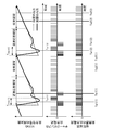
- FIG. 7 is an explanatory diagram showing the frequency of the output signal of the VCO 5, the current output from the charge pump 3, and the current output from the voltage-current converter 14.
- FIG. 7 corresponds to only two calculation of the convergence degrees C (1) and C (2).
- the frequency controller 51 calculates the degree of convergence of the output signal at the time point T m (1) at which the time T meas (1) has elapsed from the time point when the frequency of the output signal suddenly started to decrease, the frequency Ta1 is calculated.
- a control signal instructing “off” is output to the reset switch 16.
- the reset switch 16 is turned off when receiving a control signal instructing “off” from the frequency controller 51.
- the reset switch 16 is turned on.
- the capacitor 15 starts charging the electric charge according to the current output from the voltage-current converter 14.
- the frequency controller 51 outputs a control signal instructing sampling of the charge amount to the ADC 18.
- the times Ta1 (1) and Tb1 (1) may be stored in the internal memory of the frequency controller 51 or may be given from the outside.
- the period (constant period) from time Ta1 (1) to time Tb1 (1) is within the transient response period.
- the length of the period from time Ta1 (1) to time Tm (1) and the length of the period from time Tm (1) to time Tb1 (1) are the same.
- the ADC 18 When the ADC 18 receives the control signal instructing the sampling of the charge amount from the frequency controller 51, the ADC 18 samples the voltage V c applied to the capacitor 15. The ADC 18 converts an analog value indicating the sampled voltage V c into a first digital value V adc1 (1) and outputs the first digital value V adc1 (1) to the arithmetic circuit 19.
- the frequency controller 51 outputs a control signal instructing sampling of the charge amount to the ADC 18, and then resets the capacitor 15 before the time Ta2 (1). Therefore, the frequency controller 51 resets the control signal instructing “on” by the reset switch. Output to 16.
- the reset switch 16 is turned on when receiving a control signal instructing “on” from the frequency controller 51. When the reset switch 16 is turned on, the capacitor 15 discharges the charged electric charge.
- the frequency controller 51 outputs a control signal instructing “OFF” to the reset switch 16 at time Ta2 (1).
- the reset switch 16 is turned off when receiving a control signal instructing “off” from the frequency controller 51.
- the capacitor 15 starts charging the electric charge according to the current output from the voltage-current converter 14.
- the frequency controller 51 outputs a control signal instructing sampling of the charge amount to the ADC 18.
- the times Ta2 (1) and Tb2 (1) may be stored in the internal memory of the frequency controller 51 or may be given from the outside.
- the period (constant period) from time Ta2 (1) to time Tb2 (1) is within the convergence period.
- the length of the period from time Ta2 (1) to time Tb2 (1) is the same as the length of the period from time Ta1 (1) to time Tb1 (1).
- the exact period of the convergence period is unknown, but since the approximate convergence period can be known at the time of designing, in the frequency controller 51, the period from time Ta2 (1) to time Tb2 (1). Can be set within the convergence period.
- the ADC 18 When the ADC 18 receives the control signal instructing the sampling of the charge amount from the frequency controller 51, the ADC 18 samples the voltage V c applied to the capacitor 15. The ADC 18 converts the analog value indicating the sampled voltage V c into a second digital value V adc2 (1) and outputs the second digital value V adc2 (2) to the arithmetic circuit 19.
- the arithmetic circuit 19 uses the first digital value V adc1 (1) output from the ADC 18 and the second digital value as the convergence degree C (1) of the output signal of the VCO 5 as shown in the following expression (3).
- the difference from the value V adc2 (1) is calculated.
- C (1) V adc1 (1) -V adc2 (1) (3)
- the arithmetic circuit 19 calculates the difference between the first digital value V adc1 (1) and the second digital value V adc2 (1) as the degree of convergence C (1) of the output signal of the VCO 5 . ..
- this is merely an example, and the arithmetic circuit 19 sets the first digital value V adc1 (1) and the first digital value V adc1 (1) as the convergence degree C (1) of the output signal of the VCO 5 as shown in the following equation (4).
- the ratio of 2 to the digital value V adc2 (1) may be calculated.
- C (1) V adc1 (1) / V adc2 (1) (4)
- the frequency controller 51 outputs a control signal for instructing sampling of the charge amount to the ADC 18, and then resets the capacitor 15 before the time Ta (2), so that the control signal for instructing “on” is reset switch. Output to 16.
- the reset switch 16 is turned on when receiving a control signal instructing “on” from the frequency controller 51. When the reset switch 16 is turned on, the capacitor 15 discharges the charged electric charge.
- the frequency controller 51 calculates the degree of convergence of the output signal at the time point T m (n) when the time T meas (n) has elapsed from the time point when the frequency of the output signal suddenly started to decrease.
- a control signal instructing “off” is output to the reset switch 16.
- n 2, 3, ..., N.
- T meas (1) , T meas (2) , ..., T meas (N) are mutually different times. Therefore, the integration period of the phase difference at the convergence degrees C (1) to C (N) N times is different.
- the reset switch 16 is turned off when receiving a control signal instructing “off” from the frequency controller 51. When the reset switch 16 is turned off, the capacitor 15 starts charging the electric charge according to the current output from the voltage-current converter 14.
- the frequency controller 51 outputs a control signal instructing sampling of the charge amount to the ADC 18.
- the times Ta1 (n) and Tb1 (n) may be stored in the internal memory of the frequency controller 51 or may be given from the outside.
- the period (constant period) from time Ta1 (n) to time Tb1 (n) is within the transient response period.
- the length of the period from time Ta1 (n) to time Tm (n) and the length of the period from time Tm (n) to time Tb1 (n) are the same.
- the length of the period from time Ta1 (n) to time Tb1 (n) is the same as the length of the period from time Ta1 (1) to time Tb1 (1).
- the ADC 18 When the ADC 18 receives the control signal instructing the sampling of the charge amount from the frequency controller 51, the ADC 18 samples the voltage V c applied to the capacitor 15. The ADC 18 converts an analog value indicating the sampled voltage V c into a first digital value V adc1 (n) and outputs the first digital value V adc1 (n) to the arithmetic circuit 19.
- the frequency controller 51 outputs a control signal instructing sampling of the charge amount to the ADC 18, and then resets the capacitor 15 before the time Ta2 (n), so that the control signal instructing "on” is reset switch. Output to 16.
- the reset switch 16 is turned on when receiving a control signal instructing “on” from the frequency controller 51. When the reset switch 16 is turned on, the capacitor 15 discharges the charged electric charge.
- the frequency controller 51 outputs a control signal instructing “off” to the reset switch 16 at time Ta2 (n).
- the reset switch 16 is turned off when receiving a control signal instructing “off” from the frequency controller 51.
- the capacitor 15 starts charging the electric charge according to the current output from the voltage-current converter 14.
- the frequency controller 51 outputs a control signal instructing sampling of the charge amount to the ADC 18.
- the times Ta2 (n) and Tb2 (n) may be stored in the internal memory of the frequency controller 51 or may be given from the outside.
- the period (constant period) from time Ta2 (n) to time Tb2 (n) is within the convergence period.
- the length of the period from time Ta2 (n) to time Tb2 (n) is the same as the length of the period from time Ta1 (n) to time Tb1 (n).
- the exact period of the convergence period is unknown, but since the approximate convergence period can be known at the time of design, in the frequency controller 51, the period from time Ta2 (n) to time Tb2 (n). Can be set within the convergence period.
- the ADC 18 When the ADC 18 receives the control signal instructing the sampling of the charge amount from the frequency controller 51, the ADC 18 samples the voltage V c applied to the capacitor 15. The ADC 18 converts an analog value indicating the sampled voltage V c into a second digital value V adc2 (n) and outputs the second digital value V adc2 (n) to the arithmetic circuit 19.
- the arithmetic circuit 19 uses the first digital value V adc1 (n) output from the ADC 18 and the second digital value as the convergence degree C (n) of the output signal of the VCO 5 as shown in the following equation (5).
- the difference from the value V adc2 (n) is calculated.
- C (n) V adc1 (n) -V adc2 (n) (5)
- the arithmetic circuit 19 calculates the difference between the first digital value V adc1 (n) and the second digital value V adc2 (n) as the degree of convergence C (n) of the output signal of the VCO 5 . ..
- this is merely an example, and the arithmetic circuit 19 sets the first digital value V adc1 (n) and the first digital value V adc1 (n) as the convergence degree C (n) of the output signal of the VCO 5 as shown in the following equation (6).
- the ratio of 2 to the digital value V adc2 (n) may be calculated.
- C (n) V adc1 (n) / V adc2 (n) (6)
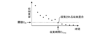
- FIG. 8 is an explanatory diagram showing the convergence degrees C (1) to C (N) calculated N times by the arithmetic circuit 19.
- black circles indicate the convergence degrees C (1) to C (N) calculated N times by the arithmetic circuit 19.
- the time on the horizontal axis in FIG. 8 represents the time from the time point when the frequency of the output signal starts to sharply decrease to the time point T m (n) .
- the convergence time calculation unit 52 compares the convergence degrees C (1) to C (N) calculated N times by the convergence degree calculation circuit 17 with the threshold value C th .
- the threshold value C th may be stored in the internal memory of the convergence time calculation unit 52 or may be given from the outside.
- the convergence time calculation unit 52 searches for the convergence degree C (n) having the largest value among the convergence degrees (n) smaller than the threshold value Cth among the convergence degrees C (1) to C (N). To do.
- the convergence time calculation unit 52 determines that the output signal of the VCO 5 has converged at the time point T m (n) corresponding to the searched convergence degree C (n), and the time point from the time point when the output signal frequency sharply starts to decrease.
- the time to T m (n) is calculated as the convergence time C Time of the output signal of the VCO 5.
- the integration circuit 11 switches the integration period of the phase difference while integrating the integration of the phase difference in a fixed period within the transient response period and the integration of the phase difference in a fixed period within the convergence period. Each of them is performed a plurality of times, and each first integration result and each second integration result is output to the convergence degree calculation circuit 17. Further, the degree-of-convergence calculation circuit 17 calculates the degree of convergence of the output signal of the VCO 5 from each of the first integration result and the respective second integration result output from the integration circuit 11. Therefore, the lock detection circuit 10 can calculate the convergence time C Time of the output signal of the VCO 5.
- a PLL circuit including a time zone detection unit 53 that detects a time zone in which the output signal of the VCO 5 can be used from the convergence time C Time calculated by the convergence time calculation unit 52 will be described.
- FIG. 9 is a configuration diagram showing a PLL circuit according to the fourth embodiment. 9, the same reference numerals as those in FIGS. 1, 3 and 6 indicate the same or corresponding portions, and thus the description thereof will be omitted.
- the time zone detection unit 53 detects the available time zone of the output signal of the VCO 5 from the convergence time C Time calculated by the convergence time calculation unit 52.
- the configuration of the PLL circuit shown in FIG. 9 is a configuration in which the time zone detection unit 53 is added to the PLL circuit shown in FIG.
- the present invention is not limited to this, and in the PLL circuit shown in FIG. 3, a convergence time calculation unit 52 and a time zone detection unit 53 are added, and a frequency controller 51 is used instead of the frequency controller 9. It may be.
- the operation of the PLL circuit shown in FIG. 9 will be described.
- the components other than the time zone detection unit 53 are the same as those of the PLL circuit shown in FIG. 6, only the operation of the time zone detection unit 53 will be described here.
- a communication system (not shown) that transmits and receives a communication signal by using the output signal of the VCO 5.
- it is necessary to use a converged output signal. If the communication system uses an output signal that has not converged, it may not be possible to realize highly accurate transmission and reception of the communication signal.
- a radar system (not shown) that performs signal processing of the radar signal by using the output signal of the VCO 5.
- the radar system in order to realize highly accurate signal processing, it is necessary to use the converged output signal. If the radar system uses an output signal that has not converged, it may not be possible to realize highly accurate signal processing.
- FIG. 10 is an explanatory diagram showing the frequency of the output signal of the VCO 5, the current output from the charge pump 3, the current output from the voltage-current converter 14, and the convergence time C Time .
- the time zone detection unit 53 determines, as the available time zone of the output signal of the VCO 5, from the convergence time C Time calculated by the convergence time calculation unit 52, when the frequency of the output signal of the VCO 5 next sharply starts to decrease. To detect the time zone until.
- the time zone detection unit 53 monitors the control signal indicating the frequency division ratio output from the frequency controller 51 to the variable frequency divider 6, thereby recognizing the time when the frequency of the output signal of the VCO 5 starts to sharply decrease. can do.
- the lock detection circuit 10 includes the time zone detection unit 53 that detects the time zone in which the output signal of the VCO 5 can be used from the convergence time C Time calculated by the convergence time calculation unit 52. Configured. Therefore, the lock detection circuit 10 can output the output signal of the VCO 5 in the available time zone to the communication system or the radar system.
- Embodiment 5 a PLL circuit including a convergence time adjustment circuit 54 that applies a current to the input side of the loop filter 4 will be described so that the convergence time C Time calculated by the convergence time calculation unit 52 becomes short.
- FIG. 11 is a configuration diagram showing a PLL circuit according to the fifth embodiment. 11, the same reference numerals as those in FIG. 1, FIG. 3, FIG. 6 and FIG.
- the convergence time adjustment circuit 54 is a circuit that applies a current to the input side of the loop filter 4 so that the convergence time C Time calculated by the convergence time calculation unit 52 becomes short.
- the configuration of the PLL circuit shown in FIG. 11 is a configuration in which a convergence time adjusting circuit 54 is added to the PLL circuit shown in FIG.
- the present invention is not limited to this, and in the PLL circuit shown in FIG. 3, a convergence time calculation unit 52 and a convergence time adjustment circuit 54 are added, and a frequency controller 51 is used instead of the frequency controller 9. It may be.
- loop filter 4 Upon receiving the pulse current from charge pump 3, loop filter 4 converts the pulse current into a voltage, smoothes the voltage, and outputs the smoothed voltage to VCO 5, as in the first embodiment.
- the voltage output from the loop filter 4 to the VCO 5 changes when another pulse current is input to the loop filter 4 in addition to the pulse current output from the charge pump 3, so that the output signal of the VCO 5 changes.
- the convergence time C Time of is changed.
- the convergence time adjustment circuit 54 stores the convergence time C Time calculated by the convergence time calculation unit 52 while changing the magnitude or polarity of the pulse current applied to the input side of the loop filter 4.
- the convergence time adjustment circuit 54 identifies the pulse current corresponding to the shortest convergence time C Time of the stored plurality of convergence times C Time among the pulse currents applied to the input side of the loop filter 4. After that, the convergence time adjustment circuit 54 applies the specified pulse current to the input side of the loop filter 4.
- the lock detection circuit is provided with the convergence time adjustment circuit 54 that applies a current to the input side of the loop filter 4 so that the convergence time C Time calculated by the convergence time calculation unit 52 becomes short. Configured 10. Therefore, the lock detection circuit 10 of the fifth embodiment can shorten the convergence time C Time as compared with the lock detection circuits 10 of the first to fourth embodiments.
- the invention of the present application is capable of freely combining the embodiments, modifying any constituent element of each embodiment, or omitting any constituent element in each embodiment. ..
- the present invention is suitable for a lock detection circuit that calculates the degree to which the output signal of the phase locked loop has converged. Further, the present invention is suitable for a phase locked loop circuit for calculating the degree of convergence of the output signal of the voltage controlled oscillator.
- 1 reference signal source 2 phase comparator, 3 charge pump, 4 loop filter, 5 VCO, 6 variable frequency divider, 7 output terminals, 8 and 9 frequency controller, 10 lock detection circuit, 11 integration circuit, 12 current output Circuit, 13 OR circuit, 14 voltage / current converter, 15 capacitor, 16 reset switch, 17 convergence degree calculation circuit, 18 ADC, 19 arithmetic circuit, 21 integrating circuit, 22 switched capacitor circuit, 30 capacitor, 31-35 switch, 41 convergence degree calculation circuit, 42 ADC, 51 frequency controller, 52 convergence time calculation unit, 53 time zone detection unit, 54 convergence time adjustment circuit.
Landscapes
- Stabilization Of Oscillater, Synchronisation, Frequency Synthesizers (AREA)
Abstract
VCO(5)の出力信号における過渡応答期間内の一定期間中に、VCO(5)における分周信号と基準信号との位相差を積分し、VCO(5)の出力信号における収束期間内の一定期間中に、分周信号と基準信号との位相差を積分する積分回路(11)と、過渡応答期間内の一定期間中の積分回路(11)における位相差の積分結果と、収束期間内の一定期間中の積分回路(11)における位相差の積分結果とから、VCO(5)の出力信号が収束している度合を算出する収束度合算出回路(17)とを備えるように、ロック検出回路(10)を構成した。
Description
この発明は、位相同期回路の出力信号が収束している度合を算出するロック検出回路と、電圧制御発振器の出力信号が収束している度合を算出する位相同期回路とに関するものである。
位相同期回路(以下、「PLL(Phase Locked Loop)回路」と称する)は、基準信号を出力する基準信号源と、基準信号源から出力された基準信号と後述の可変分周器から出力された分周信号との位相差を出力する位相比較器とを備えている。
また、PLL回路は、位相比較器から出力された位相差に従って出力信号の周波数が変化する電圧制御発振器と、電圧制御発振器の出力信号を分周し、分周後の出力信号を分周信号として、位相比較器に出力する可変分周器とを備えている。
PLL回路は、可変分周器における出力信号の分周比を変えることで、電圧制御発振器の出力信号の周波数を変えることができる。
また、PLL回路は、位相比較器から出力された位相差に従って出力信号の周波数が変化する電圧制御発振器と、電圧制御発振器の出力信号を分周し、分周後の出力信号を分周信号として、位相比較器に出力する可変分周器とを備えている。
PLL回路は、可変分周器における出力信号の分周比を変えることで、電圧制御発振器の出力信号の周波数を変えることができる。
PLL回路の性能指標の1つとして、収束時間がある。収束時間は、出力信号の周波数を急峻に変化させたときに、出力信号の周波数が安定するまでに要する時間である。
以下の非特許文献1には、基準信号と分周信号との位相差が閾値以下になれば、出力信号が収束していると判定するロック検出回路が開示されている。
以下の非特許文献1には、基準信号と分周信号との位相差が閾値以下になれば、出力信号が収束していると判定するロック検出回路が開示されている。
Peadar Forbes, Ian Collins著「Lock Detect on the ADF4xxx Family of PLL Synthesizers」, Analog Devices社 アプリケーションノート AN-873
非特許文献1に開示されているロック検出回路は、基準信号と分周信号との位相差が閾値以下になれば、出力信号が収束していると判定する。しかし、位相差は、出力信号の分周比を変えることで、出力信号の周波数を急峻に変化させると、安定するまでの間、減衰振動を生じる。したがって、単に位相差と閾値を比較するだけでは、出力信号が、どの程度、収束しているかを算出することができないという課題があった。
この発明は上記のような課題を解決するためになされたもので、出力信号が収束している度合を算出することができるロック検出回路及び位相同期回路を得ることを目的とする。
この発明に係るロック検出回路は、位相同期回路の出力信号における過渡応答期間内の一定期間中に、位相同期回路における分周信号と基準信号との位相差を積分し、位相同期回路の出力信号における収束期間内の一定期間中に、分周信号と基準信号との位相差を積分する積分回路と、過渡応答期間内の一定期間中の積分回路における位相差の積分結果と、収束期間内の一定期間中の積分回路における位相差の積分結果とから、位相同期回路の出力信号が収束している度合を算出する収束度合算出回路とを備えるようにしたものである。
この発明によれば、収束度合算出回路が、過渡応答期間内の一定期間中の積分回路における位相差の積分結果と、収束期間内の一定期間中の積分回路における位相差の積分結果とから、位相同期回路の出力信号が収束している度合を算出するように、ロック検出回路を構成した。したがって、この発明に係るロック検出回路は、位相同期回路の出力信号が収束している度合を算出することができる。
以下、この発明をより詳細に説明するために、この発明を実施するための形態について、添付の図面に従って説明する。
実施の形態1.
図1は、実施の形態1に係る位相同期回路(以下、「PLL回路」と称する)を示す構成図である。
図1において、基準信号源1は、周波数が一定の基準信号を位相比較器2に出力する。
位相比較器2は、基準信号源1から出力された基準信号の位相と、可変分周器6から出力された分周信号の位相とを比較する。
位相比較器2は、分周信号の位相が基準信号の位相よりも進んでいれば、基準信号と分周信号との位相差を示す位相誤差信号UPをチャージポンプ3及び論理和回路13のそれぞれに出力する。
位相比較器2は、分周信号の位相が基準信号の位相よりも遅れていれば、基準信号と分周信号との位相差を示す位相誤差信号DNをチャージポンプ3及び論理和回路13のそれぞれに出力する。
位相誤差信号UP及び位相誤差信号DNのそれぞれは、電圧信号である。
図1は、実施の形態1に係る位相同期回路(以下、「PLL回路」と称する)を示す構成図である。
図1において、基準信号源1は、周波数が一定の基準信号を位相比較器2に出力する。
位相比較器2は、基準信号源1から出力された基準信号の位相と、可変分周器6から出力された分周信号の位相とを比較する。
位相比較器2は、分周信号の位相が基準信号の位相よりも進んでいれば、基準信号と分周信号との位相差を示す位相誤差信号UPをチャージポンプ3及び論理和回路13のそれぞれに出力する。
位相比較器2は、分周信号の位相が基準信号の位相よりも遅れていれば、基準信号と分周信号との位相差を示す位相誤差信号DNをチャージポンプ3及び論理和回路13のそれぞれに出力する。
位相誤差信号UP及び位相誤差信号DNのそれぞれは、電圧信号である。
チャージポンプ3は、位相比較器2から位相誤差信号UPが出力されると、位相誤差信号UPが示す位相差が大きい程、パルス幅が広い正極性のパルス電流をループフィルタ4に出力する。
チャージポンプ3は、位相比較器2から位相誤差信号DNが出力されると、位相誤差信号DNが示す位相差が大きい程、パルス幅が広い負極性のパルス電流をループフィルタ4に出力する。
チャージポンプ3は、位相比較器2から位相誤差信号UP及び位相誤差信号DNの双方が出力されていなければ、パルス電流をループフィルタ4に出力しない。
チャージポンプ3は、位相比較器2から位相誤差信号DNが出力されると、位相誤差信号DNが示す位相差が大きい程、パルス幅が広い負極性のパルス電流をループフィルタ4に出力する。
チャージポンプ3は、位相比較器2から位相誤差信号UP及び位相誤差信号DNの双方が出力されていなければ、パルス電流をループフィルタ4に出力しない。
ループフィルタ4は、チャージポンプ3から出力されたパルス電流を電圧に変換して、電圧の平滑化を行い、平滑化後の電圧を電圧制御発振器(以下、VCO(Voltage Controlled Oscillator)と称する)5に出力する。
VCO5は、ループフィルタ4から出力された電圧に対応する周波数の出力信号を可変分周器6及び出力端子7のそれぞれに出力する。VCO5の出力信号は、PLL回路の出力信号である。
VCO5は、ループフィルタ4から出力された電圧に対応する周波数の出力信号を可変分周器6及び出力端子7のそれぞれに出力する。VCO5の出力信号は、PLL回路の出力信号である。
可変分周器6は、周波数制御器8から出力された制御信号が示す分周比で、VCO5の出力信号を分周し、分周後の出力信号を分周信号として位相比較器2に出力する。
出力端子7は、VCO5の出力信号を外部に出力するための端子である。
周波数制御器8は、出力信号の分周比を示す制御信号を可変分周器6に出力する。
また、周波数制御器8は、オン又はオフを指示する制御信号をリセットスイッチ16に出力し、充電量のサンプリングを指示する制御信号をアナログデジタル変換器(以下、「ADC」と称する)18に出力する。
出力端子7は、VCO5の出力信号を外部に出力するための端子である。
周波数制御器8は、出力信号の分周比を示す制御信号を可変分周器6に出力する。
また、周波数制御器8は、オン又はオフを指示する制御信号をリセットスイッチ16に出力し、充電量のサンプリングを指示する制御信号をアナログデジタル変換器(以下、「ADC」と称する)18に出力する。
ロック検出回路10は、積分回路11及び収束度合算出回路17を備えている。
積分回路11は、電流出力回路12、コンデンサ15及びリセットスイッチ16を備えている。
積分回路11は、VCO5の出力信号における過渡応答期間内の一定期間中に、位相比較器2から出力された位相誤差信号UPが示す位相差又は位相誤差信号DNが示す位相差を積分する。積分回路11は、当該位相差の積分結果を第1の積分結果として収束度合算出回路17に出力する。過渡応答期間は、出力信号の周波数が減衰振動を生じている期間であり、出力信号の周波数は、所望周波数からずれている。
また、積分回路11は、VCO5の出力信号における収束期間内の一定期間中に、位相比較器2から出力された位相誤差信号UPが示す位相差又は位相誤差信号DNが示す位相差を積分する。積分回路11は、当該位相差の積分結果を第2の積分結果として収束度合算出回路17に出力する。収束期間は、出力信号の周波数が所望周波数とほぼ一致している期間である。
積分回路11は、電流出力回路12、コンデンサ15及びリセットスイッチ16を備えている。
積分回路11は、VCO5の出力信号における過渡応答期間内の一定期間中に、位相比較器2から出力された位相誤差信号UPが示す位相差又は位相誤差信号DNが示す位相差を積分する。積分回路11は、当該位相差の積分結果を第1の積分結果として収束度合算出回路17に出力する。過渡応答期間は、出力信号の周波数が減衰振動を生じている期間であり、出力信号の周波数は、所望周波数からずれている。
また、積分回路11は、VCO5の出力信号における収束期間内の一定期間中に、位相比較器2から出力された位相誤差信号UPが示す位相差又は位相誤差信号DNが示す位相差を積分する。積分回路11は、当該位相差の積分結果を第2の積分結果として収束度合算出回路17に出力する。収束期間は、出力信号の周波数が所望周波数とほぼ一致している期間である。
電流出力回路12は、論理和回路13及び電圧電流変換器14を備えている。
電流出力回路12は、位相比較器2から出力された位相誤差信号UPが示す位相差又は位相誤差信号DNが示す位相差に対応する電流をADC18に出力する。
論理和回路13は、位相比較器2から位相誤差信号UPが出力されると、位相誤差信号UPを電圧電流変換器14に出力し、位相比較器2から位相誤差信号DNが出力されると、位相誤差信号DNを電圧電流変換器14に出力する。
電圧電流変換器14は、論理和回路13から位相誤差信号UPを受けると、位相誤差信号UPを電流に変換する。
電圧電流変換器14は、論理和回路13から位相誤差信号DNを受けると、位相誤差信号DNを電流に変換する。
電流出力回路12は、位相比較器2から出力された位相誤差信号UPが示す位相差又は位相誤差信号DNが示す位相差に対応する電流をADC18に出力する。
論理和回路13は、位相比較器2から位相誤差信号UPが出力されると、位相誤差信号UPを電圧電流変換器14に出力し、位相比較器2から位相誤差信号DNが出力されると、位相誤差信号DNを電圧電流変換器14に出力する。
電圧電流変換器14は、論理和回路13から位相誤差信号UPを受けると、位相誤差信号UPを電流に変換する。
電圧電流変換器14は、論理和回路13から位相誤差信号DNを受けると、位相誤差信号DNを電流に変換する。
コンデンサ15は、位相差の積分として、過渡応答期間内の一定期間中に、電圧電流変換器14から出力された電流に従って電荷を充電する。
コンデンサ15は、位相差の積分として、収束期間内の一定期間中に、電圧電流変換器14から出力された電流に従って電荷を充電する。
リセットスイッチ16は、周波数制御器8から出力された制御信号が“オン”を指示していればオンになり、周波数制御器8から出力された制御信号が“オフ”を指示していればオフになる。
コンデンサ15は、位相差の積分として、収束期間内の一定期間中に、電圧電流変換器14から出力された電流に従って電荷を充電する。
リセットスイッチ16は、周波数制御器8から出力された制御信号が“オン”を指示していればオンになり、周波数制御器8から出力された制御信号が“オフ”を指示していればオフになる。
収束度合算出回路17は、ADC18及び演算回路19を備えている。
収束度合算出回路17は、積分回路11から出力された第1の積分結果と第2の積分結果とから、VCO5の出力信号が収束している度合(以下、「収束度合」と称する)を算出する。
収束度合算出回路17は、積分回路11から出力された第1の積分結果と第2の積分結果とから、VCO5の出力信号が収束している度合(以下、「収束度合」と称する)を算出する。
ADC18は、過渡応答期間内に、周波数制御器8から充電量のサンプリングを指示する制御信号を受けると、過渡応答期間内の一定期間中に充電された電荷の充電量に相当している電圧として、コンデンサ15に印加されている電圧をサンプリングする。
ADC18は、サンプリングした電圧を示すアナログ値をデジタル値(以下、「第1のデジタル値」と称する)に変換し、第1のデジタル値を演算回路19に出力する。
ADC18は、収束期間内に、周波数制御器8から充電量のサンプリングを指示する制御信号を受けると、収束期間内の一定期間中に充電された電荷の充電量に相当している電圧として、コンデンサ15に印加されている電圧をサンプリングする。
ADC18は、サンプリングした電圧を示すアナログ値をデジタル値(以下、「第2のデジタル値」と称する)に変換し、第2のデジタル値を演算回路19に出力する。
ADC18は、サンプリングした電圧を示すアナログ値をデジタル値(以下、「第1のデジタル値」と称する)に変換し、第1のデジタル値を演算回路19に出力する。
ADC18は、収束期間内に、周波数制御器8から充電量のサンプリングを指示する制御信号を受けると、収束期間内の一定期間中に充電された電荷の充電量に相当している電圧として、コンデンサ15に印加されている電圧をサンプリングする。
ADC18は、サンプリングした電圧を示すアナログ値をデジタル値(以下、「第2のデジタル値」と称する)に変換し、第2のデジタル値を演算回路19に出力する。
演算回路19は、VCO5の出力信号の収束度合として、ADC18から出力された第1のデジタル値と第2のデジタル値との差分を算出する。あるいは、演算回路19は、VCO5の出力信号の収束度合として、ADC18から出力された第1のデジタル値と第2のデジタル値との比を算出する。
次に、図1に示すPLL回路の動作について説明する。
ここでは、PLL回路が、周波数が鋸波状に変化する出力信号を生成する例を説明する。
図2は、VCO5の出力信号の周波数、チャージポンプ3から出力される電流及び電圧電流変換器14から出力される電流を示す説明図である。
ここでは、PLL回路が、周波数が鋸波状に変化する出力信号を生成する例を説明する。
図2は、VCO5の出力信号の周波数、チャージポンプ3から出力される電流及び電圧電流変換器14から出力される電流を示す説明図である。
周波数制御器8は、VCO5の出力信号の周波数が、図2の点線で表されるような鋸波状に変化するように、出力信号の分周比を制御する。
周波数制御器8によって、VCO5の出力信号の周波数が徐々に上昇される場合、周波数制御器8の制御による分周比の変化は小さい。周波数制御器8が制御する分周比の変化が小さければ、出力信号の周波数は、分周比の変化に追従して変化する。
周波数制御器8によって、VCO5の出力信号の周波数が急峻に低下される場合、周波数制御器8の制御による分周比の変化が大きい。周波数制御器8が制御する分周比の変化が大きければ、出力信号の周波数は、分周比の変化に追従しきれないため、減衰振動を生じる。
したがって、VCO5の出力信号における実際の周波数は、図2の実線で表されるような波形となる。
図1に示すPLL回路は、VCO5の出力信号の周波数が急峻に低下を開始した時点から、Tmeasの時間を経過した時点Tm1での出力信号の収束度合を算出することが可能なロック検出回路10を備えている。
周波数制御器8によって、VCO5の出力信号の周波数が徐々に上昇される場合、周波数制御器8の制御による分周比の変化は小さい。周波数制御器8が制御する分周比の変化が小さければ、出力信号の周波数は、分周比の変化に追従して変化する。
周波数制御器8によって、VCO5の出力信号の周波数が急峻に低下される場合、周波数制御器8の制御による分周比の変化が大きい。周波数制御器8が制御する分周比の変化が大きければ、出力信号の周波数は、分周比の変化に追従しきれないため、減衰振動を生じる。
したがって、VCO5の出力信号における実際の周波数は、図2の実線で表されるような波形となる。
図1に示すPLL回路は、VCO5の出力信号の周波数が急峻に低下を開始した時点から、Tmeasの時間を経過した時点Tm1での出力信号の収束度合を算出することが可能なロック検出回路10を備えている。
まず、基準信号源1は、周波数が一定の基準信号を位相比較器2に出力する。
位相比較器2は、基準信号源1から基準信号を受けると、基準信号の位相と、可変分周器6から出力された分周信号の位相とを比較する。
位相比較器2は、分周信号の位相が基準信号の位相よりも進んでいれば、基準信号と分周信号との位相差を示す位相誤差信号UPをチャージポンプ3及び論理和回路13のそれぞれに出力する。
位相比較器2は、分周信号の位相が基準信号の位相よりも遅れていれば、基準信号と分周信号との位相差を示す位相誤差信号DNをチャージポンプ3及び論理和回路13のそれぞれに出力する。
位相比較器2は、基準信号源1から基準信号を受けると、基準信号の位相と、可変分周器6から出力された分周信号の位相とを比較する。
位相比較器2は、分周信号の位相が基準信号の位相よりも進んでいれば、基準信号と分周信号との位相差を示す位相誤差信号UPをチャージポンプ3及び論理和回路13のそれぞれに出力する。
位相比較器2は、分周信号の位相が基準信号の位相よりも遅れていれば、基準信号と分周信号との位相差を示す位相誤差信号DNをチャージポンプ3及び論理和回路13のそれぞれに出力する。
位相誤差信号UPが示す位相差は、分周信号の位相が、基準信号の位相よりも進んでおり、基準信号に対する分周信号の位相の進み具合が大きくなるほど大きくなる。
位相誤差信号DNが示す位相差は、分周信号の位相が、基準信号の位相よりも遅れており、基準信号に対する分周信号の位相の遅れ具合が大きくなるほど大きくなる。
位相誤差信号DNが示す位相差は、分周信号の位相が、基準信号の位相よりも遅れており、基準信号に対する分周信号の位相の遅れ具合が大きくなるほど大きくなる。
チャージポンプ3は、位相比較器2から位相誤差信号UPが出力されると、VCO5の出力信号の周波数を上げるため、図2に示すように、正極性のパルス電流をループフィルタ4に出力する。
チャージポンプ3は、位相誤差信号UPが示す位相差が大きい程、パルス幅が広い正極性のパルス電流をループフィルタ4に出力する。したがって、VCO5の出力信号の周波数を大きく上げるときは、パルス幅が広い正極性のパルス電流をループフィルタ4に出力し、出力信号の周波数を小さく上げるときは、パルス幅が狭い正極性のパルス電流をループフィルタ4に出力する。VCO5の出力信号が収束している収束期間では、出力信号の周波数の上昇率が一定であるため、チャージポンプ3からは、一定のパルス幅のパルス電流が繰り返し出力される。
チャージポンプ3は、位相誤差信号UPが示す位相差が大きい程、パルス幅が広い正極性のパルス電流をループフィルタ4に出力する。したがって、VCO5の出力信号の周波数を大きく上げるときは、パルス幅が広い正極性のパルス電流をループフィルタ4に出力し、出力信号の周波数を小さく上げるときは、パルス幅が狭い正極性のパルス電流をループフィルタ4に出力する。VCO5の出力信号が収束している収束期間では、出力信号の周波数の上昇率が一定であるため、チャージポンプ3からは、一定のパルス幅のパルス電流が繰り返し出力される。
チャージポンプ3は、位相比較器2から位相誤差信号DNが出力されると、VCO5の出力信号の周波数を下げるため、図2に示すように、負極性のパルス電流をループフィルタ4に出力する。
チャージポンプ3は、位相誤差信号DNが示す位相差が大きい程、パルス幅が広い負極性のパルス電流をループフィルタ4に出力する。したがって、VCO5の出力信号の周波数を大きく下げるときは、パルス幅が広い負極性のパルス電流をループフィルタ4に出力し、出力信号の周波数を小さく下げるときは、パルス幅が狭い負極性のパルス電流をループフィルタ4に出力する。
チャージポンプ3は、位相誤差信号DNが示す位相差が大きい程、パルス幅が広い負極性のパルス電流をループフィルタ4に出力する。したがって、VCO5の出力信号の周波数を大きく下げるときは、パルス幅が広い負極性のパルス電流をループフィルタ4に出力し、出力信号の周波数を小さく下げるときは、パルス幅が狭い負極性のパルス電流をループフィルタ4に出力する。
ループフィルタ4は、チャージポンプ3からパルス電流を受けると、パルス電流を電圧に変換して、電圧の平滑化を行い、平滑化後の電圧をVCO5に出力する。
チャージポンプ3から出力されたパルス電流が正極性のパルス電流であれば、平滑化後の電圧は、高くなり、チャージポンプ3から出力されたパルス電流が負極性のパルス電流であれば、平滑化後の電圧は、低くなる。
VCO5は、ループフィルタ4から平滑化後の電圧を受けると、平滑化後の電圧に対応する周波数の出力信号を可変分周器6及び出力端子7のそれぞれに出力する。
可変分周器6は、周波数制御器8から出力された制御信号が示す分周比で、VCO5の出力信号を分周し、分周後の出力信号を分周信号として位相比較器2に出力する。
チャージポンプ3から出力されたパルス電流が正極性のパルス電流であれば、平滑化後の電圧は、高くなり、チャージポンプ3から出力されたパルス電流が負極性のパルス電流であれば、平滑化後の電圧は、低くなる。
VCO5は、ループフィルタ4から平滑化後の電圧を受けると、平滑化後の電圧に対応する周波数の出力信号を可変分周器6及び出力端子7のそれぞれに出力する。
可変分周器6は、周波数制御器8から出力された制御信号が示す分周比で、VCO5の出力信号を分周し、分周後の出力信号を分周信号として位相比較器2に出力する。
論理和回路13は、位相比較器2から位相誤差信号UPが出力されると、位相誤差信号UPを電圧電流変換器14に出力する。
論理和回路13は、位相比較器2から位相誤差信号DNが出力されると、位相誤差信号DNを電圧電流変換器14に出力する。
電圧電流変換器14は、論理和回路13から位相誤差信号UPを受けると、位相誤差信号UPを電流に変換する。
電圧電流変換器14は、論理和回路13から位相誤差信号DNを受けると、位相誤差信号DNを電流に変換する。
論理和回路13は、位相比較器2から位相誤差信号DNが出力されると、位相誤差信号DNを電圧電流変換器14に出力する。
電圧電流変換器14は、論理和回路13から位相誤差信号UPを受けると、位相誤差信号UPを電流に変換する。
電圧電流変換器14は、論理和回路13から位相誤差信号DNを受けると、位相誤差信号DNを電流に変換する。
周波数制御器8は、VCO5の出力信号の周波数が急峻に低下を開始した時点から、Tmeasの時間を経過した時点Tm1での出力信号の収束度合を算出するために、時刻Ta1になると、“オフ”を指示する制御信号をリセットスイッチ16に出力する。
リセットスイッチ16は、周波数制御器8から“オフ”を指示する制御信号を受けると、オフになる。時刻Ta1よりも前の時刻では、リセットスイッチ16は、オンされている。
コンデンサ15は、リセットスイッチ16がオフになると、電圧電流変換器14から出力された電流に従う電荷の充電を開始する。
リセットスイッチ16は、周波数制御器8から“オフ”を指示する制御信号を受けると、オフになる。時刻Ta1よりも前の時刻では、リセットスイッチ16は、オンされている。
コンデンサ15は、リセットスイッチ16がオフになると、電圧電流変換器14から出力された電流に従う電荷の充電を開始する。
周波数制御器8は、時刻Tb1になると、充電量のサンプリングを指示する制御信号をADC18に出力する。
時刻Ta1,Tb1は、周波数制御器8の内部メモリに記憶されているものであってもよいし、外部から与えられるものであってもよい。
時刻Ta1から時刻Tb1までの期間(一定期間)は、過渡応答期間内である。また、時刻Ta1から時点Tm1までの期間の長さと、時点Tm1から時刻Tb1までの期間の長さとは、同じ長さである。
したがって、時刻Ta1は、時点Tm1よりも時間ΔTaだけ前の時点であり、時刻Tb1は、時点Tm1よりも時間ΔTaだけ後の時点である。
例えば、Tmeasの時間が10[μs]であり、ΔTa=1であれば、時刻Ta1は、出力信号の周波数が急峻に低下を開始した時点から9[μs]の時間を経過した時点である。時刻Tb1は、出力信号の周波数が急峻に低下を開始した時点から11[μs]の時間を経過した時点である。
時刻Ta1,Tb1は、周波数制御器8の内部メモリに記憶されているものであってもよいし、外部から与えられるものであってもよい。
時刻Ta1から時刻Tb1までの期間(一定期間)は、過渡応答期間内である。また、時刻Ta1から時点Tm1までの期間の長さと、時点Tm1から時刻Tb1までの期間の長さとは、同じ長さである。
したがって、時刻Ta1は、時点Tm1よりも時間ΔTaだけ前の時点であり、時刻Tb1は、時点Tm1よりも時間ΔTaだけ後の時点である。
例えば、Tmeasの時間が10[μs]であり、ΔTa=1であれば、時刻Ta1は、出力信号の周波数が急峻に低下を開始した時点から9[μs]の時間を経過した時点である。時刻Tb1は、出力信号の周波数が急峻に低下を開始した時点から11[μs]の時間を経過した時点である。
ADC18は、周波数制御器8から充電量のサンプリングを指示する制御信号を受けると、コンデンサ15に印加されている電圧Vcをサンプリングする。コンデンサ15に印加されている電圧Vcは、コンデンサ15における電荷の充電量と正比例しているため、コンデンサ15に印加されている電圧Vcをサンプリングすることは、コンデンサ15における電荷の充電量をサンプリングすることに相当する。
ADC18は、サンプリングした電圧Vcを示すアナログ値を第1のデジタル値Vadc1に変換し、第1のデジタル値Vadc1を演算回路19に出力する。
ADC18は、サンプリングした電圧Vcを示すアナログ値を第1のデジタル値Vadc1に変換し、第1のデジタル値Vadc1を演算回路19に出力する。
周波数制御器8は、充電量のサンプリングを指示する制御信号をADC18に出力したのち、時刻Ta2になる前に、コンデンサ15をリセットするため、“オン”を指示する制御信号をリセットスイッチ16に出力する。
リセットスイッチ16は、周波数制御器8から“オン”を指示する制御信号を受けると、オンになる。
コンデンサ15は、リセットスイッチ16がオンになると、充電していた電荷を放電する。
リセットスイッチ16は、周波数制御器8から“オン”を指示する制御信号を受けると、オンになる。
コンデンサ15は、リセットスイッチ16がオンになると、充電していた電荷を放電する。
次に、周波数制御器8は、時刻Ta2になると、“オフ”を指示する制御信号をリセットスイッチ16に出力する。
リセットスイッチ16は、周波数制御器8から“オフ”を指示する制御信号を受けると、オフになる。
コンデンサ15は、リセットスイッチ16がオフになると、電圧電流変換器14から出力された電流に従う電荷の充電を開始する。
リセットスイッチ16は、周波数制御器8から“オフ”を指示する制御信号を受けると、オフになる。
コンデンサ15は、リセットスイッチ16がオフになると、電圧電流変換器14から出力された電流に従う電荷の充電を開始する。
周波数制御器8は、時刻Tb2になると、充電量のサンプリングを指示する制御信号をADC18に出力する。
時刻Ta2,Tb2は、周波数制御器8の内部メモリに記憶されているものであってもよいし、外部から与えられるものであってもよい。
時刻Ta2から時刻Tb2までの期間(一定期間)は、収束期間内である。また、時刻Ta2から時刻Tb2までの期間の長さは、時刻Ta1から時刻Tb1までの期間の長さと同じ長さである。
周波数制御器8において、収束期間の正確な期間は不明であるが、おおよその収束期間は、設計時に知り得るため、周波数制御器8において、時刻Ta2から時刻Tb2までの期間を収束期間内に設定することは可能である。
時刻Ta2,Tb2は、周波数制御器8の内部メモリに記憶されているものであってもよいし、外部から与えられるものであってもよい。
時刻Ta2から時刻Tb2までの期間(一定期間)は、収束期間内である。また、時刻Ta2から時刻Tb2までの期間の長さは、時刻Ta1から時刻Tb1までの期間の長さと同じ長さである。
周波数制御器8において、収束期間の正確な期間は不明であるが、おおよその収束期間は、設計時に知り得るため、周波数制御器8において、時刻Ta2から時刻Tb2までの期間を収束期間内に設定することは可能である。
ADC18は、周波数制御器8から充電量のサンプリングを指示する制御信号を受けると、コンデンサ15に印加されている電圧Vcをサンプリングする。
ADC18は、サンプリングした電圧Vcを示すアナログ値を第2のデジタル値Vadc2に変換し、第2のデジタル値Vadc2を演算回路19に出力する。
ADC18は、サンプリングした電圧Vcを示すアナログ値を第2のデジタル値Vadc2に変換し、第2のデジタル値Vadc2を演算回路19に出力する。
演算回路19は、以下の式(1)に示すように、VCO5の出力信号の収束度合Cとして、ADC18から出力された第1のデジタル値Vadc1と、第2のデジタル値Vadc2との差分を算出する。Cが0に近い程、VCO5の出力信号の周波数が所望周波数に近いため、過度応答期間内の第1のデジタル値Vadc1は、収束に近い状態である。
C=Vadc1-Vadc2 (1)
C=Vadc1-Vadc2 (1)
ここでは、演算回路19が、VCO5の出力信号の収束度合Cとして、第1のデジタル値Vadc1と第2のデジタル値Vadc2との差分を算出している。しかし、これは一例に過ぎず、演算回路19が、VCO5の出力信号の収束度合Cとして、以下の式(2)に示すように、第1のデジタル値Vadc1と第2のデジタル値Vadc2との比を算出するようにしてもよい。Cが1に近い程、VCO5の出力信号の周波数が所望周波数に近いため、過度応答期間内の第1のデジタル値Vadc1は、収束に近い状態である。
C=Vadc1/Vadc2 (2)
C=Vadc1/Vadc2 (2)
以上の実施の形態1は、VCO5の出力信号における過渡応答期間内の一定期間中に、VCO5における分周信号と基準信号との位相差を積分し、VCO5の出力信号における収束期間内の一定期間中に、分周信号と基準信号との位相差を積分する積分回路11と、過渡応答期間内の一定期間中の積分回路11における位相差の積分結果と、収束期間内の一定期間中の積分回路11における位相差の積分結果とから、VCO5の出力信号が収束している度合を算出する収束度合算出回路17とを備えるように、ロック検出回路10を構成した。したがって、ロック検出回路10は、VCO5の出力信号が収束している度合を算出することができる。
実施の形態2.
図1に示すロック検出回路10は、VCO5の出力信号における過渡応答期間内の一定期間中に、分周信号と基準信号との位相差を積分し、VCO5の出力信号における収束期間内の一定期間中に、分周信号と基準信号との位相差を積分する積分回路11を備えている。また、図1に示すロック検出回路10は、積分回路11から出力された第1の積分結果と第2の積分結果とから、VCO5の出力信号の収束度合を算出する収束度合算出回路17とを備えている。
ロック検出回路10は、図3に示すように、スイッチトキャパシタ回路22を含む積分回路21と、スイッチトキャパシタ回路22により電荷が負方向に充電された後のコンデンサ30における電荷の充電量を求める収束度合算出回路41とを備えるものであってもよい。
図1に示すロック検出回路10は、VCO5の出力信号における過渡応答期間内の一定期間中に、分周信号と基準信号との位相差を積分し、VCO5の出力信号における収束期間内の一定期間中に、分周信号と基準信号との位相差を積分する積分回路11を備えている。また、図1に示すロック検出回路10は、積分回路11から出力された第1の積分結果と第2の積分結果とから、VCO5の出力信号の収束度合を算出する収束度合算出回路17とを備えている。
ロック検出回路10は、図3に示すように、スイッチトキャパシタ回路22を含む積分回路21と、スイッチトキャパシタ回路22により電荷が負方向に充電された後のコンデンサ30における電荷の充電量を求める収束度合算出回路41とを備えるものであってもよい。
図3は、実施の形態2に係るPLL回路を示す構成図である。図3において、図1と同一符号は同一又は相当部分を示すので説明を省略する。
周波数制御器9は、図1に示す周波数制御器8と同様に、VC05の出力信号の分周比を示す制御信号を可変分周器6に出力する。
周波数制御器9は、オン又はオフを指示する制御信号をスイッチ31~35に出力し、充電量のサンプリングを指示する制御信号を収束度合算出回路41のADC42に出力する。
周波数制御器9は、図1に示す周波数制御器8と同様に、VC05の出力信号の分周比を示す制御信号を可変分周器6に出力する。
周波数制御器9は、オン又はオフを指示する制御信号をスイッチ31~35に出力し、充電量のサンプリングを指示する制御信号を収束度合算出回路41のADC42に出力する。
積分回路21は、電流出力回路12及びスイッチトキャパシタ回路22を備えている。
スイッチトキャパシタ回路22は、コンデンサ30及びスイッチ31~35を備えている。
スイッチトキャパシタ回路22は、過渡応答期間内の一定期間中に、電流出力回路12から出力された電流に従ってコンデンサ30に電荷を正方向に充電する。
次に、スイッチトキャパシタ回路22は、収束期間内の一定期間中に、電流出力回路12から出力された電流に従ってコンデンサ30に電荷を負方向に充電する。
コンデンサ30は、一端がスイッチ31の一端と接続され、他端がスイッチ32の一端と接続されている。
コンデンサ30は、電流出力回路12から出力された電流に従って電荷を正方向に充電、あるいは、電流出力回路12から出力された電流に従って電荷を負方向に充電する。コンデンサ30の充電量は、積分回路21の積分結果に相当する。
スイッチ31~35は、周波数制御器9から“オン”を指示する制御信号を受けると、オンになり、周波数制御器9から“オフ”を指示する制御信号を受けると、オフになる。
スイッチトキャパシタ回路22は、コンデンサ30及びスイッチ31~35を備えている。
スイッチトキャパシタ回路22は、過渡応答期間内の一定期間中に、電流出力回路12から出力された電流に従ってコンデンサ30に電荷を正方向に充電する。
次に、スイッチトキャパシタ回路22は、収束期間内の一定期間中に、電流出力回路12から出力された電流に従ってコンデンサ30に電荷を負方向に充電する。
コンデンサ30は、一端がスイッチ31の一端と接続され、他端がスイッチ32の一端と接続されている。
コンデンサ30は、電流出力回路12から出力された電流に従って電荷を正方向に充電、あるいは、電流出力回路12から出力された電流に従って電荷を負方向に充電する。コンデンサ30の充電量は、積分回路21の積分結果に相当する。
スイッチ31~35は、周波数制御器9から“オン”を指示する制御信号を受けると、オンになり、周波数制御器9から“オフ”を指示する制御信号を受けると、オフになる。
スイッチ31は、一端がコンデンサ30の一端と接続され、他端がグランドと接続されている。
スイッチ32は、一端がコンデンサ30の他端と接続され、他端がグランドと接続されている。
スイッチ33は、一端が電圧電流変換器14の出力側と接続され、他端がコンデンサ30の他端と接続されている。
スイッチ34は、一端が電圧電流変換器14の出力側と接続され、他端がコンデンサ30の一端と接続されている。
スイッチ35は、一端がコンデンサ30の一端と接続され、他端がADC42の入力側と接続されている。
スイッチ32は、一端がコンデンサ30の他端と接続され、他端がグランドと接続されている。
スイッチ33は、一端が電圧電流変換器14の出力側と接続され、他端がコンデンサ30の他端と接続されている。
スイッチ34は、一端が電圧電流変換器14の出力側と接続され、他端がコンデンサ30の一端と接続されている。
スイッチ35は、一端がコンデンサ30の一端と接続され、他端がADC42の入力側と接続されている。
収束度合算出回路41は、ADC42を備えている。
収束度合算出回路41は、VC05の出力信号の収束度合として、スイッチトキャパシタ回路22により電荷が負方向に充電された後のコンデンサ30の充電量を求める。
ADC42は、周波数制御器9からサンプリングを指示する制御信号を受けると、コンデンサ30における電荷の充電量に相当している電圧として、コンデンサ30に印加されている電圧Vcをサンプリングする。
ADC42は、サンプリングした電圧Vcを示すアナログ値をデジタル値Vadc3に変換する。デジタル値Vadc3は、VC05の出力信号の収束度合Cを示すものである。
収束度合算出回路41は、VC05の出力信号の収束度合として、スイッチトキャパシタ回路22により電荷が負方向に充電された後のコンデンサ30の充電量を求める。
ADC42は、周波数制御器9からサンプリングを指示する制御信号を受けると、コンデンサ30における電荷の充電量に相当している電圧として、コンデンサ30に印加されている電圧Vcをサンプリングする。
ADC42は、サンプリングした電圧Vcを示すアナログ値をデジタル値Vadc3に変換する。デジタル値Vadc3は、VC05の出力信号の収束度合Cを示すものである。
次に、図3に示すPLL回路の動作について説明する。ただし、周波数制御器9、スイッチトキャパシタ回路22及び収束度合算出回路41以外の構成要素は、図1に示すPLL回路と同様であるため、ここでは、周波数制御器9、スイッチトキャパシタ回路22及び収束度合算出回路41の動作のみを説明する。
図4は、VCO5の出力信号の周波数、チャージポンプ3から出力される電流及び電圧電流変換器14から出力される電流を示す説明図である。
図5は、スイッチトキャパシタ回路22の動作を説明するための説明図である。
図3に示すPLL回路においても、VCO5の出力信号の周波数が急峻に低下を開始した時点から、Tmeasの時間を経過した時点Tm1での出力信号の収束度合を算出するものとする。
図4は、VCO5の出力信号の周波数、チャージポンプ3から出力される電流及び電圧電流変換器14から出力される電流を示す説明図である。
図5は、スイッチトキャパシタ回路22の動作を説明するための説明図である。
図3に示すPLL回路においても、VCO5の出力信号の周波数が急峻に低下を開始した時点から、Tmeasの時間を経過した時点Tm1での出力信号の収束度合を算出するものとする。
収束度合Cの算出処理を行う前においては、周波数制御器9は、図4の(1)に示すように、“オン”を指示する制御信号をスイッチ31,32に出力し、“オフ”を指示する制御信号をスイッチ33~35に出力している。
スイッチ31,32は、周波数制御器9から“オン”を指示する制御信号を受けると、図5の(1)に示すように、オンになる。
スイッチ33~35は、周波数制御器9から“オフ”を指示する制御信号を受けると、図5の(1)に示すように、オフになる。
図5の(1)は、コンデンサ30のリセットを示しており、コンデンサ30に充電されている電荷は、全て放電される。
スイッチ31,32は、周波数制御器9から“オン”を指示する制御信号を受けると、図5の(1)に示すように、オンになる。
スイッチ33~35は、周波数制御器9から“オフ”を指示する制御信号を受けると、図5の(1)に示すように、オフになる。
図5の(1)は、コンデンサ30のリセットを示しており、コンデンサ30に充電されている電荷は、全て放電される。
周波数制御器9は、時刻Ta1になると、図4の(1)に示すように、“オン”を指示する制御信号をスイッチ32,34に出力し、“オフ”を指示する制御信号をスイッチ31,33,35に出力する。
スイッチ32,34は、周波数制御器9から“オン”を指示する制御信号を受けると、図5の(2)に示すように、オンになる。
スイッチ31,33,35は、周波数制御器9から“オフ”を指示する制御信号を受けると、図5の(2)に示すように、オフになる。
図5の(2)は、過度応答期間におけるコンデンサ30の充電を示しており、コンデンサ30は、電圧電流変換器14から出力された電流に従って電荷が正方向に充電される。
スイッチ32,34は、周波数制御器9から“オン”を指示する制御信号を受けると、図5の(2)に示すように、オンになる。
スイッチ31,33,35は、周波数制御器9から“オフ”を指示する制御信号を受けると、図5の(2)に示すように、オフになる。
図5の(2)は、過度応答期間におけるコンデンサ30の充電を示しており、コンデンサ30は、電圧電流変換器14から出力された電流に従って電荷が正方向に充電される。
周波数制御器9は、時刻Tb1になると、図4の(3)に示すように、“オフ”を指示する制御信号をスイッチ31~35に出力する。
スイッチ31~35は、周波数制御器9から“オフ”を指示する制御信号を受けると、図5の(3)に示すように、オフになる。
図5の(3)は、コンデンサ30により充電された電荷の保持を示している。
スイッチ31~35は、周波数制御器9から“オフ”を指示する制御信号を受けると、図5の(3)に示すように、オフになる。
図5の(3)は、コンデンサ30により充電された電荷の保持を示している。
周波数制御器9は、時刻Ta2になると、図4の(4)に示すように、“オン”を指示する制御信号をスイッチ31,33に出力し、“オフ”を指示する制御信号をスイッチ32,34,35に出力する。
スイッチ31,33は、周波数制御器9から“オン”を指示する制御信号を受けると、図5の(4)に示すように、オンになる。
スイッチ32,34,35は、周波数制御器9から“オフ”を指示する制御信号を受けると、図5の(4)に示すように、オフになる。
図5の(4)は、収束期間におけるコンデンサ30の充電を示しており、コンデンサ30は、電圧電流変換器14から出力された電流に従って電荷が負方向に充電される。
スイッチ31,33は、周波数制御器9から“オン”を指示する制御信号を受けると、図5の(4)に示すように、オンになる。
スイッチ32,34,35は、周波数制御器9から“オフ”を指示する制御信号を受けると、図5の(4)に示すように、オフになる。
図5の(4)は、収束期間におけるコンデンサ30の充電を示しており、コンデンサ30は、電圧電流変換器14から出力された電流に従って電荷が負方向に充電される。
周波数制御器9は、時刻Tb2になると、図4の(5)に示すように、“オン”を指示する制御信号をスイッチ32,35に出力し、“オフ”を指示する制御信号をスイッチ31,33,34に出力する。
また、周波数制御器9は、充電量のサンプリングを指示する制御信号を収束度合算出回路41のADC42に出力する。
スイッチ32,35は、周波数制御器9から“オン”を指示する制御信号を受けると、図5の(5)に示すように、オンになる。
スイッチ31,33,34は、周波数制御器9から“オフ”を指示する制御信号を受けると、図5の(5)に示すように、オフになる。
図5の(5)は、コンデンサ30に印加されている電圧がADC42にサンプリングされることを示している。
また、周波数制御器9は、充電量のサンプリングを指示する制御信号を収束度合算出回路41のADC42に出力する。
スイッチ32,35は、周波数制御器9から“オン”を指示する制御信号を受けると、図5の(5)に示すように、オンになる。
スイッチ31,33,34は、周波数制御器9から“オフ”を指示する制御信号を受けると、図5の(5)に示すように、オフになる。
図5の(5)は、コンデンサ30に印加されている電圧がADC42にサンプリングされることを示している。
ADC42は、周波数制御器9から充電量のサンプリングを指示する制御信号を受けると、コンデンサ30の充電量に相当している電圧として、コンデンサ30に印加されている電圧Vcをサンプリングする。
ADC42は、サンプリングした電圧Vcを示すアナログ値をデジタル値Vadc3に変換する。デジタル値Vadc3は、VC05の出力信号の収束度合Cを示すものである。Cが0に近い程、VCO5の出力信号の周波数が所望周波数に近いため、過度応答期間内のデジタル値Vadc3は、収束に近い状態である。
ADC42は、サンプリングした電圧Vcを示すアナログ値をデジタル値Vadc3に変換する。デジタル値Vadc3は、VC05の出力信号の収束度合Cを示すものである。Cが0に近い程、VCO5の出力信号の周波数が所望周波数に近いため、過度応答期間内のデジタル値Vadc3は、収束に近い状態である。
以上の実施の形態2は、積分回路21が、電流出力回路12及びスイッチトキャパシタ回路22を備え、収束度合算出回路41が、VC05の出力信号の収束度合として、スイッチトキャパシタ回路22により電荷が負方向に充電された後のコンデンサ30における電荷の充電量を求めるように、ロック検出回路10を構成した。したがって、ロック検出回路10は、VCO5の出力信号の収束度合を算出することができる。
実施の形態3.
実施の形態3では、VC05の出力信号の収束時間を検出する収束時間算出部52を備えるPLL回路について説明する。
図6は、実施の形態3に係るPLL回路を示す構成図である。図6において、図1と同一符号は同一又は相当部分を示すので説明を省略する。
実施の形態3では、VC05の出力信号の収束時間を検出する収束時間算出部52を備えるPLL回路について説明する。
図6は、実施の形態3に係るPLL回路を示す構成図である。図6において、図1と同一符号は同一又は相当部分を示すので説明を省略する。
周波数制御器51は、図1に示す周波数制御器8と同様に、VC05の出力信号の分周比を示す制御信号を可変分周器6に出力する。
また、周波数制御器51は、図1に示す周波数制御器8と同様に、オン又はオフを指示する制御信号をリセットスイッチ16に出力し、充電量のサンプリングを指示する制御信号をADC18に出力する。
ただし、周波数制御器51は、図1に示す周波数制御器8と異なり、位相差の積分期間を切り換えながら、積分回路11に対して、過渡応答期間内の一定期間における位相差の積分及び収束期間内の一定期間における位相差の積分のそれぞれを複数回実施させる。
また、周波数制御器51は、収束度合算出回路17に対して、積分回路11から出力されたそれぞれの第1の積分結果とそれぞれの第2の積分結果とから、VCO5の出力信号の収束度合をそれぞれ算出させる。
また、周波数制御器51は、図1に示す周波数制御器8と同様に、オン又はオフを指示する制御信号をリセットスイッチ16に出力し、充電量のサンプリングを指示する制御信号をADC18に出力する。
ただし、周波数制御器51は、図1に示す周波数制御器8と異なり、位相差の積分期間を切り換えながら、積分回路11に対して、過渡応答期間内の一定期間における位相差の積分及び収束期間内の一定期間における位相差の積分のそれぞれを複数回実施させる。
また、周波数制御器51は、収束度合算出回路17に対して、積分回路11から出力されたそれぞれの第1の積分結果とそれぞれの第2の積分結果とから、VCO5の出力信号の収束度合をそれぞれ算出させる。
収束時間算出部52は、収束度合算出回路17により算出されたそれぞれの収束度合から、VCO5の出力信号の収束時間を算出する。
図6に示すPLL回路の構成は、図1に示すPLL回路に収束時間算出部52を付加し、周波数制御器8の代わりに、周波数制御器51を用いている構成である。しかし、これに限るものではなく、図3に示すPLL回路に収束時間算出部52を付加し、周波数制御器9の代わりに、周波数制御器51を用いているPLL回路であってもよい。
図6に示すPLL回路の構成は、図1に示すPLL回路に収束時間算出部52を付加し、周波数制御器8の代わりに、周波数制御器51を用いている構成である。しかし、これに限るものではなく、図3に示すPLL回路に収束時間算出部52を付加し、周波数制御器9の代わりに、周波数制御器51を用いているPLL回路であってもよい。
次に、図6に示すPLL回路の動作について説明する。
図1に示すPLL回路は、VCO5の出力信号の周波数が急峻に低下を開始した時点から、Tmeasの時間を経過した時点Tm1での出力信号の収束度合Cを1回だけ算出している。
図6に示すPLL回路は、収束度合Cを1回だけ算出するのでなく、Tmeasの時間を切り換えることで、Tmeas(1)~Tmeas(N)の時間をそれぞれ経過した時点Tm(1)~Tm(N)での出力信号の収束度合C(1)~C(N)をそれぞれ算出する。
具体的には、以下の通りである。
図1に示すPLL回路は、VCO5の出力信号の周波数が急峻に低下を開始した時点から、Tmeasの時間を経過した時点Tm1での出力信号の収束度合Cを1回だけ算出している。
図6に示すPLL回路は、収束度合Cを1回だけ算出するのでなく、Tmeasの時間を切り換えることで、Tmeas(1)~Tmeas(N)の時間をそれぞれ経過した時点Tm(1)~Tm(N)での出力信号の収束度合C(1)~C(N)をそれぞれ算出する。
具体的には、以下の通りである。
図7は、VCO5の出力信号の周波数、チャージポンプ3から出力される電流及び電圧電流変換器14から出力される電流を示す説明図である。ただし、図面の簡単化のため、図7は、2回の収束度合C(1),C(2)の算出のみに対応している。
周波数制御器51は、出力信号の周波数が急峻に低下を開始した時点から、Tmeas(1)の時間を経過した時点Tm(1)での出力信号の収束度合を算出するため、時刻Ta1(1)になると、“オフ”を指示する制御信号をリセットスイッチ16に出力する。
リセットスイッチ16は、周波数制御器51から“オフ”を指示する制御信号を受けると、オフになる。時刻Ta1(1)よりも前の時刻では、リセットスイッチ16は、オンされている。
コンデンサ15は、リセットスイッチ16がオフになると、電圧電流変換器14から出力された電流に従う電荷の充電を開始する。
周波数制御器51は、出力信号の周波数が急峻に低下を開始した時点から、Tmeas(1)の時間を経過した時点Tm(1)での出力信号の収束度合を算出するため、時刻Ta1(1)になると、“オフ”を指示する制御信号をリセットスイッチ16に出力する。
リセットスイッチ16は、周波数制御器51から“オフ”を指示する制御信号を受けると、オフになる。時刻Ta1(1)よりも前の時刻では、リセットスイッチ16は、オンされている。
コンデンサ15は、リセットスイッチ16がオフになると、電圧電流変換器14から出力された電流に従う電荷の充電を開始する。
周波数制御器51は、時刻Tb1(1)になると、充電量のサンプリングを指示する制御信号をADC18に出力する。
時刻Ta1(1),Tb1(1)は、周波数制御器51の内部メモリに記憶されているものであってもよいし、外部から与えられるものであってもよい。
時刻Ta1(1)から時刻Tb1(1)までの期間(一定期間)は、過渡応答期間内である。また、時刻Ta1(1)から時点Tm(1)までの期間の長さと、時点Tm(1)から時刻Tb1(1)までの期間の長さとは、同じ長さである。
時刻Ta1(1),Tb1(1)は、周波数制御器51の内部メモリに記憶されているものであってもよいし、外部から与えられるものであってもよい。
時刻Ta1(1)から時刻Tb1(1)までの期間(一定期間)は、過渡応答期間内である。また、時刻Ta1(1)から時点Tm(1)までの期間の長さと、時点Tm(1)から時刻Tb1(1)までの期間の長さとは、同じ長さである。
ADC18は、周波数制御器51から充電量のサンプリングを指示する制御信号を受けると、コンデンサ15に印加されている電圧Vcをサンプリングする。
ADC18は、サンプリングした電圧Vcを示すアナログ値を第1のデジタル値Vadc1(1)に変換し、第1のデジタル値Vadc1(1)を演算回路19に出力する。
ADC18は、サンプリングした電圧Vcを示すアナログ値を第1のデジタル値Vadc1(1)に変換し、第1のデジタル値Vadc1(1)を演算回路19に出力する。
周波数制御器51は、充電量のサンプリングを指示する制御信号をADC18に出力したのち、時刻Ta2(1)になる前に、コンデンサ15をリセットするため、“オン”を指示する制御信号をリセットスイッチ16に出力する。
リセットスイッチ16は、周波数制御器51から“オン”を指示する制御信号を受けると、オンになる。
コンデンサ15は、リセットスイッチ16がオンになると、充電していた電荷を放電する。
リセットスイッチ16は、周波数制御器51から“オン”を指示する制御信号を受けると、オンになる。
コンデンサ15は、リセットスイッチ16がオンになると、充電していた電荷を放電する。
次に、周波数制御器51は、時刻Ta2(1)になると、“オフ”を指示する制御信号をリセットスイッチ16に出力する。
リセットスイッチ16は、周波数制御器51から“オフ”を指示する制御信号を受けると、オフになる。
コンデンサ15は、リセットスイッチ16がオフになると、電圧電流変換器14から出力された電流に従う電荷の充電を開始する。
リセットスイッチ16は、周波数制御器51から“オフ”を指示する制御信号を受けると、オフになる。
コンデンサ15は、リセットスイッチ16がオフになると、電圧電流変換器14から出力された電流に従う電荷の充電を開始する。
周波数制御器51は、時刻Tb2(1)になると、充電量のサンプリングを指示する制御信号をADC18に出力する。
時刻Ta2(1),Tb2(1)は、周波数制御器51の内部メモリに記憶されているものであってもよいし、外部から与えられるものであってもよい。
時刻Ta2(1)から時刻Tb2(1)までの期間(一定期間)は、収束期間内である。また、時刻Ta2(1)から時刻Tb2(1)までの期間の長さは、時刻Ta1(1)から時刻Tb1(1)までの期間の長さと同じ長さである。
周波数制御器51において、収束期間の正確な期間は不明であるが、おおよその収束期間は、設計時に知り得るため、周波数制御器51において、時刻Ta2(1)から時刻Tb2(1)までの期間を収束期間内に設定することは可能である。
時刻Ta2(1),Tb2(1)は、周波数制御器51の内部メモリに記憶されているものであってもよいし、外部から与えられるものであってもよい。
時刻Ta2(1)から時刻Tb2(1)までの期間(一定期間)は、収束期間内である。また、時刻Ta2(1)から時刻Tb2(1)までの期間の長さは、時刻Ta1(1)から時刻Tb1(1)までの期間の長さと同じ長さである。
周波数制御器51において、収束期間の正確な期間は不明であるが、おおよその収束期間は、設計時に知り得るため、周波数制御器51において、時刻Ta2(1)から時刻Tb2(1)までの期間を収束期間内に設定することは可能である。
ADC18は、周波数制御器51から充電量のサンプリングを指示する制御信号を受けると、コンデンサ15に印加されている電圧Vcをサンプリングする。
ADC18は、サンプリングした電圧Vcを示すアナログ値を第2のデジタル値Vadc2(1)に変換し、第2のデジタル値Vadc2(2)を演算回路19に出力する。
ADC18は、サンプリングした電圧Vcを示すアナログ値を第2のデジタル値Vadc2(1)に変換し、第2のデジタル値Vadc2(2)を演算回路19に出力する。
演算回路19は、以下の式(3)に示すように、VCO5の出力信号の収束度合C(1)として、ADC18から出力された第1のデジタル値Vadc1(1)と、第2のデジタル値Vadc2(1)との差分を算出する。
C(1)=Vadc1(1)-Vadc2(1) (3)
C(1)=Vadc1(1)-Vadc2(1) (3)
ここでは、演算回路19が、VCO5の出力信号の収束度合C(1)として、第1のデジタル値Vadc1(1)と第2のデジタル値Vadc2(1)との差分を算出している。しかし、これは一例に過ぎず、演算回路19が、VCO5の出力信号の収束度合C(1)として、以下の式(4)に示すように、第1のデジタル値Vadc1(1)と第2のデジタル値Vadc2(1)との比を算出するようにしてもよい。
C(1)=Vadc1(1)/Vadc2(1) (4)
C(1)=Vadc1(1)/Vadc2(1) (4)
周波数制御器51は、充電量のサンプリングを指示する制御信号をADC18に出力したのち、時刻Ta(2)になる前に、コンデンサ15をリセットするため、“オン”を指示する制御信号をリセットスイッチ16に出力する。
リセットスイッチ16は、周波数制御器51から“オン”を指示する制御信号を受けると、オンになる。
コンデンサ15は、リセットスイッチ16がオンになると、充電していた電荷を放電する。
リセットスイッチ16は、周波数制御器51から“オン”を指示する制御信号を受けると、オンになる。
コンデンサ15は、リセットスイッチ16がオンになると、充電していた電荷を放電する。
次に、周波数制御器51は、出力信号の周波数が急峻に低下を開始した時点から、Tmeas(n)の時間を経過した時点Tm(n)での出力信号の収束度合を算出するため、時刻Ta1(n)になると、“オフ”を指示する制御信号をリセットスイッチ16に出力する。n=2,3,・・・,Nである。Tmeas(1)、Tmeas(2)、・・・、Tmeas(N)は、互いに異なる時間である。したがって、N回の収束度合C(1)~C(N)における位相差の積分期間は、異なっている。
リセットスイッチ16は、周波数制御器51から“オフ”を指示する制御信号を受けると、オフになる。
コンデンサ15は、リセットスイッチ16がオフになると、電圧電流変換器14から出力された電流に従う電荷の充電を開始する。
リセットスイッチ16は、周波数制御器51から“オフ”を指示する制御信号を受けると、オフになる。
コンデンサ15は、リセットスイッチ16がオフになると、電圧電流変換器14から出力された電流に従う電荷の充電を開始する。
周波数制御器51は、時刻Tb1(n)になると、充電量のサンプリングを指示する制御信号をADC18に出力する。
時刻Ta1(n),Tb1(n)は、周波数制御器51の内部メモリに記憶されているものであってもよいし、外部から与えられるものであってもよい。
時刻Ta1(n)から時刻Tb1(n)までの期間(一定期間)は、過渡応答期間内である。また、時刻Ta1(n)から時点Tm(n)までの期間の長さと、時点Tm(n)から時刻Tb1(n)までの期間の長さとは、同じ長さである。
時刻Ta1(n)から時刻Tb1(n)までの期間の長さは、時刻Ta1(1)から時刻Tb1(1)までの期間の長さと同じ長さである。
時刻Ta1(n),Tb1(n)は、周波数制御器51の内部メモリに記憶されているものであってもよいし、外部から与えられるものであってもよい。
時刻Ta1(n)から時刻Tb1(n)までの期間(一定期間)は、過渡応答期間内である。また、時刻Ta1(n)から時点Tm(n)までの期間の長さと、時点Tm(n)から時刻Tb1(n)までの期間の長さとは、同じ長さである。
時刻Ta1(n)から時刻Tb1(n)までの期間の長さは、時刻Ta1(1)から時刻Tb1(1)までの期間の長さと同じ長さである。
ADC18は、周波数制御器51から充電量のサンプリングを指示する制御信号を受けると、コンデンサ15に印加されている電圧Vcをサンプリングする。
ADC18は、サンプリングした電圧Vcを示すアナログ値を第1のデジタル値Vadc1(n)に変換し、第1のデジタル値Vadc1(n)を演算回路19に出力する。
ADC18は、サンプリングした電圧Vcを示すアナログ値を第1のデジタル値Vadc1(n)に変換し、第1のデジタル値Vadc1(n)を演算回路19に出力する。
周波数制御器51は、充電量のサンプリングを指示する制御信号をADC18に出力したのち、時刻Ta2(n)になる前に、コンデンサ15をリセットするため、“オン”を指示する制御信号をリセットスイッチ16に出力する。
リセットスイッチ16は、周波数制御器51から“オン”を指示する制御信号を受けると、オンになる。
コンデンサ15は、リセットスイッチ16がオンになると、充電していた電荷を放電する。
リセットスイッチ16は、周波数制御器51から“オン”を指示する制御信号を受けると、オンになる。
コンデンサ15は、リセットスイッチ16がオンになると、充電していた電荷を放電する。
次に、周波数制御器51は、時刻Ta2(n)になると、“オフ”を指示する制御信号をリセットスイッチ16に出力する。
リセットスイッチ16は、周波数制御器51から“オフ”を指示する制御信号を受けると、オフになる。
コンデンサ15は、リセットスイッチ16がオフになると、電圧電流変換器14から出力された電流に従う電荷の充電を開始する。
リセットスイッチ16は、周波数制御器51から“オフ”を指示する制御信号を受けると、オフになる。
コンデンサ15は、リセットスイッチ16がオフになると、電圧電流変換器14から出力された電流に従う電荷の充電を開始する。
周波数制御器51は、時刻Tb2(n)になると、充電量のサンプリングを指示する制御信号をADC18に出力する。
時刻Ta2(n),Tb2(n)は、周波数制御器51の内部メモリに記憶されているものであってもよいし、外部から与えられるものであってもよい。
時刻Ta2(n)から時刻Tb2(n)までの期間(一定期間)は、収束期間内である。また、時刻Ta2(n)から時刻Tb2(n)までの期間の長さは、時刻Ta1(n)から時刻Tb1(n)までの期間の長さと同じ長さである。
周波数制御器51において、収束期間の正確な期間は不明であるが、おおよその収束期間は、設計時に知り得るため、周波数制御器51において、時刻Ta2(n)から時刻Tb2(n)までの期間を収束期間内に設定することは可能である。
時刻Ta2(n),Tb2(n)は、周波数制御器51の内部メモリに記憶されているものであってもよいし、外部から与えられるものであってもよい。
時刻Ta2(n)から時刻Tb2(n)までの期間(一定期間)は、収束期間内である。また、時刻Ta2(n)から時刻Tb2(n)までの期間の長さは、時刻Ta1(n)から時刻Tb1(n)までの期間の長さと同じ長さである。
周波数制御器51において、収束期間の正確な期間は不明であるが、おおよその収束期間は、設計時に知り得るため、周波数制御器51において、時刻Ta2(n)から時刻Tb2(n)までの期間を収束期間内に設定することは可能である。
ADC18は、周波数制御器51から充電量のサンプリングを指示する制御信号を受けると、コンデンサ15に印加されている電圧Vcをサンプリングする。
ADC18は、サンプリングした電圧Vcを示すアナログ値を第2のデジタル値Vadc2(n)に変換し、第2のデジタル値Vadc2(n)を演算回路19に出力する。
ADC18は、サンプリングした電圧Vcを示すアナログ値を第2のデジタル値Vadc2(n)に変換し、第2のデジタル値Vadc2(n)を演算回路19に出力する。
演算回路19は、以下の式(5)に示すように、VCO5の出力信号の収束度合C(n)として、ADC18から出力された第1のデジタル値Vadc1(n)と、第2のデジタル値Vadc2(n)との差分を算出する。
C(n)=Vadc1(n)-Vadc2(n) (5)
C(n)=Vadc1(n)-Vadc2(n) (5)
ここでは、演算回路19が、VCO5の出力信号の収束度合C(n)として、第1のデジタル値Vadc1(n)と第2のデジタル値Vadc2(n)との差分を算出している。しかし、これは一例に過ぎず、演算回路19が、VCO5の出力信号の収束度合C(n)として、以下の式(6)に示すように、第1のデジタル値Vadc1(n)と第2のデジタル値Vadc2(n)との比を算出するようにしてもよい。
C(n)=Vadc1(n)/Vadc2(n) (6)
C(n)=Vadc1(n)/Vadc2(n) (6)
図8は、演算回路19によりN回算出された収束度合C(1)~C(N)を示す説明図である。
図8において、黒丸は、演算回路19によりN回算出された収束度合C(1)~C(N)を示している。図8の横軸の時間は、出力信号の周波数が急峻に低下を開始した時点から時点Tm(n)までの時間を表している。
収束時間算出部52は、収束度合算出回路17によりN回算出された収束度合C(1)~C(N)と閾値Cthとを比較する。閾値Cthは、収束時間算出部52の内部メモリに記憶されているものであってもよいし、外部から与えられるものであってもよい。
C(n)(n=1,2,・・・,N)が0に近い程、VCO5の出力信号の周波数が所望周波数に近い状態である。しかし、C(n)が閾値Cthに近ければ、VCO5の出力信号の周波数は、ほぼ所望周波数と一致しているため、VCO5の出力信号が既に収束していると考えられる。
そこで、収束時間算出部52は、収束度合C(1)~C(N)の中で、閾値Cthよりも小さい収束度合(n)のうち、最も値が大きな収束度合C(n)を探索する。
収束時間算出部52は、VCO5の出力信号が、探索した収束度合C(n)に対応する時点Tm(n)で収束したものとして、出力信号の周波数が急峻に低下を開始した時点から時点Tm(n)までの時間を、VCO5の出力信号の収束時間CTimeとして算出する。
図8において、黒丸は、演算回路19によりN回算出された収束度合C(1)~C(N)を示している。図8の横軸の時間は、出力信号の周波数が急峻に低下を開始した時点から時点Tm(n)までの時間を表している。
収束時間算出部52は、収束度合算出回路17によりN回算出された収束度合C(1)~C(N)と閾値Cthとを比較する。閾値Cthは、収束時間算出部52の内部メモリに記憶されているものであってもよいし、外部から与えられるものであってもよい。
C(n)(n=1,2,・・・,N)が0に近い程、VCO5の出力信号の周波数が所望周波数に近い状態である。しかし、C(n)が閾値Cthに近ければ、VCO5の出力信号の周波数は、ほぼ所望周波数と一致しているため、VCO5の出力信号が既に収束していると考えられる。
そこで、収束時間算出部52は、収束度合C(1)~C(N)の中で、閾値Cthよりも小さい収束度合(n)のうち、最も値が大きな収束度合C(n)を探索する。
収束時間算出部52は、VCO5の出力信号が、探索した収束度合C(n)に対応する時点Tm(n)で収束したものとして、出力信号の周波数が急峻に低下を開始した時点から時点Tm(n)までの時間を、VCO5の出力信号の収束時間CTimeとして算出する。
実施の形態3のロック検出回路10は、積分回路11が、位相差の積分期間を切り換えながら、過渡応答期間内の一定期間における位相差の積分及び収束期間内の一定期間における位相差の積分のそれぞれを複数回実施して、それぞれの第1の積分結果とそれぞれの第2の積分結果とを収束度合算出回路17に出力する。また、収束度合算出回路17が、積分回路11から出力されたそれぞれの第1の積分結果とそれぞれの第2の積分結果とから、VCO5の出力信号の収束度合をそれぞれ算出する。したがって、ロック検出回路10は、VCO5の出力信号の収束時間CTimeを算出することができる。
実施の形態4.
実施の形態4では、収束時間算出部52により算出された収束時間CTimeから、VCO5の出力信号の利用可能な時間帯を検出する時間帯検出部53を備えるPLL回路について説明する。
実施の形態4では、収束時間算出部52により算出された収束時間CTimeから、VCO5の出力信号の利用可能な時間帯を検出する時間帯検出部53を備えるPLL回路について説明する。
図9は、実施の形態4に係るPLL回路を示す構成図である。図9において、図1、図3及び図6と同一符号は同一又は相当部分を示すので説明を省略する。
時間帯検出部53は、収束時間算出部52により算出された収束時間CTimeから、VCO5の出力信号の利用可能な時間帯を検出する。
図9に示すPLL回路の構成は、図6に示すPLL回路に時間帯検出部53を付加している構成である。しかし、これに限るものではなく、図3に示すPLL回路に収束時間算出部52及び時間帯検出部53を付加し、周波数制御器9の代わりに、周波数制御器51を用いているPLL回路であってもよい。
時間帯検出部53は、収束時間算出部52により算出された収束時間CTimeから、VCO5の出力信号の利用可能な時間帯を検出する。
図9に示すPLL回路の構成は、図6に示すPLL回路に時間帯検出部53を付加している構成である。しかし、これに限るものではなく、図3に示すPLL回路に収束時間算出部52及び時間帯検出部53を付加し、周波数制御器9の代わりに、周波数制御器51を用いているPLL回路であってもよい。
次に、図9に示すPLL回路の動作について説明する。ただし、時間帯検出部53以外の構成要素は、図6に示すPLL回路と同様であるため、ここでは、時間帯検出部53の動作のみを説明する。
例えば、VCO5の出力信号を利用して、通信信号を送受信する図示せぬ通信システムがある。
しかし、通信システムにおいて、高精度な通信信号の送受信を実現するには、収束している出力信号を利用する必要がある。通信システムが、収束していない出力信号を利用すると、高精度な通信信号の送受信を実現できないことがある。
また、VCO5の出力信号を利用して、レーダ信号の信号処理を行う図示せぬレーダシステムがある。
しかし、レーダシステムにおいて、高精度な信号処理を実現するには、収束している出力信号を利用する必要がある。レーダシステムが、収束していない出力信号を利用すると、高精度な信号処理を実現できないことがある。
例えば、VCO5の出力信号を利用して、通信信号を送受信する図示せぬ通信システムがある。
しかし、通信システムにおいて、高精度な通信信号の送受信を実現するには、収束している出力信号を利用する必要がある。通信システムが、収束していない出力信号を利用すると、高精度な通信信号の送受信を実現できないことがある。
また、VCO5の出力信号を利用して、レーダ信号の信号処理を行う図示せぬレーダシステムがある。
しかし、レーダシステムにおいて、高精度な信号処理を実現するには、収束している出力信号を利用する必要がある。レーダシステムが、収束していない出力信号を利用すると、高精度な信号処理を実現できないことがある。
図10に示すように、VCO5の出力信号のうち、収束時間算出部52により算出された収束時間CTimeから、次に周波数が急峻に低下を開始する時点までの出力信号は、収束している出力信号である。
図10は、VCO5の出力信号の周波数、チャージポンプ3から出力される電流、電圧電流変換器14から出力される電流及び収束時間CTimeを示す説明図である。
時間帯検出部53は、VCO5の出力信号の利用可能な時間帯として、収束時間算出部52により算出された収束時間CTimeから、次にVCO5の出力信号の周波数が急峻に低下を開始する時点までの時間帯を検出する。
時間帯検出部53は、周波数制御器51から可変分周器6に出力される分周比を示す制御信号を監視することで、VCO5の出力信号の周波数が急峻に低下を開始する時点を認識することができる。
図10は、VCO5の出力信号の周波数、チャージポンプ3から出力される電流、電圧電流変換器14から出力される電流及び収束時間CTimeを示す説明図である。
時間帯検出部53は、VCO5の出力信号の利用可能な時間帯として、収束時間算出部52により算出された収束時間CTimeから、次にVCO5の出力信号の周波数が急峻に低下を開始する時点までの時間帯を検出する。
時間帯検出部53は、周波数制御器51から可変分周器6に出力される分周比を示す制御信号を監視することで、VCO5の出力信号の周波数が急峻に低下を開始する時点を認識することができる。
以上の実施の形態4は、収束時間算出部52により算出された収束時間CTimeから、VCO5の出力信号の利用可能な時間帯を検出する時間帯検出部53を備えるように、ロック検出回路10を構成した。したがって、ロック検出回路10は、VCO5の出力信号のうち、利用可能な時間帯の出力信号を、通信システム又はレーダシステムなどに出力することができる。
実施の形態5.
実施の形態5では、収束時間算出部52により算出された収束時間CTimeが短くなるように、ループフィルタ4の入力側に電流を加える収束時間調整回路54を備えるPLL回路について説明する。
実施の形態5では、収束時間算出部52により算出された収束時間CTimeが短くなるように、ループフィルタ4の入力側に電流を加える収束時間調整回路54を備えるPLL回路について説明する。
図11は、実施の形態5に係るPLL回路を示す構成図である。図11において、図1、図3、図6及び図9と同一符号は同一又は相当部分を示すので説明を省略する。
収束時間調整回路54は、収束時間算出部52により算出された収束時間CTimeが短くなるように、ループフィルタ4の入力側に電流を加える回路である。
図11に示すPLL回路の構成は、図6に示すPLL回路に収束時間調整回路54を付加している構成である。しかし、これに限るものではなく、図3に示すPLL回路に収束時間算出部52及び収束時間調整回路54を付加し、周波数制御器9の代わりに、周波数制御器51を用いているPLL回路であってもよい。
収束時間調整回路54は、収束時間算出部52により算出された収束時間CTimeが短くなるように、ループフィルタ4の入力側に電流を加える回路である。
図11に示すPLL回路の構成は、図6に示すPLL回路に収束時間調整回路54を付加している構成である。しかし、これに限るものではなく、図3に示すPLL回路に収束時間算出部52及び収束時間調整回路54を付加し、周波数制御器9の代わりに、周波数制御器51を用いているPLL回路であってもよい。
次に、図11に示すPLL回路の動作について説明する。ただし、収束時間調整回路54以外の構成要素は、図6に示すPLL回路と同様であるため、ここでは、収束時間調整回路54の動作のみを説明する。
ループフィルタ4は、チャージポンプ3からパルス電流を受けると、実施の形態1と同様に、パルス電流を電圧に変換して、電圧の平滑化を行い、平滑化後の電圧をVCO5に出力する。
このとき、ループフィルタ4からVCO5に出力される電圧は、チャージポンプ3から出力されたパルス電流とは別に、他のパルス電流がループフィルタ4に入力されると、変化するため、VCO5の出力信号の収束時間CTimeも変化する。
ループフィルタ4は、チャージポンプ3からパルス電流を受けると、実施の形態1と同様に、パルス電流を電圧に変換して、電圧の平滑化を行い、平滑化後の電圧をVCO5に出力する。
このとき、ループフィルタ4からVCO5に出力される電圧は、チャージポンプ3から出力されたパルス電流とは別に、他のパルス電流がループフィルタ4に入力されると、変化するため、VCO5の出力信号の収束時間CTimeも変化する。
収束時間調整回路54は、ループフィルタ4の入力側に加えるパルス電流の大きさ又は極性を変えながら、収束時間算出部52により算出された収束時間CTimeを記憶する。
収束時間調整回路54は、ループフィルタ4の入力側に加えたパルス電流のうち、記憶した複数の収束時間CTimeの中で最も短い収束時間CTimeに対応するパルス電流を特定する。
以降、収束時間調整回路54は、特定したパルス電流をループフィルタ4の入力側に加える。
収束時間調整回路54は、ループフィルタ4の入力側に加えたパルス電流のうち、記憶した複数の収束時間CTimeの中で最も短い収束時間CTimeに対応するパルス電流を特定する。
以降、収束時間調整回路54は、特定したパルス電流をループフィルタ4の入力側に加える。
以上の実施の形態5は、収束時間算出部52により算出された収束時間CTimeが短くなるように、ループフィルタ4の入力側に電流を加える収束時間調整回路54を備えるように、ロック検出回路10を構成した。したがって、実施の形態5のロック検出回路10は、実施の形態1~4のロック検出回路10よりも収束時間CTimeを短縮することができる。
なお、本願発明はその発明の範囲内において、各実施の形態の自由な組み合わせ、あるいは各実施の形態の任意の構成要素の変形、もしくは各実施の形態において任意の構成要素の省略が可能である。
この発明は、位相同期回路の出力信号が収束している度合を算出するロック検出回路に適している。
また、この発明は、電圧制御発振器の出力信号が収束している度合を算出する位相同期回路に適している。
また、この発明は、電圧制御発振器の出力信号が収束している度合を算出する位相同期回路に適している。
1 基準信号源、2 位相比較器、3 チャージポンプ、4 ループフィルタ、5 VCO、6 可変分周器、7 出力端子、8,9 周波数制御器、10 ロック検出回路、11 積分回路、12 電流出力回路、13 論理和回路、14 電圧電流変換器、15 コンデンサ、16 リセットスイッチ、17 収束度合算出回路、18 ADC、19 演算回路、21 積分回路、22 スイッチトキャパシタ回路、30 コンデンサ、31~35 スイッチ、41 収束度合算出回路、42 ADC、51 周波数制御器、52 収束時間算出部、53 時間帯検出部、54 収束時間調整回路。
Claims (9)
- 位相同期回路の出力信号における過渡応答期間内の一定期間中に、前記位相同期回路における分周信号と基準信号との位相差を積分し、前記位相同期回路の出力信号における収束期間内の一定期間中に、前記分周信号と前記基準信号との位相差を積分する積分回路と、
過渡応答期間内の一定期間中の前記積分回路における位相差の積分結果と、収束期間内の一定期間中の前記積分回路における位相差の積分結果とから、前記位相同期回路の出力信号が収束している度合を算出する収束度合算出回路と
を備えたロック検出回路。 - 前記収束度合算出回路は、前記位相同期回路の出力信号が収束している度合として、過渡応答期間内の一定期間中の前記積分回路における位相差の積分結果である第1の積分結果と、収束期間内の一定期間中の前記積分回路における位相差の積分結果である第2の積分結果との差分、又は、前記第1の積分結果と前記第2の積分結果との比を算出することを特徴とする請求項1記載のロック検出回路。
- 前記積分回路は、
前記分周信号と前記基準信号との位相差を示す電流を出力する電流出力回路と、
位相差の積分として、過渡応答期間内の一定期間中に、前記電流出力回路から出力された電流に従って電荷を充電し、収束期間内の一定期間中に、前記電流出力回路から出力された電流に従って電荷を充電するコンデンサとを備え、
前記収束度合算出回路は、前記位相同期回路の出力信号が収束している度合として、過渡応答期間内の一定期間中の前記コンデンサにおける電荷の充電量と、収束期間内の一定期間中の前記コンデンサにおける電荷の充電量との差分、又は、過渡応答期間内の一定期間中の前記コンデンサにおける電荷の充電量と、収束期間内の一定期間中の前記コンデンサにおける電荷の充電量との比を算出することを特徴とする請求項2記載のロック検出回路。 - 前記収束度合算出回路は、前記位相同期回路の出力信号が収束している度合として、過渡応答期間内の一定期間中の前記積分回路における位相差の積分結果と、収束期間内の一定期間中の前記積分回路における位相差の積分結果との差分を算出することを特徴とする請求項1記載のロック検出回路。
- 前記積分回路は、
前記分周信号と前記基準信号との位相差を示す電流を出力する電流出力回路と、
位相差の積分として、過渡応答期間内の一定期間中に、前記電流出力回路から出力された電流に従ってコンデンサに電荷を正方向に充電したのち、収束期間内の一定期間中に、前記電流出力回路から出力された電流に従って前記コンデンサに電荷を負方向に充電するスイッチトキャパシタ回路とを備え、
前記収束度合算出回路は、前記位相同期回路の出力信号が収束している度合として、前記スイッチトキャパシタ回路によって負方向に充電された後の前記コンデンサにおける電荷の充電量を求めることを特徴とする請求項4記載のロック検出回路。 - 前記積分回路は、前記位相差の積分期間を切り換えながら、過渡応答期間内の一定期間における前記位相差の積分及び収束期間内の一定期間における前記位相差の積分のそれぞれを複数回実施し、
前記収束度合算出回路は、過渡応答期間内の一定期間中の前記積分回路における位相差のそれぞれの積分結果と、収束期間内の一定期間中の前記積分回路における位相差のそれぞれの積分結果とから、前記位相同期回路の出力信号が収束している度合をそれぞれ算出し、
前記収束度合算出回路によりそれぞれ算出された収束している度合から、前記位相同期回路の出力信号の収束時間を算出する収束時間算出部を備えたことを特徴とする請求項1記載のロック検出回路。 - 前記収束時間算出部により算出された収束時間から、前記位相同期回路の出力信号の利用可能な時間帯を検出する時間帯検出部を備えたことを特徴とする請求項6記載のロック検出回路。
- 前記収束時間算出部により算出された収束時間が短くなるように、前記位相同期回路に含まれているループフィルタの入力側に電流を加える収束時間調整回路を備えたことを特徴とする請求項6記載のロック検出回路。
- 基準信号を出力する基準信号源と、
前記基準信号源から出力された基準信号と分周信号との位相差を出力する位相比較器と、
前記位相比較器から出力された位相差に従って出力信号の周波数が変化する電圧制御発振器と、
前記電圧制御発振器の出力信号を分周し、分周後の出力信号を前記分周信号として、前記位相比較器に出力する可変分周器と、
前記電圧制御発振器の出力信号における過渡応答期間内の一定期間中に、前記位相比較器から出力された位相差を積分し、前記電圧制御発振器の出力信号における収束期間内の一定期間中に、前記位相比較器から出力された位相差を積分する積分回路と、
過渡応答期間内の一定期間中の前記積分回路における位相差の積分結果と、収束期間内の一定期間中の前記積分回路における位相差の積分結果とから、前記電圧制御発振器の出力信号が収束している度合を算出する収束度合算出回路と
を備えた位相同期回路。
Priority Applications (4)
| Application Number | Priority Date | Filing Date | Title |
|---|---|---|---|
| DE112018008073.0T DE112018008073B4 (de) | 2018-11-20 | 2018-11-20 | Einrasterfassungsschaltung und Phasenregelschleifenschaltung |
| PCT/JP2018/042815 WO2020105116A1 (ja) | 2018-11-20 | 2018-11-20 | ロック検出回路及び位相同期回路 |
| JP2020557064A JP6896186B2 (ja) | 2018-11-20 | 2018-11-20 | ロック検出回路及び位相同期回路 |
| US17/210,923 US11283455B2 (en) | 2018-11-20 | 2021-03-24 | Lock detection circuit and phase-locked loop circuit |
Applications Claiming Priority (1)
| Application Number | Priority Date | Filing Date | Title |
|---|---|---|---|
| PCT/JP2018/042815 WO2020105116A1 (ja) | 2018-11-20 | 2018-11-20 | ロック検出回路及び位相同期回路 |
Related Child Applications (1)
| Application Number | Title | Priority Date | Filing Date |
|---|---|---|---|
| US17/210,923 Continuation US11283455B2 (en) | 2018-11-20 | 2021-03-24 | Lock detection circuit and phase-locked loop circuit |
Publications (1)
| Publication Number | Publication Date |
|---|---|
| WO2020105116A1 true WO2020105116A1 (ja) | 2020-05-28 |
Family
ID=70774652
Family Applications (1)
| Application Number | Title | Priority Date | Filing Date |
|---|---|---|---|
| PCT/JP2018/042815 Ceased WO2020105116A1 (ja) | 2018-11-20 | 2018-11-20 | ロック検出回路及び位相同期回路 |
Country Status (4)
| Country | Link |
|---|---|
| US (1) | US11283455B2 (ja) |
| JP (1) | JP6896186B2 (ja) |
| DE (1) | DE112018008073B4 (ja) |
| WO (1) | WO2020105116A1 (ja) |
Families Citing this family (1)
| Publication number | Priority date | Publication date | Assignee | Title |
|---|---|---|---|---|
| US11277140B1 (en) * | 2021-06-07 | 2022-03-15 | Qualcomm Incorporated | Sampling phase-locked loop |
Citations (4)
| Publication number | Priority date | Publication date | Assignee | Title |
|---|---|---|---|---|
| JPH05327488A (ja) * | 1992-05-19 | 1993-12-10 | Hitachi Ltd | 位相同期回路における同期外れ検出回路 |
| JP2002344312A (ja) * | 2001-05-17 | 2002-11-29 | Mitsubishi Electric Corp | ロック検出回路および位相同期ループ回路 |
| JP2016178351A (ja) * | 2015-03-18 | 2016-10-06 | トヨタ自動車株式会社 | Pll回路 |
| WO2018109898A1 (ja) * | 2016-12-15 | 2018-06-21 | 三菱電機株式会社 | Pll回路 |
Family Cites Families (4)
| Publication number | Priority date | Publication date | Assignee | Title |
|---|---|---|---|---|
| US7436227B2 (en) * | 2003-05-02 | 2008-10-14 | Silicon Laboratories Inc. | Dual loop architecture useful for a programmable clock source and clock multiplier applications |
| US7064617B2 (en) * | 2003-05-02 | 2006-06-20 | Silicon Laboratories Inc. | Method and apparatus for temperature compensation |
| US8049540B2 (en) | 2008-09-19 | 2011-11-01 | Analog Devices, Inc. | Calibration system and method for phase-locked loops |
| EP3258603B1 (en) * | 2016-06-15 | 2022-11-09 | Nxp B.V. | Phase locked loop with lock/unlock detector |
-
2018
- 2018-11-20 WO PCT/JP2018/042815 patent/WO2020105116A1/ja not_active Ceased
- 2018-11-20 JP JP2020557064A patent/JP6896186B2/ja active Active
- 2018-11-20 DE DE112018008073.0T patent/DE112018008073B4/de active Active
-
2021
- 2021-03-24 US US17/210,923 patent/US11283455B2/en active Active
Patent Citations (4)
| Publication number | Priority date | Publication date | Assignee | Title |
|---|---|---|---|---|
| JPH05327488A (ja) * | 1992-05-19 | 1993-12-10 | Hitachi Ltd | 位相同期回路における同期外れ検出回路 |
| JP2002344312A (ja) * | 2001-05-17 | 2002-11-29 | Mitsubishi Electric Corp | ロック検出回路および位相同期ループ回路 |
| JP2016178351A (ja) * | 2015-03-18 | 2016-10-06 | トヨタ自動車株式会社 | Pll回路 |
| WO2018109898A1 (ja) * | 2016-12-15 | 2018-06-21 | 三菱電機株式会社 | Pll回路 |
Also Published As
| Publication number | Publication date |
|---|---|
| US20210211134A1 (en) | 2021-07-08 |
| DE112018008073T5 (de) | 2021-07-01 |
| DE112018008073B4 (de) | 2022-08-11 |
| JP6896186B2 (ja) | 2021-06-30 |
| US11283455B2 (en) | 2022-03-22 |
| JPWO2020105116A1 (ja) | 2021-03-18 |
Similar Documents
| Publication | Publication Date | Title |
|---|---|---|
| US10418981B2 (en) | System and method for calibrating pulse width and delay | |
| KR101012510B1 (ko) | 자동적인 주파수 동조를 구비한 위상 고정 루프 | |
| US7372339B2 (en) | Phase lock loop indicator | |
| US11128256B2 (en) | Oscillator circuit | |
| US9285778B1 (en) | Time to digital converter with successive approximation architecture | |
| US9312867B2 (en) | Phase lock loop device with correcting function of loop bandwidth and method thereof | |
| US7046093B1 (en) | Dynamic phase-locked loop circuits and methods of operation thereof | |
| WO2018000530A1 (zh) | 锁相环路中压控振荡器的校准系统及方法 | |
| KR20170120514A (ko) | 신호 생성회로 및 신호 생성방법 | |
| US8264258B1 (en) | Phase lock loop circuit | |
| TWI474624B (zh) | 雙迴路控制的鎖相迴路 | |
| CN118508955B (zh) | 用于时间数字转换器的延迟校准电路 | |
| JP6234545B2 (ja) | 注入同期型分周器のフリーラン周波数調整方法及びそれを用いた位相同期ループ | |
| US11283455B2 (en) | Lock detection circuit and phase-locked loop circuit | |
| JP4459923B2 (ja) | Pllシンセサイザ | |
| US20110260760A1 (en) | Voltage control oscillator and control method thereof | |
| KR101661187B1 (ko) | 위상고정루프 장치 | |
| US6670855B2 (en) | PLL device with plural phase comparators | |
| JP2005236431A (ja) | 周波数シンセサイザー | |
| CN108566199B (zh) | 一种锁相环及频率控制方法 | |
| CN207782771U (zh) | 一种锁相环 | |
| CN104716956B (zh) | 具有回路频宽校正功能的锁相回路装置及其方法 | |
| KR100499276B1 (ko) | 빠른 락시간을 가지는 디글리치 회로를 사용한 적응대역폭 위상 고정 루프 | |
| GB2498946A (en) | Fast start-up circuit for phase locked loop (PLL) | |
| KR101832197B1 (ko) | 위상고정루프 장치 |
Legal Events
| Date | Code | Title | Description |
|---|---|---|---|
| 121 | Ep: the epo has been informed by wipo that ep was designated in this application |
Ref document number: 18940656 Country of ref document: EP Kind code of ref document: A1 |
|
| ENP | Entry into the national phase |
Ref document number: 2020557064 Country of ref document: JP Kind code of ref document: A |
|
| 122 | Ep: pct application non-entry in european phase |
Ref document number: 18940656 Country of ref document: EP Kind code of ref document: A1 |