WO2020104885A1 - 二次電池の異常検知装置、および、半導体装置 - Google Patents
二次電池の異常検知装置、および、半導体装置Info
- Publication number
- WO2020104885A1 WO2020104885A1 PCT/IB2019/059650 IB2019059650W WO2020104885A1 WO 2020104885 A1 WO2020104885 A1 WO 2020104885A1 IB 2019059650 W IB2019059650 W IB 2019059650W WO 2020104885 A1 WO2020104885 A1 WO 2020104885A1
- Authority
- WO
- WIPO (PCT)
- Prior art keywords
- transistor
- oxide
- insulator
- conductor
- potential
- Prior art date
- Legal status (The legal status is an assumption and is not a legal conclusion. Google has not performed a legal analysis and makes no representation as to the accuracy of the status listed.)
- Ceased
Links
Images












Classifications
-
- G—PHYSICS
- G01—MEASURING; TESTING
- G01R—MEASURING ELECTRIC VARIABLES; MEASURING MAGNETIC VARIABLES
- G01R31/00—Arrangements for testing electric properties; Arrangements for locating electric faults; Arrangements for electrical testing characterised by what is being tested not provided for elsewhere
- G01R31/36—Arrangements for testing, measuring or monitoring the electrical condition of accumulators or electric batteries, e.g. capacity or state of charge [SoC]
- G01R31/392—Determining battery ageing or deterioration, e.g. state of health
-
- G—PHYSICS
- G01—MEASURING; TESTING
- G01R—MEASURING ELECTRIC VARIABLES; MEASURING MAGNETIC VARIABLES
- G01R19/00—Arrangements for measuring currents or voltages or for indicating presence or sign thereof
- G01R19/165—Indicating that current or voltage is either above or below a predetermined value or within or outside a predetermined range of values
- G01R19/16533—Indicating that current or voltage is either above or below a predetermined value or within or outside a predetermined range of values characterised by the application
- G01R19/16538—Indicating that current or voltage is either above or below a predetermined value or within or outside a predetermined range of values characterised by the application in AC or DC supplies
- G01R19/16542—Indicating that current or voltage is either above or below a predetermined value or within or outside a predetermined range of values characterised by the application in AC or DC supplies for batteries
-
- H—ELECTRICITY
- H01—ELECTRIC ELEMENTS
- H01M—PROCESSES OR MEANS, e.g. BATTERIES, FOR THE DIRECT CONVERSION OF CHEMICAL ENERGY INTO ELECTRICAL ENERGY
- H01M10/00—Secondary cells; Manufacture thereof
- H01M10/42—Methods or arrangements for servicing or maintenance of secondary cells or secondary half-cells
- H01M10/425—Structural combination with electronic components, e.g. electronic circuits integrated to the outside of the casing
-
- G—PHYSICS
- G01—MEASURING; TESTING
- G01R—MEASURING ELECTRIC VARIABLES; MEASURING MAGNETIC VARIABLES
- G01R19/00—Arrangements for measuring currents or voltages or for indicating presence or sign thereof
- G01R19/165—Indicating that current or voltage is either above or below a predetermined value or within or outside a predetermined range of values
-
- G—PHYSICS
- G01—MEASURING; TESTING
- G01R—MEASURING ELECTRIC VARIABLES; MEASURING MAGNETIC VARIABLES
- G01R31/00—Arrangements for testing electric properties; Arrangements for locating electric faults; Arrangements for electrical testing characterised by what is being tested not provided for elsewhere
- G01R31/36—Arrangements for testing, measuring or monitoring the electrical condition of accumulators or electric batteries, e.g. capacity or state of charge [SoC]
- G01R31/385—Arrangements for measuring battery or accumulator variables
-
- G—PHYSICS
- G01—MEASURING; TESTING
- G01R—MEASURING ELECTRIC VARIABLES; MEASURING MAGNETIC VARIABLES
- G01R31/00—Arrangements for testing electric properties; Arrangements for locating electric faults; Arrangements for electrical testing characterised by what is being tested not provided for elsewhere
- G01R31/50—Testing of electric apparatus, lines, cables or components for short-circuits, continuity, leakage current or incorrect line connections
- G01R31/52—Testing for short-circuits, leakage current or ground faults
-
- H—ELECTRICITY
- H01—ELECTRIC ELEMENTS
- H01M—PROCESSES OR MEANS, e.g. BATTERIES, FOR THE DIRECT CONVERSION OF CHEMICAL ENERGY INTO ELECTRICAL ENERGY
- H01M50/00—Constructional details or processes of manufacture of the non-active parts of electrochemical cells other than fuel cells, e.g. hybrid cells
- H01M50/50—Current conducting connections for cells or batteries
- H01M50/569—Constructional details of current conducting connections for detecting conditions inside cells or batteries, e.g. details of voltage sensing terminals
-
- H—ELECTRICITY
- H02—GENERATION; CONVERSION OR DISTRIBUTION OF ELECTRIC POWER
- H02J—ELECTRIC POWER NETWORKS; CIRCUIT ARRANGEMENTS OR SYSTEMS FOR SUPPLYING OR DISTRIBUTING ELECTRIC POWER; SYSTEMS FOR STORING ELECTRIC ENERGY
- H02J7/00—Circuit arrangements for charging or discharging batteries or for supplying loads from batteries
- H02J7/60—Circuit arrangements for charging or discharging batteries or for supplying loads from batteries including safety or protection arrangements
- H02J7/663—Circuit arrangements for charging or discharging batteries or for supplying loads from batteries including safety or protection arrangements using battery or load disconnect circuits
-
- H—ELECTRICITY
- H03—ELECTRONIC CIRCUITRY
- H03K—PULSE TECHNIQUE
- H03K5/00—Manipulating of pulses not covered by one of the other main groups of this subclass
- H03K5/01—Shaping pulses
-
- H—ELECTRICITY
- H03—ELECTRONIC CIRCUITRY
- H03K—PULSE TECHNIQUE
- H03K5/00—Manipulating of pulses not covered by one of the other main groups of this subclass
- H03K5/22—Circuits having more than one input and one output for comparing pulses or pulse trains with each other according to input signal characteristics, e.g. slope, integral
- H03K5/24—Circuits having more than one input and one output for comparing pulses or pulse trains with each other according to input signal characteristics, e.g. slope, integral the characteristic being amplitude
-
- H—ELECTRICITY
- H10—SEMICONDUCTOR DEVICES; ELECTRIC SOLID-STATE DEVICES NOT OTHERWISE PROVIDED FOR
- H10D—INORGANIC ELECTRIC SEMICONDUCTOR DEVICES
- H10D30/00—Field-effect transistors [FET]
- H10D30/60—Insulated-gate field-effect transistors [IGFET]
- H10D30/67—Thin-film transistors [TFT]
- H10D30/674—Thin-film transistors [TFT] characterised by the active materials
- H10D30/6755—Oxide semiconductors, e.g. zinc oxide, copper aluminium oxide or cadmium stannate
-
- H—ELECTRICITY
- H10—SEMICONDUCTOR DEVICES; ELECTRIC SOLID-STATE DEVICES NOT OTHERWISE PROVIDED FOR
- H10D—INORGANIC ELECTRIC SEMICONDUCTOR DEVICES
- H10D84/00—Integrated devices formed in or on semiconductor substrates that comprise only semiconducting layers, e.g. on Si wafers or on GaAs-on-Si wafers
- H10D84/80—Integrated devices formed in or on semiconductor substrates that comprise only semiconducting layers, e.g. on Si wafers or on GaAs-on-Si wafers characterised by the integration of at least one component covered by groups H10D12/00 or H10D30/00, e.g. integration of IGFETs
- H10D84/82—Integrated devices formed in or on semiconductor substrates that comprise only semiconducting layers, e.g. on Si wafers or on GaAs-on-Si wafers characterised by the integration of at least one component covered by groups H10D12/00 or H10D30/00, e.g. integration of IGFETs of only field-effect components
- H10D84/83—Integrated devices formed in or on semiconductor substrates that comprise only semiconducting layers, e.g. on Si wafers or on GaAs-on-Si wafers characterised by the integration of at least one component covered by groups H10D12/00 or H10D30/00, e.g. integration of IGFETs of only field-effect components of only insulated-gate FETs [IGFET]
-
- H—ELECTRICITY
- H01—ELECTRIC ELEMENTS
- H01M—PROCESSES OR MEANS, e.g. BATTERIES, FOR THE DIRECT CONVERSION OF CHEMICAL ENERGY INTO ELECTRICAL ENERGY
- H01M10/00—Secondary cells; Manufacture thereof
- H01M10/42—Methods or arrangements for servicing or maintenance of secondary cells or secondary half-cells
- H01M10/425—Structural combination with electronic components, e.g. electronic circuits integrated to the outside of the casing
- H01M2010/4271—Battery management systems including electronic circuits, e.g. control of current or voltage to keep battery in healthy state, cell balancing
-
- H—ELECTRICITY
- H03—ELECTRONIC CIRCUITRY
- H03K—PULSE TECHNIQUE
- H03K5/00—Manipulating of pulses not covered by one of the other main groups of this subclass
- H03K5/22—Circuits having more than one input and one output for comparing pulses or pulse trains with each other according to input signal characteristics, e.g. slope, integral
- H03K5/24—Circuits having more than one input and one output for comparing pulses or pulse trains with each other according to input signal characteristics, e.g. slope, integral the characteristic being amplitude
- H03K5/2409—Circuits having more than one input and one output for comparing pulses or pulse trains with each other according to input signal characteristics, e.g. slope, integral the characteristic being amplitude using bipolar transistors
- H03K5/2427—Circuits having more than one input and one output for comparing pulses or pulse trains with each other according to input signal characteristics, e.g. slope, integral the characteristic being amplitude using bipolar transistors using clock signals
-
- H—ELECTRICITY
- H03—ELECTRONIC CIRCUITRY
- H03K—PULSE TECHNIQUE
- H03K5/00—Manipulating of pulses not covered by one of the other main groups of this subclass
- H03K5/22—Circuits having more than one input and one output for comparing pulses or pulse trains with each other according to input signal characteristics, e.g. slope, integral
- H03K5/24—Circuits having more than one input and one output for comparing pulses or pulse trains with each other according to input signal characteristics, e.g. slope, integral the characteristic being amplitude
- H03K5/2472—Circuits having more than one input and one output for comparing pulses or pulse trains with each other according to input signal characteristics, e.g. slope, integral the characteristic being amplitude using field effect transistors
-
- H—ELECTRICITY
- H10—SEMICONDUCTOR DEVICES; ELECTRIC SOLID-STATE DEVICES NOT OTHERWISE PROVIDED FOR
- H10D—INORGANIC ELECTRIC SEMICONDUCTOR DEVICES
- H10D84/00—Integrated devices formed in or on semiconductor substrates that comprise only semiconducting layers, e.g. on Si wafers or on GaAs-on-Si wafers
- H10D84/01—Manufacture or treatment
- H10D84/02—Manufacture or treatment characterised by using material-based technologies
- H10D84/08—Manufacture or treatment characterised by using material-based technologies using combinations of technologies, e.g. using both Si and SiC technologies or using both Si and Group III-V technologies
-
- H—ELECTRICITY
- H10—SEMICONDUCTOR DEVICES; ELECTRIC SOLID-STATE DEVICES NOT OTHERWISE PROVIDED FOR
- H10D—INORGANIC ELECTRIC SEMICONDUCTOR DEVICES
- H10D88/00—Three-dimensional [3D] integrated devices
-
- Y—GENERAL TAGGING OF NEW TECHNOLOGICAL DEVELOPMENTS; GENERAL TAGGING OF CROSS-SECTIONAL TECHNOLOGIES SPANNING OVER SEVERAL SECTIONS OF THE IPC; TECHNICAL SUBJECTS COVERED BY FORMER USPC CROSS-REFERENCE ART COLLECTIONS [XRACs] AND DIGESTS
- Y02—TECHNOLOGIES OR APPLICATIONS FOR MITIGATION OR ADAPTATION AGAINST CLIMATE CHANGE
- Y02E—REDUCTION OF GREENHOUSE GAS [GHG] EMISSIONS, RELATED TO ENERGY GENERATION, TRANSMISSION OR DISTRIBUTION
- Y02E60/00—Enabling technologies; Technologies with a potential or indirect contribution to GHG emissions mitigation
- Y02E60/10—Energy storage using batteries
Definitions
- the abnormality detection device disclosed in this specification and the like is a semiconductor device and particularly has a function of detecting a micro short circuit of a secondary battery.
- a semiconductor device generally means a device that can function by utilizing semiconductor characteristics.
- a transistor, a semiconductor circuit, an integrated circuit, a chip including the integrated circuit, an electronic component in which the chip is housed in a package, or an electronic device including the integrated circuit is an example of a semiconductor device.
- one embodiment of the present invention is not limited to the above technical field.
- the technical field of the invention disclosed in this specification and the like relates to an object, a method, or a manufacturing method.
- one embodiment of the present invention relates to a process, a machine, a manufacture, or a composition (composition of matter).
- lithium-ion batteries which have high output and high energy density
- mobile information terminals such as mobile phones, smartphones, tablets, notebook computers, hybrid vehicles (HEV), plug-in hybrid vehicles (PHEV), and electric vehicles.
- HEV hybrid vehicles
- PHEV plug-in hybrid vehicles
- electric vehicles It is widely used in clean energy automobiles such as automobiles (EVs), digital cameras, portable music players, medical equipment, etc., and has become an essential energy source in modern society.
- the secondary battery may be provided with a device for protecting and controlling the battery, a device for detecting an abnormality of the battery (abnormality detection device), and the like.
- the abnormality detection device acquires data such as the voltage and current of the battery, outputs an abnormality detection signal when detecting an abnormality such as overcharge, overdischarge, overcurrent, or short circuit, and performs a measure such as stop of charging / discharging.
- Patent Document 1 discloses a protection IC that functions as a battery protection circuit.
- the protection IC described in Patent Document 1 has a configuration in which a plurality of comparators (comparators) are provided and a reference voltage is compared with a voltage of a terminal to which a battery is connected to detect an abnormality during charging / discharging.
- Patent Document 2 discloses a battery state detection device that detects a micro short circuit (micro short circuit) of a secondary battery, and a battery pack incorporating the same.
- a transistor including a metal oxide in a channel formation region (also referred to as an oxide semiconductor transistor or an OS transistor) has attracted attention.
- an OS transistor an n-channel transistor has been put into practical use, is a thin film transistor which has a very small off-current, can apply a high voltage between a source and a drain (also referred to as a high withstand voltage), and is stacked. It is possible to do so. Further, the OS transistor has characteristics that the off current is unlikely to increase even in a high temperature environment and the ratio of the on current to the off current is large even in a high temperature environment, so that a semiconductor device including an OS transistor has high reliability. high.
- OS transistors on a semiconductor substrate on which peripheral circuits such as a drive circuit and a control circuit are formed
- a memory of a DRAM Dynamic Random Access Memory
- a peripheral circuit can be formed using a Si transistor formed over a single crystal silicon substrate, and a memory cell using an OS transistor can be stacked and provided thereover.
- the chip area can be reduced, and the off-state current of the OS transistor is so small that stored data can be held for a long time. It has characteristics.
- oxide semiconductors also referred to as oxide semiconductors
- oxides of multi-component metals such as indium oxide and zinc oxide are known as well as oxides of multi-component metals.
- oxides of multi-component metals particularly, research on In-Ga-Zn oxide (also referred to as IGZO) has been actively conducted.
- Non-Patent Document 1 a CAAC (c-axis aligned crystalline) structure and an nc (nanocrystalline) structure, which are neither single crystal nor amorphous, have been found in oxide semiconductors (Non-Patent Document 1 to Non-Patent Document 1). 3).
- Non-Patent Document 1 and Non-Patent Document 2 disclose a technique of manufacturing a transistor using an oxide semiconductor having a CAAC structure. Further, Non-Patent Document 4 and Non-Patent Document 5 show that even an oxide semiconductor having lower crystallinity than the CAAC structure and the nc structure has minute crystals.
- Non-Patent Document 6 reports that the off-state current of a transistor including an oxide semiconductor is extremely small, and Non-Patent Document 7 and Non-Patent Document 8 use an LSI ( Large Scale Integration) and displays have been reported.
- LSI Large Scale Integration
- the micro short circuit refers to a minute short circuit inside the secondary battery.
- the micro short circuit is a phenomenon in which the positive electrode and the negative electrode of the secondary battery are short-circuited and charging and discharging are not impossible, and a short circuit current flows for a short period at a minute short circuit portion.
- the cause of the micro short circuit is that metal elements such as lithium and cobalt are deposited inside the battery due to multiple charging / discharging, and the deposit grows. It is presumed that a large amount of electric current is concentrated and a part of the separator does not function, or a side reaction product is generated.
- micro shorts may lead to serious accidents such as abnormal heat generation, ignition, or explosion of the secondary battery, so it is preferable to detect micro shorts at an early stage. In order to reduce the power consumption, battery control is required.
- micro shorts are instantaneous, and variations in the potential between the positive electrode and the negative electrode of the secondary battery (potential between the positive electrode and the negative electrode) are often small, which is difficult to detect. Further, for example, in a lithium-ion battery, the potential between the positive electrode and the negative electrode fluctuates due to charging and discharging, so a mechanism for referring to the potential between the positive electrode and the negative electrode before the occurrence of micro short circuit is necessary.
- An object of one embodiment of the present invention is to provide a semiconductor device which can detect a micro short circuit of a secondary battery. Another object of one embodiment of the present invention is to provide a semiconductor device capable of detecting a micro short circuit of a secondary battery in response to a change in potential between a positive electrode and a negative electrode due to charge and discharge.
- one embodiment of the present invention does not necessarily need to solve all of the above problems and may be at least one problem. Further, the above description of the problems does not prevent the existence of other problems. Problems other than these are obvious from the description of the specification, claims, drawings, etc., and other problems can be extracted from the description of the specification, claims, drawings, etc. It is possible.
- One embodiment of the present invention is a semiconductor device including a first source follower, a second source follower, a transistor, a capacitor, and a comparator.
- the first potential is input to the first source follower
- the second potential is input to the second source follower
- the output of the first source follower is input to one of the source and the drain of the transistor.
- the other of the source and the drain of the transistor is electrically connected to one terminal of the capacitor and the non-inverting input terminal of the comparator
- the output of the second source follower is input to the inverting input terminal of the comparator.
- one embodiment of the present invention is a semiconductor device including a first source follower, a second source follower, a transistor, a capacitor, and a comparator.
- the first potential is input to the first source follower
- the second potential is input to the second source follower
- the first potential is higher than the second potential
- the output of the first source follower is Input to either the source or the drain.
- the other of the source and the drain of the transistor is electrically connected to one terminal of the capacitor and the non-inverting input terminal of the comparator
- the output of the second source follower is input to the inverting input terminal of the comparator.
- one embodiment of the present invention is a semiconductor device including a first source follower, a second source follower, a transistor, a capacitor, and a comparator.
- the negative potential of the secondary battery and the positive potential of the secondary battery are supplied to the semiconductor device, the first potential is input to the first source follower, and the second potential is input to the second source follower.
- the first potential is higher than the second potential, and the second potential is higher than the negative potential.
- An output of the first source follower is input to one of a source and a drain of the transistor, and the other of the source and the drain of the transistor is electrically connected to one terminal of the capacitor and a non-inverting input terminal of the comparator, The output of the second source follower is input to the inverting input terminal of the comparator.
- the transistor has a metal oxide in the channel formation region.
- the transistor, the transistor forming the first source follower, the transistor forming the second source follower, and the transistor forming the comparator each include a metal oxide in a channel formation region.
- one embodiment of the present invention is a semiconductor device including first to fifth transistors, a capacitor, a comparator, and first and second wirings.
- One of the source and the drain of the first transistor is electrically connected to the first wiring, and the other of the source and the drain of the first transistor is the other of the source and the drain of the second transistor and the source or the drain of the fifth transistor.
- the first potential is input to the gate of the first transistor electrically connected to one of the drains, and the other of the source and the drain of the second transistor and the gate of the second transistor are electrically connected to the second wiring. Connected to.
- One of a source and a drain of the third transistor is electrically connected to the first wiring, and the other of the source and the drain of the third transistor is connected to one of the source and the drain of the fourth transistor and an inverting input terminal of the comparator.
- the second potential is electrically connected to the gate of the third transistor, and the other of the source and the drain of the fourth transistor and the gate of the fourth transistor are electrically connected to the second wiring. ..
- the other of the source and the drain of the fifth transistor is electrically connected to one terminal of the capacitor and the non-inverting input terminal of the comparator.
- one embodiment of the present invention is a semiconductor device including first to fifth transistors, a capacitor, a comparator, and first and second wirings.
- One of the source and the drain of the first transistor is electrically connected to the first wiring, and the other of the source and the drain of the first transistor is the other of the source and the drain of the second transistor and the source or the drain of the fifth transistor.
- the first potential is input to the gate of the first transistor electrically connected to one of the drains, and the other of the source and the drain of the second transistor and the gate of the second transistor are electrically connected to the second wiring. Connected to.
- One of a source and a drain of the third transistor is electrically connected to the first wiring, and the other of the source and the drain of the third transistor is connected to one of the source and the drain of the fourth transistor and an inverting input terminal of the comparator.
- the second potential is electrically connected to the gate of the third transistor, and the other of the source and the drain of the fourth transistor and the gate of the fourth transistor are electrically connected to the second wiring. ..
- the other of the source and the drain of the fifth transistor is electrically connected to one terminal of the capacitor and the non-inverting input terminal of the comparator, and the first potential is higher than the second potential.
- one embodiment of the present invention is a semiconductor device including first to fifth transistors, a capacitor, a comparator, and first and second wirings.
- One of the source and the drain of the first transistor is electrically connected to the first wiring, and the other of the source and the drain of the first transistor is the other of the source and the drain of the second transistor and the source or the drain of the fifth transistor.
- the first potential is input to the gate of the first transistor electrically connected to one of the drains, and the other of the source and the drain of the second transistor and the gate of the second transistor are electrically connected to the second wiring. Connected to.
- One of a source and a drain of the third transistor is electrically connected to the first wiring, and the other of the source and the drain of the third transistor is connected to one of the source and the drain of the fourth transistor and an inverting input terminal of the comparator.
- the second potential is electrically connected to the gate of the third transistor, and the other of the source and the drain of the fourth transistor and the gate of the fourth transistor are electrically connected to the second wiring. ..
- the other of the source and the drain of the fifth transistor is electrically connected to one terminal of the capacitor and the non-inverting input terminal of the comparator, and the negative potential of the secondary battery is supplied to the first wiring,
- the positive potential of the secondary battery is supplied to the two wirings, the first potential is higher than the second potential, and the second potential is higher than the negative potential.
- the fifth transistor has a metal oxide in the channel formation region.
- the first to fifth transistors and the transistors included in the comparator each include a metal oxide in a channel formation region.
- a semiconductor device which can detect a micro short circuit of a secondary battery can be provided.
- a semiconductor device which can detect a micro short circuit of a secondary battery in response to a change in potential between the positive electrode and the negative electrode due to charge and discharge can be provided.
- FIG. 1A is a circuit diagram showing a configuration example of a semiconductor device.
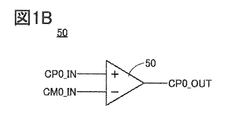
- FIG. 1B is a diagram showing a symbol of the comparator.
- FIG. 1C is a diagram illustrating a configuration example of a comparator.
- FIG. 2A is a diagram showing a symbol of an amplifier.
- 2B and 2C are circuit diagrams showing configuration examples of the amplifier.
- 3A, 3B, 3C, 3D, and 3E are timing charts showing potential fluctuations of the secondary battery and the semiconductor device.
- FIG. 4 is a cross-sectional view showing a configuration example of a semiconductor device.
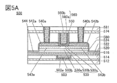
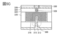
- 5A, 5B, and 5C are cross-sectional views illustrating structural examples of transistors.
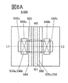
- FIG. 6A is a top view illustrating a structural example of a transistor.
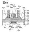
- FIG. 6B and 6C are cross-sectional views illustrating a structural example of a transistor.
- FIG. 7A is a top view illustrating a structural example of a transistor.
- 7B and 7C are cross-sectional views illustrating a structural example of a transistor.
- FIG. 8A is a top view illustrating a structural example of a transistor.
- 8B and 8C are cross-sectional views illustrating a structural example of a transistor.
- FIG. 9A is a top view illustrating a structural example of a transistor.
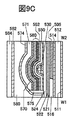
- 9B and 9C are cross-sectional views illustrating a structural example of a transistor.
- FIG. 10A is a top view illustrating a structural example of a transistor.
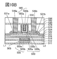
- 10B and 10C are cross-sectional views illustrating a structural example of a transistor.
- FIG. 10A is a top view illustrating a structural example of a transistor.
- 10B and 10C are cross-sectional views illustrating a structural example of a transistor.
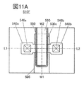
- FIG. 11A is a top view illustrating a structural example of a transistor.
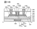
- 11B and 11C are cross-sectional views illustrating a structural example of a transistor.
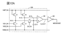
- FIG. 12A is a diagram showing a circuit measured using an oscilloscope.
- FIG. 12B is a diagram showing a result of measurement using an oscilloscope.
- film and the term “layer” can be interchanged with each other.
- conductive layer to the term “conductive film”.
- insulating film to the term “insulating layer”.
- gate electrode on the gate insulating layer does not exclude one including another component between the gate insulating layer and the gate electrode.
- the term “electrically connected” includes the case where they are connected through “an object having some electrical action”.
- the “object having some kind of electrical action” is not particularly limited as long as it can transfer an electric signal between the connection targets.
- “things having some kind of electrical action” include electrodes and wirings, switching elements such as transistors, resistance elements, inductors, capacitance elements, and other elements having various functions.
- the term “voltage” often refers to a potential difference between a certain potential and a reference potential (eg, a ground potential). Therefore, the voltage and the potential difference can be rephrased.
- a transistor is an element having at least three terminals including a gate, a drain, and a source.
- a channel formation region is provided between the drain (drain terminal, drain region, or drain electrode) and the source (source terminal, source region, or source electrode), and the source and drain are connected via the channel formation region. A current can be passed between them.
- a channel formation region refers to a region in which a current mainly flows.
- the functions of the source and the drain may be switched when a transistor of different polarity is used or when the direction of current changes in circuit operation. Therefore, in this specification and the like, the terms “source” and “drain” can be replaced with each other.
- off-state current refers to drain current when a transistor is in an off state (also referred to as a non-conducting state or a blocking state).
- the off state is a state in which the gate voltage Vgs with respect to the source is lower than the threshold voltage Vth in the n-channel transistor, and the gate voltage Vgs with respect to the source in the p-channel transistor is the threshold voltage Vth.
- the state is higher than the voltage Vth. That is, the off-state current of the n-channel transistor may be a drain current when the gate voltage Vgs with respect to the source is lower than the threshold voltage Vth.
- off-state current may refer to the source current when the transistor is off. Further, it may be referred to as a leak current in the same meaning as the off current. In this specification and the like, off-state current may refer to current flowing between a source and a drain when a transistor is off.
- a metal oxide is a metal oxide in a broad sense. Metal oxides are classified into oxide insulators, oxide conductors (including transparent oxide conductors), oxide semiconductors, and the like.
- the metal oxide when a metal oxide is used for a channel formation region of a transistor, the metal oxide may be referred to as an oxide semiconductor. That is, when the metal oxide has at least one of an amplifying action, a rectifying action, and a switching action, the metal oxide can be referred to as a metal oxide semiconductor. That is, a transistor including a metal oxide in a channel formation region can be referred to as an “oxide semiconductor transistor” or an “OS transistor”. Similarly, the above-described "transistor using an oxide semiconductor” is a transistor including a metal oxide in a channel formation region.
- a metal oxide containing nitrogen may also be referred to as a metal oxide. Further, the metal oxide containing nitrogen may be referred to as a metal oxynitride. Details of the metal oxide will be described later.
- a semiconductor device configured such that, in a secondary battery which is being charged and discharged, a potential between a positive electrode and a negative electrode of the secondary battery is sampled (acquired) at predetermined intervals, and the sampled potential and the positive electrode after sampling are sampled.
- a potential between a positive electrode and a negative electrode of the secondary battery is sampled (acquired) at predetermined intervals, and the sampled potential and the positive electrode after sampling are sampled.
- it has a function of detecting an instantaneous potential fluctuation (here, the potential drops) due to a micro short circuit.
- the semiconductor device can cope with potential fluctuation of the secondary battery during charging and discharging, and can be operated using the potential between the positive electrode and the negative electrode of the secondary battery.
- FIG. 1A is a circuit diagram showing a configuration example of the semiconductor device 100.
- the semiconductor device 100 includes transistors 11 to 15, a capacitor C11, and a comparator 50. Note that in the drawings described in this specification and the like, main signal flows are indicated by arrows or lines, and power supply lines and the like may be omitted.
- the semiconductor device 100 includes a wiring VBM_IN supplied with a negative electrode potential VBM of a secondary battery (not shown), a wiring VBP_IN supplied with a positive electrode potential VBP of the secondary battery, and a wiring VB1_IN supplied with a predetermined potential VB1.
- a wiring VB2_IN to which the potential VB2 of the above is supplied a wiring SH_IN to which the sampling signal SH is supplied, and an output terminal S_OUT.
- the predetermined potential VB1 is higher than the predetermined potential VB2, and the predetermined potential VB2 is higher than the negative potential VBM.
- the positive electrode potential VBP may be a high power supply potential
- the negative electrode potential VBM may be a low power supply potential
- the negative electrode potential VBM may be called a reference potential.
- the transistors 11 to 15 are n-channel transistors. Although an example in which the semiconductor device 100 is formed using an n-channel transistor is described in this specification and the like, a p-channel transistor may be used. Since a person skilled in the art can easily understand that a transistor is changed to a p-channel type from a circuit diagram configured by using an n-channel type transistor, description thereof will be omitted.
- one of a source and a drain of the transistor 11 is electrically connected to the wiring VBM_IN, and the other of the source and the drain of the transistor 11 is one of the source and the drain of the transistor 12 and the source or the drain of the transistor 15.
- the transistor 11 is electrically connected to one of the drains, the gate of the transistor 11 is electrically connected to the wiring VB1_IN, and the other of the source and the drain of the transistor 12 and the gate of the transistor 12 are electrically connected to the wiring VBP_IN.
- One of a source and a drain of the transistor 13 is electrically connected to the wiring VBM_IN, and the other of the source and the drain of the transistor 13 is one of the source and the drain of the transistor 14 and the inverting input terminal of the comparator 50 (in FIG. , "-"),
- the gate of the transistor 13 is electrically connected to the wiring VB2_IN, and the other of the source and the drain of the transistor 14 and the gate of the transistor 14 are electrically connected to the wiring VBP_IN. Connected to each other.
- the other of the source and the drain of the transistor 15 is electrically connected to one terminal of the capacitor C11 and the non-inverting input terminal of the comparator 50 (denoted as “+” in FIG. 1A), and The gate is electrically connected to the wiring SH_IN, the other terminal of the capacitor C11 is electrically connected to the wiring VBM_IN, and the output terminal of the comparator 50 is electrically connected to the output terminal S_OUT.
- the other terminal of the capacitor C11 may be electrically connected to a wiring other than the wiring VBM_IN as long as the wiring is supplied with a predetermined potential.
- a connection portion where the other of the source and the drain of the transistor 11, the one of the source and the drain of the transistor 12, and the one of the source and the drain of the transistor 15 are electrically connected is referred to as a node N11.
- the other of the source and the drain of 13, the one of the source and the drain of the transistor 14, and the inverting input terminal of the comparator 50 are electrically connected to each other, which is referred to as a node N12.
- a connection portion in which the other terminal, one terminal of the capacitive element C11, and the non-inverting input terminal of the comparator 50 are electrically connected is referred to as a node N13.
- the transistor 11 and the transistor 12 form a first source follower
- the transistor 13 and the transistor 14 form a second source follower. That is, the gate of the transistor 11 corresponds to the input of the first source follower, and the first source follower outputs the potential to the node N11.
- the gate of the transistor 13 corresponds to the input of the second source follower, and the second source follower outputs the potential to the node N12.
- the comparator 50 has a non-inverting input terminal, an inverting input terminal, and an output terminal.
- the comparator 50 has a function of amplifying the potential difference input to the non-inverting input terminal and the inverting input terminal.
- the comparator 50 amplifies and outputs in the direction of the high power supply potential, and the potential input to the non-inverting input terminal is inverted. If it is smaller than the potential input to the input terminal, it is amplified in the low power supply potential direction and output.
- the symbol of the comparator 50 is shown in FIG. 1B.
- the non-inverting input terminal of the comparator 50 is referred to as an input terminal CP0_IN
- the inverting input terminal is referred to as an input terminal CM0_IN
- the output terminal is referred to as an output terminal CP0_OUT.
- the comparator 50 has one or a plurality of amplifiers 51 connected in series. A configuration example in which the comparator 50 has a plurality of amplifiers 51 is shown in FIG. 1C.
- the amplifier 51 has a non-inverting input terminal, an inverting input terminal, a non-inverting output terminal, and an inverting output terminal.
- the symbol of the amplifier 51 is shown in FIG. 2A.
- the non-inverting input terminal of the amplifier 51 is called an input terminal CP1_IN
- the inverting input terminal is called an input terminal CM1_IN
- the non-inverting output terminal is called an output terminal CP1_OUT
- an inverting output is called.
- the terminal is called an output terminal CM1_OUT.
- the input terminal CP0_IN is electrically connected to the input terminal CP1_IN of the first amplifier 51 (see FIG. 2A), and the input terminal CM0_IN is electrically connected to the input terminal CM1_IN of the first amplifier 51.
- the output terminal CP1_OUT of the first amplifier 51 is electrically connected to the input terminal CP1_IN of the second amplifier 51, and the output terminal CM1_OUT of the first amplifier 51 is the input terminal CM1_IN of the second amplifier 51. It shows a state of being electrically connected with.
- the output terminal CP1_OUT of the last amplifier 51 among the plurality of amplifiers 51 is electrically connected to the output terminal CP0_OUT.
- the number of the amplifiers 51 can be determined by comparing the amplification factor required for the comparator 50 with the amplification factor of one amplifier 51.
- FIG. 2B is a circuit diagram showing an example in which the amplifier 51 is configured by using an n-channel type transistor.
- the amplifier 51 includes transistors 21 to 25.
- the transistors 21 to 25 are n-channel transistors.
- the amplifier 51 has a wiring VBM_IN to which the negative electrode potential VBM of the secondary battery is supplied, a wiring VBP_IN to which the positive electrode potential VBP of the secondary battery is supplied, a wiring VB3_IN to which a predetermined potential VB3 is supplied, an input terminal CP1_IN, and an input. It has a terminal CM1_IN, an output terminal CP1_OUT, and an output terminal CM1_OUT.
- the predetermined potential VB3 is higher than the negative potential VBM, and in the amplifier 51, the positive potential VBP is a high power supply potential and the negative potential VBM is a low power supply potential.
- one of a source and a drain of the transistor 21 is electrically connected to the wiring VBM_IN, and the other of the source and the drain of the transistor 21 is one of the source and the drain of the transistor 22 and the source or the drain of the transistor 24.
- the gate of the transistor 21 is electrically connected to the wiring VB3_IN.
- the other of the source and the drain of the transistor 22 is electrically connected to one of the source and the drain of the transistor 23 and the output terminal CM1_OUT, and the other of the source and the drain of the transistor 23 and the gate of the transistor 23 are connected to the wiring VBP_IN.
- the gate of the transistor 22 is electrically connected to the input terminal CP1_IN.
- the other of the source and the drain of the transistor 24 is electrically connected to one of the source and the drain of the transistor 25 and the output terminal CP1_OUT, and the other of the source and the drain of the transistor 25 and the gate of the transistor 25 are connected to the wiring VBP_IN.
- the gate of the transistor 24 is electrically connected to the input terminal CM1_IN.
- FIG. 2C is a circuit diagram showing a configuration example of the amplifier 51 different from that in FIG. 2B.
- the amplifier 51 illustrated in FIG. 2C includes a resistance element R11, a resistance element R12, a transistor 21, a transistor 22, a transistor 24, and transistors 26 to 29.
- the transistor 21, the transistor 22, the transistor 24, and the transistors 26 to 29 are n-channel transistors.
- one of a source and a drain of the transistor 21 is electrically connected to the wiring VBM_IN, and the other of the source and the drain of the transistor 21 is one of the source and the drain of the transistor 22 and the transistor 24. Is electrically connected to one of a source and a drain of the transistor 21.
- a gate of the transistor 21 is electrically connected to the wiring VB3_IN, a gate of the transistor 26, and a gate of the transistor 28.
- the other of the source and the drain of the transistor 22 is electrically connected to one terminal of the resistor element R11 and the gate of the transistor 29, and the other terminal of the resistor element R11 is electrically connected to the wiring VBP_IN.
- the gate of 22 is electrically connected to the input terminal CP1_IN.
- the other of the source and the drain of the transistor 24 is electrically connected to one terminal of the resistance element R12 and the gate of the transistor 27, and the other terminal of the resistance element R12 is electrically connected to the wiring VBP_IN.
- the gate of 24 is electrically connected to the input terminal CM1_IN.
- one of a source and a drain of the transistor 26 is electrically connected to the wiring VBM_IN, and the other of the source and the drain of the transistor 26 is electrically connected to one of the source and the drain of the transistor 27 and the output terminal CP1_OUT.
- the other of the source and the drain of the transistor 27 is electrically connected to the wiring VBP_IN.
- One of a source and a drain of the transistor 28 is electrically connected to the wiring VBM_IN, and the other of the source and the drain of the transistor 28 is electrically connected to one of the source and the drain of the transistor 29 and the output terminal CM1_OUT.
- the other of the source and the drain of the transistor 29 is electrically connected to the wiring VBP_IN.
- ⁇ Operation example of semiconductor device> 3A to 3E are timing charts showing potential fluctuations of the secondary battery and the semiconductor device when the secondary battery is being charged.
- the vertical axis represents potential and the horizontal axis represents time. Note that in FIGS. 3A to 3E, the horizontal axis is common (indicates the same time at the same position).
- the same wiring, the same terminal, or the potential of the same node may be illustrated in a plurality of drawings for reference.
- 3A to 3E show potential fluctuations of the secondary battery and the semiconductor device in the secondary battery which is being charged, divided into periods D11 to D13.
- the period D11 charging of the secondary battery is started and the potential of the wiring, the terminal, or the node is set to a predetermined potential. Further, the potential between the positive electrode and the negative electrode of the secondary battery (more accurately, the potential related to the potential between the positive electrode and the negative electrode) is sampled at every predetermined time.
- a micro short circuit occurs in the period D12, and a period D13 is the charging period after the micro short circuit.
- a secondary battery in which the potential between the positive electrode and the negative electrode fluctuates due to charging and discharging is assumed, but it can also be applied to a secondary battery in which the potential between the positive electrode and the negative electrode does not fluctuate (or decreases) due to charging and discharging. ..
- Examples of the secondary battery in which the potential between the positive electrode and the negative electrode fluctuates due to charging / discharging are lithium ion batteries, and particularly lithium ion batteries during constant current charging are mentioned.
- FIG. 3A shows that the positive electrode potential VBP of the secondary battery rises from the initial potential VD1 when charging is started in the period D11.
- the positive electrode potential VBP (potential between positive and negative electrodes) with respect to the negative electrode potential VBM of the secondary battery increases.
- the positive electrode potential VBP instantaneously drops.
- the micro short circuit ends, the positive electrode potential VBP rises as in the period D11.
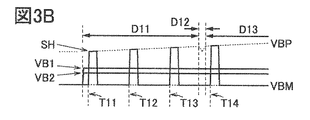
- FIG. 3B shows the states of the predetermined potential VB1, the predetermined potential VB2, and the sampling signal SH.
- the potential VB1 and the potential VB2 are applied, and the sampling signal SH becomes high level every predetermined time.
- the high level of the sampling signal SH is represented by using the positive electrode potential VBP
- the low level of the sampling signal SH is represented by using the negative electrode potential VBM.
- the sampling signal SH becomes high level from time T11 to time T14.
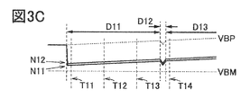
- FIG. 3C the states of the node N11 and the node N12 are shown.
- the potential VB1 and the potential VB2 are applied in the period D11, the potentials of the node N11 and the node N12 are determined. Since the potential VB1 is higher than the potential VB2, the potential of the node N11 is lower than the potential of the node N12, and the potentials of the node N11 and the node N12 also rise as the positive potential VBP rises.
- a micro short circuit occurs in the period D12 and the positive electrode potential VBP instantaneously drops, the potentials of the nodes N11 and N12 also instantaneously drop.
- FIG. 3D the states of the node N12 and the node N13 are shown.
- the potential of the node N13 is set to the potential of the node N11 at that time when the sampling signal SH goes high. Therefore, the potential of the node N13 is lower than the potential of the node N12 and rises stepwise.
- the sampling signal SH is at low level, the potential of the node N13 is not affected by the potential of the node N11. Therefore, even if a micro short circuit occurs in the period D12 and the positive electrode potential VBP momentarily drops, the potential of the node N13 does not change. As a result, in the period D12, the potential of the node N13 becomes higher than the potential of the node N12.
- FIG. 3E the appearance of the output terminal S_OUT is shown.
- the potential of the output terminal S_OUT in the periods D11 and D13, since the potential of the node N13 is lower than the potential of the node N12, the potential of the output terminal S_OUT is the negative potential VBM (low level).
- the potential of the node N13 becomes higher than the potential of the node N12, so that the potential of the output terminal S_OUT becomes the positive potential VBP (high level).
- the semiconductor device 100 outputs the negative electrode potential VBM from the output terminal S_OUT during the period D11 and the period D13 in which the micro short circuit does not occur, and outputs the positive electrode potential VBP from the output terminal S_OUT when the micro short circuit occurs.
- the semiconductor device 100 samples the potential of the node N11 related to the potential between the positive electrode and the negative electrode of the secondary battery before the occurrence of the micro short circuit, so that even if the potential between the positive electrode and the negative electrode is slightly reduced, Micro shorts can be detected.
- the semiconductor device 100 has a function as an abnormality detection device that detects a micro short circuit in the secondary battery.
- Transistor configuring semiconductor device As the transistors 11 to 15 included in the semiconductor device 100 and the transistor included in the comparator 50, a transistor including a metal oxide in a channel formation region (OS transistor) can be used.
- OS transistor a transistor including a metal oxide in a channel formation region
- the OS transistor has features such that the off-state current is extremely small, a high voltage can be applied between the source and the drain, and the OS transistor is a thin film transistor and can be stacked.
- off-state current refers to drain current when the transistor is in an off state. Since the band gap of the oxide semiconductor is 2.5 eV or more, preferably 3.0 eV or more, the OS transistor has a feature that leak current due to thermal excitation is small and off-state current is extremely small.
- the OS transistor can have an off-state current per channel width of 1 ⁇ m of 100 zA / ⁇ m or less, 10 zA / ⁇ m or less, 1 zA / ⁇ m or less, or 10 yA / ⁇ m or less, for example.
- the OS transistor is particularly suitable for the transistor 15 because it has a characteristic of extremely low off-state current.
- the leak current from the capacitor C11 can be suppressed low and the potential of the node N13 can be held accurately. That is, the semiconductor device 100 can accurately detect the micro short even when the potential fluctuation between the positive electrode and the negative electrode of the secondary battery due to the micro short is small.
- the leakage current from the capacitor C11 can be suppressed low and the potential of the node N13 can be held long. That is, the interval for sampling the potential between the positive electrode and the negative electrode of the secondary battery can be increased, and the semiconductor device 100 can be a semiconductor device with low power consumption and less susceptible to noise or the like. For example, the timing at which the semiconductor device 100 samples the potential between the positive electrode and the negative electrode and the probability that a micro short circuit occurs at the same time can be reduced.
- the OS transistor is characterized in that the off current is unlikely to increase even in a high temperature environment and the ratio of on current to off current is large even in a high temperature environment.
- the reliability of the semiconductor device 100 can be improved by configuring the semiconductor device 100 using an OS transistor.
- the metal oxide used for the channel formation region of the OS transistor is preferably an oxide semiconductor containing at least one of indium (In) and zinc (Zn).
- an oxide semiconductor an In-M-Zn oxide (the element M is, for example, Al, Ga, Y, or Sn) is typical.
- the oxide semiconductor can be i-type (intrinsic) or substantially i-type.
- Such an oxide semiconductor can be referred to as a highly purified oxide semiconductor. Note that details of the OS transistor will be described in Embodiments 2 and 3.
- the OS transistor is a thin film transistor, it can be stacked.
- the OS transistor can be provided over a circuit including a Si transistor formed over a single crystal silicon substrate. Therefore, the chip area of the semiconductor device 100 can be reduced.
- transistors other than the OS transistor may be used as the transistors 11 to 15 included in the semiconductor device 100 and the transistors included in the comparator 50.
- a transistor including a semiconductor with a wide bandgap in a channel formation region may be used.
- the semiconductor with a large band gap may refer to a semiconductor with a band gap of 2.2 eV or more, and examples thereof include silicon carbide, gallium nitride, and diamond.
- the semiconductor device 100 samples the potential related to the positive-negative potential of the secondary battery and compares the sampled potential with the potential related to the positive-negative potential after sampling, thereby It is possible to detect a momentary and small potential fluctuation due to a short circuit. That is, it is possible to deal with the potential fluctuation of the secondary battery during charging or the like.
- the sampled potential can be accurately held and even when the potential fluctuation is small, it can be detected.
- the sampling interval can be lengthened.
- the semiconductor device 100 can be operated using the potential between the positive electrode and the negative electrode of the secondary battery by lowering the sampling potential by using the first source follower and the second source follower. Since it is not necessary to provide a potential other than the negative electrode potential and the positive electrode potential of the secondary battery as the power source potential, the power consumption of the semiconductor device 100 can be reduced.
- Embodiment 2 In this embodiment, an example of a structure of an OS transistor which can be used for the semiconductor device 100 described in any of the above embodiments will be described. Note that the OS transistor is a thin film transistor and can be provided by stacking. Therefore, in this embodiment, a structural example of a semiconductor device in which an OS transistor is provided above a Si transistor formed over a single crystal silicon substrate is described. To do.
- the semiconductor device illustrated in FIG. 4 includes a transistor 300, a transistor 500, and a capacitor 600.
- 5A is a cross-sectional view of the transistor 500 in the channel length direction
- FIG. 5B is a cross-sectional view of the transistor 500 in the channel width direction
- FIG. 5C is a cross-sectional view of the transistor 300 in the channel width direction.
- the transistor 500 is a transistor including a metal oxide in a channel formation region (OS transistor). Since the transistor 500 has a feature that the off-state current is extremely small, in the above embodiment, by using the transistor 500 in the semiconductor device 100, even if the potential variation between the positive electrode and the negative electrode of the secondary battery due to a micro short circuit is small, the semiconductor The device 100 can detect a micro short.
- OS transistor metal oxide in a channel formation region
- the semiconductor device described in this embodiment includes a transistor 300, a transistor 500, and a capacitor 600 as illustrated in FIG.
- the transistor 500 is provided above the transistor 300
- the capacitor 600 is provided above the transistor 300 and the transistor 500.
- the transistor 300 is provided over the substrate 311, and includes a conductor 316, an insulator 315, a semiconductor region 313 formed of part of the substrate 311, a low resistance region 314a functioning as a source region or a drain region, and a low resistance region 314b.
- a conductor 316 includes a conductor 316, an insulator 315, a semiconductor region 313 formed of part of the substrate 311, a low resistance region 314a functioning as a source region or a drain region, and a low resistance region 314b.
- the transistor 300 As shown in FIG. 5C, in the transistor 300, the upper surface of the semiconductor region 313 and the side surface in the channel width direction are covered with the conductor 316 with the insulator 315 interposed therebetween. As described above, when the transistor 300 is a Fin type, the effective channel width is increased, so that the on-state characteristics of the transistor 300 can be improved. Further, since the electric field contribution of the gate electrode can be increased, the off characteristics of the transistor 300 can be improved.
- the transistor 300 may be either a p-channel type or an n-channel type.
- a region of the semiconductor region 313 in which a channel is formed, a region in the vicinity thereof, a low-resistance region 314a serving as a source region or a drain region, a low-resistance region 314b, or the like preferably contains a semiconductor such as a silicon-based semiconductor. It preferably includes crystalline silicon. Alternatively, a material including Ge (germanium), SiGe (silicon germanium), GaAs (gallium arsenide), GaAlAs (gallium aluminum arsenide), or the like may be used. A configuration may be used in which silicon is used, in which the effective mass is controlled by applying stress to the crystal lattice and changing the lattice spacing. Alternatively, the transistor 300 may be a HEMT (High Electron Mobility Transistor) by using GaAs and GaAlAs.
- HEMT High Electron Mobility Transistor
- the low-resistance region 314a and the low-resistance region 314b impart an n-type conductivity imparting element such as arsenic or phosphorus, or a p-type conductivity imparting boron, in addition to the semiconductor material applied to the semiconductor region 313. Including the element to do.
- the conductor 316 functioning as a gate electrode is a semiconductor material such as silicon, a metal material, or an alloy containing an element imparting n-type conductivity such as arsenic or phosphorus, or an element imparting p-type conductivity such as boron. Materials or conductive materials such as metal oxide materials can be used.
- Vth of the transistor can be adjusted by changing the material of the conductor.
- a material such as titanium nitride or tantalum nitride for the conductor.
- a metal material such as tungsten or aluminum, and it is particularly preferable to use tungsten in terms of heat resistance.
- transistor 300 illustrated in FIGS. 4A and 4B is an example, and the structure thereof is not limited, and an appropriate transistor may be used depending on a circuit configuration or a driving method.
- An insulator 320, an insulator 322, an insulator 324, and an insulator 326 are sequentially stacked to cover the transistor 300.
- the insulator 320, the insulator 322, the insulator 324, and the insulator 326 for example, silicon oxide, silicon oxynitride, silicon nitride oxide, silicon nitride, aluminum oxide, aluminum oxynitride, aluminum nitride oxide, aluminum nitride, or the like is used. Good.
- the insulator 322 may have a function as a planarization film which planarizes a step generated by the transistor 300 or the like provided below the insulator 322.
- the upper surface of the insulator 322 may be flattened by a flattening treatment using a chemical mechanical polishing (CMP) method or the like in order to improve flatness.
- CMP chemical mechanical polishing
- the insulator 324 it is preferable to use a film having a barrier property such that hydrogen and impurities do not diffuse from the substrate 311, the transistor 300, or the like to a region where the transistor 500 is provided.
- a film having a barrier property against hydrogen for example, silicon nitride formed by a CVD method can be used.
- silicon nitride formed by a CVD method when hydrogen is diffused into a semiconductor element including an oxide semiconductor, such as the transistor 500, characteristics of the semiconductor element may be deteriorated in some cases. Therefore, it is preferable to use a film which suppresses diffusion of hydrogen between the transistor 500 and the transistor 300.
- the film that suppresses hydrogen diffusion is a film in which the amount of released hydrogen is small.
- the desorption amount of hydrogen can be analyzed using, for example, the temperature programmed desorption gas analysis (TDS analysis) method.
- TDS analysis the desorption amount of hydrogen in the insulator 324 is calculated by converting the desorption amount converted into hydrogen atoms into the area of the insulator 324 when the surface temperature of the film is in the range of 50 ° C to 500 ° C. Therefore, it may be 10 ⁇ 10 15 atoms / cm 2 or less, preferably 5 ⁇ 10 15 atoms / cm 2 or less.
- the insulator 326 preferably has a lower dielectric constant than the insulator 324.
- the dielectric constant of the insulator 326 is preferably less than 4, and more preferably less than 3.
- the relative dielectric constant of the insulator 326 is preferably 0.7 times or less, and more preferably 0.6 times or less that of the insulator 324.
- the insulator 320, the insulator 322, the insulator 324, and the insulator 326 are embedded with a conductor 328 which is connected to the capacitor 600 or the transistor 500, a conductor 330, and the like.
- the conductor 328 and the conductor 330 have a function as a plug or a wiring.
- a conductor having a function as a plug or a wiring may have a plurality of structures collectively given the same reference numeral. In this specification and the like, the wiring and the plug connected to the wiring may be integrated. That is, part of the conductor may function as a wiring, and part of the conductor may function as a plug.
- a conductive material such as a metal material, an alloy material, a metal nitride material, or a metal oxide material is formed in a single layer or stacked layers.
- a high melting point material such as tungsten or molybdenum that has both heat resistance and conductivity, and it is particularly preferable to use tungsten.
- it is preferably formed of a low resistance conductive material such as aluminum or copper. Wiring resistance can be reduced by using a low-resistance conductive material.
- a wiring layer may be provided over the insulator 326 and the conductor 330.
- an insulator 350, an insulator 352, and an insulator 354 are sequentially stacked and provided.
- a conductor 356 is formed over the insulator 350, the insulator 352, and the insulator 354.
- the conductor 356 has a function as a plug connected to the transistor 300 or a wiring. Note that the conductor 356 can be provided using a material similar to that of the conductor 328 and the conductor 330.
- the insulator 350 is preferably an insulator having a barrier property against hydrogen similarly to the insulator 324.
- the conductor 356 preferably contains a conductor having a barrier property against hydrogen.
- a conductor having a hydrogen barrier property is formed in an opening portion of the insulator 350 having a hydrogen barrier property.
- tantalum nitride or the like is preferably used as the conductor having a barrier property against hydrogen.
- tantalum nitride or the like is preferably used as the conductor having a barrier property against hydrogen.
- tantalum nitride and tungsten having high conductivity diffusion of hydrogen from the transistor 300 can be suppressed while maintaining conductivity as a wiring.
- the tantalum nitride layer having a barrier property against hydrogen be in contact with the insulator 350 having a barrier property against hydrogen.
- a wiring layer may be provided over the insulator 354 and the conductor 356.
- an insulator 360, an insulator 362, and an insulator 364 are sequentially stacked and provided.
- a conductor 366 is formed over the insulator 360, the insulator 362, and the insulator 364.
- the conductor 366 has a function as a plug or a wiring. Note that the conductor 366 can be provided using a material similar to that of the conductor 328 and the conductor 330.
- the insulator 360 like the insulator 324, an insulator having a barrier property against hydrogen is preferably used.
- the conductor 366 preferably contains a conductor having a barrier property against hydrogen.
- a conductor having a hydrogen barrier property is formed in the opening of the insulator 360 having a hydrogen barrier property.
- a wiring layer may be provided over the insulator 364 and the conductor 366.
- an insulator 370, an insulator 372, and an insulator 374 are sequentially stacked and provided.
- a conductor 376 is formed over the insulator 370, the insulator 372, and the insulator 374.
- the conductor 376 has a function as a plug or a wiring. Note that the conductor 376 can be provided using a material similar to that of the conductor 328 and the conductor 330.
- the conductor 376 preferably includes a conductor having a barrier property against hydrogen.
- a conductor having a hydrogen barrier property is formed in the opening of the insulator 370 having a hydrogen barrier property.
- a wiring layer may be provided over the insulator 374 and the conductor 376.
- an insulator 380, an insulator 382, and an insulator 384 are sequentially stacked and provided.
- a conductor 386 is formed over the insulator 380, the insulator 382, and the insulator 384.
- the conductor 386 has a function as a plug or a wiring. Note that the conductor 386 can be provided using a material similar to that of the conductor 328 and the conductor 330.
- the insulator 380 is preferably an insulator having a barrier property against hydrogen, like the insulator 324.
- the conductor 386 preferably contains a conductor having a barrier property against hydrogen.
- a conductor having a barrier property against hydrogen is formed in the opening portion of the insulator 380 having a barrier property against hydrogen.
- the semiconductor device has been described above, the semiconductor device according to this embodiment It is not limited to this.
- the number of wiring layers similar to the wiring layer including the conductor 356 may be three or less, or the number of wiring layers similar to the wiring layer including the conductor 356 may be five or more.
- An insulator 510, an insulator 512, an insulator 514, and an insulator 516 are sequentially stacked over the insulator 384.
- Any of the insulator 510, the insulator 512, the insulator 514, and the insulator 516 is preferably formed using a substance having a barrier property against oxygen and hydrogen.
- insulator 510 and the insulator 514 for example, a film having a barrier property in which hydrogen and impurities do not diffuse from the substrate 311 or a region where the transistor 300 is provided to a region where the transistor 500 is provided is used. Is preferred. Therefore, a material similar to that of the insulator 324 can be used.
- silicon nitride formed by a CVD method can be used as an example of a film having a barrier property against hydrogen.
- silicon nitride formed by a CVD method when hydrogen is diffused into a semiconductor element including an oxide semiconductor, such as the transistor 500, characteristics of the semiconductor element may be deteriorated in some cases. Therefore, it is preferable to use a film which suppresses diffusion of hydrogen between the transistor 500 and the transistor 300.
- the film that suppresses hydrogen diffusion is a film in which the amount of released hydrogen is small.
- a metal oxide such as aluminum oxide, hafnium oxide, or tantalum oxide is preferably used for the insulator 510 and the insulator 514.
- aluminum oxide has a high blocking effect of not permeating oxygen and impurities such as hydrogen and moisture, which cause fluctuations in electrical characteristics of a transistor, through the film. Therefore, aluminum oxide can prevent impurities such as hydrogen and moisture from entering the transistor 500 during and after the manufacturing process of the transistor. Further, release of oxygen from the oxide included in the transistor 500 can be suppressed. Therefore, it is suitable to be used as a protective film for the transistor 500.
- the same material as that of the insulator 320 can be used for the insulator 512 and the insulator 516. Further, by using a material having a relatively low dielectric constant as the interlayer film, it is possible to reduce the parasitic capacitance generated between the wirings.
- a silicon oxide film, a silicon oxynitride film, or the like can be used as the insulator 512 and the insulator 516.
- a conductor 518, a conductor (conductor 503) included in the transistor 500, and the like are embedded in the insulator 510, the insulator 512, the insulator 514, and the insulator 516.
- the conductor 518 has a function of a plug connected to the capacitor 600 or the transistor 300, or a wiring.
- the conductor 518 can be provided using a material similar to that of the conductor 328 and the conductor 330.
- the conductor 510 in a region which is in contact with the insulator 510 and the insulator 514 is preferably a conductor having a barrier property against oxygen, hydrogen, and water.
- the transistor 300 and the transistor 500 can be separated by a layer having a barrier property against oxygen, hydrogen, and water, and diffusion of hydrogen from the transistor 300 to the transistor 500 can be suppressed.
- the transistor 500 is provided above the insulator 516.
- the transistor 500 includes a conductor 503 arranged so as to be embedded in an insulator 514 and an insulator 516, and an insulator 520 arranged over the insulator 516 and the conductor 503.
- the insulator 544 is preferably provided between the oxide 530a, the oxide 530b, the conductor 542a, and the conductor 542b, and the insulator 580.
- the conductor 560 includes a conductor 560a provided inside the insulator 550 and a conductor 560b provided so as to be embedded inside the conductor 560a. It is preferable to have.
- the insulator 574 is preferably provided over the insulator 580, the conductor 560, and the insulator 550.
- the oxide 530a, the oxide 530b, and the oxide 530c may be collectively referred to as the oxide 530.
- the conductor 542a and the conductor 542b may be collectively referred to as a conductor 542.
- the transistor 500 has a structure in which three layers of the oxide 530a, the oxide 530b, and the oxide 530c are stacked in the region where the channel is formed and in the vicinity thereof, the present invention is not limited to this. Not a thing. For example, a single layer of the oxide 530b, a two-layer structure of the oxide 530b and the oxide 530a, a two-layer structure of the oxide 530b and the oxide 530c, or a stacked structure of four or more layers may be provided. Further, in the transistor 500, the conductor 560 is shown as a stacked structure of two layers, but the present invention is not limited to this. For example, the conductor 560 may have a single-layer structure or a stacked structure including three or more layers. Further, the transistor 500 illustrated in FIGS. 4, 5A, and 5B is an example, and the structure is not limited thereto, and an appropriate transistor may be used depending on a circuit configuration or a driving method.
- the conductor 560 functions as a gate electrode of the transistor, and the conductors 542a and 542b function as a source electrode or a drain electrode, respectively.
- the conductor 560 is formed so as to be embedded in the opening of the insulator 580 and the region between the conductor 542a and the conductor 542b.
- the arrangement of the conductor 560, the conductor 542a, and the conductor 542b is selected in a self-aligned manner with respect to the opening of the insulator 580. That is, in the transistor 500, the gate electrode can be arranged between the source electrode and the drain electrode in a self-aligned manner. Therefore, the conductor 560 can be formed without providing a positioning margin, so that the area occupied by the transistor 500 can be reduced. As a result, miniaturization and high integration of the semiconductor device can be achieved.
- the conductor 560 is formed in a region between the conductor 542a and the conductor 542b in a self-aligned manner, the conductor 560 does not have a region overlapping with the conductor 542a or the conductor 542b. Accordingly, the parasitic capacitance formed between the conductor 560 and the conductors 542a and 542b can be reduced. Therefore, the switching speed of the transistor 500 can be improved and high frequency characteristics can be provided.
- the conductor 560 may function as a first gate (also referred to as a top gate) electrode.
- the conductor 503 may function as a second gate (also referred to as a bottom gate) electrode.
- the Vth of the transistor 500 can be controlled by changing the potential applied to the conductor 503 independently of the potential applied to the conductor 560 without being interlocked.
- Vth of the transistor 500 can be higher than 0 V and off-state current can be reduced. Therefore, applying a negative potential to the conductor 503 can reduce the drain current when the potential applied to the conductor 560 is 0 V, as compared to the case where no potential is applied.
- the conductor 503 is arranged so as to overlap with the oxide 530 and the conductor 560. Thus, when a potential is applied to the conductor 560 and the conductor 503, the electric field generated from the conductor 560 and the electric field generated from the conductor 503 are connected to cover a channel formation region formed in the oxide 530.
- a structure of a transistor which electrically surrounds a channel formation region by an electric field of a first gate electrode and a second gate electrode is referred to as a surrounded channel (S-channel) structure.
- the side surface and the periphery of the oxide 530 which is in contact with the conductors 542a and 542b functioning as a source electrode and a drain electrode are i-type as in the channel formation region. It has characteristics.
- the side surface and the periphery of the oxide 530 which are in contact with the conductors 542a and 542b are in contact with the insulator 544 and thus can be i-type as in the channel formation region.
- I-form can be treated as the same as high-purity intrinsic, which will be described later.
- the S-channel structure disclosed in this specification and the like is different from the Fin structure and the planar structure.
- the conductor 503 has a structure similar to that of the conductor 518.
- the conductor 503a is formed in contact with the inner walls of the openings of the insulator 514 and the insulator 516, and the conductor 503b is formed further inside.
- the insulator 520, the insulator 522, the insulator 524, and the insulator 550 have a function as a gate insulating film.
- the insulator 524 which is in contact with the oxide 530, an insulator containing more oxygen than that in the stoichiometric composition is preferably used. That is, it is preferable that the insulator 524 be formed with an excess oxygen region. By providing such an insulator containing excess oxygen in contact with the oxide 530, oxygen vacancies in the oxide 530 can be reduced and the reliability of the transistor 500 can be improved.
- an oxide material in which part of oxygen is released by heating is preferably used as the insulator having an excess oxygen region.
- the oxide that desorbs oxygen by heating means that the amount of desorbed oxygen in terms of oxygen atoms is 1.0 ⁇ 10 18 atoms / cm 3 or more, preferably 1 or more by TDS (Thermal Desorption Spectroscopy) analysis.
- the oxide film has a density of 0.0 ⁇ 10 19 atoms / cm 3 or more, more preferably 2.0 ⁇ 10 19 atoms / cm 3 or more, or 3.0 ⁇ 10 20 atoms / cm 3 or more.
- the surface temperature of the film during the TDS analysis is preferably 100 ° C. or higher and 700 ° C. or lower, or 100 ° C. or higher and 400 ° C. or lower.
- the insulator 522 preferably has a function of suppressing diffusion of oxygen (eg, oxygen atoms, oxygen molecules) (the oxygen is less likely to permeate).
- oxygen eg, oxygen atoms, oxygen molecules
- the insulator 522 has a function of suppressing diffusion of oxygen and impurities, oxygen included in the oxide 530 does not diffuse to the insulator 520 side, which is preferable. Further, the conductor 503 can be prevented from reacting with the insulator 524 and the oxygen contained in the oxide 530.
- the insulator 522 is, for example, so-called high such as aluminum oxide, hafnium oxide, tantalum oxide, zirconium oxide, lead zirconate titanate (PZT), strontium titanate (SrTiO 3 ) or (Ba, Sr) TiO 3 (BST). It is preferable to use an insulator containing a -k material in a single layer or a laminated layer. As miniaturization and higher integration of transistors progress, problems such as leakage current may occur due to thinning of the gate insulating film. By using a high-k material for the insulator functioning as a gate insulating film, it is possible to reduce the gate potential during transistor operation while maintaining the physical film thickness.
- an insulator containing an oxide of one or both of aluminum and hafnium which is an insulating material having a function of suppressing diffusion of impurities, oxygen, and the like (oxygen does not easily pass through) is preferably used.
- the insulator containing one or both oxides of aluminum and hafnium it is preferable to use aluminum oxide, hafnium oxide, an oxide containing aluminum and hafnium (hafnium aluminate), or the like.
- the insulator 522 is formed using such a material, the insulator 522 suppresses release of oxygen from the oxide 530 and mixture of impurities such as hydrogen from the peripheral portion of the transistor 500 into the oxide 530. Functions as a layer.
- aluminum oxide, bismuth oxide, germanium oxide, niobium oxide, silicon oxide, titanium oxide, tungsten oxide, yttrium oxide, or zirconium oxide may be added to these insulators.
- these insulators may be nitrided. Silicon oxide, silicon oxynitride, or silicon nitride may be stacked over the above insulator and used.
- the insulator 520 is preferably thermally stable.
- silicon oxide and silicon oxynitride are preferable because they are thermally stable.
- an insulator of a high-k material with silicon oxide or silicon oxynitride, an insulator 520 having a stacked structure which is thermally stable and has a high relative dielectric constant can be obtained.
- the insulator 520, the insulator 522, and the insulator 524 may have a stacked structure of two or more layers.
- the laminated structure is not limited to the same material, and may be a laminated structure made of different materials.
- a metal oxide which functions as an oxide semiconductor is preferably used.
- the oxide 530 an In-M-Zn oxide (the element M is aluminum, gallium, yttrium, copper, vanadium, beryllium, boron, titanium, iron, nickel, germanium, zirconium, molybdenum, lanthanum, cerium, neodymium). , Or one or more selected from hafnium, tantalum, tungsten, magnesium, or the like).
- an In—Ga oxide or an In—Zn oxide may be used.
- a metal oxide having a low carrier concentration is preferably used.
- the concentration of impurities in the metal oxide may be lowered and the density of defect states may be lowered.
- low impurity concentration and low defect level density are referred to as high-purity intrinsic or substantially high-purity intrinsic.
- the impurities in the metal oxide include, for example, hydrogen, nitrogen, alkali metals, alkaline earth metals, iron, nickel, silicon and the like.
- hydrogen contained in a metal oxide reacts with oxygen bonded to a metal atom to be water, which may cause oxygen vacancies in the metal oxide. If the channel formation region in the metal oxide contains oxygen vacancies, the transistor might have normally-on characteristics. Further, a defect in which hydrogen is contained in an oxygen vacancy may function as a donor and an electron which is a carrier may be generated. Further, part of hydrogen may be bonded to oxygen which is bonded to a metal atom to generate an electron which is a carrier. Therefore, a transistor including a metal oxide containing a large amount of hydrogen is likely to have normally-on characteristics.
- a defect in which hydrogen is contained in an oxygen vacancy can function as a metal oxide donor.
- the metal oxide may be evaluated not by the donor concentration but by the carrier concentration. Therefore, in this specification and the like, the carrier concentration which is assumed to be a state where no electric field is applied may be used as the parameter of the metal oxide, instead of the donor concentration. That is, the “carrier concentration” described in this specification and the like can be called the “donor concentration” in some cases.
- the hydrogen concentration obtained by secondary ion mass spectrometry is less than 1 ⁇ 10 20 atoms / cm 3 , preferably 1 ⁇ 10 19 atoms / cm 3. It is less than 3 , more preferably less than 5 ⁇ 10 18 atoms / cm 3 , and even more preferably less than 1 ⁇ 10 18 atoms / cm 3 .
- the carrier concentration of the metal oxide in the channel formation region is preferably 1 ⁇ 10 18 cm ⁇ 3 or less and less than 1 ⁇ 10 17 cm ⁇ 3. Is more preferable, less than 1 ⁇ 10 16 cm ⁇ 3 is more preferable, less than 1 ⁇ 10 13 cm ⁇ 3 is still more preferable, and less than 1 ⁇ 10 12 cm ⁇ 3 is further preferable.
- the lower limit of the carrier concentration of the metal oxide in the channel formation region is not particularly limited, but can be set to, for example, 1 ⁇ 10 ⁇ 9 cm ⁇ 3 .
- the conductor 542 (the conductor 542a and the conductor 542b) and the oxide 530 are in contact with each other, so that oxygen in the oxide 530 diffuses into the conductor 542,
- the conductor 542 may be oxidized. Oxidation of the conductor 542 is likely to reduce the conductivity of the conductor 542. Note that diffusion of oxygen in the oxide 530 to the conductor 542 can be restated as absorption of oxygen in the oxide 530 by the conductor 542.
- oxygen in the oxide 530 diffuses into the conductor 542 (the conductor 542a and the conductor 542b), so that the conductor 542a and the oxide 530b are separated from each other and the conductor 542b and the oxide 530b are separated from each other.
- Different layers may be formed between them. Since the different layer contains more oxygen than the conductor 542, it is estimated that the different layer has an insulating property.
- the three-layer structure of the conductor 542, the different layer, and the oxide 530b can be regarded as a three-layer structure including a metal-insulator-semiconductor and a MIS (Metal-Insulator-Semiconductor) structure. In some cases, it may be referred to as a diode junction structure mainly including the MIS structure.
- the different layer is not limited to being formed between the conductor 542 and the oxide 530b; for example, when the different layer is formed between the conductor 542 and the oxide 530c, or It may be formed between the body 542 and the oxide 530b and between the conductor 542 and the oxide 530c.
- a metal oxide having a bandgap of 2 eV or more, preferably 2.5 eV or more is preferably used.
- the oxide 530 includes the oxide 530a below the oxide 530b, so that diffusion of impurities into the oxide 530b from a structure formed below the oxide 530a can be suppressed. Further, by including the oxide 530c over the oxide 530b, diffusion of impurities from the structure formed above the oxide 530c into the oxide 530b can be suppressed.
- the oxide 530 preferably has a stacked structure of a plurality of oxide layers in which the atomic ratio of each metal atom is different.
- the atomic ratio of the element M in the constituent elements is higher than the atomic ratio of the element M in the constituent elements in the metal oxide used for the oxide 530b.
- the atomic ratio of the element M to In is preferably higher than the atomic ratio of the element M to In in the metal oxide used for the oxide 530b.
- the atomic ratio of In to the element M is preferably higher than the atomic ratio of In to the element M in the metal oxide used for the oxide 530a.
- a metal oxide that can be used for the oxide 530a or the oxide 530b can be used.
- the energy of the bottom of the conduction band of the oxide 530a and the oxide 530c is preferably higher than the energy of the bottom of the conduction band of the oxide 530b.
- the electron affinity of the oxide 530a and the oxide 530c be smaller than the electron affinity of the oxide 530b.
- the energy level at the bottom of the conduction band changes gently at the junction of the oxide 530a, the oxide 530b, and the oxide 530c.
- the energy levels at the bottoms of the conduction bands at the junctions of the oxide 530a, the oxide 530b, and the oxide 530c are continuously changed or continuously joined.
- the oxide 530a and the oxide 530b, and the oxide 530b and the oxide 530c have a common element other than oxygen (as a main component), so that a mixed layer with low density of defect states is formed.
- the oxide 530b is an In—Ga—Zn oxide
- an In—Ga—Zn oxide, a Ga—Zn oxide, gallium oxide, or the like may be used as the oxide 530a and the oxide 530c.
- the main path of carriers is the oxide 530b.
- the oxide 530a and the oxide 530c having the above structure, the density of defect states in the interface between the oxide 530a and the oxide 530b and the interface between the oxide 530b and the oxide 530c can be reduced. Therefore, the influence of interface scattering on carrier conduction is reduced and the transistor 500 can obtain high on-state current.
- the conductor 542 (the conductor 542a and the conductor 542b) which functions as a source electrode and a drain electrode is provided over the oxide 530b.
- the conductor 542 aluminum, chromium, copper, silver, gold, platinum, tantalum, nickel, titanium, molybdenum, tungsten, hafnium, vanadium, niobium, manganese, magnesium, zirconium, beryllium, indium, ruthenium, iridium, strontium, It is preferable to use a metal element selected from lanthanum, an alloy containing the above metal element as a component, an alloy in which the above metal elements are combined, or the like.
- tantalum nitride, titanium nitride, tungsten, nitride containing titanium and aluminum, nitride containing tantalum and aluminum, ruthenium oxide, ruthenium nitride, oxide containing strontium and ruthenium, oxide containing lanthanum and nickel, or the like is used.
- tantalum nitride, titanium nitride, nitride containing titanium and aluminum, nitride containing tantalum and aluminum, ruthenium oxide, ruthenium nitride, oxide containing strontium and ruthenium, and oxide containing lanthanum and nickel are difficult to oxidize.
- a conductive material or a material that maintains conductivity even when absorbing oxygen is preferable.
- a region 543 (a region 543a and a region 543b) may be formed as a low-resistance region in the interface of the oxide 530 with the conductor 542 and in the vicinity thereof.
- the region 543a functions as one of the source region and the drain region
- the region 543b functions as the other of the source region and the drain region.
- a channel formation region is formed in a region between the region 543a and the region 543b.
- the oxygen concentration in the region 543 may be reduced. Further, a metal compound layer containing a metal contained in the conductor 542 and a component of the oxide 530 may be formed in the region 543. In such a case, the carrier concentration in the region 543 increases, and the region 543 becomes a low resistance region.
- the insulator 544 is provided so as to cover the conductor 542 and suppresses oxidation of the conductor 542. At this time, the insulator 544 may be provided so as to cover a side surface of the oxide 530 and be in contact with the insulator 524.
- a metal oxide containing one kind or two or more kinds selected from hafnium, aluminum, gallium, yttrium, zirconium, tungsten, titanium, tantalum, nickel, germanium, magnesium, or the like can be used. it can.
- the insulator 544 aluminum oxide, hafnium oxide, an oxide containing hafnium (a hafnium aluminate), or the like, which is an insulator containing an oxide of one or both of aluminum and hafnium.
- hafnium aluminate has higher heat resistance than a hafnium oxide film. Therefore, crystallization is less likely to occur in heat treatment in a later step, which is preferable.
- the insulator 544 is not an essential component when the conductor 542 is a material having oxidation resistance or when the conductivity does not significantly decrease even when oxygen is absorbed. It may be appropriately designed depending on the desired transistor characteristics.
- the insulator 550 functions as a gate insulating film.
- the insulator 550 is preferably arranged in contact with the inside (top surface and side surface) of the oxide 530c.
- the insulator 550 is preferably formed using an insulator from which oxygen is released by heating.
- the amount of released oxygen in terms of oxygen atoms is 1.0 ⁇ 10 18 atoms / cm 3 or more, preferably 1.0 ⁇ 10 19 atoms / cm 3 or more, more preferably 2
- the surface temperature of the film during the TDS analysis is preferably 100 ° C. or higher and 700 ° C. or lower.
- silicon oxide containing excess oxygen, silicon oxynitride, silicon nitride oxide, silicon nitride, silicon oxide containing fluorine, silicon oxide containing carbon, silicon oxide containing carbon and nitrogen, and vacancy Silicon oxide can be used.
- silicon oxide and silicon oxynitride are preferable because they are stable to heat.
- oxygen is effectively supplied from the insulator 550 to the channel formation region of the oxide 530b through the oxide 530c. Can be supplied.
- the concentration of impurities such as water or hydrogen in the insulator 550 is preferably reduced.
- the thickness of the insulator 550 is preferably 1 nm or more and 20 nm or less.
- a metal oxide may be provided between the insulator 550 and the conductor 560 in order to efficiently supply the excess oxygen included in the insulator 550 to the oxide 530.
- the metal oxide preferably suppresses oxygen diffusion from the insulator 550 to the conductor 560.
- diffusion of excess oxygen from the insulator 550 to the conductor 560 is suppressed. That is, a decrease in the amount of excess oxygen supplied to the oxide 530 can be suppressed.
- oxidation of the conductor 560 due to excess oxygen can be suppressed.
- a material that can be used for the insulator 544 may be used.
- the conductor 560 functioning as the first gate electrode has a two-layer structure in FIGS. 5A and 5B, it may have a single-layer structure or a stacked structure of three or more layers.
- the conductor 560a has a function of suppressing diffusion of impurities such as hydrogen atoms, hydrogen molecules, water molecules, nitrogen atoms, nitrogen molecules, nitric oxide molecules (N 2 O, NO, NO 2, etc.), and copper atoms. It is preferable to use materials. Alternatively, it is preferable to use a conductive material having a function of suppressing diffusion of oxygen (eg, at least one of oxygen atoms and oxygen molecules). Since the conductor 560a has a function of suppressing diffusion of oxygen, oxygen contained in the insulator 550 can prevent oxidation of the conductor 560b and decrease in conductivity.
- the conductive material having a function of suppressing diffusion of oxygen for example, tantalum, tantalum nitride, ruthenium, ruthenium oxide, or the like is preferably used.
- the conductor 560b also functions as a wiring, it is preferable to use a conductor having high conductivity.
- a conductor having high conductivity For example, a conductive material containing tungsten, copper, or aluminum as its main component can be used.
- the conductor 560b may have a stacked structure, for example, a stacked structure of titanium or titanium nitride and the above conductive material.
- the insulator 580 is provided over the conductor 542 with the insulator 544 interposed therebetween.
- the insulator 580 preferably has an excess oxygen region.
- silicon oxide and silicon oxynitride are preferable because they are thermally stable.
- silicon oxide and silicon oxide having vacancies are preferable because an excess oxygen region can be easily formed in a later step.
- the insulator 580 preferably has an excess oxygen region. By providing the insulator 580 from which oxygen is released by heating in contact with the oxide 530c, oxygen in the insulator 580 can be efficiently supplied to the oxide 530 through the oxide 530c. Note that the concentration of impurities such as water or hydrogen in the insulator 580 is preferably reduced.
- the opening of the insulator 580 is formed so as to overlap with a region between the conductor 542a and the conductor 542b. Accordingly, the conductor 560 is formed so as to be embedded in the opening of the insulator 580 and the region between the conductor 542a and the conductor 542b.
- the conductor 560 When miniaturizing a semiconductor device, it is required to shorten the gate length, but it is necessary to prevent the conductivity of the conductor 560 from being lowered. Therefore, if the thickness of the conductor 560 is increased, the conductor 560 can have a shape with a high aspect ratio. In this embodiment mode, the conductor 560 is provided so as to be embedded in the opening of the insulator 580; therefore, even if the conductor 560 has a high aspect ratio, the conductor 560 can be formed without being destroyed during the process. You can
- the insulator 574 is preferably provided in contact with the top surface of the insulator 580, the top surface of the conductor 560, and the top surface of the insulator 550.
- an excess oxygen region can be provided in the insulator 550 and the insulator 580. Accordingly, oxygen can be supplied into the oxide 530 from the excess oxygen region.
- insulator 574 a metal oxide containing one kind or two or more kinds selected from hafnium, aluminum, gallium, yttrium, zirconium, tungsten, titanium, tantalum, nickel, germanium, magnesium, or the like is used. You can
- aluminum oxide has a high barrier property and can suppress diffusion of hydrogen and nitrogen even in a thin film of 0.5 nm to 3.0 nm. Therefore, the aluminum oxide film formed by a sputtering method can have a function as a barrier film against impurities such as hydrogen as well as an oxygen supply source.
- an insulator 581 which functions as an interlayer film is preferably provided over the insulator 574.
- the insulator 581 preferably has a reduced concentration of impurities such as water or hydrogen in the film.
- the conductors 540a and 540b are provided in the openings formed in the insulator 581, the insulator 574, the insulator 580, and the insulator 544.
- the conductor 540a and the conductor 540b are provided to face each other with the conductor 560 interposed therebetween.
- the conductors 540a and 540b have the same configurations as the conductors 546 and 548 described later.
- An insulator 582 is provided over the insulator 581.
- the insulator 582 it is preferable to use a substance having a barrier property against oxygen and hydrogen. Therefore, a material similar to that of the insulator 514 can be used for the insulator 582.
- the insulator 582 is preferably formed using a metal oxide such as aluminum oxide, hafnium oxide, or tantalum oxide.
- aluminum oxide has a high blocking effect of not permeating oxygen and impurities such as hydrogen and moisture, which cause fluctuations in electrical characteristics of a transistor, through the film. Therefore, aluminum oxide can prevent impurities such as hydrogen and moisture from entering the transistor 500 during and after the manufacturing process of the transistor. Further, release of oxygen from the oxide included in the transistor 500 can be suppressed. Therefore, it is suitable to be used as a protective film for the transistor 500.
- an insulator 586 is provided over the insulator 582.
- a material similar to that of the insulator 320 can be used.
- a material having a relatively low dielectric constant as the interlayer film it is possible to reduce the parasitic capacitance generated between the wirings.
- a silicon oxide film, a silicon oxynitride film, or the like can be used as the insulator 586.
- the insulator 520, the insulator 522, the insulator 524, the insulator 544, the insulator 580, the insulator 574, the insulator 581, the insulator 582, and the insulator 586 include the conductor 546, the conductor 548, and the like. Is embedded.
- the conductor 546 and the conductor 548 have a function of a plug connected to the capacitor 600, the transistor 500, or the transistor 300, or a wiring.
- the conductor 546 and the conductor 548 can be provided using a material similar to that of the conductor 328 and the conductor 330.
- the capacitor 600 is provided above the transistor 500.
- the capacitor 600 includes a conductor 610, a conductor 620, and an insulator 630.
- the conductor 612 may be provided over the conductor 546 and the conductor 548.
- the conductor 612 has a function as a plug connected to the transistor 500 or a wiring.
- the conductor 610 has a function as an electrode of the capacitor 600. Note that the conductor 612 and the conductor 610 can be formed at the same time.
- a metal film containing an element selected from molybdenum, titanium, tantalum, tungsten, aluminum, copper, chromium, neodymium, and scandium, or a metal nitride film containing the above element as a component (Tantalum nitride film, titanium nitride film, molybdenum nitride film, tungsten nitride film) or the like can be used.
- indium tin oxide, indium oxide containing tungsten oxide, indium zinc oxide containing tungsten oxide, indium oxide containing titanium oxide, indium tin oxide containing titanium oxide, indium zinc oxide, or silicon oxide is added.
- a conductive material such as indium tin oxide described above can also be applied.
- the conductor 612 and the conductor 610 are illustrated as a single-layer structure in FIG. 4, the structure is not limited thereto and a stacked structure of two or more layers may be used.
- a conductor having a barrier property and a conductor having high adhesion to the conductor having high conductivity may be formed between the conductor having barrier property and the conductor having high conductivity.
- the conductor 620 is provided so as to overlap with the conductor 610 with the insulator 630 interposed therebetween.
- the conductor 620 can be formed using a conductive material such as a metal material, an alloy material, or a metal oxide material. It is preferable to use a high melting point material such as tungsten or molybdenum that has both heat resistance and conductivity, and it is particularly preferable to use tungsten.
- a low resistance metal material such as Cu (copper) or Al (aluminum) may be used.
- An insulator 650 is provided over the conductor 620 and the insulator 630.
- the insulator 650 can be provided using a material similar to that of the insulator 320. Further, the insulator 650 may function as a flattening film that covers the uneven shape below the insulator 650.
- a transistor including an oxide semiconductor variation in electric characteristics can be suppressed and reliability can be improved.
- a transistor including an oxide semiconductor with high on-state current can be provided.
- a transistor including an oxide semiconductor with low off-state current can be provided.
- a semiconductor device with reduced power consumption can be provided.
- a semiconductor device including a transistor including an oxide semiconductor can be miniaturized or highly integrated.
- transistor 500 in the semiconductor device described in this embodiment is not limited to the above structure.
- structural examples that can be used for the transistor 500 will be described.
- FIG. 6A is a top view of the transistor 510A.
- FIG. 6B is a cross-sectional view of the portion indicated by alternate long and short dash line L1-L2 in FIG. 6A.
- FIG. 6C is a sectional view of a portion indicated by alternate long and short dash line W1-W2 in FIG. 6A. In the top view of FIG. 6A, some elements are omitted for clarity.
- the transistor 510A and the insulator 511, the insulator 512, the insulator 514, the insulator 516, the insulator 580, the insulator 582, and the insulator 584 which function as interlayer films are shown.
- a conductor 546 (a conductor 546a and a conductor 546b) which is electrically connected to the transistor 510A and functions as a contact plug and a conductor 503 which functions as a wiring are illustrated.
- the transistor 510A includes a conductor 560 (a conductor 560a and a conductor 560b) which functions as a first gate electrode, a conductor 505 (a conductor 505a, and a conductor 505b) which functions as a second gate electrode.
- An insulator 550 that functions as a first gate insulating film, an insulator 521 that functions as a second gate insulating film, an insulator 522, and an insulator 524, and an oxide 530 (oxidized with a region where a channel is formed).
- Object 530a, oxide 530b, and oxide 530c Object 530a, oxide 530b, and oxide 530c
- a conductor 542a which functions as one of a source and a drain
- a conductor 542b which functions as the other of a source and a drain
- an insulator 574 an insulator
- the oxide 530c, the insulator 550, and the conductor 560 are provided in the opening provided in the insulator 580 with the insulator 574 interposed therebetween.
- the oxide 530c, the insulator 550, and the conductor 560 are provided between the conductor 542a and the conductor 542b.
- the insulator 511 and the insulator 512 function as an interlayer film.
- interlayer film examples include silicon oxide, silicon oxynitride, silicon nitride oxide, aluminum oxide, hafnium oxide, tantalum oxide, zirconium oxide, lead zirconate titanate (PZT), strontium titanate (SrTiO 3 ) or (Ba, Sr).
- An insulator such as TiO 3 (BST) can be used as a single layer or a stacked layer.
- aluminum oxide, bismuth oxide, germanium oxide, niobium oxide, silicon oxide, titanium oxide, tungsten oxide, yttrium oxide, or zirconium oxide may be added to these insulators.
- these insulators may be nitrided. Silicon oxide, silicon oxynitride, or silicon nitride may be stacked over the above insulator and used.
- the insulator 511 preferably functions as a barrier film which suppresses impurities such as water or hydrogen from entering the transistor 510A from the substrate side. Therefore, the insulator 511 is preferably formed using an insulating material having a function of suppressing diffusion of impurities such as hydrogen atoms, hydrogen molecules, water molecules, and copper atoms (the above impurities are less likely to pass through). Alternatively, it is preferable to use an insulating material having a function of suppressing diffusion of oxygen (eg, at least one of oxygen atoms and oxygen molecules) (the above oxygen is less likely to permeate). Further, for example, aluminum oxide, silicon nitride, or the like may be used as the insulator 511. With this structure, impurities such as hydrogen and water can be suppressed from diffusing from the substrate side of the insulator 511 to the transistor 510A side.
- impurities such as hydrogen and water can be suppressed from diffusing from the substrate side of the insulator 511 to the transistor 510A side
- the insulator 512 preferably has a lower dielectric constant than the insulator 511.
- a material having a low dielectric constant as the interlayer film, it is possible to reduce the parasitic capacitance generated between the wirings.
- the conductor 503 is formed so as to be embedded in the insulator 512.
- the height of the upper surface of the conductor 503 and the height of the upper surface of the insulator 512 can be approximately the same.
- the conductor 503 is illustrated as having a single layer structure, but the present invention is not limited to this.
- the conductor 503 may have a multilayer film structure including two or more layers.
- the conductor 503 is preferably formed using a conductive material containing tungsten, copper, or aluminum as its main component and having high conductivity.
- the conductor 560 may function as a first gate (also referred to as a top gate) electrode. Further, the conductor 505 may function as a second gate (also referred to as a bottom gate) electrode. In that case, by changing the potential applied to the conductor 505 independently of the potential applied to the conductor 560, the threshold voltage of the transistor 510A can be controlled. In particular, by applying a negative potential to the conductor 505, the threshold voltage of the transistor 510A can be higher than 0 V and the off-state current can be reduced. Therefore, applying a negative potential to the conductor 505 can reduce the drain current when the potential applied to the conductor 560 is 0 V, as compared to the case where no potential is applied.
- an electric field generated from the conductor 560 and an electric field generated from the conductor 505. can cover the channel formation region formed in the oxide 530.
- the channel formation region can be electrically surrounded by the electric field of the conductor 560 having a function as the first gate electrode and the electric field of the conductor 505 having a function as the second gate electrode. That is, similarly to the transistor 500 described above, it has a surrounded channel (S-channel) structure.
- the insulator 514 and the insulator 516 function as an interlayer film similarly to the insulator 511 or the insulator 512.
- the insulator 514 preferably functions as a barrier film which suppresses impurities such as water or hydrogen from entering the transistor 510A from the substrate side. With such a structure, diffusion of impurities such as hydrogen and water from the substrate side of the insulator 514 to the transistor 510A side can be suppressed.
- the insulator 516 preferably has a lower dielectric constant than the insulator 514. By using a material having a low dielectric constant as the interlayer film, it is possible to reduce the parasitic capacitance generated between the wirings.
- the conductor 505 functioning as the second gate, the conductor 505a is formed in contact with the inner walls of the openings of the insulator 514 and the insulator 516, and the conductor 505b is further formed inside.
- the heights of the top surfaces of the conductors 505a and 505b and the top surface of the insulator 516 can be approximately the same.
- the transistor 510A has a structure in which the conductors 505a and 505b are stacked; however, the present invention is not limited to this.
- the conductor 505 may have a single-layer structure or a stacked structure including three or more layers.
- the conductor 505a is preferably formed using a conductive material having a function of suppressing diffusion of impurities such as hydrogen atoms, hydrogen molecules, water molecules, and copper atoms (the above impurities are less likely to penetrate).
- impurities such as hydrogen atoms, hydrogen molecules, water molecules, and copper atoms
- a conductive material having a function of suppressing diffusion of oxygen eg, at least one of oxygen atoms and oxygen molecules
- the function of suppressing diffusion of impurities or oxygen is a function of suppressing diffusion of any one or all of the above impurities or oxygen.
- the conductor 505a has a function of suppressing diffusion of oxygen, so that the conductor 505b can be prevented from being oxidized and being reduced in conductivity.
- the conductor 505b is preferably formed using a conductive material having high conductivity, which contains tungsten, copper, or aluminum as its main component. In that case, the conductor 503 is not necessarily provided.
- the conductor 505b is illustrated as a single layer, it may have a laminated structure, for example, a laminate of titanium or titanium nitride and the above conductive material.
- the insulator 521, the insulator 522, and the insulator 524 have a function as a second gate insulating film.
- the insulator 522 preferably has a barrier property.
- the insulator 522 having a barrier function functions as a layer which suppresses entry of impurities such as hydrogen from the peripheral portion of the transistor 510A into the transistor 510A.
- the insulator 522 includes, for example, aluminum oxide, hafnium oxide, an oxide containing aluminum and hafnium (hafnium aluminate), tantalum oxide, zirconium oxide, lead zirconate titanate (PZT), strontium titanate (SrTiO 3 ) or ( It is preferable to use an insulator containing a so-called high-k material such as Ba, Sr) TiO 3 (BST) in a single layer or a laminated layer. As miniaturization and higher integration of transistors progress, problems such as leakage current may occur due to thinning of the gate insulating film. By using a high-k material for the insulator functioning as a gate insulating film, it is possible to reduce the gate potential during transistor operation while maintaining the physical film thickness.
- the insulator 521 is preferably thermally stable.
- silicon oxide and silicon oxynitride are preferable because they are thermally stable.
- an insulator made of a high-k material with silicon oxide or silicon oxynitride, an insulator 521 having a stacked structure which is thermally stable and has a high relative dielectric constant can be obtained.
- FIG. 6 illustrates a stacked structure of three layers as the second gate insulating film, a stacked structure of two layers or less, or four layers or more may be used.
- the laminated structure is not limited to the same material, and may be a laminated structure made of different materials.
- the oxide 530 having a region functioning as a channel formation region includes the oxide 530a, the oxide 530b over the oxide 530a, and the oxide 530c over the oxide 530b.
- the oxide 530a under the oxide 530b diffusion of impurities from the structure formed below the oxide 530a into the oxide 530b can be suppressed.
- the oxide 530c over the oxide 530b diffusion of impurities from the structure formed above the oxide 530c into the oxide 530b can be suppressed.
- an oxide semiconductor which is one of the above metal oxides can be used.
- the oxide 530c is preferably provided in the opening provided in the insulator 580 with the insulator 574 provided therebetween.
- the insulator 574 has a barrier property, diffusion of impurities from the insulator 580 into the oxide 530 can be suppressed.
- One of the conductors 542 functions as a source electrode and the other functions as a drain electrode.
- a metal such as aluminum, titanium, chromium, nickel, copper, yttrium, zirconium, molybdenum, silver, tantalum, or tungsten, or an alloy containing any of these as a main component can be used.
- a metal nitride film such as tantalum nitride is preferable because it has a barrier property against hydrogen or oxygen and has high oxidation resistance.
- the conductor 542 has a single-layer structure in FIG. 6, it may have a stacked structure of two or more layers.
- a tantalum nitride film and a tungsten film may be stacked.
- a titanium film and an aluminum film may be stacked.
- a two-layer structure in which an aluminum film is stacked over a tungsten film a two-layer structure in which a copper film is stacked over a copper-magnesium-aluminum alloy film, a two-layer structure in which a copper film is stacked over a titanium film, and a tungsten film is formed over the tungsten film.
- a two-layer structure in which copper films are laminated may be used.
- a titanium film or a titanium nitride film a three-layer structure in which an aluminum film or a copper film is stacked over the titanium film or the titanium nitride film, and a titanium film or a titanium nitride film is formed thereover, a molybdenum film, or
- a molybdenum nitride film and an aluminum film or a copper film are stacked over the molybdenum film or the molybdenum nitride film, and a molybdenum film or a molybdenum nitride film is formed thereover.
- a transparent conductive material containing indium oxide, tin oxide, or zinc oxide may be used.
- a barrier layer may be provided over the conductor 542.
- a substance having a barrier property against oxygen or hydrogen is preferably used. With this structure, the conductor 542 can be prevented from being oxidized when the insulator 574 is formed.
- a metal oxide can be used for the barrier layer.
- an insulating film having a barrier property against oxygen or hydrogen such as aluminum oxide, hafnium oxide, or gallium oxide.
- silicon nitride formed by a CVD method may be used.
- the material selection range for the conductor 542 can be widened.
- the conductor 542 a material such as tungsten or aluminum which has low oxidation resistance and high conductivity can be used. Further, for example, a conductor which can be easily formed into a film or processed can be used.
- the insulator 550 functions as a first gate insulating film.
- the insulator 550 is preferably provided in the opening provided in the insulator 580 with the oxide 530c and the insulator 574 provided therebetween.
- the insulator 550 may have a stacked-layer structure like the second gate insulating film.
- the insulator functioning as a gate insulating film has a laminated structure of a high-k material and a thermally stable material, so that the gate potential during transistor operation can be reduced while maintaining the physical film thickness. Becomes Further, it is possible to obtain a laminated structure that is thermally stable and has a high relative dielectric constant.
- the conductor 560 functioning as the first gate electrode has a conductor 560a and a conductor 560b over the conductor 560a.
- the conductor 560a is preferably formed using a conductive material having a function of suppressing diffusion of impurities such as hydrogen atoms, hydrogen molecules, water molecules, and copper atoms.
- a conductive material having a function of suppressing diffusion of oxygen eg, at least one of oxygen atoms and oxygen molecules).
- the conductor 560a has a function of suppressing diffusion of oxygen, the material selectivity of the conductor 560b can be improved. That is, by having the conductor 560a, oxidation of the conductor 560b can be suppressed and the conductivity can be prevented from being lowered.
- a conductive material having a function of suppressing diffusion of oxygen for example, tantalum, tantalum nitride, ruthenium, ruthenium oxide, or the like is preferably used.
- the conductor 560a an oxide semiconductor which can be used as the oxide 530 can be used. In that case, by forming a film of the conductor 560b by a sputtering method, the electric resistance value of the conductor 560a can be reduced and the conductor can be formed. This can be called an OC (Oxide Conductor) electrode.
- the conductor 560 functions as a wiring, it is preferable to use a conductor having high conductivity.
- a conductor having high conductivity For example, a conductive material containing tungsten, copper, or aluminum as its main component can be used.
- the conductor 560b may have a stacked structure, for example, a stack of titanium or titanium nitride and the above conductive material.
- An insulator 574 is provided between the insulator 580 and the transistor 510A.
- an insulating material having a function of suppressing diffusion of impurities such as water or hydrogen and oxygen is preferable.
- impurities such as water or hydrogen and oxygen
- metal oxide such as magnesium oxide, gallium oxide, germanium oxide, yttrium oxide, zirconium oxide, lanthanum oxide, neodymium oxide, or tantalum oxide, silicon nitride oxide, or silicon nitride can be used.
- impurities such as water and hydrogen included in the insulator 580 can be suppressed from diffusing into the oxide 530b through the oxide 530c and the insulator 550.
- oxidation of the conductor 560 due to excess oxygen in the insulator 580 can be suppressed.
- the insulator 580, the insulator 582, and the insulator 584 function as an interlayer film.
- the insulator 582 preferably functions as a barrier insulating film which suppresses impurities such as water or hydrogen from entering the transistor 510A from the outside.
- the insulator 580 and the insulator 584 preferably have a lower dielectric constant than that of the insulator 582.
- the interlayer film By using a material having a low dielectric constant as the interlayer film, it is possible to reduce the parasitic capacitance generated between the wirings.
- the transistor 510A may be electrically connected to another structure through a plug or a wiring such as the insulator 580, the insulator 582, and the conductor 546 embedded in the insulator 584.
- a conductive material such as a metal material, an alloy material, a metal nitride material, or a metal oxide material can be used as a single layer or a stacked layer similarly to the conductor 505.
- a high melting point material such as tungsten or molybdenum that has both heat resistance and conductivity.
- a low resistance conductive material such as aluminum or copper. Wiring resistance can be reduced by using a low-resistance conductive material.
- the conductor 546 a stacked structure of tantalum nitride or the like, which has a barrier property against hydrogen and oxygen, and tungsten, which has high conductivity, is used, so that the conductivity of the wiring is maintained. The diffusion of impurities from the outside can be suppressed.
- a semiconductor device including a transistor including an oxide semiconductor with high on-state current can be provided.
- a semiconductor device including a transistor including an oxide semiconductor with low off-state current can be provided.
- FIG. 7A is a top view of the transistor 510B.
- 7B is a cross-sectional view of a portion indicated by alternate long and short dash line L1-L2 in FIG. 7A.
- FIG. 7C is a sectional view of a portion indicated by alternate long and short dash line W1-W2 in FIG. 7A.
- some elements are omitted for clarity.
- the transistor 510B is a modification of the transistor 510A. Therefore, in order to prevent repetition of description, points different from the transistor 510A are mainly described.
- the transistor 510B has a region where the conductor 542 (the conductor 542a and the conductor 542b) and the oxide 530c, the insulator 550, and the conductor 560 overlap with each other. With such a structure, a transistor with high on-state current can be provided. In addition, a transistor with high controllability can be provided.
- the conductor 560 functioning as the first gate electrode has a conductor 560a and a conductor 560b over the conductor 560a.
- the conductor 560a is preferably formed using a conductive material having a function of suppressing diffusion of impurities such as hydrogen atoms, hydrogen molecules, water molecules, and copper atoms.
- a conductive material having a function of suppressing diffusion of oxygen eg, at least one of oxygen atoms and oxygen molecules).
- the conductor 560a has a function of suppressing diffusion of oxygen, the material selectivity of the conductor 560b can be improved. That is, by having the conductor 560a, oxidation of the conductor 560b can be suppressed and the conductivity can be prevented from being lowered.
- the insulator 574 is preferably provided so as to cover the top surface and the side surface of the conductor 560, the side surface of the insulator 550, and the side surface of the oxide 530c.
- the insulator 574 may be formed using an insulating material having a function of suppressing diffusion of impurities such as water or hydrogen and oxygen.
- impurities such as water or hydrogen and oxygen.
- metal oxide such as magnesium oxide, gallium oxide, germanium oxide, yttrium oxide, zirconium oxide, lanthanum oxide, neodymium oxide, or tantalum oxide, silicon nitride oxide, or silicon nitride can be used.
- oxidation of the conductor 560 can be suppressed. Further, with the insulator 574, impurities such as water and hydrogen included in the insulator 580 can be suppressed from diffusing into the transistor 510B.
- the insulator 576 having a barrier property may be provided between the conductor 546 and the insulator 580.
- oxygen in the insulator 580 can be prevented from reacting with the conductor 546 and oxidizing the conductor 546.
- the insulator 576 having a barrier property it is possible to widen the selection range of the material of the conductor used for the plug and the wiring.
- a semiconductor device with low power consumption can be provided by using a metal material having high conductivity while having a property of absorbing oxygen for the conductor 546.
- a material such as tungsten or aluminum which has low oxidation resistance but high conductivity can be used.
- a conductor which can be easily formed into a film or processed can be used.
- FIG. 8A is a top view of the transistor 510C.
- FIG. 8B is a sectional view of a portion indicated by alternate long and short dash line L1-L2 in FIG. 8A.
- FIG. 8C is a sectional view of a portion indicated by alternate long and short dash line W1-W2 in FIG. 8A.
- some elements are omitted for clarity.
- the transistor 510C is a modification of the transistor 510A. Therefore, in order to prevent repetition of description, points different from the transistor 510A are mainly described.
- the conductor 547a is provided between the conductor 542a and the oxide 530b
- the conductor 547b is provided between the conductor 542b and the oxide 530b.
- the conductor 542a extends over the top surface of the conductor 547a (conductor 547b) and the side surface on the conductor 560 side and has a region in contact with the top surface of the oxide 530b.
- the conductor 547 a conductor that can be used for the conductor 542 may be used.
- the thickness of the conductor 547 is preferably at least larger than that of the conductor 542.
- the transistor 510C illustrated in FIG. 8 can bring the conductor 542 closer to the conductor 560 than the transistor 510A.
- the conductor 560 can overlap with the end of the conductor 542a and the end of the conductor 542b. Accordingly, the substantial channel length of the transistor 510C can be shortened, and the on-current and frequency characteristics can be improved.
- the conductor 547a (conductor 547b) is preferably provided so as to overlap with the conductor 542a (conductor 542b).
- the conductor 547a (conductor 547b) functions as a stopper and the oxide 530b is overetched in etching for forming an opening in which the conductor 546a (conductor 546b) is embedded. Can be prevented.
- the transistor 510C illustrated in FIG. 8 may have a structure in which the insulator 545 is provided in contact with the insulator 544.
- the insulator 544 preferably functions as a barrier insulating film which suppresses impurities such as water or hydrogen and excess oxygen from entering the transistor 510C from the insulator 580 side.
- an insulator that can be used for the insulator 544 can be used.
- a nitride insulator such as aluminum nitride, aluminum titanium nitride, titanium nitride, silicon nitride, or silicon nitride oxide may be used.
- the transistor 510C illustrated in FIG. 8 may have the single-layer structure of the conductor 505, unlike the transistor 510A illustrated in FIG.
- an insulating film to be the insulator 516 is formed over the patterned conductor 505, and the upper portion of the insulating film is removed by a CMP method or the like until the upper surface of the conductor 505 is exposed.
- the top surface of the conductor 505 be flat.
- the average surface roughness (Ra) of the top surface of the conductor 505 may be 1 nm or less, preferably 0.5 nm or less, more preferably 0.3 nm or less. Accordingly, the flatness of the insulating layer formed over the conductor 505 can be improved and the crystallinity of the oxide 530b and the oxide 530c can be improved.
- FIG. 9A is a top view of the transistor 510D.
- 9B is a cross-sectional view of a portion indicated by alternate long and short dash line L1-L2 in FIG. 9A.
- FIG. 9C is a sectional view of a portion indicated by alternate long and short dash line W1-W2 in FIG. 9A. In the top view of FIG. 9A, some elements are omitted for clarity.
- the transistor 510D is a modification of the above transistor. Therefore, in order to prevent the description from being repeated, differences from the above transistor will be mainly described.
- the conductor 503 is not provided and the conductor 505 functioning as a second gate is also functioned as a wiring.
- the insulator 550 is provided over the oxide 530c, and the metal oxide 552 is provided over the insulator 550.
- the conductor 560 is provided over the metal oxide 552, and the insulator 570 is provided over the conductor 560.
- the insulator 571 is provided over the insulator 570.
- the metal oxide 552 preferably has a function of suppressing oxygen diffusion.
- the metal oxide 552 which suppresses diffusion of oxygen between the insulator 550 and the conductor 560, diffusion of oxygen into the conductor 560 is suppressed. That is, a decrease in the amount of oxygen supplied to the oxide 530 can be suppressed. In addition, oxidation of the conductor 560 due to oxygen can be suppressed.
- the metal oxide 552 may have a function as a part of the first gate.
- an oxide semiconductor that can be used as the oxide 530 can be used as the metal oxide 552.
- the conductor 560 by forming the conductor 560 by a sputtering method, the electric resistance value of the metal oxide 552 can be reduced and the conductive layer (the OC electrode described above) can be formed.
- the metal oxide 552 may have a function as a part of the gate insulating film. Therefore, when silicon oxide, silicon oxynitride, or the like is used for the insulator 550, the metal oxide 552 is preferably a high-k material which has a high relative dielectric constant. With this laminated structure, a laminated structure that is stable to heat and has a high relative dielectric constant can be obtained. Therefore, it is possible to reduce the gate potential applied during transistor operation while maintaining the physical film thickness. Further, the equivalent oxide film thickness (EOT) of the insulating layer functioning as the gate insulating film can be reduced.
- EOT equivalent oxide film thickness
- the metal oxide 552 is shown as a single layer in the transistor 510D, a stacked structure of two or more layers may be used. For example, a metal oxide functioning as part of the gate electrode and a metal oxide functioning as part of the gate insulating film may be stacked.
- the on-state current of the transistor 510D can be improved without reducing the influence of the electric field from the conductor 560.
- the distance between the conductor 560 and the oxide 530 is kept by the physical thickness of the insulator 550 and the metal oxide 552, so that Leakage current with the oxide 530 can be suppressed. Therefore, by providing a laminated structure of the insulator 550 and the metal oxide 552, the physical distance between the conductor 560 and the oxide 530 and the electric field strength applied from the conductor 560 to the oxide 530 are reduced. It can be easily adjusted appropriately.
- the oxide semiconductor can be used as the metal oxide 552.
- a metal oxide containing one kind or two or more kinds selected from hafnium, aluminum, gallium, yttrium, zirconium, tungsten, titanium, tantalum, nickel, germanium, magnesium, or the like can be used.
- hafnium oxide an oxide containing aluminum and hafnium (hafnium aluminate), which is an insulator containing an oxide of one or both of aluminum and hafnium.
- hafnium aluminate has higher heat resistance than a hafnium oxide film. Therefore, crystallization is less likely to occur in heat treatment in a later step, which is preferable.
- the metal oxide 552 is not an essential component. It may be appropriately designed depending on the desired transistor characteristics.
- an insulating material having a function of suppressing permeation of impurities such as water or hydrogen and oxygen is preferably used.
- impurities such as water or hydrogen and oxygen
- the insulator 571 functions as a hard mask.
- the side surface of the conductor 560 is substantially vertical, specifically, the angle formed by the side surface of the conductor 560 and the substrate surface is 75 degrees or more and 100 degrees or less, It is preferably 80 degrees or more and 95 degrees or less.
- the insulator 571 may also serve as a barrier layer by using an insulating material having a function of suppressing permeation of impurities such as water or hydrogen and oxygen. In that case, the insulator 570 may not be provided.
- the insulator 571 As a hard mask and selectively removing a part of the insulator 570, the conductor 560, the metal oxide 552, the insulator 550, and the oxide 530c, these side surfaces are approximately aligned. In addition, part of the surface of the oxide 530b can be exposed.
- the transistor 510D has a region 531a and a region 531b in a part of the exposed surface of the oxide 530b.
- One of the region 531a and the region 531b functions as a source region and the other functions as a drain region.
- the regions 531a and 531b are formed by, for example, an ion implantation method, an ion doping method, a plasma immersion ion implantation method, a plasma treatment, or the like, and an impurity element such as phosphorus or boron is introduced into the exposed surface of the oxide 530b. It can be realized. Note that in this embodiment and the like, an “impurity element” refers to an element other than a main component element.
- a metal film is formed after exposing a part of the surface of the oxide 530b, and then heat treatment is performed, so that an element contained in the metal film is diffused into the oxide 530b to form a region 531a and a region 531b. You can also do it.
- the regions 531a and 531b may be referred to as “impurity regions” or "low resistance regions”.
- the regions 531a and 531b can be formed in a self-aligned manner. Therefore, the region 531a and / or the region 531b does not overlap with the conductor 560, so that parasitic capacitance can be reduced. Further, no offset region is formed between the channel formation region and the source / drain region (region 531a or region 531b).
- a self-aligned manner self-alignment
- an increase in on-current, a reduction in threshold voltage, an improvement in operating frequency, etc. can be realized.
- an offset region may be provided between the channel formation region and the source / drain region in order to further reduce the off-state current.
- the offset region is a region having a high electric resistivity and is a region in which the above-mentioned impurity element is not introduced.
- the offset region can be formed by introducing the above-described impurity element after forming the insulator 575.
- the insulator 575 also functions as a mask similarly to the insulator 571 and the like. Therefore, an impurity element is not introduced into a region of the oxide 530b which overlaps with the insulator 575, so that the electric resistivity of the region can be kept high.
- the transistor 510D includes the insulator 570, the conductor 560, the metal oxide 552, the insulator 550, and the insulator 575 on a side surface of the oxide 530c.
- the insulator 575 is preferably an insulator having a low relative dielectric constant.
- silicon oxide, silicon oxynitride, silicon nitride oxide, silicon nitride, silicon oxide added with fluorine, silicon oxide added with carbon, silicon oxide added with carbon and nitrogen, silicon oxide having holes, or resin Preferably.
- silicon oxide, silicon oxynitride, silicon nitride oxide, or silicon oxide having holes for the insulator 575 because an excess oxygen region can be easily formed in the insulator 575 in a later step.
- silicon oxide and silicon oxynitride are preferable because they are thermally stable.
- the insulator 575 preferably has a function of diffusing oxygen.
- the transistor 510D includes the insulator 575 and the insulator 574 over the oxide 530.
- the insulator 574 is preferably formed by a sputtering method. By using the sputtering method, an insulator containing few impurities such as water or hydrogen can be formed. For example, aluminum oxide is preferably used as the insulator 574.
- an oxide film formed by a sputtering method may extract hydrogen from a structure to be formed. Therefore, the insulator 574 absorbs hydrogen and water from the oxide 530 and the insulator 575, whereby the hydrogen concentration of the oxide 530 and the insulator 575 can be reduced.
- FIG. 10A is a top view of the transistor 510E.
- 10B is a cross-sectional view of a portion indicated by alternate long and short dash line L1-L2 in FIG. 10A.
- FIG. 10C is a sectional view of a portion indicated by alternate long and short dash line W1-W2 in FIG. 10A.
- some elements are omitted for the sake of clarity.
- the transistor 510E is a modification of the above transistor. Therefore, in order to prevent the description from being repeated, differences from the above transistor will be mainly described.
- the conductor 542 is not provided, and the region 531a and the region 531b are provided in part of the exposed surface of the oxide 530b.
- One of the region 531a and the region 531b functions as a source region and the other functions as a drain region.
- the insulator 573 is provided between the oxide 530b and the insulator 574.
- a region 531 (region 531a and region 531b) illustrated in FIG. 10 is a region in which the following element is added to the oxide 530b.
- the region 531 can be formed by using a dummy gate, for example.
- a dummy gate may be provided over the oxide 530b, the dummy gate may be used as a mask, and an element that reduces the resistance of the oxide 530b may be added. That is, the element is added to a region where the oxide 530 does not overlap with the dummy gate, so that the region 531 is formed.
- an ion implantation method in which an ionized raw material gas is added by mass separation an ion doping method in which an ionized raw material gas is added without mass separation, a plasma immersion ion implantation method, etc. Can be used.
- boron or phosphorus is typically given as an element which reduces the resistance of the oxide 530.
- hydrogen, carbon, nitrogen, fluorine, sulfur, chlorine, titanium, a rare gas, or the like may be used.
- rare gases include helium, neon, argon, krypton, xenon, and the like.
- concentration of the element may be measured using secondary ion mass spectrometry (SIMS: Secondary Ion Mass Spectrometry) or the like.
- boron and phosphorus are preferable because amorphous silicon or low-temperature polysilicon production line equipment can be used. Existing equipment can be converted and equipment investment can be suppressed.
- an insulating film to be the insulator 573 and an insulating film to be the insulator 574 may be formed over the oxide 530b and the dummy gate.
- the insulating film to be the insulator 580 is provided on the insulating film to be the insulator 574, the insulating film to be the insulator 580 is subjected to a CMP (Chemical Mechanical Polishing) treatment to form the insulator 580.
- CMP Chemical Mechanical Polishing
- a part of the insulating film is removed to expose the dummy gate.
- part of the insulator 573 which is in contact with the dummy gate may be removed. Therefore, the insulator 574 and the insulator 573 are exposed on the side surfaces of the opening provided in the insulator 580, and part of the region 531 provided in the oxide 530b is exposed on the bottom surface of the opening. To do.
- an oxide film to be the oxide 530c, an insulating film to be the insulator 550, and a conductive film to be the conductor 560 are sequentially formed in the opening, and then CMP treatment or the like is performed until the insulator 580 is exposed.
- CMP treatment or the like is performed until the insulator 580 is exposed.
- the insulator 573 and the insulator 574 are not essential components. It may be appropriately designed depending on the desired transistor characteristics.
- the transistor illustrated in FIG. 10 can be used as an existing device, and further, since the conductor 542 is not provided, cost can be reduced.
- FIG. 11A is a top view of the transistor 510F.
- 11B is a cross-sectional view of a portion indicated by alternate long and short dash line L1-L2 in FIG. 11A.
- FIG. 11C is a sectional view of a portion indicated by alternate long and short dash line W1-W2 in FIG. 11A.
- some elements are omitted for the sake of clarity.
- the transistor 510F is a modified example of the transistor 510A. Therefore, in order to prevent the description from being repeated, differences from the above transistor will be mainly described.
- part of the insulator 574 is provided in an opening provided in the insulator 580 and covers a side surface of the conductor 560.
- openings are formed by removing part of the insulator 580 and the insulator 574.
- the insulator 576 having a barrier property may be provided between the conductor 546 and the insulator 580.
- oxygen in the insulator 580 can be prevented from reacting with the conductor 546 and oxidizing the conductor 546.
- an oxide semiconductor when used as the oxide 530, it preferably has a stacked-layer structure of a plurality of oxide layers in which the atomic ratio of each metal atom is different.
- the atomic number ratio of the element M in the constituent elements is higher than the atomic number ratio of the element M in the constituent elements in the metal oxide used for the oxide 530b. Is preferred.
- the atomic ratio of the element M to In is preferably higher than the atomic ratio of the element M to In in the metal oxide used for the oxide 530b.
- the atomic ratio of In to the element M is preferably higher than the atomic ratio of In to the element M in the metal oxide used for the oxide 530a.
- the oxide 530c a metal oxide that can be used for the oxide 530a or the oxide 530b can be used.
- the oxides 530a, 530b, and 530c preferably have crystallinity, and CAAC-OS is particularly preferably used.
- the crystalline oxide such as CAAC-OS has few impurities and defects (oxygen vacancies and the like), has high crystallinity, and has a dense structure. Therefore, extraction of oxygen from the oxide 530b by the source electrode or the drain electrode can be suppressed. Accordingly, even if heat treatment is performed, oxygen extraction from the oxide 530b can be reduced, so that the transistor 510F is stable against a high temperature (so-called thermal budget) in a manufacturing process.
- the oxide 530 may be a single layer of the oxide 530b.
- the oxide 530 is a stack of the oxide 530a, the oxide 530b, and the oxide 530c
- the energy of the bottom of the conduction band of the oxide 530a and the oxide 530c is higher than the energy of the bottom of the conduction band of the oxide 530b.
- the electron affinity of the oxide 530a and the oxide 530c be smaller than the electron affinity of the oxide 530b.
- the oxide 530c is preferably a metal oxide that can be used for the oxide 530a.
- the atomic ratio of the element M in the constituent elements is larger than the atomic ratio of the element M in the constituent elements in the metal oxide used for the oxide 530b. Is preferred.
- the atomic ratio of the element M to In is preferably higher than the atomic ratio of the element M to In in the metal oxide used for the oxide 530b.
- the atomic ratio of In to the element M is preferably higher than the atomic ratio of In to the element M in the metal oxide used for the oxide 530c.
- the energy level at the bottom of the conduction band changes gently at the junction of the oxide 530a, the oxide 530b, and the oxide 530c.
- the energy levels at the bottoms of the conduction bands at the junctions of the oxide 530a, the oxide 530b, and the oxide 530c are continuously changed or continuously joined.
- the oxide 530a and the oxide 530b, and the oxide 530b and the oxide 530c have a common element other than oxygen (as a main component), so that a mixed layer with low density of defect states is formed.
- the oxide 530b is an In—Ga—Zn oxide
- an In—Ga—Zn oxide, a Ga—Zn oxide, gallium oxide, or the like may be used as the oxide 530a and the oxide 530c.
- the oxide 530c may have a stacked structure.
- a laminated structure with gallium oxide can be used.
- a stacked structure of an In—Ga—Zn oxide and an oxide that does not contain In may be used as the oxide 530c.
- the oxide 530c has a stacked-layer structure
- stacked structure, In: Ga: Zn 4: 2: 3 [atomic] Number ratio] and a laminated structure of gallium oxide.
- the main path of carriers is the oxide 530b.
- the oxide 530a and the oxide 530c having the above structure, the density of defect states in the interface between the oxide 530a and the oxide 530b and the interface between the oxide 530b and the oxide 530c can be reduced. Therefore, the influence of interface scattering on carrier conduction is reduced, and the transistor 510F can have high on-state current and high frequency characteristics.
- the oxide 530c has a stacked-layer structure, in addition to the effect of lowering the defect level density at the interface between the oxide 530b and the oxide 530c, the constituent element of the oxide 530c is closer to the insulator 550 side. It is expected to suppress the spread to the.
- the oxide 530c has a stacked-layer structure and the oxide containing no In is positioned above the stacked-layer structure, In which can diffuse to the insulator 550 side can be suppressed. Since the insulator 550 functions as a gate insulator, when In diffuses, the characteristics of the transistor become poor. Therefore, with the oxide 530c having a stacked-layer structure, a highly reliable semiconductor device can be provided.
- a metal oxide which functions as an oxide semiconductor is preferably used.
- a metal oxide which serves as a channel formation region of the oxide 530 a metal oxide having a bandgap of 2 eV or more, preferably 2.5 eV or more is preferably used.
- a metal oxide having a wide band gap in this manner, off-state current of the transistor can be reduced.
- a semiconductor device with low power consumption can be provided.
- CAAC c-axis aligned crystal
- CAC Cloud-Aligned Composite
- the CAC-OS or the CAC-metal oxide has a conductive function in a part of the material and an insulating function in a part of the material, and the whole material has a function as a semiconductor.
- a conductive function is a function of flowing electrons (or holes) which are carriers
- an insulating function is a carrier. It is a function that does not flow electrons.
- a function of switching (a function of turning on / off) can be imparted to the CAC-OS or the CAC-metal oxide by causing the conductive function and the insulating function to act in a complementary manner. By separating the respective functions in the CAC-OS or CAC-metal oxide, both functions can be maximized.
- the CAC-OS or the CAC-metal oxide has a conductive region and an insulating region.
- the conductive region has the above-mentioned conductive function
- the insulating region has the above-mentioned insulating function.
- the conductive region and the insulating region may be separated at the nanoparticle level.
- the conductive region and the insulating region may be unevenly distributed in the material.
- the conductive region may be observed as a cloudy connection at the periphery and connected in a cloud shape.
- the conductive region and the insulating region are dispersed in the material in a size of 0.5 nm or more and 10 nm or less, preferably 0.5 nm or more and 3 nm or less. There is.
- the CAC-OS or CAC-metal oxide is composed of components having different band gaps.
- CAC-OS or CAC-metal oxide is composed of a component having a wide gap due to the insulating region and a component having a narrow gap due to the conductive region.
- the carrier when the carrier is flown, the carrier mainly flows in the component having the narrow gap.
- the component having the narrow gap acts complementarily to the component having the wide gap, and the carrier also flows to the component having the wide gap in conjunction with the component having the narrow gap. Therefore, when the CAC-OS or CAC-metal oxide is used in the channel formation region of the transistor, a high current driving force, that is, a high on-current and a high field-effect mobility can be obtained in the on state of the transistor.
- the CAC-OS or the CAC-metal oxide can also be referred to as a matrix composite material or a metal matrix composite material.
- Oxide semiconductors are classified into single crystal oxide semiconductors and other non-single crystal oxide semiconductors.
- the non-single-crystal oxide semiconductor include a CAAC-OS (c-axis aligned crystal oxide semiconductor), a polycrystalline oxide semiconductor, an nc-OS (nanocrystal oxide semiconductor), and a pseudo-amorphous oxide semiconductor (a-like oxide).
- OS amorphous-like oxide semiconductor (OS) and amorphous oxide semiconductors.
- a thin film with high crystallinity is preferably used as an oxide semiconductor used for a semiconductor of a transistor.
- the thin film By using the thin film, stability or reliability of the transistor can be improved.
- the thin film include a single crystal oxide semiconductor thin film and a polycrystalline oxide semiconductor thin film.
- a high temperature or laser heating process is required to form a single crystal oxide semiconductor thin film or a polycrystalline oxide semiconductor thin film on a substrate. Therefore, the cost of the manufacturing process increases, and the throughput also decreases.
- Non-Patent Documents 1 and 2 report that an In-Ga-Zn oxide having a CAAC structure (referred to as CAAC-IGZO) was discovered in 2009. Here, it is reported that CAAC-IGZO has c-axis orientation, crystal grain boundaries are not clearly confirmed, and can be formed on a substrate at low temperature. Further, it is reported that a transistor including CAAC-IGZO has excellent electrical characteristics and reliability.
- CAAC-IGZO In-Ga-Zn oxide having a CAAC structure
- nc-IGZO In-Ga-Zn oxide having an nc structure
- Non-Patent Document 3 it has been reported that nc-IGZO has a periodic atomic arrangement in a minute region (for example, a region of 1 nm or more and 3 nm or less), and no regularity is observed in crystal orientation between different regions. There is.
- Non-Patent Document 4 and Non-Patent Document 5 show the transition of the average crystal size due to the irradiation of electron beams on the thin films of CAAC-IGZO, nc-IGZO, and IGZO having low crystallinity.
- a thin film of IGZO having low crystallinity crystalline IGZO having a crystal size of about 1 nm is observed even before being irradiated with an electron beam. Therefore, it is reported here that it was not possible to confirm the existence of a completely amorphous structure (complete amorphous structure) in IGZO.
- the CAAC-IGZO thin film and the nc-IGZO thin film have higher stability against electron beam irradiation than the IGZO thin film having low crystallinity. Therefore, it is preferable to use a thin film of CAAC-IGZO or a thin film of nc-IGZO as a semiconductor of the transistor.
- the CAAC-OS has a crystal structure having c-axis orientation and a strain in which a plurality of nanocrystals are connected in the ab plane direction.
- the strain refers to a portion where the orientation of the lattice arrangement is changed between a region where the lattice arrangement is uniform and another region where the lattice arrangement is uniform in the region where a plurality of nanocrystals are connected.
- the nanocrystal is basically a hexagon, but is not limited to a regular hexagon, and may be a non-regular hexagon.
- the strain may have a lattice arrangement such as a pentagon and a heptagon.
- a clear crystal grain boundary also referred to as a grain boundary
- the distortion of the lattice arrangement suppresses the formation of crystal grain boundaries. This is because the CAAC-OS can tolerate strain due to a non-dense arrangement of oxygen atoms in the ab plane direction, a change in bond distance between atoms due to substitution with a metal element, or the like. It is thought to be because.
- the CAAC-OS is a layered crystal in which a layer containing indium and oxygen (hereinafter, an In layer) and a layer containing elements M, zinc, and oxygen (hereinafter, a (M, Zn) layer) are stacked. It tends to have a structure (also called a layered structure).
- indium and the element M can be replaced with each other, and when the element M of the (M, Zn) layer is replaced with indium, it can be expressed as an (In, M, Zn) layer.
- the indium of the In layer is replaced with the element M, it can be expressed as an (In, M) layer.
- CAAC-OS is an oxide semiconductor with high crystallinity.
- the CAAC-OS a clear crystal grain boundary cannot be confirmed; therefore, it can be said that a decrease in electron mobility due to the crystal grain boundary is unlikely to occur.
- the crystallinity of an oxide semiconductor might be lowered due to the inclusion of impurities, the generation of defects, or the like; therefore, it can be said that the CAAC-OS is an oxide semiconductor with few impurities and defects (such as oxygen vacancies). Therefore, the oxide semiconductor including the CAAC-OS has stable physical properties. Therefore, the oxide semiconductor including the CAAC-OS is highly heat resistant and highly reliable. Further, the CAAC-OS is stable even at a high temperature (so-called thermal budget) in the manufacturing process. Therefore, when the CAAC-OS is used for the OS transistor, the degree of freedom in the manufacturing process can be increased.
- the nc-OS has a periodic atomic arrangement in a minute region (for example, a region of 1 nm or more and 10 nm or less, particularly a region of 1 nm or more and 3 nm or less). Moreover, in the nc-OS, no regularity is found in the crystal orientation between different nanocrystals. Therefore, no orientation is seen in the entire film. Therefore, the nc-OS may be indistinguishable from the a-like OS or the amorphous oxide semiconductor depending on the analysis method.
- the a-like OS is an oxide semiconductor having a structure between the nc-OS and the amorphous oxide semiconductor.
- the a-like OS has a void or a low density region. That is, the crystallinity of the a-like OS is lower than that of the nc-OS and the CAAC-OS.
- Oxide semiconductors have various structures and have different characteristics.
- the oxide semiconductor of one embodiment of the present invention may include two or more of an amorphous oxide semiconductor, a polycrystalline oxide semiconductor, an a-like OS, an nc-OS, and a CAAC-OS.
- a transistor including the above oxide semiconductor has an extremely small leak current in a non-conducting state.
- the off-state current per 1 ⁇ m of the channel width of the transistor is in the order of yA / ⁇ m (10 ⁇ 24 A / ⁇ m). That is shown in Non-Patent Document 6.
- a low-power-consumption CPU or the like which applies a characteristic of a transistor including an oxide semiconductor, which has low leakage current, is disclosed (see Non-Patent Document 7).
- Non-Patent Document 8 an application of a transistor including an oxide semiconductor to a display device, which takes advantage of the low leakage current of the transistor, has been reported (see Non-Patent Document 8).
- the displayed image is switched several tens of times per second.
- the number of times the image is switched per second is called the refresh rate.
- the refresh rate may also be called the drive frequency.
- Such high-speed screen switching which is difficult for human eyes to perceive, is considered as a cause of eye fatigue. Therefore, it has been proposed to reduce the refresh rate of the display device to reduce the number of image rewrites.
- driving with a reduced refresh rate makes it possible to reduce power consumption of the display device.
- IDS idling stop
- an oxide semiconductor having a low carrier concentration is preferably used for the transistor.
- the concentration of impurities in the oxide semiconductor film may be lowered and the density of defect states may be lowered.
- low impurity concentration and low defect level density are referred to as high-purity intrinsic or substantially high-purity intrinsic.
- a highly purified intrinsic or substantially highly purified intrinsic oxide semiconductor film has a low density of defect states and thus has a low density of trap states in some cases.
- the carrier concentration of the oxide semiconductor that can be used in one embodiment of the present invention may be in the range described in Embodiment 2.
- the charge trapped in the trap level of the oxide semiconductor takes a long time to disappear and may behave like fixed charge. Therefore, a transistor in which a channel formation region is formed in an oxide semiconductor with a high trap level density might have unstable electrical characteristics.
- Impurities include hydrogen, nitrogen, alkali metals, alkaline earth metals, iron, nickel, silicon and the like.
- the concentration of silicon or carbon in the oxide semiconductor and the concentration of silicon or carbon in the vicinity of the interface with the oxide semiconductor is 2) It is set to be not more than ⁇ 10 18 atoms / cm 3 , preferably not more than 2 ⁇ 10 17 atoms / cm 3 .
- the oxide semiconductor contains an alkali metal or an alkaline earth metal
- a defect level might be formed and a carrier might be generated. Therefore, a transistor including an oxide semiconductor containing an alkali metal or an alkaline earth metal is likely to have normally-on characteristics. Therefore, it is preferable to reduce the concentration of alkali metal or alkaline earth metal in the oxide semiconductor.
- the concentration of alkali metal or alkaline earth metal in the oxide semiconductor obtained by SIMS is 1 ⁇ 10 18 atoms / cm 3 or less, preferably 2 ⁇ 10 16 atoms / cm 3 or less.
- the oxide semiconductor when nitrogen is contained, electrons that are carriers are generated, the carrier concentration is increased, and n-type is easily generated. As a result, a transistor including an oxide semiconductor containing nitrogen as a semiconductor is likely to have normally-on characteristics. Therefore, in the oxide semiconductor, nitrogen is preferably reduced as much as possible.
- the nitrogen concentration in the oxide semiconductor is less than 5 ⁇ 10 19 atoms / cm 3 in SIMS, preferably 5 ⁇ 10 18 atoms / cm 3 or less, more preferably 1 ⁇ 10 18 atoms / cm 3 or less, and further It is preferably 5 ⁇ 10 17 atoms / cm 3 or less.
- the oxide semiconductor reacts with oxygen which is bonded to a metal atom to be water, which might cause oxygen deficiency.
- oxygen When hydrogen enters the oxygen vacancies, electrons that are carriers may be generated. Further, part of hydrogen may be bonded to oxygen which is bonded to a metal atom to generate an electron which is a carrier. Therefore, a transistor including an oxide semiconductor containing hydrogen is likely to have normally-on characteristics. Therefore, it is preferable that hydrogen in the oxide semiconductor be reduced as much as possible.
- the hydrogen concentration obtained by SIMS is less than 1 ⁇ 10 20 atoms / cm 3 , preferably less than 1 ⁇ 10 19 atoms / cm 3 , and more preferably 5 ⁇ 10 18 atoms / cm 3. It is less than 3 , and more preferably less than 1 ⁇ 10 18 atoms / cm 3 .
- the discovery of the CAAC structure and the nc structure contributes to improvement in electrical characteristics and reliability of a transistor including an oxide semiconductor having a CAAC structure or an nc structure, cost reduction in a manufacturing process, and improvement in throughput. Further, application research of the transistor to a display device and an LSI, which utilizes the characteristic that the leak current of the transistor is low, is under way.
- the potential VC generated using a jig was supplied to the wiring VBP_IN of the semiconductor device 100 described in the above embodiment, and the relationship with the potential output from the output terminal S_OUT was investigated.
- the potential VC is a potential that imitates the positive electrode potential VBP of the secondary battery, and sometimes a potential drop corresponding to a micro short circuit (denoted as “MS” in FIG. 12B) occurs.
- the potential supplied to the wiring VBM_IN is 0 V
- the potential VB1 and the potential VB2 are set so that the potential difference between the node N11 and the node N12 is 40 mV.
- FIG. 12B shows the result of measurement using an oscilloscope.
- the horizontal axis of FIG. 12B is time (indicated as “time (s)” in FIG. 12B), and the vertical axis is potential.
- time (s) in FIG. 12B
- the vertical axis on the right side shows the potential VC (described as “VC (V)” in FIG. 12B)
- the vertical axis on the left side shows the potential MSSENSE (described as “MSSENSE (V)” in FIG. 12B). Show.
- the potential drop corresponding to the micro short circuit was set to 50 mV. That is, the potential VC is about 4V, but it sometimes becomes 50mV lower. It can be seen from FIG. 12B that the potential MSSENSE is normally a high-level potential, but becomes a low-level potential when the potential VC becomes a potential lower by 50 mV.
- the potential MSSENSE is a potential output from the inverter 60, and thus is a potential obtained by inverting the logic of the potential output from the output terminal S_OUT. That is, it can be seen that the potential output from the output terminal S_OUT is similar to the timing chart shown in FIG. 3E.
Landscapes
- Physics & Mathematics (AREA)
- General Physics & Mathematics (AREA)
- Engineering & Computer Science (AREA)
- Electrochemistry (AREA)
- Chemical Kinetics & Catalysis (AREA)
- General Chemical & Material Sciences (AREA)
- Chemical & Material Sciences (AREA)
- Nonlinear Science (AREA)
- Power Engineering (AREA)
- Microelectronics & Electronic Packaging (AREA)
- Manufacturing & Machinery (AREA)
- Thin Film Transistor (AREA)
- Testing Of Short-Circuits, Discontinuities, Leakage, Or Incorrect Line Connections (AREA)
- Measurement Of Current Or Voltage (AREA)
- Metal-Oxide And Bipolar Metal-Oxide Semiconductor Integrated Circuits (AREA)
- Semiconductor Memories (AREA)
Abstract
Description
図2Aは、アンプのシンボルを示す図である。図2B、図2Cは、アンプの構成例を示す回路図である。
図3A、図3B、図3C、図3D、図3Eは、二次電池および半導体装置の電位変動を示すタイミングチャートである。
図4は、半導体装置の構成例を示す断面図である。
図5A、図5B、図5Cは、トランジスタの構造例を示す断面図である。
図6Aは、トランジスタの構造例を示す上面図である。図6B、図6Cは、トランジスタの構造例を示す断面図である。
図7Aは、トランジスタの構造例を示す上面図である。図7B、図7Cは、トランジスタの構造例を示す断面図である。
図8Aは、トランジスタの構造例を示す上面図である。図8B、図8Cは、トランジスタの構造例を示す断面図である。
図9Aは、トランジスタの構造例を示す上面図である。図9B、図9Cは、トランジスタの構造例を示す断面図である。
図10Aは、トランジスタの構造例を示す上面図である。図10B、図10Cは、トランジスタの構造例を示す断面図である。
図11Aは、トランジスタの構造例を示す上面図である。図11B、図11Cは、トランジスタの構造例を示す断面図である。
図12Aは、オシロスコープを使って測定した回路を示す図である。図12Bは、オシロスコープを使って測定した結果を示す図である。
本実施の形態では、本発明の一形態に係わる半導体装置の構成例について説明する。本発明の一形態に係わる半導体装置は、充放電中の二次電池において、二次電池の正極負極間電位を所定の時間ごとにサンプリングし(取得し)、サンプリングした電位と、サンプリング後の正極負極間電位とを比較することで、マイクロショートによる瞬間的な電位変動(ここでは、電位が下がる)を検知する機能を有する。当該半導体装置は、所定時間ごとのサンプリングを繰り返すことで、充放電中における二次電池の電位変動に対応し、また、二次電池の正極負極間電位を用いて動作させることができる。
図1Aは、半導体装置100の構成例を示す回路図である。半導体装置100は、トランジスタ11乃至トランジスタ15、容量素子C11、および、コンパレータ50を有する。なお、本明細書等で説明する図面においては、主な信号の流れを矢印または線で示しており、電源線等は省略する場合がある。
次に、コンパレータ50の構成例について説明する。コンパレータ50は、非反転入力端子、反転入力端子、および、出力端子を有する。コンパレータ50は、非反転入力端子と、反転入力端子に入力された電位差を増幅する機能を有する。コンパレータ50は、非反転入力端子に入力された電位が、反転入力端子に入力された電位より大きい場合、高電源電位方向へ増幅して出力し、非反転入力端子に入力された電位が、反転入力端子に入力された電位より小さい場合、低電源電位方向へ増幅して出力する。
図3A乃至図3Eは、二次電池が充電中である場合の、二次電池および半導体装置の電位変動を示すタイミングチャートである。
半導体装置100を構成するトランジスタ11乃至トランジスタ15、および、コンパレータ50を構成するトランジスタには、チャネル形成領域に金属酸化物を有するトランジスタ(OSトランジスタ)を用いることができる。
上述のように、半導体装置100は、二次電池の正極負極間電位に関連した電位をサンプリングし、サンプリングした電位と、サンプリング後の正極負極間電位に関連した電位とを比較することで、マイクロショートによる、瞬間的で小さな電位変動を検知することができる。すなわち、充電中などの場合における、二次電池の電位変動にも対応することができる。
本実施の形態では、上記実施の形態で説明した半導体装置100に用いることができる、OSトランジスタの構成例について説明する。なお、OSトランジスタは薄膜トランジスタであり、積層して設けることができるため、本実施の形態では、単結晶シリコン基板に形成されたSiトランジスタの上方に、OSトランジスタを設けた半導体装置の構成例について説明する。
図4に示す半導体装置は、トランジスタ300と、トランジスタ500、および容量素子600を有している。図5Aはトランジスタ500のチャネル長方向の断面図であり、図5Bはトランジスタ500のチャネル幅方向の断面図であり、図5Cはトランジスタ300のチャネル幅方向の断面図である。
なお、本実施の形態に示す半導体装置のトランジスタ500は、上記の構造に限られるものではない。以下、トランジスタ500に用いることができる構造例について説明する。
図6A、図6Bおよび図6Cを用いてトランジスタ510Aの構造例を説明する。図6Aはトランジスタ510Aの上面図である。図6Bは、図6Aに一点鎖線L1−L2で示す部位の断面図である。図6Cは、図6Aに一点鎖線W1−W2で示す部位の断面図である。なお、図6Aの上面図では、図の明瞭化のために一部の要素を省いて図示している。
図7A、図7Bおよび図7Cを用いてトランジスタ510Bの構造例を説明する。図7Aはトランジスタ510Bの上面図である。図7Bは、図7Aに一点鎖線L1−L2で示す部位の断面図である。図7Cは、図7Aに一点鎖線W1−W2で示す部位の断面図である。なお、図7Aの上面図では、図の明瞭化のために一部の要素を省いて図示している。
図8A、図8Bおよび図8Cを用いてトランジスタ510Cの構造例を説明する。図8Aはトランジスタ510Cの上面図である。図8Bは、図8Aに一点鎖線L1−L2で示す部位の断面図である。図8Cは、図8Aに一点鎖線W1−W2で示す部位の断面図である。なお、図8Aの上面図では、図の明瞭化のために一部の要素を省いて図示している。
図9A、図9Bおよび図9Cを用いてトランジスタ510Dの構造例を説明する。図9Aはトランジスタ510Dの上面図である。図9Bは、図9Aに一点鎖線L1−L2で示す部位の断面図である。図9Cは、図9Aに一点鎖線W1−W2で示す部位の断面図である。なお、図9Aの上面図では、図の明瞭化のために一部の要素を省いて図示している。
図10A乃至図10Cを用いてトランジスタ510Eの構造例を説明する。図10Aはトランジスタ510Eの上面図である。図10Bは、図10Aに一点鎖線L1−L2で示す部位の断面図である。図10Cは、図10Aに一点鎖線W1−W2で示す部位の断面図である。なお、図10Aの上面図では、図の明瞭化のために一部の要素を省いて図示している。
図11A乃至図11Cを用いてトランジスタ510Fの構造例を説明する。図11Aはトランジスタ510Fの上面図である。図11Bは、図11Aに一点鎖線L1−L2で示す部位の断面図である。図11Cは、図11Aに一点鎖線W1−W2で示す部位の断面図である。なお、図11Aの上面図では、図の明瞭化のために一部の要素を省いて図示している。
本実施の形態では、上記実施の形態で説明したOSトランジスタに用いることができる金属酸化物の構成について説明する。
本明細書等において、CAAC(c−axis aligned crystal)、及びCAC(Cloud−Aligned Composite)と記載する場合がある。なお、CAACは結晶構造の一例を表し、CACは機能、または材料の構成の一例を表す。
酸化物半導体は、単結晶酸化物半導体と、それ以外の非単結晶酸化物半導体と、に分けられる。非単結晶酸化物半導体としては、例えば、CAAC−OS(c−axis aligned crystalline oxide semiconductor)、多結晶酸化物半導体、nc−OS(nanocrystalline oxide semiconductor)、擬似非晶質酸化物半導体(a−like OS:amorphous−like oxide semiconductor)および非晶質酸化物半導体などがある。
続いて、上記酸化物半導体をトランジスタに用いる場合について説明する。
ここで、酸化物半導体中における各不純物の影響について説明する。
Claims (10)
- 第1ソースフォロワと、
第2ソースフォロワと、
トランジスタと、
容量素子と、
コンパレータと、を有し、
前記第1ソースフォロワには、第1電位が入力され、
前記第2ソースフォロワには、第2電位が入力され、
前記第1ソースフォロワの出力は、前記トランジスタのソースまたはドレインの一方に入力され、
前記トランジスタのソースまたはドレインの他方は、前記容量素子の一方の端子、および、前記コンパレータの非反転入力端子、と電気的に接続され、
前記第2ソースフォロワの出力は、前記コンパレータの反転入力端子に入力される、半導体装置。 - 第1ソースフォロワと、
第2ソースフォロワと、
トランジスタと、
容量素子と、
コンパレータと、を有し、
前記第1ソースフォロワには、第1電位が入力され、
前記第2ソースフォロワには、第2電位が入力され、
前記第1電位は、前記第2電位より、高い電位であり、
前記第1ソースフォロワの出力は、前記トランジスタのソースまたはドレインの一方に入力され、
前記トランジスタのソースまたはドレインの他方は、前記容量素子の一方の端子、および、前記コンパレータの非反転入力端子、と電気的に接続され、
前記第2ソースフォロワの出力は、前記コンパレータの反転入力端子に入力される、半導体装置。 - 第1ソースフォロワと、
第2ソースフォロワと、
トランジスタと、
容量素子と、
コンパレータと、を有する半導体装置であって、
前記半導体装置には、二次電池の負極電位、および、前記二次電池の正極電位、が供給され、
前記第1ソースフォロワには、第1電位が入力され、
前記第2ソースフォロワには、第2電位が入力され、
前記第1電位は、前記第2電位より、高い電位であり、
前記第2電位は、前記負極電位より、高い電位であり、
前記第1ソースフォロワの出力は、前記トランジスタのソースまたはドレインの一方に入力され、
前記トランジスタのソースまたはドレインの他方は、前記容量素子の一方の端子、および、前記コンパレータの非反転入力端子、と電気的に接続され、
前記第2ソースフォロワの出力は、前記コンパレータの反転入力端子に入力される、半導体装置。 - 請求項1乃至請求項3のいずれか一項において、
前記トランジスタは、チャネル形成領域に金属酸化物を有する、半導体装置。 - 請求項1乃至請求項3のいずれか一項において、
前記トランジスタ、前記第1ソースフォロワを構成するトランジスタ、前記第2ソースフォロワを構成するトランジスタ、および、前記コンパレータを構成するトランジスタは、チャネル形成領域に金属酸化物を有する、半導体装置。 - 第1乃至第5トランジスタと、
容量素子と、
コンパレータと、
第1および第2配線と、を有し、
前記第1トランジスタのソースまたはドレインの一方は、前記第1配線と電気的に接続され、
前記第1トランジスタのソースまたはドレインの他方は、前記第2トランジスタのソースまたはドレインの一方、および、前記第5トランジスタのソースまたはドレインの一方と、電気的に接続され、
前記第1トランジスタのゲートには、第1電位が入力され、
前記第2トランジスタのソースまたはドレインの他方、および、前記第2トランジスタのゲートは、前記第2配線と電気的に接続され、
前記第3トランジスタのソースまたはドレインの一方は、前記第1配線と電気的に接続され、
前記第3トランジスタのソースまたはドレインの他方は、前記第4トランジスタのソースまたはドレインの一方、および、前記コンパレータの反転入力端子と、電気的に接続され、
前記第3トランジスタのゲートには、第2電位が入力され、
前記第4トランジスタのソースまたはドレインの他方、および、前記第4トランジスタのゲートは、前記第2配線と電気的に接続され、
前記第5トランジスタのソースまたはドレインの他方は、前記容量素子の一方の端子、および、前記コンパレータの非反転入力端子、と電気的に接続される、半導体装置。 - 第1乃至第5トランジスタと、
容量素子と、
コンパレータと、
第1および第2配線と、を有し、
前記第1トランジスタのソースまたはドレインの一方は、前記第1配線と電気的に接続され、
前記第1トランジスタのソースまたはドレインの他方は、前記第2トランジスタのソースまたはドレインの一方、および、前記第5トランジスタのソースまたはドレインの一方と、電気的に接続され、
前記第1トランジスタのゲートには、第1電位が入力され、
前記第2トランジスタのソースまたはドレインの他方、および、前記第2トランジスタのゲートは、前記第2配線と電気的に接続され、
前記第3トランジスタのソースまたはドレインの一方は、前記第1配線と電気的に接続され、
前記第3トランジスタのソースまたはドレインの他方は、前記第4トランジスタのソースまたはドレインの一方、および、前記コンパレータの反転入力端子と、電気的に接続され、
前記第3トランジスタのゲートには、第2電位が入力され、
前記第4トランジスタのソースまたはドレインの他方、および、前記第4トランジスタのゲートは、前記第2配線と電気的に接続され、
前記第5トランジスタのソースまたはドレインの他方は、前記容量素子の一方の端子、および、前記コンパレータの非反転入力端子、と電気的に接続され、
前記第1電位は、前記第2電位より、高い電位である、半導体装置。 - 第1乃至第5トランジスタと、
容量素子と、
コンパレータと、
第1および第2配線と、を有し、
前記第1トランジスタのソースまたはドレインの一方は、前記第1配線と電気的に接続され、
前記第1トランジスタのソースまたはドレインの他方は、前記第2トランジスタのソースまたはドレインの一方、および、前記第5トランジスタのソースまたはドレインの一方と、電気的に接続され、
前記第1トランジスタのゲートには、第1電位が入力され、
前記第2トランジスタのソースまたはドレインの他方、および、前記第2トランジスタのゲートは、前記第2配線と電気的に接続され、
前記第3トランジスタのソースまたはドレインの一方は、前記第1配線と電気的に接続され、
前記第3トランジスタのソースまたはドレインの他方は、前記第4トランジスタのソースまたはドレインの一方、および、前記コンパレータの反転入力端子と、電気的に接続され、
前記第3トランジスタのゲートには、第2電位が入力され、
前記第4トランジスタのソースまたはドレインの他方、および、前記第4トランジスタのゲートは、前記第2配線と電気的に接続され、
前記第5トランジスタのソースまたはドレインの他方は、前記容量素子の一方の端子、および、前記コンパレータの非反転入力端子、と電気的に接続され、
前記第1配線には、二次電池の負極電位が供給され、
前記第2配線には、前記二次電池の正極電位が供給され、
前記第1電位は、前記第2電位より、高い電位であり、
前記第2電位は、前記負極電位より、高い電位である、半導体装置。 - 請求項6乃至請求項8のいずれか一項において、
前記第5トランジスタは、チャネル形成領域に金属酸化物を有する、半導体装置。 - 請求項6乃至請求項8のいずれか一項において、
前記第1乃至第5トランジスタ、および、前記コンパレータを構成するトランジスタは、チャネル形成領域に金属酸化物を有する、半導体装置。
Priority Applications (5)
| Application Number | Priority Date | Filing Date | Title |
|---|---|---|---|
| CN201980077052.XA CN113167821B (zh) | 2018-11-22 | 2019-11-11 | 二次电池的异常检测装置以及半导体装置 |
| US17/291,000 US11973198B2 (en) | 2018-11-22 | 2019-11-11 | Device detecting abnormality of secondary battery and semiconductor device |
| KR1020217017379A KR102798972B1 (ko) | 2018-11-22 | 2019-11-11 | 이차 전지의 이상 검출 장치 및 반도체 장치 |
| JP2020557011A JP7352568B2 (ja) | 2018-11-22 | 2019-11-11 | 半導体装置 |
| DE112019005845.2T DE112019005845T5 (de) | 2018-11-22 | 2019-11-11 | Vorrichtung zur Erkennung von Anomalien in einer Sekundärbatterie und Halbleitervorrichtung |
Applications Claiming Priority (4)
| Application Number | Priority Date | Filing Date | Title |
|---|---|---|---|
| JP2018-218885 | 2018-11-22 | ||
| JP2018218885 | 2018-11-22 | ||
| JP2018-240093 | 2018-12-21 | ||
| JP2018240093 | 2018-12-21 |
Publications (1)
| Publication Number | Publication Date |
|---|---|
| WO2020104885A1 true WO2020104885A1 (ja) | 2020-05-28 |
Family
ID=70773576
Family Applications (1)
| Application Number | Title | Priority Date | Filing Date |
|---|---|---|---|
| PCT/IB2019/059650 Ceased WO2020104885A1 (ja) | 2018-11-22 | 2019-11-11 | 二次電池の異常検知装置、および、半導体装置 |
Country Status (6)
| Country | Link |
|---|---|
| US (1) | US11973198B2 (ja) |
| JP (1) | JP7352568B2 (ja) |
| KR (1) | KR102798972B1 (ja) |
| CN (1) | CN113167821B (ja) |
| DE (1) | DE112019005845T5 (ja) |
| WO (1) | WO2020104885A1 (ja) |
Cited By (2)
| Publication number | Priority date | Publication date | Assignee | Title |
|---|---|---|---|---|
| CN115877210A (zh) * | 2022-12-08 | 2023-03-31 | 青岛艾测科技有限公司 | 一种保压可调容性负载绝缘检测方法、装置和设备 |
| US11916065B2 (en) | 2019-02-26 | 2024-02-27 | Semiconductor Energy Laboratory Co., Ltd. | Semiconductor device and method for operating semiconductor device |
Families Citing this family (6)
| Publication number | Priority date | Publication date | Assignee | Title |
|---|---|---|---|---|
| US11714138B2 (en) | 2018-11-22 | 2023-08-01 | Semiconductor Energy Laboratory Co., Ltd. | Semiconductor device, power storage device, and electronic device |
| WO2020109901A1 (ja) | 2018-11-26 | 2020-06-04 | 株式会社半導体エネルギー研究所 | 半導体装置、二次電池システム |
| US12266957B2 (en) | 2019-02-25 | 2025-04-01 | Semiconductor Energy Laboratory Co., Ltd. | Protection circuit for secondary battery and abnormality detection system of secondary battery |
| KR20220143061A (ko) | 2020-02-21 | 2022-10-24 | 가부시키가이샤 한도오따이 에네루기 켄큐쇼 | 반도체 장치, 축전 장치, 전지 제어 회로, 전자 부품, 차량, 및 전자 기기 |
| JPWO2022018560A1 (ja) | 2020-07-24 | 2022-01-27 | ||
| KR20250137930A (ko) * | 2024-03-12 | 2025-09-19 | 주식회사 엘지에너지솔루션 | 배터리 진단 장치 및 이의 동작 방법 |
Citations (8)
| Publication number | Priority date | Publication date | Assignee | Title |
|---|---|---|---|---|
| JPS5888674A (ja) * | 1981-11-20 | 1983-05-26 | Sanyo Electric Co Ltd | 電池の充電検出装置 |
| JPS61159815A (ja) * | 1985-01-08 | 1986-07-19 | Nec Corp | 信号検出回路 |
| JPH08307167A (ja) * | 1995-04-21 | 1996-11-22 | At & T Corp | 補償オフセット電圧を必要としない電圧コンパレータ |
| JPH09512684A (ja) * | 1994-04-29 | 1997-12-16 | アナログ・デバイセス・インコーポレーテッド | 低電圧cmosコンパレータ |
| JP2005229383A (ja) * | 2004-02-13 | 2005-08-25 | Oki Electric Ind Co Ltd | 半導体集積回路 |
| JP2009077003A (ja) * | 2007-09-19 | 2009-04-09 | Yamaha Corp | コンパレータ |
| JP2014039459A (ja) * | 2012-07-17 | 2014-02-27 | Semiconductor Energy Lab Co Ltd | 充電装置 |
| JP2015122750A (ja) * | 2013-03-15 | 2015-07-02 | 株式会社半導体エネルギー研究所 | 半導体装置 |
Family Cites Families (23)
| Publication number | Priority date | Publication date | Assignee | Title |
|---|---|---|---|---|
| KR100209449B1 (ko) * | 1990-05-21 | 1999-07-15 | 가나이 쓰토무 | 반도체 집적회로 장치 |
| JPH052037A (ja) * | 1991-06-25 | 1993-01-08 | Mitsubishi Electric Corp | ゼロクロス検出回路 |
| JPH07229932A (ja) * | 1994-02-17 | 1995-08-29 | Toshiba Corp | 電位検知回路 |
| DE69931121T8 (de) | 1998-10-23 | 2007-05-03 | Nippon Telegraph And Telephone Corp. | Spannungsvergleicher |
| JP3519650B2 (ja) | 1998-10-23 | 2004-04-19 | 日本電信電話株式会社 | 電圧比較器 |
| US6586984B1 (en) * | 2002-07-12 | 2003-07-01 | Lsi Logic Corporation | Method for preventing damage to IO devices due to over voltage at pin |
| US6940318B1 (en) * | 2003-10-06 | 2005-09-06 | Pericom Semiconductor Corp. | Accurate voltage comparator with voltage-to-current converters for both reference and input voltages |
| US7049865B2 (en) * | 2004-03-05 | 2006-05-23 | Intel Corporation | Power-on detect circuit for use with multiple voltage domains |
| WO2006135062A1 (ja) | 2005-06-17 | 2006-12-21 | Rohm Co., Ltd. | 半導体装置、電源装置、情報処理装置 |
| US7466171B2 (en) * | 2007-01-15 | 2008-12-16 | International Business Machines Corporation | Voltage detection circuit and circuit for generating a trigger flag signal |
| JP5120154B2 (ja) | 2007-11-01 | 2013-01-16 | 株式会社デンソー | 信号形成回路 |
| JP5815195B2 (ja) | 2008-09-11 | 2015-11-17 | ミツミ電機株式会社 | 電池状態検知装置及びそれを内蔵する電池パック |
| WO2010082608A1 (ja) | 2009-01-14 | 2010-07-22 | ミツミ電機株式会社 | 保護監視回路、電池パック、二次電池監視回路、及び保護回路 |
| JP5535608B2 (ja) * | 2009-12-21 | 2014-07-02 | ラピスセミコンダクタ株式会社 | 電圧変化検知装置 |
| WO2012029638A1 (en) | 2010-09-03 | 2012-03-08 | Semiconductor Energy Laboratory Co., Ltd. | Semiconductor device |
| US9453886B2 (en) | 2011-04-21 | 2016-09-27 | Renesas Electronics Corporation | Switch circuit, selection circuit, and voltage measurement device |
| TWI580189B (zh) | 2011-12-23 | 2017-04-21 | 半導體能源研究所股份有限公司 | 位準位移電路及半導體積體電路 |
| JP6906978B2 (ja) * | 2016-02-25 | 2021-07-21 | 株式会社半導体エネルギー研究所 | 半導体装置、半導体ウェハ、および電子機器 |
| JP2017215906A (ja) | 2016-06-02 | 2017-12-07 | シナプティクス・ジャパン合同会社 | シリーズレギュレータ及び半導体集積回路 |
| US10128821B2 (en) | 2016-11-15 | 2018-11-13 | Stmicroelectronics, Inc. | Low output impedance, high speed and high voltage generator for use in driving a capacitive load |
| JP2018156699A (ja) | 2017-03-16 | 2018-10-04 | 株式会社半導体エネルギー研究所 | 半導体装置、電子部品、及び電子機器 |
| JP7399857B2 (ja) | 2018-07-10 | 2023-12-18 | 株式会社半導体エネルギー研究所 | 二次電池の保護回路 |
| JP7412346B2 (ja) * | 2018-10-25 | 2024-01-12 | 株式会社半導体エネルギー研究所 | 半導体装置 |
-
2019
- 2019-11-11 CN CN201980077052.XA patent/CN113167821B/zh active Active
- 2019-11-11 JP JP2020557011A patent/JP7352568B2/ja active Active
- 2019-11-11 DE DE112019005845.2T patent/DE112019005845T5/de active Pending
- 2019-11-11 US US17/291,000 patent/US11973198B2/en active Active
- 2019-11-11 KR KR1020217017379A patent/KR102798972B1/ko active Active
- 2019-11-11 WO PCT/IB2019/059650 patent/WO2020104885A1/ja not_active Ceased
Patent Citations (8)
| Publication number | Priority date | Publication date | Assignee | Title |
|---|---|---|---|---|
| JPS5888674A (ja) * | 1981-11-20 | 1983-05-26 | Sanyo Electric Co Ltd | 電池の充電検出装置 |
| JPS61159815A (ja) * | 1985-01-08 | 1986-07-19 | Nec Corp | 信号検出回路 |
| JPH09512684A (ja) * | 1994-04-29 | 1997-12-16 | アナログ・デバイセス・インコーポレーテッド | 低電圧cmosコンパレータ |
| JPH08307167A (ja) * | 1995-04-21 | 1996-11-22 | At & T Corp | 補償オフセット電圧を必要としない電圧コンパレータ |
| JP2005229383A (ja) * | 2004-02-13 | 2005-08-25 | Oki Electric Ind Co Ltd | 半導体集積回路 |
| JP2009077003A (ja) * | 2007-09-19 | 2009-04-09 | Yamaha Corp | コンパレータ |
| JP2014039459A (ja) * | 2012-07-17 | 2014-02-27 | Semiconductor Energy Lab Co Ltd | 充電装置 |
| JP2015122750A (ja) * | 2013-03-15 | 2015-07-02 | 株式会社半導体エネルギー研究所 | 半導体装置 |
Cited By (2)
| Publication number | Priority date | Publication date | Assignee | Title |
|---|---|---|---|---|
| US11916065B2 (en) | 2019-02-26 | 2024-02-27 | Semiconductor Energy Laboratory Co., Ltd. | Semiconductor device and method for operating semiconductor device |
| CN115877210A (zh) * | 2022-12-08 | 2023-03-31 | 青岛艾测科技有限公司 | 一种保压可调容性负载绝缘检测方法、装置和设备 |
Also Published As
| Publication number | Publication date |
|---|---|
| CN113167821A (zh) | 2021-07-23 |
| JP7352568B2 (ja) | 2023-09-28 |
| DE112019005845T5 (de) | 2021-08-12 |
| US11973198B2 (en) | 2024-04-30 |
| KR102798972B1 (ko) | 2025-04-21 |
| JPWO2020104885A1 (ja) | 2021-11-04 |
| KR20210093934A (ko) | 2021-07-28 |
| CN113167821B (zh) | 2024-04-19 |
| US20220045370A1 (en) | 2022-02-10 |
Similar Documents
| Publication | Publication Date | Title |
|---|---|---|
| JP7352568B2 (ja) | 半導体装置 | |
| JP7811974B2 (ja) | 半導体装置 | |
| JP7767543B2 (ja) | 半導体装置 | |
| JP2023133301A (ja) | 異常検知システム | |
| JP2024161124A (ja) | 半導体装置の駆動方法 | |
| JP7412346B2 (ja) | 半導体装置 | |
| JP2026035758A (ja) | 蓄電装置 | |
| JP7757477B2 (ja) | 半導体装置 |
Legal Events
| Date | Code | Title | Description |
|---|---|---|---|
| 121 | Ep: the epo has been informed by wipo that ep was designated in this application |
Ref document number: 19886715 Country of ref document: EP Kind code of ref document: A1 |
|
| ENP | Entry into the national phase |
Ref document number: 2020557011 Country of ref document: JP Kind code of ref document: A |
|
| ENP | Entry into the national phase |
Ref document number: 20217017379 Country of ref document: KR Kind code of ref document: A |
|
| 122 | Ep: pct application non-entry in european phase |
Ref document number: 19886715 Country of ref document: EP Kind code of ref document: A1 |