WO2020100338A1 - プラズマ処理方法 - Google Patents
プラズマ処理方法 Download PDFInfo
- Publication number
- WO2020100338A1 WO2020100338A1 PCT/JP2019/024708 JP2019024708W WO2020100338A1 WO 2020100338 A1 WO2020100338 A1 WO 2020100338A1 JP 2019024708 W JP2019024708 W JP 2019024708W WO 2020100338 A1 WO2020100338 A1 WO 2020100338A1
- Authority
- WO
- WIPO (PCT)
- Prior art keywords
- processing method
- plasma processing
- fin
- forming step
- trench
- Prior art date
- Legal status (The legal status is an assumption and is not a legal conclusion. Google has not performed a legal analysis and makes no representation as to the accuracy of the status listed.)
- Ceased
Links
Images



Classifications
-
- H—ELECTRICITY
- H10—SEMICONDUCTOR DEVICES; ELECTRIC SOLID-STATE DEVICES NOT OTHERWISE PROVIDED FOR
- H10P—GENERIC PROCESSES OR APPARATUS FOR THE MANUFACTURE OR TREATMENT OF DEVICES COVERED BY CLASS H10
- H10P50/00—Etching of wafers, substrates or parts of devices
- H10P50/20—Dry etching; Plasma etching; Reactive-ion etching
- H10P50/24—Dry etching; Plasma etching; Reactive-ion etching of semiconductor materials
- H10P50/242—Dry etching; Plasma etching; Reactive-ion etching of semiconductor materials of Group IV materials
- H10P50/244—Dry etching; Plasma etching; Reactive-ion etching of semiconductor materials of Group IV materials comprising alternated and repeated etching and passivation steps
-
- H—ELECTRICITY
- H01—ELECTRIC ELEMENTS
- H01J—ELECTRIC DISCHARGE TUBES OR DISCHARGE LAMPS
- H01J37/00—Discharge tubes with provision for introducing objects or material to be exposed to the discharge, e.g. for the purpose of examination or processing thereof
- H01J37/32—Gas-filled discharge tubes
- H01J37/32009—Arrangements for generation of plasma specially adapted for examination or treatment of objects, e.g. plasma sources
- H01J37/32082—Radio frequency generated discharge
- H01J37/32137—Radio frequency generated discharge controlling of the discharge by modulation of energy
- H01J37/32146—Amplitude modulation, includes pulsing
-
- H—ELECTRICITY
- H01—ELECTRIC ELEMENTS
- H01J—ELECTRIC DISCHARGE TUBES OR DISCHARGE LAMPS
- H01J37/00—Discharge tubes with provision for introducing objects or material to be exposed to the discharge, e.g. for the purpose of examination or processing thereof
- H01J37/32—Gas-filled discharge tubes
- H01J37/32009—Arrangements for generation of plasma specially adapted for examination or treatment of objects, e.g. plasma sources
- H01J37/32082—Radio frequency generated discharge
- H01J37/32174—Circuits specially adapted for controlling the RF discharge
-
- H—ELECTRICITY
- H10—SEMICONDUCTOR DEVICES; ELECTRIC SOLID-STATE DEVICES NOT OTHERWISE PROVIDED FOR
- H10D—INORGANIC ELECTRIC SEMICONDUCTOR DEVICES
- H10D30/00—Field-effect transistors [FET]
- H10D30/01—Manufacture or treatment
- H10D30/021—Manufacture or treatment of FETs having insulated gates [IGFET]
- H10D30/024—Manufacture or treatment of FETs having insulated gates [IGFET] of fin field-effect transistors [FinFET]
-
- H—ELECTRICITY
- H10—SEMICONDUCTOR DEVICES; ELECTRIC SOLID-STATE DEVICES NOT OTHERWISE PROVIDED FOR
- H10D—INORGANIC ELECTRIC SEMICONDUCTOR DEVICES
- H10D30/00—Field-effect transistors [FET]
- H10D30/60—Insulated-gate field-effect transistors [IGFET]
-
- H—ELECTRICITY
- H10—SEMICONDUCTOR DEVICES; ELECTRIC SOLID-STATE DEVICES NOT OTHERWISE PROVIDED FOR
- H10D—INORGANIC ELECTRIC SEMICONDUCTOR DEVICES
- H10D84/00—Integrated devices formed in or on semiconductor substrates that comprise only semiconducting layers, e.g. on Si wafers or on GaAs-on-Si wafers
- H10D84/01—Manufacture or treatment
- H10D84/0123—Integrating together multiple components covered by H10D12/00 or H10D30/00, e.g. integrating multiple IGBTs
- H10D84/0126—Integrating together multiple components covered by H10D12/00 or H10D30/00, e.g. integrating multiple IGBTs the components including insulated gates, e.g. IGFETs
- H10D84/0151—Manufacturing their isolation regions
-
- H—ELECTRICITY
- H10—SEMICONDUCTOR DEVICES; ELECTRIC SOLID-STATE DEVICES NOT OTHERWISE PROVIDED FOR
- H10D—INORGANIC ELECTRIC SEMICONDUCTOR DEVICES
- H10D84/00—Integrated devices formed in or on semiconductor substrates that comprise only semiconducting layers, e.g. on Si wafers or on GaAs-on-Si wafers
- H10D84/01—Manufacture or treatment
- H10D84/0123—Integrating together multiple components covered by H10D12/00 or H10D30/00, e.g. integrating multiple IGBTs
- H10D84/0126—Integrating together multiple components covered by H10D12/00 or H10D30/00, e.g. integrating multiple IGBTs the components including insulated gates, e.g. IGFETs
- H10D84/0158—Integrating together multiple components covered by H10D12/00 or H10D30/00, e.g. integrating multiple IGBTs the components including insulated gates, e.g. IGFETs the components including FinFETs
-
- H—ELECTRICITY
- H10—SEMICONDUCTOR DEVICES; ELECTRIC SOLID-STATE DEVICES NOT OTHERWISE PROVIDED FOR
- H10D—INORGANIC ELECTRIC SEMICONDUCTOR DEVICES
- H10D84/00—Integrated devices formed in or on semiconductor substrates that comprise only semiconducting layers, e.g. on Si wafers or on GaAs-on-Si wafers
- H10D84/01—Manufacture or treatment
- H10D84/02—Manufacture or treatment characterised by using material-based technologies
- H10D84/03—Manufacture or treatment characterised by using material-based technologies using Group IV technology, e.g. silicon technology or silicon-carbide [SiC] technology
- H10D84/038—Manufacture or treatment characterised by using material-based technologies using Group IV technology, e.g. silicon technology or silicon-carbide [SiC] technology using silicon technology, e.g. SiGe
-
- H—ELECTRICITY
- H10—SEMICONDUCTOR DEVICES; ELECTRIC SOLID-STATE DEVICES NOT OTHERWISE PROVIDED FOR
- H10P—GENERIC PROCESSES OR APPARATUS FOR THE MANUFACTURE OR TREATMENT OF DEVICES COVERED BY CLASS H10
- H10P14/00—Formation of materials, e.g. in the shape of layers or pillars
- H10P14/60—Formation of materials, e.g. in the shape of layers or pillars of insulating materials
- H10P14/63—Formation of materials, e.g. in the shape of layers or pillars of insulating materials characterised by the formation processes
- H10P14/6302—Non-deposition formation processes
- H10P14/6304—Formation by oxidation, e.g. oxidation of the substrate
- H10P14/6306—Formation by oxidation, e.g. oxidation of the substrate of the semiconductor materials
- H10P14/6308—Formation by oxidation, e.g. oxidation of the substrate of the semiconductor materials of Group IV semiconductors
- H10P14/6309—Formation by oxidation, e.g. oxidation of the substrate of the semiconductor materials of Group IV semiconductors of silicon in uncombined form, i.e. pure silicon
-
- H—ELECTRICITY
- H10—SEMICONDUCTOR DEVICES; ELECTRIC SOLID-STATE DEVICES NOT OTHERWISE PROVIDED FOR
- H10P—GENERIC PROCESSES OR APPARATUS FOR THE MANUFACTURE OR TREATMENT OF DEVICES COVERED BY CLASS H10
- H10P14/00—Formation of materials, e.g. in the shape of layers or pillars
- H10P14/60—Formation of materials, e.g. in the shape of layers or pillars of insulating materials
- H10P14/63—Formation of materials, e.g. in the shape of layers or pillars of insulating materials characterised by the formation processes
- H10P14/6302—Non-deposition formation processes
- H10P14/6319—Formation by plasma treatments, e.g. plasma oxidation of the substrate
-
- H—ELECTRICITY
- H10—SEMICONDUCTOR DEVICES; ELECTRIC SOLID-STATE DEVICES NOT OTHERWISE PROVIDED FOR
- H10P—GENERIC PROCESSES OR APPARATUS FOR THE MANUFACTURE OR TREATMENT OF DEVICES COVERED BY CLASS H10
- H10P14/00—Formation of materials, e.g. in the shape of layers or pillars
- H10P14/60—Formation of materials, e.g. in the shape of layers or pillars of insulating materials
- H10P14/69—Inorganic materials
- H10P14/692—Inorganic materials composed of oxides, glassy oxides or oxide-based glasses
- H10P14/6921—Inorganic materials composed of oxides, glassy oxides or oxide-based glasses containing silicon
- H10P14/69215—Inorganic materials composed of oxides, glassy oxides or oxide-based glasses containing silicon the material being a silicon oxide, e.g. SiO2
-
- H—ELECTRICITY
- H10—SEMICONDUCTOR DEVICES; ELECTRIC SOLID-STATE DEVICES NOT OTHERWISE PROVIDED FOR
- H10P—GENERIC PROCESSES OR APPARATUS FOR THE MANUFACTURE OR TREATMENT OF DEVICES COVERED BY CLASS H10
- H10P50/00—Etching of wafers, substrates or parts of devices
- H10P50/20—Dry etching; Plasma etching; Reactive-ion etching
- H10P50/24—Dry etching; Plasma etching; Reactive-ion etching of semiconductor materials
- H10P50/242—Dry etching; Plasma etching; Reactive-ion etching of semiconductor materials of Group IV materials
-
- H—ELECTRICITY
- H10—SEMICONDUCTOR DEVICES; ELECTRIC SOLID-STATE DEVICES NOT OTHERWISE PROVIDED FOR
- H10W—GENERIC PACKAGES, INTERCONNECTIONS, CONNECTORS OR OTHER CONSTRUCTIONAL DETAILS OF DEVICES COVERED BY CLASS H10
- H10W10/00—Isolation regions in semiconductor bodies between components of integrated devices
- H10W10/01—Manufacture or treatment
- H10W10/011—Manufacture or treatment of isolation regions comprising dielectric materials
- H10W10/014—Manufacture or treatment of isolation regions comprising dielectric materials using trench refilling with dielectric materials, e.g. shallow trench isolations
-
- H—ELECTRICITY
- H10—SEMICONDUCTOR DEVICES; ELECTRIC SOLID-STATE DEVICES NOT OTHERWISE PROVIDED FOR
- H10W—GENERIC PACKAGES, INTERCONNECTIONS, CONNECTORS OR OTHER CONSTRUCTIONAL DETAILS OF DEVICES COVERED BY CLASS H10
- H10W10/00—Isolation regions in semiconductor bodies between components of integrated devices
- H10W10/10—Isolation regions comprising dielectric materials
- H10W10/17—Isolation regions comprising dielectric materials formed using trench refilling with dielectric materials, e.g. shallow trench isolations
Definitions
- the present invention relates to a plasma processing method.
- FinFET Fin-Field Effect Transistor
- source and drain electrodes are formed by implanting ions into the Fin that intersects with the polysilicon gate electrode, and the drive current of the transistor is controlled. At this time, if the desired height of the fin is not obtained, the area of the fin is reduced, which causes a decrease in the drive current of the transistor. Further, if roughness occurs in the sidewall shape of the Fin, the device performance deteriorates. Therefore, the sidewall of the Fin is required to have a shape that is as vertical as possible.
- STI Shallow Trench Isolation
- a trench also called an etching groove
- the fins can be formed by combining these trenches.
- a region in which the width of the trench is relatively narrow and the trench is relatively dense (hereinafter, abbreviated as a dense part pattern), and a wide trench, A region (hereinafter, abbreviated as a sparse part pattern) provided relatively sparsely is formed.
- the step of forming the trench in the silicon substrate by etching it is necessary to perform etching so that the trenches have the same depth and shape in the dense part pattern and the sparse part pattern in order to secure stable device performance. It is essential.
- the etching rate in the dense part pattern is low and the etching rate in the sparse part pattern is high, so that a uniform trench depth cannot be obtained. This phenomenon is called sparse microloading.
- Patent Document 1 discloses a technique in which a trench having a predetermined depth is formed in a silicon substrate by repeating the first step, the second step, and the third step a plurality of times. More specifically, in the first step, Cl 2 gas is used for etching, in the second step, Ar gas and CF 4 gas are used to remove the deposits deposited on the side surfaces of the trench, and in the third step, O It is disclosed that the side surface and the bottom surface of the trench are oxidized by a mixed gas of 2 gas and Ar gas. Further, it is also disclosed that the dense and dense microloading is reduced by repeating the above three steps a plurality of times.
- Patent Document 2 discloses, as a method of applying pulse-modulated power, a plasma etching method in which plasma is controlled by pulse modulation and substrate bias is controlled so that pulsed power is superimposed on continuous power.
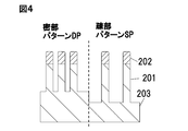
- FIG. 4 shows a shape after etching is performed using the technique of Patent Document 1.
- the second step disclosed in Patent Document 1 is a process using Ar gas and CF 4 gas, and is performed for the purpose of removing a silicon-based reaction product.
- fluorine is involved in the etching of the silicon side wall 201 of Fin, which causes roughness (irregularities) as shown in FIG.
- Patent Document 2 discloses a process of removing a deposited film deposited inside the groove by plasma using a mixed gas of nitrogen trifluoride gas and oxygen gas. However, it is not preferable to additionally execute such a step because the processing time becomes long.
- An object of the present invention is to provide a plasma processing method capable of reducing sparse / dense microloading while reducing the roughness of a silicon sidewall in etching a silicon substrate.
- a typical plasma processing method of the present invention is a plasma processing method of forming STI on a silicon substrate, A trench forming step of forming a trench in the silicon substrate using plasma generated by pulse-modulated high frequency power; After the trench forming step, an oxidizing step of oxidizing the silicon substrate using only oxygen gas, This is achieved by repeating the trench forming step and the oxidizing step a plurality of times.
- FIG. 1 is a schematic diagram of a plasma etching apparatus according to this embodiment.
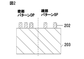
- FIG. 2 is a cross-sectional view of a main portion of a semiconductor substrate for explaining the semiconductor manufacturing process in this embodiment.
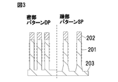
- FIG. 3 is a cross-sectional view of the principal part of the same portion as FIG. 2 during the semiconductor manufacturing process in this embodiment.
- FIG. 4 is a cross-sectional view of an essential part of the same portion as FIG. 2 during a semiconductor manufacturing process in the conventional technique.
- FIG. 5 is a cross-sectional view of the principal part of the same portion as FIG. 2 during the semiconductor manufacturing process in this embodiment.
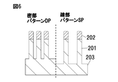
- FIG. 6 is a cross-sectional view of the principal part of the same portion as FIG. 2 during the semiconductor manufacturing process in this embodiment.
- FIG. 7 is a cross-sectional view of the principal part of the same portion as FIG. 2 during the semiconductor manufacturing process in this embodiment.
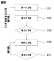
- FIG. 8 is a flowchart of the semiconductor manufacturing process in this embodiment.
- FIG. 1 is a cross-sectional view showing a schematic overall configuration of a plasma processing apparatus used for carrying out the plasma processing method according to the present embodiment.
- the plasma processing apparatus includes a vacuum processing chamber 101, a lower electrode (sample table) 103 provided in the vacuum processing chamber 101, a microwave transmission window 104 such as quartz, and a waveguide 105 provided above the microwave transmission window 104.
- a power control unit 114 for controlling the power supplied to the magnetron drive power supply 113 and the substrate bias power supply 109.
- the lower electrode 103 has a wafer mounting surface that holds the silicon substrate 203.
- the magnetron drive power supply 113 supplies plasma generation power to the magnetron 106, and the substrate bias power supply 109 supplies substrate bias power to the lower electrode 103.
- a wafer carry-in port 110 is provided for loading or unloading the silicon substrate 203 into the vacuum processing chamber 101, and a gas supply port 111 for supplying gas to the vacuum processing chamber 101 is provided.
- an etching gas is supplied from the gas supply port 111 into the vacuum processing chamber 101 to adjust the pressure to a desired value.
- a direct current voltage of several hundred V is applied by the electrostatic attraction power supply 108 to electrostatically attract the silicon substrate 203 to the arrangement surface above the lower electrode 103.
- the magnetron 106 oscillates a microwave having a frequency of 2.45 GHz. This microwave is propagated through the waveguide 105 into the vacuum processing chamber 101.
- the magnetron 106 stops the microwave oscillation.
- a magnetic field is generated in the vacuum processing chamber 101 by the solenoid coil 107, and a high-density plasma 112 is generated in the vacuum processing chamber 101 due to the interaction between the magnetic field and the oscillated microwave.
- high frequency power is supplied from the substrate bias power supply 109 to the lower electrode 103, and the energy of the ions in the plasma incident on the wafer is controlled, so that the silicon substrate 203 can be etched. ..
- Pulsed plasma can be generated by pulse-modulating the electric power supplied to the magnetron 106. More specifically, when the power for plasma generation is turned on / off at a duty ratio of more than 0% and less than 100%, the electron density, electron temperature, and radical density at plasma generation are higher than those at steady discharge. Become. The plasma generated at this time is called pulse plasma.
- the output of the substrate bias power supply 109 is also pulse-modulated, and pulse-modulated power can be applied to the lower electrode 103.
- the power for plasma generation or the substrate bias power is controlled by the power controller 114.
- the duty ratio refers to the ratio of the on time to the total power on / off time.
- the duty ratio of the power for plasma generation can be appropriately changed within the range of 15 to 40%
- the duty ratio of the substrate bias power can be appropriately changed within the range of 5 to 40% according to the specification conditions.
- the substrate bias power is controlled to be turned on only when the plasma generation power is on.
- a hard mask 202 is formed on a silicon substrate 203.
- the hard mask 202 has a dense part pattern DP that is patterned at a predetermined interval and a sparse part pattern SP that is patterned at an interval wider than the dense part pattern DP.
- the interval between the adjacent hard masks 202 in the dense portion pattern DP is 20 nm or less, for example, about 10 nm.
- FIG. 3 shows the shape of the silicon substrate 203 on which fins are formed by the plasma treatment.
- the process of forming the Fin is as follows. (1) Silicon is supplied under a process condition that Cl 2 gas is supplied into the vacuum processing chamber 101 to have a pressure of 0.4 Pa or less and a duty ratio of plasma generation power for forming pulse plasma is 40% or less. The substrate 203 is etched (first step, step S11 in FIG. 8). (2) A mixed gas of SF 6 and CHF 3 is supplied into the vacuum processing chamber 101 to vertically process the silicon substrate 203 (second step, step S12 in FIG. 8).
- the vertical processing refers to processing that is performed substantially perpendicular to the surface of the silicon substrate 203.
- O 2 gas is supplied into the vacuum processing chamber 101, and the surface of the silicon substrate 203 is oxidized under the process conditions of a substrate bias power supply power of 5 W or less and a processing time of 10 seconds or less (third step, FIG. 8 step S13).
- the first step to the third step are repeated a plurality of times to perform etching treatment until the trench depth reaches 40 nm or more.
- the step of repeating the first step to the third step a plurality of times is referred to as a fin forming step of forming fin of fin FET.
- the etching process is performed by repeating the first to third steps seven times, thereby setting the trench depth to 65 nm. Fins are formed between the trenches formed in parallel.
- the etching process is performed until the trench depth becomes 65 nm, but the present invention is not limited to this, and it is sufficient to perform the etching process to a predetermined depth at which Fin can be formed.
- the difference in trench depth due to sparse and dense microloading was 25 nm, but no roughness was generated on the silicon sidewall 201.
- a plasma etching process for reducing sparse and dense microloading is performed.
- a fourth step (trench forming step) using pulsed plasma and Cl 2 gas and a fifth step using only plasma and O 2 gas by continuous discharge.
- the step (oxidation step) is repeated.
- the etching process can be performed without generating roughness on the silicon side wall 201 forming the fin.
- Table 1 collectively shows an example of the processing conditions for the fourth step and the fifth step in the present embodiment.
- a trench is formed in the silicon substrate 203 by etching using the hard mask 202 in the fourth step (step S14 in FIG. 8).
- Cl 2 gas is used as the processing condition
- the flow rate of Cl 2 gas is 200 ml / min or less
- the pressure is 0.3 Pa or less.
- the Cl 2 gas flow rate was 100 ml / min
- the Ar gas flow rate was 30 ml / min
- the CH 4 gas was 4 ml / min or less
- the pressure was 0.1 Pa.
- the fourth step is preferably performed while supplying pulse-modulated high frequency power to the lower electrode 103 on which the silicon substrate 203 is mounted.
- the duty ratio of the pulse-modulated high frequency power for generating plasma is preferably larger than the duty ratio of the pulse modulated high frequency power supplied to the lower electrode 103.
- Ar gas is used in the present embodiment, it may be replaced with He gas or appropriately mixed, and the same effect as in the case of Ar gas alone can be obtained.
- the plasma generation power is 800 W
- the duty ratio is 40%
- the substrate bias power is 400 W
- the duty ratio is 25%
- the plasma generation power and the substrate bias power are pulse-modulated by DualTM (Time Modulation) for synchronization.
- the deposition of the deposit on the hard mask 202 can be suppressed by pulse-modulating with the Dual TM. Further, by lowering the gas pressure, reaction products during etching are reduced, and deposits attached to the hard mask 202 are further reduced.
- the step of removing the silicon-based reaction product as in the second step of the conventional technique is unnecessary, and the roughness of Fin can be reduced. Further, if the processing time of the fourth step is too long, the etching of the sparse part pattern SP is likely to proceed, which causes deterioration of sparse and dense microloading. Therefore, the processing time of the fourth step is set to 8 seconds.
- an oxidized portion 204 is formed on the side surface and the upper surface of the hard mask 202 and the silicon surface.
- the processing conditions of the fifth step plasma was generated with a continuous wave of plasma generation power of 900 W using only O 2 gas, and plasma processing was performed while applying a continuous wave of substrate bias power of 5 W.
- the substrate bias power By applying the substrate bias power, the silicon side wall 201 of the dense portion pattern DP is easily oxidized and the occurrence of roughness is prevented.
- the substrate bias power was set to a continuous wave of 5W.
- the fifth step is preferably performed while supplying unmodulated high frequency power to the lower electrode 103.
- the flow rate of O 2 gas is high, and if the processing time is long, the exposed silicon surface in the region of the dense portion pattern DP is excessively oxidized, so that the fourth step is repeated thereafter. At times, etching of the silicon substrate 203 is hindered. Further, if the pressure is too low, the silicon surface exposed to the sparse part pattern SP is hard to oxidize, so that etching in the depth direction cannot be suppressed, which causes deterioration of sparse / dense microloading. Therefore, the gas flow rate of O 2 is 100 ml / min or less, the pressure is 0.8 Pa or less, and the processing time is 7 seconds.
- the processing time of the fourth step is set to 8 seconds and the processing time of the fifth step is set to 7 seconds.
- the processing time of the fourth step and the fifth step is preferably 10 seconds or less, and thereby the same effect can be obtained.
- the two steps described with reference to FIG. 5 (fourth step) and FIG. 6 (fifth step) are repeatedly etched to a predetermined depth.
- the process is repeated 5 times so that the trench depth becomes 110 nm.
- etching is performed until the trench depth reaches 110 nm, but it is preferable to repeat the fourth step and the fifth step five times or more, whereby etching can be performed so that the trench depth becomes 110 nm or more. it can.
- the reaction product is reduced during the etching in the fourth step, and the excessive deposition of the deposit is avoided by avoiding the excessive protection of the silicon surface in the fifth step. While suppressing, it is possible to realize both the reduction of the sparse and dense microloading and the reduction of the roughness on the silicon sidewall of the Fin.
- the present invention is not limited to the above-described embodiment, and various modifications are included.
- the above-described embodiments have been described in detail in order to explain the present invention in an easy-to-understand manner, and are not necessarily limited to those having all the configurations described.
- a part of the configuration of one embodiment can be replaced with the configuration of another embodiment, and the configuration of another embodiment can be added to the configuration of one embodiment. ..
Landscapes
- Physics & Mathematics (AREA)
- Engineering & Computer Science (AREA)
- Plasma & Fusion (AREA)
- Chemical & Material Sciences (AREA)
- Analytical Chemistry (AREA)
- Drying Of Semiconductors (AREA)
- Element Separation (AREA)
- Crystals, And After-Treatments Of Crystals (AREA)
Abstract
Description
パルス変調された高周波電力により生成されたプラズマを用いて前記シリコン基板にトレンチを形成するトレンチ形成工程と、
前記トレンチ形成工程後、酸素ガスのみを用いて前記シリコン基板を酸化させる酸化工程とを有し、
前記トレンチ形成工程と前記酸化工程を複数回、繰り返すことにより達成される。
上記した以外の課題、構成及び効果は、以下の実施形態の説明により明らかにされる。
(1)真空処理室101内にCl2ガスを供給して0.4Pa以下の圧力とし、且つパルスプラズマを形成するためのプラズマ発生用電力のデューティー比を40%以下とするプロセス条件で、シリコン基板203をエッチングする(第一の工程、図8のステップS11)。
(2)真空処理室101内にSF6とCHF3の混合ガスを供給し、シリコン基板203を垂直加工処理する(第二の工程、図8のステップS12)。ここで、垂直加工処理とは、シリコン基板203の表面に対して略垂直に加工する処理をいう。
(3)真空処理室101内にO2ガスを供給し、基板バイアス電源の電力5W以下、処理時間10秒以下とするプロセス条件で、シリコン基板203の表面を酸化させる(第三の工程、図8のステップS13)。
(4)第一工程から第三の工程を複数回繰り返し、トレンチ深さが40nm以上になるまでエッチング処理を行う。第一工程から第三の工程を複数回繰り返す工程を、fin FETのfinを形成するfin形成工程という。

第四の工程は、パルス変調された高周波電力をシリコン基板203が載置される下部電極103に供給しながら行われると好ましい。また、プラズマを生成するためのパルス変調された高周波電力のデューティー比は、下部電極103に供給されパルス変調された高周波電力のデューティー比より大きいと好ましい。
第五の工程は、変調されていない高周波電力を下部電極103に供給しながら行われると好ましい。
Claims (11)
- シリコン基板にSTIを形成するプラズマ処理方法において、
パルス変調された高周波電力により生成されたプラズマを用いて前記シリコン基板にトレンチを形成するトレンチ形成工程と、
前記トレンチ形成工程後、酸素ガスのみを用いて前記シリコン基板を酸化させる酸化工程とを有し、
前記トレンチ形成工程と前記酸化工程を複数回、繰り返すことを特徴とするプラズマ処理方法。 - 請求項1に記載のプラズマ処理方法において、
前記酸化工程は、連続放電によるプラズマを用いて行われることを特徴とするプラズマ処理方法。 - 請求項1に記載のプラズマ処理方法において、
前記トレンチ形成工程は、パルス変調された高周波電力を前記シリコン基板が載置される試料台に供給しながら行われることを特徴とするプラズマ処理方法。 - 請求項2に記載のプラズマ処理方法において、
前記トレンチ形成工程は、パルス変調された高周波電力を前記シリコン基板が載置される試料台に供給しながら行われることを特徴とするプラズマ処理方法。 - 請求項4に記載のプラズマ処理方法において、
前記プラズマを生成するためのパルス変調された高周波電力のデューティー比は、前記試料台に供給されパルス変調された高周波電力のデューティー比より大きいことを特徴とするプラズマ処理方法。 - 請求項5に記載のプラズマ処理方法において、
前記トレンチ形成工程は、塩素ガスとメタンガスとアルゴンガスの混合ガスを用いて行われることを特徴とするプラズマ処理方法。 - 請求項1に記載のプラズマ処理方法において、
fin FETのfinを形成するfin形成工程をさらに有し、
前記トレンチ形成工程は、前記fin形成工程後に行われることを特徴とするプラズマ処理方法。 - 請求項2に記載のプラズマ処理方法において、
fin FETのfinを形成するfin形成工程をさらに有し、
前記トレンチ形成工程は、前記fin形成工程後に行われることを特徴とするプラズマ処理方法。 - 請求項5に記載のプラズマ処理方法において、
fin FETのfinを形成するfin形成工程をさらに有し、
前記トレンチ形成工程は、前記fin形成工程後に行われることを特徴とするプラズマ処理方法。 - 請求項6に記載のプラズマ処理方法において、
fin FETのfinを形成するfin形成工程をさらに有し、
前記トレンチ形成工程は、前記fin形成工程後に行われることを特徴とするプラズマ処理方法。 - 請求項10に記載のプラズマ処理方法において、
前記酸化工程は、変調されていない高周波電力を前記試料台に供給しながら行われることを特徴とするプラズマ処理方法。
Priority Applications (6)
| Application Number | Priority Date | Filing Date | Title |
|---|---|---|---|
| US16/957,835 US11373875B2 (en) | 2019-06-21 | 2019-06-21 | Plasma processing method |
| KR1020207009881A KR102447235B1 (ko) | 2019-06-21 | 2019-06-21 | 플라스마 처리 방법 |
| PCT/JP2019/024708 WO2020100338A1 (ja) | 2019-06-21 | 2019-06-21 | プラズマ処理方法 |
| JP2020520673A JP7000568B2 (ja) | 2019-06-21 | 2019-06-21 | プラズマ処理方法 |
| CN201980005146.6A CN112424912B (zh) | 2019-06-21 | 2019-06-21 | 等离子处理方法 |
| TW109114150A TWI759732B (zh) | 2019-06-21 | 2020-04-28 | 電漿處理方法 |
Applications Claiming Priority (1)
| Application Number | Priority Date | Filing Date | Title |
|---|---|---|---|
| PCT/JP2019/024708 WO2020100338A1 (ja) | 2019-06-21 | 2019-06-21 | プラズマ処理方法 |
Publications (1)
| Publication Number | Publication Date |
|---|---|
| WO2020100338A1 true WO2020100338A1 (ja) | 2020-05-22 |
Family
ID=70730246
Family Applications (1)
| Application Number | Title | Priority Date | Filing Date |
|---|---|---|---|
| PCT/JP2019/024708 Ceased WO2020100338A1 (ja) | 2019-06-21 | 2019-06-21 | プラズマ処理方法 |
Country Status (6)
| Country | Link |
|---|---|
| US (1) | US11373875B2 (ja) |
| JP (1) | JP7000568B2 (ja) |
| KR (1) | KR102447235B1 (ja) |
| CN (1) | CN112424912B (ja) |
| TW (1) | TWI759732B (ja) |
| WO (1) | WO2020100338A1 (ja) |
Cited By (1)
| Publication number | Priority date | Publication date | Assignee | Title |
|---|---|---|---|---|
| WO2024023877A1 (ja) * | 2022-07-25 | 2024-02-01 | 株式会社日立ハイテク | プラズマ処理方法 |
Families Citing this family (2)
| Publication number | Priority date | Publication date | Assignee | Title |
|---|---|---|---|---|
| US20200135898A1 (en) * | 2018-10-30 | 2020-04-30 | International Business Machines Corporation | Hard mask replenishment for etching processes |
| US12557575B2 (en) * | 2022-12-22 | 2026-02-17 | Taiwan Semiconductor Manufacturing Company, Ltd. | Methods for reducing leakage current |
Citations (5)
| Publication number | Priority date | Publication date | Assignee | Title |
|---|---|---|---|---|
| JP2001110783A (ja) * | 1999-10-12 | 2001-04-20 | Hitachi Ltd | プラズマ処理装置およびプラズマ処理方法 |
| JP2010287823A (ja) * | 2009-06-15 | 2010-12-24 | Denso Corp | 半導体装置の製造方法 |
| JP2013030776A (ja) * | 2011-07-27 | 2013-02-07 | Advanced Ion Beam Technology Inc | 代用ソース/ドレインフィンfet加工 |
| JP2014204050A (ja) * | 2013-04-09 | 2014-10-27 | 株式会社日立ハイテクノロジーズ | プラズマ処理方法およびプラズマ処理装置 |
| JP2015050440A (ja) * | 2013-09-04 | 2015-03-16 | 株式会社日立ハイテクノロジーズ | プラズマ処理方法 |
Family Cites Families (12)
| Publication number | Priority date | Publication date | Assignee | Title |
|---|---|---|---|---|
| CN101153396B (zh) * | 2006-09-30 | 2010-06-09 | 中芯国际集成电路制造(上海)有限公司 | 等离子刻蚀方法 |
| JP5229711B2 (ja) * | 2006-12-25 | 2013-07-03 | 国立大学法人名古屋大学 | パターン形成方法、および半導体装置の製造方法 |
| US20110061812A1 (en) * | 2009-09-11 | 2011-03-17 | Applied Materials, Inc. | Apparatus and Methods for Cyclical Oxidation and Etching |
| JP2011211135A (ja) * | 2010-03-31 | 2011-10-20 | Hitachi High-Technologies Corp | プラズマ処理方法 |
| US9324576B2 (en) * | 2010-05-27 | 2016-04-26 | Applied Materials, Inc. | Selective etch for silicon films |
| JP2014220360A (ja) | 2013-05-08 | 2014-11-20 | 株式会社日立ハイテクノロジーズ | プラズマ処理方法 |
| CN104425339B (zh) * | 2013-08-20 | 2017-09-22 | 中芯国际集成电路制造(上海)有限公司 | 用于鳍式场效应晶体管的浅沟槽隔离结构的形成方法 |
| US10204794B2 (en) | 2013-12-23 | 2019-02-12 | Intel Corporation | Advanced etching technologies for straight, tall and uniform fins across multiple fin pitch structures |
| CN103871902A (zh) * | 2014-03-24 | 2014-06-18 | 上海华力微电子有限公司 | 半导体处理工艺及半导体器件的制备方法 |
| US9240315B1 (en) * | 2014-10-10 | 2016-01-19 | Applied Materials, Inc. | CVD oxide surface pre-conditioning by inductively coupled O2 plasma |
| US9966312B2 (en) * | 2015-08-25 | 2018-05-08 | Tokyo Electron Limited | Method for etching a silicon-containing substrate |
| US10037890B2 (en) * | 2016-10-11 | 2018-07-31 | Lam Research Corporation | Method for selectively etching with reduced aspect ratio dependence |
-
2019
- 2019-06-21 WO PCT/JP2019/024708 patent/WO2020100338A1/ja not_active Ceased
- 2019-06-21 JP JP2020520673A patent/JP7000568B2/ja active Active
- 2019-06-21 KR KR1020207009881A patent/KR102447235B1/ko active Active
- 2019-06-21 CN CN201980005146.6A patent/CN112424912B/zh active Active
- 2019-06-21 US US16/957,835 patent/US11373875B2/en active Active
-
2020
- 2020-04-28 TW TW109114150A patent/TWI759732B/zh active
Patent Citations (5)
| Publication number | Priority date | Publication date | Assignee | Title |
|---|---|---|---|---|
| JP2001110783A (ja) * | 1999-10-12 | 2001-04-20 | Hitachi Ltd | プラズマ処理装置およびプラズマ処理方法 |
| JP2010287823A (ja) * | 2009-06-15 | 2010-12-24 | Denso Corp | 半導体装置の製造方法 |
| JP2013030776A (ja) * | 2011-07-27 | 2013-02-07 | Advanced Ion Beam Technology Inc | 代用ソース/ドレインフィンfet加工 |
| JP2014204050A (ja) * | 2013-04-09 | 2014-10-27 | 株式会社日立ハイテクノロジーズ | プラズマ処理方法およびプラズマ処理装置 |
| JP2015050440A (ja) * | 2013-09-04 | 2015-03-16 | 株式会社日立ハイテクノロジーズ | プラズマ処理方法 |
Cited By (3)
| Publication number | Priority date | Publication date | Assignee | Title |
|---|---|---|---|---|
| WO2024023877A1 (ja) * | 2022-07-25 | 2024-02-01 | 株式会社日立ハイテク | プラズマ処理方法 |
| JPWO2024023877A1 (ja) * | 2022-07-25 | 2024-02-01 | ||
| JP7519549B2 (ja) | 2022-07-25 | 2024-07-19 | 株式会社日立ハイテク | プラズマ処理方法 |
Also Published As
| Publication number | Publication date |
|---|---|
| TW202101585A (zh) | 2021-01-01 |
| CN112424912A (zh) | 2021-02-26 |
| KR102447235B1 (ko) | 2022-09-27 |
| US11373875B2 (en) | 2022-06-28 |
| TWI759732B (zh) | 2022-04-01 |
| KR20200145823A (ko) | 2020-12-30 |
| CN112424912B (zh) | 2024-01-05 |
| US20210066087A1 (en) | 2021-03-04 |
| JP7000568B2 (ja) | 2022-01-19 |
| JPWO2020100338A1 (ja) | 2021-02-15 |
Similar Documents
| Publication | Publication Date | Title |
|---|---|---|
| JP6138653B2 (ja) | ドライエッチング方法 | |
| JP6719602B2 (ja) | 材料改質とrfパルスを用いた選択的エッチング | |
| KR102460164B1 (ko) | 에칭 방법 | |
| US11205577B2 (en) | Method of selectively etching silicon oxide film on substrate | |
| KR102513051B1 (ko) | 에칭 방법 | |
| US12230505B2 (en) | Etching apparatus | |
| JP5214596B2 (ja) | プラズマ処理システムのマスクアンダーカットおよびノッチを最小化する方法 | |
| CN102403183A (zh) | 等离子体蚀刻处理装置及其方法和半导体元件制造方法 | |
| TWI759732B (zh) | 電漿處理方法 | |
| JP7054759B2 (ja) | プラズマ処理方法 | |
| JP6579786B2 (ja) | プラズマエッチング方法 | |
| JP2014220360A (ja) | プラズマ処理方法 | |
| JP5774356B2 (ja) | プラズマ処理方法 | |
| JP6113608B2 (ja) | プラズマエッチング方法 | |
| KR102916926B1 (ko) | 플라스마 처리 방법 | |
| JP5918886B2 (ja) | プラズマ処理方法 |
Legal Events
| Date | Code | Title | Description |
|---|---|---|---|
| ENP | Entry into the national phase |
Ref document number: 20207009881 Country of ref document: KR Kind code of ref document: A |
|
| ENP | Entry into the national phase |
Ref document number: 2020520673 Country of ref document: JP Kind code of ref document: A |
|
| 121 | Ep: the epo has been informed by wipo that ep was designated in this application |
Ref document number: 19885057 Country of ref document: EP Kind code of ref document: A1 |
|
| NENP | Non-entry into the national phase |
Ref country code: DE |
|
| 122 | Ep: pct application non-entry in european phase |
Ref document number: 19885057 Country of ref document: EP Kind code of ref document: A1 |