WO2020095540A1 - 撮像装置及び電子機器 - Google Patents
撮像装置及び電子機器 Download PDFInfo
- Publication number
- WO2020095540A1 WO2020095540A1 PCT/JP2019/036091 JP2019036091W WO2020095540A1 WO 2020095540 A1 WO2020095540 A1 WO 2020095540A1 JP 2019036091 W JP2019036091 W JP 2019036091W WO 2020095540 A1 WO2020095540 A1 WO 2020095540A1
- Authority
- WO
- WIPO (PCT)
- Prior art keywords
- pixel
- wiring
- switch element
- voltage
- defect
- Prior art date
- Legal status (The legal status is an assumption and is not a legal conclusion. Google has not performed a legal analysis and makes no representation as to the accuracy of the status listed.)
- Ceased
Links
Images






Classifications
-
- H—ELECTRICITY
- H10—SEMICONDUCTOR DEVICES; ELECTRIC SOLID-STATE DEVICES NOT OTHERWISE PROVIDED FOR
- H10F—INORGANIC SEMICONDUCTOR DEVICES SENSITIVE TO INFRARED RADIATION, LIGHT, ELECTROMAGNETIC RADIATION OF SHORTER WAVELENGTH OR CORPUSCULAR RADIATION
- H10F39/00—Integrated devices, or assemblies of multiple devices, comprising at least one element covered by group H10F30/00, e.g. radiation detectors comprising photodiode arrays
- H10F39/10—Integrated devices
- H10F39/12—Image sensors
- H10F39/18—Complementary metal-oxide-semiconductor [CMOS] image sensors; Photodiode array image sensors
-
- G—PHYSICS
- G01—MEASURING; TESTING
- G01R—MEASURING ELECTRIC VARIABLES; MEASURING MAGNETIC VARIABLES
- G01R31/00—Arrangements for testing electric properties; Arrangements for locating electric faults; Arrangements for electrical testing characterised by what is being tested not provided for elsewhere
- G01R31/50—Testing of electric apparatus, lines, cables or components for short-circuits, continuity, leakage current or incorrect line connections
- G01R31/54—Testing for continuity
-
- H—ELECTRICITY
- H04—ELECTRIC COMMUNICATION TECHNIQUE
- H04N—PICTORIAL COMMUNICATION, e.g. TELEVISION
- H04N17/00—Diagnosis, testing or measuring for television systems or their details
- H04N17/002—Diagnosis, testing or measuring for television systems or their details for television cameras
-
- H—ELECTRICITY
- H04—ELECTRIC COMMUNICATION TECHNIQUE
- H04N—PICTORIAL COMMUNICATION, e.g. TELEVISION
- H04N25/00—Circuitry of solid-state image sensors [SSIS]; Control thereof
- H04N25/60—Noise processing, e.g. detecting, correcting, reducing or removing noise
- H04N25/68—Noise processing, e.g. detecting, correcting, reducing or removing noise applied to defects
- H04N25/69—SSIS comprising testing or correcting structures for circuits other than pixel cells
-
- H—ELECTRICITY
- H04—ELECTRIC COMMUNICATION TECHNIQUE
- H04N—PICTORIAL COMMUNICATION, e.g. TELEVISION
- H04N25/00—Circuitry of solid-state image sensors [SSIS]; Control thereof
- H04N25/70—SSIS architectures; Circuits associated therewith
- H04N25/76—Addressed sensors, e.g. MOS or CMOS sensors
- H04N25/78—Readout circuits for addressed sensors, e.g. output amplifiers or A/D converters
-
- H—ELECTRICITY
- H04—ELECTRIC COMMUNICATION TECHNIQUE
- H04N—PICTORIAL COMMUNICATION, e.g. TELEVISION
- H04N25/00—Circuitry of solid-state image sensors [SSIS]; Control thereof
- H04N25/70—SSIS architectures; Circuits associated therewith
- H04N25/79—Arrangements of circuitry being divided between different or multiple substrates, chips or circuit boards, e.g. stacked image sensors
-
- H—ELECTRICITY
- H10—SEMICONDUCTOR DEVICES; ELECTRIC SOLID-STATE DEVICES NOT OTHERWISE PROVIDED FOR
- H10F—INORGANIC SEMICONDUCTOR DEVICES SENSITIVE TO INFRARED RADIATION, LIGHT, ELECTROMAGNETIC RADIATION OF SHORTER WAVELENGTH OR CORPUSCULAR RADIATION
- H10F39/00—Integrated devices, or assemblies of multiple devices, comprising at least one element covered by group H10F30/00, e.g. radiation detectors comprising photodiode arrays
- H10F39/011—Manufacture or treatment of image sensors covered by group H10F39/12
- H10F39/018—Manufacture or treatment of image sensors covered by group H10F39/12 of hybrid image sensors
-
- H—ELECTRICITY
- H10—SEMICONDUCTOR DEVICES; ELECTRIC SOLID-STATE DEVICES NOT OTHERWISE PROVIDED FOR
- H10F—INORGANIC SEMICONDUCTOR DEVICES SENSITIVE TO INFRARED RADIATION, LIGHT, ELECTROMAGNETIC RADIATION OF SHORTER WAVELENGTH OR CORPUSCULAR RADIATION
- H10F39/00—Integrated devices, or assemblies of multiple devices, comprising at least one element covered by group H10F30/00, e.g. radiation detectors comprising photodiode arrays
- H10F39/80—Constructional details of image sensors
- H10F39/802—Geometry or disposition of elements in pixels, e.g. address-lines or gate electrodes
- H10F39/8023—Disposition of the elements in pixels, e.g. smaller elements in the centre of the imager compared to larger elements at the periphery
-
- H—ELECTRICITY
- H10—SEMICONDUCTOR DEVICES; ELECTRIC SOLID-STATE DEVICES NOT OTHERWISE PROVIDED FOR
- H10F—INORGANIC SEMICONDUCTOR DEVICES SENSITIVE TO INFRARED RADIATION, LIGHT, ELECTROMAGNETIC RADIATION OF SHORTER WAVELENGTH OR CORPUSCULAR RADIATION
- H10F39/00—Integrated devices, or assemblies of multiple devices, comprising at least one element covered by group H10F30/00, e.g. radiation detectors comprising photodiode arrays
- H10F39/80—Constructional details of image sensors
- H10F39/803—Pixels having integrated switching, control, storage or amplification elements
- H10F39/8033—Photosensitive area
-
- H—ELECTRICITY
- H10—SEMICONDUCTOR DEVICES; ELECTRIC SOLID-STATE DEVICES NOT OTHERWISE PROVIDED FOR
- H10F—INORGANIC SEMICONDUCTOR DEVICES SENSITIVE TO INFRARED RADIATION, LIGHT, ELECTROMAGNETIC RADIATION OF SHORTER WAVELENGTH OR CORPUSCULAR RADIATION
- H10F39/00—Integrated devices, or assemblies of multiple devices, comprising at least one element covered by group H10F30/00, e.g. radiation detectors comprising photodiode arrays
- H10F39/80—Constructional details of image sensors
- H10F39/803—Pixels having integrated switching, control, storage or amplification elements
- H10F39/8037—Pixels having integrated switching, control, storage or amplification elements the integrated elements comprising a transistor
-
- H—ELECTRICITY
- H10—SEMICONDUCTOR DEVICES; ELECTRIC SOLID-STATE DEVICES NOT OTHERWISE PROVIDED FOR
- H10F—INORGANIC SEMICONDUCTOR DEVICES SENSITIVE TO INFRARED RADIATION, LIGHT, ELECTROMAGNETIC RADIATION OF SHORTER WAVELENGTH OR CORPUSCULAR RADIATION
- H10F39/00—Integrated devices, or assemblies of multiple devices, comprising at least one element covered by group H10F30/00, e.g. radiation detectors comprising photodiode arrays
- H10F39/80—Constructional details of image sensors
- H10F39/807—Pixel isolation structures
-
- H—ELECTRICITY
- H10—SEMICONDUCTOR DEVICES; ELECTRIC SOLID-STATE DEVICES NOT OTHERWISE PROVIDED FOR
- H10F—INORGANIC SEMICONDUCTOR DEVICES SENSITIVE TO INFRARED RADIATION, LIGHT, ELECTROMAGNETIC RADIATION OF SHORTER WAVELENGTH OR CORPUSCULAR RADIATION
- H10F39/00—Integrated devices, or assemblies of multiple devices, comprising at least one element covered by group H10F30/00, e.g. radiation detectors comprising photodiode arrays
- H10F39/80—Constructional details of image sensors
- H10F39/809—Constructional details of image sensors of hybrid image sensors
-
- H—ELECTRICITY
- H10—SEMICONDUCTOR DEVICES; ELECTRIC SOLID-STATE DEVICES NOT OTHERWISE PROVIDED FOR
- H10F—INORGANIC SEMICONDUCTOR DEVICES SENSITIVE TO INFRARED RADIATION, LIGHT, ELECTROMAGNETIC RADIATION OF SHORTER WAVELENGTH OR CORPUSCULAR RADIATION
- H10F39/00—Integrated devices, or assemblies of multiple devices, comprising at least one element covered by group H10F30/00, e.g. radiation detectors comprising photodiode arrays
- H10F39/80—Constructional details of image sensors
- H10F39/811—Interconnections
-
- H—ELECTRICITY
- H10—SEMICONDUCTOR DEVICES; ELECTRIC SOLID-STATE DEVICES NOT OTHERWISE PROVIDED FOR
- H10P—GENERIC PROCESSES OR APPARATUS FOR THE MANUFACTURE OR TREATMENT OF DEVICES COVERED BY CLASS H10
- H10P14/00—Formation of materials, e.g. in the shape of layers or pillars
- H10P14/40—Formation of materials, e.g. in the shape of layers or pillars of conductive or resistive materials
-
- H—ELECTRICITY
- H10—SEMICONDUCTOR DEVICES; ELECTRIC SOLID-STATE DEVICES NOT OTHERWISE PROVIDED FOR
- H10W—GENERIC PACKAGES, INTERCONNECTIONS, CONNECTORS OR OTHER CONSTRUCTIONAL DETAILS OF DEVICES COVERED BY CLASS H10
- H10W20/00—Interconnections in chips, wafers or substrates
- H10W20/01—Manufacture or treatment
-
- H—ELECTRICITY
- H10—SEMICONDUCTOR DEVICES; ELECTRIC SOLID-STATE DEVICES NOT OTHERWISE PROVIDED FOR
- H10W—GENERIC PACKAGES, INTERCONNECTIONS, CONNECTORS OR OTHER CONSTRUCTIONAL DETAILS OF DEVICES COVERED BY CLASS H10
- H10W20/00—Interconnections in chips, wafers or substrates
- H10W20/40—Interconnections external to wafers or substrates, e.g. back-end-of-line [BEOL] metallisations or vias connecting to gate electrodes
Definitions
- the present disclosure relates to an imaging device and an electronic device.
- a plurality of light-receiving elements is divided into several element groups, and an inspection pad is provided corresponding to each element group. Then, each element group is connected to a common inspection signal line, both the output circuit and the input circuit are connected to each inspection pad, and the changeover switch connects the inspection signal line to the corresponding inspection pad. By connecting to either the output circuit or the input circuit of, the inspection pad can be used to inspect the light receiving element.
- the light-receiving chip described in Patent Document 1 described above is intended for the inspection of the light-receiving element in the state before the perforated electrode for outputting the light-receiving signal is formed.
- An object of the present disclosure is to provide an imaging device that can inspect a wiring formed for each pixel row or each pixel column with a minimum of additional circuits and an electronic device including the imaging device.
- An imaging device of the present disclosure for achieving the above object is A first substrate on which a pixel array unit formed by arranging pixels including light receiving units in a matrix is formed; and a second substrate on which a pixel control unit for controlling pixels is formed,
- the first substrate is A first wiring transmitting a first voltage, A second wire for transmitting a second voltage, and
- a defect detection circuit for detecting a wiring defect is provided for each pixel block, The defect detection circuit
- a wiring defect is detected, a plurality of wirings corresponding to a plurality of pixel columns or a plurality of pixel rows are connected in series for each pixel block, and one end of a wiring chain connected in series in each pixel block is connected to the first wiring. And the other end to the second wire, Wiring failure is detected based on the potential at the intermediate position of the wiring chain.
- the electronic device of the present disclosure for achieving the above object includes the image pickup apparatus having the above configuration.
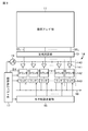
- FIG. 1 is a block diagram showing an outline of a basic configuration of a CMOS image sensor which is an example of the image pickup apparatus of the present disclosure.
- FIG. 2 is a circuit diagram showing an example of a circuit configuration of a pixel.
- FIG. 3 is a block diagram showing an example of the configuration of a column parallel analog-digital conversion unit mounted on the CMOS image sensor.
- FIG. 4 is an exploded perspective view showing an outline of a laminated chip structure.
- FIG. 5 is a schematic view showing a chip bonding procedure in a COW type laminated structure.
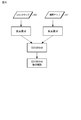
- FIG. 6 is a process diagram showing a flow of a chip bonding process in a COW type laminated structure.
- FIG. 7 is a diagram for explaining a method of detecting an open wiring defect.
- FIG. 1 is a block diagram showing an outline of a basic configuration of a CMOS image sensor which is an example of the image pickup apparatus of the present disclosure.
- FIG. 2 is a circuit diagram showing an example of
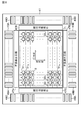
- FIG. 8 is a schematic configuration diagram illustrating an example of a basic configuration of the pixel chip according to the first embodiment.
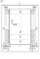
- FIG. 9 is a circuit diagram showing an example of a specific configuration of the pixel chip according to the second embodiment.
- FIG. 10 is a circuit diagram showing an example of a daisy chain in one pixel block of the pixel array section and a circuit configuration of two defect detection circuits.
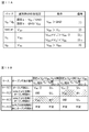
- FIG. 11A illustrates setting of each voltage value of the first voltage V a / second voltage V b / third voltage V c / fourth voltage V d and restriction when the open defect is detected.
- FIG. 11B is a diagram illustrating case classification that occurs when an open defect is detected.
- FIG. 12 is a diagram illustrating a leak current generated when performing the disconnection inspection.
- FIG. 11A illustrates setting of each voltage value of the first voltage V a / second voltage V b / third voltage V c / fourth voltage V d and restriction when the open defect is detected.
- FIG. 11B is
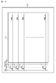
- FIG. 13 is a diagram illustrating an example of a method for preventing erroneous detection of disconnection due to a leak current.
- FIG. 14 is a diagram illustrating an application example of the technology according to the present disclosure.
- FIG. 15 is a block diagram showing an outline of a configuration of an imaging system which is an example of the electronic device of the present disclosure.
- FIG. 16 is a diagram showing an example of a schematic configuration of an endoscopic surgery system to which the technology according to the present disclosure can be applied.
- FIG. 17 is a block diagram showing an example of the functional configuration of the camera head and the CCU in the endoscopic surgery system.
- FIG. 18 is a block diagram showing a schematic configuration example of a vehicle control system which is an example of a mobile body control system to which the technology according to the present disclosure can be applied.
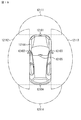
- FIG. 19 is a diagram illustrating an example of the installation position of the imaging unit in the mobile control system.
- Example 2 (Specific configuration example of pixel chip according to Example 1) 4. Modification 5.
- Application example 6 Application example of technology according to the present disclosure 6-1.
- Electronic device of the present disclosure (example of imaging system) 6-2.
- Application example to endoscopic surgery system 6-3.
- the defect detection circuit when detecting a wiring defect, a plurality of lines are connected in series between the first line and the second line for each pixel block.
- a configuration having a switch element group that constitutes a wiring chain can be obtained.
- the switch element at one end of the switch element group may be connected to the first wiring and the switch element at the other end may be connected to the second wiring.
- the third wiring for transmitting the third voltage and the fourth wiring for transmitting the fourth voltage are provided on the first substrate. Can be provided. Further, regarding the defect detection circuit, a first switch element connected to an intermediate position of the wiring chain and reading the potential at the intermediate position, and connected between the third wiring and the fourth wiring, the first switch A configuration having a second switch element that performs on / off operation according to the potential at the intermediate position read through the element can be adopted.
- the failure detection circuit in the failure detection circuit, wiring failure occurs depending on whether or not a short current is generated between the third wiring and the fourth wiring. Can be detected.
- the failure detection circuit may be configured to detect a wire disconnection failure between one end and an intermediate position of the wiring chain or a wire disconnection failure between the intermediate position and the other end of the wiring chain. it can.
- each switch element of the switch element group of the defect detection circuit, the first switch element, and the second switch element have a pixel. It is possible to adopt a structure including a transistor of the same conductivity type as the constituent transistor. Specifically, when the transistor forming the pixel is an N-channel MOS transistor, each switch element of the switch element group of the defect detection circuit, the first switch element, and the second switch element are of the same type as the pixel.
- the N channel MOS transistor can be used.
- CMOS Complementary Metal Oxide Semiconductor
- CMOS image sensor which is a type of an XY addressing type imaging device, will be described as an example of the imaging device.
- the CMOS image sensor is an image sensor manufactured by applying a CMOS process or partially using it.
- FIG. 1 is a block diagram showing an outline of a basic configuration of a CMOS image sensor which is an example of the image pickup apparatus of the present disclosure.
- the CMOS image sensor 1 has a configuration including a pixel array section 11 and a peripheral circuit section of the pixel array section 11.
- the pixel array unit 11 includes pixels 2 including light receiving units (photoelectric conversion units) arranged two-dimensionally in the row direction and the column direction, that is, in a matrix.
- the row direction means the arrangement direction of the pixels 2 in the pixel row (so-called horizontal direction)
- the column direction means the arrangement direction of the pixels 2 in the pixel column (so-called vertical direction).
- the pixel 2 performs photoelectric conversion to generate and accumulate photocharges according to the amount of received light.
- the peripheral circuit section of the pixel array section 11 includes, for example, a row selection section 12, a constant current source section 13, an analog-digital conversion section 14, a horizontal transfer scanning section 15, a signal processing section 16, a timing control section 17, and the like. Has been done.
- pixel control lines 31 1 to 31 m are arranged along the row direction for each pixel row with respect to the matrix-shaped pixel array. Is wired.
- vertical signal lines 32 1 to 32 n (hereinafter, may be collectively referred to as “vertical signal line 32”) are arranged along the column direction for each pixel column.
- the pixel control line 31 transmits a drive signal for driving when reading a signal from the pixel 2.
- the pixel control line 31 is illustrated as one wiring, but the number is not limited to one.
- One end of the pixel control line 31 is connected to the output end corresponding to each row of the row selection unit 12.
- the control unit 17 will be described.
- the row selection unit 12 is configured by a shift register, an address decoder, and the like, and controls the scanning of the pixel row and the address of the pixel row when selecting each pixel 2 of the pixel array unit 11.
- the row selection section 12 generally has two scanning systems, a read scanning system and a sweep scanning system.
- the read scanning system sequentially selects and scans the pixels 2 of the pixel array unit 11 in units of rows in order to read pixel signals from the pixels 2.
- the pixel signal read from the pixel 2 is an analog signal.
- the sweep-out scanning system performs sweep-out scanning with respect to the read-out row in which read-out scanning is performed by the read-out scanning system, prior to the read-out scanning by the shutter speed time.
- the electronic shutter operation refers to an operation of discarding the photocharges of the photoelectric conversion unit and newly starting the exposure (starting the accumulation of the photocharges).
- the constant current source unit 13 includes a plurality of current sources I each composed of, for example, a MOS transistor, connected to each of the vertical signal lines 32 1 to 32 n for each pixel column, and selectively scanned by the row selection unit 12. A bias current is supplied to each pixel 2 in the pixel row through each of the vertical signal lines 32 1 to 32 n .
- the analog-digital conversion unit 14 is formed of a set of a plurality of analog-digital converters provided corresponding to the pixel columns of the pixel array unit 11, for example, provided for each pixel column.
- the analog-digital conversion unit 14 is a column parallel type analog-digital conversion unit that converts an analog pixel signal output through each of the vertical signal lines 32 1 to 32 n for each pixel column into an N-bit digital signal. is there.
- analog-digital converter in the column parallel analog-digital converter 14 for example, a single slope type analog-digital converter which is an example of a reference signal comparison type analog-digital converter can be used.
- analog-digital converter is not limited to a single slope type analog-digital converter, but a successive approximation type analog-digital converter, a delta-sigma modulation type ( ⁇ modulation type) analog-digital converter, etc. Can be used.
- the horizontal transfer scanning unit 15 is composed of a shift register, an address decoder, and the like, and controls the scanning of the pixel column and the address of the pixel column when reading the signal of each pixel 2 of the pixel array unit 11. Under the control of the horizontal transfer scanning unit 15, the pixel signal converted into a digital signal by the analog-digital conversion unit 14 is read out to the horizontal transfer line 18 having a 2N-bit width in pixel column units.
- the signal processing unit 16 performs predetermined signal processing on the digital pixel signal supplied through the horizontal transfer line 18 to generate two-dimensional image data. For example, the signal processing unit 16 corrects vertical line defects and point defects, or clamps signals, and performs digital signal processing such as parallel-serial conversion, compression, encoding, addition, averaging, and intermittent operation. Or The signal processing unit 16 outputs the generated image data as an output signal of the CMOS image sensor 1 to a device in the subsequent stage.
- the timing control unit 17 generates various timing signals, clock signals, control signals, and the like, and based on these generated signals, the row selection unit 12, the constant current source unit 13, the analog-digital conversion unit 14, the horizontal Drive control of the transfer scanning unit 15, the signal processing unit 16 and the like is performed.
- FIG. 2 is a circuit diagram showing an example of the circuit configuration of the pixel 2.
- the pixel 2 has, for example, a photodiode 21 as a photoelectric conversion unit that is a light receiving unit.
- the pixel 2 has a pixel configuration including a transfer transistor 22, a reset transistor 23, an amplification transistor 24, and a selection transistor 25 in addition to the photodiode 21.
- the four transistors of the transfer transistor 22, the reset transistor 23, the amplification transistor 24, and the selection transistor 25, for example, N-channel MOS type field effect transistors (FETs) are used.
- FETs field effect transistors
- the pixel 2 By configuring the pixel 2 with only N-channel transistors, it is possible to optimize the area efficiency and the process reduction viewpoint.
- the combination of the conductivity types of the four transistors 22 to 25 illustrated here is merely an example, and the present invention is not limited to these combinations.
- a plurality of control lines are wired commonly to each pixel 2 in the same pixel row.
- the plurality of control lines are connected to the output terminals of the row selection unit 12 corresponding to each pixel row in pixel row units.
- the row selection unit 12 appropriately outputs the transfer signal TRG, the reset signal RST, and the selection signal SEL to the plurality of control lines.
- the photodiode 21 has an anode electrode connected to a low-potential-side power source (eg, ground), and photoelectrically converts the received light into a photocharge (here, photoelectron) having a charge amount corresponding to the light amount thereof. Accumulates electric charge.
- the cathode electrode of the photodiode 21 is electrically connected to the gate electrode of the amplification transistor 24 via the transfer transistor 22.
- the region where the gate electrode of the amplification transistor 24 is electrically connected is a floating diffusion (floating diffusion region / impurity diffusion region) FD.
- the floating diffusion FD is a charge-voltage converter that converts charges into a voltage.
- a transfer signal TRG that activates a high level (for example, V DD level) is applied to the gate electrode of the transfer transistor 22 from the row selection unit 12.
- the transfer transistor 22 becomes conductive in response to the transfer signal TRG, and thus photoelectrically converts in the photodiode 21 and transfers the photocharges accumulated in the photodiode 21 to the floating diffusion FD.
- the reset transistor 23 is connected between the node of the high-potential-side power supply voltage V DD and the floating diffusion FD.
- a reset signal RST that activates a high level is applied to the gate electrode of the reset transistor 23 from the row selection unit 12.
- the reset transistor 23 becomes conductive in response to the reset signal RST, and resets the floating diffusion FD by discarding the charge of the floating diffusion FD to the node of the voltage V DD .
- the gate electrode is connected to the floating diffusion FD and the drain electrode is connected to the node of the high potential side power supply voltage V DD .
- the amplification transistor 24 serves as an input unit of a source follower that reads out a signal obtained by photoelectric conversion in the photodiode 21. That is, the source electrode of the amplification transistor 24 is connected to the vertical signal line 32 via the selection transistor 25.
- the amplification transistor 24 and the current source I connected to one end of the vertical signal line 32 constitute a source follower that converts the voltage of the floating diffusion FD into the potential of the vertical signal line 32.
- the drain electrode of the selection transistor 25 is connected to the source electrode of the amplification transistor 24, and the source electrode is connected to the vertical signal line 32.
- a selection signal SEL that activates the high level is applied to the gate electrode of the selection transistor 25 from the row selection unit 12.
- the selection transistor 25 is rendered conductive in response to the selection signal SEL, and thereby transfers the signal output from the amplification transistor 24 to the vertical signal line 32 with the pixel 2 in the selected state.
- the selection transistor 25 may have a circuit configuration connected between the node of the high-potential-side power supply voltage V DD and the drain electrode of the amplification transistor 24. Further, in this example, as the pixel circuit of the pixel 2, the 4Tr configuration including the transfer transistor 22, the reset transistor 23, the amplification transistor 24, and the selection transistor 25, that is, four transistors (Tr) has been described as an example. , But is not limited to this.
- the selection transistor 25 may be omitted, and the amplification transistor 24 may have a 3Tr configuration in which the function of the selection transistor 25 is provided. If necessary, the number of transistors may be increased to 5Tr or more. ..
- FIG. 3 is a block diagram showing an example of the configuration of the column parallel analog-digital conversion unit 14.
- the analog-digital converter 14 in the CMOS image sensor 1 of the present disclosure is composed of a set of a plurality of single slope type analog-digital converters provided corresponding to the vertical signal lines 32 1 to 32 n .
- the single-slope analog-digital converter 140 in the n-th column will be described as an example.
- the single-slope analog-digital converter 140 has a circuit configuration including a comparator 141, a counter circuit 142, and a latch circuit 143.
- the single-slope analog-to-digital converter 140 uses a so-called RAMP waveform (slope waveform) reference signal whose voltage value changes linearly with the passage of time.
- the reference signal having the ramp waveform is generated by the reference signal generation unit 19.
- the reference signal generation unit 19 can be configured using, for example, a DAC (digital-analog conversion) circuit.
- the comparator 141 uses the analog pixel signal read from the pixel 2 as a comparison input and the ramp waveform reference signal generated by the reference signal generation unit 19 as a reference input, and compares the two signals. Then, for example, when the reference signal is larger than the pixel signal, the output of the comparator 141 is in the first state (for example, high level), and when the reference signal is less than or equal to the pixel signal, the output is in the second state ( For example, low level). Accordingly, the comparator 141 outputs a pulse signal having a pulse width corresponding to the signal level of the pixel signal, specifically, the magnitude of the signal level, as a comparison result.
- the clock signal CLK is given to the counter circuit 142 from the timing control unit 17 at the same timing as the timing of starting the supply of the reference signal to the comparator 141. Then, the counter circuit 142 measures the pulse width period of the output pulse of the comparator 141, that is, the period from the start of the comparison operation to the end of the comparison operation by performing the counting operation in synchronization with the clock signal CLK. ..
- the count result (count value) of the counter circuit 142 becomes a digital value obtained by digitizing an analog pixel signal.
- the latch circuit 143 holds (latches) the digital value that is the count result of the counter circuit 142. Further, the latch circuit 143 is an example of noise removal processing by calculating the difference between the D-phase count value corresponding to the signal level pixel signal and the P-phase count value corresponding to the reset level pixel signal. , CDS (Correlated Double Sampling). Then, under the drive of the horizontal transfer scanning unit 15, the latched digital value is output to the horizontal transfer line 18.
- the reference signal of the linearly changing analog value generated by the reference signal generation unit 19 and the pixel A digital value is obtained from time information until the magnitude relationship with the analog pixel signal output from 2 changes.
- the analog-to-digital conversion unit 14 in which the analog-to-digital converter 140 is arranged in a one-to-one relationship with the pixel column is illustrated, but the analog-to-digital conversion is performed in units of a plurality of pixel columns. It is also possible to use the analog-digital conversion unit 14 in which the converter 140 is arranged.
- the chip (semiconductor integrated circuit) structure of the CMOS image sensor 1 having the above configuration has a laminated chip structure (so-called laminated chip).
- laminated chip when the substrate surface on the side where the wiring layer is formed is the front surface (front surface), the back surface irradiation type pixel structure that takes in light emitted from the opposite back surface side is used.
- a front-illuminated pixel structure that takes in light emitted from the front side can be used.
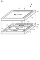
- FIG. 4 is an exploded perspective view showing an outline of a stack type chip structure of the CMOS image sensor 1.
- the laminated chip structure has a structure in which at least two semiconductor substrates of a pixel chip 41 which is a first substrate and a logic chip 42 which is a second substrate are laminated. ..
- each pixel 2 of the pixel array section 11, pixel control lines 31 1 to 31 m , and vertical signal lines 32 1 to 32 n are formed in the pixel chip 41 of the first layer.
- the second-layer logic chip 42 includes a row selection unit 12, a constant current source unit 13, an analog-digital conversion unit 14, a horizontal transfer scanning unit 15, a signal processing unit 16, a timing control unit (TG) 17, and a reference.
- a pixel controller including the signal generator 19 and the like for controlling the pixel 2 is formed.
- the pixel control unit is a peripheral circuit unit of the pixel array unit 11.
- the first-layer pixel chip 41 and the second-layer logic chip 42 are electrically connected to each other via bumps, TCV (Through Chip Via), and Cu-Cu hybrid bonding connecting portions 43 and 44. ..
- the size (area) of the pixel chip 41 of the first layer is sufficient to form the pixel array section 11. Therefore, the size (area) of the pixel chip 41, The size of the entire chip can be reduced. Further, a process suitable for manufacturing the pixel 2 can be applied to the first layer pixel chip 41, and a process suitable for manufacturing the pixel control unit (logic) can be applied to the second layer logic chip 42. In manufacturing the CMOS image sensor 1, there is also an advantage that the process can be optimized. In particular, when manufacturing the pixel control unit on the logic chip 42, it is possible to apply a tip miniaturization process.
- the laminated structure of the two-layer structure in which the pixel chip 41 and the logic chip 42 are laminated is illustrated, but the laminated structure is not limited to the two-layer structure, and may be a structure of three or more layers. You can also In the case of a stacked structure of three layers or more, the row selection unit 12, the constant current source unit 13, the analog-digital conversion unit 14, the horizontal transfer scanning unit 15, the signal processing unit 16, the timing control unit 17, and the reference signal generation.
- the pixel control section including the section 19 and the like can be dispersedly formed on the semiconductor substrate of the second and subsequent layers.
- a laminated chip having a three-dimensional structure in which a pixel chip 41 having the pixel array section 11 and a logic chip 42 having the pixel control section are bonded together
- the pixel chip 41 and the logic In general, a case where a non-defective product or a defective product is selected in an inspection in a wafer state which is a final shape after the chips 42 are bonded together.
- Lamination methods for laminated chips include a method of bonding wafers to each other (WOW: Wafer On Wafer) and a method of bonding wafers to non-defective chips (COW: Chip On Wafer).
- WOW Wafer On Wafer
- COW Chip On Wafer
- the pixel chip 41 on which the pixel array unit 11 is mounted and the pixel control unit (logic) such as the row selection unit 12 and the analog-digital conversion unit 14 are provided.
- the logic chips 42 to be mounted are manufactured by separate wafer processes. After that, the logic chip 42 is diced, and the logic chip 42 after dicing is attached to the pixel chip 41 in the wafer state.
- the first advantage of the COW type laminated structure is that each of the pixel chip 41 and the logic chip 42 can be manufactured by an optimized process.
- the pixel chip 41 it is possible to use a process optimized with respect to pixel characteristics such as a white spot and the maximum charge amount Q s.
- the logic chip 42 it is possible to increase the speed by using a fine process at the tip. Therefore, power saving can be achieved.
- the second advantage is that, as shown in FIG. 6, for each of the pixel chip 41 and the logic chip 42, non-defective products are selected before the bonding, and non-defective chips are bonded together, thereby preventing wasteful yield loss. Therefore, the cost can be reduced. Particularly in a large-sized sensor having a large area, when the yield of the pixel / logic single chip is not high, the effect of cost reduction by the selection of good products / defective products is great.
- the circuit configuration of the pixel array unit 11 mounted on the pixel chip 41 includes vertical signal lines 32 1 to 32 n in the column direction and pixel control lines 31 1 to 31 m in the row direction.
- the wiring is stretched around.
- a short circuit (short circuit) / open (open circuit) defect occurs in these wirings, it causes a line defect in the output image of the image pickup device.
- These wiring defects are the main cause of chip defects.
- Detecting wiring shorts can be achieved relatively easily. For example, when a different potential is applied to the adjacent wirings from the outside and a leak current is observed between the adjacent wirings, it can be determined that a wiring short circuit has occurred somewhere.
- a plurality of wirings (here, vertical signal lines 32 1 to 32 n are illustrated) are switched elements (for example, MOS transistors) 45 1 to 45 i . They are connected in series to form one daisy chain (wiring chain). Then, when the selection of non-defective / defective, the test signal test_en a high level fixed, with the switch elements 45 1 ⁇ 45 i on, so as to provide both ends of daisy chain voltage V a, the V b. The test signal test_en and the voltages V a and V b are applied through the test pad 46.
- switched elements for example, MOS transistors
- the pixel control lines 31 1 to 31 m and the vertical signal lines 32 1 to 32 n usually have wiring resistance of about 10 k ⁇ per several lines, and in view of the current measurement accuracy (about nA),
- the maximum number of wires that can be connected in series with one daisy chain is several tens to several hundreds.
- the image pickup device having a stacked structure tends to have a higher defective rate of the wirings of the pixel control lines 31 1 to 31 m and the vertical signal lines 32 1 to 32 n than the defective rate of a single pixel for the purpose of increasing the number of pixels and increasing the speed. It is in. Therefore, in the embodiment of the present disclosure, in the pixel chip 41 in which the pixel array unit 11 is formed, the main purpose is to check only the wiring layer, and the minimum circuits are added, whereby the pixel control lines 31 1 to 31 m are added. It is possible to detect wiring failure of the vertical signal lines 32 1 to 32 n , specifically, open failure (disconnection).
- all wiring is divided into a plurality of daisy chains (wiring chains), and all of the divided daisy chains have an open defect.
- the detection (sorting) is performed in parallel (simultaneously). As a result, it is possible to shorten the time required to detect a wiring defect (that is, an open defect). Further, since the number of constituent elements (for example, transistors) and test terminals (test pads) of the circuit for detecting the open defect can be reduced, the area overhead can be reduced.
- Example 1 is a basic configuration example of the pixel chip 41 according to the embodiment of the present disclosure.
- FIG. 8 shows an example of the basic configuration of the pixel chip 41 according to the first embodiment.
- the open defects of the wirings arranged in the upper, lower, left, and right of the pixel array unit 11 are detected (sorted).
- the defect detection circuits 47A to 47D for carrying out) are mounted.
- the defect detection circuits 47A and 47B arranged above and below the pixel array section 11 are for detecting wiring defects of the vertical signal lines 32 1 to 32 n wired along the pixel columns.
- the defect detection circuits 47C and 47D arranged on the left and right of the pixel array unit 11 are for detecting wiring defects of the pixel control lines 31 1 to 31 m wired along the pixel rows.
- the pixel chip 41 is electrically connected to the logic chip 42 (see FIG. 5) via the connecting portions 43A and 43B and the connecting portions 44A and 44B arranged on the peripheral portion thereof.
- the connecting portions 43A and 43B and the connecting portions 44A and 44B are formed of bumps, TCVs, Cu-Cu hybrid bonding and the like.
- pad portions 48A to 48D for inspecting (selecting) non-defective products / defective products are provided in the peripheral portion of the pixel chip 41, corresponding to the defect detection circuits 47A to 47D.
- Example 2 is a specific configuration example of the pixel chip 41 according to Example 1.
- FIG. 9 shows an example of a specific configuration of the pixel chip 41 according to the second embodiment.
- the pixel array section 11 is divided into a plurality of (p) regions in the row direction, and the divided regions are pixel blocks 51 1 to 51 p . Then, for the vertical signal lines 32 1 to 32 n wired along the pixel columns, one daisy chain is formed for each of the pixel blocks 51 1 to 51 p . The details will be described later.
- the defect detection circuit 47A has three connection wirings 52 1 , 52 2 , and 52 3 arranged along the row direction.
- the pixel blocks 51 1 to 51 p of the pixel array section 11 are connected to the test pads 53 1 , 53 2 , 53 3 of the pad section 48A through three connection wirings 52 1 , 52 2 , 52 3 , respectively. ..
- the test signal test_en is applied to the test pad 53 1 , and the connection wiring 52 1 transmits the test signal test_en in the row direction.
- the test pad 53 2 the first voltage V a is applied, the first voltage V a, the connection wiring 52 2, which is the first wiring is transmitted to the row direction.
- the test pad 53 3, the second voltage V b is applied, the second voltage V b, the second a wiring which connection wiring 52 3 is transmitted to the row direction.
- the defect detection circuit 47B has three connection wirings 52 4 , 52 5 , 52 6 arranged along the row direction.
- the pixel blocks 51 1 to 51 p of the pixel array section 11 are connected to the test pads 53 4 , 53 5 , 53 6 of the pad section 48B through three connection wirings 52 4 , 52 5 , 52 6 , respectively. ..
- the test signal test_en is applied to the test pad 53 4 , and the connection wiring 52 4 transmits the test signal test_en in the row direction.
- a third voltage V c is applied to the test pad 53 5 , and the third wiring V 5 that is the third wiring transmits this third voltage V c in the row direction.
- the test pad 53 6, the fourth voltage V d is applied, the fourth voltage V d, the fourth connection wiring 52 6 are wires are transferred to the row direction.
- FIG. 10 shows an example of a daisy chain in one pixel block of the pixel array section 11 and a circuit configuration of the two defect detection circuits 47A and 47B.
- the pixel block 51 1 will be described as an example, but other pixel blocks 51 2 to 51 p have the same configuration.
- j vertical signal lines 32 1 to 32 j of the pixel block 51 1 are denoted by vsl # 1 to vsl # j.
- the j vertical signal lines vsl # 1 to vsl # j of the pixel block 51 1 are connected in series by the switch element groups at both ends to form one daisy chain.
- each switch element eg, MOS transistor
- the gate electrodes (gate terminals) of the switch transistors s 1 to s j are connected to the test pads 53 1 and 53 4 via connection wirings 52 1 and 52 4 .
- a high-level test signal test_en is applied through the test pads 53 1 and 53 4 and the connection wirings 52 1 and 52 4 to turn it on to form a daisy chain.
- the switch transistor s 1 corresponding to the first run of the vertical signal lines vsl # 1 the first voltage V a is applied through the connection wiring 52 2, switching transistors corresponding to the vertical signal line vsl # j of j-th s j
- a second voltage V b is applied to the terminal through the connection wiring 52 3 . Then, by applying the high-level test signal test_en, the first voltage V a , and the second voltage V b , it is possible to detect (select) an open defect of the vertical signal lines vsl # 1 to vsl # j. It will be possible.
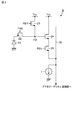
- Failure detection circuit 47B is connected wires 52 4, 52 5, 52 6 and the switch transistors s 2, s 4, ⁇ ⁇ ⁇ , in addition to s j, the switch transistors Tr 1 and a first switching element , And a switch transistor Tr 2 which is a second switch element.
- the switch transistor Tr 1 has a gate electrode connected to the test pad 53 4 via a connection wiring 52 4 and a drain electrode connected to an intermediate position V m of the daisy chain.
- the source electrode is connected to the test pad 53 5 via the connection wiring 52 5
- the drain electrode is connected to the test pad 53 6 via the connection wiring 52 6
- the gate electrode is connected to the switch transistor Tr 1 . It is connected to the source electrode.
- Each of the switch transistors s 1 to s j of the defect detection circuits 47A and 47B and the switch transistors Tr 1 and 2 of the defect detection circuit 47B should be composed of transistors of the same conductivity type as the transistors forming the pixel 2.
- the pixel 2 is configured on the pixel chip 41 side by only N-channel MOS transistors as shown in FIG. 2 by optimizing the area efficiency and the process reduction viewpoint.
- the switch transistors s 1 to s j and the switch transistors Tr 1 and Tr 2 are also configured by using N-channel MOS transistors of the same type as the pixel 2. This eliminates the need to add a new element type (that is, a new process step) from the existing pixel process.
- the failure detection circuit 47A, 47B of the above construction when the open defect detection (when the selection of non-defective / defective), the test pad 53 1, 53 4, applies a test signal test_en high level, the first Voltage V a / second voltage V b / third voltage V c / fourth voltage V d , a predetermined voltage value is applied. Then, in this state, whether or not an open defect (disconnection defect) has occurred in the vertical signal lines 32 1 to 32 n is observed by observing whether or not a short current is generated between the test pads 53 5 and 53 6. It is possible to make a determination in pixel block units.
- V th is the threshold voltage of the switch transistors s 1 to s j and the switch transistors Tr 1 and Tr 2 .
- test signal test_en and the third voltage V c / fourth voltage V d sets the voltage value V DD2 / voltage V DD3 / voltage value V DD4.
- the voltage values of the test signal test_en and the third voltage V c / the fourth voltage V d are common to the setting a and the setting b.
- the switch transistors s 1 to s j and the switch transistors Tr 1 and Tr 2 are turned on, the vertical signal lines vsl # 1 to vsl # j are electrically connected to each other in series, and one daisy A chain is constructed.
- FIG. 11B shows case classification that occurs when an open defect is detected.
- a voltage value V DD3 higher than the voltage value V DD1 / 2 + V th is set as the third voltage V c
- a fourth voltage V d is higher than the voltage value V DD3. to set the high voltage value V DD4 (V DD3 ⁇ V DD4 ).
- Case (1) is a case where no open failure occurs in the vertical signal lines vsl # 1 to vsl # j in the daisy chain.
- the potential at the intermediate position V m of the daisy chain becomes 1 ⁇ 2 of the voltage value V DD1 .
- the potential at the intermediate position V m is input to the gate electrode of the switch transistor Tr 2 via the switch transistor Tr 1 .
- the switch transistor Tr 2 is turned off because the gate voltage is lower than the source / drain voltage. Therefore, in case (1), no short-circuit current is generated between the test pads 53 5 and 53 6 .
- the switch transistor Tr 2 in the setting b is turned on by the condition (3) _2 in the table of FIG. 11A.
- the test pad 53 5, 53 between 6, short path is formed through the connection wiring 52 5, 52 6, the short current is generated.
- the switch transistor Tr 2 is turned off, so that no short circuit current is generated between the test pads 53 5 and 53 6 .
- the switching transistor Tr 2 in setting b since the switching transistor Tr 2 in setting b is turned on, the test pad 53 5, 53 between 6, short path is formed through the connection wiring 52 5, 52 6, the short current is generated. In the setting a, the switch transistor Tr 2 is turned off, so that no short circuit current is generated between the test pads 53 5 and 53 6 .
- Case (4) is the case where the open failure occurs in both the vertical signal lines vsl # 1 to vsl # j / 2 and the vertical signal lines vsl # (j / 2 + 1) to vsl # j.
- the potential of the intermediate position V m of the daisy chain of the settings a and b is indefinite. If the switch transistor Tr 2 happens to be turned on in both settings a and b, the open failure is not detected.
- the defect using the image after the pixel chip 41 and the logic chip 42 are bonded can be selected as a line defect, and thus the defective chip is not detected. Will not be leaked. Since the occurrence probability of the case (4) is lower than that of the cases (2) and (3), the yield of bonded chips due to the omission of selection of the pixel chip 41 alone and the cost effect due to deterioration of the selection time are small.
- the weak leak current described above is specifically the gate leak of the transistors connected to the pixel control lines 31 1 to 31 m and the selection transistor connected to the vertical signal lines 32 1 to 32 n (see FIG. 2). Source / drain leak of the selection transistor 25).
- the threshold voltage of the N-channel MOS transistor As shown in conditions (2) / (3) of applied voltage in the table of FIG. 11A, it is necessary to consider the threshold voltage of the N-channel MOS transistor as the applied voltage at the time of selection. If the variation in the threshold voltage of the N-channel MOS transistor is large, the constraint cannot be satisfied, which may adversely affect the sorting accuracy. When there is a large variation in the threshold voltage between lots / wafers / chips, the threshold voltage of the pixel transistor is acquired in advance using well-known technology, and the applied voltage at the time of sorting is dynamically adjusted using that information. By doing so, the influence of variations can be suppressed and the robustness of sorting can be improved.
- the switch transistors s 1 to s j and the switch transistors Tr 1 and Tr 2 are turned off, and the daisy chain is not configured. Specifically, by controlling the test signal test_en from the outside of the sensor so that the test signal test_en becomes the ground level (or a voltage lower than the threshold voltage V th ) or by attaching a resistor inside the chip, During operation, the switch transistors s 1 to s j and the switch transistors Tr 1 and Tr 2 can be turned off. Similar processing may be performed on each voltage value of the first voltage V a / second voltage V b / third voltage V c / fourth voltage V d as necessary.
- FIG. 13 shows an example of a method for preventing erroneous detection of disconnection due to the leak current.
- one ends of the wirings SEL_1 to SEL_m for applying the selection signal SEL to the selection transistor 25 of each pixel are connected to the test pad 53 7 via the switch transistors s 11 to s 1m .
- the test pad 53 7, sufficiently low voltage V e enough to the selection transistor 25 in the OFF state is applied from the outside.
- a high-level test signal test_en is applied to each gate electrode of the switch transistors s 11 to s 1m via the test pad 53 8 .
- the switch transistors s 11 ⁇ s 1 m is turned on, sufficiently low
- the voltage V e is applied to the gate electrode of the selection transistor 25 of each pixel via the wirings SEL _1 to SEL _m .
- the selection transistor 25 is turned off, and the leak current does not flow. Therefore, it is possible to prevent erroneous detection of disconnection due to the leak current.
- the pixel control lines 31 1 to 31 m of the pixel array section 11 are connected only to the gate electrodes of the pixel transistors (the transfer transistor 22, the reset transistor 23, and the selection transistor 25), so that the above leak path is not generated. Does not occur.
- the technique according to the present disclosure is limited to the application to the CMOS image sensor. Not a thing. That is, the technique according to the present disclosure can be applied to all XY addressing type image pickup devices in which pixels 2 are two-dimensionally arranged in a matrix.
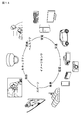
- the imaging device according to the present embodiment described above can be used in various devices that sense light such as visible light, infrared light, ultraviolet light, and X-rays, as shown in FIG. 14, for example. Specific examples of various devices are listed below.
- -A device that captures images used for viewing, such as a digital camera or a portable device with a camera function.
- a digital camera or a portable device with a camera function for safe driving such as automatic stop, and recognition of the driver's condition.
- Devices used for traffic such as in-vehicle sensors that take images of the rear, surroundings, and inside the vehicle, surveillance cameras that monitor running vehicles and roads, ranging sensors that measure the distance between vehicles, etc.
- Devices used for home appliances such as TVs, refrigerators, and air conditioners in order to take images and operate the devices according to the gestures-Endoscopes, devices that perform blood vessel imaging by receiving infrared light, etc.
- Security devices such as security surveillance cameras and person authentication cameras
- Skin measuring devices for skin and scalp Beauty such as microscope
- Such action camera or wearable cameras provided by equipment and sports applications such as for the use, such as a camera for monitoring a sports state of the apparatus, groves and crops that are provided for use in, is provided for use in agricultural equipment
- the technology according to the present disclosure can be applied to various products. More specifically, it can be applied to an image pickup system such as a digital still camera or a video camera, a mobile terminal device having an image pickup function such as a mobile phone, or an electronic device such as a copying machine using an image pickup device in an image reading unit. it can.
- an image pickup system such as a digital still camera or a video camera
- a mobile terminal device having an image pickup function such as a mobile phone
- an electronic device such as a copying machine using an image pickup device in an image reading unit.
- an imaging system such as a digital still camera or a video camera
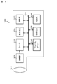
- FIG. 15 is a block diagram showing a configuration of an imaging system which is an example of the electronic device of the present disclosure.
- the imaging system 100 includes an imaging optical system 101 including a lens group, an imaging unit 102, a DSP (Digital Signal Processor) circuit 103, a frame memory 104, a display device 105, and a recording device 106.
- the DSP circuit 103, the frame memory 104, the display device 105, the recording device 106, the operation system 107, and the power supply system 108 are connected to each other via a bus line 109.
- the imaging optical system 101 captures incident light (image light) from a subject and forms an image on the imaging surface of the imaging unit 102.
- the image capturing unit 102 converts the light amount of the incident light imaged on the image capturing surface by the optical system 101 into an electric signal for each pixel and outputs the electric signal as a pixel signal.
- the DSP circuit 103 performs general camera signal processing, such as white balance processing, demosaic processing, and gamma correction processing.
- the frame memory 104 is used to appropriately store data in the process of signal processing in the DSP circuit 103.
- the display device 105 includes a panel-type display device such as a liquid crystal display device and an organic EL (electroluminescence) display device, and displays a moving image or a still image captured by the image capturing unit 102.
- the recording device 106 records the moving image or the still image captured by the image capturing unit 102 on a recording medium such as a portable semiconductor memory, an optical disc, or an HDD (Hard Disk Drive).
- the operation system 107 issues operation commands for various functions of the imaging system 100 under the operation of the user.
- the power supply system 108 appropriately supplies various power supplies serving as operating power supplies of the DSP circuit 103, the frame memory 104, the display device 105, the recording device 106, and the operation system 107 to these supply targets.
- the imaging device according to the above-described embodiment can be used as the imaging unit 102.
- the image pickup device the wiring formed for each pixel row or each pixel column can be inspected with a minimum of additional circuits, so that an increase in chip area can be suppressed. Therefore, by using the image pickup apparatus according to the above-described embodiment as the image pickup unit 102, it is possible to contribute to suppressing the size increase of the image pickup system 100.
- the technology according to the present disclosure (this technology) can be applied to various products.
- the technology according to the present disclosure may be applied to an endoscopic surgery system.
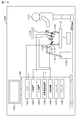
- FIG. 16 is a diagram showing an example of a schematic configuration of an endoscopic surgery system to which the technology according to the present disclosure (the present technology) can be applied.
- FIG. 16 illustrates a situation in which an operator (doctor) 11131 is operating on a patient 11132 on a patient bed 11133 using the endoscopic surgery system 11000.
- the endoscopic surgery system 11000 includes an endoscope 11100, other surgical tools 11110 such as a pneumoperitoneum tube 11111 and an energy treatment tool 11112, and a support arm device 11120 that supports the endoscope 11100.
- a cart 11200 on which various devices for endoscopic surgery are mounted.
- the endoscope 11100 includes a lens barrel 11101 into which a region of a predetermined length from the distal end is inserted into the body cavity of the patient 11132, and a camera head 11102 connected to the base end of the lens barrel 11101.
- the endoscope 11100 configured as a so-called rigid endoscope having the rigid barrel 11101 is illustrated, but the endoscope 11100 may be configured as a so-called flexible mirror having a flexible barrel. Good.
- An opening in which an objective lens is fitted is provided at the tip of the lens barrel 11101.
- a light source device 11203 is connected to the endoscope 11100, and the light generated by the light source device 11203 is guided to the tip of the lens barrel by a light guide extending inside the lens barrel 11101. It is irradiated toward the observation target in the body cavity of the patient 11132 via the lens.
- the endoscope 11100 may be a direct-viewing endoscope, or may be a perspective or side-viewing endoscope.
- An optical system and an image pickup device are provided inside the camera head 11102, and the reflected light (observation light) from the observation target is condensed on the image pickup device by the optical system.
- the observation light is photoelectrically converted by the imaging element, and an electric signal corresponding to the observation light, that is, an image signal corresponding to the observation image is generated.
- the image signal is transmitted to the camera control unit (CCU: Camera Control Unit) 11201 as RAW data.
- the CCU 11201 is composed of a CPU (Central Processing Unit), a GPU (Graphics Processing Unit), and the like, and controls the operations of the endoscope 11100 and the display device 11202 in a centralized manner. Further, the CCU 11201 receives the image signal from the camera head 11102, and performs various image processing such as development processing (demosaic processing) on the image signal for displaying an image based on the image signal.
- image processing such as development processing (demosaic processing)
- the display device 11202 displays an image based on the image signal subjected to the image processing by the CCU 11201 under the control of the CCU 11201.
- the light source device 11203 is composed of a light source such as an LED (Light Emitting Diode), for example, and supplies the endoscope 11100 with irradiation light when photographing a surgical site or the like.
- a light source such as an LED (Light Emitting Diode), for example, and supplies the endoscope 11100 with irradiation light when photographing a surgical site or the like.
- the input device 11204 is an input interface for the endoscopic surgery system 11000.
- the user can input various kinds of information and instructions to the endoscopic surgery system 11000 via the input device 11204.
- the user inputs an instruction to change the imaging conditions (type of irradiation light, magnification, focal length, etc.) by the endoscope 11100.
- the treatment instrument control device 11205 controls driving of the energy treatment instrument 11112 for cauterization of tissue, incision, sealing of blood vessel, or the like.
- the pneumoperitoneum device 11206 is used to inflate the body cavity of the patient 11132 through the pneumoperitoneum tube 11111 in order to inflate the body cavity of the patient 11132 for the purpose of securing the visual field by the endoscope 11100 and the working space of the operator.
- the recorder 11207 is a device capable of recording various information regarding surgery.
- the printer 11208 is a device capable of printing various information regarding surgery in various formats such as text, images, and graphs.
- the light source device 11203 that supplies irradiation light to the endoscope 11100 when imaging a surgical site can be configured by, for example, an LED, a laser light source, or a white light source configured by a combination thereof.
- a white light source is formed by a combination of RGB laser light sources
- the output intensity and output timing of each color (each wavelength) can be controlled with high accuracy, so that the light source device 11203 adjusts the white balance of the captured image. It can be carried out.
- the laser light from each of the RGB laser light sources is time-divided to the observation target, and the drive of the image pickup device of the camera head 11102 is controlled in synchronization with the irradiation timing, so that each of the RGB colors can be handled. It is also possible to take the captured image in time division. According to this method, a color image can be obtained without providing a color filter on the image sensor.
- the drive of the light source device 11203 may be controlled so as to change the intensity of the output light at predetermined time intervals.
- the drive of the image sensor of the camera head 11102 in synchronization with the timing of changing the intensity of the light to acquire an image in a time-division manner and synthesizing the images, a high dynamic without so-called blackout and whiteout. Images of the range can be generated.
- the light source device 11203 may be configured to be able to supply light in a predetermined wavelength band corresponding to special light observation.
- the special light observation for example, the wavelength dependence of the absorption of light in body tissues is used to irradiate a narrow band of light as compared with the irradiation light (that is, white light) at the time of normal observation, so that the mucosal surface
- the so-called narrow band imaging is performed in which a predetermined tissue such as blood vessels is imaged with high contrast.
- fluorescence observation in which an image is obtained by fluorescence generated by irradiating the excitation light may be performed.
- the body tissue is irradiated with excitation light to observe the fluorescence from the body tissue (autofluorescence observation), or a reagent such as indocyanine green (ICG) is locally injected into the body tissue and the body tissue is also injected.
- the excitation light corresponding to the fluorescence wavelength of the reagent can be irradiated to obtain a fluorescence image and the like.
- the light source device 11203 can be configured to be capable of supplying narrowband light and / or excitation light compatible with such special light observation.
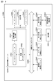
- FIG. 17 is a block diagram showing an example of the functional configuration of the camera head 11102 and the CCU 11201 shown in FIG.
- the camera head 11102 includes a lens unit 11401, an imaging unit 11402, a driving unit 11403, a communication unit 11404, and a camera head control unit 11405.
- the CCU 11201 has a communication unit 11411, an image processing unit 11412, and a control unit 11413.
- the camera head 11102 and the CCU 11201 are communicably connected to each other via a transmission cable 11400.
- the lens unit 11401 is an optical system provided at the connecting portion with the lens barrel 11101.
- the observation light taken in from the tip of the lens barrel 11101 is guided to the camera head 11102 and enters the lens unit 11401.
- the lens unit 11401 is configured by combining a plurality of lenses including a zoom lens and a focus lens.
- the image pickup unit 11402 is composed of an image pickup element.
- the number of image pickup elements forming the image pickup section 11402 may be one (so-called single-plate type) or plural (so-called multi-plate type).
- image signals corresponding to RGB are generated by each image pickup element, and a color image may be obtained by combining them.
- the image capturing unit 11402 may be configured to have a pair of image capturing elements for respectively acquiring the image signals for the right eye and the left eye corresponding to 3D (Dimensional) display.
- the 3D display enables the operator 11131 to more accurately understand the depth of the living tissue in the operation site.
- a plurality of lens units 11401 may be provided corresponding to each image pickup element.
- the image pickup unit 11402 does not necessarily have to be provided in the camera head 11102.
- the imaging unit 11402 may be provided inside the lens barrel 11101 immediately after the objective lens.
- the drive unit 11403 is composed of an actuator, and moves the zoom lens and the focus lens of the lens unit 11401 by a predetermined distance along the optical axis under the control of the camera head control unit 11405. Accordingly, the magnification and focus of the image captured by the image capturing unit 11402 can be adjusted appropriately.
- the communication unit 11404 is composed of a communication device for transmitting and receiving various information to and from the CCU11201.
- the communication unit 11404 transmits the image signal obtained from the imaging unit 11402 as RAW data to the CCU 11201 via the transmission cable 11400.
- the communication unit 11404 receives a control signal for controlling the driving of the camera head 11102 from the CCU 11201 and supplies it to the camera head control unit 11405.
- the control signal includes, for example, information that specifies the frame rate of the captured image, information that specifies the exposure value at the time of capturing, and / or information that specifies the magnification and focus of the captured image. Contains information about the condition.
- the image capturing conditions such as the frame rate, the exposure value, the magnification, and the focus may be appropriately designated by the user, or may be automatically set by the control unit 11413 of the CCU 11201 based on the acquired image signal. Good. In the latter case, the so-called AE (Auto Exposure) function, AF (Auto Focus) function, and AWB (Auto White Balance) function are mounted on the endoscope 11100.
- the camera head control unit 11405 controls driving of the camera head 11102 based on a control signal from the CCU 11201 received via the communication unit 11404.
- the communication unit 11411 is composed of a communication device for transmitting and receiving various information to and from the camera head 11102.
- the communication unit 11411 receives the image signal transmitted from the camera head 11102 via the transmission cable 11400.
- the communication unit 11411 transmits a control signal for controlling the driving of the camera head 11102 to the camera head 11102.
- the image signal and the control signal can be transmitted by electric communication, optical communication, or the like.
- the image processing unit 11412 performs various types of image processing on the image signal that is the RAW data transmitted from the camera head 11102.
- the control unit 11413 performs various controls regarding imaging of a surgical site or the like by the endoscope 11100 and display of a captured image obtained by imaging the surgical site or the like. For example, the control unit 11413 generates a control signal for controlling the driving of the camera head 11102.
- control unit 11413 causes the display device 11202 to display a captured image of the surgical site or the like based on the image signal subjected to the image processing by the image processing unit 11412.
- the control unit 11413 may recognize various objects in the captured image using various image recognition techniques.
- the control unit 11413 detects a surgical instrument such as forceps, a specific living body part, bleeding, and a mist when the energy treatment instrument 11112 is used by detecting the shape and color of the edge of the object included in the captured image. Can be recognized.
- the control unit 11413 may use the recognition result to superimpose and display various types of surgery support information on the image of the operation unit. By displaying the surgery support information in a superimposed manner and presenting it to the operator 11131, the burden on the operator 11131 can be reduced, and the operator 11131 can proceed with the operation reliably.
- the transmission cable 11400 that connects the camera head 11102 and the CCU 11201 is an electric signal cable compatible with electric signal communication, an optical fiber compatible with optical communication, or a composite cable of these.
- wired communication is performed using the transmission cable 11400, but communication between the camera head 11102 and the CCU 11201 may be performed wirelessly.
- the technology according to the present disclosure can be applied to, for example, the imaging unit 11402 of the camera head 11102 among the configurations described above.
- the technique according to the present disclosure to the imaging unit 11402 of the camera head 11102, the wiring formed in each pixel row or each pixel column can be inspected with a minimum of additional circuits, so that the chip area is increased. Can be suppressed, and as a result, an increase in the chip area can be suppressed, which can contribute to the suppression of upsizing of the imaging unit 11402 of the camera head 11102.
- the technology according to the present disclosure (this technology) can be applied to various products in addition to the endoscopic surgery system.
- the technology according to the present disclosure can be applied to any type of movement such as an automobile, an electric vehicle, a hybrid electric vehicle, a motorcycle, a bicycle, a personal mobility, an airplane, a drone, a ship, a robot, a construction machine, and an agricultural machine (tractor). It may be realized as an image sensor mounted on the body.
- FIG. 18 is a block diagram showing a schematic configuration example of a vehicle control system which is an example of a mobile body control system to which the technology according to the present disclosure can be applied.
- the vehicle control system 12000 includes a plurality of electronic control units connected via a communication network 12001.
- the vehicle control system 12000 includes a drive system control unit 12010, a body system control unit 12020, a vehicle exterior information detection unit 12030, a vehicle interior information detection unit 12040, and an integrated control unit 12050.
- a microcomputer 12051, an audio / video output unit 12052, and an in-vehicle network I / F (interface) 12053 are illustrated as a functional configuration of the integrated control unit 12050.
- the drive system control unit 12010 controls the operation of devices related to the drive system of the vehicle according to various programs.
- the drive system control unit 12010 includes a drive force generation device for generating a drive force of a vehicle such as an internal combustion engine or a drive motor, a drive force transmission mechanism for transmitting the drive force to wheels, and a steering angle of the vehicle. It functions as a steering mechanism for adjusting and a control device such as a braking device for generating a braking force of the vehicle.
- the body system control unit 12020 controls the operation of various devices mounted on the vehicle body according to various programs.
- the body system control unit 12020 functions as a keyless entry system, a smart key system, a power window device, or a control device for various lamps such as a head lamp, a back lamp, a brake lamp, a winker, or a fog lamp.
- the body system control unit 12020 can be input with radio waves or signals of various switches transmitted from a portable device that substitutes for a key.
- the body system control unit 12020 receives input of these radio waves or signals and controls the vehicle door lock device, power window device, lamp, and the like.
- the vehicle exterior information detection unit 12030 detects information outside the vehicle equipped with the vehicle control system 12000.
- the image pickup unit 12031 is connected to the vehicle exterior information detection unit 12030.
- the vehicle exterior information detection unit 12030 causes the image capturing unit 12031 to capture an image of the vehicle exterior and receives the captured image.
- the vehicle exterior information detection unit 12030 may perform object detection processing or distance detection processing such as people, vehicles, obstacles, signs, or characters on the road surface based on the received image.
- the image pickup unit 12031 is an optical sensor that receives light and outputs an electric signal according to the amount of received light.
- the imaging unit 12031 can output the electric signal as an image or as distance measurement information.
- the light received by the imaging unit 12031 may be visible light or invisible light such as infrared light.
- the in-vehicle information detection unit 12040 detects in-vehicle information.
- a driver state detection unit 12041 that detects the state of the driver is connected.
- the driver state detection unit 12041 includes, for example, a camera that images the driver, and the in-vehicle information detection unit 12040 determines the degree of fatigue or concentration of the driver based on the detection information input from the driver state detection unit 12041. It may be calculated or it may be determined whether or not the driver is asleep.
- the microcomputer 12051 calculates the control target value of the driving force generation device, the steering mechanism or the braking device based on the information on the inside and outside of the vehicle acquired by the outside information detection unit 12030 or the inside information detection unit 12040, and the drive system control unit.
- a control command can be output to 12010.
- the microcomputer 12051 realizes a function of ADAS (Advanced Driver Assistance System) that includes collision avoidance or impact mitigation of a vehicle, follow-up traveling based on an inter-vehicle distance, vehicle speed maintenance traveling, a vehicle collision warning, or a vehicle lane departure warning. It is possible to perform cooperative control for the purpose.
- ADAS Advanced Driver Assistance System
- the microcomputer 12051 controls the driving force generation device, the steering mechanism, the braking device, or the like on the basis of the information around the vehicle acquired by the vehicle exterior information detection unit 12030 or the vehicle interior information detection unit 12040, so that the driver's It is possible to perform cooperative control for the purpose of autonomous driving or the like that autonomously travels without depending on the operation.
- the microcomputer 12051 can output a control command to the body system control unit 12020 based on the information outside the vehicle acquired by the outside information detection unit 12030.
- the microcomputer 12051 controls the headlamp according to the position of the preceding vehicle or the oncoming vehicle detected by the vehicle exterior information detection unit 12030, and performs cooperative control for the purpose of antiglare such as switching the high beam to the low beam. It can be carried out.
- the voice image output unit 12052 transmits an output signal of at least one of a voice and an image to an output device capable of visually or audibly notifying information to an occupant of the vehicle or the outside of the vehicle.
- an audio speaker 12061, a display unit 12062, and an instrument panel 12063 are illustrated as output devices.
- the display unit 12062 may include at least one of an on-board display and a head-up display, for example.
- FIG. 19 is a diagram showing an example of the installation position of the imaging unit 12031.
- the vehicle 12100 has imaging units 12101, 12102, 12103, 12104, 12105 as the imaging unit 12031.
- the imaging units 12101, 12102, 12103, 12104, 12105 are provided at positions such as the front nose of the vehicle 12100, the side mirrors, the rear bumper, the back door, and the upper part of the windshield inside the vehicle.
- the image capturing unit 12101 provided on the front nose and the image capturing unit 12105 provided on the upper part of the windshield in the vehicle interior mainly acquire images in front of the vehicle 12100.
- the imaging units 12102 and 12103 included in the side mirrors mainly acquire images of the side of the vehicle 12100.
- the image capturing unit 12104 provided in the rear bumper or the back door mainly acquires an image behind the vehicle 12100.
- the front images acquired by the image capturing units 12101 and 12105 are mainly used for detecting a preceding vehicle, a pedestrian, an obstacle, a traffic signal, a traffic sign, a lane, or the like.
- FIG. 19 shows an example of the shooting range of the imaging units 12101 to 12104.
- the imaging range 12111 indicates the imaging range of the imaging unit 12101 provided on the front nose
- the imaging ranges 12112 and 12113 indicate the imaging ranges of the imaging units 12102 and 12103 provided on the side mirrors
- the imaging range 12114 indicates The imaging range of the imaging part 12104 provided in a rear bumper or a back door is shown. For example, by overlaying the image data captured by the image capturing units 12101 to 12104, a bird's-eye view image of the vehicle 12100 viewed from above can be obtained.
- At least one of the imaging units 12101 to 12104 may have a function of acquiring distance information.
- at least one of the image capturing units 12101 to 12104 may be a stereo camera including a plurality of image capturing elements or may be an image capturing element having pixels for phase difference detection.
- the microcomputer 12051 based on the distance information obtained from the imaging units 12101 to 12104, the distance to each three-dimensional object in the imaging range 12111 to 12114 and the temporal change of this distance (relative speed with respect to the vehicle 12100). It is possible to extract the closest three-dimensional object on the traveling path of the vehicle 12100, which is traveling in a substantially same direction as the vehicle 12100 at a predetermined speed (for example, 0 km / h or more), as a preceding vehicle. it can. Further, the microcomputer 12051 can set an inter-vehicle distance to be secured in front of the preceding vehicle in advance, and can perform automatic braking control (including follow-up stop control), automatic acceleration control (including follow-up start control), and the like. In this way, it is possible to perform cooperative control for the purpose of autonomous driving, which autonomously travels without depending on the operation of the driver.
- automatic braking control including follow-up stop control
- automatic acceleration control including follow-up start control
- the microcomputer 12051 uses the distance information obtained from the image capturing units 12101 to 12104 to convert three-dimensional object data regarding a three-dimensional object to other three-dimensional objects such as two-wheeled vehicles, ordinary vehicles, large vehicles, pedestrians, telephone poles, and the like. It can be classified, extracted, and used for automatic avoidance of obstacles. For example, the microcomputer 12051 identifies an obstacle around the vehicle 12100 into an obstacle visible to the driver of the vehicle 12100 and an obstacle difficult to see. Then, the microcomputer 12051 determines the collision risk indicating the risk of collision with each obstacle, and when the collision risk is equal to or more than the set value and there is a possibility of collision, the microcomputer 12051 outputs the audio through the audio speaker 12061 and the display unit 12062. A driver can be assisted for avoiding a collision by outputting an alarm to the driver and performing forced deceleration or avoidance steering through the drive system control unit 12010.
- At least one of the imaging units 12101 to 12104 may be an infrared camera that detects infrared rays.
- the microcomputer 12051 can recognize the pedestrian by determining whether or not the pedestrian is present in the images captured by the imaging units 12101 to 12104. To recognize such a pedestrian, for example, a procedure of extracting a feature point in an image captured by the image capturing units 12101 to 12104 as an infrared camera and a pattern matching process on a series of feature points indicating the contour of an object are performed to determine whether the pedestrian is a pedestrian.
- the voice image output unit 12052 causes the recognized pedestrian to have a rectangular contour line for emphasis.
- the display unit 12062 is controlled so as to superimpose.
- the audio image output unit 12052 may control the display unit 12062 to display an icon indicating a pedestrian or the like at a desired position.
- the technology according to the present disclosure can be applied to, for example, the imaging unit 12031 or the like among the configurations described above.
- the technique according to the present disclosure to the imaging unit 12031 and the like, it is possible to inspect the wiring formed for each pixel row or each pixel column with a minimum of additional circuits, and thus it is possible to suppress an increase in chip area.
- the increase in the chip area can be suppressed, which can contribute to the suppression of the size increase of the imaging unit 12031 and the like.
- A. Imaging device ⁇ [A-1] A first substrate on which a pixel array part formed by arranging pixels including light receiving parts in a matrix is formed, and a second substrate on which a pixel control part for controlling pixels is formed are stacked. Consists of The first substrate is A first wiring transmitting a first voltage, A second wire for transmitting a second voltage, and When the pixel array section is divided into a plurality of pixel blocks in units of a plurality of pixel columns or a plurality of pixel rows, a defect detection circuit for detecting a wiring defect is provided for each pixel block, The defect detection circuit When a wiring defect is detected, a plurality of wirings corresponding to a plurality of pixel columns or a plurality of pixel rows are connected in series for each pixel block, and one end of a wiring chain connected in series in each pixel block is connected to the first wiring.
- the defect detection circuit is a switch that connects a plurality of wirings in series between the first wiring and the second wiring for each pixel block to form a wiring chain when a wiring failure is detected.
- the first substrate is A third wire for transmitting a third voltage, and Having a fourth wiring for transmitting a fourth voltage
- the defect detection circuit A first switch element that is connected to an intermediate position of the wiring chain and reads the potential at the intermediate position; and A second switch element that is connected between the third wiring and the fourth wiring and that performs an on / off operation in accordance with the potential at the intermediate position read through the first switch element;
- the imaging device according to [A-1] or [A-2].
- the defect detection circuit detects a wiring defect depending on whether or not a short-circuit current is generated between the third wiring and the fourth wiring.
- the imaging device according to the above [A-3].
- the defect detection circuit detects a wire disconnection defect between one end and an intermediate position of the wiring chain or a wire disconnection defect between the intermediate position and the other end of the wiring chain.
- Each switch element of the switch element group of the defect detection circuit, the first switch element, and the second switch element are transistors of the same conductivity type as the transistors forming the pixel.
- [A-7] When the transistor forming the pixel is an N-channel MOS transistor, Each switch element, the first switch element, and the second switch element of the switch element group of the defect detection circuit are composed of N-channel MOS transistors of the same kind as the pixel.
- a first substrate on which a pixel array unit formed by arranging pixels including light receiving units in a matrix is formed, and a second substrate on which a pixel control unit for controlling the pixels is formed are stacked.
- Consists of The first substrate is A first wiring transmitting a first voltage, A second wire for transmitting a second voltage, and
- a defect detection circuit for detecting a wiring defect is provided for each pixel block, The defect detection circuit
- a plurality of wirings corresponding to a plurality of pixel columns or a plurality of pixel rows are connected in series for each pixel block, and one end of a wiring chain connected in series in each pixel block is connected to the first wiring.
- the defect detection circuit is a switch that connects a plurality of wirings in series between each of the first wiring and the second wiring for each pixel block to form a wiring chain when a wiring failure is detected.
- the first substrate is A third wire for transmitting a third voltage, and Having a fourth wiring for transmitting a fourth voltage
- the defect detection circuit A first switch element that is connected to an intermediate position of the wiring chain and reads the potential at the intermediate position; and A second switch element that is connected between the third wiring and the fourth wiring and that performs an on / off operation according to the potential of the intermediate position read through the first switch element;
- the electronic device according to the above [B-1] or [B-2].
- the defect detection circuit detects a wiring defect depending on whether or not a short circuit current is generated between the third wiring and the fourth wiring.
- the defect detection circuit detects a wire disconnection defect between one end and an intermediate position of the wiring chain or a wire disconnection defect between the intermediate position and the other end of the wiring chain.
- Each of the switch elements, the first switch element, and the second switch element of the switch element group of the defect detection circuit are composed of a transistor of the same conductivity type as the transistor forming the pixel.
- [B-7] When the transistor forming the pixel is an N-channel MOS transistor,
- Each switch element, the first switch element, and the second switch element of the switch element group of the defect detection circuit are composed of N-channel MOS transistors of the same kind as the pixel.
- Logic chip (second substrate), 43 (43A, 43B), 44 (44A, 44B). ..Connection parts, 47A to 47D ... Detection circuit, 48A ⁇ 48D ... pad portion, 51 1 ⁇ 51 p ... pixel block, 52 1-52 6 ... connection wiring 53 1-53 8 ... test pad
Landscapes
- Engineering & Computer Science (AREA)
- Multimedia (AREA)
- Signal Processing (AREA)
- Health & Medical Sciences (AREA)
- Biomedical Technology (AREA)
- General Health & Medical Sciences (AREA)
- Physics & Mathematics (AREA)
- General Physics & Mathematics (AREA)
- Solid State Image Pick-Up Elements (AREA)
- Transforming Light Signals Into Electric Signals (AREA)
- Liquid Crystal Substances (AREA)
Abstract
受光部を含む画素が行列状に配置されて成る画素アレイ部が形成された第1の基板、及び、画素を制御する画素制御部が形成された第2の基板が積層されて成る。第1の基板は、第1の電圧を伝送する第1の配線、第2の電圧を伝送する第2の配線、及び、画素アレイ部を、複数の画素列又は複数の画素行を単位として複数の画素ブロックに分割したとき、画素ブロック毎に、配線不良の検出を行う不良検出回路を備える。不良検出回路は、配線不良の検出時に、画素ブロック毎に、複数の画素列又は複数の画素行に対応する複数の配線を直列に接続し、各画素ブロックの直列に接続された配線チェーンの一端を第1の配線に接続し、他端を第2の配線に接続し、配線チェーンの中間位置の電位に基づいて配線不良の検出を行う。
Description
本開示は、撮像装置及び電子機器に関する。
半導体基板上にマトリクス状に配置されて成る受光素子について、受光信号出力用の穿孔状電極が形成される以前の状態でも、検査を行うことができるようにした受光チップがある(例えば、特許文献1参照)。
特許文献1に記載の受光チップでは、複数の受光素子を幾つかの素子群に分割し、各素子群に対応して検査用パッドを設ける。そして、各素子群をそれぞれ共通の検査用信号線に接続し、各検査用パッドには、出力回路及び入力回路の双方を接続し、切替スイッチにより、検査用信号線を、対応する検査用パッドの出力回路又は入力回路の何れかに接続することで、検査用パッドを用いて受光素子の検査を可能にしている。
上記の特許文献1に記載の受光チップは、受光信号出力用の穿孔状電極が形成される以前の状態での、受光素子の検査を目的としてなされたものである。
本開示は、画素行毎あるいは画素列毎に形成された配線について、最小限の追加回路で検査を行うことができる撮像装置及び当該撮像装置を有する電子機器を提供することを目的とする。
上記の目的を達成するための本開示の撮像装置は、
受光部を含む画素が行列状に配置されて成る画素アレイ部が形成された第1の基板、及び、画素を制御する画素制御部が形成された第2の基板が積層されて成り、
第1の基板は、
第1の電圧を伝送する第1の配線、
第2の電圧を伝送する第2の配線、及び、
画素アレイ部を、複数の画素列又は複数の画素行を単位として複数の画素ブロックに分割したとき、画素ブロック毎に、配線不良の検出を行う不良検出回路を備え、
不良検出回路は、
配線不良の検出時に、画素ブロック毎に、複数の画素列又は複数の画素行に対応する複数の配線を直列に接続し、各画素ブロックの直列に接続された配線チェーンの一端を第1の配線に接続し、他端を第2の配線に接続し、
配線チェーンの中間位置の電位に基づいて配線不良の検出を行う。
受光部を含む画素が行列状に配置されて成る画素アレイ部が形成された第1の基板、及び、画素を制御する画素制御部が形成された第2の基板が積層されて成り、
第1の基板は、
第1の電圧を伝送する第1の配線、
第2の電圧を伝送する第2の配線、及び、
画素アレイ部を、複数の画素列又は複数の画素行を単位として複数の画素ブロックに分割したとき、画素ブロック毎に、配線不良の検出を行う不良検出回路を備え、
不良検出回路は、
配線不良の検出時に、画素ブロック毎に、複数の画素列又は複数の画素行に対応する複数の配線を直列に接続し、各画素ブロックの直列に接続された配線チェーンの一端を第1の配線に接続し、他端を第2の配線に接続し、
配線チェーンの中間位置の電位に基づいて配線不良の検出を行う。
また、上記の目的を達成するための本開示の電子機器は、上記の構成の撮像装置を有する。
以下、本開示の技術を実施するための形態(以下、「実施形態」と記述する)について図面を用いて詳細に説明する。本開示の技術は実施形態に限定されるものではない。以下の説明において、同一要素又は同一機能を有する要素には同一符号を用いることとし、重複する説明は省略する。尚、説明は以下の順序で行う。
1.本開示の撮像装置及び電子機器、全般に関する説明
2.本開示の撮像装置
2-1.CMOSイメージセンサの構成例
2-2.画素の構成例
2-3.アナログ-デジタル変換部の構成例
2-4.積層型のチップ構造
2-5.配線のショート/オープン不良について
3.実施形態の説明
3-1.実施例1(画素チップの基本的な構成例)
3-2.実施例2(実施例1に係る画素チップの具体的な構成例)
4.変形例
5.応用例
6.本開示に係る技術の適用例
6-1.本開示の電子機器(撮像システムの例)
6-2.内視鏡手術システムへの応用例
6-3.移動体への応用例
7.本開示がとることができる構成
1.本開示の撮像装置及び電子機器、全般に関する説明
2.本開示の撮像装置
2-1.CMOSイメージセンサの構成例
2-2.画素の構成例
2-3.アナログ-デジタル変換部の構成例
2-4.積層型のチップ構造
2-5.配線のショート/オープン不良について
3.実施形態の説明
3-1.実施例1(画素チップの基本的な構成例)
3-2.実施例2(実施例1に係る画素チップの具体的な構成例)
4.変形例
5.応用例
6.本開示に係る技術の適用例
6-1.本開示の電子機器(撮像システムの例)
6-2.内視鏡手術システムへの応用例
6-3.移動体への応用例
7.本開示がとることができる構成
<本開示の撮像装置及び電子機器、全般に関する説明>
本開示の撮像装置及び電子機器にあっては、不良検出回路について、配線不良の検出時に、第1の配線と第2の配線との間に、画素ブロック毎に、複数の配線を直列に接続して配線チェーンを構成するスイッチ素子群を有する構成とすることができる。このとき、スイッチ素子群の一方の端部のスイッチ素子が第1の配線に接続され、他方の端部のスイッチ素子が第2の配線に接続された構成とすることができる。
本開示の撮像装置及び電子機器にあっては、不良検出回路について、配線不良の検出時に、第1の配線と第2の配線との間に、画素ブロック毎に、複数の配線を直列に接続して配線チェーンを構成するスイッチ素子群を有する構成とすることができる。このとき、スイッチ素子群の一方の端部のスイッチ素子が第1の配線に接続され、他方の端部のスイッチ素子が第2の配線に接続された構成とすることができる。
上述した好ましい構成を含む本開示の撮像装置及び電子機器にあっては、第1の基板について、第3の電圧を伝送する第3の配線、及び、第4の電圧を伝送する第4の配線を有する構成とすることができる。また、不良検出回路について、配線チェーンの中間位置に接続され、中間位置の電位を読み出す第1のスイッチ素子、及び、第3の配線と第4の配線との間に接続され、第1のスイッチ素子を通して読み出された中間位置の電位に応じてオン/オフ動作を行う第2のスイッチ素子を有する構成とすることができる。
更に、上述した好ましい構成を含む本開示の撮像装置及び電子機器にあっては、不良検出回路について、第3の配線と第4の配線との間にショート電流が発生するか否かによって配線不良の検出を行う構成とすることができる。そして、不良検出回路について、配線チェーンの一端と中間位置との間における配線の断線不良、又は、配線チェーンの中間位置と他端との間における配線の断線不良の検出を行う構成とすることができる。
更に、上述した好ましい構成を含む本開示の撮像装置及び電子機器にあっては、不良検出回路のスイッチ素子群の各スイッチ素子、第1のスイッチ素子、及び、第2のスイッチ素子について、画素を構成するトランジスタと同じ導電型のトランジスタから成る構成とすることができる。具体的には、画素を構成するトランジスタが、NチャネルMOSトランジスタから成るとき、不良検出回路のスイッチ素子群の各スイッチ素子、第1のスイッチ素子、及び、第2のスイッチ素子について、画素と同種のNチャネルMOSトランジスタから成る構成とすることができる。
<本開示の撮像装置>
本開示に係る技術が適用される撮像装置(即ち、本開示の撮像装置)の基本的な構成について説明する。ここでは、撮像装置として、X-Yアドレス方式の撮像装置の一種であるCMOS(Complementary Metal Oxide Semiconductor)イメージセンサを例に挙げて説明する。CMOSイメージセンサは、CMOSプロセスを応用して、又は、部分的に使用して作製されたイメージセンサである。
本開示に係る技術が適用される撮像装置(即ち、本開示の撮像装置)の基本的な構成について説明する。ここでは、撮像装置として、X-Yアドレス方式の撮像装置の一種であるCMOS(Complementary Metal Oxide Semiconductor)イメージセンサを例に挙げて説明する。CMOSイメージセンサは、CMOSプロセスを応用して、又は、部分的に使用して作製されたイメージセンサである。
[CMOSイメージセンサの構成例]
図1は、本開示の撮像装置の一例であるCMOSイメージセンサの基本的な構成の概略を示すブロック図である。
図1は、本開示の撮像装置の一例であるCMOSイメージセンサの基本的な構成の概略を示すブロック図である。
本例に係るCMOSイメージセンサ1は、画素アレイ部11及び当該画素アレイ部11の周辺回路部を有する構成となっている。画素アレイ部11は、受光部(光電変換部)を含む画素2が行方向及び列方向に、即ち、行列状に2次元配置されて成る。ここで、行方向とは、画素行の画素2の配列方向(所謂、水平方向)を言い、列方向とは、画素列の画素2の配列方向(所謂、垂直方向)を言う。画素2は、光電変換を行うことにより、受光した光量に応じた光電荷を生成し、蓄積する。
画素アレイ部11の周辺回路部は、例えば、行選択部12、定電流源部13、アナログ-デジタル変換部14、水平転送走査部15、信号処理部16、及び、タイミング制御部17等によって構成されている。
画素アレイ部11において、行列状の画素配列に対し、画素行毎に画素制御線311~31m(以下、総称して「画素制御線31」と記述する場合がある)が行方向に沿って配線されている。また、画素列毎に垂直信号線321~32n(以下、総称して「垂直信号線32」と記述する場合がある)が列方向に沿って配線されている。画素制御線31は、画素2から信号を読み出す際の駆動を行うための駆動信号を伝送する。図1では、画素制御線31について1本の配線として図示しているが、1本に限られるものではない。画素制御線31の一端は、行選択部12の各行に対応した出力端に接続されている。
以下に、画素アレイ部11の周辺回路部の各回路部分、即ち、行選択部12、定電流源部13、アナログ-デジタル変換部14、水平転送走査部15、信号処理部16、及び、タイミング制御部17について説明する。
行選択部12は、シフトレジスタやアドレスデコーダなどによって構成され、画素アレイ部11の各画素2の選択に際して、画素行の走査や画素行のアドレスを制御する。この行選択部12は、その具体的な構成については図示を省略するが、一般的に、読出し走査系と掃出し走査系の2つの走査系を有する構成となっている。
読出し走査系は、画素2から画素信号を読み出すために、画素アレイ部11の画素2を行単位で順に選択走査する。画素2から読み出される画素信号はアナログ信号である。掃出し走査系は、読出し走査系によって読出し走査が行われる読出し行に対して、その読出し走査よりもシャッタスピードの時間分だけ先行して掃出し走査を行う。
この掃出し走査系による掃出し走査により、読出し行の画素2の光電変換部から不要な電荷が掃き出されることによって当該光電変換部がリセットされる。そして、この掃出し走査系による不要電荷の掃き出す(リセットする)ことにより、所謂、電子シャッタ動作が行われる。ここで、電子シャッタ動作とは、光電変換部の光電荷を捨てて、新たに露光を開始する(光電荷の蓄積を開始する)動作のことを言う。
定電流源部13は、画素列毎に垂直信号線321~32nの各々に接続された、例えばMOSトランジスタから成る複数の電流源Iを備えており、行選択部12によって選択走査された画素行の各画素2に対し、垂直信号線321~32nの各々を通してバイアス電流を供給する。
アナログ-デジタル変換部14は、画素アレイ部11の画素列に対応して設けられた、例えば、画素列毎に設けられた複数のアナログ-デジタル変換器の集合から成る。アナログ-デジタル変換部14は、画素列毎に垂直信号線321~32nの各々を通して出力されるアナログの画素信号を、Nビットのデジタル信号に変換する列並列型のアナログ-デジタル変換部である。
列並列アナログ-デジタル変換部14におけるアナログ-デジタル変換器としては、例えば、参照信号比較型のアナログ-デジタル変換器の一例であるシングルスロープ型アナログ-デジタル変換器を用いることができる。但し、アナログ-デジタル変換器としては、シングルスロープ型アナログ-デジタル変換器に限られるものではなく、逐次比較型アナログ-デジタル変換器やデルタ-シグマ変調型(ΔΣ変調型)アナログ-デジタル変換器などを用いることができる。
水平転送走査部15は、シフトレジスタやアドレスデコーダなどによって構成され、画素アレイ部11の各画素2の信号の読出しに際して、画素列の走査や画素列のアドレスを制御する。この水平転送走査部15による制御の下に、アナログ-デジタル変換部14でデジタル信号に変換された画素信号が画素列単位で、2Nビット幅の水平転送線18に読み出される。
信号処理部16は、水平転送線18を通して供給されるデジタルの画素信号に対して、所定の信号処理を行い、2次元の画像データを生成する。例えば、信号処理部16は、縦線欠陥、点欠陥の補正、又は、信号のクランプを行ったり、パラレル-シリアル変換、圧縮、符号化、加算、平均、及び、間欠動作などデジタル信号処理を行ったりする。信号処理部16は、生成した画像データを、本CMOSイメージセンサ1の出力信号として後段の装置に出力する。
タイミング制御部17は、各種のタイミング信号、クロック信号、及び、制御信号等を生成し、これら生成した信号を基に、行選択部12、定電流源部13、アナログ-デジタル変換部14、水平転送走査部15、及び、信号処理部16等の駆動制御を行う。
[画素の回路構成例]
図2は、画素2の回路構成の一例を示す回路図である。画素2は、受光部である光電変換部として、例えば、フォトダイオード21を有している。画素2は、フォトダイオード21に加えて、転送トランジスタ22、リセットトランジスタ23、増幅トランジスタ24、及び、選択トランジスタ25を有する画素構成となっている。
図2は、画素2の回路構成の一例を示す回路図である。画素2は、受光部である光電変換部として、例えば、フォトダイオード21を有している。画素2は、フォトダイオード21に加えて、転送トランジスタ22、リセットトランジスタ23、増幅トランジスタ24、及び、選択トランジスタ25を有する画素構成となっている。
転送トランジスタ22、リセットトランジスタ23、増幅トランジスタ24、及び、選択トランジスタ25の4つのトランジスタとしては、例えばNチャネルのMOS型電界効果トランジスタ(Field Effect Transistor:FET)を用いている。画素2をNチャネルトランジスタのみで構成することで、面積効率や工程削減視点の最適化を図ることができる。但し、ここで例示した4つのトランジスタ22~25の導電型の組み合わせは一例に過ぎず、これらの組み合わせに限られるものではない。
この画素2に対して、先述した画素制御線31として、複数の制御線が同一画素行の各画素2に対して共通に配線されている。これら複数の制御線は、行選択部12の各画素行に対応した出力端に画素行単位で接続されている。行選択部12は、複数の制御線に対して転送信号TRG、リセット信号RST、及び、選択信号SELを適宜出力する。
フォトダイオード21は、アノード電極が低電位側電源(例えば、グランド)に接続されており、受光した光をその光量に応じた電荷量の光電荷(ここでは、光電子)に光電変換してその光電荷を蓄積する。フォトダイオード21のカソード電極は、転送トランジスタ22を介して増幅トランジスタ24のゲート電極と電気的に接続されている。ここで、増幅トランジスタ24のゲート電極が電気的に繋がった領域は、フローティングディフュージョン(浮遊拡散領域/不純物拡散領域)FDである。フローティングディフュージョンFDは、電荷を電圧に変換する電荷電圧変換部である。
転送トランジスタ22のゲート電極には、高レベル(例えば、VDDレベル)がアクティブとなる転送信号TRGが行選択部12から与えられる。転送トランジスタ22は、転送信号TRGに応答して導通状態となることで、フォトダイオード21で光電変換され、当該フォトダイオード21に蓄積された光電荷をフローティングディフュージョンFDに転送する。
リセットトランジスタ23は、高電位側電源電圧VDDのノードとフローティングディフュージョンFDとの間に接続されている。リセットトランジスタ23のゲート電極には、高レベルがアクティブとなるリセット信号RSTが行選択部12から与えられる。リセットトランジスタ23は、リセット信号RSTに応答して導通状態となり、フローティングディフュージョンFDの電荷を電圧VDDのノードに捨てることによってフローティングディフュージョンFDをリセットする。
増幅トランジスタ24は、ゲート電極がフローティングディフュージョンFDに、ドレイン電極が高電位側電源電圧VDDのノードにそれぞれ接続されている。増幅トランジスタ24は、フォトダイオード21での光電変換によって得られる信号を読み出すソースフォロワの入力部となる。すなわち、増幅トランジスタ24は、ソース電極が選択トランジスタ25を介して垂直信号線32に接続される。そして、増幅トランジスタ24と、垂直信号線32の一端に接続される電流源Iとは、フローティングディフュージョンFDの電圧を垂直信号線32の電位に変換するソースフォロワを構成している。
選択トランジスタ25は、ドレイン電極が増幅トランジスタ24のソース電極に接続され、ソース電極が垂直信号線32に接続されている。選択トランジスタ25のゲート電極には、高レベルがアクティブとなる選択信号SELが行選択部12から与えられる。選択トランジスタ25は、選択信号SELに応答して導通状態となることで、画素2を選択状態として増幅トランジスタ24から出力される信号を垂直信号線32に伝達する。
尚、選択トランジスタ25については、高電位側電源電圧VDDのノードと増幅トランジスタ24のドレイン電極との間に接続する回路構成を採ることもできる。また、本例では、画素2の画素回路として、転送トランジスタ22、リセットトランジスタ23、増幅トランジスタ24、及び、選択トランジスタ25から成る、即ち4つのトランジスタ(Tr)から成る4Tr構成を例に挙げたが、これに限られるものではない。例えば、選択トランジスタ25を省略し、増幅トランジスタ24に選択トランジスタ25の機能を持たせる3Tr構成とすることもできるし、必要に応じて、トランジスタの数を増やした5Tr以上の構成とすることもできる。
[アナログ-デジタル変換部の構成例]
次に、列並列アナログ-デジタル変換部14の構成例について説明する。図3は、列並列アナログ-デジタル変換部14の構成の一例を示すブロック図である。本開示のCMOSイメージセンサ1におけるアナログ-デジタル変換部14は、垂直信号線321~32nの各々に対応して設けられた複数のシングルスロープ型アナログ-デジタル変換器の集合から成る。ここでは、n列目のシングルスロープ型アナログ-デジタル変換器140を例に挙げて説明する。
次に、列並列アナログ-デジタル変換部14の構成例について説明する。図3は、列並列アナログ-デジタル変換部14の構成の一例を示すブロック図である。本開示のCMOSイメージセンサ1におけるアナログ-デジタル変換部14は、垂直信号線321~32nの各々に対応して設けられた複数のシングルスロープ型アナログ-デジタル変換器の集合から成る。ここでは、n列目のシングルスロープ型アナログ-デジタル変換器140を例に挙げて説明する。
シングルスロープ型アナログ-デジタル変換器140は、比較器141、カウンタ回路142、及び、ラッチ回路143を有する回路構成となっている。シングルスロープ型アナログ-デジタル変換器140では、時間が経過するにつれて電圧値が線形に変化する、所謂、RAMP波形(スロープ波形)の参照信号が用いられる。ランプ波形の参照信号は、参照信号生成部19で生成される。参照信号生成部19については、例えば、DAC(デジタル-アナログ変換)回路を用いて構成することができる。
比較器141は、画素2から読み出されるアナログの画素信号を比較入力とし、参照信号生成部19で生成されるランプ波形の参照信号を基準入力とし、両信号を比較する。そして、比較器141は、例えば、参照信号が画素信号よりも大きいときに出力が第1の状態(例えば、高レベル)になり、参照信号が画素信号以下のときに出力が第2の状態(例えば、低レベル)になる。これにより、比較器141は、画素信号の信号レベルに応じた、具体的には、信号レベルの大きさに対応したパルス幅を持つパルス信号を比較結果として出力する。
カウンタ回路142には、比較器141に対する参照信号の供給開始タイミングと同じタイミングで、タイミング制御部17からクロック信号CLKが与えられる。そして、カウンタ回路142は、クロック信号CLKに同期してカウント動作を行うことによって、比較器141の出力パルスのパルス幅の期間、即ち、比較動作の開始から比較動作の終了までの期間を計測する。このカウンタ回路142のカウント結果(カウント値)が、アナログの画素信号をデジタル化したデジタル値となる。
ラッチ回路143は、カウンタ回路142のカウント結果であるデジタル値を保持(ラッチ)する。また、ラッチ回路143は、信号レベルの画素信号に対応するD相のカウント値と、リセットレベルの画素信号に対応するP相のカウント値との差分をとることにより、ノイズ除去処理の一例である、CDS(Correlated Double Sampling;相関二重サンプリング)を行う。そして、水平転送走査部15による駆動の下に、ラッチしたデジタル値を水平転送線18に出力する。
上述したように、シングルスロープ型アナログ-デジタル変換器140の集合から成る列並列アナログ-デジタル変換部14では、参照信号生成部19で生成される、線形に変化するアナログ値の参照信号と、画素2から出力されるアナログの画素信号との大小関係が変化するまでの時間情報からデジタル値を得る。尚、上記の例では、画素列に対して1対1の関係でアナログ-デジタル変換器140が配置されて成るアナログ-デジタル変換部14を例示したが、複数の画素列を単位としてアナログ-デジタル変換器140が配置されて成るアナログ-デジタル変換部14とすることも可能である。
[積層型のチップ構造]
上記の構成のCMOSイメージセンサ1のチップ(半導体集積回路)構造は、積層型のチップ構造(所謂、積層チップ)となっている。また、画素2の構造については、配線層が形成される側の基板面を表面(正面)とするとき、その反対側の裏面側から照射される光を取り込む裏面照射型の画素構造とすることもできるし、表面側から照射される光を取り込む表面照射型の画素構造とすることもできる。
上記の構成のCMOSイメージセンサ1のチップ(半導体集積回路)構造は、積層型のチップ構造(所謂、積層チップ)となっている。また、画素2の構造については、配線層が形成される側の基板面を表面(正面)とするとき、その反対側の裏面側から照射される光を取り込む裏面照射型の画素構造とすることもできるし、表面側から照射される光を取り込む表面照射型の画素構造とすることもできる。
図4は、CMOSイメージセンサ1の積層型のチップ構造の概略を示す分解斜視図である。図4に示すように、積層型のチップ構造は、第1の基板である画素チップ41、及び、第2の基板であるロジックチップ42の少なくとも2つの半導体基板が積層された構造となっている。
この積層構造において、1層目の画素チップ41には、画素アレイ部11の各画素2、画素制御線311~31m、及び、垂直信号線321~32nが形成される。2層目のロジックチップ42には、行選択部12、定電流源部13、アナログ-デジタル変換部14、水平転送走査部15、信号処理部16、タイミング制御部(TG)17、及び、参照信号生成部19等から成る、画素2を制御する画素制御部が形成される。画素制御部は、画素アレイ部11の周辺回路部である。そして、1層目の画素チップ41と2層目のロジックチップ42とは、バンプ、TCV(Through Chip Via)、Cu-Cuハイブリッドボンディングなどの接続部43,44を介して電気的に接続される。
この積層構造のCMOSイメージセンサ1によれば、1層目の画素チップ41として画素アレイ部11を形成できるだけの大きさ(面積)のもので済むため、画素チップ41のサイズ(面積)、ひいては、チップ全体のサイズを小さくできる。更に、1層目の画素チップ41には、画素2の作製に適したプロセスを適用でき、2層目のロジックチップ42には、画素制御部(ロジック)の作製に適したプロセスを適用できるため、CMOSイメージセンサ1を製造するに当たって、プロセスの最適化を図ることができるメリットもある。特に、ロジックチップ42に画素制御部を作製するに当たっては、先端の微細化プロセスの適用が可能になる。
尚、ここでは、画素チップ41及びロジックチップ42が積層されて成る2層構造の積層構造を例示したが、積層構造としては、2層構造に限られるものではなく、3層以上の構造とすることもできる。そして、3層以上の積層構造の場合、行選択部12、定電流源部13、アナログ-デジタル変換部14、水平転送走査部15、信号処理部16、タイミング制御部17、及び、参照信号生成部19等から成る画素制御部については、2層目以降の半導体基板に分散して形成することができる。
ところで、CMOSイメージセンサ1の良品/不良品の選別では、画素制御線311~31mや垂直信号線321~32nなどの配線のオープン(断線)の有無や、隣接する配線間のショート(短絡)の有無の検査が行われる。画素アレイ部11が形成された画素チップ41と、画素制御部が形成されたロジックチップ42とを貼り合わせた3次元構造の積層チップ(積層型のチップ構造)の場合は、画素チップ41及びロジックチップ42を貼り合わせた後の最終形状であるウェハ状態での検査にて、良品/不良品の選別を行うケースが一般的である。
積層チップの積層方式には、ウェハとウェハとを貼り合わせる方式(WOW:Wafer On Wafer)や、ウェハと良品チップとを貼り合わせる方式(COW:Chip On Wafer)などがある。COW方式の積層チップの場合は、WOW方式の積層チップの場合と異なり、良品と良品とを選択的に組み合わせることで歩留りを上げることができる。
図5に示すように、COW方式の積層構造については、先ず、画素アレイ部11を搭載する画素チップ41、及び、行選択部12やアナログ-デジタル変換部14等の画素制御部(ロジック)を搭載するロジックチップ42を別々のウェハプロセスで作製する。その後、ロジックチップ42をダイシングし、ダイシング後のロジックチップ42を、ウェハ状態の画素チップ41に貼り付けていくことになる。
COW方式の積層構造の第1の利点は、画素チップ41及びロジックチップ42のそれぞれについて、最適化されたプロセスで作製できる点である。例えば、画素チップ41については、白点、最大電荷量Qs等の画素特性に関して最適化されたプロセスを使うことができ、ロジックチップ42については、先端の微細化プロセスを使うことで、高速化、省電力化を図ることができる。第2の利点は、図6に示すように、画素チップ41及びロジックチップ42のそれぞれについて、貼り合わせ前に良品選別を行い、良品チップ同士を貼り合わせすることで、無駄な歩留りロスを防ぐことができるため、低コスト化を図ることができる点である。特に面積の大きい大判センサでは、画素・ロジック単体チップの歩留りが高くない場合、良品/不良品の選別によるコスト低減の効果が大きい。
良品/不良品の選別を可能にするには、画素チップ41及びロジックチップ42の各単体チップでの不良選別が必須となる。ロジックチップ42のプロセスでは、通常、低・高電圧(薄膜・厚膜)のCMOSトランジスタが用意されているため、不良検出回路の設計自由度が高い。しかし、画素チップ41のプロセスでは、通常、高電圧のNチャネルMOSトランジスタしか対応しないことが多い。
[配線のショート/オープン不良について]
画素チップ41に搭載される画素アレイ部11の回路構成は、図1に示すように、列方向に垂直信号線321~32n、及び、行方向に画素制御線311~31mの各配線が張り巡らされる。これらの配線にショート(短絡)/オープン(断線)の不良が発生すると、撮像装置の出力映像の線欠陥となる。そして、これらの配線不良は、チップ不良の主要因となっている。
画素チップ41に搭載される画素アレイ部11の回路構成は、図1に示すように、列方向に垂直信号線321~32n、及び、行方向に画素制御線311~31mの各配線が張り巡らされる。これらの配線にショート(短絡)/オープン(断線)の不良が発生すると、撮像装置の出力映像の線欠陥となる。そして、これらの配線不良は、チップ不良の主要因となっている。
配線ショートの不良検出については、比較的簡単に実現できる。例えば、隣接配線に異なる電位を外部から与え、隣接配線間にリーク電流が観測された場合に、どこかに配線ショートが発生していると判断できる。
配線オープンの不良検出については、例えば、図7に示すように、複数の配線(ここでは、垂直信号線321~32nを例示)をスイッチ素子(例えば、MOSトランジスタ)451~45iで直列に接続し、1つのデイジチェーン(配線チェーン)を構成する。そして、良品/不良品の選別時に、テスト信号test_enを高レベル固定とし、スイッチ素子451~45iをオン状態にするとともに、デイジチェーンの両端に電圧Va,Vbを与えるようにする。テスト信号test_en及び電圧Va,Vbの印加は、テストパッド46を通して行われる。
配線オープンの不良がない場合、印加電圧Va,Vbとデイジチェーンの想定抵抗の比に相当する電流がデイジチェーンに流れる。もし、デイジチェーンのどこかにオープン不良が発生した場合、デイジチェーンに電流が流れないことになる。デイジチェーンに想定電流が流れるか否かでオープン不良を検出することができる。尚、通常使用時には、テスト信号test_enを低レベル固定とし、電圧Va,Vbの印加は行わない。
このオープン不良の検出法はコンセプトは簡単であるが、実現性に問題がある。具体的に、画素制御線311~31mや垂直信号線321~32nは、通常、数本当たりに十kΩ程度の配線抵抗を持ち、電流の測定精度(nA程度)を鑑みると、1つのデイジチェーンで直列に接続可能な配線本数が数十~数百本が限界である。配線本数が数千~数万本ある撮像装置では、多数のデイジチェーンに分ける必要があり、それぞれのデイジチェーンを独立に不良検出を行うための電源又はテストパッドを設ける必要があり、非現実的である。
<実施形態の説明>
近年の積層構造の撮像装置は、多画素、高速化のために画素単体の不良率よりも、画素制御線311~31mや垂直信号線321~32nの配線の不良率が高い傾向にある。そこで、本開示の実施形態では、画素アレイ部11が形成される画素チップ41において、配線層のみのチェックを主眼におき、最小限の回路を追加することにより、画素制御線311~31mや垂直信号線321~32nの配線不良、具体的には、オープン不良(断線)の検出を実現できるようにする。
近年の積層構造の撮像装置は、多画素、高速化のために画素単体の不良率よりも、画素制御線311~31mや垂直信号線321~32nの配線の不良率が高い傾向にある。そこで、本開示の実施形態では、画素アレイ部11が形成される画素チップ41において、配線層のみのチェックを主眼におき、最小限の回路を追加することにより、画素制御線311~31mや垂直信号線321~32nの配線不良、具体的には、オープン不良(断線)の検出を実現できるようにする。
具体的には、画素制御線311~31mや垂直信号線321~32nについて、全配線を複数のデイジチェーン(配線チェーン)に分割し、この分割したデイジチェーンの全てについてオープン不良の検出(選別)を並列に(同時に)行うようにする。これにより、配線不良(即ち、オープン不良)の検出に要する時間の短縮化を図ることができる。また、オープン不良を検出する回路の構成素子(例えば、トランジスタ)やテスト端子(テストパッド)の数が少なく済むため、面積のオーバヘッドも小さくて済む。
以下に、本開示の実施形態に係る画素チップ41の良品/不良品の選別のための具体的な実施例について説明する。
[実施例1]
実施例1は、本開示の実施形態に係る画素チップ41の基本的な構成例である。実施例1に係る画素チップ41の基本的な構成の一例を図8に示す。
実施例1は、本開示の実施形態に係る画素チップ41の基本的な構成例である。実施例1に係る画素チップ41の基本的な構成の一例を図8に示す。
実施例1に係る画素チップ41は、画素2が行列状に2次元配置されて成る画素アレイ部11に加えて、画素アレイ部11の上下左右に配置された、配線のオープン不良を検出(選別)する不良検出回路47A~47Dを搭載している。画素アレイ部11の上下に配置された不良検出回路47A,47Bは、画素列に沿って配線された垂直信号線321~32nの配線不良を検出するためのものである。画素アレイ部11の左右に配置された不良検出回路47C,47Dは、画素行に沿って配線された画素制御線311~31mの配線不良を検出するためのものである。
画素チップ41は、その周縁部に配された接続部43A,43B及び接続部44A,44Bを介して、ロジックチップ42(図5参照)と電気的に接続されている。接続部43A,43B及び接続部44A,44Bは、バンプ、TCV、Cu-Cuハイブリッドボンディング等から成る。画素チップ41の周縁部には更に、不良検出回路47A~47Dのそれぞれに対応して、良品/不良品の検査(選別)のためのパッド部48A~48Dが設けられている。
[実施例2]
実施例2は、実施例1に係る画素チップ41の具体的な構成例である。実施例2に係る画素チップ41の具体的な構成の一例を図9に示す。
実施例2は、実施例1に係る画素チップ41の具体的な構成例である。実施例2に係る画素チップ41の具体的な構成の一例を図9に示す。
以下では、画素列に沿って配線された垂直信号線321~32nのオープン不良(断線不良)を検出する場合を例に挙げて説明するが、同じコンセプトを、画素行に沿って配線された画素制御線311~31mのオープン不良の検出に応用することができる。
本実施例では、画素アレイ部11を、行方向において複数(p個)の領域に分割し、分割した各領域を画素ブロック511~51pとする。そして、画素列に沿って配線された垂直信号線321~32nについて、画素ブロック511~51p毎に1つのデイジチェーンを構成する。その詳細については後述する。
不良検出回路47Aは、行方向に沿って配線された3本の接続配線521,522,523を有する。画素アレイ部11の画素ブロック511~51pは、各々、3本の接続配線521,522,523を通して、パッド部48Aのテストパッド531,532,533に接続されている。
テストパッド531には、テスト信号test_enが与えられ、このテスト信号test_enを、接続配線521が行方向に伝送する。テストパッド532には、第1の電圧Vaが印加され、この第1の電圧Vaを、第1の配線である接続配線522が行方向に伝送する。テストパッド533には、第2の電圧Vbが印加され、この第2の電圧Vbを、第2の配線である接続配線523が行方向に伝送する。
不良検出回路47Bは、行方向に沿って配線された3本の接続配線524,525,526を有する。画素アレイ部11の画素ブロック511~51pは、各々、3本の接続配線524,525,526を通して、パッド部48Bのテストパッド534,535,536に接続されている。
テストパッド534には、テスト信号test_enが与えられ、このテスト信号test_enを、接続配線524が行方向に伝送する。テストパッド535には、第3の電圧Vcが印加され、この第3の電圧Vcを、第3の配線である接続配線525が行方向に伝送する。テストパッド536には、第4の電圧Vdが印加され、この第4の電圧Vdを、第4の配線である接続配線526が行方向に伝送する。
図10に、画素アレイ部11の1つの画素ブロックにおけるデイジチェーン、及び、2つの不良検出回路47A,47Bの回路構成の一例を示す。ここでは、画素ブロック511を例に挙げて説明するが、他の画素ブロック512~51pについても同様の構成となる。また、図10では、便宜上、画素ブロック511のj本の垂直信号線321~32jについて、vsl#1~vsl#jと記している。
画素ブロック511のj本の垂直信号線vsl#1~vsl#jは、両端部において、スイッチ素子群によって直列に接続されて1つのデイジチェーンを構成する。以下では、スイッチ素子群の各スイッチ素子(例えば、MOSトランジスタ)をスイッチトランジスタs1~sjと記述する。スイッチトランジスタs1~sjの各ゲート電極(ゲート端子)は、接続配線521,524を介してテストパッド531,534に接続されている。そして、オープン不良の検出時に、テストパッド531,534及び接続配線521,524を通して、高レベルのテスト信号test_enが与えられることで、オン状態となってデイジチェーンを構成する。
1本目の垂直信号線vsl#1に対応するスイッチトランジスタs1には、接続配線522を通して第1の電圧Vaが印加され、j本目の垂直信号線vsl#jに対応するスイッチトランジスタsjには、接続配線523を通して第2の電圧Vbが印加される。そして、高レベルのテスト信号test_en、第1の電圧Va、及び、第2の電圧Vbが印加されることにより、垂直信号線vsl#1~vsl#jのオープン不良の検出(選別)が可能になる。
不良検出回路47Bは、接続配線524,525,526、及び、スイッチトランジスタs2,s4,・・・,sjの他に、第1のスイッチ素子であるスイッチトランジスタTr1、及び、第2のスイッチ素子であるスイッチトランジスタTr2を有する。スイッチトランジスタTr1は、ゲート電極が接続配線524を介してテストパッド534に接続され、ドレイン電極がデイジチェーンの中間位置Vmに接続されている。スイッチトランジスタTr2は、ソース電極が接続配線525を介してテストパッド535に接続され、ドレイン電極が接続配線526を介してテストパッド536に接続され、ゲート電極がスイッチトランジスタTr1のソース電極に接続されている。
不良検出回路47A,47Bの各スイッチトランジスタs1~sj、及び、不良検出回路47BのスイッチトランジスタTr1,2については、画素2を構成するトランジスタと同じ導電型のトランジスタから成る構成とすることができる。具体的には、図4に示す積層構造の場合、画素チップ41側には、面積効率や工程削減視点の最適化により、図2に示すように、NチャネルMOSトランジスタのみで画素2が構成される。これに対応して、スイッチトランジスタs1~sj、及び、スイッチトランジスタTr1,2についても、画素2と同種のNチャネルMOSトランジスタを用いて構成することが好ましい。これにより、既存の画素プロセスから新規素子種の追加(即ち、新規プロセス工程の追加)が不要となる。
上記の構成の不良検出回路47A,47Bでは、オープン不良の検出時(良品/不良品の選別時)に、テストパッド531,534に、高レベルのテスト信号test_enを印加するとともに、第1の電圧Va/第2の電圧Vb/第3の電圧Vc/第4の電圧Vdとして所定の電圧値を印加する。そして、この状態で、テストパッド535,536間におけるショート電流の発生の有無を観測することにより、垂直信号線321~32nにオープン不良(断線不良)が発生しているか否かを、画素ブロック単位で判別することができる。
オープン不良の検出時(良品/不良品の選別時)の第1の電圧Va/第2の電圧Vb/第3の電圧Vc/第4の電圧Vdの各電圧値の設定、及び、制約について、図11Aに示す。図11Aの表において、Vthは、スイッチトランジスタs1~sj及びスイッチトランジスタTr1,Tr2の閾値電圧である。
オープン不良の検出時の第1の電圧Va/第2の電圧Vb/第3の電圧Vc/第4の電圧Vdの設定、及び、制約については、具体的には、第1の電圧Va/第2の電圧Vbの一方に基準電位である例えば接地レベルGNDを設定し、他方に電圧値VDD1を設定する。そして、設定aでは、第1の電圧Vaに接地レベルGNDを設定し、第2の電圧Vbに電圧値VDD1を設定する。設定bでは、第1の電圧Vaに電圧値VDD1を設定し、第2の電圧Vbに接地レベルGNDを設定する。
また、テスト信号test_en及び第3の電圧Vc/第4の電圧Vdとして、電圧値VDD2/電圧値VDD3/電圧値VDD4を設定する。テスト信号test_en及び第3の電圧Vc/第4の電圧Vdの各電圧値については、設定a及び設定bに共通である。電圧値VDD1/電圧値VDD2/電圧値VDD3/電圧値VDD4の関係を図11Aに示す。条件(2)により、スイッチトランジスタs1~sj及びスイッチトランジスタTr1,Tr2がオン状態になり、垂直信号線vsl#1~vsl#jが互いに電気的に直列に接続され、1つのデイジチェーンが構成される。
図11Bに、オープン不良の検出時に発生するケース分けについて示す。オープン不良の検出時の共通設定として、第3の電圧Vcとして、電圧値VDD1/2+Vthよりも高い電圧値VDD3を設定し、第4の電圧Vdとして、電圧値VDD3よりも高い電圧値VDD4を設定する(VDD3<VDD4)。
・ケース(1)
ケース(1)は、デイジチェーンにおける垂直信号線vsl#1~vsl#jにオープン不良が発生しない場合である。ケース(1)では、デイジチェーンの中間位置Vmの電位が電圧値VDD1の1/2になる。この中間位置Vmの電位は、スイッチトランジスタTr1を介してスイッチトランジスタTr2のゲート電極に入力される。図11Aの表における条件(3)_1により、スイッチトランジスタTr2は、ゲート電圧がソース・ドレイン電圧より低いためオフ状態になる。従って、ケース(1)の場合、テストパッド535,536間にショート電流が発生しない。
ケース(1)は、デイジチェーンにおける垂直信号線vsl#1~vsl#jにオープン不良が発生しない場合である。ケース(1)では、デイジチェーンの中間位置Vmの電位が電圧値VDD1の1/2になる。この中間位置Vmの電位は、スイッチトランジスタTr1を介してスイッチトランジスタTr2のゲート電極に入力される。図11Aの表における条件(3)_1により、スイッチトランジスタTr2は、ゲート電圧がソース・ドレイン電圧より低いためオフ状態になる。従って、ケース(1)の場合、テストパッド535,536間にショート電流が発生しない。
・ケース(2)
ケース(2)は、デイジチェーンの一端と中間位置Vmとの間の、垂直信号線vsl#1~vsl#j/2にオープン不良が発生し、且つ、垂直信号線vsl#(j/2+1)~vsl#jにオープン不良が発生しなかった場合である。この場合、デイジチェーンの中間位置Vmの電位がVbの電位に引っ張られる。つまり、設定aでは、中間位置Vmの電位が接地レベルGNDになり、設定bでは、中間位置Vmの電位がVDD1になる。そうすると、設定bでのスイッチトランジスタTr2が、図11Aの表における条件(3)_2によってオン状態となる。これにより、テストパッド535,536間に、接続配線525,526を通してショートパスが形成され、ショート電流が発生する。尚、設定aでは、スイッチトランジスタTr2がオフとなるため、テストパッド535,536間にショート電流が発生しない。
ケース(2)は、デイジチェーンの一端と中間位置Vmとの間の、垂直信号線vsl#1~vsl#j/2にオープン不良が発生し、且つ、垂直信号線vsl#(j/2+1)~vsl#jにオープン不良が発生しなかった場合である。この場合、デイジチェーンの中間位置Vmの電位がVbの電位に引っ張られる。つまり、設定aでは、中間位置Vmの電位が接地レベルGNDになり、設定bでは、中間位置Vmの電位がVDD1になる。そうすると、設定bでのスイッチトランジスタTr2が、図11Aの表における条件(3)_2によってオン状態となる。これにより、テストパッド535,536間に、接続配線525,526を通してショートパスが形成され、ショート電流が発生する。尚、設定aでは、スイッチトランジスタTr2がオフとなるため、テストパッド535,536間にショート電流が発生しない。
・ケース(3)
ケース(3)は、デイジチェーンの中間位置Vmと他端との間の、垂直信号線vsl#1~vsl#j/2にオープン不良が発生せず、且つ、垂直信号線vsl#(j/2+1)~vsl#jにオープン不良が発生した場合である。この場合、デイジチェーンの中間位置Vmの電位がVaの電位に引っ張られる。つまり、設定bでは、中間位置Vmの電位がVDD1になり、設定aでは、中間位置Vmの電位が接地レベルGNDになる。そうすると、設定bではスイッチトランジスタTr2がオン状態となるため、テストパッド535,536間に、接続配線525,526を通してショートパスが形成され、ショート電流が発生する。尚、設定aでは、スイッチトランジスタTr2がオフ状態となるため、テストパッド535,536間にショート電流が発生しない。
ケース(3)は、デイジチェーンの中間位置Vmと他端との間の、垂直信号線vsl#1~vsl#j/2にオープン不良が発生せず、且つ、垂直信号線vsl#(j/2+1)~vsl#jにオープン不良が発生した場合である。この場合、デイジチェーンの中間位置Vmの電位がVaの電位に引っ張られる。つまり、設定bでは、中間位置Vmの電位がVDD1になり、設定aでは、中間位置Vmの電位が接地レベルGNDになる。そうすると、設定bではスイッチトランジスタTr2がオン状態となるため、テストパッド535,536間に、接続配線525,526を通してショートパスが形成され、ショート電流が発生する。尚、設定aでは、スイッチトランジスタTr2がオフ状態となるため、テストパッド535,536間にショート電流が発生しない。
・ケース(4)
ケース(4)は、垂直信号線vsl#1~vsl#j/2にも、垂直信号線vsl#(j/2+1)~vsl#jにもオープン不良が発生した場合である。この場合、設定a,bのデイジチェーンの中間位置Vmの電位が不定の状態になる。もし、両方の設定a,bでも、スイッチトランジスタTr2がたまたまオン状態になってしまった場合、オープン不良の検出漏れになる。
ケース(4)は、垂直信号線vsl#1~vsl#j/2にも、垂直信号線vsl#(j/2+1)~vsl#jにもオープン不良が発生した場合である。この場合、設定a,bのデイジチェーンの中間位置Vmの電位が不定の状態になる。もし、両方の設定a,bでも、スイッチトランジスタTr2がたまたまオン状態になってしまった場合、オープン不良の検出漏れになる。
但し、画素チップ41の単体選別では、オープン不良の検出漏れがあったとしても、画素チップ41とロジックチップ42とを貼り合わせ後の画像を用いた選別では線欠陥として不良選別できるため、不良チップの流出にはならない。ケース(4)がケース(2),(3)に比べて発生確率が低いため、画素チップ41単体の選別漏れによる貼り合わせチップの歩留まりや選別時間の悪化によるコスト影響が少ない。
上記では、ある1つの画素ブロック511のデイジチェーンの選別時の発生し得るユーズケースについて述べたが、実際の選別では、画素ブロック511~51pの全てについて同時に実行される。設定a及び設定b共に、テストパッド535,536間にショート電流が発生しなかった場合、ケース(4)のオープン不良の検出漏れになる可能性もあるが、高い確率でオープン不良がないと判断し、貼り合わせの対象にしてよい。逆に、設定a及び設定bのどちらかで、テストパッド535,536間にショート電流が発生した場合、どこかのデイジチェーンでオープン不良が発生していると断言できる。
垂直信号線321~32nの全てを1つの大きなデイジチェーンにまとめるよりも、複数のデイジチェーンに分割した方が有利である。それは次の理由による。すなわち、デイジチェーン内に直列接続される配線の数が多いほど、デイジチェーンの抵抗値が高くなる。垂直信号線321~32nや画素制御線311~31mに接続されるトランジスタに、チップ不良にならない微弱なリーク電流が発生した場合、デイジチェーンの中間位置Vmの本来の期待電圧を変動させてしまい、正しい選別ができなくなる懸念がある。選別の安定性を考えると、1つのデイジチェーンの抵抗値が数百kΩ~数MΩになるようなチェーン単位に分割することが現実的である。
尚、上記の微弱なリーク電流は、具体的には、画素制御線311~31mに接続されるトランジスタのゲートリークや、垂直信号線321~32nに接続される選択トランジスタ(図2の選択トランジスタ25)のソースドレインリークである。
図11Aの表の印加電圧の条件(2)/(3)のように、選別時の印加する電圧についてはNチャネルMOSトランジスタの閾値電圧を考慮する必要がある。NチャネルMOSトランジスタの閾値電圧のバラツキが大きいと、制約を満たせなくなり、選別精度へ悪影響を及ぼす可能性がある。ロット間/ウェハ間/チップ間の閾値電圧のバラツキが大きい場合、周知の技術を用いて画素トランジスタの閾値電圧を事前に取得し、その情報を用いて、選別時の印加電圧を動的に調整することで、バラツキの影響を抑制でき、選別のローバスト性を向上できる。
選別用に新規追加された回路が、CMOSイメージセンサの通常動作に干渉し、悪影響を及ぼさないことを保証する必要である。その実現方法の例として、通常動作時に、スイッチトランジスタs1~sj及びスイッチトランジスタTr1,Tr2がオフ状態になり、デイジチェーンを構成しないようにする。具体的には、テスト信号test_enを接地レベル(もしくは、閾値電圧Vthよりも低い低い電圧)になるように、センサ外部から制御したり、あるいは、チップ内部に抵抗を付けたりすることで、通常動作時に、スイッチトランジスタs1~sj及びスイッチトランジスタTr1,Tr2をオフ状態にすることができる。第1の電圧Va/第2の電圧Vb/第3の電圧Vc/第4の電圧Vdの各電圧値についても、必要に応じて、同様の処理が施せばよい。
ところで、垂直信号線32(321~32n)の断線検査を行う際、選択トランジスタ25を介して垂直信号線32と電源電圧VDDのノードとの間にリークパスが発生し、図12に点線の矢印で示すようなリーク電流が流れると、断線の誤検出を引き起こす可能性がある。このリーク電流に起因する断線の誤検出を防止する手法の一例を図13に示す。
具体的には、各画素の選択トランジスタ25に選択信号SELを印加する配線SEL_1~SEL_mの各一端を、スイッチトランジスタs11~s1mを介してテストパッド537に接続する。テストパッド537には、選択トランジスタ25をオフ状態にできる程度に十分に低い電圧Veが外部から印加される。そして、断線検査時には、スイッチトランジスタs11~s1mの各ゲート電極に、テストパッド538を介して高レベルのテスト信号test_enが与えられる。
このように、断線検査時に、スイッチトランジスタs11~s1mの各ゲート電極に、高レベルのテスト信号test_enが与えられることで、スイッチトランジスタs11~s1mがオン状態となって、十分に低い電圧Veを、配線SEL_1~SEL_mを介して各画素の選択トランジスタ25のゲート電極に印加する。これにより、選択トランジスタ25がオフ状態になり、リーク電流が流れないため、当該リーク電流に起因する断線の誤検出を防止することができる。
因みに、画素アレイ部11の画素制御線311~31mについては、画素トランジスタ(転送トランジスタ22、リセットトランジスタ23、及び、選択トランジスタ25)のゲート電極にしか接続されないため、上記のようなリークパスは発生しない。
<変形例>
以上、本開示に係る技術について、好ましい実施形態に基づき説明したが、本開示に係る技術は当該実施形態に限定されるものではない。上記の実施形態において説明した撮像装置の構成、構造は例示であり、適宜、変更することができる。
以上、本開示に係る技術について、好ましい実施形態に基づき説明したが、本開示に係る技術は当該実施形態に限定されるものではない。上記の実施形態において説明した撮像装置の構成、構造は例示であり、適宜、変更することができる。
例えば、上記の実施形態では、画素2が行列状に配置されて成るCMOSイメージセンサに適用した場合を例に挙げて説明したが、本開示に係る技術は、CMOSイメージセンサへの適用に限られるものではない。すなわち、本開示に係る技術は、画素2が行列状に2次元配置されて成るX-Yアドレス方式の撮像装置全般に対して適用可能である。
<応用例>
以上説明した本実施形態に係る撮像装置は、例えば図14に示すように、可視光、赤外光、紫外光、X線等の光をセンシングする様々な装置に使用することができる。様々な装置の具体例について以下に列挙する。
以上説明した本実施形態に係る撮像装置は、例えば図14に示すように、可視光、赤外光、紫外光、X線等の光をセンシングする様々な装置に使用することができる。様々な装置の具体例について以下に列挙する。
・デジタルカメラや、カメラ機能付きの携帯機器等の、鑑賞の用に供される画像を撮影する装置
・自動停止等の安全運転や、運転者の状態の認識等のために、自動車の前方や後方、周囲、車内等を撮影する車載用センサ、走行車両や道路を監視する監視カメラ、車両間等の測距を行う測距センサ等の、交通の用に供される装置
・ユーザのジェスチャを撮影して、そのジェスチャに従った機器操作を行うために、TVや、冷蔵庫、エアーコンディショナ等の家電に供される装置
・内視鏡や、赤外光の受光による血管撮影を行う装置等の、医療やヘルスケアの用に供される装置
・防犯用途の監視カメラや、人物認証用途のカメラ等の、セキュリティの用に供される装置
・肌を撮影する肌測定器や、頭皮を撮影するマイクロスコープ等の、美容の用に供され装置
・スポーツ用途等向けのアクションカメラやウェアラブルカメラ等の、スポーツの用に供される装置
・畑や作物の状態を監視するためのカメラ等の、農業の用に供される装置
・自動停止等の安全運転や、運転者の状態の認識等のために、自動車の前方や後方、周囲、車内等を撮影する車載用センサ、走行車両や道路を監視する監視カメラ、車両間等の測距を行う測距センサ等の、交通の用に供される装置
・ユーザのジェスチャを撮影して、そのジェスチャに従った機器操作を行うために、TVや、冷蔵庫、エアーコンディショナ等の家電に供される装置
・内視鏡や、赤外光の受光による血管撮影を行う装置等の、医療やヘルスケアの用に供される装置
・防犯用途の監視カメラや、人物認証用途のカメラ等の、セキュリティの用に供される装置
・肌を撮影する肌測定器や、頭皮を撮影するマイクロスコープ等の、美容の用に供され装置
・スポーツ用途等向けのアクションカメラやウェアラブルカメラ等の、スポーツの用に供される装置
・畑や作物の状態を監視するためのカメラ等の、農業の用に供される装置
<本開示に係る技術の適用例>
本開示に係る技術は、様々な製品に適用することができる。より具体的には、デジタルスチルカメラやビデオカメラ等の撮像システムや、携帯電話機などの撮像機能を有する携帯端末装置や、画像読取部に撮像素子を用いる複写機などの電子機器に適用することができる。以下に、デジタルスチルカメラやビデオカメラ等の撮像システムに適用する場合について説明する。
本開示に係る技術は、様々な製品に適用することができる。より具体的には、デジタルスチルカメラやビデオカメラ等の撮像システムや、携帯電話機などの撮像機能を有する携帯端末装置や、画像読取部に撮像素子を用いる複写機などの電子機器に適用することができる。以下に、デジタルスチルカメラやビデオカメラ等の撮像システムに適用する場合について説明する。
[本開示の電子機器]
図15は、本開示の電子機器の一例である撮像システムの構成を示すブロック図である。図15に示すように、本例に係る撮像システム100は、レンズ群等を含む撮像光学系101、撮像部102、DSP(Digital Signal Processor)回路103、フレームメモリ104、表示装置105、記録装置106、操作系107、及び、電源系108等を有している。そして、DSP回路103、フレームメモリ104、表示装置105、記録装置106、操作系107、及び、電源系108がバスライン109を介して相互に接続された構成となっている。
図15は、本開示の電子機器の一例である撮像システムの構成を示すブロック図である。図15に示すように、本例に係る撮像システム100は、レンズ群等を含む撮像光学系101、撮像部102、DSP(Digital Signal Processor)回路103、フレームメモリ104、表示装置105、記録装置106、操作系107、及び、電源系108等を有している。そして、DSP回路103、フレームメモリ104、表示装置105、記録装置106、操作系107、及び、電源系108がバスライン109を介して相互に接続された構成となっている。
撮像光学系101は、被写体からの入射光(像光)を取り込んで撮像部102の撮像面上に結像する。撮像部102は、光学系101によって撮像面上に結像された入射光の光量を画素単位で電気信号に変換して画素信号として出力する。DSP回路103は、一般的なカメラ信号処理、例えば、ホワイトバランス処理、デモザイク処理、ガンマ補正処理などを行う。
フレームメモリ104は、DSP回路103での信号処理の過程で適宜データの格納に用いられる。表示装置105は、液晶表示装置や有機EL(electro luminescence)表示装置等のパネル型表示装置から成り、撮像部102で撮像された動画または静止画を表示する。記録装置106は、撮像部102で撮像された動画または静止画を、可搬型の半導体メモリや、光ディスク、HDD(Hard Disk Drive)等の記録媒体に記録する。
操作系107は、ユーザによる操作の下に、本撮像システム100が持つ様々な機能について操作指令を発する。電源系108は、DSP回路103、フレームメモリ104、表示装置105、記録装置106、及び、操作系107の動作電源となる各種の電源を、これら供給対象に対して適宜供給する。
上記の構成の撮像システム100において、撮像部102として、先述した実施形態に係る撮像装置を用いることができる。これにより、当該撮像装置によれば、画素行毎あるいは画素列毎に形成された配線について、最小限の追加回路で検査を行うことができるため、チップ面積の増大を抑制できる。従って、撮像部102として、先述した実施形態に係る撮像装置を用いることで、撮像システム100の大型化の抑制に寄与できる。
[内視鏡手術システムへの応用例]
本開示に係る技術(本技術)は、様々な製品へ応用することができる。例えば、本開示に係る技術は、内視鏡手術システムに適用されてもよい。
本開示に係る技術(本技術)は、様々な製品へ応用することができる。例えば、本開示に係る技術は、内視鏡手術システムに適用されてもよい。
図16は、本開示に係る技術(本技術)が適用され得る内視鏡手術システムの概略的な構成の一例を示す図である。
図16では、術者(医師)11131が、内視鏡手術システム11000を用いて、患者ベッド11133上の患者11132に手術を行っている様子が図示されている。図示するように、内視鏡手術システム11000は、内視鏡11100と、気腹チューブ11111やエネルギー処置具11112等の、その他の術具11110と、内視鏡11100を支持する支持アーム装置11120と、内視鏡下手術のための各種の装置が搭載されたカート11200と、から構成される。
内視鏡11100は、先端から所定の長さの領域が患者11132の体腔内に挿入される鏡筒11101と、鏡筒11101の基端に接続されるカメラヘッド11102と、から構成される。図示する例では、硬性の鏡筒11101を有するいわゆる硬性鏡として構成される内視鏡11100を図示しているが、内視鏡11100は、軟性の鏡筒を有するいわゆる軟性鏡として構成されてもよい。
鏡筒11101の先端には、対物レンズが嵌め込まれた開口部が設けられている。内視鏡11100には光源装置11203が接続されており、当該光源装置11203によって生成された光が、鏡筒11101の内部に延設されるライトガイドによって当該鏡筒の先端まで導光され、対物レンズを介して患者11132の体腔内の観察対象に向かって照射される。なお、内視鏡11100は、直視鏡であってもよいし、斜視鏡又は側視鏡であってもよい。
カメラヘッド11102の内部には光学系及び撮像素子が設けられており、観察対象からの反射光(観察光)は当該光学系によって当該撮像素子に集光される。当該撮像素子によって観察光が光電変換され、観察光に対応する電気信号、すなわち観察像に対応する画像信号が生成される。当該画像信号は、RAWデータとしてカメラコントロールユニット(CCU: Camera Control Unit)11201に送信される。
CCU11201は、CPU(Central Processing Unit)やGPU(Graphics Processing Unit)等によって構成され、内視鏡11100及び表示装置11202の動作を統括的に制御する。さらに、CCU11201は、カメラヘッド11102から画像信号を受け取り、その画像信号に対して、例えば現像処理(デモザイク処理)等の、当該画像信号に基づく画像を表示するための各種の画像処理を施す。
表示装置11202は、CCU11201からの制御により、当該CCU11201によって画像処理が施された画像信号に基づく画像を表示する。
光源装置11203は、例えばLED(Light Emitting Diode)等の光源から構成され、術部等を撮影する際の照射光を内視鏡11100に供給する。
入力装置11204は、内視鏡手術システム11000に対する入力インタフェースである。ユーザは、入力装置11204を介して、内視鏡手術システム11000に対して各種の情報の入力や指示入力を行うことができる。例えば、ユーザは、内視鏡11100による撮像条件(照射光の種類、倍率及び焦点距離等)を変更する旨の指示等を入力する。
処置具制御装置11205は、組織の焼灼、切開又は血管の封止等のためのエネルギー処置具11112の駆動を制御する。気腹装置11206は、内視鏡11100による視野の確保及び術者の作業空間の確保の目的で、患者11132の体腔を膨らめるために、気腹チューブ11111を介して当該体腔内にガスを送り込む。レコーダ11207は、手術に関する各種の情報を記録可能な装置である。プリンタ11208は、手術に関する各種の情報を、テキスト、画像又はグラフ等各種の形式で印刷可能な装置である。
なお、内視鏡11100に術部を撮影する際の照射光を供給する光源装置11203は、例えばLED、レーザ光源又はこれらの組み合わせによって構成される白色光源から構成することができる。RGBレーザ光源の組み合わせにより白色光源が構成される場合には、各色(各波長)の出力強度及び出力タイミングを高精度に制御することができるため、光源装置11203において撮像画像のホワイトバランスの調整を行うことができる。また、この場合には、RGBレーザ光源それぞれからのレーザ光を時分割で観察対象に照射し、その照射タイミングに同期してカメラヘッド11102の撮像素子の駆動を制御することにより、RGBそれぞれに対応した画像を時分割で撮像することも可能である。当該方法によれば、当該撮像素子にカラーフィルタを設けなくても、カラー画像を得ることができる。
また、光源装置11203は、出力する光の強度を所定の時間ごとに変更するようにその駆動が制御されてもよい。その光の強度の変更のタイミングに同期してカメラヘッド11102の撮像素子の駆動を制御して時分割で画像を取得し、その画像を合成することにより、いわゆる黒つぶれ及び白とびのない高ダイナミックレンジの画像を生成することができる。
また、光源装置11203は、特殊光観察に対応した所定の波長帯域の光を供給可能に構成されてもよい。特殊光観察では、例えば、体組織における光の吸収の波長依存性を利用して、通常の観察時における照射光(すなわち、白色光)に比べて狭帯域の光を照射することにより、粘膜表層の血管等の所定の組織を高コントラストで撮影する、いわゆる狭帯域光観察(Narrow Band Imaging)が行われる。あるいは、特殊光観察では、励起光を照射することにより発生する蛍光により画像を得る蛍光観察が行われてもよい。蛍光観察では、体組織に励起光を照射し当該体組織からの蛍光を観察すること(自家蛍光観察)、又はインドシアニングリーン(ICG)等の試薬を体組織に局注するとともに当該体組織にその試薬の蛍光波長に対応した励起光を照射し蛍光像を得ること等を行うことができる。光源装置11203は、このような特殊光観察に対応した狭帯域光及び/又は励起光を供給可能に構成され得る。
図17は、図16に示すカメラヘッド11102及びCCU11201の機能構成の一例を示すブロック図である。
カメラヘッド11102は、レンズユニット11401と、撮像部11402と、駆動部11403と、通信部11404と、カメラヘッド制御部11405と、を有する。CCU11201は、通信部11411と、画像処理部11412と、制御部11413と、を有する。カメラヘッド11102とCCU11201とは、伝送ケーブル11400によって互いに通信可能に接続されている。
レンズユニット11401は、鏡筒11101との接続部に設けられる光学系である。鏡筒11101の先端から取り込まれた観察光は、カメラヘッド11102まで導光され、当該レンズユニット11401に入射する。レンズユニット11401は、ズームレンズ及びフォーカスレンズを含む複数のレンズが組み合わされて構成される。
撮像部11402は、撮像素子で構成される。撮像部11402を構成する撮像素子は、1つ(いわゆる単板式)であってもよいし、複数(いわゆる多板式)であってもよい。撮像部11402が多板式で構成される場合には、例えば各撮像素子によってRGBそれぞれに対応する画像信号が生成され、それらが合成されることによりカラー画像が得られてもよい。あるいは、撮像部11402は、3D(Dimensional)表示に対応する右目用及び左目用の画像信号をそれぞれ取得するための1対の撮像素子を有するように構成されてもよい。3D表示が行われることにより、術者11131は術部における生体組織の奥行きをより正確に把握することが可能になる。なお、撮像部11402が多板式で構成される場合には、各撮像素子に対応して、レンズユニット11401も複数系統設けられ得る。
また、撮像部11402は、必ずしもカメラヘッド11102に設けられなくてもよい。例えば、撮像部11402は、鏡筒11101の内部に、対物レンズの直後に設けられてもよい。
駆動部11403は、アクチュエータによって構成され、カメラヘッド制御部11405からの制御により、レンズユニット11401のズームレンズ及びフォーカスレンズを光軸に沿って所定の距離だけ移動させる。これにより、撮像部11402による撮像画像の倍率及び焦点が適宜調整され得る。
通信部11404は、CCU11201との間で各種の情報を送受信するための通信装置によって構成される。通信部11404は、撮像部11402から得た画像信号をRAWデータとして伝送ケーブル11400を介してCCU11201に送信する。
また、通信部11404は、CCU11201から、カメラヘッド11102の駆動を制御するための制御信号を受信し、カメラヘッド制御部11405に供給する。当該制御信号には、例えば、撮像画像のフレームレートを指定する旨の情報、撮像時の露出値を指定する旨の情報、並びに/又は撮像画像の倍率及び焦点を指定する旨の情報等、撮像条件に関する情報が含まれる。
なお、上記のフレームレートや露出値、倍率、焦点等の撮像条件は、ユーザによって適宜指定されてもよいし、取得された画像信号に基づいてCCU11201の制御部11413によって自動的に設定されてもよい。後者の場合には、いわゆるAE(Auto Exposure)機能、AF(Auto Focus)機能及びAWB(Auto White Balance)機能が内視鏡11100に搭載されていることになる。
カメラヘッド制御部11405は、通信部11404を介して受信したCCU11201からの制御信号に基づいて、カメラヘッド11102の駆動を制御する。
通信部11411は、カメラヘッド11102との間で各種の情報を送受信するための通信装置によって構成される。通信部11411は、カメラヘッド11102から、伝送ケーブル11400を介して送信される画像信号を受信する。
また、通信部11411は、カメラヘッド11102に対して、カメラヘッド11102の駆動を制御するための制御信号を送信する。画像信号や制御信号は、電気通信や光通信等によって送信することができる。
画像処理部11412は、カメラヘッド11102から送信されたRAWデータである画像信号に対して各種の画像処理を施す。
制御部11413は、内視鏡11100による術部等の撮像、及び、術部等の撮像により得られる撮像画像の表示に関する各種の制御を行う。例えば、制御部11413は、カメラヘッド11102の駆動を制御するための制御信号を生成する。
また、制御部11413は、画像処理部11412によって画像処理が施された画像信号に基づいて、術部等が映った撮像画像を表示装置11202に表示させる。この際、制御部11413は、各種の画像認識技術を用いて撮像画像内における各種の物体を認識してもよい。例えば、制御部11413は、撮像画像に含まれる物体のエッジの形状や色等を検出することにより、鉗子等の術具、特定の生体部位、出血、エネルギー処置具11112の使用時のミスト等を認識することができる。制御部11413は、表示装置11202に撮像画像を表示させる際に、その認識結果を用いて、各種の手術支援情報を当該術部の画像に重畳表示させてもよい。手術支援情報が重畳表示され、術者11131に提示されることにより、術者11131の負担を軽減することや、術者11131が確実に手術を進めることが可能になる。
カメラヘッド11102及びCCU11201を接続する伝送ケーブル11400は、電気信号の通信に対応した電気信号ケーブル、光通信に対応した光ファイバ、又はこれらの複合ケーブルである。
ここで、図示する例では、伝送ケーブル11400を用いて有線で通信が行われていたが、カメラヘッド11102とCCU11201との間の通信は無線で行われてもよい。
以上、本開示に係る技術が適用され得る内視鏡手術システムの一例について説明した。本開示に係る技術は、以上説明した構成のうち、例えば、カメラヘッド11102の撮像部11402に適用され得る。カメラヘッド11102の撮像部11402に本開示に係る技術を適用することにより、画素行毎あるいは画素列毎に形成された配線について、最小限の追加回路で検査を行うことができるためチップ面積の増大を抑制でき、その結果、チップ面積の増大を抑制できるため、カメラヘッド11102の撮像部11402の大型化の抑制に寄与できる。
[移動体への応用例]
本開示に係る技術(本技術)は、内視鏡手術システムの他、様々な製品へ応用することができる。例えば、本開示に係る技術は、自動車、電気自動車、ハイブリッド電気自動車、自動二輪車、自転車、パーソナルモビリティ、飛行機、ドローン、船舶、ロボット、建設機械、農業機械(トラクター)などのいずれかの種類の移動体に搭載される撮像素子として実現されてもよい。
本開示に係る技術(本技術)は、内視鏡手術システムの他、様々な製品へ応用することができる。例えば、本開示に係る技術は、自動車、電気自動車、ハイブリッド電気自動車、自動二輪車、自転車、パーソナルモビリティ、飛行機、ドローン、船舶、ロボット、建設機械、農業機械(トラクター)などのいずれかの種類の移動体に搭載される撮像素子として実現されてもよい。
図18は、本開示に係る技術が適用され得る移動体制御システムの一例である車両制御システムの概略的な構成例を示すブロック図である。
車両制御システム12000は、通信ネットワーク12001を介して接続された複数の電子制御ユニットを備える。図1021に示した例では、車両制御システム12000は、駆動系制御ユニット12010、ボディ系制御ユニット12020、車外情報検出ユニット12030、車内情報検出ユニット12040、及び統合制御ユニット12050を備える。また、統合制御ユニット12050の機能構成として、マイクロコンピュータ12051、音声画像出力部12052、及び車載ネットワークI/F(interface)12053が図示されている。
駆動系制御ユニット12010は、各種プログラムにしたがって車両の駆動系に関連する装置の動作を制御する。例えば、駆動系制御ユニット12010は、内燃機関又は駆動用モータ等の車両の駆動力を発生させるための駆動力発生装置、駆動力を車輪に伝達するための駆動力伝達機構、車両の舵角を調節するステアリング機構、及び、車両の制動力を発生させる制動装置等の制御装置として機能する。
ボディ系制御ユニット12020は、各種プログラムにしたがって車体に装備された各種装置の動作を制御する。例えば、ボディ系制御ユニット12020は、キーレスエントリシステム、スマートキーシステム、パワーウィンドウ装置、あるいは、ヘッドランプ、バックランプ、ブレーキランプ、ウィンカー又はフォグランプ等の各種ランプの制御装置として機能する。この場合、ボディ系制御ユニット12020には、鍵を代替する携帯機から発信される電波又は各種スイッチの信号が入力され得る。ボディ系制御ユニット12020は、これらの電波又は信号の入力を受け付け、車両のドアロック装置、パワーウィンドウ装置、ランプ等を制御する。
車外情報検出ユニット12030は、車両制御システム12000を搭載した車両の外部の情報を検出する。例えば、車外情報検出ユニット12030には、撮像部12031が接続される。車外情報検出ユニット12030は、撮像部12031に車外の画像を撮像させるとともに、撮像された画像を受信する。車外情報検出ユニット12030は、受信した画像に基づいて、人、車、障害物、標識又は路面上の文字等の物体検出処理又は距離検出処理を行ってもよい。
撮像部12031は、光を受光し、その光の受光量に応じた電気信号を出力する光センサである。撮像部12031は、電気信号を画像として出力することもできるし、測距の情報として出力することもできる。また、撮像部12031が受光する光は、可視光であっても良いし、赤外線等の非可視光であっても良い。
車内情報検出ユニット12040は、車内の情報を検出する。車内情報検出ユニット12040には、例えば、運転者の状態を検出する運転者状態検出部12041が接続される。運転者状態検出部12041は、例えば運転者を撮像するカメラを含み、車内情報検出ユニット12040は、運転者状態検出部12041から入力される検出情報に基づいて、運転者の疲労度合い又は集中度合いを算出してもよいし、運転者が居眠りをしていないかを判別してもよい。
マイクロコンピュータ12051は、車外情報検出ユニット12030又は車内情報検出ユニット12040で取得される車内外の情報に基づいて、駆動力発生装置、ステアリング機構又は制動装置の制御目標値を演算し、駆動系制御ユニット12010に対して制御指令を出力することができる。例えば、マイクロコンピュータ12051は、車両の衝突回避あるいは衝撃緩和、車間距離に基づく追従走行、車速維持走行、車両の衝突警告、又は車両のレーン逸脱警告等を含むADAS(Advanced Driver Assistance System)の機能実現を目的とした協調制御を行うことができる。
また、マイクロコンピュータ12051は、車外情報検出ユニット12030又は車内情報検出ユニット12040で取得される車両の周囲の情報に基づいて駆動力発生装置、ステアリング機構又は制動装置等を制御することにより、運転者の操作に拠らずに自律的に走行する自動運転等を目的とした協調制御を行うことができる。
また、マイクロコンピュータ12051は、車外情報検出ユニット12030で取得される車外の情報に基づいて、ボディ系制御ユニット12020に対して制御指令を出力することができる。例えば、マイクロコンピュータ12051は、車外情報検出ユニット12030で検知した先行車又は対向車の位置に応じてヘッドランプを制御し、ハイビームをロービームに切り替える等の防眩を図ることを目的とした協調制御を行うことができる。
音声画像出力部12052は、車両の搭乗者又は車外に対して、視覚的又は聴覚的に情報を通知することが可能な出力装置へ音声及び画像のうちの少なくとも一方の出力信号を送信する。図18の例では、出力装置として、オーディオスピーカ12061、表示部12062及びインストルメントパネル12063が例示されている。表示部12062は、例えば、オンボードディスプレイ及びヘッドアップディスプレイの少なくとも一つを含んでいてもよい。
図19は、撮像部12031の設置位置の例を示す図である。
図19では、車両12100は、撮像部12031として、撮像部12101,12102,12103,12104,12105を有する。
撮像部12101,12102,12103,12104,12105は、例えば、車両12100のフロントノーズ、サイドミラー、リアバンパ、バックドア及び車室内のフロントガラスの上部等の位置に設けられる。フロントノーズに備えられる撮像部12101及び車室内のフロントガラスの上部に備えられる撮像部12105は、主として車両12100の前方の画像を取得する。サイドミラーに備えられる撮像部12102,12103は、主として車両12100の側方の画像を取得する。リアバンパ又はバックドアに備えられる撮像部12104は、主として車両12100の後方の画像を取得する。撮像部12101及び12105で取得される前方の画像は、主として先行車両又は、歩行者、障害物、信号機、交通標識又は車線等の検出に用いられる。
なお、図19には、撮像部12101ないし12104の撮影範囲の一例が示されている。撮像範囲12111は、フロントノーズに設けられた撮像部12101の撮像範囲を示し、撮像範囲12112,12113は、それぞれサイドミラーに設けられた撮像部12102,12103の撮像範囲を示し、撮像範囲12114は、リアバンパ又はバックドアに設けられた撮像部12104の撮像範囲を示す。例えば、撮像部12101ないし12104で撮像された画像データが重ね合わせられることにより、車両12100を上方から見た俯瞰画像が得られる。
撮像部12101ないし12104の少なくとも1つは、距離情報を取得する機能を有していてもよい。例えば、撮像部12101ないし12104の少なくとも1つは、複数の撮像素子からなるステレオカメラであってもよいし、位相差検出用の画素を有する撮像素子であってもよい。
例えば、マイクロコンピュータ12051は、撮像部12101ないし12104から得られた距離情報を基に、撮像範囲12111ないし12114内における各立体物までの距離と、この距離の時間的変化(車両12100に対する相対速度)を求めることにより、特に車両12100の進行路上にある最も近い立体物で、車両12100と略同じ方向に所定の速度(例えば、0km/h以上)で走行する立体物を先行車として抽出することができる。さらに、マイクロコンピュータ12051は、先行車の手前に予め確保すべき車間距離を設定し、自動ブレーキ制御(追従停止制御も含む)や自動加速制御(追従発進制御も含む)等を行うことができる。このように運転者の操作に拠らずに自律的に走行する自動運転等を目的とした協調制御を行うことができる。
例えば、マイクロコンピュータ12051は、撮像部12101ないし12104から得られた距離情報を元に、立体物に関する立体物データを、2輪車、普通車両、大型車両、歩行者、電柱等その他の立体物に分類して抽出し、障害物の自動回避に用いることができる。例えば、マイクロコンピュータ12051は、車両12100の周辺の障害物を、車両12100のドライバが視認可能な障害物と視認困難な障害物とに識別する。そして、マイクロコンピュータ12051は、各障害物との衝突の危険度を示す衝突リスクを判断し、衝突リスクが設定値以上で衝突可能性がある状況であるときには、オーディオスピーカ12061や表示部12062を介してドライバに警報を出力することや、駆動系制御ユニット12010を介して強制減速や回避操舵を行うことで、衝突回避のための運転支援を行うことができる。
撮像部12101ないし12104の少なくとも1つは、赤外線を検出する赤外線カメラであってもよい。例えば、マイクロコンピュータ12051は、撮像部12101ないし12104の撮像画像中に歩行者が存在するか否かを判定することで歩行者を認識することができる。かかる歩行者の認識は、例えば赤外線カメラとしての撮像部12101ないし12104の撮像画像における特徴点を抽出する手順と、物体の輪郭を示す一連の特徴点にパターンマッチング処理を行って歩行者か否かを判別する手順によって行われる。マイクロコンピュータ12051が、撮像部12101ないし12104の撮像画像中に歩行者が存在すると判定し、歩行者を認識すると、音声画像出力部12052は、当該認識された歩行者に強調のための方形輪郭線を重畳表示するように、表示部12062を制御する。また、音声画像出力部12052は、歩行者を示すアイコン等を所望の位置に表示するように表示部12062を制御してもよい。
以上、本開示に係る技術が適用され得る車両制御システムの一例について説明した。本開示に係る技術は、以上説明した構成のうち、例えば、撮像部12031等に適用され得る。撮像部12031等に本開示に係る技術を適用することにより、画素行毎あるいは画素列毎に形成された配線について、最小限の追加回路で検査を行うことができるためチップ面積の増大を抑制でき、その結果、チップ面積の増大を抑制できるため、撮像部12031等の大型化の抑制に寄与できる。
<本開示がとることができる構成>
尚、本開示は、以下のような構成をとることもできる。
尚、本開示は、以下のような構成をとることもできる。
≪A.撮像装置≫
[A-1]受光部を含む画素が行列状に配置されて成る画素アレイ部が形成された第1の基板、及び、画素を制御する画素制御部が形成された第2の基板が積層されて成り、
第1の基板は、
第1の電圧を伝送する第1の配線、
第2の電圧を伝送する第2の配線、及び、
画素アレイ部を、複数の画素列又は複数の画素行を単位として複数の画素ブロックに分割したとき、画素ブロック毎に、配線不良の検出を行う不良検出回路を備え、
不良検出回路は、
配線不良の検出時に、画素ブロック毎に、複数の画素列又は複数の画素行に対応する複数の配線を直列に接続し、各画素ブロックの直列に接続された配線チェーンの一端を第1の配線に接続し、他端を第2の配線に接続し、
配線チェーンの中間位置の電位に基づいて配線不良の検出を行う、
撮像装置。
[A-2]不良検出回路は、配線不良の検出時に、第1の配線と第2の配線との間に、画素ブロック毎に、複数の配線を直列に接続して配線チェーンを構成するスイッチ素子群を有し、
スイッチ素子群の一方の端部のスイッチ素子が第1の配線に接続され、他方の端部のスイッチ素子が第2の配線に接続されている、
上記[A-1]に記載の撮像装置。
[A-3]第1の基板は、
第3の電圧を伝送する第3の配線、及び、
第4の電圧を伝送する第4の配線を有し、
不良検出回路は、
配線チェーンの中間位置に接続され、中間位置の電位を読み出す第1のスイッチ素子、及び、
第3の配線と第4の配線との間に接続され、第1のスイッチ素子を通して読み出された中間位置の電位に応じてオン/オフ動作を行う第2のスイッチ素子を有する、
上記[A-1]又は上記[A-2]に記載の撮像装置。
[A-4]不良検出回路は、第3の配線と第4の配線との間にショート電流が発生するか否かによって配線不良の検出を行う、
上記[A-3]に記載の撮像装置。
[A-5]不良検出回路は、配線チェーンの一端と中間位置との間における配線の断線不良、又は、配線チェーンの中間位置と他端との間における配線の断線不良の検出を行う、
上記[A-4]に記載の撮像装置。
[A-6]不良検出回路のスイッチ素子群の各スイッチ素子、第1のスイッチ素子、及び、第2のスイッチ素子は、画素を構成するトランジスタと同じ導電型のトランジスタから成る、
上記[A-3]に記載の撮像装置。
[A-7]画素を構成するトランジスタが、NチャネルMOSトランジスタから成るとき、
不良検出回路のスイッチ素子群の各スイッチ素子、第1のスイッチ素子、及び、第2のスイッチ素子は、画素と同種のNチャネルMOSトランジスタから成る、
上記[A-6]に記載の撮像装置。
[A-1]受光部を含む画素が行列状に配置されて成る画素アレイ部が形成された第1の基板、及び、画素を制御する画素制御部が形成された第2の基板が積層されて成り、
第1の基板は、
第1の電圧を伝送する第1の配線、
第2の電圧を伝送する第2の配線、及び、
画素アレイ部を、複数の画素列又は複数の画素行を単位として複数の画素ブロックに分割したとき、画素ブロック毎に、配線不良の検出を行う不良検出回路を備え、
不良検出回路は、
配線不良の検出時に、画素ブロック毎に、複数の画素列又は複数の画素行に対応する複数の配線を直列に接続し、各画素ブロックの直列に接続された配線チェーンの一端を第1の配線に接続し、他端を第2の配線に接続し、
配線チェーンの中間位置の電位に基づいて配線不良の検出を行う、
撮像装置。
[A-2]不良検出回路は、配線不良の検出時に、第1の配線と第2の配線との間に、画素ブロック毎に、複数の配線を直列に接続して配線チェーンを構成するスイッチ素子群を有し、
スイッチ素子群の一方の端部のスイッチ素子が第1の配線に接続され、他方の端部のスイッチ素子が第2の配線に接続されている、
上記[A-1]に記載の撮像装置。
[A-3]第1の基板は、
第3の電圧を伝送する第3の配線、及び、
第4の電圧を伝送する第4の配線を有し、
不良検出回路は、
配線チェーンの中間位置に接続され、中間位置の電位を読み出す第1のスイッチ素子、及び、
第3の配線と第4の配線との間に接続され、第1のスイッチ素子を通して読み出された中間位置の電位に応じてオン/オフ動作を行う第2のスイッチ素子を有する、
上記[A-1]又は上記[A-2]に記載の撮像装置。
[A-4]不良検出回路は、第3の配線と第4の配線との間にショート電流が発生するか否かによって配線不良の検出を行う、
上記[A-3]に記載の撮像装置。
[A-5]不良検出回路は、配線チェーンの一端と中間位置との間における配線の断線不良、又は、配線チェーンの中間位置と他端との間における配線の断線不良の検出を行う、
上記[A-4]に記載の撮像装置。
[A-6]不良検出回路のスイッチ素子群の各スイッチ素子、第1のスイッチ素子、及び、第2のスイッチ素子は、画素を構成するトランジスタと同じ導電型のトランジスタから成る、
上記[A-3]に記載の撮像装置。
[A-7]画素を構成するトランジスタが、NチャネルMOSトランジスタから成るとき、
不良検出回路のスイッチ素子群の各スイッチ素子、第1のスイッチ素子、及び、第2のスイッチ素子は、画素と同種のNチャネルMOSトランジスタから成る、
上記[A-6]に記載の撮像装置。
≪B.電子機器≫
[B-1]受光部を含む画素が行列状に配置されて成る画素アレイ部が形成された第1の基板、及び、画素を制御する画素制御部が形成された第2の基板が積層されて成り、
第1の基板は、
第1の電圧を伝送する第1の配線、
第2の電圧を伝送する第2の配線、及び、
画素アレイ部を、複数の画素列又は複数の画素行を単位として複数の画素ブロックに分割したとき、画素ブロック毎に、配線不良の検出を行う不良検出回路を備え、
不良検出回路は、
配線不良の検出時に、画素ブロック毎に、複数の画素列又は複数の画素行に対応する複数の配線を直列に接続し、各画素ブロックの直列に接続された配線チェーンの一端を第1の配線に接続し、他端を第2の配線に接続し、
配線チェーンの中間位置の電位に基づいて配線不良の検出を行う、
撮像装置を有する電子機器。
[B-2]不良検出回路は、配線不良の検出時に、第1の配線と第2の配線との間に、画素ブロック毎に、複数の配線を直列に接続して配線チェーンを構成するスイッチ素子群を有し、
スイッチ素子群の一方の端部のスイッチ素子が第1の配線に接続され、他方の端部のスイッチ素子が第2の配線に接続されている、
上記[B-1]に記載の電子機器。
[B-3]第1の基板は、
第3の電圧を伝送する第3の配線、及び、
第4の電圧を伝送する第4の配線を有し、
不良検出回路は、
配線チェーンの中間位置に接続され、中間位置の電位を読み出す第1のスイッチ素子、及び、
第3の配線と第4の配線との間に接続され、第1のスイッチ素子を通して読み出された中間位置の電位に応じてオン/オフ動作を行う第2のスイッチ素子を有する、
上記[B-1]又は上記[B-2]に記載の電子機器。
[B-4]不良検出回路は、第3の配線と第4の配線との間にショート電流が発生するか否かによって配線不良の検出を行う、
上記[B-3]に記載の電子機器。
[B-5]不良検出回路は、配線チェーンの一端と中間位置との間における配線の断線不良、又は、配線チェーンの中間位置と他端との間における配線の断線不良の検出を行う、
上記[B-4]に記載の電子機器。
[B-6]不良検出回路のスイッチ素子群の各スイッチ素子、第1のスイッチ素子、及び、第2のスイッチ素子は、画素を構成するトランジスタと同じ導電型のトランジスタから成る、
上記[B-3]に記載の電子機器。
[B-7]画素を構成するトランジスタが、NチャネルMOSトランジスタから成るとき、
不良検出回路のスイッチ素子群の各スイッチ素子、第1のスイッチ素子、及び、第2のスイッチ素子は、画素と同種のNチャネルMOSトランジスタから成る、
上記[B-6]に記載の電子機器。
[B-1]受光部を含む画素が行列状に配置されて成る画素アレイ部が形成された第1の基板、及び、画素を制御する画素制御部が形成された第2の基板が積層されて成り、
第1の基板は、
第1の電圧を伝送する第1の配線、
第2の電圧を伝送する第2の配線、及び、
画素アレイ部を、複数の画素列又は複数の画素行を単位として複数の画素ブロックに分割したとき、画素ブロック毎に、配線不良の検出を行う不良検出回路を備え、
不良検出回路は、
配線不良の検出時に、画素ブロック毎に、複数の画素列又は複数の画素行に対応する複数の配線を直列に接続し、各画素ブロックの直列に接続された配線チェーンの一端を第1の配線に接続し、他端を第2の配線に接続し、
配線チェーンの中間位置の電位に基づいて配線不良の検出を行う、
撮像装置を有する電子機器。
[B-2]不良検出回路は、配線不良の検出時に、第1の配線と第2の配線との間に、画素ブロック毎に、複数の配線を直列に接続して配線チェーンを構成するスイッチ素子群を有し、
スイッチ素子群の一方の端部のスイッチ素子が第1の配線に接続され、他方の端部のスイッチ素子が第2の配線に接続されている、
上記[B-1]に記載の電子機器。
[B-3]第1の基板は、
第3の電圧を伝送する第3の配線、及び、
第4の電圧を伝送する第4の配線を有し、
不良検出回路は、
配線チェーンの中間位置に接続され、中間位置の電位を読み出す第1のスイッチ素子、及び、
第3の配線と第4の配線との間に接続され、第1のスイッチ素子を通して読み出された中間位置の電位に応じてオン/オフ動作を行う第2のスイッチ素子を有する、
上記[B-1]又は上記[B-2]に記載の電子機器。
[B-4]不良検出回路は、第3の配線と第4の配線との間にショート電流が発生するか否かによって配線不良の検出を行う、
上記[B-3]に記載の電子機器。
[B-5]不良検出回路は、配線チェーンの一端と中間位置との間における配線の断線不良、又は、配線チェーンの中間位置と他端との間における配線の断線不良の検出を行う、
上記[B-4]に記載の電子機器。
[B-6]不良検出回路のスイッチ素子群の各スイッチ素子、第1のスイッチ素子、及び、第2のスイッチ素子は、画素を構成するトランジスタと同じ導電型のトランジスタから成る、
上記[B-3]に記載の電子機器。
[B-7]画素を構成するトランジスタが、NチャネルMOSトランジスタから成るとき、
不良検出回路のスイッチ素子群の各スイッチ素子、第1のスイッチ素子、及び、第2のスイッチ素子は、画素と同種のNチャネルMOSトランジスタから成る、
上記[B-6]に記載の電子機器。
1・・・CMOSイメージセンサ、2・・・画素、11・・・画素アレイ部、12・・・行選択部、13・・・定電流源部、14・・・アナログ-デジタル変換部、15・・・水平転送走査部、16・・・信号処理部、17・・・タイミング制御部、18・・・水平転送線、19・・・参照信号生成部、21・・・フォトダイオード(受光部)、22・・・転送トランジスタ、23・・・リセットトランジスタ、24・・・増幅トランジスタ、25・・・選択トランジスタ、31(311~31m)・・・画素制御線、32(321~32n)・・・垂直信号線、41・・・画素チップ(第1の基板)、42・・・ロジックチップ(第2の基板)、43(43A,43B),44(44A,44B)・・・接続部、47A~47D・・・不良検出回路、48A~48D・・・パッド部、511~51p・・・画素ブロック、521~526・・・接続配線、531~538・・・テストパッド
Claims (8)
- 受光部を含む画素が行列状に配置されて成る画素アレイ部が形成された第1の基板、及び、画素を制御する画素制御部が形成された第2の基板が積層されて成り、
第1の基板は、
第1の電圧を伝送する第1の配線、
第2の電圧を伝送する第2の配線、及び、
画素アレイ部を、複数の画素列又は複数の画素行を単位として複数の画素ブロックに分割したとき、画素ブロック毎に、配線不良の検出を行う不良検出回路を備え、
不良検出回路は、
配線不良の検出時に、画素ブロック毎に、複数の画素列又は複数の画素行に対応する複数の配線を直列に接続し、各画素ブロックの直列に接続された配線チェーンの一端を第1の配線に接続し、他端を第2の配線に接続し、
配線チェーンの中間位置の電位に基づいて配線不良の検出を行う、
撮像装置。 - 不良検出回路は、配線不良の検出時に、第1の配線と第2の配線との間に、画素ブロック毎に、複数の配線を直列に接続して配線チェーンを構成するスイッチ素子群を有し、
スイッチ素子群の一方の端部のスイッチ素子が第1の配線に接続され、他方の端部のスイッチ素子が第2の配線に接続されている、
請求項1に記載の撮像装置。 - 第1の基板は、
第3の電圧を伝送する第3の配線、及び、
第4の電圧を伝送する第4の配線を有し、
不良検出回路は、
配線チェーンの中間位置に接続され、中間位置の電位を読み出す第1のスイッチ素子、及び、
第3の配線と第4の配線との間に接続され、第1のスイッチ素子を通して読み出された中間位置の電位に応じてオン/オフ動作を行う第2のスイッチ素子を有する、
請求項1に記載の撮像装置。 - 不良検出回路は、第3の配線と第4の配線との間にショート電流が発生するか否かによって配線不良の検出を行う、
請求項3に記載の撮像装置。 - 不良検出回路は、配線チェーンの一端と中間位置との間における配線の断線不良、又は、配線チェーンの中間位置と他端との間における配線の断線不良の検出を行う、
請求項4に記載の撮像装置。 - 不良検出回路のスイッチ素子群の各スイッチ素子、第1のスイッチ素子、及び、第2のスイッチ素子は、画素を構成するトランジスタと同じ導電型のトランジスタから成る、
請求項3に記載の撮像装置。 - 画素を構成するトランジスタが、NチャネルMOSトランジスタから成るとき、
不良検出回路のスイッチ素子群の各スイッチ素子、第1のスイッチ素子、及び、第2のスイッチ素子は、画素と同種のNチャネルMOSトランジスタから成る、
請求項6に記載の撮像装置。 - 受光部を含む画素が行列状に配置されて成る画素アレイ部が形成された第1の基板、及び、画素を制御する画素制御部が形成された第2の基板が積層されて成り、
第1の基板は、
第1の電圧を伝送する第1の配線、
第2の電圧を伝送する第2の配線、及び、
画素アレイ部を、複数の画素列又は複数の画素行を単位として複数の画素ブロックに分割したとき、画素ブロック毎に、配線不良の検出を行う不良検出回路を備え、
不良検出回路は、
配線不良の検出時に、画素ブロック毎に、複数の画素列又は複数の画素行に対応する複数の配線を直列に接続し、各画素ブロックの直列に接続された配線チェーンの一端を第1の配線に接続し、他端を第2の配線に接続し、
配線チェーンの中間位置の電位に基づいて配線不良の検出を行う、
撮像装置を有する電子機器。
Priority Applications (5)
| Application Number | Priority Date | Filing Date | Title |
|---|---|---|---|
| CN201980072530.8A CN112956186B (zh) | 2018-11-07 | 2019-09-13 | 摄像装置和电子设备 |
| JP2020556643A JP7371004B2 (ja) | 2018-11-07 | 2019-09-13 | 撮像装置及び電子機器 |
| CN202310967422.5A CN117395535A (zh) | 2018-11-07 | 2019-09-13 | 摄像装置和电子设备 |
| US17/281,412 US11832011B2 (en) | 2018-11-07 | 2019-09-13 | Imaging device and electronic equipment |
| US18/475,662 US12088945B2 (en) | 2018-11-07 | 2023-09-27 | Imaging device and electronic equipment |
Applications Claiming Priority (2)
| Application Number | Priority Date | Filing Date | Title |
|---|---|---|---|
| JP2018-209460 | 2018-11-07 | ||
| JP2018209460 | 2018-11-07 |
Related Child Applications (2)
| Application Number | Title | Priority Date | Filing Date |
|---|---|---|---|
| US17/281,412 A-371-Of-International US11832011B2 (en) | 2018-11-07 | 2019-09-13 | Imaging device and electronic equipment |
| US18/475,662 Continuation US12088945B2 (en) | 2018-11-07 | 2023-09-27 | Imaging device and electronic equipment |
Publications (1)
| Publication Number | Publication Date |
|---|---|
| WO2020095540A1 true WO2020095540A1 (ja) | 2020-05-14 |
Family
ID=70612356
Family Applications (1)
| Application Number | Title | Priority Date | Filing Date |
|---|---|---|---|
| PCT/JP2019/036091 Ceased WO2020095540A1 (ja) | 2018-11-07 | 2019-09-13 | 撮像装置及び電子機器 |
Country Status (5)
| Country | Link |
|---|---|
| US (2) | US11832011B2 (ja) |
| JP (1) | JP7371004B2 (ja) |
| CN (2) | CN112956186B (ja) |
| TW (1) | TWI803695B (ja) |
| WO (1) | WO2020095540A1 (ja) |
Cited By (3)
| Publication number | Priority date | Publication date | Assignee | Title |
|---|---|---|---|---|
| JP2022069011A (ja) * | 2020-10-23 | 2022-05-11 | キヤノン株式会社 | 半導体装置 |
| JP2022158526A (ja) * | 2021-04-02 | 2022-10-17 | キヤノン株式会社 | 回路基板、半導体装置、機器、回路基板の駆動方法、半導体装置の製造方法 |
| WO2025239288A1 (ja) * | 2024-05-16 | 2025-11-20 | ソニーセミコンダクタソリューションズ株式会社 | 光検出装置 |
Families Citing this family (6)
| Publication number | Priority date | Publication date | Assignee | Title |
|---|---|---|---|---|
| KR20210085262A (ko) * | 2019-12-30 | 2021-07-08 | 에스케이하이닉스 주식회사 | 이미지 센싱 장치, 그 이미지 센싱 장치를 포함하는 이미지 시스템, 및 그 이미지 시스템의 테스트 방법 |
| JP7723486B2 (ja) * | 2021-03-03 | 2025-08-14 | キヤノン株式会社 | 半導体装置、機器 |
| CN113450706B (zh) * | 2021-06-25 | 2023-04-14 | 京东方科技集团股份有限公司 | 检测电路及其驱动方法、显示面板和显示装置 |
| JP2023152563A (ja) * | 2022-04-04 | 2023-10-17 | 上海天馬微電子有限公司 | 表示装置及び表示装置の検査方法 |
| KR20250050394A (ko) * | 2023-10-06 | 2025-04-15 | 에스케이하이닉스 주식회사 | 테스트 패턴을 갖는 이미지 센싱 장치 |
| TWI873056B (zh) * | 2024-07-01 | 2025-02-11 | 國立成功大學 | 採用影像分割技術的胃內視鏡影像分析方法與電腦系統 |
Citations (4)
| Publication number | Priority date | Publication date | Assignee | Title |
|---|---|---|---|---|
| JP2001237377A (ja) * | 2000-02-23 | 2001-08-31 | Hitachi Ltd | 半導体集積回路装置及びその半導体集積回路装置を用いた不良検出方法 |
| US8575955B1 (en) * | 2007-01-12 | 2013-11-05 | Pdf Solutions, Inc. | Apparatus and method for electrical detection and localization of shorts in metal interconnect lines |
| JP2015023132A (ja) * | 2013-07-18 | 2015-02-02 | ルネサスエレクトロニクス株式会社 | 半導体装置およびその検査方法 |
| JP2015165544A (ja) * | 2014-03-03 | 2015-09-17 | 株式会社デンソー | 受光チップ |
Family Cites Families (13)
| Publication number | Priority date | Publication date | Assignee | Title |
|---|---|---|---|---|
| US7085408B1 (en) * | 2002-07-16 | 2006-08-01 | Magna Chip Semiconductor | Method and system for testing image sensor system-on-chip |
| JP2006208137A (ja) * | 2005-01-27 | 2006-08-10 | Seiko Epson Corp | マトリクス構造の欠陥検出方法およびマトリクス構造の欠陥検出装置 |
| JP4661293B2 (ja) * | 2005-03-24 | 2011-03-30 | セイコーエプソン株式会社 | 表示装置の欠陥検出方法および表示装置の欠陥検出装置 |
| JP4685599B2 (ja) * | 2005-11-11 | 2011-05-18 | 株式会社日立ハイテクノロジーズ | 回路パターンの検査装置 |
| US20080136348A1 (en) | 2006-06-09 | 2008-06-12 | Element Labs, Inc. | Light-emitting display architecture |
| JP5491744B2 (ja) * | 2009-02-19 | 2014-05-14 | 株式会社東芝 | X線ct装置及びx線ct装置制御方法 |
| JP2012209360A (ja) * | 2011-03-29 | 2012-10-25 | Renesas Electronics Corp | 欠陥検出装置、方法、及びプログラム |
| US8843343B2 (en) * | 2011-10-31 | 2014-09-23 | Aptina Imaging Corporation | Failsafe image sensor with real time integrity checking of pixel analog paths and digital data paths |
| US8856602B2 (en) | 2011-12-20 | 2014-10-07 | International Business Machines Corporation | Multi-core processor with internal voting-based built in self test (BIST) |
| US8736684B1 (en) * | 2013-02-08 | 2014-05-27 | Omnivision Technologies, Inc. | System and method for sensor failure detection |
| JP6202482B2 (ja) * | 2014-02-26 | 2017-09-27 | オムロン株式会社 | イメージャデコーダのための誤り検出方法および装置 |
| FR3027402B1 (fr) * | 2014-10-21 | 2016-11-18 | Centre Nat Rech Scient | Circuit et procede pour le test sur puce d'une matrice de pixels |
| JP6548474B2 (ja) * | 2015-06-17 | 2019-07-24 | キヤノン株式会社 | センサアレイおよびその製造方法 |
-
2019
- 2019-09-09 TW TW108132360A patent/TWI803695B/zh active
- 2019-09-13 JP JP2020556643A patent/JP7371004B2/ja active Active
- 2019-09-13 CN CN201980072530.8A patent/CN112956186B/zh active Active
- 2019-09-13 WO PCT/JP2019/036091 patent/WO2020095540A1/ja not_active Ceased
- 2019-09-13 US US17/281,412 patent/US11832011B2/en active Active
- 2019-09-13 CN CN202310967422.5A patent/CN117395535A/zh active Pending
-
2023
- 2023-09-27 US US18/475,662 patent/US12088945B2/en active Active
Patent Citations (4)
| Publication number | Priority date | Publication date | Assignee | Title |
|---|---|---|---|---|
| JP2001237377A (ja) * | 2000-02-23 | 2001-08-31 | Hitachi Ltd | 半導体集積回路装置及びその半導体集積回路装置を用いた不良検出方法 |
| US8575955B1 (en) * | 2007-01-12 | 2013-11-05 | Pdf Solutions, Inc. | Apparatus and method for electrical detection and localization of shorts in metal interconnect lines |
| JP2015023132A (ja) * | 2013-07-18 | 2015-02-02 | ルネサスエレクトロニクス株式会社 | 半導体装置およびその検査方法 |
| JP2015165544A (ja) * | 2014-03-03 | 2015-09-17 | 株式会社デンソー | 受光チップ |
Cited By (6)
| Publication number | Priority date | Publication date | Assignee | Title |
|---|---|---|---|---|
| JP2022069011A (ja) * | 2020-10-23 | 2022-05-11 | キヤノン株式会社 | 半導体装置 |
| US12114085B2 (en) | 2020-10-23 | 2024-10-08 | Canon Kabushiki Kaisha | Semiconductor device having first signal generation units that output a first digital signal in response to an output of a corresponding pixel and second signal generation units that output a second digital signal having a predetermined digital value |
| JP7602890B2 (ja) | 2020-10-23 | 2024-12-19 | キヤノン株式会社 | 半導体装置 |
| JP2022158526A (ja) * | 2021-04-02 | 2022-10-17 | キヤノン株式会社 | 回路基板、半導体装置、機器、回路基板の駆動方法、半導体装置の製造方法 |
| JP7721307B2 (ja) | 2021-04-02 | 2025-08-12 | キヤノン株式会社 | 回路基板、半導体装置、機器、回路基板の駆動方法、半導体装置の製造方法 |
| WO2025239288A1 (ja) * | 2024-05-16 | 2025-11-20 | ソニーセミコンダクタソリューションズ株式会社 | 光検出装置 |
Also Published As
| Publication number | Publication date |
|---|---|
| JP7371004B2 (ja) | 2023-10-30 |
| CN117395535A (zh) | 2024-01-12 |
| US11832011B2 (en) | 2023-11-28 |
| TW202037148A (zh) | 2020-10-01 |
| CN112956186B (zh) | 2023-08-18 |
| JPWO2020095540A1 (ja) | 2021-09-24 |
| US20220046201A1 (en) | 2022-02-10 |
| TWI803695B (zh) | 2023-06-01 |
| US12088945B2 (en) | 2024-09-10 |
| CN112956186A (zh) | 2021-06-11 |
| US20240040285A1 (en) | 2024-02-01 |
Similar Documents
| Publication | Publication Date | Title |
|---|---|---|
| US12088945B2 (en) | Imaging device and electronic equipment | |
| US20230171513A1 (en) | Solid-state imaging device and electronic apparatus | |
| JP7284171B2 (ja) | 固体撮像装置 | |
| US11877078B2 (en) | Solid-state imaging device, imaging apparatus, and method of manufacturing solid-state imaging device | |
| KR102855026B1 (ko) | 촬상 소자 및 전자 기기 | |
| US12262129B2 (en) | Solid-state imaging device and electronic apparatus including two floating diffusion regions | |
| US20250126375A1 (en) | Photodetection element and photodetection device | |
| CN113841387A (zh) | 固态成像装置、其驱动方法以及电子设备 | |
| JP2020123795A (ja) | 固体撮像装置および電子機器 | |
| US20240178079A1 (en) | Semiconductor device | |
| KR102876863B1 (ko) | 과광량 검지 회로, 수광 소자, 및 전자 기기 | |
| US20250176298A1 (en) | Imaging device | |
| US20250040285A1 (en) | Imaging device | |
| WO2025182283A1 (en) | Photodetector and electronic apparatus | |
| EP4694174A1 (en) | Optical detection device and electronic apparatus | |
| JP2019022020A (ja) | 固体撮像素子、固体撮像素子の駆動方法および電子機器 | |
| KR20260060369A (ko) | 광 검출 장치 및 전자 기기 | |
| EP4726780A1 (en) | Light detection device and electronic equipment | |
| TW202606527A (zh) | 光檢測裝置及電子機器 | |
| CN121970512A (zh) | 固态成像装置和电子设备 | |
| CN121464649A (zh) | 光检测装置和电子设备 |
Legal Events
| Date | Code | Title | Description |
|---|---|---|---|
| 121 | Ep: the epo has been informed by wipo that ep was designated in this application |
Ref document number: 19881836 Country of ref document: EP Kind code of ref document: A1 |
|
| ENP | Entry into the national phase |
Ref document number: 2020556643 Country of ref document: JP Kind code of ref document: A |
|
| NENP | Non-entry into the national phase |
Ref country code: DE |
|
| 122 | Ep: pct application non-entry in european phase |
Ref document number: 19881836 Country of ref document: EP Kind code of ref document: A1 |