WO2020090748A1 - コンタクトピン及びソケット - Google Patents
コンタクトピン及びソケット Download PDFInfo
- Publication number
- WO2020090748A1 WO2020090748A1 PCT/JP2019/042185 JP2019042185W WO2020090748A1 WO 2020090748 A1 WO2020090748 A1 WO 2020090748A1 JP 2019042185 W JP2019042185 W JP 2019042185W WO 2020090748 A1 WO2020090748 A1 WO 2020090748A1
- Authority
- WO
- WIPO (PCT)
- Prior art keywords
- contact
- contact pin
- segment
- piece
- base
- Prior art date
- Legal status (The legal status is an assumption and is not a legal conclusion. Google has not performed a legal analysis and makes no representation as to the accuracy of the status listed.)
- Ceased
Links
Images





Classifications
-
- G—PHYSICS
- G01—MEASURING; TESTING
- G01R—MEASURING ELECTRIC VARIABLES; MEASURING MAGNETIC VARIABLES
- G01R31/00—Arrangements for testing electric properties; Arrangements for locating electric faults; Arrangements for electrical testing characterised by what is being tested not provided for elsewhere
- G01R31/28—Testing of electronic circuits, e.g. by signal tracer
- G01R31/2851—Testing of integrated circuits [IC]
- G01R31/2896—Testing of IC packages; Test features related to IC packages
-
- G—PHYSICS
- G01—MEASURING; TESTING
- G01R—MEASURING ELECTRIC VARIABLES; MEASURING MAGNETIC VARIABLES
- G01R1/00—Details of instruments or arrangements of the types included in groups G01R5/00 - G01R13/00 and G01R31/00
- G01R1/02—General constructional details
- G01R1/04—Housings; Supporting members; Arrangements of terminals
- G01R1/0408—Test fixtures or contact fields; Connectors or connecting adaptors; Test clips; Test sockets
- G01R1/0433—Sockets for IC's or transistors
- G01R1/0441—Details
- G01R1/0466—Details concerning contact pieces or mechanical details, e.g. hinges or cams; Shielding
-
- G—PHYSICS
- G01—MEASURING; TESTING
- G01R—MEASURING ELECTRIC VARIABLES; MEASURING MAGNETIC VARIABLES
- G01R1/00—Details of instruments or arrangements of the types included in groups G01R5/00 - G01R13/00 and G01R31/00
- G01R1/02—General constructional details
- G01R1/06—Measuring leads; Measuring probes
- G01R1/067—Measuring probes
- G01R1/06711—Probe needles; Cantilever beams; "Bump" contacts; Replaceable probe pins
- G01R1/06716—Elastic
- G01R1/06722—Spring-loaded
-
- G—PHYSICS
- G01—MEASURING; TESTING
- G01R—MEASURING ELECTRIC VARIABLES; MEASURING MAGNETIC VARIABLES
- G01R1/00—Details of instruments or arrangements of the types included in groups G01R5/00 - G01R13/00 and G01R31/00
- G01R1/02—General constructional details
- G01R1/06—Measuring leads; Measuring probes
- G01R1/067—Measuring probes
- G01R1/06711—Probe needles; Cantilever beams; "Bump" contacts; Replaceable probe pins
- G01R1/06733—Geometry aspects
-
- G—PHYSICS
- G01—MEASURING; TESTING
- G01R—MEASURING ELECTRIC VARIABLES; MEASURING MAGNETIC VARIABLES
- G01R31/00—Arrangements for testing electric properties; Arrangements for locating electric faults; Arrangements for electrical testing characterised by what is being tested not provided for elsewhere
- G01R31/28—Testing of electronic circuits, e.g. by signal tracer
- G01R31/2851—Testing of integrated circuits [IC]
- G01R31/2855—Environmental, reliability or burn-in testing
- G01R31/286—External aspects, e.g. related to chambers, contacting devices or handlers
- G01R31/2863—Contacting devices, e.g. sockets, burn-in boards or mounting fixtures
Definitions
- the present invention relates to contact pins and sockets.
- sockets are conventionally used when inspecting electric parts such as IC packages.
- This socket is provided with a plurality of contact pins that electrically connect the electrical component and the inspection board, which is a board on the inspection device side.
- Each of these contact pins has a first contact portion at its upper end portion that comes into contact with a terminal of an electric component, has a curved spring portion at its middle portion, and has a lower end portion that comes into contact with a terminal of an inspection board. It has a 2nd contact part.
- the present invention was devised in view of such demands, and it is an object of the present invention to improve conductivity so that it can cope with high current.
- a contact pin of the present invention includes a first contact portion provided on one end side in the first direction and a second contact portion provided on the other end side in the first direction.
- An elastically deformable spring portion provided in an intermediate portion between the first contact portion and the second contact portion, wherein the first contact portion, the second contact portion and the intermediate portion are integrated.
- the first contact portion includes a plurality of segments that are respectively displaceable in the first direction.
- the socket of the present invention includes a contact pin and a support having a through hole into which the contact pin is inserted.
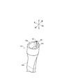
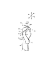
- the whole perspective view of the contact pin of a 1st embodiment of the present invention The perspective view which expands and shows the upper contact part of the contact pin of 1st Embodiment of this invention rather than FIG. 1A. Sectional drawing which shows the structure of the socket of the 1st Embodiment of this invention.
- the whole perspective view of the contact pin of a 2nd embodiment of the present invention The perspective view which expands and shows the upper contact part of the contact pin of 2nd Embodiment of this invention rather than FIG. 3A.
- the whole perspective view of the contact pin of the modification of the 2nd Embodiment of the present invention The perspective view which expands and shows the upper contact part of the contact pin of the modification of 2nd Embodiment of this invention from FIG. 4A.
- the whole perspective view of the contact pin of a 3rd embodiment of the present invention The perspective view which expands and shows the upper contact part of the contact pin of 3rd Embodiment of this invention from FIG. 5A.
- the whole perspective view of the contact pin of a 4th embodiment of the present invention The perspective view which expands and shows the upper contact part of the contact pin of 4th Embodiment of this invention from FIG. 6A.
- the contact pin will be described assuming that the first contact portion is arranged on the upper side, the second contact portion is arranged on the lower side, and the thickness direction is arranged in the front-rear direction.
- the arrangement of the contact pin and the socket is not limited to such arrangement.
- the direction in which the spring part (curved spring part) expands is the front, and the opposite direction is the rear, and the left and right are determined based on the front.
- FIGS. 1A and 1B are views showing a configuration of a contact pin
- FIG. 1A is an overall perspective view of the contact pin
- FIG. 1B is a perspective view showing an upper contact portion 20c (first contact portion) in an enlarged manner as compared with FIG. 1A. It is a figure.
- the contact pin 20 shown in FIGS. 1A and 1B is formed by pressing a metal plate material having excellent conductivity.
- the contact pin 20 extends in the vertical direction (first direction), and has a press-fitting portion 20a, a lower contact portion 20b (second contact portion), an upper contact portion 20c, and a bending spring portion 20d (spring portion). , And a straight portion 20e.
- the press-fitting portion 20a is formed in a linear shape.
- the lower contact portion 20b extends from the lower end of the press-fitting portion 20a and has a tapered shape.
- the upper contact portion 20c is located at the top of the contact pin 20.
- the bending spring portion 20d is located between the upper contact portion 20c and the press-fitting portion 20a and bends in an arc shape.
- the straight portion 20e extends upward from the upper end of the curved spring portion 20d and is connected to the upper contact portion 20c.
- the cross-sectional shape of the press-fitting portion 20a is substantially U-shaped, and a pair of slightly wider stopper pieces 20f are formed on the top of the press-fitting portion 20a.
- the curved spring portion 20d is formed by bending a portion of the contact pin 20 near the upper portion so as to obtain a predetermined elastic force.
- a pressing force is applied to the contact pin 20 in the axial direction (vertical direction in the present embodiment)
- the bending spring portion 20d elastically deforms to a state in which the bending radius becomes smaller, thereby shortening the total length of the contact pin 20 and at the same time.
- a reaction force that tends to extend the contact pin 20 upward is generated.
- the contact pin 20 has a width in a horizontal direction (a second direction intersecting with the first direction, hereinafter referred to as a “width direction”), and a first segment 20g is provided on one of the uppermost width directions thereof.
- the second segment 20h is provided on the other side.
- the first segment 20g and the second segment 20h are each curved so that their tips are close to each other, specifically, a substantially semi-cylindrical shape.
- the first segment 20g and the second segment 20h form a substantially cylindrical upper contact portion 20c.
- a tapered contact 20i is provided on the upper end of the tip of the first piece 20g.
- a tapered contact 20j is projectingly provided at the upper end of the tip of the second segment 20h.
- the first segment 20g and the second segment 20h are formed thinner than the other parts of the contact pin 20 and are configured to be vertically displaceable.
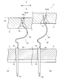
- FIG. 2 is a sectional view showing the structure of the socket.
- FIG. 2 for convenience, two different states of the socket are shown side by side. Note that, in FIG. 2, the IC package 100 and the wiring board 200 are indicated by a chain line for convenience.
- the socket 1 shown in FIG. 2 is intended to electrically connect the pad 100a, which is a terminal of the IC package 100, and the wiring board 200 in order to perform a performance test of the IC package 100.
- the terminals of the IC package 100 may be solder balls.
- the socket 1 includes a floating plate 10, a base member 15 (support), and a contact pin 20.
- a plurality of pads 100a which are terminals, are arranged in a matrix on the bottom surface of the IC package 100 connected to the socket 1.
- a plurality of contact pins 20 are arranged in a matrix so as to match the arrangement of the pads 100a.
- the floating plate 10 is provided above the base member 15 so as to be separable from and in contact with the base member 15.
- the floating plate 10 is biased upward by a coil spring (not shown).
- the floating plate 10 is provided with a plurality of through holes 10 a that penetrate the floating plate 10 in the vertical direction.
- the contact pins 20 are inserted into the respective through holes 10a, and the arrangement of the respective through holes 10a is the same as the arrangement of the contact pins 20 and the arrangement of the pads 100a of the IC package 100.
- the cut surface of each through hole 10a by the horizontal plane has a circular shape.
- each through-hole 10a has a columnar portion in the upper portion and a truncated cone portion in which the diameter increases as it goes downward.
- the base member 15 is provided with a plurality of through holes 15a penetrating the base member 15 in the vertical direction.
- the contact pins 20 are inserted into the respective through holes 15a, and the arrangement of the respective through holes 15a is the same as the arrangement of the contact pins 20, that is, the arrangement of the pads 100a and the arrangement of the through holes 10a.
- the cut surface of the through hole 15a by the horizontal surface has a circular shape.
- Each of the contact pins 20 is inserted into the through hole 10a and the through hole 15a which are arranged in the vertical direction. Specifically, the press-fitting portion 20a of each contact pin 20 is press-fitted into the through hole 15a of the base member 15 from above until the lower surface of the stopper piece 20f contacts the upper surface of the base member 15. Then, as shown in FIG. 2, the lower contact portion 20 b projects below the bottom surface of the base member 15. The lower contact portion 20b is inserted into a through hole (not shown) serving as a contact provided in the wiring board 200, soldered from the lower surface side of the wiring board 200, and electrically connected to the contact of the wiring board 200. It
- the socket 1 is arranged on the wiring board 200 in advance, and the lower contact portion 20b of the contact pin 20 is inserted into the wiring board 200. Then, the lower contact portion 20b is soldered to the through hole serving as the contact point of the wiring board 200. As a result, the socket 1 is in the state shown on the right side of FIG.
- the IC package 100 is set on the upper surface of the floating plate 10 and the IC package 100 is pressed downward. As a result, the floating plate 10 is pushed down against the biasing force of the coil spring.
- first segment 20g and the second segment 20h can be vertically displaced. Therefore, even if there is a difference between the height of the contact 20i of the first piece 20g and the height of the contact 20j of the second piece 20h due to manufacturing error, wear, or the like, the contact 20i and the contact 20j are separated when the IC package 100 presses. Since the displacement is downward, the difference can be absorbed by the displacement. Further, at that time, a stronger reaction force is generated on the higher contact of the contacts 20i and 20j, and this contact presses the pad 100a of the IC package 100 more strongly.
- a plurality of contacts simultaneously contact the pad 100a of the IC package 100 and the contact between the contact pin 20 and the pad 100a becomes stable.
- the conductivity of the contact pin can be improved more than before, and the contact pin 20 and the socket 1 can handle high current.
- first segment 20g and the second segment 20h are relatively simple shapes curved in an arc shape, the upper contact portion 20c and thus the contact pin 20 can be easily manufactured.
- FIGS. 3A and 3B are views showing the structure of the contact pin
- FIG. 3A is an overall perspective view of the contact pin
- FIG. 3B is a perspective view showing the upper contact portion 30a (first contact portion) in an enlarged manner compared to FIG. 3A. It is a figure.
- the contact pin 30 has a configuration in which the upper contact portion 20c of the contact pin 20 (see FIG. 1) of the first embodiment is replaced with an upper contact portion 30a. Further, the contact pin 30 is obtained by replacing the press-fitting portion 20a of the contact pin 20 according to the first embodiment with a press-fitting portion 25a having a smaller lower dimension in the front-rear direction than the press-fitting portion 20a.
- the upper contact portion 30a includes a first piece 30b, a second piece 30c, and a base piece 30d.
- the first segment 30b is continuously provided on the uppermost left end surface of the linear portion 20e
- the second segment 30c is continuously provided on the uppermost right end surface of the linear portion 20e.
- the base piece 30d extends upward from the uppermost portion of the linear portion 20e and has a shape like an isosceles triangle joined to the upper portion of a circle.
- the first segment 30b, the second segment 30c, and the base piece 30d are all formed thinner than the other parts of the contact pin 30, and are configured to be displaceable upward and downward respectively.
- first segment 30b and the second segment 30c are symmetrical in the front-rear direction and in the left-right direction, the configuration will be described in detail by taking the second segment 30c as an example.
- the second segment 30c includes a first portion 30cb on the base portion 30ca side and a second portion 30cd on the tip end side.
- the second piece 30c is bent backward (toward the rear surface of the base piece 30d) at the base portion 30ca, and the first portion 30cb is overlapped with the rear surface of the base piece 30d.
- the second section 30c is bent rearward at an intermediate portion 30cc, and the second portion 30cd faces the rear surface of the base piece 30d vertically (or substantially vertically).
- the second portion 30cd has a substantially arc-shaped curved portion R1 in which the front end surface and the rear end surface bulge rearward, and the intermediate portion 30cc described above is located closer to the base end side than the curved portion R1.
- the tip of the second portion 30cd is in contact with the front surface of the base piece 30d at a position where the upper end 30ce thereof is slightly lower than the upper end 30da of the base piece 30d.
- the upper end 30ce of the second piece 30c (and the upper end 30be of the first piece 30b) is arranged slightly below the upper end 30da of the base piece 30d.
- the second portion 30cd of the second piece 30c (and the second portion 30bd of the first piece 30b) extends in the vertical direction when viewed from the front or the rear. That is, each of the second portions 30bd and 30cd is in a posture along the axial direction of the contact pin 30.
- the upper end 30ce, the upper end 30be, and the upper end 30da function as contacts that come into contact with the pad 100a of the IC package 100. Therefore, the upper end 30ce, the upper end 30be, and the upper end 30da are hereinafter referred to as a contact point 30ce, a contact point 30be, and a contact point 30da.
- the first segment 30b and the second segment 30c are formed into such a bent shape so that the contact point 30ce and the contact point 30be at the tip are arranged close to each other.
- the other configuration of the contact pin 30 is the same as that of the contact pin 20 of the first embodiment, and the description thereof will be omitted. Further, the structure of the socket is the same as that of the socket 1 of the first embodiment except that the contact pin 30 is used, and therefore the description thereof will be omitted.
- the first segment 30b, the second segment 30c, and the base piece 30d are each vertically displaceable. Therefore, when the pad 100a of the IC package 100 is pressed, first, the contact 30da of the base piece 30d is pressed by the pad 100a and elastically deforms and curves. Then, the contact point 30be of the first piece 30b and the contact point 30ce of the second piece 30c are pressed. When the heights of the contacts 30be and 30ce are different due to manufacturing error, one of the contacts 30be and 30ce is pressed by the pad 100a.
- the contact pin 30 and the socket 1 can handle high current.
- FIGS. 4A and 4B are views showing the configuration of the contact pin
- FIG. 4A is an overall perspective view of the contact pin
- FIG. 4B is a perspective view showing the upper contact portion 35a (first contact portion) in an enlarged manner compared to FIG. 4A. It is a figure.
- the contact pin 35 shown in FIGS. 4A and 4B has a configuration in which the upper contact portion 30a of the contact pin 30 shown in FIGS. 3A and 3B is replaced with an upper contact portion 35a. 35c is different from the first segment 30b and the second segment 30c.
- the second segment 35c Since the first segment 35b and the second segment 35c are symmetrical to each other in the front-rear direction and the left-right direction, the second segment 35c will be mainly used as an example to describe the configuration in detail.
- the second segment 35c includes a first portion 35cb on the base 35ca side and a second portion 35cd on the tip side.
- the second segment 35c is bent rearward (toward the rear surface of the base piece 30d) by about 45 degrees at the base portion 35ca, and the first portion 35cb faces the rear surface of the base piece 30d with a space therebetween.
- the second portion 35cd is bent at an angle of about 45 degrees in the intermediate portion 35cc so that the tip end thereof faces the rear surface of the base piece 30d vertically (or substantially vertically).
- the second portion 35 cd has a substantially arc-shaped curved portion R2 in which the front end surface and the rear end surface bulge rearward.
- the intermediate portion 35cc described above is located closer to the tip side than the curved portion R2.
- the tip of the second portion 35cd is located on the right side and below the contact 30da, and the contact 35ce is provided on the upper surface thereof so as to project.
- the contact point 35ce has a rectangular shape that is long in the front-rear direction when viewed from above.
- the first segment 35b is bent forward by the base portion 35ba (toward the front surface of the base piece 30d) by about 45 degrees.
- the second portion 35bd on the tip side of the first segment 35b is bent at an intermediate portion by about 45 degrees so that its tip faces vertically (or substantially vertically) to the front surface of the base piece 30d.
- the second portion 35bd has a substantially arc shape in which the front end face and the rear end face are curved so as to bulge forward.
- the above-mentioned middle part is located in the tip side rather than this curved part.
- the second portion 35bd is located on the left side and the lower side of the contact point 30da, and the contact point 35be is projectingly provided on the upper surface thereof.
- the contact 35be has a rectangular shape that is long in the front-rear direction when viewed from above.
- the other configurations are similar to those of the contact pin 30 shown in FIGS. 3A and 3B, and the description thereof will be omitted. Further, the structure of the socket is the same as that of the socket 1 of the first embodiment except that the contact pin 35 is used, and therefore the description thereof is omitted.
- FIGS. 5A and 5B are views showing the configuration of the contact pin
- FIG. 5A is an overall perspective view of the contact pin
- FIG. 5B is a perspective view showing the upper contact portion 40a (first contact portion) in an enlarged manner compared to FIG. 5A. It is a figure.
- the upper contact portion 30a of the contact pin 30 of the second embodiment is replaced by the upper contact portion 40a (first Contact part).
- the base piece 40d has a cutout portion 40da that is recessed downward instead of the contact point 30da on the upper side of the base piece 30d of the second embodiment.
- the notch 40da has a left side surface, a bottom surface, and a right side surface.
- the lower surface of the tip of the first segment 30b (the portion directly below the contact point 30be) and the lower surface of the tip of the second segment 30c (the portion directly below the contact point 30ce) are placed on the bottom surface of the cutout portion 40da, or the bottom surface. Is arranged above the bottom surface with a slight gap.
- the contact point 30be of the first piece 30b and the contact point 30ce of the second piece 30c are arranged side by side in the width direction.
- the tip of the first piece 30b is designed not to exceed the rear surface of the base piece 40d, but the tip may be arranged to exceed the rear surface of the base piece 40d.
- the first segment 30b may cross over the notch 40da from the front.
- the second segment 30c may be mounted over the notch 40da later.
- the other configurations are similar to those of the contact pin 30 of the second embodiment, and the description thereof will be omitted. Further, the structure of the socket is the same as that of the socket 1 of the first embodiment except that the contact pin 40 is used, and therefore the description thereof is omitted.
- the bottom surface of the cutout 40da functions as a stopper that restricts excessive downward displacement of the first segment 30b and the second segment 30c. Therefore, when the contacts 30be and 30ce of the contact pin 40 are pressed by the IC package, it is possible to prevent the first segment 30b and the second segment 30c from being damaged by being plastically deformed due to excessive displacement.
- FIGS. 6A and 6B are views showing the configuration of the contact pin
- FIG. 6A is an overall perspective view of the contact pin
- FIG. 6B is a perspective view showing the upper contact portion 50a (first contact portion) in an enlarged manner compared to FIG. 6A. It is a figure.
- the contact pin 50 includes a first segment 50b and a second segment 50c in which the upper contact portions 50a are arranged side by side in the width direction.
- the first segment 50b has a shape in which the front end portion on the center side (right side) in the width direction of the contact pin 50 is sharpened upward, and the apex thereof contacts the pad 100a (see FIG. 2) of the IC package 100.
- the second section 50c has a shape in which the widthwise center side (left side) and rear end of the contact pin 50 is sharpened upward, and this apex functions as a contact point 50e in contact with the pad 100a.
- the first segment 50b is bent slightly forward with respect to the straight part 20e, and conversely, the second segment 50c is slightly bent backward with respect to the straight part 20e.
- the contacts 50d and 50e are arranged with their positions shifted forward and backward.
- the first piece 50b has a shallow bowl-like shape (curved shape) in which both the front surface and the rear surface bulge forward.
- the second piece 50c has a shallow bowl-like shape (curved shape) in which the front surface and the rear surface both bulge rearward.
- first segment 50b and the second segment 50c are formed thinner than other parts of the contact pin 50 so that they can be easily displaced.
- the other configurations are similar to those of the contact pin 30 of the second embodiment, and the description thereof will be omitted. Further, the structure of the socket is the same as that of the socket 1 of the first embodiment except that the contact pin 50 is used, and therefore the description thereof is omitted.
- the same effect as that of the first embodiment is obtained, and further, the first segment 50b and the second segment 50c are curved so as to bulge in mutually opposite directions. Therefore, the pad 100a can be received with good balance.
- the contact pin and socket of the present invention are applied for inspection of IC packages, but the contact pin and socket of the present invention are not limited to this, and for inspection of other electric parts. Alternatively, it can be applied to various other uses.
- the present invention is preferably used as contact pins and sockets.
Landscapes
- Physics & Mathematics (AREA)
- Engineering & Computer Science (AREA)
- General Physics & Mathematics (AREA)
- Computer Hardware Design (AREA)
- Microelectronics & Electronic Packaging (AREA)
- General Engineering & Computer Science (AREA)
- Environmental & Geological Engineering (AREA)
- Geometry (AREA)
- Measuring Leads Or Probes (AREA)
- Testing Of Individual Semiconductor Devices (AREA)
- Connecting Device With Holders (AREA)
Abstract
コンタクトピンは、第1方向の一端側に設けられた第1接触部と、前記第1方向の他端側に設けられた第2接触部と、前記第1接触部と前記第2接触部との間の中間部に設けられ、弾性変形可能なばね部とを備え、前記第1接触部と前記第2接触部と前記中間部とは一体に形成され、前記第1接触部は、前記第1方向にそれぞれ変位可能な切片を複数備える。
Description
本発明は、コンタクトピン及びソケットに関する。
例えば特許文献1に記載されているように、従来、ICパッケージ等の電気部品を検査する際、ソケットが用いられている。このソケットは、電気部品と検査装置側の基板である検査用基板とを電気的に接続する複数のコンタクトピンを備えている。
これらのコンタクトピンは、その上端部に、電気部品の端子に接触する第1接触部を有し、その中間部に湾曲ばね部を有し、その下端部に、検査用基板の端子に接触する第2接触部を有する。
このようなコンタクトピンでは、高電流を流すことができるように導電性の向上が要望されている。
本発明は、このような要望に鑑み創案されたものであり、導電性を向上させて高電流に対応できるようにすることを目的とする。
上記従来の課題を解決するために、本発明のコンタクトピンは、第1方向の一端側に設けられた第1接触部と、前記第1方向の他端側に設けられた第2接触部と、前記第1接触部と前記第2接触部との間の中間部に設けられ、弾性変形可能なばね部とを備え、前記第1接触部と前記第2接触部と前記中間部とは一体に形成され、前記第1接触部は、前記第1方向にそれぞれ変位可能な切片を複数備える。
上記従来の課題を解決するために、本発明のソケットは、コンタクトピンと、前記コンタクトピンが挿入される貫通孔を有する支持体と、を備える。
本発明によれば、導電性を向上させて高電流に対応できる。
以下、本発明の実施の形態に係るコンタクトピン及びソケットついて、図面を参照しながら説明する。以下に示す各実施の形態はあくまでも例示に過ぎず、以下の各実施の形態で明示しない種々の変形や技術の適用を排除するものではない。また、各実施の形態の各構成は、それらの趣旨を逸脱しない範囲で種々変形して実施することができる。さらに、各実施の形態の各構成は、必要に応じて取捨選択することができ、あるいは適宜組み合わせることができる。
なお、以下の各実施形態では、便宜的に、コンタクトピンは、第1接触部が上側に、第2接触部が下側に、厚み方向が前後方向に配置されているものとして説明を行う。但し、コンタクトピン及びソケットの配置がそのような配置に限られないことは言うまでもない。
また、ばね部(湾曲ばね部)が膨出する方向を前方、その反対を後方とし、前方を基準に左右を定める。
また、実施の形態を説明するための全図において、同一要素は原則として同一の符号を付し、その説明を省略することもある。
以下、本発明の実施の形態に係るコンタクトピン及びソケットについて図面を参照しながら詳細に説明する。
[1.第1実施形態]
[1-1.構成]
[1-1-1.コンタクトピンの構成]
本発明の第1実施形態のコンタクトピンの構成について、図1A及び図1Bを参照して説明する。図1A及び図1Bはコンタクトピンの構成を示す図であって、図1Aはコンタクトピンの全体斜視図、図1Bは上部接触部20c(第1接触部)を図1Aよりも拡大して示す斜視図である。
[1-1.構成]
[1-1-1.コンタクトピンの構成]
本発明の第1実施形態のコンタクトピンの構成について、図1A及び図1Bを参照して説明する。図1A及び図1Bはコンタクトピンの構成を示す図であって、図1Aはコンタクトピンの全体斜視図、図1Bは上部接触部20c(第1接触部)を図1Aよりも拡大して示す斜視図である。
図1A及び図1Bに示すコンタクトピン20は、導電性に優れた金属板材をプレス加工して形成される。このコンタクトピン20は、鉛直方向(第1方向)に延在し、圧入部20aと、下部接触部20b(第2接触部)と、上部接触部20cと、湾曲ばね部20d(ばね部)と、直線部20eとを有している。圧入部20aは直線状に形成される。下部接触部20bは、圧入部20aの下端から延在し、テーパ状に形成される。上部接触部20cは、コンタクトピン20の最上部に位置する。湾曲ばね部20dは、上部接触部20cと圧入部20aとの間に位置し、円弧状に湾曲する。直線部20eは、湾曲ばね部20dの上端から上方に延びて上部接触部20cに繋がる。
圧入部20aの横断面形状は、略Uの字形状であり、圧入部20aの上部にはやや幅広な一対のストッパ片20fが形成されている。
湾曲ばね部20dは、コンタクトピン20の上部寄りの部位を、所定の弾性力が得られるように湾曲させたものである。湾曲ばね部20dは、コンタクトピン20に軸方向(本実施形態では鉛直方向)への押圧力が加わった際に、湾曲半径が小さくなる状態に弾性変形し、コンタクトピン20の全長を短くすると同時に、コンタクトピン20を上方に伸ばそうとする反力を生じさせる。
コンタクトピン20は、水平方向(第1方向と交差する第2方向、以下「幅方向」という)に幅を有し、その最上部の幅方向の一方に第1切片20gが設けられ、幅方向の他方に第2切片20hが設けられる。第1切片20gと第2切片20hとは、それぞれ、先端が互いに近接するような湾曲形状、詳しくは略半円筒形状とされている。これらの第1切片20gと第2切片20hとにより略円筒状の上部接触部20cが構成される。また、第1切片20gの当該先端の上端には、テーパ状の接点20iが突設されている。同様に、第2切片20hの当該先端の上端には、テーパ状の接点20jが突設されている。
また、第1切片20g及び第2切片20hは、コンタクトピン20の他の部位よりも薄肉に形成されており、鉛直方向に変位可能に構成されている。
[1-1-2.ソケットの構成]
本発明の第1実施形態のソケットの構成について図2を参照して説明する。図2はソケットの構成を示す断面図である。図2では、便宜的に、ソケットの2つの異なる状態を横に並べて示している。なお、図2では便宜的にICパッケージ100及び配線基板200が一点鎖線で示されている。
本発明の第1実施形態のソケットの構成について図2を参照して説明する。図2はソケットの構成を示す断面図である。図2では、便宜的に、ソケットの2つの異なる状態を横に並べて示している。なお、図2では便宜的にICパッケージ100及び配線基板200が一点鎖線で示されている。
図2示すソケット1は、ICパッケージ100の性能試験を行うために、このICパッケージ100の端子であるパッド100aと、配線基板200との電気的接続を図るものである。なお、ICパッケージ100の端子は半田ボールであってもよい。
ソケット1は、フローティングプレート10と、ベース部材15(支持体)と、コンタクトピン20と、を備える。
ソケット1に接続されるICパッケージ100の底面には、端子であるパッド100aがマトリックス状に複数配置される。コンタクトピン20は、このパッド100aの配置に一致するようにマトリックス状に複数配置される。
フローティングプレート10は、ベース部材15の上方に、ベース部材15に対し離接可能に設けられている。フローティングプレート10は、図示しないコイルスプリングにより上方に付勢されている。
フローティングプレート10には、フローティングプレート10を鉛直方向に貫通する貫通孔10aが複数設けられている。各貫通孔10aにはコンタクトピン20が挿通され、各貫通孔10aの配置は、コンタクトピン20の配置ひいてはICパッケージ100のパッド100aの配置と一致している。また、各貫通孔10aの水平面による切断面は円形を呈する。詳しくは、各貫通孔10aは、上部に円柱形状部を備え、下部に、下方になるほど径が大きくなる円錐台形状部を備える。
同様に、ベース部材15には、ベース部材15を鉛直方向に貫通する貫通孔15aが複数設けられる。各貫通孔15aにはコンタクトピン20が挿通され、これらの各貫通孔15aの配置は、コンタクトピン20の配置ひいてはパッド100aの配置及び貫通孔10aの配置と一致している。また、貫通孔15aの水平面による切断面は円形を呈する。
各コンタクトピン20は、鉛直方向に並ぶ貫通孔10aと貫通孔15aとに挿通されている。詳しくは、各コンタクトピン20の圧入部20aは、ストッパ片20fの下面がベース部材15の上面に当接するまでベース部材15の貫通孔15aに上方から圧入される。すると、図2に示すように、下部接触部20bがベース部材15の底面よりも下方に突出する。この下部接触部20bが、配線基板200に設けられた接点となる貫通孔(非図示)に挿通されて、配線基板200の下面側からハンダ付けされ、配線基板200の接点に電気的に導通される。
ソケット1の使用方法の概略について説明すると、予め、配線基板200上にソケット1を配設し、コンタクトピン20の下側接触部20bを配線基板200に挿通する。そして、下側接触部20bを、配線基板200の接点となる貫通孔に半田付けしておく。これにより、ソケット1は、図2の右側に示す状態となる。
次いで、ICパッケージ100をフローティングプレート10の上面にセットし、ICパッケージ100を下方に押圧する。その結果、フローティングプレート10がコイルスプリングの付勢力に抗して下方に押し下げられる。
これにより、図2の左側に示す状態となる。具体的には、上側接触部20cに近接して配置された接点20i,20jが、ICパッケージ100の同じパッド100aに同時に当接する。そして、フローティングプレート10が更に押し下げられると、湾曲ばね部20dが弾性変形して、湾曲ばね部20dに付勢力が発生するようになる。この結果、上側接触部20cの接点20i,20jが、ICパッケージ100のパッド100aに所定の接圧で押圧されるようになる。
この状態で、ICパッケージ100に電流を流してバーンイン試験等が行われる。
[1-1-3.作用効果]
本発明の第1実施形態によれば次のような作用効果が得られる。
本発明の第1実施形態によれば次のような作用効果が得られる。
(1)コンタクトピン20では、ICパッケージ100による押圧時に、第1切片20gの接点20iと、第2切片20hの接点20jとの2つの接点が同時にICパッケージ100の同じパッド100aに接触するようになる。
さらに、第1切片20gと第2切片20hとが上下に変位可能となっている。よって、第1切片20gの接点20iの高さと、第2切片20hの接点20jの高さとに製作誤差または摩耗等により差がある場合でも、ICパッケージ100による押圧時に接点20iと接点20jとが個別に下方に変位するので、この差を当該変位により吸収できる。さらに、その際、接点20i,20jの内、高いほうの接点には、より強い反力が生じ、この接点が、ICパッケージ100のパッド100aに、より強く押圧する。
したがって、複数の接点(本実施形態では2つ接点20i,20j)がICパッケージ100のパッド100aに同時に接触すると共にコンタクトピン20とパッド100aとの接触が安定するようになる。この結果、コンタクトピンの導電性を従来よりも向上させることができ、コンタクトピン20及びソケット1が高電流に対応できるようになる。
また、第1切片20gと第2切片20hとは円弧状に湾曲させた比較的に単純な形状なので、上部接触部20cひいてはコンタクトピン20を容易に製造できる。
[2.第2実施形態]
[2-1.構成]
本発明の第2実施形態のコンタクトピンの構成について、図3A及び図3Bを参照して説明する。図3A及び図3Bはコンタクトピンの構成を示す図であって、図3Aはコンタクトピンの全体斜視図、図3Bは上部接触部30a(第1接触部)を図3Aよりも拡大して示す斜視図である。
[2-1.構成]
本発明の第2実施形態のコンタクトピンの構成について、図3A及び図3Bを参照して説明する。図3A及び図3Bはコンタクトピンの構成を示す図であって、図3Aはコンタクトピンの全体斜視図、図3Bは上部接触部30a(第1接触部)を図3Aよりも拡大して示す斜視図である。
図3A及び図3Bに示すように、コンタクトピン30は、第1実施形態のコンタクトピン20(図1参照)の上部接触部20cを、上部接触部30aに置き換えた構成のものである。また、コンタクトピン30は、第1実施形態のコンタクトピン20の圧入部20aを、圧入部20aに比べて下部の前後方向の寸法が小さな圧入部25aに置き換えたものである。
図3Bに示すように、上部接触部30aは、第1切片30bと、第2切片30cと、ベース片30dとを備える。第1切片30bは、直線部20eの最上部の左端面に連設され、第2切片30cは、直線部20eの最上部の右端面に連設される。ベース片30dは、直線部20eの最上部から上方に延設され、円の上部に二等辺三角形を接合したような形状とされている。第1切片30bと、第2切片30cと、ベース片30dとは、何れもコンタクトピン30の他の部位よりも薄肉に形成されており、上方及び下方のそれぞれに変位可能に構成されている。
第1切片30bと第2切片30cとは前後に且つ左右に対称なので、第2切片30cを例に取りその構成を詳しく説明する。
第2切片30cは、基部30ca側の第1部位30cbと、先端側の第2部位30cdとを備える。第2切片30cは、基部30caで後方に(ベース片30dの後面に向けて)折り曲げられており、第1部位30cbはベース片30dの後面に重合されている。第2切片30cは、その中間部30ccで後方に折り曲げられており、第2部位30cdはベース片30dの後面に対して垂直(又は略垂直)に対向している。
第2部位30cdは、前端面及び後端面が後方に膨らむ略円弧形状の湾曲部R1を有し、前述の中間部30ccは湾曲部R1よりも基端側に位置する。第2部位30cdの先端は、その上端30ceがベース片30dの上端30daよりも僅かに低くなる位置でベース片30dの前面に当接している。換言すれば、第2切片30cの上端30ce(及び第1切片30bの上端30be)は、ベース片30dの上端30daよりも僅かに下方に配置される。また、第2切片30cの第2部位30cd(及び第1切片30bの第2部位30bd)は、前方又は後方から視た場合に鉛直方向に延在する。すなわち、第2部位30bd,30cdはそれぞれコンタクトピン30の軸方向に沿った姿勢とされる。
上端30ce,上端30be及び上端30daは、ICパッケージ100のパッド100aに接触する接点として機能する。よって、これらの上端30ce,上端30be及び上端30daを、以降、接点30ce,接点30be及び接点30daと称する。
第1切片30bと第2切片30cとをこのような折り曲げ形状とすることで、先端の接点30ceと接点30beとが近接して配置されるようにしている。
コンタクトピン30のこの他の構成は、第1実施形態のコンタクトピン20と同様なので説明を省略する。また、ソケットの構成は、コンタクトピン30を使用する以外は第1実施形態のソケット1と同様なので説明を省略する。
[2-2.作用効果]
本発明の第1実施形態によれば次のような作用効果が得られる。
本発明の第1実施形態によれば次のような作用効果が得られる。
第1切片30b,第2切片30c及びベース片30dがそれぞれ鉛直方向に変位可能となっている。よって、ICパッケージ100のパッド100aによる押圧時には、先ず、ベース片30dの接点30daがパッド100aに押圧されて弾性変形して湾曲する。その後、第1切片30bの接点30be及び第2切片30cの接点30ceが押圧される。接点30be,30ceの高さが製造誤差により相異する場合には接点30be,30ceの一方が、パッド100aに押圧される。
よって、少なくとも2つの接点が同時にパッド100aに接触するようになるので、本発明の第2実施形態によれば、第1実施形態と同様に、従来よりもコンタクトピンの導電性を向上させることができ、コンタクトピン30及びソケット1が高電流に対応できるようになる。
[2-3.変形例]
本発明の第2実施形態のコンタクトピンの変形例の構成について、図4A及び図4Bを参照して説明する。図4A及び図4Bはコンタクトピンの構成を示す図であって、図4Aはコンタクトピンの全体斜視図、図4Bは上部接触部35a(第1接触部)を図4Aよりも拡大して示す斜視図である。
本発明の第2実施形態のコンタクトピンの変形例の構成について、図4A及び図4Bを参照して説明する。図4A及び図4Bはコンタクトピンの構成を示す図であって、図4Aはコンタクトピンの全体斜視図、図4Bは上部接触部35a(第1接触部)を図4Aよりも拡大して示す斜視図である。
図4A及び図4Bに示すコンタクトピン35は、図3A及び図3Bに示すコンタクトピン30の上部接触部30aを、上部接触部35aに置き換えた構成のものであり、第1切片35b及び第2切片35cが、第1切片30b及び第2切片30cと異なる。
第1切片35bと第2切片35cとは前後に且つ左右に対称なので、第2切片35cを主に例に取り、その構成を詳しく説明する。
第2切片35cは、基部35ca側の第1部位35cbと、先端側の第2部位35cdとを備える。第2切片35cは、基部35caで後方に(ベース片30dの後面に向けて)45度程度だけ折り曲げられており、第1部位35cbはベース片30dの後面に間隔を空けて対面している。第2部位35cdはその先端がベース片30dの後面に対して垂直(又は略垂直)に対向するように、中間部35ccにおいて45度程度だけ折り曲げられている。
第2部位35cdは前端面及び後端面が後方に膨らむ略円弧形状の湾曲部R2を有する。上述の中間部35ccは、この湾曲部R2よりも先端側に位置している。第2部位35cdの先端は、接点30daよりも右側且つ下側に位置し、その上面には接点35ceが突設されている。この接点35ceは、上方から視て前後に長い矩形の形状とされている。
第1切片35bは、基部35baで前方に(ベース片30dの前面に向けて)45度程度だけ折り曲げられている。第1切片35bの先端側の第2部位35bdは、その先端がベース片30dの前面に対して垂直(又は略垂直)に対向するように、中間部において、45度程度だけ折り曲げられている。第2部位35bdは前端面及び後端面が前方に膨らむように湾曲した略円弧形状とされている。上述の中間部は、この湾曲部よりも先端側に位置している。第2部位35bdは、接点30daよりも左側且つ下側に位置し、その上面には接点35beが突設されている。この接点35beは、上方から視て前後に長い矩形の形状とされている。
この他の構成は、図3A及び図3Bに示すコンタクトピン30と同様なので説明を省略する。また、ソケットの構成は、コンタクトピン35を使用する以外は第1実施形態のソケット1と同様なので説明を省略する。
[3.第3実施形態]
[3-1.構成]
本発明の第3実施形態のコンタクトピンの構成について、図5A及び図5Bを参照して説明する。図5A及び図5Bはコンタクトピンの構成を示す図であって、図5Aはコンタクトピンの全体斜視図、図5Bは上部接触部40a(第1接触部)を図5Aよりも拡大して示す斜視図である。
[3-1.構成]
本発明の第3実施形態のコンタクトピンの構成について、図5A及び図5Bを参照して説明する。図5A及び図5Bはコンタクトピンの構成を示す図であって、図5Aはコンタクトピンの全体斜視図、図5Bは上部接触部40a(第1接触部)を図5Aよりも拡大して示す斜視図である。
図5A及び図5Bに示す本発明の第3実施形態のコンタクトピン40は、第2実施形態のコンタクトピン30(図3A及び図3B参照)の上部接触部30aを、上部接触部40a(第1接触部)に置き換えた構成のものである。
具体的には、ベース片40dは、第2実施形態のベース片30dに対し、上部に、接点30daに替えて下方に凹設された切欠き部40daを有する。切欠き部40daは、左側面,底面及び右側面を有している。第1切片30bの先端下面(接点30beの真下の部位)と、第2切片30cの先端下面(接点30ceの真下の部位)とは、切欠き部40daの底面に載置され、或いは、当該底面から僅かに隙間を空けて当該底面の上方に配置されている。また、第1切片30bの接点30beと、第2切片30cの接点30ceとは、幅方向並んで配置される。
なお、本実施形態では、第1切片30bは、その先端がベース片40dの後面を超えないようにされているが、当該先端がベース片40dの後面を超えるようにしてもよい。換言すれば、第1切片30bは、前から切欠き部40daを乗り越えるようにしてもよい。同様に、第2切片30cは、後から切欠き部40daを乗り越えるようにしてもよい。
この他の構成は、第2実施形態のコンタクトピン30と同様なので説明を省略する。また、ソケットの構成は、コンタクトピン40を使用する以外は第1実施形態のソケット1と同様なので説明を省略する。
[3-2.作用効果]
本発明の第3実施形態によれば、第2実施形態の効果に加えて次のような作用効果が得られる。つまり、切欠き部40daの底面が、第1切片30b及び第2切片30cの下方への過剰な変位を規制するストッパとして機能する。したがって、ICパッケージによってコンタクトピン40の接点30be,30ceが押圧された際に、第1切片30b及び第2切片30cが、過剰な変位により塑性変形するなど損傷することを抑制できる。
本発明の第3実施形態によれば、第2実施形態の効果に加えて次のような作用効果が得られる。つまり、切欠き部40daの底面が、第1切片30b及び第2切片30cの下方への過剰な変位を規制するストッパとして機能する。したがって、ICパッケージによってコンタクトピン40の接点30be,30ceが押圧された際に、第1切片30b及び第2切片30cが、過剰な変位により塑性変形するなど損傷することを抑制できる。
[4.第4実施形態]
[4-1.構成]
本発明の第4実施形態のコンタクトピンの構成について、図6A及び図6Bを参照して説明する。図6A及び図6Bはコンタクトピンの構成を示す図であって、図6Aはコンタクトピンの全体斜視図、図6Bは上部接触部50a(第1接触部)を図6Aよりも拡大して示す斜視図である。
[4-1.構成]
本発明の第4実施形態のコンタクトピンの構成について、図6A及び図6Bを参照して説明する。図6A及び図6Bはコンタクトピンの構成を示す図であって、図6Aはコンタクトピンの全体斜視図、図6Bは上部接触部50a(第1接触部)を図6Aよりも拡大して示す斜視図である。
図6A及び図6Bに示すように、コンタクトピン50は、上部接触部50aが、幅方向に並べて設けられた第1切片50b及び第2切片50cを備える。第1切片50bは、コンタクトピン50の幅方向中心側(右側)且つ前方の端部が上方に尖った形状とされ、この頂点がICパッケージ100のパッド100a(図2参照)と接触する接点50dとして機能する。また、第2切片50cは、コンタクトピン50の幅方向中心側(左側)且つ後方の端部が上方に尖った形状とされ、この頂点がパッド100aと接触する接点50eとして機能する。
第1切片50bは直線部20eに対し僅かに前方に折り曲げられ、逆に第2切片50cは直線部20eに対し僅かに後方に折り曲げられている。これにより接点50d,50eが前後に位置をずらして配置される。さらに、第1切片50bは、前面及び後面が共に前方に膨出した浅いお椀のような形状(湾曲形状)とされている。第2切片50cは、反対に、前面及び後面が共に後方に膨出した浅いお椀のような形状(湾曲形状)とされている。
また、第1切片50b及び第2切片50cは、変位しやすいように、コンタクトピン50の他の部位よりも薄肉に形成されている。
この他の構成は、第2実施形態のコンタクトピン30と同様なので説明を省略する。また、ソケットの構成は、コンタクトピン50を使用する以外は第1実施形態のソケット1と同様なので説明を省略する。
[4-2.作用効果]
コンタクトピン50が上述したように構成されているので、パッド100aによる押圧時、第1切片50bは前方に膨らむように湾曲し、逆に第2切片50cは後方に膨らむように湾曲し、第1切片50bと第2切片50cとが個別に鉛直方向に変位する。
コンタクトピン50が上述したように構成されているので、パッド100aによる押圧時、第1切片50bは前方に膨らむように湾曲し、逆に第2切片50cは後方に膨らむように湾曲し、第1切片50bと第2切片50cとが個別に鉛直方向に変位する。
したがって、本発明の第4実施形態の発明によれば、第1実施形態と同様の効果が得られる他、第1切片50b及び第2切片50cが互いに逆方向に膨出するように湾曲するので、バランスよくパッド100aを受け止めることができる。
[5.その他]
前記の各実施形態では、本発明のコンタクトピン及びソケットを、ICパッケージの検査用に適用したが、本発明のコンタクトピン及ソケットは、これに限られるものではなく、他の電気部品の検査用又はその他の種々の用途に適用できる。
前記の各実施形態では、本発明のコンタクトピン及びソケットを、ICパッケージの検査用に適用したが、本発明のコンタクトピン及ソケットは、これに限られるものではなく、他の電気部品の検査用又はその他の種々の用途に適用できる。
本出願は、2018年10月29日出願の特願2018-203016に基づく優先権を主張する。これらの出願明細書および図面に記載された内容は、すべて本願明細書に援用される。
本発明は、コンタクトピン及びソケットとして好適に利用される。
1 ソケット
10 フローティングプレート
10a 貫通孔
15 ベース部材(支持体)
15a 貫通孔
20,30,35,40,50 コンタクトピン
20a,25a 圧入部
20b 下部接触部(第2接触部)
20c 上部接触部(第1接触部)
20d 湾曲ばね部(ばね部)
20e 直線部
20f ストッパ片
20g 第1切片
20h 第2切片
20i 接点
20j 接点
30a 上部接触部(第1接触部)
30b 第1切片
30bd 第2部位
30be 接点
30c 第2切片
30ca 基部
30cb 第1部位
30cc 中間部
30cd 第2部位
30ce 接点
30d ベース片
30da 上端
35a 上部接触部(第1接触部)
35b 第1切片
35ba 基部
35bd 第2部位
35be 接点
35c 第2切片
35ca 基部
35cb 第1部位
35cc 中間部
35cd 第2部位
35ce 接点
40d ベース片
40da 切欠き部
50a 上部接触部(第1接触部)
50b 第1切片
50c 第2切片
50d,50e 接点
100 ICパッケージ
100a パッド
200 配線基板
R1,R2 湾曲部
10 フローティングプレート
10a 貫通孔
15 ベース部材(支持体)
15a 貫通孔
20,30,35,40,50 コンタクトピン
20a,25a 圧入部
20b 下部接触部(第2接触部)
20c 上部接触部(第1接触部)
20d 湾曲ばね部(ばね部)
20e 直線部
20f ストッパ片
20g 第1切片
20h 第2切片
20i 接点
20j 接点
30a 上部接触部(第1接触部)
30b 第1切片
30bd 第2部位
30be 接点
30c 第2切片
30ca 基部
30cb 第1部位
30cc 中間部
30cd 第2部位
30ce 接点
30d ベース片
30da 上端
35a 上部接触部(第1接触部)
35b 第1切片
35ba 基部
35bd 第2部位
35be 接点
35c 第2切片
35ca 基部
35cb 第1部位
35cc 中間部
35cd 第2部位
35ce 接点
40d ベース片
40da 切欠き部
50a 上部接触部(第1接触部)
50b 第1切片
50c 第2切片
50d,50e 接点
100 ICパッケージ
100a パッド
200 配線基板
R1,R2 湾曲部
Claims (8)
- 第1方向の一端側に設けられた第1接触部と、
前記第1方向の他端側に設けられた第2接触部と、
前記第1接触部と前記第2接触部との間の中間部に設けられ、弾性変形可能なばね部とを備え、
前記第1接触部と前記第2接触部と前記中間部とは一体に形成され、
前記第1接触部は、前記第1方向にそれぞれ変位可能な切片を複数備えた、
コンタクトピン。 - 前記複数の切片のそれぞれは、先端を互いに近接させるように曲げられた形状とされると共に、前記先端の前記第1方向の前記一端側に設けられた接点を備えた、
請求項1に記載のコンタクトピン。 - 前記コンタクトピンは、前記第1方向と交差する第2方向に幅を有し、
前記複数の切片として、前記第2方向の一端側に設けられた第1切片と、前記第2方向の他端側に設けられた第2切片とが備えられた、
請求項2に記載のコンタクトピン。 - 前記第1切片と前記第2切片とが円弧状とされることで、前記第1接触部が筒状とされた、
請求項3に記載のコンタクトピン。 - 前記第1接触部は、前記第1切片の基部及び前記第2切片の基部よりも前記第1方向の一端側へと延在するベース片をさらに備え、
前記第1切片は、前記基部で、前記ベース片の一方の面に向けて折り曲げられると共に、中間部で折り曲げられて先端が前記一方の面に対向し、
前記第2切片は、前記基部で、前記ベース片の他方の面に向けて折り曲げられると共に、中間部で折り曲げられて先端が前記他方の面に対向し、
前記第1切片の第2部位と、前記第2切片の第2部位とは、それぞれ、前記先端が前記ベース片へと近づくように湾曲した形状とされている、
請求項3に記載のコンタクトピン。 - 前記ベース片は、前記第1方向の前記一端側に切欠部を有し、
前記第1切片の第2部位及び前記第2切片の第2部位がそれぞれ前記切欠部内に配置された、
請求項5に記載のコンタクトピン。 - 前記コンタクトピンは、前記第1方向と交差する第2方向に幅を有すると共に、前記第1方向及び前記第2方向に交差する第3方向に厚みを有し、
前記複数の切片として、前記第2方向に並べて設けられた第1切片及び第2切片が備えられ、
前記第1切片と前記第2切片とは、前記第3方向に対し互いに逆方向に傾斜している、
請求項1に記載のコンタクトピン。 - 請求項1~7の何れか一項に記載のコンタクトピンと、
前記コンタクトピンが挿入される貫通孔を有する支持体と、を備えた、
ソケット。
Priority Applications (3)
| Application Number | Priority Date | Filing Date | Title |
|---|---|---|---|
| US17/289,330 US20220018875A1 (en) | 2018-10-29 | 2019-10-28 | Contact pin and socket |
| KR1020217012510A KR20210080396A (ko) | 2018-10-29 | 2019-10-28 | 컨택트 핀 및 소켓 |
| CN201980071634.7A CN112969923A (zh) | 2018-10-29 | 2019-10-28 | 接触针及插座 |
Applications Claiming Priority (2)
| Application Number | Priority Date | Filing Date | Title |
|---|---|---|---|
| JP2018-203016 | 2018-10-29 | ||
| JP2018203016A JP2020071052A (ja) | 2018-10-29 | 2018-10-29 | コンタクトピン及びソケット |
Publications (1)
| Publication Number | Publication Date |
|---|---|
| WO2020090748A1 true WO2020090748A1 (ja) | 2020-05-07 |
Family
ID=70464503
Family Applications (1)
| Application Number | Title | Priority Date | Filing Date |
|---|---|---|---|
| PCT/JP2019/042185 Ceased WO2020090748A1 (ja) | 2018-10-29 | 2019-10-28 | コンタクトピン及びソケット |
Country Status (5)
| Country | Link |
|---|---|
| US (1) | US20220018875A1 (ja) |
| JP (1) | JP2020071052A (ja) |
| KR (1) | KR20210080396A (ja) |
| CN (1) | CN112969923A (ja) |
| WO (1) | WO2020090748A1 (ja) |
Families Citing this family (2)
| Publication number | Priority date | Publication date | Assignee | Title |
|---|---|---|---|---|
| TWI755945B (zh) * | 2020-11-24 | 2022-02-21 | 中華精測科技股份有限公司 | 探針卡裝置及自對準探針 |
| CN220323468U (zh) * | 2023-05-22 | 2024-01-09 | 黄种庆 | 一种测试针结构 |
Citations (5)
| Publication number | Priority date | Publication date | Assignee | Title |
|---|---|---|---|---|
| JP2002367746A (ja) * | 2001-05-31 | 2002-12-20 | Molex Inc | 半導体パッケージの試験評価用ソケット、および、コンタクト |
| JP2005063868A (ja) * | 2003-08-18 | 2005-03-10 | Yamaichi Electronics Co Ltd | 半導体装置用ソケット |
| US20070249207A1 (en) * | 2006-04-24 | 2007-10-25 | Hon Hai Precision Ind. Co., Ltd. | Electrical connector assembly |
| JP2011071029A (ja) * | 2009-09-28 | 2011-04-07 | Enplas Corp | 電気部品用ソケット |
| JP2015109138A (ja) * | 2013-12-03 | 2015-06-11 | 株式会社エンプラス | 電気部品用ソケット |
Family Cites Families (1)
| Publication number | Priority date | Publication date | Assignee | Title |
|---|---|---|---|---|
| JP2006294456A (ja) | 2005-04-12 | 2006-10-26 | Yamaichi Electronics Co Ltd | Icソケット |
-
2018
- 2018-10-29 JP JP2018203016A patent/JP2020071052A/ja active Pending
-
2019
- 2019-10-28 WO PCT/JP2019/042185 patent/WO2020090748A1/ja not_active Ceased
- 2019-10-28 KR KR1020217012510A patent/KR20210080396A/ko not_active Withdrawn
- 2019-10-28 CN CN201980071634.7A patent/CN112969923A/zh active Pending
- 2019-10-28 US US17/289,330 patent/US20220018875A1/en not_active Abandoned
Patent Citations (5)
| Publication number | Priority date | Publication date | Assignee | Title |
|---|---|---|---|---|
| JP2002367746A (ja) * | 2001-05-31 | 2002-12-20 | Molex Inc | 半導体パッケージの試験評価用ソケット、および、コンタクト |
| JP2005063868A (ja) * | 2003-08-18 | 2005-03-10 | Yamaichi Electronics Co Ltd | 半導体装置用ソケット |
| US20070249207A1 (en) * | 2006-04-24 | 2007-10-25 | Hon Hai Precision Ind. Co., Ltd. | Electrical connector assembly |
| JP2011071029A (ja) * | 2009-09-28 | 2011-04-07 | Enplas Corp | 電気部品用ソケット |
| JP2015109138A (ja) * | 2013-12-03 | 2015-06-11 | 株式会社エンプラス | 電気部品用ソケット |
Also Published As
| Publication number | Publication date |
|---|---|
| US20220018875A1 (en) | 2022-01-20 |
| JP2020071052A (ja) | 2020-05-07 |
| KR20210080396A (ko) | 2021-06-30 |
| CN112969923A (zh) | 2021-06-15 |
Similar Documents
| Publication | Publication Date | Title |
|---|---|---|
| US7559806B2 (en) | Electrical contact | |
| US9506949B2 (en) | Spring probe | |
| CN102738626B (zh) | 接触探头及具有该接触探头的半导体元件用插座 | |
| TWI668449B (zh) | 垂直型探針接腳以及具有垂直型探針接腳的探針接腳組裝體 | |
| JP6211861B2 (ja) | コンタクトピン及び電気部品用ソケット | |
| JP2010025844A (ja) | コンタクトプローブおよび検査用ソケット | |
| JP2011232181A (ja) | プローブピン用コンタクト、プローブピンおよび電子デバイス用接続治具 | |
| JPWO2017179320A1 (ja) | プローブピン及びこれを用いた電子デバイス | |
| JP6991782B2 (ja) | ソケット | |
| JP5698030B2 (ja) | コンタクトピン及び電気部品用ソケット | |
| WO2020090748A1 (ja) | コンタクトピン及びソケット | |
| JP2012145593A (ja) | プローブピンおよびそれを用いたソケット | |
| JP6546719B2 (ja) | 接触検査装置 | |
| JP2012018869A (ja) | 電気コンタクト | |
| US11506684B2 (en) | Contact pin and socket | |
| JP2011204401A (ja) | 検査用ソケット及び半導体検査装置 | |
| US9570827B2 (en) | Contact member | |
| JP7252810B2 (ja) | Icソケット | |
| WO2020022236A1 (ja) | プローブピンおよびソケット | |
| KR102873867B1 (ko) | 검사 소켓 | |
| JP2008243561A (ja) | コンタクトピン及び電気部品用ソケット | |
| KR20250021055A (ko) | 프로브 핀 | |
| JP4279039B2 (ja) | 電気部品用ソケット | |
| JP7413967B2 (ja) | プレスフィット端子及びコネクタ装置 | |
| JP7226441B2 (ja) | プローブピン |
Legal Events
| Date | Code | Title | Description |
|---|---|---|---|
| 121 | Ep: the epo has been informed by wipo that ep was designated in this application |
Ref document number: 19878239 Country of ref document: EP Kind code of ref document: A1 |
|
| ENP | Entry into the national phase |
Ref document number: 20217012510 Country of ref document: KR Kind code of ref document: A |
|
| NENP | Non-entry into the national phase |
Ref country code: DE |
|
| 122 | Ep: pct application non-entry in european phase |
Ref document number: 19878239 Country of ref document: EP Kind code of ref document: A1 |