WO2020080065A1 - 測距装置、カメラ、及び測距装置の駆動調整方法 - Google Patents
測距装置、カメラ、及び測距装置の駆動調整方法 Download PDFInfo
- Publication number
- WO2020080065A1 WO2020080065A1 PCT/JP2019/038221 JP2019038221W WO2020080065A1 WO 2020080065 A1 WO2020080065 A1 WO 2020080065A1 JP 2019038221 W JP2019038221 W JP 2019038221W WO 2020080065 A1 WO2020080065 A1 WO 2020080065A1
- Authority
- WO
- WIPO (PCT)
- Prior art keywords
- charge
- signal
- circuit
- gate
- region
- Prior art date
- Legal status (The legal status is an assumption and is not a legal conclusion. Google has not performed a legal analysis and makes no representation as to the accuracy of the status listed.)
- Ceased
Links
Images












Classifications
-
- H—ELECTRICITY
- H10—SEMICONDUCTOR DEVICES; ELECTRIC SOLID-STATE DEVICES NOT OTHERWISE PROVIDED FOR
- H10F—INORGANIC SEMICONDUCTOR DEVICES SENSITIVE TO INFRARED RADIATION, LIGHT, ELECTROMAGNETIC RADIATION OF SHORTER WAVELENGTH OR CORPUSCULAR RADIATION
- H10F39/00—Integrated devices, or assemblies of multiple devices, comprising at least one element covered by group H10F30/00, e.g. radiation detectors comprising photodiode arrays
- H10F39/80—Constructional details of image sensors
- H10F39/803—Pixels having integrated switching, control, storage or amplification elements
-
- G—PHYSICS
- G01—MEASURING; TESTING
- G01S—RADIO DIRECTION-FINDING; RADIO NAVIGATION; DETERMINING DISTANCE OR VELOCITY BY USE OF RADIO WAVES; LOCATING OR PRESENCE-DETECTING BY USE OF THE REFLECTION OR RERADIATION OF RADIO WAVES; ANALOGOUS ARRANGEMENTS USING OTHER WAVES
- G01S7/00—Details of systems according to groups G01S13/00, G01S15/00, G01S17/00
- G01S7/48—Details of systems according to groups G01S13/00, G01S15/00, G01S17/00 of systems according to group G01S17/00
- G01S7/483—Details of pulse systems
- G01S7/486—Receivers
- G01S7/4861—Circuits for detection, sampling, integration or read-out
- G01S7/4863—Detector arrays, e.g. charge-transfer gates
-
- G—PHYSICS
- G01—MEASURING; TESTING
- G01C—MEASURING DISTANCES, LEVELS OR BEARINGS; SURVEYING; NAVIGATION; GYROSCOPIC INSTRUMENTS; PHOTOGRAMMETRY OR VIDEOGRAMMETRY
- G01C3/00—Measuring distances in line of sight; Optical rangefinders
- G01C3/02—Details
- G01C3/06—Use of electric means to obtain final indication
- G01C3/08—Use of electric radiation detectors
-
- G—PHYSICS
- G01—MEASURING; TESTING
- G01S—RADIO DIRECTION-FINDING; RADIO NAVIGATION; DETERMINING DISTANCE OR VELOCITY BY USE OF RADIO WAVES; LOCATING OR PRESENCE-DETECTING BY USE OF THE REFLECTION OR RERADIATION OF RADIO WAVES; ANALOGOUS ARRANGEMENTS USING OTHER WAVES
- G01S17/00—Systems using the reflection or reradiation of electromagnetic waves other than radio waves, e.g. lidar systems
- G01S17/02—Systems using the reflection of electromagnetic waves other than radio waves
- G01S17/06—Systems determining position data of a target
- G01S17/08—Systems determining position data of a target for measuring distance only
- G01S17/10—Systems determining position data of a target for measuring distance only using transmission of interrupted, pulse-modulated waves
- G01S17/18—Systems determining position data of a target for measuring distance only using transmission of interrupted, pulse-modulated waves wherein range gates are used
-
- G—PHYSICS
- G01—MEASURING; TESTING
- G01S—RADIO DIRECTION-FINDING; RADIO NAVIGATION; DETERMINING DISTANCE OR VELOCITY BY USE OF RADIO WAVES; LOCATING OR PRESENCE-DETECTING BY USE OF THE REFLECTION OR RERADIATION OF RADIO WAVES; ANALOGOUS ARRANGEMENTS USING OTHER WAVES
- G01S17/00—Systems using the reflection or reradiation of electromagnetic waves other than radio waves, e.g. lidar systems
- G01S17/88—Lidar systems specially adapted for specific applications
- G01S17/89—Lidar systems specially adapted for specific applications for mapping or imaging
-
- G—PHYSICS
- G01—MEASURING; TESTING
- G01S—RADIO DIRECTION-FINDING; RADIO NAVIGATION; DETERMINING DISTANCE OR VELOCITY BY USE OF RADIO WAVES; LOCATING OR PRESENCE-DETECTING BY USE OF THE REFLECTION OR RERADIATION OF RADIO WAVES; ANALOGOUS ARRANGEMENTS USING OTHER WAVES
- G01S17/00—Systems using the reflection or reradiation of electromagnetic waves other than radio waves, e.g. lidar systems
- G01S17/88—Lidar systems specially adapted for specific applications
- G01S17/89—Lidar systems specially adapted for specific applications for mapping or imaging
- G01S17/894—Three-dimensional [3D] imaging with simultaneous measurement of time-of-flight at a two-dimensional [2D] array of receiver pixels, e.g. time-of-flight cameras or flash lidar
-
- G—PHYSICS
- G01—MEASURING; TESTING
- G01S—RADIO DIRECTION-FINDING; RADIO NAVIGATION; DETERMINING DISTANCE OR VELOCITY BY USE OF RADIO WAVES; LOCATING OR PRESENCE-DETECTING BY USE OF THE REFLECTION OR RERADIATION OF RADIO WAVES; ANALOGOUS ARRANGEMENTS USING OTHER WAVES
- G01S7/00—Details of systems according to groups G01S13/00, G01S15/00, G01S17/00
- G01S7/48—Details of systems according to groups G01S13/00, G01S15/00, G01S17/00 of systems according to group G01S17/00
- G01S7/481—Constructional features, e.g. arrangements of optical elements
- G01S7/4816—Constructional features, e.g. arrangements of optical elements of receivers alone
-
- G—PHYSICS
- G01—MEASURING; TESTING
- G01S—RADIO DIRECTION-FINDING; RADIO NAVIGATION; DETERMINING DISTANCE OR VELOCITY BY USE OF RADIO WAVES; LOCATING OR PRESENCE-DETECTING BY USE OF THE REFLECTION OR RERADIATION OF RADIO WAVES; ANALOGOUS ARRANGEMENTS USING OTHER WAVES
- G01S7/00—Details of systems according to groups G01S13/00, G01S15/00, G01S17/00
- G01S7/48—Details of systems according to groups G01S13/00, G01S15/00, G01S17/00 of systems according to group G01S17/00
- G01S7/483—Details of pulse systems
- G01S7/486—Receivers
- G01S7/4865—Time delay measurement, e.g. time-of-flight measurement, time of arrival measurement or determining the exact position of a peak
-
- G—PHYSICS
- G01—MEASURING; TESTING
- G01S—RADIO DIRECTION-FINDING; RADIO NAVIGATION; DETERMINING DISTANCE OR VELOCITY BY USE OF RADIO WAVES; LOCATING OR PRESENCE-DETECTING BY USE OF THE REFLECTION OR RERADIATION OF RADIO WAVES; ANALOGOUS ARRANGEMENTS USING OTHER WAVES
- G01S7/00—Details of systems according to groups G01S13/00, G01S15/00, G01S17/00
- G01S7/48—Details of systems according to groups G01S13/00, G01S15/00, G01S17/00 of systems according to group G01S17/00
- G01S7/483—Details of pulse systems
- G01S7/486—Receivers
- G01S7/487—Extracting wanted echo signals, e.g. pulse detection
- G01S7/4876—Extracting wanted echo signals, e.g. pulse detection by removing unwanted signals
-
- G—PHYSICS
- G01—MEASURING; TESTING
- G01S—RADIO DIRECTION-FINDING; RADIO NAVIGATION; DETERMINING DISTANCE OR VELOCITY BY USE OF RADIO WAVES; LOCATING OR PRESENCE-DETECTING BY USE OF THE REFLECTION OR RERADIATION OF RADIO WAVES; ANALOGOUS ARRANGEMENTS USING OTHER WAVES
- G01S7/00—Details of systems according to groups G01S13/00, G01S15/00, G01S17/00
- G01S7/48—Details of systems according to groups G01S13/00, G01S15/00, G01S17/00 of systems according to group G01S17/00
- G01S7/497—Means for monitoring or calibrating
-
- H—ELECTRICITY
- H04—ELECTRIC COMMUNICATION TECHNIQUE
- H04N—PICTORIAL COMMUNICATION, e.g. TELEVISION
- H04N23/00—Cameras or camera modules comprising electronic image sensors; Control thereof
- H04N23/60—Control of cameras or camera modules
-
- H—ELECTRICITY
- H04—ELECTRIC COMMUNICATION TECHNIQUE
- H04N—PICTORIAL COMMUNICATION, e.g. TELEVISION
- H04N25/00—Circuitry of solid-state image sensors [SSIS]; Control thereof
- H04N25/50—Control of the SSIS exposure
- H04N25/53—Control of the integration time
- H04N25/531—Control of the integration time by controlling rolling shutters in CMOS SSIS
-
- H—ELECTRICITY
- H04—ELECTRIC COMMUNICATION TECHNIQUE
- H04N—PICTORIAL COMMUNICATION, e.g. TELEVISION
- H04N25/00—Circuitry of solid-state image sensors [SSIS]; Control thereof
- H04N25/70—SSIS architectures; Circuits associated therewith
- H04N25/76—Addressed sensors, e.g. MOS or CMOS sensors
Definitions
- the present invention relates to a distance measuring device such as a distance measuring element and a 3D image pickup device, and more particularly to a distance measuring device using a CMOS image sensor (CIS) or pixels of this CIS, a camera equipped with this distance measuring device, and a distance measuring device.
- the present invention relates to a drive adjustment method.
- CCD image sensor CCD
- the time-of-flight (TOF) type has high distance accuracy, has a wide measurable distance range, and distance calculation is relatively easy.
- the TOF type 3D imaging element mainly includes a continuous wave modulation (CW) type and an optical pulse synchronization type. Both of the CW type and the optical pulse type have a structure in which a plurality of charge distribution gates are added to a photodetector such as a photodiode (PD), and the lock-in in which the plurality of charge distribution gates are repeatedly turned on / off. It is driving.
- CW continuous wave modulation
- optical pulse synchronization type Both of the CW type and the optical pulse type have a structure in which a plurality of charge distribution gates are added to a photodetector such as a photodiode (PD), and the lock-in in which the plurality of charge distribution gates are repeatedly turned on / off. It is driving.
- PD photodiode
- the TOF type 3D imaging element generally uses infrared light as signal light, and in order to remove ambient light (background light), it is generally used by cutting light other than signal light as much as possible using a bandpass filter or the like. Target. However, it is very difficult to remove all ambient light.
- a 3-branch lock-in pixel called a 3-tap lock-in pixel, one charge distribution gate that distributes charges first among the three charge distribution gates is used exclusively for removing ambient light. Since it has a high ability to remove ambient light, it is suitable for use in environments where the influence of ambient light is significant, such as outdoors and in bright rooms.
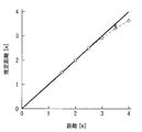
- the broken line in FIG. 10 is the result of examining the relationship between the actual distance from the image sensor to the subject and the distance measurement data according to the method of the invention described in Patent Document 1. It can be seen that in the conventional 3-branch type lock-in pixel, the linearity is beginning to deteriorate from an actual distance of about 3 m.
- the present invention provides a distance measuring device with improved linearity of a distant view and an increased distance measuring range, a camera equipped with the distance measuring device, and a drive adjusting method of the distance measuring device.
- the purpose is to
- a first aspect of the present invention includes (a) a light emitting unit that projects an optical pulse onto an object, (b) a light receiving region that receives reflected light of an optical pulse from the object, and (c) N is 3 or more. Is a positive integer of N, the signal charges photoelectrically converted in the light receiving area are sequentially transferred and transferred along the N charge transfer paths, and (d) charges other than the signal charges are received in the light receiving area.
- a charge discharging gate for discharging from (1), (e) N charge accumulating regions for accumulating the signal charges transferred along the N charge distributing gates, and (f) supplying a control signal to the light emitting unit, And a drive circuit that sequentially supplies a drive signal to each of the N charge distribution gates and the charge discharge gates, and (g) a read amplification circuit that independently reads the signal charges accumulated in the N charge accumulation regions, (h) Input a signal that has passed through the readout amplifier circuit and perform calculations including calculation of the distance to the target object.
- a signal that sequentially expands the charge storage time assigned to a specific charge distribution gate among the N charge distribution gates is generated from the logic operation circuit to be applied and (i) the value output from the logic operation circuit.
- the gist of the present invention is that it is a distance measuring device including a control arithmetic circuit that supplies the driving circuit.
- a second aspect of the present invention provides (p) an imaging optical system, (q) a light emitting unit that projects an optical pulse onto an object, and (r) a reflected light of the optical pulse from the object via the imaging optical system.
- Light-receiving region for receiving light N charge distribution gates for sequentially transferring and transferring signal charges photoelectrically converted in the light-receiving region with N being a positive integer of 3 or more along N charge transfer paths, and charges other than signal charges Are discharged from the light receiving region, N charge accumulation regions for accumulating the signal charges transferred along the N charge distribution gates, respectively, and a control signal is supplied to the light emitting portion and N charge distribution gates are provided.
- a solid-state imaging device that integrates a drive circuit that sequentially supplies a drive signal to each of the division gate and the charge discharge gate, and (s) controls the imaging optical system and inputs a signal that has passed through a read amplification circuit to the target object.
- a logical operation circuit for performing an operation including calculation of a distance of ) A control operation circuit that generates a signal that sequentially extends the charge accumulation time assigned to a specific charge distribution gate among the N charge distribution gates from the value output by the logic operation circuit and supplies the signal to the drive circuit
- the gist is that the camera has.
- a third aspect of the present invention is a light emitting unit that projects a light pulse on an object, a light receiving area that receives reflected light of an optical pulse from the object, N is a positive integer of 3 or more, and photoelectric conversion is performed in the light receiving area.
- N charge distribution gates that sequentially distribute and transfer the signal charges along the N charge transfer paths, the charge discharge gates that discharge charges other than the signal charges from the light receiving region, and the N charge distribution gates.
- a drive circuit that supplies a control signal to the N charge storage regions and the light emitting unit that respectively store the transferred signal charges, and sequentially supplies a drive signal to each of the N charge distribution gates and the charge discharge gates.
- the present invention relates to a drive adjustment method for a distance measuring device that includes a read amplifier circuit that reads out the signal charges accumulated in each charge accumulation region independently.
- the drive adjustment method according to the third aspect of the present invention includes (u) a step of inputting a signal that has passed through a read amplification circuit and performing a calculation including calculation of a distance to an object, and (v) a result of the calculation. , N of the charge distribution gates, a step of generating a signal for sequentially extending the charge accumulation time assigned to a specific charge distribution gate and supplying the signal to the drive circuit.
- the present invention it is possible to provide a distance measuring device in which linearity of a distant view is improved and a distance measuring range is expanded, a camera equipped with this distance measuring device, and a drive adjusting method of the distance measuring device.
- FIG. 3 is a logical block diagram for explaining an internal structure of a control arithmetic circuit included in a peripheral circuit of the distance measuring apparatus according to the first embodiment as a hardware resource. It is a top view explaining the outline of the structure of the three-branch type pixel of the ranging device concerning a 1st embodiment.
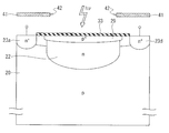
- FIG. 4 is a cross-sectional view seen from the IV-IV direction in FIG. 3.
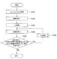
- 3 is a flowchart illustrating an outline of a flow of an adjusting operation by a peripheral circuit of the distance measuring apparatus according to the first embodiment, centered on the control arithmetic circuit shown in FIG. 1.
- FIG. 3 is a flowchart illustrating an outline of a flow of an adjusting operation by a peripheral circuit of the distance measuring apparatus according to the first embodiment, centered on the control arithmetic circuit shown in FIG. 1.
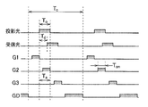
- FIG. 6 is a drive timing diagram illustrating an operation when adjusting the distance measuring device according to the first embodiment.
- FIG. 6 is a drive timing diagram illustrating an operation when adjusting the distance measuring device according to the first embodiment.
- 9 is a flowchart illustrating an outline of an adjusting operation by a peripheral circuit of the distance measuring device according to the reference technique studied before reaching the present invention.
- FIG. 11 is a drive timing diagram illustrating an operation when adjusting the distance measuring device according to the reference technology.
- 6 is a graph showing a relationship between an actual distance and a distance measurement value by the distance measuring device according to the reference technology and the distance measuring device according to the first embodiment of the present invention. It is sectional drawing explaining the behavior of the photoelectron which causes the problem of the ranging device concerning a reference technique.
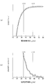
- FIG. 13A is a graph showing the change in the output of G 3 with respect to the charge accumulation time by the distance measuring device according to the first embodiment
- FIG. 13B is the charge accumulation time corresponding to FIG. 13A
- 6 is a graph showing the amount of change (differential) in the output of G 3 with respect to It is a wave form diagram explaining the distance measuring apparatus which concerns on 2nd Embodiment. 6 is a flowchart illustrating an outline of a flow of an adjusting operation by a peripheral circuit of the distance measuring apparatus according to the second embodiment, centering on the control arithmetic circuit shown in FIG. 1.
- FIG. 13A is a graph showing the change in the output of G 3 with respect to the charge accumulation time by the distance measuring device according to the first embodiment
- FIG. 13B is the charge accumulation time corresponding to FIG. 13A
- 6 is a graph showing the amount of change (differential) in the output of G 3 with respect to It is a wave form diagram explaining the distance measuring apparatus which concerns on 2nd Embodiment.
- FIG. 9 is a drive timing diagram for explaining an operation when adjusting the distance measuring device according to the second embodiment. It is a wave form diagram explaining the distance measuring device which concerns on 3rd Embodiment. It is a flow chart explaining an outline of a flow of adjustment operation by a peripheral circuit of a distance measuring device concerning a 3rd embodiment.
- FIG. 11 is a drive timing chart for explaining an operation when adjusting the distance measuring device according to the third embodiment. It is a drive timing diagram explaining operation
- FIG. 22B shows the operation when adjusting the distance measuring apparatus according to the modification of the fourth embodiment, as compared with the drive timing chart according to the fourth embodiment shown in FIG.
- FIG. 6 is a drive timing chart to be described. It is sectional drawing which shows the structure which paid its attention to the photoelectric conversion transfer part of the pixel of the distance measuring device which concerns on the modification of 4th Embodiment.
- FIG. 24B is a drive timing chart for explaining the operation when adjusting the distance measuring apparatus according to the modification of the fourth embodiment, as compared with the drive timing chart according to the reference technique shown in FIG. It is a timing diagram. It is a top view of the principal part of the pixel of the distance measuring device which concerns on 5th Embodiment.
- the first to sixth embodiments exemplify devices and methods for embodying the technical idea of the present invention.
- the technical idea of the present invention is based on the configuration of circuit elements and circuit blocks.
- the layout, the layout on the semiconductor chip, and the like are not specified below.
- the technical idea of the present invention can be variously modified within the technical scope defined by the claims described in the claims.
- the first conductivity type is p-type and the second conductivity type is n-type.
- the first conductivity type is n-type and the second conductivity type is p-type. It can be easily understood that the same effect can be obtained by reversing the electric polarities of the molds. In this case, it goes without saying that the high level and the low level of the pulse waveform may need to be appropriately inverted depending on the common general knowledge of those skilled in the art.
- a distance measuring device based on a 3D image pickup device in which a plurality of pixels (distance measuring elements) are arranged in a two-dimensional matrix in a pixel array portion is shown for convenience of description, but it is merely an example. Not too much.
- a line sensor layout in which distance measuring elements are one-dimensionally arranged as pixels in the pixel array unit may be used.
- the distance sensor may have a simple structure in which only a single distance measuring element is arranged in the pixel array section.
- the distance measuring apparatus includes a pixel array section (X 11 to X 1m ; X 21 to X 2m ; ...; X n1 to X nm ) and peripheral circuits. It is based on a two-dimensional image sensor (3D image pickup device) in which the parts (71, 72, 74 to 77, 94 to 96, NC1 to NCm) are integrated on the same semiconductor chip.
- a two-dimensional image sensor (3D image pickup device) in which the parts (71, 72, 74 to 77, 94 to 96, NC1 to NCm) are integrated on the same semiconductor chip.
- M and n are positive integers of 2 or more, respectively), and form a rectangular imaging region.
- a driving circuit 94 is provided on the upper side of the pixel array section (X 11 to X 1m ; X 21 to X 2m ; ...; X n1 to X nm ) and a horizontal shift register 96 is provided on the lower side. Rows X 11 to X 1m ; X 21 to X 2m ; ...; are provided along the X n1 to X nm direction, and pixel columns X 11 to X n1 ; X 12 to X n2 ; are provided on the right side of the pixel array section.
- the drive circuit 94 is connected to a light emitting unit 91 which serves as a distance measuring element for each pixel X ij and projects the light required for distance measurement as a pulse signal repeatedly.
- a control signal for controlling the drive circuit 94 is transmitted from the control arithmetic circuit (CPU) 74 to the drive circuit 94 via the interface 76.
- the control arithmetic circuit 74 includes a program storage device 77 that stores a program for instructing a series of operations in the control arithmetic circuit 74, and a data storage that stores data, threshold values, etc. necessary for logical operation in the control arithmetic circuit 74.
- the device 72 is connected.
- the control arithmetic circuit 74 is further connected to an output section 75 for outputting the result of the logical operation in the control arithmetic circuit 74.
- Output signals from the pixel array units (X 11 to X 1m ; X 21 to X 2m ; ...; X n1 to X nm ) are input to the data storage device 72 via the output buffers 97 and 98, and the range image is displayed.
- a logical operation circuit 71 is connected to perform an operation including calculation of a distance to an object required for forming the object. Note that, in FIG. 1, as schematically illustrated as an internal structure of the pixel X n1 as a block diagram, each pixel X ij has a signal generation unit 81 including a photoelectric conversion element and a signal charge transfer unit, and a source follower type pixel.
- a read amplifier circuit 82 and the like are included.
- the logical operation circuit 71 uses the equation (5), which will be described later, in addition to the operation of calculating the dark-time equivalent output from the signal measured immediately before, and uses the target object 92 and the pixel array units (X 11 to X 11 ) shown in FIG. 1 m ; X 21 to X 2m ; ...; X n1 to X nm ) and the calculation of the estimated distance L.
- FIG. 1 shows a structure in which the logical operation circuit 71, the interface 76, the control operation circuit 74, the program storage device 77, the data storage device 72, and the output unit 75 are integrated on the same semiconductor chip, this is merely an example. Nothing more than.
- the logic operation circuit 71, the interface 76, the control operation circuit 74, the program storage device 77, the data storage device 72, and at least a part of the circuits of the output unit 75 are separate chips. Alternatively, it may be mounted on a substrate.
- the signal reading from each of the pixels X 11 to X 1m ; X 21 to X 2m ; ...; X n1 to X nm as a distance measuring element is almost the same as that of a normal CMOS image sensor.
- the third drive signal G 3 is simultaneously given to all the pixels X 11 to X 1m ; X 21 to X 2m ; ...; X n1 to X nm from the drive circuit 94, and since it is a high frequency signal, Switching noise occurs during the period. Therefore, signal reading from the pixel portion is performed by providing a reading period after the processing by the noise processing circuits NC1 to NCm is completed.
- the control arithmetic circuit 74 includes a time setting logic circuit 741, a time set value output control circuit 742, a distance image output control circuit 743, a set value determination circuit 744, and a sequence control circuit 745 as hardware.
- the time setting logic circuit 741 sets the values of the light projection time T o and the first charge storage time T a1 , the second charge storage time T a2 , and the third charge storage time T a3 shown in FIG.
- the time setting logic circuit 741 causes the light projection time T o, the first charge accumulation time T a1 , the second charge accumulation time T a2 , and the third charge accumulation time T a1 shown in FIG. This is a logic circuit that appropriately changes the value of the charge storage time T a3 and the like.
- the time setting logic circuit 741 determines that the first drive signal G 1 , the second drive signal G 2 , and the third drive signal G 3 applied to the transfer gate have different timings with an offset time therebetween, as shown in FIG. Set the time so that
- Time setting value output control circuit 742 the repetition period time T c which is set or change the time setting logic circuit 741, the light projection time T o, the first charge accumulation time T a1, the second charge accumulation time T a2, third charge It is a logic circuit that outputs the accumulation time T a3 , the charge transfer time T on, etc. to the drive circuit 94 via the interface 76 as a control signal.
- the distance image output control circuit 743 is a logic circuit which, when the set value determination circuit 744 determines OK, synthesizes the detected value of the distance calculated by the logical operation circuit 71 as the data of the distance image and outputs the data to the output unit 75. .
- the set value determination circuit 744 is the difference between the detected value of the dark equivalent output or distance measured and calculated by the logical operation circuit 71 immediately before, and the detected value of the dark equivalent output or distance measured and calculated at the timing before that. Is a logic circuit that determines whether or not it falls below a threshold value previously stored in the data storage device 72, and outputs the determination result to the time setting logic circuit 741 or the distance image output control circuit 743.
- the sequence control circuit 745 clocks the respective operations of the time setting logic circuit 741, the time set value output control circuit 742, the distance image output control circuit 743, the set value determination circuit 744, the interface 76, the program storage device 77, and the data storage device 72. It is a logic circuit that sequentially controls the sequence depending on a signal. Each of the time setting logic circuit 741, the time setting value output control circuit 742, the distance image output control circuit 743, the setting value determination circuit 744, and the sequence control circuit 745 can send and receive information via the bus 736.
- the data storage device 72 includes a group of registers, a plurality of cache memories, a main storage device, and an auxiliary storage device. It is also possible to make an arbitrary combination appropriately selected from the above. Further, the cache memory may be a combination of a primary cache memory and a secondary cache memory, and may further have a hierarchy including a tertiary cache memory. Although not shown, the bus 736 may be extended to the interface 76, the program storage device 77, the data storage device 72, and the like when the data storage device 72 includes a plurality of registers.
- the control arithmetic circuit 74 shown in FIG. 2 can configure a computer system using a microprocessor (MPU) mounted as a microchip.
- MPU microprocessor
- DSP digital signal processor
- a microcontroller that is equipped with a memory and peripheral circuits for the purpose of controlling embedded equipment ( Microcomputer) etc.
- the main CPU of the current general-purpose computer may be used for the control arithmetic circuit 74.
- control arithmetic circuit 74 may be configured by a programmable logic device (PLD) such as a field programmable gate array (FPGA).
- PLD programmable logic device
- FPGA field programmable gate array
- the data storage device 72 can be configured as a memory element such as a memory block included in a part of the logic block configuring the PLD.
- the control arithmetic circuit 74 may have a structure in which a CPU core-like array and a PLD-like programmable core are mounted on the same chip.
- This CPU-core-like array includes a hard macro CPU pre-installed inside the PLD and a soft macro CPU configured using PLD logic blocks. That is, a configuration in which software processing and hardware processing are mixed inside the PLD may be used.
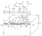
- FIG. 4 shows an example of a sectional structure of the plane structure shown in FIG.
- FIG. 4 is a cross-sectional view as seen from the IV-IV direction of the layout diagram of FIG.
- the gates (32a, 32b), the third charge distribution gates (33a, 33b) and the charge discharging gates (34a, 34b) are connected as an electric field control electrode pair.
- the first charge distribution gate (31a, 31b), the second charge distribution gate (32a, 32b), the third charge distribution gate (33a, 33b) and the charge discharge gate (34a, 34b) receive light.
- the first charge storage region 23a, the second charge storage region 23b, the third charge storage region 23c, and the charge discharge region 23d are diagonally aligned on the gate insulating film 33 from the center position of the light receiving region.
- the light receiving region of the photoelectric conversion element receives the pulsed light that has entered through the opening 42 of the light shielding film 41 as an optical signal, converts this optical signal into a signal charge, and outputs the first charge distribution gate (31a). , 31b), the second charge distribution gates (32a, 32b), and the third charge distribution gates (33a, 33b).
- a functional base layer made of a p-type semiconductor is provided in a portion that functions as the signal generation unit 81 in the pixel of the distance measuring apparatus according to the first embodiment. 20, an n-type surface-embedded region 22 provided in a part of the upper portion of the functional substrate layer 20, and a photoelectric conversion including a p + -type pinning layer 29 provided in contact with the surface of the surface-embedded region 22.
- the region (29, 22) and the gate insulating film 33 provided on the photoelectric conversion region (29, 22) are included.
- the central portion of the photoelectric conversion area (29, 22) is used as a light receiving area.
- n having a higher impurity density than that of the functional base layer 20 is provided so as to surround the light receiving region and to be spaced apart from each other at four positions symmetrical with respect to the center position of the light receiving region.
- a + type first charge storage region 23a, a second charge storage region 23b, a third charge storage region 23c, and a charge discharge region 23d are provided.
- the first charge distribution gates (31a, 31b) of the photoelectric conversion elements forming each pixel are hook-shaped (hook-shaped) first electrostatic induction electrodes 31a and hook-shaped second electrostatic induction electrodes.
- 31b is an electrode pair (electric field control electrode pair) in which a charge transfer path extending diagonally with 31b is sandwiched between them to face each other.
- the second charge distribution gate (32a, 32b) has a hook-shaped third electrostatic induction electrode 32a and a hook-shaped fourth electrostatic induction electrode 32b, and a charge transfer path extending diagonally downward to the left. It is an electrode pair that is sandwiched in an island shape and faces each other.
- the third charge distribution gates (33a, 33b) form a charge transfer path extending diagonally in the upper right direction between the hook-shaped fifth electrostatic induction electrode 33a and the hook-shaped sixth electrostatic induction electrode 33b. , Electrode pairs that are sandwiched in an island shape and face each other.
- the charge discharge gates (34a, 34b) have a hook-shaped seventh electrostatic induction electrode 34a and a hook-shaped eighth electrostatic induction electrode 34b that extend diagonally to the lower right and have charge transfer paths that are island-shaped. It is a pair of electrodes that are sandwiched between and face each other.
- the arrangement topology of the first charge storage region 23a, the second charge storage region 23b, the third charge storage region 23c, and the charge discharge region 23d has a four-fold rotational symmetry with respect to the center position of the light receiving region.
- the pixel of the distance measuring apparatus according to the first embodiment further includes an n-type charge discharging auxiliary region 27a, which has a higher impurity density than the functional base layer 20 in the peripheral portion surrounding the light receiving region.
- 27b, 27c, and 27d are provided apart from each other.
- the first electrostatic induction electrode 31a and the second electrostatic induction electrode 31b are arranged opposite to each other in a mirror image relationship on both sides of the charge transfer path toward the first charge storage region 23a.
- the third electrostatic induction electrode 32a and the fourth electrostatic induction electrode 32b are arranged opposite to each other in a mirror image relationship on both sides of the charge transfer path toward the second charge storage region 23b.
- the fifth electrostatic induction electrode 33a and the sixth electrostatic induction electrode 33b are arranged opposite to each other in a mirror image relationship on both sides of the charge transfer path toward the third charge storage region 23c.
- the seventh electrostatic induction electrode 34a and the eighth electrostatic induction electrode 34b are arranged opposite to each other in a mirror image relationship on both sides of the charge transfer path toward the charge discharging region 23d.
- the pixels of the distance measuring apparatus each include a first charge distribution gate (31a, 31b) and a second charge distribution gate (31a, 31b) that form an electric field control electrode pair.
- 32a, 32b the third charge distribution gates (33a, 33b) and the charge discharge gates (34a, 34b), the first drive signal G 1 , the second drive signal G 2 , the third drive signal G 3 and discharge.
- the drive signal G D is periodically applied as an electric field control pulse, and the depletion potential of the surface-embedded region 22 is alternately changed, so that a potential gradient toward the direction in which charges are transported to one of the charge transfer paths.
- the transfer destinations of the signal charges generated and collected in the surface-embedded region 22 are the first charge accumulation region 23a, the second charge accumulation region 23b, the third charge accumulation region 23c, and the charge discharge region 23d. Sequentially set to either To control.
- the first drive signal G 1 of the first potential level used when setting the charge transfer path By applying a charge discharge pulse having a second potential level larger than the second drive signal G 2 , the third drive signal G 3 , and the discharge drive signal G D to the first charge distribution gate (31a, 31b), It is possible to discharge charges, which are noise current components for distance measurement due to background light (environmental light) or the like, to the charge discharge auxiliary region 27a and the fourth charge discharge auxiliary region 27d.
- the distance is measured to the second charge discharging auxiliary region 27b and the first charge discharging auxiliary region 27a. Can be discharged as a noise current component with respect to.
- the charge discharging pulse of the second potential level is applied to the third charge distribution gates (33a, 33b)
- the third charge discharging auxiliary region 27c and the fourth charge discharging auxiliary region 27d are used for distance measurement. It is possible to discharge the electric charge that becomes the noise current component.
- a noise current component for distance measurement is generated in the second charge discharging auxiliary region 27b and the third charge discharging auxiliary region 27c. Can be discharged.
- the voltage of the first drive signal G 1 , the second drive signal G 2 , the third drive signal G 3 , and the discharge drive signal G D is 2.0 V
- the voltage of the second potential level as the charge discharge pulse is It may be set to about 5V.
- the charge transfer path is set so as to form an X-shape that crosses each other at the center of the light receiving area.
- the distribution gates (33a, 33b) and the charge discharge gates (34a, 34b) the photoelectrons generated in the light receiving region can be accelerated in four directions of X shape by electric field control along the charge transfer path forming the X type.
- the charge modulation can be carried out by moving to.
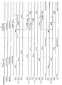
- FIG. 5 is a flowchart showing an outline of an operation related to the control arithmetic circuit 74 of the distance measuring apparatus according to the first embodiment shown in FIG. 1, and FIGS. 6 and 7 are flowcharts shown in FIG. It is the figure which illustrated the drive timing diagram which a drive method changes according to the program used as a flow.
- FIG. 6 is a drive timing chart for explaining the operation at the time of adjustment of the distance measuring apparatus according to the first embodiment.
- the third charge storage time T a3 is shifted according to the value.
- the ON time of the discharge drive signal G D given to the charge discharge gates (34a, 34b) is longer than the pulses of the first drive signal G 1 , the second drive signal G 2 , and the third drive signal G 3 .
- the period in which the pulse of the ejection drive signal G D is turned on / off is the repetition cycle time (T c ).
- the projection light is synchronized with the second charge accumulation time T a2 assigned to the pulse of the second drive signal G 2 in relation to the first drive signal G 1 .
- Distance measurement is performed in a region where received light is obtained during the second charge storage time T a2 assigned to the pulse of the second drive signal G 2 and the third charge storage time T a3 assigned to the pulse of the third drive signal G 3. it can.
- the discharge drive signal G D is a charge discharge gate (34a, 34a, for discharging photoelectrons so that the received light after the third charge accumulation time T a3 assigned to the pulse of the third drive signal G 3 does not become noise in the distance measurement. 34b).
- the first drive signal G 1 is a voltage of a pulse for eliminating (offseting) background light (environmental light), dark current, etc., and the first charge accumulation time T a1 after the discharge drive signal G D is pulsed is It is assigned.
- the effective signal charge Q1 alpha-ef. Transferred and accumulated in the charge accumulation region 23a is the third charge accumulation time in which ⁇ is assigned to the pulse of the third drive signal G 3 in relation to the first drive signal G 1.
- Q1 alpha-ef. ⁇ ⁇ Q1 (3) Given in.
- the distance measuring device according to the first embodiment is suitable for use in an environment where the influence of ambient light is great, such as outdoors or in a bright room.
- c is the speed of light
- T o is the light projection time of the pulse light (pulse width).
- a first auxiliary capacitor C1 and a first source follower amplification transistor SF1 are connected to the first charge storage region 23a via a surface wiring or the like.
- a second auxiliary capacitor C2 and a second source follower amplification transistor SF2 are provided in the second charge storage region 23b
- a third auxiliary capacitor C3 and a third source follower amplification transistor SF2 are provided in the third charge storage region 23c. It is connected to the transistor SF3.
- a power supply VDD is connected to the charge discharging area 23d.
- the set first charge accumulation time T a1 , the second charge accumulation time T a2 , and the third charge accumulation time T a3 are sent to the drive circuit 94 by the time set value output control circuit 742 via the interface 76 shown in FIG. Output as control signal.
- the light emitting section 91 emits pulsed light.
- a near infrared LD laser diode
- a near infrared LED is used.
- the pulsed light reflected by the object 92 passes through the lens 93, a BPF (bandpass filter), etc., and the pixel array section (X 11 to X 1m ; X 21 to X 2m ; ...; X n1 to X nm ) shown in FIG. ) Is irradiated.
- each pixel X ij of the pixel array section controls electrons (photoelectrons) generated by light reception. It operates according to the control signal given from the time setting logic circuit 741 of the arithmetic circuit 74 through the drive circuit 94, and sends the output signal to the logical arithmetic circuit 71 through the output buffer 97.98.
- step S102 the logical operation circuit 71 further sends the distance calculation and the additional operation result to the time setting logic circuit 741 of the control operation circuit 74.
- step S103 of FIG. 5 the time setting logic circuit 741 of the control calculation circuit 74 extends the third charge storage time T a3 .
- the set first charge accumulation time T a1 , the second charge accumulation time T a2 , and the third charge accumulation time T a3 are sent to the drive circuit 94 by the time set value output control circuit 742 via the interface 76 shown in FIG. Output again as a control signal.
- the pulsed light reflected from the light emitting section 91 on the target object 92 to be pulsed is reflected by the lens 93 or the BPF.
- the pixel array section (X 11 to X 1m ; X 21 to X 2m ; ...; X n1 to X nm ) shown in FIG.
- each pixel X ij of the pixel array section controls electrons generated by light reception to the control arithmetic circuit 74. It operates according to the control signal given from the time setting logic circuit 741 through the drive circuit 94, and sends the output signal to the logic operation circuit 71 through the output buffer 97.98.
- Logical operation circuit 71 in step S104 the pixel array portion in response to a signal output from each pixel X ij of (X 11 ⁇ X 1m; X 21 ⁇ X 2m;; ...... X n1 ⁇ X nm), the formula ( 5) is used to calculate the distance, the distance is measured, and the calculation result of the distance and the additional calculation result are sent again to the time setting logic circuit 741.
- the set value determination circuit 744 is one of the third signal charge Q3 corresponding to the dark time which is calculated and calculated by the logical operation circuit 71 immediately before in step S104, It is determined whether or not the difference in the third signal charge Q3 corresponding to the dark time measured and calculated at the previous timing falls below a threshold value stored in the data storage device 72 in advance.
- the difference between the detected value of the distance calculated and calculated immediately before by the logical operation circuit 71 in step S104 and the detected value of the distance measured and calculated one timing before step S104 is It is determined whether or not it falls below a threshold value previously stored in the data storage device 72.
- “corresponding to dark time” means eliminating the influence of ambient light by performing calculations using the equations (1) and (2).
- step S105 when the set value determination circuit 744 determines that the value does not fall below the threshold value (Yes), the data is passed to the time setting logic circuit 741 of the control calculation circuit 74.
- step S106 of FIG. 3 the time setting logic circuit 741 returns to step S104 after the time setting logic circuit 741 of the control arithmetic circuit 74 extends the third charge storage time T a3, and measures the distance again. After that, the loop processing of returning from step S104 to step S105 through step S106 and returning to step S104 is repeated until the set value determination circuit 744 determines that the value is below the threshold value (No) in step S105.
- FIG. 13A shows a change in the third signal charge Q3 corresponding to the dark time with respect to the third charge storage time T a3 at this time.
- the third signal charge Q3 corresponding to the dark time increases so as to approach the certain asymptotic value asymptotically.
- the distance image output control circuit 743 of the control calculation circuit 74 passes the data to the output unit 75, and the output signal is output from the output unit 75. The process shown in FIG. 5 ends.
- FIG. 8 is a flowchart showing an outline of the operation of the distance measuring device according to the reference technique examined by the present inventor before reaching the present invention.
- the reference technique shown in FIG. 8 is a technique for improving the problem of the conventional 3-branch lock-in pixel described in Patent Document 1 and the like.
- the reference technique also follows the processing of the control arithmetic circuit 74 having various logic circuits similar to the hardware resources shown in FIG.
- FIG. 9 is a drive timing chart corresponding to the flow of the flowchart shown in FIG.
- step S901 of FIG. 8 the time setting logic circuit 741 of the control arithmetic circuit 74 sets the light projection time T o to a maximum value. Subsequently, in step S902, the time setting logic circuit 741 sets the repetition cycle time T c to the maximum value.
- the set light projection time T o and repetition period time T c, time setting value output control circuit 742 outputs a control signal to the drive circuit 94 via the interface 76 shown in FIG.
- the light emitting section 91 emits pulsed light.
- the pulsed light reflected by the object 92 is applied to the pixel array section (X 11 to X 1m ; X 21 to X 2m ; ...; X n1 to X nm ) shown in FIG. 1 through the lens 93 and the BPF. .
- each pixel X ij of the pixel array unit responds to the control signal given from the time setting logic circuit 741 of the control arithmetic circuit 74 through the drive circuit 94 to the electron (photoelectron) generated by the light reception. And outputs an output signal to the logical operation circuit 71 via the output buffer 97.98.
- the first drive signal G 1 , the second drive signal G 2 , the third drive signal G 3 , and the discharge drive signal G D are applied at different timings with an offset time in between.
- a first charge distribution gate (31a, 31b) and a second charge distribution gate (32a, 32b), a third charge distribution gate (33a, 33b), and a charge discharge gate, each of which is an electric field control electrode pair. Due to the difference in the signal charge passing through the charge transfer path defined between (34a, 34b), the logical operation circuit 71 executes the operation of calculating the distance using the equation (5) with ⁇ 1 in the equation (3). To do. In step S903, the logic operation circuit 71 further sends the calculation result of the distance calculation to the time setting logic circuit 741 of the control calculation circuit 74.
- step S904 of FIG. 8 the set value determination circuit 744 of the control operation circuit 74 determines whether or not the drive setting is appropriate for the operation result of the distance calculation output from the logical operation circuit 71. If the set value determination circuit 744 determines YES in step S904, the data is passed to the time setting logic circuit 741 of the control calculation circuit 74. Time setting logic 741, in step S905 of FIG. 8, to reduce the light projection time T o. Subsequently, in step S906, the time setting logic circuit 741 shortens the repetition cycle time T c .
- Is shortened light projection time T o and repetition period time T c is the control signal driving method has been changed, via the drive circuit 94 shown in FIG. 1, it is passed to the light-emitting unit 91 and the pixel array unit, in FIG. 8 The distance is measured in step S903. After that, the loop processing that returns to step S903 through step S903, step S904, step S905, and step S906 is repeated until the setting value determination circuit 744 determines NO (No) in step S904. If the set value determination circuit 744 determines no (No), the distance image output control circuit 743 of the control calculation circuit 74 passes the data to the output unit 75 in step S907, and the output signal is output from the output unit 75. .
- the condition is that linearity of about 5 m is obtained, but in the actual measurement result shown by the broken line in FIG. 10, the linearity of the corresponding estimated distance L has been broken from the actual distance of about 3 m.
- the linearity of the distant view collapses as shown by the broken line in FIG.
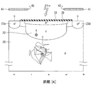
- FIG. 11 is a schematic diagram for explaining the behavior of photoelectrons that causes the linearity of the measured distance with respect to the actual distance to collapse in the distance measuring device according to the reference technology.
- Light (photons) that has passed through the opening 42 of the light shielding film 41 of FIG. 11 is absorbed in the functional base layer 20 to generate photoelectrons (electrons).
- light (photons) is exponentially absorbed from the surface to generate photoelectrons in a one-to-one manner, but in FIG.
- the two photoelectrons generated near the surface-embedded region 22 and relatively deep (far from the surface) of the functional substrate layer 20 and their behavior are shown.
- Photoelectrons generated in a relatively shallow portion of the functional base layer 20 are drift-transported by the electric field applied to the corresponding portion of the functional base layer 20.
- the photoelectrons instantaneously move to the deepest potential portion of the depletion layer generated by the p-type functional base layer 20 and the n-type surface buried region 22, and stand by. After that, if the potential of the charge transfer path defined between the electric field control electrode pairs forming the first charge distribution gates (31a, 31b) shown in FIG. 3 is lowered, photoelectrons are transferred to the first charge storage region 23a. And becomes a signal stored in the first charge storage region 23a.
- photoelectrons generated at a relatively shallow portion of the functional base layer 20 instantaneously move to the deepest potential of the depletion layer generated by the p-type functional base layer 20 and the n-type surface buried region 22 and stand by. If the potential of the charge transfer path defined between the pair of electric field control electrodes forming the charge discharging gates (34a, 34b) shown in FIG. 3 is lowered, the photoelectrons move to the charge discharging region 23d, and the power source (not shown) is supplied. It is discharged to (VDD).
- the photoelectrons generated in the relatively deep portion of the functional base layer 20 do not have an electric field applied in the relatively deep portion of the functional base layer 20, and therefore randomly walk for a while, as schematically shown in FIG. After that, when it reaches a position where an electric field is applied inside the functional base layer 20, due to electric field drift, it instantaneously moves to the deepest potential of the depletion layer generated by the p-type functional base layer 20 and the n-type surface buried region 22. And wait. After that, if the potential of the charge transfer path defined between the electric field control electrode pairs forming the first charge distribution gates (31a, 31b) decreases, the charges move to the first charge storage region 23a, and the first charge storage region 23a moves. The signal is stored in the storage area 23a.
- the photoelectrons generated in a relatively deep portion of the functional base layer 20 randomly walk for a while, and then are instantaneously located at the deepest potential of the depletion layer generated by the p-type functional base layer 20 and the n-type surface buried region 22. Move to and wait.
- the potential of the charge transfer path defined between the electric field control electrode pair forming the charge discharging gates (34a, 34b) is lowered, the photoelectrons move to the charge discharging region 23d and are discharged to a power supply (VDD) not shown. To be done.
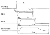
- FIG. 12 is a diagram summarizing an image of a main mechanism causing a problem of the distance measuring device according to the reference technique in the form of a transient response waveform.
- FIG. 12A shows the ideal state.
- T o is a light projection time
- T d is a delay time of received light
- T aeff is a time required for charge storage. If the ideal rectangular projection pulse light is emitted, the reception light having the same shape as the projection pulse light is returned with a delay of T d depending on the distance. Then, if the returned received light is applied to the light receiving portion of the distance measuring device according to the reference technique through the opening 42 of the light shielding film 41, a rectangular photoelectron distribution having the same shape can be obtained.
- FIG. 12B shows a state in which the behavior of photoelectrons in the functional base layer 20 shown in FIG. 11 is taken into consideration.
- T o is the light projection time
- T d is the delay time of the received light
- T aeff is the time required for charge storage
- T oeff is the effective light projection time.
- the third charge storage time T a3 is extended and the time-linear correction of the ambient light is performed. Therefore, the third charge storage region 23c and the third auxiliary capacitor C3 by the ambient light are The sum of the respective charge accumulation amounts increases in proportion to the accumulation time. As a result, the pixel is often saturated by the sum of the charge storage amounts of the third charge storage region 23c and the third auxiliary capacitor C3. In order to improve this, the sum of the charge storage amounts of the third charge storage region 23c and the third auxiliary capacitor C3 is calculated as the sum of the charge storage amounts of the first charge storage region 23a and the first auxiliary capacitor C1. The sum may be designed to be larger than the sum of the charge storage amounts of the second charge storage region 23b and the second auxiliary capacitor C2.
- FIG. 14 is a diagram schematically showing a transient response waveform in the distance measuring apparatus according to the second embodiment.
- a view corresponding to FIG. 14 in the distance measuring apparatus according to the modified examples of the first and first embodiments is shown in FIG.
- the distortion of the waveform of the projection light is not taken into consideration. However, actually, as shown in FIG. 14, the projection light itself is delayed or the waveform is distorted.
- the received light enters after a delay of the distance to the subject.
- the photoelectrons are further delayed than the received light waveform due to the reason described in the modified examples of the first and first embodiments, and the waveform is distorted.
- FIG. 15 is a flowchart showing an outline of the operation of the control arithmetic circuit 74 of the distance measuring device according to the second embodiment.
- the influence of the ambient light can be eliminated by correcting the distance measurement value when the flow is performed by the equations (6) to (9) described later, but it is easier to avoid the influence of the ambient light when the flow is performed, and the accuracy is improved. Therefore, it is desirable to perform the measurement in a dark environment.
- the set first charge accumulation time T a1 , the second charge accumulation time T a2 , and the third charge accumulation time T a3 are sent to the drive circuit 94 by the time set value output control circuit 742 via the interface 76 shown in FIG. Output as control signal.
- the light emitting section 91 emits pulsed light.
- each pixel X ij of the pixel array section controls electrons (photoelectrons) generated by receiving light. It operates according to the control signal given from the time setting logic circuit 741 of the arithmetic circuit 74 through the drive circuit 94, and sends the output signal to the logical arithmetic circuit 71 through the output buffer 97.98.
- step S202 the logic operation circuit 71 further sends the calculation result of the distance calculation to the time setting logic circuit 741 of the control calculation circuit 74.
- step S203 of FIG. 15 the set value determination circuit 744 determines whether or not the first signal charge Q1 corresponding to the dark time does not exceed the threshold value stored in the data storage device 72 in advance. However, the first measurement will not be rejected (No). As shown in FIG. 16, light is emitted in synchronism with the timing of accumulating charges in the second charge accumulation region 23b, and the light emission time is always delayed from the timing of accumulating charges in the second charge accumulation region 23b. In the initial setting, the first signal charge Q1 corresponding to the dark time does not exceed the threshold value since the light emission time is delayed.
- step S203 When the set value determination circuit 744 determines YES in step S203, the data is passed to the time setting logic circuit 741 of the control calculation circuit 74.
- the time setting logic circuit 741 measures the distance in step S202 after the time setting logic circuit 741 of the control operation circuit 74 extends the first charge accumulation time T a1 in step S204 of FIG.
- the loop process of returning to step S202 through step S202, step S203, and step S204 is repeated until the set value determination circuit 744 determines NO in step S203.
- the set value determination circuit 744 determines No, in step S205 the time setting logic circuit 741 of the control operation circuit 74 corresponds to the dark time, which is one cycle or more before the first charge accumulation time T a1 .
- the first signal charge Q1 is reduced to a value when it does not exceed the threshold value, and the process ends.
- the estimated distance L by the distance measuring device according to the second embodiment is expressed by the following equations (6) to (9):
- Q2 real (b) Q2-Q1 beta-ef .... (6)
- Q3 real (b) Q3-Q1 beta-ef .... (7)
- Q1 beta-ef. ⁇ ⁇ Q1 ??
- L (cT o / 2) (Q3 real (b) / (Q2 real (b) + Q3 real (b) )) (9)
- ⁇ is the extension ratio of the first charge accumulation time T a1 .
- the first charge accumulation time T a1 can be extended by using the time setting logic circuit 741 of the control arithmetic circuit 74 shown in FIG.
- the time linear correction of the ambient light may be performed by the extension ratio ⁇ of the first charge accumulation time T a1 .
- the received light that is the distance information signal is not received during the first charge accumulation time T a1 used for ambient light correction, and that the first charge accumulation time T a1 ends as long as possible. That is, it is near the time when the light incidence starts.
- the shortest distance that can be measured on the short distance side does not change, but since the second charge accumulation times T a2 and T a3 can be fully used, the distance measurement range can be expanded.
- the first charge storage time T a1 is extended and the time-linear correction of the ambient light is performed. Therefore, the first charge storage region 23a and the first auxiliary capacitor C1 are affected by the ambient light. The sum of the respective charge accumulation amounts increases in proportion to the accumulation time. As a result, the pixel is often saturated with the sum of the charge storage amounts of the first charge storage region 23a and the first auxiliary capacitor C1. In order to improve this, the sum of the charge storage amounts of the first charge storage region 23a and the first auxiliary capacitor C1 is calculated as the sum of the charge storage amounts of the second charge storage region 23b and the second auxiliary capacitor C2. It may be designed to be larger than the sum of the charge storage amounts of the third charge storage region 23c and the third auxiliary capacitor C3.
- FIGS. 1 to 4 An example of the configuration of the distance measuring device according to the third embodiment is shown in FIGS. 1 to 4, like the distance measuring devices according to the first and second embodiments.
- FIG. 17 is a diagram schematically showing a transient response waveform in the distance measuring apparatus according to the third embodiment.
- FIG. 18 is a flowchart schematically showing the operation of the control calculation circuit 74 of the distance measuring device according to the third embodiment.
- FIG. 19 is a timing diagram based on the flowchart of FIG.
- the waveform shown in FIG. 17 shows a state in which the subject whose distance is desired to be measured is at the shortest distance.
- a flow for extending the second charge storage time T a2 is added to the flowchart of FIG.
- the flow of extending the added second charge storage time T a2 is substantially the same as the flow of extending the third charge storage time T a3 of the distance measuring device according to the first embodiment. That is, the third embodiment is a combination of the first embodiment and the second embodiment, and can improve the linearity of the distant view and expand the range-finding range at the same time.
- the distance measurement value at the time of implementing the flowchart of FIG. 18 can eliminate the influence of ambient light by correction by the following equations (10) to (14). However, when performing the flowchart of FIG. 18, it is easier to avoid the influence of ambient light and the accuracy can be improved. Therefore, it is desirable to perform the measurement in a dark environment.
- ⁇ is the extension rate of the first charge storage time T a1
- ⁇ is the extension rate of the third charge storage time T a3
- the first charge accumulation time T a1 and the third charge accumulation time T a3 can be extended by using the time setting logic circuit 741 of the control arithmetic circuit 74 shown in FIG. Therefore, as shown in Expressions (10) to (14), the time linear correction of the ambient light may be performed with the extension ratio ⁇ of the first charge accumulation time T a1 and the extension ratio ⁇ of the third charge accumulation time T a3. .
- the respective charge storage times are all different from each other, and the distance measurement calculation formula need only be corrected linearly with respect to each charge storage time. That is, in driving the image sensor pixel of the present invention, it is not always necessary that the respective charge storage times be the same, and the respective charge storage times may be changed to be optimum depending on the situation.
- the first charge accumulation region 23a and the first auxiliary by the ambient light are generated.
- the sum of the charge storage amounts of the capacitor C1 and the sum of the charge storage amounts of the third charge storage region 23c and the third auxiliary capacitor C3 increase in proportion to the storage time.
- the pixel is saturated by the sum of the charge storage amounts of the first charge storage region 23a and the first auxiliary capacitor C1 and the sum of the charge storage amounts of the third charge storage region 23c and the third auxiliary capacitor C3. In many cases.
- the sum of the charge storage amounts of the first charge storage region 23a and the first auxiliary capacitor C1 and the sum of the charge storage amounts of the third charge storage region 23c and the third auxiliary capacitor C3. May be designed to be larger than the sum of the charge storage amounts of the second charge storage region 23b and the second auxiliary capacitor C2.
- FIG. 21 shows a sectional view of a main part of a pixel of the distance measuring device according to the fourth embodiment.
- the main part of the pixel is in contact with the surface of the functional base layer 20 made of a p-type semiconductor, the n-type surface-embedded region 22 provided in a part of the upper portion of the functional base layer 20, and the surface-embedded region 22.
- the photoelectric conversion region (29, 22) including the p + -type pinning layer 29 provided and the gate insulating film 33 provided on the photoelectric conversion region (29, 22) are included.
- the central portion of the photoelectric conversion area (29, 22) is used as a light receiving area.
- Impurity density higher than that of the functional base layer 20 is provided so as to surround the photoelectric conversion region (29, 22) at two respective positions symmetrical with respect to the center position of the photoelectric conversion region (29, 22).
- the n + -type first charge accumulation region 23p is arranged as the first floating drain region FD1
- the second charge accumulation region 23q is arranged as the second floating drain region FD2.
- first charge distribution gate 54p (G1) and the second charge distribution gate 54q (G2) which are the two charge distribution gates, have the gate insulating film 33 in the region where the portions other than the opening are shielded by the light shielding film 41. They are connected so as to form a mechanism of a gate type transistor structure.
- the first charge storage region 23p and the second charge storage region 23q are connected as the drain regions of the insulated gate transistors forming the respective charge distribution gates.
- a first auxiliary capacitor C1 and a second auxiliary capacitor C2, and source follower amplification transistors SF1 and SF2 are provided in the first charge storage region 23p and the second charge storage region 23q, respectively, via surface wiring or the like. Connected.
- the channel (charge transfer path) is moved to the floating drain region connected to the transfer gate electrode side where the channel is made conductive.
- the pulsed light is emitted from almost the same position as the image sensor shown in FIG. 21, and the reflected light from the object 92 (see FIG. 1) is received by the image sensor.
- the received light enters the image sensor with a delay time Td from the time when the projection light is emitted, depending on the distance between the object 92 and the image sensor.
- the amount of accumulated charge corresponding to each transfer gate electrode varies depending on the distance between the two, and the distance to the target object 92 can be obtained.
- the received light that has entered the light receiving area of the photoelectric conversion area (29, 22) is delayed. Occurs.
- the photons of the received light are exponentially absorbed from the surface in the photoelectric conversion region (29, 22) and generate photoelectrons in a one-to-one manner.
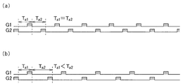
- the charge accumulation time is set to different lengths by using the time setting logic circuit 741 of the control arithmetic circuit 74 shown in FIG. Set. Specifically, like the drive pulse in the first embodiment, the time setting logic circuit 741 charges the second charge storage time T a2 in which the charges are stored in the second charge storage region 23q to the first charge storage region 23p. Is longer than the first charge accumulation time T a1 .
- 20B is a timing diagram showing drive pulses of the distance measuring device according to the fourth embodiment
- FIG. 20A is a timing diagram showing drive pulses of the distance measuring device according to the reference technique.
- the charges that have reached the light receiving region of the photoelectric conversion region (29, 22) are transferred to and accumulated in either the first charge accumulation region 23p or the second charge accumulation region 23q. ing.
- the drive pulse of the distance measuring device according to the reference technology illustrated in FIG. 20A in the case of the distant object 92, the electrons that should enter the second charge storage region 23q are the first charge storage region of the next cycle. Since it enters 23p, the distance accuracy is reduced.
- the drive pulse of the distance measuring device according to the reference technology described in FIG. 20A the electrons that should have entered the second charge accumulation region 23q, which had been included in the first charge accumulation region 23p in the next cycle, are as shown in FIG.
- the drive pulse of the distance measuring apparatus according to the fourth embodiment described in 20 (b) enters the second charge accumulation region 23q without entering the first charge accumulation region 23p in the next cycle.
- the second charge storage time T a2 is lengthened by using the time setting logic circuit 741 of the control arithmetic circuit 74 shown in FIG. Even if the object is far away, the distance accuracy does not decrease.
- FIG. 23 shows a sectional view of a main part of a pixel of a distance measuring device according to a modification of the fourth embodiment.
- the pixel main portion shown in FIG. 23 has a structure in which the third charge distribution gate 54s (G3) is connected to the light receiving region of the photoelectric conversion region (29, 22) of the pixel main portion shown in FIG. .
- a third charge storage region 23s is connected to the third charge distribution gate 54s, and a third auxiliary capacitor C3 (not shown) and a source follower amplification transistor SF3 are connected via a surface wiring or the like.
- a first reset transistor R1, a second reset transistor R2, and a third reset transistor R3 are further connected to the first charge storage region 23p, the second charge storage region 23q, and the third charge storage region 23s, respectively.
- FIG. 22B is a timing diagram showing drive pulses of the distance measuring apparatus according to the modification of the fourth embodiment
- FIG. 22A shows drive pulses of the distance measuring apparatus according to the fourth embodiment. It is a timing diagram.
- the distance measuring device according to the reference technology has a problem that the distance accuracy is reduced when the object is far away. Therefore, in the modification of the fourth embodiment, when the channel (charge transfer path) immediately below the third charge distribution gate 54s is made conductive, the channel (charge transfer path) of the third reset transistor R3 is switched to the conductive state. By setting the conductive state, the charges are discharged to the power supply connected to the reset drain region of the third reset transistor R3 without storing the charges in the third charge accumulation region 23s. Therefore, the electrons that should enter the second charge accumulation region 23q will not enter the first charge accumulation region 23p of the next cycle, and the distance accuracy can be ensured satisfactorily.
- FIG. 25 is a plan view of a main part of a pixel of the distance measuring device according to the fifth embodiment.
- the photogate (PG) 11 having a photoelectric conversion part using a MOS structure having a transparent electrode as a gate electrode is provided so as to be spaced apart from each other at six positions symmetrical with respect to the center position of the photogate 11 so as to surround the photogate (PG) 11.
- the first charge storage region 23p serves as the first floating drain region FD1
- the second charge storage region 23q serves as the second floating drain region FD2
- the third charge storage region 23r serves as the third floating drain region FD3
- the fourth charge storage region The region 23s is the floating drain region FD4, and the first charge discharging region 23u and the second charge discharging region 23v are connected to the power supply VDD.
- a first charge allocating gate 33p (G1) and a second charge allocating gate 33q (G2) are provided so as to surround the periphery of the photogate 11 whose area is defined by shielding the area other than the opening with a light shielding film (not shown).
- the third charge distribution gate 33r (G3), the fourth charge distribution gate 33s (G4), the first charge discharge gate 33u (GD), and the second charge discharge gate 33v (GD) are insulated gate transistor structures, respectively. Are connected as the six transfer gate electrodes that form the mechanism. ..
- the first charge distribution gate 33p, the second charge distribution gate 33q, the third charge distribution gate 33r, the fourth charge distribution gate 33s, the first charge discharge gate 33u, and the second charge are arranged.
- the first charge storage region 23p, the second charge storage region 23q, the third charge storage region 23r, the fourth charge storage region 23s, and the first charge are used as the drain regions of the insulated gate transistors that respectively configure the six charge distribution gates.
- the discharge area 23u and the second charge discharge area 23v are connected. ..
- each of the first charge storage region 23p, the second charge storage region 23q, the third charge storage region 23r, and the fourth charge storage region 23s has a first auxiliary capacitor C1, a second auxiliary capacitor C2, and a second auxiliary capacitor C2.
- the 3rd auxiliary capacitor C3 and the 4th auxiliary capacitor C4 are connected via surface wiring etc., respectively.
- a first source follower amplification transistor SF1, a second source follower amplification transistor SF2 The third source follower amplification transistor SF3 and the fourth source follower amplification transistor SF4 are connected via a surface wiring or the like.
- the first charge discharging area 23u and the second charge discharging area 23v are connected to a power source through surface wiring or the like. ..
- the signal charge or the like collected in the photogate 11 is stored in one of the first charge distribution gate 33p, the second charge distribution gate 33q, the third charge distribution gate 33r, and the fourth charge distribution gate 33s.
- the channel (charge transfer path) moves to the floating drain region connected to the conductive charge distribution gate.
- the channels (charge transfer path) immediately below the first charge discharging gate 33u or the second charge discharging gate 33v is made conductive, charges and the like caused by background light (environmental light) are drained. Is discharged to the power supply via.
- the pulsed light is emitted from almost the same position as the image pickup device shown in FIG. 25, and the reflected light from the object 92 (see FIG. 1) is received by the image pickup device.
- the received light enters the image sensor with a delay of Td from the time when the projection light is emitted, depending on the distance between the object 92 and the image sensor.
- the light projection time T o of the projection light and ON / OFF of the voltage pulse applied to the first charge distribution gate 33p, the second charge distribution gate 33q, the third charge distribution gate 33r or the fourth charge distribution gate 33s. Are synchronized to the first charge accumulation region 23p according to the pulse applied to the first charge distribution gate 33p, and to the second charge accumulation region 23q according to the pulse applied to the second charge distribution gate 33q.
- the delay time Td of the received light is set to the third charge accumulation region 23r according to the pulse applied to the third charge distribution gate 33r, to the fourth charge accumulation region 23s according to the pulse applied to the fourth charge distribution gate 33s. That is, depending on the distance between the distance measuring device and the target object 92, the amount of accumulated charge corresponding to each charge distribution gate varies, and the distance to the target object 92 can be obtained.
- the received light that has entered the light receiving region is delayed even inside the silicon. That is, due to the spread of the photoelectrically converted position, the time collected by the photogate 11 and reaching each of the corresponding charge storage regions via the four charge distribution gates varies, resulting in a delay.
- FIG. 24B is a timing diagram showing drive pulses of the distance measuring device according to the fifth embodiment
- FIG. 24A is a timing diagram showing drive pulses of the distance measuring device according to the reference technique.
- the length of the charge storage time is the same, but the charge storage time may be set to a different length in consideration of the decrease in the distance accuracy due to the delayed signal charge or the like.
- the time setting logic circuit 741 of the control calculation circuit 74 of FIG. 2 as shown in the timing chart of FIG. 24B, it is assigned as the time for accumulating charges in the fourth charge accumulating region 23s.
- the fourth charge storage time T a4 is assigned as the first charge storage time time T a1 which is assigned as the time for storing the charge in the first charge storage region 23p
- the second charge time is assigned as the time for storing the charge in the second charge storage region 23q. It may be set longer than the charge accumulation time T a2 and the third charge accumulation time T a3 assigned as the time for accumulating charges in the third charge accumulation region 23r.
- the rangefinders In the rangefinders according to the first to fifth embodiments, the cases where the number of charge distribution gates serving as the path of the signal charge including the background light (environmental light) component is three and four are described. However, the same argument holds when the number of charge distribution gates serving as the path of the signal charge including the background light (environmental light) component is larger than five. Generally, if N charge distribution gates with N being a positive integer of 3 or more, for example, if the charge accumulation time assigned to the Nth charge distribution gate is lengthened, the first to fifth embodiments are performed. The function and effect similar to those described in the distance measuring device can be realized.
- FIG. 27 shows a plan view of main parts of pixels of the distance measuring device according to the sixth embodiment
- FIG. 26 shows a plan view of main parts of pixels of the distance measuring device according to the reference technology.
- the n + -type first charge storage regions 23p provided separately from each other at four positions symmetrical with respect to the central position of the photodiode 11 having the photoelectric conversion unit using the pn junction are the first floating drains.
- the region FD1 the n + -type second charge storage region 23q serves as the second floating drain region FD2
- the n + -type third charge storage region 23r serves as the third floating drain region FD3, and the n + -type charge discharging region 23s. Is arranged as a drain.
- a first charge distribution gate 54p (G1) which is four charge distribution gates, and a second light distribution gate 54p (G1), so as to surround the photodiode 11 whose region is defined by shielding light other than the opening with a light shielding film (not shown)
- a charge distribution gate 54q (G2), a third charge distribution gate 54r (G3) and a charge discharge gate 54s (GD) are arranged.
- the first charge distribution gate 54p, the second charge distribution gate 54q, the third charge distribution gate 54r, and the charge discharge gate 54s are conductors such as polycrystalline silicon so as to form a mechanism of an insulated gate transistor structure.
- the thin film constitutes the gate electrode.
- the first charge storage region 23p, the second charge storage region 23q, the third charge storage region 23r, and the charge discharge region 23s are connected to the drain region of the insulated gate transistor that constitutes each charge distribution gate.
- a first auxiliary capacitor C1, a second auxiliary capacitor C2, and a third auxiliary capacitor C3 are connected to each of the first charge storage region 23p, the second charge storage region 23q, and the third charge storage region 23r via a surface wiring or the like.
- the first auxiliary capacitor C1 shown in the upper right of FIGS. 26 and 27 is an n + type diffusion region 25p, a capacitor insulating film (not shown) provided on the diffusion region 25p, and a capacitor insulating film on the capacitor insulating film.
- a parallel plate type capacitor can be constituted by the provided first capacitor electrode 38p made of a conductor thin film such as polycrystalline silicon.
- the second auxiliary capacitor C2 shown in the lower right of FIGS. 26 and 27 is an n + type diffusion region 25q, a capacitor insulating film (not shown) provided on the diffusion region 25q, and this capacitor insulation.
- a parallel plate type capacitor can be constituted by the second capacitor electrode 38q made of a conductive thin film such as polycrystalline silicon provided on the film.
- the third auxiliary capacitor C3 shown in the upper left of FIG. 26 is an n + type diffusion region 25r, a capacitor insulating film (not shown) provided on the diffusion region 25r, and a capacitor insulating film provided on the capacitor insulating film.
- the third capacitor electrode 38r made of a conductive thin film such as polycrystalline silicon thus formed constitutes a parallel plate type capacitor.
- the third auxiliary capacitor C3 shown in the upper left of FIG. 27 includes an n + type diffusion region 25R having a larger area than the diffusion region 25r of FIG. 26 and a capacitor insulating film (not shown) provided on the diffusion region 25R. ) And a third capacitor electrode 38r made of a conductor thin film such as polycrystalline silicon provided on the capacitor insulating film, thereby forming a parallel plate type capacitor. Therefore, the third auxiliary capacitor C3 shown in FIG. 27 is about 1.4 times larger than the capacity of the third auxiliary capacitor C3 shown in FIG. 26 and 27, the capacitance of the first auxiliary capacitor C1 and the capacitance of the second auxiliary capacitor C2 are equal.
- the capacitance of the third auxiliary capacitor C3 is equal to that of the first auxiliary capacitor C1 in FIG. It is about 1.4 times the capacity.
- the six white squares shown above the diffusion region 25p, the diffusion region 25q, and the diffusion region 25r each schematically show a contact hole, and diffuse through the surface wiring extending above the contact hole.
- the region 25p, the diffusion region 25q, and the diffusion region 25r are connected to the ground potential (GND).
- first charge storage region 23p, the second charge storage region 23q, and the third charge storage region 23r are used as respective source regions, and a first reset transistor RT having a first gate electrode 53p and a second gate electrode 53q are provided.
- a 3 reset transistor RT having 2 reset transistors RT and a third gate electrode 53r is configured.
- the first gate electrode 53p, the second gate electrode 53q, and the third gate electrode 53r can be composed of a conductor thin film such as polycrystalline silicon.
- the first reset transistor RT has a first reset drain (RD) region 26p facing the first charge storage region 23p via the first gate electrode 53p.
- the second reset transistor RT has a second reset drain (RD) region 26q facing the second charge storage region 23q via the second gate electrode 53q.
- the third reset transistor RT has a third reset drain (RD) region 26r that faces the third charge storage region 23r via the third gate electrode 53r.
- Each of the white squares shown above the first reset drain region 26p, the second reset drain region 26q, and the third reset drain region 26r is a schematic representation of a contact hole, and is above the contact hole.
- the first reset drain region 26p, the second reset drain region 26q, and the third reset drain region 26r are connected to the power supply potential (V DD ) via the surface wiring extending to.
- each of the white squares shown above the first charge storage region 23p, the second charge storage region 23q, and the third charge storage region 23r also schematically shows a contact hole.
- the first charge storage region 23p, the second charge storage region 23q, and the third charge storage region 23r are connected to the first amplification gate electrode 52p of the first source follower amplification transistor SF1 and the second source of the second source via the surface wiring extending upward.
- the second amplification gate electrode 52q of the follower amplification transistor SF2 and the third amplification gate electrode 52r of the third source follower amplification transistor SF3 are connected via a surface wiring or the like.
- the fourth charge storage region 23s is connected to the power supply potential (V DD ) via a surface wiring or the like which runs on a contact hole which is schematically shown by a single white square.
- first charge storage region 23p, the second charge storage region 23p, the second charge storage region 23q, and the third charge storage region 23r via other surface wirings extending above the contact holes, respectively.
- 23q and the third charge storage region 23r are connected to the first capacitor electrode 38p of the first auxiliary capacitor C1, the second capacitor electrode 38q of the second auxiliary capacitor C2, and the third capacitor electrode 38r of the third auxiliary capacitor C3. .
- Illustration of the first amplification drain region 18p of the first source follower amplification transistor SF1, the second amplification drain region 18q of the second source follower amplification transistor SF2, and the third amplification drain region 18r of the third source follower amplification transistor SF3 is omitted.
- the first amplification source region 21p of the first source follower amplification transistor SF1 is connected as a common region to the first drain electrode of the pixel selection first selection transistor SL1.
- the second amplification source region 21q of the second source follower amplification transistor SF2 is connected to the second drain electrode of the second selection transistor SL2 for pixel selection as a common region, and the third amplification of the third source follower amplification transistor SF3 is performed.
- the source region 21r is connected as a common region to the third drain electrode of the third selection transistor SL3 for pixel selection.
- the first selection source region 19p of the first selection transistor SL1 is provided with a first vertical output signal line through a contact hole that is schematically shown by one white square.
- a horizontal line selection control signal S connected to Sig1 and supplied to the first selection gate electrode 51p of the first selection transistor SL1 from the vertical shift register and vertical scanning circuit 95 shown in FIG.
- the second selection source region 19q of the second selection transistor SL2 is connected to the second vertical output signal line Sig2 through one contact hole which is schematically shown by a white square, and A control signal S for selecting a horizontal line is supplied from the vertical shift register and vertical scanning circuit 95 to the second selection gate electrode 51q of the selection transistor SL2.
- the third selection source region 19r of the third selection transistor SL3 is connected to the third vertical output signal line Sig3 through a contact hole that is schematically shown by one white square, and the third selection source region 19r is connected.
- a horizontal line selection control signal S is applied to the third selection gate electrode 51r of the transistor SL3 from the vertical shift register and vertical scanning circuit 95.
- the selection transistors SL1, SL2, SL3 are rendered conductive, and the first charge accumulation regions 23p and the second charge accumulation regions 23q amplified by the source follower amplification transistors SF1, SF2, SF3.
- the first vertical output signal line Sig1, the second vertical output signal line Sig2, and the third vertical output signal line Sig3 are at potentials corresponding to the potential of the third charge storage region 23r.
- the capacitance of the third auxiliary capacitor C3> the capacitance of the first auxiliary capacitor C1 the second auxiliary capacitor C2.
- the charge accumulation time lastly allocated among the charge accumulation times allocated to the plurality of charge distribution gates is lengthened. At this time, due to the ambient light, the sum of the charge storage region connected to the last charge distribution gate having the longer charge storage time and the charge storage amount stored in the auxiliary capacitor increases.
- Saturation of the pixel of the ranging device due to an increase in the sum of the charge storage region connected to the charge distribution gate and the charge storage amount stored in the auxiliary capacitor corresponding to the charge storage time finally allocated Will often be decided.
- the sum of the charge storage area connected to the charge distribution gate corresponding to the last charge allocation time and the capacity of the charge stored in the auxiliary capacitor is added to the charge storage gate connected to another charge distribution gate. It may be designed to be larger than the sum of the capacitances of the charges accumulated in the region and the auxiliary capacitor.
- the third auxiliary capacitor C3 is 1.4 times larger than the first auxiliary capacitor C1 and the second auxiliary capacitor C2 is illustrated, but the third auxiliary capacitor C3 is not limited to 1.4 times, and the environment is not limited to 1.4 times.
- the capacitance value may be appropriately designed in consideration of light intensity and the like.
- the present invention has been described by the first to sixth embodiments, but it should not be understood that the description and drawings forming a part of this disclosure limit the present invention. From this disclosure, various alternative embodiments, examples and operational techniques will be apparent to those skilled in the art.
- the first conductivity type is p-type and the second conductivity type is n-type, but the first conductivity type is n-type and the second conductivity type is n-type. It can be easily understood that the same effect can be obtained by reversing the electric polarities even with the p-type.
- the “charge distribution gate” of the present invention is configured by a pair of lateral electric field control gates (LEFM) with reference to FIG. Indicated.
- LFM lateral electric field control gates
- the structure of the charge distribution gate is the MOS type or MIS type gate electrode structure is illustrated.
- the structure of the charge distribution gate and the charge discharging electrode are not limited to the LEFM and the electrode structure of the insulated gate transistor exemplified in the first to sixth embodiments. Any configuration may be used as long as it has a function of transporting or transferring similar signal charges.
- the photoelectric conversion unit has been described by using the light receiving region forming the pn junction type photodiode.
- the photoelectric conversion section has been described as having a photogate structure using a MOS structure in which a transparent electrode is a gate electrode.
- the photoelectric conversion unit is not limited to the structure of the photodiode or the photogate, and any other structure having a similar photoelectric conversion function may be used.
- the distance measuring devices according to the first to sixth embodiments of the present invention can be used as a 3D image pickup device in the technical field such as a camera illustrated in FIG. 28, for example.
- a camera such as a video camera, which may be used in the technical field, has a single imaging optical system (43, 44) and an optical axis of the imaging optical system (43, 44).
- Used for auto-focusing (AF) and a 3D image pickup device 45a that constitutes a main part of the distance measuring device according to the first to sixth embodiments that picks up an image of an object 92 (see FIG. 1) incident along it.
- a distance sensor (distance measuring element) 15 using the distance measuring device according to the first to sixth embodiments is provided.
- a camera that may utilize the present invention is an A / D that converts image data output from the 3D image pickup device 45a that constitutes the main part of the distance measuring device according to the first to sixth embodiments into digital data.
- a conversion circuit 47 a memory (semiconductor memory device) 48 for storing image data converted into digital data by the A / D conversion circuit 47, a central processing control unit (CPU) 13 for receiving image data from the memory 48, and a central processing unit.
- An image processing unit 14 that receives image data via the processing control unit 13 and processes the image data.
- the image processing unit 14 is connected to an adjustment data storage device 99 ext that stores the adjustment data of the 3D imaging device 45a and the distance sensor (distance measuring element) 15, and the adjustment data storage device 99 ext is shown in FIGS. 5, 8, 15 and 18.
- the adjustment according to the flowchart as illustrated is possible.
- FIG. 28 is merely an example, and an adjustment data storage device that saves the adjustment data transmitted from the central processing control unit 13 on a semiconductor chip on which the 3D image pickup device 45a or the distance sensor (distance measuring element) 15 is mounted is provided.
- the structure may be such that it is connected and supplies adjustment data to the drive circuit on the semiconductor chip.
- a drive unit 12 connected to a central processing control unit 13, a memory card interface 19 such as a media controller, an operation unit 18, an LCD drive circuit 16, a motor driver 13b. , 13c, 13d, and a strobe control circuit 61 can be provided.
- the LCD drive circuit 16 is connected to a display unit 57 composed of an LCD, and the strobe control circuit 61 is connected to a strobe device 62.
- the strobe device 62 can configure the light emitting unit 91 shown in FIG.
- the central processing control unit 13 of the camera illustrated in FIG. 28 includes an image processing unit 14, a driving unit 12, a memory 48, a memory card interface 19, an operation unit 18, an LCD driving circuit 16, which are connected to the central processing control unit 13.
- the distance sensor (distance measuring element) 15, the motor drivers 13b, 13c, 13d and the strobe control device output commands and electric signals for controlling the respective operations and processes.
- the central processing control unit 13 includes an image processing unit 14, a drive unit 12, a memory 48, a memory card interface 19, an operation unit 18, an LCD drive circuit 16, a distance sensor (distance measuring element). 15.
- Various logic circuits such as a command output circuit for executing respective operations of the motor driver 13b, 13c, 13d, and the flash control device, and various logic circuits such as a WB adjustment command output circuit for performing automatic white balance (AWB) adjustment are logical. Is incorporated as a general hardware resource.
- the taking lens 43 constituting the imaging optical system (43, 44) includes, for example, a main lens 43a, a zoom lens 43b adjacent to the main lens 43a, a focus lens 43c adjacent to the zoom lens 43b, and the like. Can be provided.
- the zoom lens 43b is connected to the zoom motor 49b
- the focus lens 43c is connected to the focus motor 49c.
- a diaphragm 44 that constitutes the imaging optical system (43, 44) is arranged between the focus lens 43c and the 3D imaging device 45a.
- an iris motor 50 that drives the diaphragm blades is connected to the diaphragm 44 composed of five diaphragm blades.
- the zoom motor 49b, the focus motor 49c, and the iris motor 50 are stepping motors, operation-controlled by drive pulses transmitted from the motor drivers 13b, 13c, 13d connected to the central processing controller 13, and operation parts such as a release button. Imaging preparation processing is performed by a signal from 18.
- the zoom motor 49b moves the zoom lens 43b toward the wide side or the tele side in, for example, 20 to 50 steps to zoom the photographing lens 43.
- the focus motor 49c moves the focus lens 43c according to the distance from the object 92 and the zooming of the zoom lens 43b, and adjusts the focus of the taking lens 43 so that the imaging conditions of the camera are optimized.
- the iris motor 50 operates the diaphragm blades of the diaphragm 44 to change the aperture area of the diaphragm 44 and appropriately adjust the exposure of the taking lens 43 up to a desired diaphragm value.
- the taking lens 43 is not limited to the configuration illustrated in FIG. 28, and may be, for example, an interchangeable lens that can be attached to and detached from the camera.
- the taking lens 43 is composed of a plurality of optical lens groups such as the main lens 43a, the zoom lens 43b, and the focus lens 43c, so that the light flux from the target object 92 of the 3D imaging device 45a arranged near the focal plane thereof. Image on the surface.
- the 3D imaging device 45a which constitutes the main part of the distance measuring device according to the first to sixth embodiments, is mounted on a chip mounting substrate (package substrate) 46 made of glass or ceramics.
- a timing generator (TG) 63 is connected to the 3D imaging device 45 a, and the timing generator 63 is connected to the central processing control unit 13 via the drive unit 12.
- the timing generator 63 generates a timing signal (clock pulse) in response to a signal sent from the central processing control unit 13 via the drive unit 12, and the timing signal is a semiconductor chip constituting the 3D imaging device 45 a via the chip mounting substrate 46. It is sent to the pixels in each row as an electronic shutter signal from a drive circuit provided above as a peripheral circuit.
- the central processing control unit 13 controls the timing generator 63 via the drive unit 12 to control the shutter speed of the electronic shutter of the 3D imaging device 45a.
- the timing generator 63 may be monolithically integrated as a peripheral circuit on a semiconductor chip that constitutes the 3D imaging device 45a.
- the image pickup signal output from the central pixel array portion of the semiconductor chip that constitutes the 3D image pickup device 45a is input to a correlated double sampling circuit (CDS) provided as a peripheral circuit in the peripheral portion of the semiconductor chip, and is input to the 3D image pickup device.
- CDS correlated double sampling circuit
- the 3D image pickup device 45a outputs R, G, and B image data that accurately correspond to the accumulated charge amount of each pixel of the pixel 45a.
- the image data output from the 3D imaging device 45a is amplified by an amplifier (not shown) and converted into digital data by the A / D conversion circuit 47.
- the 3D image pickup device 45a is timing-controlled by the drive unit 12, and converts the image of the object 92 formed on the light receiving surface of the 3D image pickup device 45a into an image signal and outputs the image signal to the A / D conversion circuit 47.
- the image processing unit 14 of the camera illustrated in FIG. 28 is a WB control amount calculation circuit that calculates a WB control amount used for white balance adjustment, integrates G signals of the entire screen, or centers the screen. G and G signals with different weights are integrated in the peripheral part and the peripheral part and the integrated value is output, and a logical operation circuit for automatic exposure (AE) detection and an integrated value output by the logical operation circuit for AE detection are necessary for AE.
- AE automatic exposure
- a variety of image processing and calculations associated with image processing such as a shooting Ev value calculation circuit that calculates the brightness (shooting Ev value) of the target object 92, a gradation conversion processing circuit, a white balance correction processing circuit, and a ⁇ correction processing circuit. It is also possible to provide various logic circuits (hardware modules) that apply to the image data as hardware resources in a logical configuration.
- the image processing unit 14 can be realized if there is an image processing engine or the like. Further, if the calculation load for the feature amount generation and the identification process is high, the feature amount may be mounted on hardware. For example, it is possible to configure the image processing unit 14 with a computer system using an MPU or the like mounted as a microchip. Further, as the image processing unit 14 included in the computer system, a DSP having an enhanced arithmetic operation function and specialized in signal processing, a microcomputer equipped with a memory or a peripheral circuit for the purpose of controlling an embedded device, and the like may be used. Alternatively, the main CPU of the current general-purpose computer may be used for the image processing unit 14. Further, part or all of the configuration of the image processing unit 14 may be configured by PLD such as FPGA.
- Third capacitor electrode 41 ... Shading film, 42 ... Opening portion, 43 ... Photographing lens, 43a ... Main lens, 43b ... Zoom lens, 43c ... Focus lens, 45a ... 3D image pickup device, 46 ... Chip mounting Substrate, 47 ... A / D conversion circuit, 48 ... Memory, 49b ... Zoom motor, 49c ... Focus motor, 50 ... Iris motor, 51p ... First selection gate electrode, 51q ... Second selection gate electrode, 51r ... Third selection Gate electrode, 52p ... First amplification gate electrode, 52q ... Second amplification gate electrode, 52r ... Third amplification gate electrode, 53p ... First gate electrode, 53 q ... second gate electrode, 53r ... third gate electrode, 54p ...
- first transfer gate electrode 54p ... first charge distribution gate, 54q ... second charge distribution gate, 54r ... third charge distribution gate, 54s Charge discharging gate 57 Display unit 61 Strobe control circuit 62 Strobe device 63 Timing generator 71 Logical operation circuit 72 Data storage device 736 Bus 74 Control operation circuit 741 Time setting logic circuit, 742 ... Time set value output control circuit, 743 ... Distance image output control circuit, 744 ... Set value determination circuit, 745 ... Sequence control circuit, 75 ... Output section, 76 ... Interface, 77 ... Program storage device, 81 ... Signal generation section, 82 ... Read-amplification circuit, 91 ... Light emitting section, 92 ... Object, 93 ... Lens, 94 ... Drive circuit, 95 ... Vertical scanning circuit, 9 ... horizontal shift register, 97, 98 ... output buffer, 99 ext ... adjustment data storage device
Landscapes
- Engineering & Computer Science (AREA)
- Physics & Mathematics (AREA)
- General Physics & Mathematics (AREA)
- Remote Sensing (AREA)
- Radar, Positioning & Navigation (AREA)
- Computer Networks & Wireless Communication (AREA)
- Electromagnetism (AREA)
- Signal Processing (AREA)
- Multimedia (AREA)
- Optical Radar Systems And Details Thereof (AREA)
- Measurement Of Optical Distance (AREA)
- Solid State Image Pick-Up Elements (AREA)
- Transforming Light Signals Into Electric Signals (AREA)
Priority Applications (4)
| Application Number | Priority Date | Filing Date | Title |
|---|---|---|---|
| CN201980067602.XA CN112888958B (zh) | 2018-10-16 | 2019-09-27 | 测距装置、摄像头以及测距装置的驱动调整方法 |
| EP19872289.4A EP3839555A4 (en) | 2018-10-16 | 2019-09-27 | DISTANCE MEASURING DEVICE, CAMERA AND METHOD OF ADJUSTING THE DRIVE OF A DISTANCE MEASURING DEVICE |
| JP2020553015A JP7428133B2 (ja) | 2018-10-16 | 2019-09-27 | 測距装置、カメラ、及び測距装置の駆動調整方法 |
| US17/228,689 US12181609B2 (en) | 2018-10-16 | 2021-04-12 | Distance measuring device, camera, and method for adjusting drive of distance measuring device |
Applications Claiming Priority (2)
| Application Number | Priority Date | Filing Date | Title |
|---|---|---|---|
| JP2018195018 | 2018-10-16 | ||
| JP2018-195018 | 2018-10-16 |
Related Child Applications (1)
| Application Number | Title | Priority Date | Filing Date |
|---|---|---|---|
| US17/228,689 Continuation US12181609B2 (en) | 2018-10-16 | 2021-04-12 | Distance measuring device, camera, and method for adjusting drive of distance measuring device |
Publications (1)
| Publication Number | Publication Date |
|---|---|
| WO2020080065A1 true WO2020080065A1 (ja) | 2020-04-23 |
Family
ID=70284492
Family Applications (1)
| Application Number | Title | Priority Date | Filing Date |
|---|---|---|---|
| PCT/JP2019/038221 Ceased WO2020080065A1 (ja) | 2018-10-16 | 2019-09-27 | 測距装置、カメラ、及び測距装置の駆動調整方法 |
Country Status (5)
| Country | Link |
|---|---|
| US (1) | US12181609B2 (https=) |
| EP (1) | EP3839555A4 (https=) |
| JP (1) | JP7428133B2 (https=) |
| CN (1) | CN112888958B (https=) |
| WO (1) | WO2020080065A1 (https=) |
Cited By (4)
| Publication number | Priority date | Publication date | Assignee | Title |
|---|---|---|---|---|
| WO2021010174A1 (ja) * | 2019-07-16 | 2021-01-21 | ソニー株式会社 | 受光装置、および、受光装置の駆動方法 |
| JP2022100820A (ja) * | 2020-12-24 | 2022-07-06 | 凸版印刷株式会社 | 距離画像撮像装置、及び距離画像撮像方法 |
| JP2022162392A (ja) * | 2021-04-12 | 2022-10-24 | 凸版印刷株式会社 | 距離画像撮像装置、及び距離画像撮像方法 |
| US12181609B2 (en) | 2018-10-16 | 2024-12-31 | Toppan Holdings Inc. | Distance measuring device, camera, and method for adjusting drive of distance measuring device |
Families Citing this family (6)
| Publication number | Priority date | Publication date | Assignee | Title |
|---|---|---|---|---|
| WO2017149932A1 (ja) * | 2016-03-03 | 2017-09-08 | ソニー株式会社 | 医療用画像処理装置、システム、方法及びプログラム |
| US11205279B2 (en) * | 2019-12-13 | 2021-12-21 | Sony Semiconductor Solutions Corporation | Imaging devices and decoding methods thereof |
| TWI757213B (zh) * | 2021-07-14 | 2022-03-01 | 神煜電子股份有限公司 | 具線性電偏移校正的近接感測裝置 |
| JP2024542469A (ja) * | 2021-11-26 | 2024-11-15 | ソニーセミコンダクタソリューションズ株式会社 | 飛行時間型回路および飛行時間方法 |
| WO2023224077A1 (ja) * | 2022-05-18 | 2023-11-23 | 株式会社小糸製作所 | ToFカメラ、車両用センシングシステム、および車両用灯具 |
| JP2026022856A (ja) * | 2024-07-31 | 2026-02-13 | Toppanホールディングス株式会社 | 距離画像撮像素子、及び距離画像撮像装置 |
Citations (6)
| Publication number | Priority date | Publication date | Assignee | Title |
|---|---|---|---|---|
| DE4305011A1 (de) * | 1993-02-18 | 1994-08-25 | Deutsche Aerospace | Pulslaufzeit-Meßverfahren |
| WO2007026779A1 (ja) | 2005-08-30 | 2007-03-08 | National University Corporation Shizuoka University | 半導体測距素子及び固体撮像装置 |
| JP2010267720A (ja) * | 2009-05-13 | 2010-11-25 | Denso Corp | 受光デバイス及びその制御方法 |
| JP2015049148A (ja) * | 2013-09-02 | 2015-03-16 | 株式会社メガチップス | 距離測定装置 |
| JP2016045066A (ja) * | 2014-08-22 | 2016-04-04 | 浜松ホトニクス株式会社 | 測距方法及び測距装置 |
| WO2017022219A1 (ja) * | 2015-08-04 | 2017-02-09 | パナソニックIpマネジメント株式会社 | 固体撮像装置の駆動方法 |
Family Cites Families (13)
| Publication number | Priority date | Publication date | Assignee | Title |
|---|---|---|---|---|
| US5486711A (en) * | 1993-06-25 | 1996-01-23 | Nikon Corporation | Solid-state image sensor with overlapping split gate electrodes |
| JP4235729B2 (ja) * | 2003-02-03 | 2009-03-11 | 国立大学法人静岡大学 | 距離画像センサ |
| WO2008152647A2 (en) * | 2007-06-15 | 2008-12-18 | Ben Gurion University Of The Negev Research And Development Authority | Three-dimensional imaging method and apparatus |
| EP2320460B1 (en) * | 2008-08-11 | 2013-03-13 | Honda Motor Co., Ltd. | Pixel, pixel forming method, imaging device and image forming method |
| US10230914B2 (en) * | 2014-02-07 | 2019-03-12 | National University Corporation Shizuoka University | Charge modulation element and solid-state imaging device |
| CN107533136B (zh) * | 2015-06-24 | 2020-08-25 | 株式会社村田制作所 | 距离传感器 |
| WO2017022218A1 (ja) * | 2015-08-04 | 2017-02-09 | パナソニックIpマネジメント株式会社 | 固体撮像装置 |
| US10620300B2 (en) * | 2015-08-20 | 2020-04-14 | Apple Inc. | SPAD array with gated histogram construction |
| JP6852416B2 (ja) * | 2016-03-10 | 2021-03-31 | 株式会社リコー | 距離測定装置、移動体、ロボット、装置及び3次元計測方法 |
| US10636822B2 (en) * | 2016-08-24 | 2020-04-28 | National University Corporation Shizuoka University | Photoelectric conversion element and solid-state image capturing device |
| EP3550330B1 (en) * | 2016-11-29 | 2022-05-04 | Nuvoton Technology Corporation Japan | Distance measuring device |
| JP7363782B2 (ja) | 2018-07-02 | 2023-10-18 | Toppanホールディングス株式会社 | 測距装置、カメラ、検査調整装置、測距装置の駆動調整方法及び検査調整方法 |
| WO2020080065A1 (ja) | 2018-10-16 | 2020-04-23 | 株式会社ブルックマンテクノロジ | 測距装置、カメラ、及び測距装置の駆動調整方法 |
-
2019
- 2019-09-27 WO PCT/JP2019/038221 patent/WO2020080065A1/ja not_active Ceased
- 2019-09-27 EP EP19872289.4A patent/EP3839555A4/en active Pending
- 2019-09-27 JP JP2020553015A patent/JP7428133B2/ja active Active
- 2019-09-27 CN CN201980067602.XA patent/CN112888958B/zh active Active
-
2021
- 2021-04-12 US US17/228,689 patent/US12181609B2/en active Active
Patent Citations (6)
| Publication number | Priority date | Publication date | Assignee | Title |
|---|---|---|---|---|
| DE4305011A1 (de) * | 1993-02-18 | 1994-08-25 | Deutsche Aerospace | Pulslaufzeit-Meßverfahren |
| WO2007026779A1 (ja) | 2005-08-30 | 2007-03-08 | National University Corporation Shizuoka University | 半導体測距素子及び固体撮像装置 |
| JP2010267720A (ja) * | 2009-05-13 | 2010-11-25 | Denso Corp | 受光デバイス及びその制御方法 |
| JP2015049148A (ja) * | 2013-09-02 | 2015-03-16 | 株式会社メガチップス | 距離測定装置 |
| JP2016045066A (ja) * | 2014-08-22 | 2016-04-04 | 浜松ホトニクス株式会社 | 測距方法及び測距装置 |
| WO2017022219A1 (ja) * | 2015-08-04 | 2017-02-09 | パナソニックIpマネジメント株式会社 | 固体撮像装置の駆動方法 |
Non-Patent Citations (1)
| Title |
|---|
| See also references of EP3839555A4 |
Cited By (6)
| Publication number | Priority date | Publication date | Assignee | Title |
|---|---|---|---|---|
| US12181609B2 (en) | 2018-10-16 | 2024-12-31 | Toppan Holdings Inc. | Distance measuring device, camera, and method for adjusting drive of distance measuring device |
| WO2021010174A1 (ja) * | 2019-07-16 | 2021-01-21 | ソニー株式会社 | 受光装置、および、受光装置の駆動方法 |
| JP2022100820A (ja) * | 2020-12-24 | 2022-07-06 | 凸版印刷株式会社 | 距離画像撮像装置、及び距離画像撮像方法 |
| JP7739709B2 (ja) | 2020-12-24 | 2025-09-17 | Toppanホールディングス株式会社 | 距離画像撮像装置、及び距離画像撮像方法 |
| JP2022162392A (ja) * | 2021-04-12 | 2022-10-24 | 凸版印刷株式会社 | 距離画像撮像装置、及び距離画像撮像方法 |
| JP7635618B2 (ja) | 2021-04-12 | 2025-02-26 | Toppanホールディングス株式会社 | 距離画像撮像装置、及び距離画像撮像方法 |
Also Published As
| Publication number | Publication date |
|---|---|
| CN112888958B (zh) | 2024-10-15 |
| EP3839555A1 (en) | 2021-06-23 |
| CN112888958A (zh) | 2021-06-01 |
| JP7428133B2 (ja) | 2024-02-06 |
| EP3839555A4 (en) | 2022-07-06 |
| US12181609B2 (en) | 2024-12-31 |
| JPWO2020080065A1 (ja) | 2021-09-24 |
| US20210255286A1 (en) | 2021-08-19 |
Similar Documents
| Publication | Publication Date | Title |
|---|---|---|
| JP7428133B2 (ja) | 測距装置、カメラ、及び測距装置の駆動調整方法 | |
| CN111466029B (zh) | 用于计算机视觉应用的全局快门像素电路和方法 | |
| JP6039165B2 (ja) | 撮像素子及び撮像装置 | |
| US8159580B2 (en) | Solid-state imaging device and imaging apparatus using the same | |
| CN112639513B (zh) | 测距装置、照相机、检查调整装置、测距装置的驱动调整方法及检查调整方法 | |
| TWI232678B (en) | Solid-state imaging apparatus and driving method thereof | |
| JP7591095B2 (ja) | 撮像装置 | |
| CN107924927A (zh) | 固体摄像装置 | |
| US20090028538A1 (en) | Solid-state image sensor and automatic-focus camera using the same | |
| KR20090086091A (ko) | 고체 촬상 장치, 고체 촬상 장치의 구동 방법 및 촬상 장치 | |
| JP2012217059A (ja) | 固体撮像装置 | |
| US20140239430A1 (en) | Solid-state imaging device | |
| JP2003198948A (ja) | 固体撮像装置および固体撮像装置の駆動方法 | |
| WO2016047474A1 (ja) | 固体撮像装置、および電子装置 | |
| JP2015207594A (ja) | 固体撮像装置 | |
| JP2008283593A (ja) | 固体撮像装置 | |
| JP5187039B2 (ja) | 固体撮像装置及びこれを用いた電子カメラ | |
| WO2015170533A1 (ja) | 固体撮像装置、固体撮像装置の駆動方法、及び、電子機器 | |
| JP7358771B2 (ja) | 3d撮像ユニット、カメラ、及び3d画像生成方法 | |
| JP4375339B2 (ja) | 固体撮像装置および固体撮像装置の駆動方法 | |
| JP2017108275A (ja) | 固体撮像装置、固体撮像装置の制御方法、および撮像システム | |
| JP7726241B2 (ja) | 撮像素子および撮像装置 | |
| TWI543618B (zh) | 像素電路 | |
| JPH05161075A (ja) | 固体撮像装置 | |
| JPH05161071A (ja) | 固体撮像装置 |
Legal Events
| Date | Code | Title | Description |
|---|---|---|---|
| 121 | Ep: the epo has been informed by wipo that ep was designated in this application |
Ref document number: 19872289 Country of ref document: EP Kind code of ref document: A1 |
|
| ENP | Entry into the national phase |
Ref document number: 2020553015 Country of ref document: JP Kind code of ref document: A |
|
| ENP | Entry into the national phase |
Ref document number: 2019872289 Country of ref document: EP Effective date: 20210318 |
|
| NENP | Non-entry into the national phase |
Ref country code: DE |