WO2020066024A1 - Dispositif d'affichage et son procédé d'attaque - Google Patents
Dispositif d'affichage et son procédé d'attaque Download PDFInfo
- Publication number
- WO2020066024A1 WO2020066024A1 PCT/JP2018/036597 JP2018036597W WO2020066024A1 WO 2020066024 A1 WO2020066024 A1 WO 2020066024A1 JP 2018036597 W JP2018036597 W JP 2018036597W WO 2020066024 A1 WO2020066024 A1 WO 2020066024A1
- Authority
- WO
- WIPO (PCT)
- Prior art keywords
- threshold control
- voltage
- threshold
- transistor
- pixel circuit
- Prior art date
Links
Images


Classifications
-
- G—PHYSICS
- G09—EDUCATION; CRYPTOGRAPHY; DISPLAY; ADVERTISING; SEALS
- G09G—ARRANGEMENTS OR CIRCUITS FOR CONTROL OF INDICATING DEVICES USING STATIC MEANS TO PRESENT VARIABLE INFORMATION
- G09G3/00—Control arrangements or circuits, of interest only in connection with visual indicators other than cathode-ray tubes
- G09G3/20—Control arrangements or circuits, of interest only in connection with visual indicators other than cathode-ray tubes for presentation of an assembly of a number of characters, e.g. a page, by composing the assembly by combination of individual elements arranged in a matrix no fixed position being assigned to or needed to be assigned to the individual characters or partial characters
- G09G3/22—Control arrangements or circuits, of interest only in connection with visual indicators other than cathode-ray tubes for presentation of an assembly of a number of characters, e.g. a page, by composing the assembly by combination of individual elements arranged in a matrix no fixed position being assigned to or needed to be assigned to the individual characters or partial characters using controlled light sources
- G09G3/30—Control arrangements or circuits, of interest only in connection with visual indicators other than cathode-ray tubes for presentation of an assembly of a number of characters, e.g. a page, by composing the assembly by combination of individual elements arranged in a matrix no fixed position being assigned to or needed to be assigned to the individual characters or partial characters using controlled light sources using electroluminescent panels
- G09G3/32—Control arrangements or circuits, of interest only in connection with visual indicators other than cathode-ray tubes for presentation of an assembly of a number of characters, e.g. a page, by composing the assembly by combination of individual elements arranged in a matrix no fixed position being assigned to or needed to be assigned to the individual characters or partial characters using controlled light sources using electroluminescent panels semiconductive, e.g. using light-emitting diodes [LED]
- G09G3/3208—Control arrangements or circuits, of interest only in connection with visual indicators other than cathode-ray tubes for presentation of an assembly of a number of characters, e.g. a page, by composing the assembly by combination of individual elements arranged in a matrix no fixed position being assigned to or needed to be assigned to the individual characters or partial characters using controlled light sources using electroluminescent panels semiconductive, e.g. using light-emitting diodes [LED] organic, e.g. using organic light-emitting diodes [OLED]
- G09G3/3225—Control arrangements or circuits, of interest only in connection with visual indicators other than cathode-ray tubes for presentation of an assembly of a number of characters, e.g. a page, by composing the assembly by combination of individual elements arranged in a matrix no fixed position being assigned to or needed to be assigned to the individual characters or partial characters using controlled light sources using electroluminescent panels semiconductive, e.g. using light-emitting diodes [LED] organic, e.g. using organic light-emitting diodes [OLED] using an active matrix
- G09G3/3233—Control arrangements or circuits, of interest only in connection with visual indicators other than cathode-ray tubes for presentation of an assembly of a number of characters, e.g. a page, by composing the assembly by combination of individual elements arranged in a matrix no fixed position being assigned to or needed to be assigned to the individual characters or partial characters using controlled light sources using electroluminescent panels semiconductive, e.g. using light-emitting diodes [LED] organic, e.g. using organic light-emitting diodes [OLED] using an active matrix with pixel circuitry controlling the current through the light-emitting element
-
- G—PHYSICS
- G09—EDUCATION; CRYPTOGRAPHY; DISPLAY; ADVERTISING; SEALS
- G09G—ARRANGEMENTS OR CIRCUITS FOR CONTROL OF INDICATING DEVICES USING STATIC MEANS TO PRESENT VARIABLE INFORMATION
- G09G3/00—Control arrangements or circuits, of interest only in connection with visual indicators other than cathode-ray tubes
- G09G3/20—Control arrangements or circuits, of interest only in connection with visual indicators other than cathode-ray tubes for presentation of an assembly of a number of characters, e.g. a page, by composing the assembly by combination of individual elements arranged in a matrix no fixed position being assigned to or needed to be assigned to the individual characters or partial characters
- G09G3/22—Control arrangements or circuits, of interest only in connection with visual indicators other than cathode-ray tubes for presentation of an assembly of a number of characters, e.g. a page, by composing the assembly by combination of individual elements arranged in a matrix no fixed position being assigned to or needed to be assigned to the individual characters or partial characters using controlled light sources
- G09G3/30—Control arrangements or circuits, of interest only in connection with visual indicators other than cathode-ray tubes for presentation of an assembly of a number of characters, e.g. a page, by composing the assembly by combination of individual elements arranged in a matrix no fixed position being assigned to or needed to be assigned to the individual characters or partial characters using controlled light sources using electroluminescent panels
- G09G3/32—Control arrangements or circuits, of interest only in connection with visual indicators other than cathode-ray tubes for presentation of an assembly of a number of characters, e.g. a page, by composing the assembly by combination of individual elements arranged in a matrix no fixed position being assigned to or needed to be assigned to the individual characters or partial characters using controlled light sources using electroluminescent panels semiconductive, e.g. using light-emitting diodes [LED]
- G09G3/3208—Control arrangements or circuits, of interest only in connection with visual indicators other than cathode-ray tubes for presentation of an assembly of a number of characters, e.g. a page, by composing the assembly by combination of individual elements arranged in a matrix no fixed position being assigned to or needed to be assigned to the individual characters or partial characters using controlled light sources using electroluminescent panels semiconductive, e.g. using light-emitting diodes [LED] organic, e.g. using organic light-emitting diodes [OLED]
- G09G3/3266—Details of drivers for scan electrodes
-
- G—PHYSICS
- G09—EDUCATION; CRYPTOGRAPHY; DISPLAY; ADVERTISING; SEALS
- G09G—ARRANGEMENTS OR CIRCUITS FOR CONTROL OF INDICATING DEVICES USING STATIC MEANS TO PRESENT VARIABLE INFORMATION
- G09G3/00—Control arrangements or circuits, of interest only in connection with visual indicators other than cathode-ray tubes
- G09G3/20—Control arrangements or circuits, of interest only in connection with visual indicators other than cathode-ray tubes for presentation of an assembly of a number of characters, e.g. a page, by composing the assembly by combination of individual elements arranged in a matrix no fixed position being assigned to or needed to be assigned to the individual characters or partial characters
- G09G3/22—Control arrangements or circuits, of interest only in connection with visual indicators other than cathode-ray tubes for presentation of an assembly of a number of characters, e.g. a page, by composing the assembly by combination of individual elements arranged in a matrix no fixed position being assigned to or needed to be assigned to the individual characters or partial characters using controlled light sources
- G09G3/30—Control arrangements or circuits, of interest only in connection with visual indicators other than cathode-ray tubes for presentation of an assembly of a number of characters, e.g. a page, by composing the assembly by combination of individual elements arranged in a matrix no fixed position being assigned to or needed to be assigned to the individual characters or partial characters using controlled light sources using electroluminescent panels
- G09G3/32—Control arrangements or circuits, of interest only in connection with visual indicators other than cathode-ray tubes for presentation of an assembly of a number of characters, e.g. a page, by composing the assembly by combination of individual elements arranged in a matrix no fixed position being assigned to or needed to be assigned to the individual characters or partial characters using controlled light sources using electroluminescent panels semiconductive, e.g. using light-emitting diodes [LED]
- G09G3/3208—Control arrangements or circuits, of interest only in connection with visual indicators other than cathode-ray tubes for presentation of an assembly of a number of characters, e.g. a page, by composing the assembly by combination of individual elements arranged in a matrix no fixed position being assigned to or needed to be assigned to the individual characters or partial characters using controlled light sources using electroluminescent panels semiconductive, e.g. using light-emitting diodes [LED] organic, e.g. using organic light-emitting diodes [OLED]
- G09G3/3275—Details of drivers for data electrodes
-
- G—PHYSICS
- G09—EDUCATION; CRYPTOGRAPHY; DISPLAY; ADVERTISING; SEALS
- G09G—ARRANGEMENTS OR CIRCUITS FOR CONTROL OF INDICATING DEVICES USING STATIC MEANS TO PRESENT VARIABLE INFORMATION
- G09G2300/00—Aspects of the constitution of display devices
- G09G2300/04—Structural and physical details of display devices
- G09G2300/0421—Structural details of the set of electrodes
- G09G2300/043—Compensation electrodes or other additional electrodes in matrix displays related to distortions or compensation signals, e.g. for modifying TFT threshold voltage in column driver
-
- G—PHYSICS
- G09—EDUCATION; CRYPTOGRAPHY; DISPLAY; ADVERTISING; SEALS
- G09G—ARRANGEMENTS OR CIRCUITS FOR CONTROL OF INDICATING DEVICES USING STATIC MEANS TO PRESENT VARIABLE INFORMATION
- G09G2300/00—Aspects of the constitution of display devices
- G09G2300/08—Active matrix structure, i.e. with use of active elements, inclusive of non-linear two terminal elements, in the pixels together with light emitting or modulating elements
- G09G2300/0809—Several active elements per pixel in active matrix panels
- G09G2300/0819—Several active elements per pixel in active matrix panels used for counteracting undesired variations, e.g. feedback or autozeroing
-
- G—PHYSICS
- G09—EDUCATION; CRYPTOGRAPHY; DISPLAY; ADVERTISING; SEALS
- G09G—ARRANGEMENTS OR CIRCUITS FOR CONTROL OF INDICATING DEVICES USING STATIC MEANS TO PRESENT VARIABLE INFORMATION
- G09G2300/00—Aspects of the constitution of display devices
- G09G2300/08—Active matrix structure, i.e. with use of active elements, inclusive of non-linear two terminal elements, in the pixels together with light emitting or modulating elements
- G09G2300/0809—Several active elements per pixel in active matrix panels
- G09G2300/0842—Several active elements per pixel in active matrix panels forming a memory circuit, e.g. a dynamic memory with one capacitor
- G09G2300/0852—Several active elements per pixel in active matrix panels forming a memory circuit, e.g. a dynamic memory with one capacitor being a dynamic memory with more than one capacitor
-
- G—PHYSICS
- G09—EDUCATION; CRYPTOGRAPHY; DISPLAY; ADVERTISING; SEALS
- G09G—ARRANGEMENTS OR CIRCUITS FOR CONTROL OF INDICATING DEVICES USING STATIC MEANS TO PRESENT VARIABLE INFORMATION
- G09G2310/00—Command of the display device
- G09G2310/02—Addressing, scanning or driving the display screen or processing steps related thereto
- G09G2310/0202—Addressing of scan or signal lines
- G09G2310/0213—Addressing of scan or signal lines controlling the sequence of the scanning lines with respect to the patterns to be displayed, e.g. to save power
-
- G—PHYSICS
- G09—EDUCATION; CRYPTOGRAPHY; DISPLAY; ADVERTISING; SEALS
- G09G—ARRANGEMENTS OR CIRCUITS FOR CONTROL OF INDICATING DEVICES USING STATIC MEANS TO PRESENT VARIABLE INFORMATION
- G09G2310/00—Command of the display device
- G09G2310/06—Details of flat display driving waveforms
- G09G2310/061—Details of flat display driving waveforms for resetting or blanking
-
- G—PHYSICS
- G09—EDUCATION; CRYPTOGRAPHY; DISPLAY; ADVERTISING; SEALS
- G09G—ARRANGEMENTS OR CIRCUITS FOR CONTROL OF INDICATING DEVICES USING STATIC MEANS TO PRESENT VARIABLE INFORMATION
- G09G2320/00—Control of display operating conditions
- G09G2320/02—Improving the quality of display appearance
- G09G2320/0247—Flicker reduction other than flicker reduction circuits used for single beam cathode-ray tubes
-
- G—PHYSICS
- G09—EDUCATION; CRYPTOGRAPHY; DISPLAY; ADVERTISING; SEALS
- G09G—ARRANGEMENTS OR CIRCUITS FOR CONTROL OF INDICATING DEVICES USING STATIC MEANS TO PRESENT VARIABLE INFORMATION
- G09G2320/00—Control of display operating conditions
- G09G2320/10—Special adaptations of display systems for operation with variable images
-
- G—PHYSICS
- G09—EDUCATION; CRYPTOGRAPHY; DISPLAY; ADVERTISING; SEALS
- G09G—ARRANGEMENTS OR CIRCUITS FOR CONTROL OF INDICATING DEVICES USING STATIC MEANS TO PRESENT VARIABLE INFORMATION
- G09G2330/00—Aspects of power supply; Aspects of display protection and defect management
- G09G2330/02—Details of power systems and of start or stop of display operation
- G09G2330/021—Power management, e.g. power saving
Definitions
- the present invention relates to a display device, and more particularly, to a current-driven display device including a current-driven display element such as an organic EL (Electro Luminescence) display device and a driving method thereof.
- a current-driven display device including a current-driven display element such as an organic EL (Electro Luminescence) display device and a driving method thereof.
- an organic EL display device including a pixel circuit including an organic EL element (also referred to as an organic light emitting diode (Organic Light Emitting Diode: OLED)) has been put to practical use.
- the pixel circuit of the organic EL display device includes a drive transistor, a write control transistor, a holding capacitor, and the like, in addition to the organic EL element.
- a thin film transistor Thin Film Transistor
- a storage capacitor is connected to a gate terminal as a control terminal of the drive transistor.
- the storage capacitor is connected to the drive circuit via a data signal line.
- a voltage corresponding to a video signal representing an image to be displayed (more specifically, a voltage indicating a gradation value of a pixel to be formed by the pixel circuit) is provided as a data voltage.
- the organic EL element is a self-luminous display element that emits light at a luminance according to the current flowing through the organic EL element.
- the drive transistor is provided in series with the organic EL element, and controls a current flowing through the organic EL element according to a voltage held by the storage capacitor.
- a display device that performs pause driving (also called intermittent driving or low-frequency driving) is known as a display device with low power consumption.
- a drive period (refresh period) and a pause period (non-refresh period) are provided when the same image is continuously displayed, and the drive circuit is operated during the drive period, and the operation of the drive circuit is stopped during the pause period. It is a driving method.
- the pause drive can be applied when the transistor in the pixel circuit has good off-leak characteristics (off-leak current is small).
- a display device that performs a pause drive is described in, for example, Japanese Patent Application Laid-Open No. H10-157,036.
- the pixel circuit initializes, for example, the voltage of the gate terminal of the driving transistor, that is, the voltage held in the holding capacitor, to a predetermined level. Thereafter, the storage capacitor is charged with the data voltage via the driving transistor in the diode connection state.
- an initialization transistor for initializing a voltage held in the holding capacitor is provided, and one terminal of the holding capacitor (a terminal connected to the gate terminal of the driving transistor) is connected to the initializing transistor. Connected to a supply line of the initialization voltage via the reset transistor.
- the luminance of the organic EL element decreases or increases in the pause period, and the luminance of the organic EL element returns to the original luminance every time the drive period starts.
- the length of the pause period is much longer than the normal frame period (1/60 second), and the driving frequency of the display device is substantially lower than that of the normal drive (for example, 10 Hz or less).
- the driving frequency is greatly reduced by the pause driving, the luminance change of the organic EL element caused by the repetition of the pause period and the driving period is visually recognized as flicker.
- a display device includes a plurality of data signal lines, a plurality of scanning signal lines intersecting the plurality of data signal lines, the plurality of data signal lines, and the plurality of scanning signal lines.
- a plurality of pixel circuits arranged in a matrix along the display device, First and second power lines;
- a data signal line driving circuit for driving the plurality of data signal lines;
- a scanning signal line driving circuit for selectively driving the plurality of scanning signal lines;
- a threshold control circuit provided outside or inside the plurality of pixel circuits,
- Each pixel circuit is Corresponds to any one of the plurality of scanning signal lines and to any one of the plurality of data signal lines, Including a display element driven by current, a holding capacitor, and a driving transistor,
- the drive transistor has a main control terminal for controlling a current flowing through the drive transistor, and a threshold control terminal for controlling a threshold thereof.
- the main control terminal of the drive transistor is connected to the first power supply line via the holding capacitor, Each pixel circuit is When the corresponding scanning signal line is selected, the voltage of the corresponding data signal line is written to the holding capacitor as a data voltage, In the light emitting period of the display element, a drive current of the display element flows in a path from the first power supply line to the second power supply line via the drive transistor and the display element, and a voltage held in the storage capacitor. Is configured so that the drive current is controlled by the drive transistor in accordance with The threshold control circuit, for each pixel circuit, changes a threshold value of the driving transistor so as to compensate for a change in a holding voltage of the holding capacitor due to a leakage current in the pixel circuit during a light emitting period of the display element. A voltage is applied to the threshold control terminal.
- the driving method includes a plurality of data signal lines, a plurality of scanning signal lines intersecting the plurality of data signal lines, first and second power supply lines, A plurality of pixel circuits arranged in a matrix along the data signal lines and the plurality of scanning signal lines, a method for driving a display device, A data signal line driving step of driving the plurality of data signal lines; A scanning signal line driving step of selectively driving the plurality of scanning signal lines; A threshold control step of controlling a threshold of a drive transistor included in the plurality of pixel circuits, Each pixel circuit is Corresponds to any one of the plurality of scanning signal lines and to any one of the plurality of data signal lines, A display element driven by current, a holding capacitor, and the driving transistor, The drive transistor has a main control terminal for controlling a current flowing through the drive transistor, and a threshold control terminal for controlling a threshold thereof.
- the main control terminal of the drive transistor is connected to the first power supply line via the holding capacitor, Each pixel circuit is When the corresponding scanning signal line is selected, the voltage of the corresponding data signal line is written to the holding capacitor as a data voltage, In the light emitting period of the display element, a drive current of the display element flows in a path from the first power supply line to the second power supply line via the drive transistor and the display element, and a voltage held in the storage capacitor.
- a threshold control for each pixel circuit, during a light emitting period of the display element, a threshold control for changing a threshold of the driving transistor so as to compensate for a change in a holding voltage of the holding capacitor due to a leakage current in the pixel circuit.
- a voltage is provided to the threshold control terminal.
- the scanning signal line corresponding to the pixel circuit is selected, and the data voltage is written to the storage capacitor in the pixel circuit.
- the change in the holding voltage is compensated for, that is, the voltage change of the main control terminal of the driving transistor is changed.
- a threshold control voltage for changing the threshold of the drive transistor so as to compensate is provided to a threshold control terminal. This suppresses a change in the drive current due to a change in the holding voltage in the holding capacitor. As a result, generation of flicker due to a change in the luminance of the display element in the refresh cycle is prevented.
- FIG. 2 is a block diagram illustrating an overall configuration of the display device according to the first embodiment.
- FIG. 5 is a signal waveform diagram illustrating an operation when performing normal driving in the display device according to the first embodiment.
- FIG. 5 is a signal waveform diagram illustrating an operation when a pause drive is performed in the display device according to the first embodiment.
- FIG. 2 is a circuit diagram illustrating a configuration of a pixel circuit according to the first embodiment.
- FIG. 2 is a cross-sectional view schematically illustrating a structure of a driving transistor included in the pixel circuit according to the first embodiment.
- FIG. 4 is a signal waveform diagram for explaining an operation of the pixel circuit according to the first embodiment.
- FIG. 9 is a waveform chart for explaining a problem when the pause drive is performed without controlling the threshold of the drive transistor.
- FIG. 4 is a waveform chart for explaining the operation and effect of the first embodiment. It is a block diagram showing the whole composition of the display concerning a 2nd embodiment.
- FIG. 9 is a circuit diagram illustrating a configuration of a pixel circuit according to the second embodiment.
- FIG. 9 is a signal waveform diagram for explaining driving of the display device according to the second embodiment.
- FIG. 9 is a circuit diagram illustrating another configuration example of the pixel circuit according to the second embodiment.
- a gate terminal corresponds to a control terminal
- one of a drain terminal and a source terminal corresponds to a first conduction terminal
- the other corresponds to a second conduction terminal.
- all the transistors will be described as P-channel transistors; however, the present invention is not limited to this.
- the transistor in the following embodiments is, for example, a thin film transistor, but the present invention is not limited to this.
- connection in the present specification means “electrical connection” unless otherwise specified, and means not only direct connection but also other means within a range not departing from the gist of the present invention. This also includes the case of indirect connection through an element.
- FIG. 1 is a block diagram illustrating an overall configuration of an organic EL display device 10 according to the first embodiment.
- the display device 10 is an organic EL display device that performs internal compensation. That is, in the display device 10, each pixel circuit has a function of compensating for variations and variations in the threshold voltage of the driving transistor inside the pixel circuit (details will be described later).
- the display device 10 includes a display unit 11, a display control circuit 20, a data drive circuit 30, a scan drive circuit 40, and a power supply circuit 50.
- the data side driver circuit functions as a data signal line driver circuit (also referred to as “data driver”).
- the scanning side driving circuit 40 functions as a scanning signal line driving circuit (also called “gate driver”) and a light emission control circuit (also called “emission driver”).
- these two circuits on the scanning side are realized as one scanning side driving circuit 40.
- the two circuits may be separated from each other as appropriate. May be separately arranged on one side and the other side of the display unit 11. Further, at least a part of the scanning side driving circuit and the data signal line driving circuit may be formed integrally with the display unit 11.
- the power supply circuit 50 includes a later-described high-level power supply voltage ELVDD, a low-level power supply voltage ELVSS, an initialization voltage Vini to be supplied to the display unit 11, and the display control circuit 20, the data-side drive circuit 30, and the scan-side drive circuit 40. And a power supply voltage (not shown) to be supplied to the power supply.
- the display unit 11 includes m (m is an integer of 2 or more) data signal lines D1 to Dm and n + 1 (n is an integer of 2 or more) scanning signal lines G0 to Gn intersecting with them.
- n emission control lines (emission lines) E1 to En are arranged along the n scanning signal lines G1 to Gn, respectively.
- the display unit 11 includes m ⁇ n pixel circuits 15 arranged in a matrix along m data signal lines D1 to Dm and n scan signal lines G1 to Gn. Each pixel circuit 15 corresponds to any one of the m data signal lines D1 to Dm and also corresponds to any one of the n scanning signal lines G1 to Gn.
- a pixel circuit corresponding to the i-th scanning signal line Gi and the j-th data signal line Dj is also referred to as “i-th row and j-th column pixel circuit”, and is denoted by a symbol “Pix (i, j)”. Shall be).
- the display unit 11 in the present embodiment is provided with n threshold control lines TC1 to TCn along the n scanning signal lines G1 to Gn, respectively.
- the n emission control lines E1 to En correspond to the n scanning signal lines G1 to Gn, respectively, and the n threshold control lines TC1 to TCn also correspond to the n scanning signal lines G1 to Gn, respectively. Therefore, each pixel circuit 15 corresponds to any one of the n light emission control lines E1 to En and any one of the n threshold control lines TC1 to TCn.
- a power supply line (not shown) common to the pixel circuits 15 is provided. That is, a power supply line for supplying a high-level power supply voltage ELVDD for driving an organic EL element (to be described later) (hereinafter, referred to as a “high-level power supply line” and denoted by the same symbol “ELVDD” as the high-level power supply voltage), and And a power supply line for supplying a low-level power supply voltage ELVSS for driving the organic EL element (hereinafter, referred to as a “low-level power supply line” and indicated by the same symbol “ELVSS” as the low-level power supply voltage).
- ELVDD high-level power supply voltage
- ELVSS low-level power supply voltage
- the low-level power line ELVSS is a cathode common to the plurality of pixel circuits 15.
- the display unit 11 has an initialization voltage supply line (not shown) for supplying an initialization voltage Vini used for a reset operation (also referred to as “initialization operation”) for initialization of each pixel circuit 15.
- a voltage “Vini” is also provided.
- the high-level power supply voltage ELVDD, the low-level power supply voltage ELVSS, and the initialization voltage Vini are supplied from the power supply circuit 50.
- the display control circuit 20 receives an input signal Sin including image information representing an image to be displayed and timing control information for image display from outside the display device 10, and based on the input signal Sin, a data-side control signal Scd and a scan.
- a side control signal Scs is generated, a data side control signal Scd is sent to a data side drive circuit (data signal line drive circuit) 30, and a scan side control signal Scs is sent to a scan side drive circuit (scanning signal line drive / light emission control circuit) 40.
- the display control circuit 20 includes a threshold control circuit 22 that generates threshold control signals TC (1) to TC (n) based on the input signal Sin and applies them to the threshold control lines TC1 to TCn in the display unit 11, respectively. . Details of the threshold control signals TC (1) to TC (n) will be described later.
- the data-side drive circuit 30 drives the data signal lines D1 to Dm based on the data-side control signal Scd from the display control circuit 20. That is, the data-side drive circuit 30 outputs m data signals D (1) to D (m) representing an image to be displayed in parallel based on the data-side control signal Scd, and outputs the data signals to the data signal lines D1 to Dm, respectively. Apply.
- the scanning-side driving circuit 40 drives the scanning signal lines G0 to Gn based on the scanning-side control signal Scs from the display control circuit 20, and the light-emitting control circuit drives the light-emitting control lines E1 to En. Function as
- the scanning-side driving circuit 40 sequentially selects the scanning signal lines G0 to Gn in each frame period by a predetermined period corresponding to one horizontal period based on the scanning-side control signal Scs as a scanning signal line driving circuit. Then, an active signal (low-level voltage) is applied to the selected scanning signal line Gk, and an inactive signal (high-level voltage) is applied to the unselected scanning signal lines.
- m pixel circuits Pix (k, 1) to Pix (k, m) corresponding to the selected scanning signal line Gk (1 ⁇ k ⁇ n) are collectively selected.
- the m data signals D (1) to m applied to the data signal lines D1 to Dm from the data driving circuit 30 are output.
- the voltage of D (m) (hereinafter sometimes simply referred to as “data voltage” without distinguishing these voltages) is used as pixel data in the pixel circuits Pix (k, 1) to Pix (k, m). Each is written.
- the scanning-side drive circuit 40 applies a light-emitting control signal (high-level voltage) indicating no light emission in the i-th horizontal period to the i-th light-emitting control line Ei based on the scanning-side control signal Scs, as a light-emitting control circuit.
- a light emission control signal low level voltage
- the organic EL elements in the pixel circuits Pix (i, 1) to Pix (i, m) corresponding to the i-th scanning signal line Gi (hereinafter also referred to as “i-th pixel circuit”) are connected to the emission control line Ei. While the voltage is at the low level, light is emitted at a luminance corresponding to the data voltage written to each of the pixel circuits Pix (i, 1) to Pix (i, m) on the i-th row.
- the display device 10 according to the present embodiment has two operation modes: a normal drive mode and a pause drive mode.
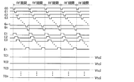
- the normal drive mode as shown in FIG. 2, the scanning signal lines G0 to G1 are sequentially selected in one frame period, and the image is displayed on the display unit 11 (of the pixel circuits Pix (1, 1) to Pix (n, m)).
- a refresh period for writing data hereinafter also referred to as an “RF period”
- a refresh period for writing data hereinafter also referred to as an “RF period”
- a non-refresh period (hereinafter also referred to as an “NRF” period) in which writing of image data to the display unit 11 is stopped is alternately repeated.
- NEF non-refresh period
- the scanning-side and data-side driving circuits are stopped in the non-refresh period, and the display by the image data written in the immediately preceding refresh period is continued. Therefore, the pause drive mode is effective in reducing the power consumption of the display device when displaying a still image.
- the external input signal Sin includes the operation mode signal Sm indicating which of the normal drive mode and the pause drive mode is used to drive the display unit 11 as described above.
- the operation mode signal Sm is supplied to the scanning drive circuit 40 as a part of the scanning control signal Scs, and is also supplied to the data drive circuit 30 as a part of the data control signal Scd.
- the scanning side drive circuit 40 drives the scanning signal lines G0 to Gn and the light emission control lines E1 to En according to the operation mode indicated by the operation mode signal Sm, and the data side drive circuit 30 uses the operation mode signal Sm.
- Data signal lines D1 to Dn are driven according to the indicated operation mode.
- the display control circuit 20 (the threshold control circuit 22) drives the threshold control lines TC1 to TCn according to the operation mode indicated by the operation mode signal Sm.
- a data write operation is performed when the corresponding scanning signal line Gi is in the selected state, and the scanning signal line Gi- immediately before the scanning signal line Gi is performed.
- the reset operation is performed, and the light emission control line Ei is driven so that each pixel circuit Pix (i, j) is in a non-light emitting state during a period in which the data write operation and the reset operation are performed.
- (I 1 to N). That is, as shown in FIGS. 2 and 3, in the RF period, the light emission control lines E1 to En are sequentially activated in two horizontal periods so as to be interlocked with the driving of the scanning signal lines G0 to Gn.
- each light emission control line Ei is , Is activated when a low level (L level) voltage is applied, and is deactivated when a high level (H level) voltage is applied.
- each threshold control line TCi is maintained at a predetermined threshold control initial voltage VtcI, and the threshold value of the drive transistor in each pixel circuit Pix (i, j) is Does not change (details will be described later).
- each threshold control line TCi gradually increases with time in the NRF period (non-refresh period), and the threshold voltage in the next RF period (refresh period). The voltage drops to the control initial voltage VtcI.
- each of the scanning signal lines G0 to Gn is maintained in a non-selected state (H level), and each of the light emission control lines E1 to En is maintained in an active state (L level). Therefore, during the NRF period, the scanning-side and data-side driving circuits are stopped, and each pixel circuit Pix (i, j) continues to emit light according to the data voltage held therein.
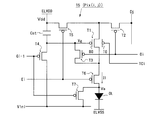
- FIG. 4 is a circuit diagram showing the configuration of the pixel circuit 15 in the present embodiment. More specifically, the pixel circuit 15 corresponding to the i-th scanning signal line Gi and the j-th data signal line Dj, that is, the i-th row and j-th column
- FIG. 3 is a circuit diagram illustrating a configuration of a pixel circuit Pix (i, j) (1 ⁇ i ⁇ n, 1 ⁇ j ⁇ m). As shown in FIG.
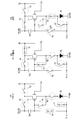
- the pixel circuit 15 includes an organic EL element OL as a display element, a drive transistor T1, a write control transistor T2, a threshold compensation transistor T3, a first initialization transistor T4, a first light emission control transistor T5, 2 includes a light emission control transistor T6, a second initialization transistor T7, and a holding capacitor Cst.
- the transistors T2 to T7 other than the driving transistor T1 function as switching elements.
- the pixel circuit 15 includes scanning signal lines Gi corresponding thereto (hereinafter also referred to as “corresponding scanning signal lines” in the description focusing on the pixel circuits), and scanning signal lines immediately before the corresponding scanning signal lines Gi (scanning signal lines G1 to G1).
- Gn is the immediately preceding scanning signal line in the scanning order, and is hereinafter also referred to as “preceding scanning signal line” in the description focusing on the pixel circuit.
- Gi-1 and the corresponding emission control line hereinafter, focusing on the pixel circuit).
- a corresponding light emission control line) Ei a corresponding threshold control line (hereinafter, also referred to as a “corresponding threshold control line” in the description focusing on the pixel circuit) TCi, and a corresponding data signal line (hereinafter, pixel circuit) , Dj, the initialization voltage supply line Vini, the high-level power supply line ELVDD, and the low-level power supply line ELV. S is connected.
- a corresponding threshold control line hereinafter, also referred to as a “corresponding threshold control line” in the description focusing on the pixel circuit” TCi
- a corresponding data signal line hereinafter, pixel circuit
- the source terminal of the drive transistor T1 is connected to the corresponding data signal line Dj via the write control transistor T2 and at the high level via the first light emission control transistor T5. It is connected to the power supply line ELVDD.
- the drain terminal of the driving transistor T1 is connected to the anode electrode of the organic EL element OL via the second emission control transistor T6.
- the gate terminal of the driving transistor T1 is connected to the high-level power supply line ELVDD via the holding capacitor Cst, is connected to the drain terminal of the driving transistor T1 via the threshold compensation transistor T3, and is connected to the first initialization transistor. It is connected to the initialization voltage supply line Vini via T4.
- the anode electrode of the organic EL element OL is connected to the initialization voltage supply line Vini via the second initialization transistor T7, and the cathode electrode of the organic EL element OL is connected to the low-level power supply line ELVSS.
- the gate terminals of the write control transistor T2 and the threshold compensation transistor T3 are connected to the corresponding scanning signal line Gi, and the gate terminals of the first and second light emission control transistors T5 and T6 are connected to the corresponding light emission control line Ei.
- Gate terminals of the first initialization transistor T4 and the second initialization transistor T7 are connected to the preceding scanning signal line Gi-1.
- the drive transistor T1 of the pixel circuit 15 in the present embodiment is a thin film transistor having a top gate electrode TG and a bottom gate electrode BG (details will be described later).
- the gate terminal of the second initialization transistor T7 may be connected to the corresponding scanning signal line Gi instead of the preceding scanning signal line Gi-1.
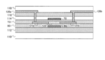
- FIG. 5 is a cross-sectional view showing one configuration example of the driving transistor T1.
- a bottom gate electrode BG is formed on an inorganic insulating film 112 as a moisture-proof layer formed on an insulating substrate 110 of a flexible substrate formed of a glass substrate or a resin material such as polyimide.
- a gate insulating film BGI is formed so as to cover it.
- a semiconductor layer is formed on the gate insulating film BGI.
- the semiconductor layer is formed of an intrinsic semiconductor 122 as a channel region, a conductor 121a as a source region and a drain region formed so as to face each other via the channel region. And the conductor 121b.
- a gate insulating film TGI is further formed on the semiconductor layer having such a configuration, and a top gate electrode TG is formed thereon.
- a first inorganic insulating film 114 and a second inorganic insulating film 116 are sequentially formed so as to cover the top gate electrode TG, and metal layers 120a and 120b for electrical connection with other elements are formed thereon. I have.
- the conductor 121a as a source region is electrically connected to the metal layer 120a through a contact hole
- the conductor 121b as a drain region is electrically connected to the metal layer 120b through a contact hole.
- an insulating layer 118 as a flattening film is formed so as to cover the metal layers 120a and 120b.
- the drive transistor T1 includes the top gate electrode TG arranged so as to face one surface (the upper surface in the drawing) of the channel region (intrinsic semiconductor layer) 122 via the gate insulating film TGI, and the channel region 122. And a bottom gate electrode BG disposed so as to face the other surface via the gate insulating film BGI (see FIG. 5).
- a double gate type such a configuration in which the gate electrode is provided on one surface side and the other surface side of the channel region.
- one of the two gate electrodes is used as an original control terminal (a terminal for controlling the current flowing through the transistor), and the other gate electrode is used by a voltage applied thereto.
- the bottom gate electrode BG is used as a main gate terminal (also referred to as a “main control terminal”) for controlling the current between the source and the drain.
- the top gate electrode TG is used as a threshold control terminal for controlling the threshold of the driving transistor T1.
- the bottom gate electrode BG as the main gate terminal is connected to the holding capacitor Cst, and the top gate electrode TG as the threshold control terminal is connected to the corresponding threshold control line TCi.
- the term “gate terminal” will simply refer to the “main gate terminal”.
- the drive transistor T1 operates in the saturation region, and the drive current I1 flowing through the organic EL element OL during the light emission period is given by the following equation (1).
- the gain ⁇ of the driving transistor T1 included in the equation (1) is given by the following equation (2).
- I1 ( ⁇ / 2) (
- ) 2 ( ⁇ / 2) (
- ⁇ ⁇ ⁇ (W / L) ⁇ Cox (2)
- Vgs, Vth, ⁇ , W, L, and Cox are the gate-source voltage, threshold value, mobility, gate width, and gate length of the driving transistor T1, respectively.
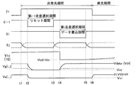
- FIG. 6 is a signal waveform diagram for explaining the operation of the pixel circuit in the present embodiment.
- FIG. 7A is a circuit diagram illustrating a reset operation of the pixel circuit 15 according to the present embodiment
- FIG. 7B is a circuit diagram illustrating a data write operation of the pixel circuit 15.
- 3C is a circuit diagram illustrating a lighting operation of the pixel circuit 15.
- FIG. 6 shows each signal line (correspondence) in the reset operation, the data write operation, and the lighting operation of the pixel circuit 15 of FIG. 4 configured as described above, that is, the pixel circuit Pix (i, j) of the i-th row and the j-th column.
- Vg and the voltage Va of the anode electrode of the organic EL element OL hereinafter referred to as “anode voltage”.
- a period from time t1 to t6 is a non-light emitting period of the pixel circuits Pix (i, 1) to Pix (i, m) in the i-th row.
- the period from time t2 to t4 is the (i-1) th horizontal period
- the period from time t2 to t3 is the selection period of the (i-1) th scanning signal line (preceding scanning signal line) Gi-1, that is, the (i-1) th scanning selection.
- the (i-1) th scanning selection period corresponds to a reset period of the pixel circuits Pix (i, 1) to Pix (i, m) on the i-th row.
- the period from time t4 to t6 is the i-th horizontal period, and the period from time t4 to t5 is the selection period of the i-th scanning signal line (corresponding scanning signal line) Gi, that is, the i-th scanning selection period.
- the i-th scanning selection period corresponds to a data writing period of the pixel circuits Pix (i, 1) to Pix (i, m) on the i-th row.
- the first initialization transistor T4 changes to the ON state.
- the voltage of the main gate terminal of the driving transistor T1 that is, the gate voltage Vg
- the initialization voltage Vini is a voltage that can keep the drive transistor T1 in the ON state when a data voltage is written to the pixel circuit Pix (i, j).
- the second initialization transistor T7 also changes to the ON state.
- the accumulated charge in the parasitic capacitance of the organic EL element OL is discharged, and the anode voltage Va of the organic EL element is initialized to the initialization voltage Vini (see FIG. 6).
- the symbol “Va (i, j)” is used to distinguish the anode voltage Va in the pixel circuit Pix (i, j) from the anode voltage Va in other pixel circuits (the same applies to the following).
- the voltage of the corresponding threshold control line TCi is initialized to a predetermined threshold control initial voltage VtcI, and thereafter, in the next frame period, the preceding scanning signal line Gi-1 is in the selected state. (Until the start of the (i-1) th selective scanning period in the next frame period).
- the period from time t2 to time t3 is a reset period in the pixel circuits Pix (i, 1) to Pix (i, m) in the i-th row.
- the reset period is as described above.
- the first initialization transistor T4 is in the ON state.
- FIG. 7A schematically shows the state of the pixel circuit Pix (i, j) during the reset period, that is, the circuit state during the reset operation.
- a dotted circle indicates that a transistor as a switching element therein is in an off state
- a dotted rectangle indicates that a transistor as a switching element therein is in an on state. (This expression method is also employed in FIGS. 7B and 7C).
- FIG. 6 shows a change in the gate voltage Vg (i, j) in the pixel circuit Pix (i, j) at this time. Note that the symbol “Vg (i, j)” is used to distinguish the gate voltage Vg in the pixel circuit Pix (i, j) from the gate voltage Vg in other pixel circuits (the same applies to the following).
- the data-side driving circuit 30 supplies the data signal D (j) as the data voltage of the pixel in the i-th row and the j-th column to the data signal line Dj.
- the application is started, and the application of the data signal D (j) is continued at least until the end time t5 of the i-th scanning selection period.
- the voltage of the corresponding scanning signal line Gi changes from the H level to the L level, so that the corresponding scanning signal line Gi is in the selected state. Therefore, in the pixel circuit Pix (i, j), the write control transistor T2 and the threshold compensation transistor T3 change to the ON state.
- the period from time t4 to time t5 is a data writing period in the pixel circuits Pix (i, 1) to Pix (i, m) on the i-th row.
- the write control transistor T2 and the threshold compensation transistor T3 are on.
- FIG. 7B schematically shows the state of the pixel circuit Pix (i, j) during the data writing period, that is, the circuit state during the data writing operation.
- the voltage of the corresponding data signal line Dj is applied as the data voltage Vdata to the holding capacitor Cst via the diode-connected drive transistor T1.
- the gate voltage Vg (i, j) changes toward the value given by the following equation (5).
- Vg (i, j) Vdata ⁇
- FIG. 7C schematically shows the state of the pixel circuit Pix (i, j) during the light emission period, that is, the circuit state during the lighting operation.
- the high level power supply line ELVDD is connected to the low level power supply line ELVSS via the first light emission control transistor T5, the driving transistor T1, the second light emission control transistor T6, and the organic EL element OL.
- the current I1 flows.
- This current I1 is given by the above equation (1).
- the drive transistor T1 is of a P-channel type and ELVDD> Vg, from the above equations (1) and (5), this current I1 is given by the following equation.
- each pixel circuit Means that the organic EL element is not turned on not only during the data writing period (i-th scan selection period shown in FIG. 6) but also during the previous reset period (i-1-th scan selection period shown in FIG. 6). , And is in a non-light emitting state for at least both periods.
- the threshold Vth of the drive transistor T1 of each pixel circuit Pix (i, j) is set to the threshold control line TCi given to its threshold control terminal (top gate electrode) TG. It is controlled by the voltage, that is, the voltage of the threshold control signal TC (i) (hereinafter referred to as “threshold control voltage”) Vtc (i) (see FIGS. 3 and 6).
- threshold control voltage the voltage of the threshold control signal TC (i) (hereinafter referred to as “threshold control voltage”) Vtc (i) (see FIGS. 3 and 6).
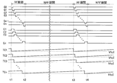
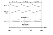
- a long NRF period is provided between two adjacent RF periods as shown in FIG. 3, so that a writing cycle (refresh cycle) of a data voltage to the pixel circuit Pix (i, j) is normally performed. It is much longer than the drive mode, for example, about 0.1 second or more (refresh rate is 10 Hz or less). Therefore, in the light emitting period including the NRF period, the amount of change in the charge stored in the holding capacitor Cst due to the leakage current Ioff of the first initialization transistor T4 in the off state increases. As a result, the amount of decrease in the gate voltage Vg (i, j) of the drive transistor T1 in one refresh cycle Tref-PD in the idle drive mode also increases.
- the gate voltage Vg (i, j) thus reduced rises by writing a new data voltage in the next RF period (time Tw1 to Tw4 shown in FIG. 8 indicate the time of this writing). Therefore, in the idle drive mode, the gate voltage Vg (i, j) of the drive transistor T1 periodically changes in the refresh cycle Tref-PD as shown in FIG. In response, the luminance L (i, j) of the organic EL element OL in the pixel circuit Pix (i, j) gradually increases as shown in FIG. 8, and this is visually recognized as flicker.
- the threshold control line TCi is driven to change as shown.
- of the threshold value of the driving transistor T1 gradually increases in the light emission period including the NRF period, and the start time t2 of the (i-1) th selective scanning period in the next RF period (this time is 9 at substantially the same time as the data writing times Tw1 to Tw4), the threshold control initial voltage VtcI drops.
- the threshold control voltage Vtc (i) applied to the threshold control terminal TG of the drive transistor T1 periodically changes at the refresh cycle Tref-PD as shown in FIG.
- of the threshold value of the drive transistor T1 increases as the voltage Vtc (i) applied to the threshold control terminal TG increases in the positive direction (the current increases). It becomes difficult to flow).
- acts in the direction of decreasing the drive current I1 of the organic EL element OL by the drive transistor T1 to lower the luminance. Therefore, by appropriately setting the rate of change of the threshold control voltage Vtc (i) during the light emitting period according to the characteristics of the driving transistor T1, the luminance L (i, j) of the organic EL element OL in the pixel circuit Pix (i, j) is obtained.
- the change in j) can be reduced as shown by the solid line in FIG. Therefore, in the idle drive mode, it is possible to suppress the occurrence of flicker due to the change in the amount of charge stored in the holding capacitor Cst due to the leakage current of the first initialization transistor T4.
- the drive current I1 flowing from the drive transistor T1 to the organic EL element OL during the light emission period is given by the above-described equation (1).
- Vdd ELVDD
- Vg Vg (i, j) changes due to the leakage current Ioff of the first initialization transistor T4 during the light emission period
- this gate voltage Vg is regarded as a function of the time t and is set to Vg (t).
- Vg (0) Vdata-
- the gate voltage Vg (t) that changes due to the leakage current Ioff of the first initialization transistor T4 that is in the off state during the light emission period can be expressed by the following equation from FIGS. 4 and 7C.
- Vg (t) (Vg (0) ⁇ Vini) exp ( ⁇ t / (Cst ⁇ Roff)) + Vini (9)
- Vini indicates the initialization voltage
- Cst indicates the capacitance value of the holding capacitor Cst
- Roff indicates the off-resistance of the first initialization transistor T4.
- the voltage gradually decreases from Vg (0) shown in the above equation (8), and rises to Vg (0) shown in the above (8) by writing the data voltage in the next RF period. That is, the gate voltage Vg periodically changes in the refresh cycle Tref-PD in the pause drive mode as shown in FIG.
- the driving current I1 is increased in the light emitting period after the data writing period according to the above equations (8) and (10).
- I1 ( ⁇ / 2) (Vdd ⁇ Vg (0) ⁇
- ) 2 ( ⁇ / 2) (Vdd ⁇ Vdata) 2
- I1 ( ⁇ / 2) (Vdd ⁇ Vdata) 2
- the luminance L (i, j) of the organic EL element OL of the current drive type periodically changes in the refresh cycle Tref-PD in the pause drive mode as shown in FIG.
- Such a change in the luminance L (i, j) of the organic EL element OL is visually recognized as flicker.
- the threshold control terminal (top gate electrode) TG of the drive transistor T1 is connected to the threshold control voltage Vtc (i) via the threshold control line TCi. To control the threshold value Vth of the driving transistor T1.
- this threshold is regarded as a function Vth (t) of the time t, and ideally Vg (t) +
- Vg (0) +
- the threshold Vth (t) may be controlled so that By doing so, the driving current I1 does not change and the value shown by the following equation is maintained from the equation (10).
- I1 ( ⁇ / 2) (Vdd ⁇ Vg (0) ⁇
- Vg (t) represented by the above equation (9) is approximated by the following equation.
- Vg (t) (Vg (0) ⁇ Vini) (1 ⁇ t / (Cst ⁇ Roff)) + Vini (13) From the above equations (11) and (13),
- can be expressed by the following linear expression with respect to the voltage Vtg of the top gate electrode TG. it can.
- a ⁇ Vtg + b
- the threshold control voltage Vtc (i) given as Vtg is given to the top gate electrode TG, the above equation can be rewritten as follows.
- Vtc (i, t) ⁇
- ⁇ b ⁇ / a ⁇
- the threshold control voltage Vtc (i) that changes according to the above equation (17) is changed to the threshold control line TCi.
- the threshold control signals TC (1) to TC (n) are provided by the threshold control circuit 22. It is generated and applied to the threshold control lines TC1 to TCn (see FIGS. 9 and 3).
- the threshold control voltage Vtc (i, t) represented by the above equation (17) corresponds to the voltage of the threshold control signal TC (i).
- the control voltage Vtc (i, t) may be generated.
- the data voltage representative value Vdpr for the data voltage to be written to the corresponding pixel circuits Pix (i, 1) to Pix (i, m) is determined.
- the threshold control voltage Vtc (i) to be applied to the threshold control terminal TG of the drive transistor T1 in the pixel circuits Pix (i, 1) to Pix (i, m) corresponding to the threshold control line TCi is represented by the data voltage representative value Vdpr.
- Vtc (i, t) VtcI + (Vdpr ⁇
- the data voltage indicating the lowest luminance among the n ⁇ m data voltages Vdata may be determined as the data voltage representative value Vdrp.
- a predetermined value based on various display images may be set as the data voltage representative value Vdpr for the n ⁇ m data voltages Vdata.
- the same data voltage representative value Vdpr is determined for each threshold value control line TCi, so that the display control circuit 20 drives all the pixel circuits Pix (1,1) to Pix (n, m).
- threshold control voltage represented by the same time function Vtc (t) is applied to all the pixel circuits Pix (1,1) to Pix (n, m) as shown above, as shown in FIG.
- n threshold control lines TC1 to TCn arranged along the scanning signal lines G1 to Gn
- m threshold control lines TC1 to TCm are arranged along the data signal lines D1 to Dm. Is also good.
- the threshold control voltage represented by the same time function Vtc (t) is given to all the pixel circuits Pix (1,1) to Pix (n, m) as described above, the threshold to be provided
- the control lines do not necessarily need to correspond one-to-one with the scanning signal lines G1 to Gn or the data signal lines D1 to Dm. Therefore, the number of threshold control lines is The number may be less than the number of lines D1 to Dm.
- the threshold control voltage Vtc (i) that changes in the direction to the threshold control terminal TG
- the change in the gate voltage Vg is compensated.
- an increase in drive current due to a decrease in the gate voltage Vg is suppressed, and the occurrence of flicker due to a change in luminance of the organic EL element OL in the refresh cycle Tref-PD can be prevented. Therefore, in the pause drive mode, it is possible to display a good image in which flicker is not visually recognized while reducing power consumption.
- FIG. 10 is a block diagram illustrating an overall configuration of an organic EL display device 10b according to the second embodiment.
- the display device 10b according to the present embodiment is also an organic EL display device that performs internal compensation.
- the display device 10b also includes a display unit 11b, a display control circuit 20, a data drive circuit 30, a scan drive circuit 40b, and a power supply circuit 50, as in the first embodiment.
- the display unit 11b is different from the first embodiment in that the threshold control lines TC1 to TCn are not provided.
- the display control circuit 20 of the present embodiment does not include a threshold control circuit.
- Other points in the overall configuration of the present embodiment are the same as those in the first embodiment (see FIG. 1), and the same or corresponding parts are denoted by the same reference characters and description thereof is omitted.
- the display device 10b also has two operation modes, a normal drive mode and a pause drive mode, as in the first embodiment. Also, as in the first embodiment, in the normal drive mode, the refresh period (RF period) is repeated as shown in FIG. 2, whereas in the pause drive mode, the refresh period (RF period) as shown in FIG. ) And the non-refresh period (NRF period) are alternately repeated.
- the voltage Vtc for controlling the threshold value Vth of the driving transistor is generated in each pixel circuit (details will be described later).
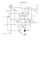
- FIG. 11 is a circuit diagram illustrating a configuration of the pixel circuit 15b according to the present embodiment. More specifically, the pixel circuit 15b corresponding to the i-th scanning signal line Gi and the j-th data signal line Dj, that is, the i-th row and j-th column
- FIG. 3 is a circuit diagram illustrating a configuration of a pixel circuit Pix (i, j) (1 ⁇ i ⁇ n, 1 ⁇ j ⁇ m).
- the pixel circuit 15b has an organic EL element OL as a display element, a drive transistor T1, a write control transistor T2, and a threshold, similarly to the pixel circuit 15 in the first embodiment (FIG. 4).
- the pixel circuit 15b includes a threshold control transistor T8, a threshold control capacitor Ctc, and a threshold control resistance element Rtc.
- the resistance value of the threshold control resistance element Rtc is sufficiently larger than the ON resistance of the threshold control transistor T8.
- the resistance value is smaller than the off resistance of the threshold control transistor T8 (in the present embodiment, the resistance value is sufficiently smaller than the off resistance of the threshold control transistor T8).
- Such a threshold control resistance element Rtc can be realized using a conductor region in a semiconductor layer formed on the gate insulating film BGI as shown in FIG. 5, for example, and can be realized using a transistor. Can also. In the latter case, for example, as shown in FIG. 13, a P-channel transistor T9 whose on-resistance is larger than usual by reducing the channel width W and increasing the channel length is used, and the light emission control corresponding to the gate terminal is performed. By connecting the line Ei, the threshold control resistance element Rtc can be realized.
- the transistors T2 to T8 other than the driving transistor T1 function as switching elements.
- the drive transistor T1 is a double-gate P-channel transistor having a top gate electrode TG and a bottom gate electrode BG (see FIG. 5), and the bottom gate electrode BG is The top gate electrode TG is used as a threshold control terminal for controlling the threshold value of the drive transistor T1, which is used as a main gate terminal for controlling the current flowing through the drive transistor T1.
- the pixel circuit 15b includes a corresponding scanning signal line Gi corresponding to the corresponding scanning signal line, a preceding scanning signal line Gi-1 corresponding to a scanning signal line immediately before the corresponding scanning signal line Gi, and a corresponding light emission control line.
- the corresponding light emission control line Ei, the corresponding data signal line Dj corresponding thereto, the initialization voltage supply line Vini, the high-level power line ELVDD, and the low-level power line ELVSS are connected.
- these signal lines, power supply lines and the like and elements other than the threshold control transistor T8, the threshold control capacitor Ctc, and the threshold control resistance element Rtc (organic EL element OL, drive transistor T1, write control transistor T2, threshold
- the connection form between the threshold control capacitor Ctc and the element other than the threshold control resistance element is the same as that of the pixel circuit 15 in the first embodiment (see FIGS. 4 and 11).
- the pixel circuit 15b includes a threshold control transistor T8, a threshold control capacitor Ctc, and a threshold control resistance element Rtc, unlike the first embodiment, and includes a drive transistor T1. Is connected to the high-level power supply line ELVDD via the threshold control capacitor Ctc, and to the initialization voltage supply line Vini via the threshold control transistor T8. It is connected to the high-level power supply line ELVDD via the control resistance element Rtc.
- FIG. 12 is a signal waveform diagram for explaining the operation of the pixel circuit 15b according to the present embodiment.
- the pixel circuit 15b of FIG. 11 configured as described above, that is, the pixel circuit Pix (i, i, Each signal line (corresponding light emission control line Ei, preceding scanning signal line Gi-1, corresponding scanning signal line Gi, corresponding data signal line Dj, threshold control terminal TG) in the reset operation, data writing operation, and lighting operation of j).
- the voltage (gate voltage) Vg of the main gate terminal of the drive transistor T1 The voltage (anode voltage) Va of the anode electrode of the organic EL element OL.
- each signal line (corresponding light emission control line Ei, preceding scanning signal) connected to each pixel circuit Pix (i, j)
- the line Gi-1, the corresponding scanning signal line Gi, and the corresponding data signal line Dj) are driven in the same manner as in the first embodiment, and the pixel circuit Pix (i, j) in the present embodiment also operates in the first embodiment.
- the same reset operation, data write operation, and lighting operation as in the embodiment are performed.
- the voltage applied to the threshold control terminal TG of the drive transistor T1 of each pixel circuit Pix (i, j) is applied from the threshold control circuit in the display control circuit 20 via the corresponding threshold control line TCi. Instead, it is generated using the threshold control transistor T8, the threshold control capacitor Ctc, and the threshold control resistance element Rtc in the pixel circuit Pix (i, j). The details will be described below.
- the voltage (hereinafter, referred to as “threshold control voltage”) Vtc of the threshold control terminal TG of the drive transistor T1 changes as shown in FIG. That is, since the corresponding scanning signal line Gi is connected to the gate terminal of the threshold control transistor T8, as shown in FIG. 12, the threshold control transistor T8 is turned off at the start time t4 of the data writing period corresponding to the i-th scanning selection period. To the on state, and is maintained in the on state until the end point t5 of the data writing period.
- the threshold control capacitor Ctc is charged by the high-level power supply line ELVDD and the initialization voltage supply line Vini to hold the voltage Vdd-Vini. Thereafter, the threshold control transistor T8 is turned off at the end time t5 of the data writing period, and thereafter, while the threshold control transistor T8 is in the off state, the charge accumulated in the threshold control capacitor Ctc passes through the threshold control resistor Rtc. Is discharged. Therefore, the threshold control voltage Vtc (t) at this time can be expressed by the following equation.
- Vtc (t) (Vini ⁇ Vdd) exp ( ⁇ t / (Ctc ⁇ Rtc)) + Vdd (19)
- Vtc (t) expressed by the above equation (19) is approximated by the following equation.
- the threshold control capacitor is set so as to satisfy the following equation. It can be seen that it is sufficient to set the capacitance value of Ctc (also denoted by reference numeral “Ctc”) and the resistance value of the threshold control resistance element Rtc (also denoted by reference numeral “Rtc”).
- the capacitance value Ctc of the threshold control capacitor and the resistance value Rtc of the threshold control resistance element may be set according to (20). However, since the capacitance value Ctc and the resistance value Rtc are circuit constants, the data voltage representative value Vdpr determined in the present embodiment is a fixed value.
- the threshold for generating the threshold control voltage Vtc using the threshold control capacitor Ctc, the threshold control transistor T8, and the threshold control resistor Rtc is configured (see FIG. 11), and the threshold Vth of the drive transistor T1 is controlled by the threshold control voltage Vtc.
- the same effect as in the first embodiment can be obtained without generating .about.Vtc (n) (see FIG. 9).
- the threshold control voltage Vtc (i) is fixed at VtcI in the normal drive mode, but the threshold control voltage Vtc (i) may be changed similarly to the pause drive mode (FIG. 3, see FIG. 9).
- the pixel circuits Pix (i, 1) to P (i, m) of each row change at timings corresponding to the row by the threshold control lines TC1 to TCn.
- the threshold control voltage Vtc (i) is given to the threshold control terminal TG of the drive transistor T1 in the pixel circuits Pix (i, 1) to P (i, m) of the row (see FIG. 3).
- the threshold control signals TC (1) to TC (n) to be applied to the threshold control lines TC1 to TCn, respectively have the same voltage (the same value). May be generated.
- the n threshold control lines TC1 to TCn are shared by one threshold control line, and the threshold control voltage Vtc as the same time function is applied to all the pixel circuits Pix (1, 1) to P (n, m) may be applied to the threshold control terminal TG of the drive transistor T1.
- the top gate electrode TG of the drive transistor T1 is used as a threshold control terminal
- the bottom gate electrode BG is a main gate terminal (a control terminal for controlling a current flowing through the drive transistor T1).
- the top gate electrode TG may be used as a main gate terminal
- the bottom gate electrode BG may be used as a threshold control terminal.
- the point in time when the voltage returns to the threshold control initial voltage VtcI (Vini) is, as shown in FIG. This is the start time t2 of the (i-1 scan selection period), and in the second embodiment, as shown in FIG. 12, the start of the data writing period (i-th scan selection period) in the pixel circuit Pix (i, j). It is time t4.
- the point in time when the threshold control voltage Vct (t) returns to the threshold control initial voltage VtcI (Vini) is within the non-emission period (preferably in the period t1 to t4 before the start time t4 of the data writing period).
- the corresponding scanning signal line Gi is connected to the gate terminal of the threshold value control transistor T8 in the pixel circuit Pix (i, j).
- the preceding scanning signal line Gi-1 may be connected to the gate terminal.
- the pixel circuits 15 and 15b of the internal compensation system as shown in FIGS. 4 and 11, respectively, are used, but the configuration of the pixel circuit is limited to these configurations. Not something. That is, the driving transistor controls a driving current of a current-driven display element such as an organic EL element according to a voltage held in the holding capacitor.
- the present invention can be applied to any configuration in which the holding voltage may change.
- a P-channel transistor is used as the driving transistor T1 in the pixel circuits 15 and 15b (see FIGS. 4 and 11), but an N-channel transistor is used for the driving transistor T1 and the like.
- Type transistor eg, In—Ga—Zn—O (indium gallium zinc oxide) which is an oxide semiconductor containing indium (In), gallium (Ga), zinc (Zn), and oxygen (O) as main components.
- the present invention can be applied even when an N-channel thin film transistor having a channel layer formed thereon is used, and the same effect is obtained by applying the present invention (flicker does not occur even when pause driving is performed). An effect that good display can be performed) can be obtained.
- the leakage current of the first initialization transistor T4 is considered as a factor of the decrease in the gate voltage Vg (the holding voltage of the holding capacitor Cst) that causes flicker in a display image, and the gate voltage is reduced.
- the formula of the threshold control voltage Vtc for compensating the decrease by formulating the decrease of Vg is derived.
- a leakage current due to another path for example, from the main gate terminal of the driving transistor T1 to the low-level power line ELVSS via the threshold compensation transistor T3, the light emission control transistor T6, and the organic EL element OL. Even when the leakage current due to the leading path cannot be ignored, it is possible to formulate a decrease in the gate voltage Vg and derive a mathematical expression of the threshold control voltage Vtc for compensating the decrease in the same way as described above.
- the embodiments and the modified examples have been described by taking the organic EL display device as an example.
- the present invention is not limited to the organic EL display device, and uses a display element driven by current. Any applicable display device is applicable.
- the display element that can be used here is a display element whose luminance or transmittance or the like is controlled by current.
- an organic EL element that is, an organic light emitting diode (Organic Light Emitting Diode (OLED)), an inorganic light emitting diode, Quantum dot light emitting diodes (Quantum dot light emitting diode (QLED)) and the like can be used.
- OLED Organic Light Emitting Diode
- QLED Quantum dot light emitting diodes
- Vini initialization voltage supply line, initialization voltage
- ELVDD high-level power supply line (first power supply line), high-level power supply voltage
- ELVSS low-level power supply line (second power supply line)
- OLED organic EL element (Display element)
- Ctc Threshold control capacitor
- Rtc Threshold control resistor element
- T4 First initialization transistor (initial switching element)
- T5 First light emission control transistor
- T6 Second light emission control transistor
Abstract
La présente invention concerne un dispositif d'affichage de type à courant électrique d'attaque qui peut réaliser un bon affichage sans générer de papillotement même lorsqu'un arrêt de l'attaque est effectué. Dans un circuit de pixels (15), après initialisation d'une tension de grille (Vg) par un premier transistor d'initialisation (T4), une tension d'une ligne de signal de données (Di) est écrite sur un condensateur de maintien (Cst) par l'intermédiaire d'un transistor de commande d'écriture (T2) et d'un transistor d'attaque (T1). Ensuite, des transistors de commande d'émission de lumière (T5), (T6) sont activés, et un élément EL organique (OL) émet de la lumière lors de la réception d'un courant électrique d'attaque (I1) provenant du transistor d'attaque (T1). Dans la période de cette émission de lumière, même lorsque la tension de grille (Vg) est diminuée par un courant électrique de fuite du premier transistor d'initialisation (T4) dans un état ARRÊT, une compensation de la diminution est effectuée par augmentation d'une tension de commande de valeur seuil à appliquer à une borne de commande de valeur seuil (TG) du transistor d'attaque (T1). Par conséquent, même lorsqu'un cycle de rafraîchissement devient long en raison d'un arrêt de l'attaque, une augmentation de luminosité provoquée par une diminution de la tension de grille (Vg) peut être supprimée, et la génération de papillotement peut être empêchée.
Priority Applications (3)
| Application Number | Priority Date | Filing Date | Title |
|---|---|---|---|
| PCT/JP2018/036597 WO2020066024A1 (fr) | 2018-09-28 | 2018-09-28 | Dispositif d'affichage et son procédé d'attaque |
| US17/280,124 US11557251B2 (en) | 2018-09-28 | 2018-09-28 | Display device and drive method therefor |
| CN201880098066.5A CN112771603B (zh) | 2018-09-28 | 2018-09-28 | 显示装置及其驱动方法 |
Applications Claiming Priority (1)
| Application Number | Priority Date | Filing Date | Title |
|---|---|---|---|
| PCT/JP2018/036597 WO2020066024A1 (fr) | 2018-09-28 | 2018-09-28 | Dispositif d'affichage et son procédé d'attaque |
Publications (1)
| Publication Number | Publication Date |
|---|---|
| WO2020066024A1 true WO2020066024A1 (fr) | 2020-04-02 |
Family
ID=69951287
Family Applications (1)
| Application Number | Title | Priority Date | Filing Date |
|---|---|---|---|
| PCT/JP2018/036597 WO2020066024A1 (fr) | 2018-09-28 | 2018-09-28 | Dispositif d'affichage et son procédé d'attaque |
Country Status (3)
| Country | Link |
|---|---|
| US (1) | US11557251B2 (fr) |
| CN (1) | CN112771603B (fr) |
| WO (1) | WO2020066024A1 (fr) |
Cited By (2)
| Publication number | Priority date | Publication date | Assignee | Title |
|---|---|---|---|---|
| CN114765007A (zh) * | 2021-01-04 | 2022-07-19 | 京东方科技集团股份有限公司 | 显示装置、像素电路及其驱动方法 |
| WO2023209943A1 (fr) * | 2022-04-28 | 2023-11-02 | シャープディスプレイテクノロジー株式会社 | Circuit de pixels, dispositif d'affichage et procédé d'attaque de dispositif d'affichage |
Families Citing this family (8)
| Publication number | Priority date | Publication date | Assignee | Title |
|---|---|---|---|---|
| US11551611B2 (en) * | 2018-12-18 | 2023-01-10 | Samsung Display Co., Ltd. | Pixel circuit and organic light emitting display device including i he same |
| KR20210081538A (ko) * | 2019-12-24 | 2021-07-02 | 엘지디스플레이 주식회사 | 유기 전계발광 표시장치 및 그의 구동방법 |
| CN111179851A (zh) * | 2020-02-25 | 2020-05-19 | 合肥鑫晟光电科技有限公司 | 像素电路及其驱动方法、和显示装置 |
| KR20220064624A (ko) * | 2020-11-12 | 2022-05-19 | 엘지디스플레이 주식회사 | 표시패널과 이를 이용한 표시장치 |
| CN113314073B (zh) * | 2021-05-17 | 2022-04-08 | 上海天马微电子有限公司 | 显示面板及显示装置 |
| CN115512631A (zh) * | 2021-06-22 | 2022-12-23 | 荣耀终端有限公司 | 像素驱动电路及其驱动方法、显示面板及终端设备 |
| CN114743500B (zh) * | 2022-04-25 | 2023-07-25 | 福建华佳彩有限公司 | 一种高解析度的5t2c ltpo内部补偿电路及其控制方法 |
| KR20240029669A (ko) * | 2022-08-26 | 2024-03-06 | 삼성디스플레이 주식회사 | 표시 장치 |
Citations (6)
| Publication number | Priority date | Publication date | Assignee | Title |
|---|---|---|---|---|
| JP2012014136A (ja) * | 2010-06-30 | 2012-01-19 | Samsung Mobile Display Co Ltd | 有機電界発光表示装置用画素及びこれを利用した有機電界発光表示装置 |
| JP2013003568A (ja) * | 2011-06-22 | 2013-01-07 | Sony Corp | 画素回路、表示装置、電子機器、及び、画素回路の駆動方法 |
| JP2015014763A (ja) * | 2013-07-08 | 2015-01-22 | ソニー株式会社 | 表示装置、表示装置の駆動方法、及び、電子機器 |
| WO2015037331A1 (fr) * | 2013-09-10 | 2015-03-19 | シャープ株式会社 | Dispositif d'affichage et son procédé de commande |
| US20180144685A1 (en) * | 2016-11-23 | 2018-05-24 | Lg Display Co., Ltd. | Display device and method of compensating for deterioration of the same |
| US20180158406A1 (en) * | 2016-12-05 | 2018-06-07 | Samsung Display Co., Ltd. | Display device and method for driving the same |
Family Cites Families (22)
| Publication number | Priority date | Publication date | Assignee | Title |
|---|---|---|---|---|
| JP4638117B2 (ja) * | 2002-08-22 | 2011-02-23 | シャープ株式会社 | 表示装置およびその駆動方法 |
| TWI253614B (en) * | 2003-06-20 | 2006-04-21 | Sanyo Electric Co | Display device |
| TWI330726B (en) * | 2005-09-05 | 2010-09-21 | Au Optronics Corp | Display apparatus, thin-film-transistor discharge method and electrical driving method therefor |
| JP2013003569A (ja) | 2011-06-22 | 2013-01-07 | Sony Corp | 画素回路、表示装置、電子機器、及び、画素回路の駆動方法 |
| CN102346999B (zh) * | 2011-06-27 | 2013-11-06 | 昆山工研院新型平板显示技术中心有限公司 | Amoled像素电路及其驱动方法 |
| JP5998458B2 (ja) * | 2011-11-15 | 2016-09-28 | セイコーエプソン株式会社 | 画素回路、電気光学装置、および電子機器 |
| US9786223B2 (en) * | 2012-12-11 | 2017-10-10 | Ignis Innovation Inc. | Pixel circuits for AMOLED displays |
| CN104575367B (zh) * | 2013-10-15 | 2017-10-13 | 昆山工研院新型平板显示技术中心有限公司 | 一种像素电路及其驱动方法和应用 |
| CN104715712B (zh) * | 2013-12-11 | 2018-05-25 | 昆山工研院新型平板显示技术中心有限公司 | 一种像素电路及其驱动方法和应用 |
| KR102190161B1 (ko) * | 2014-06-23 | 2020-12-14 | 삼성디스플레이 주식회사 | 화소, 표시 패널 및 이를 포함하는 유기 발광 표시 장치 |
| KR102241704B1 (ko) * | 2014-08-07 | 2021-04-20 | 삼성디스플레이 주식회사 | 화소 회로 및 이를 포함하는 유기 발광 표시 장치 |
| KR102221761B1 (ko) * | 2014-10-14 | 2021-03-03 | 삼성디스플레이 주식회사 | 화소, 이를 포함하는 표시 장치용 기판 및 표시 장치 |
| KR102288351B1 (ko) * | 2014-10-29 | 2021-08-11 | 삼성디스플레이 주식회사 | 표시장치 및 그 구동방법 |
| CN104464630B (zh) * | 2014-12-23 | 2018-07-20 | 昆山国显光电有限公司 | 像素电路及其驱动方法和有源矩阵有机发光显示器 |
| CN104658484B (zh) * | 2015-03-18 | 2018-01-16 | 上海和辉光电有限公司 | 显示装置、像素驱动电路及其驱动方法 |
| EP3098805B1 (fr) * | 2015-05-28 | 2018-07-25 | LG Display Co., Ltd. | Affichage électroluminescent organique et circuit correspondant |
| CN105139807B (zh) * | 2015-10-22 | 2019-01-04 | 京东方科技集团股份有限公司 | 一种像素驱动电路、显示装置及其驱动方法 |
| KR20170049735A (ko) | 2015-10-28 | 2017-05-11 | 삼성디스플레이 주식회사 | 표시 장치 |
| US10388219B2 (en) * | 2016-06-30 | 2019-08-20 | Lg Display Co., Ltd. | Organic light emitting display device and driving method of the same |
| CN106531074B (zh) * | 2017-01-10 | 2019-02-05 | 上海天马有机发光显示技术有限公司 | 有机发光像素驱动电路、驱动方法以及有机发光显示面板 |
| KR102344964B1 (ko) * | 2017-08-09 | 2021-12-29 | 엘지디스플레이 주식회사 | 표시장치, 전자기기 및 바디 바이어싱 회로 |
| KR102462008B1 (ko) * | 2017-09-22 | 2022-11-03 | 삼성디스플레이 주식회사 | 유기 발광 표시 장치 |
-
2018
- 2018-09-28 US US17/280,124 patent/US11557251B2/en active Active
- 2018-09-28 CN CN201880098066.5A patent/CN112771603B/zh active Active
- 2018-09-28 WO PCT/JP2018/036597 patent/WO2020066024A1/fr active Application Filing
Patent Citations (6)
| Publication number | Priority date | Publication date | Assignee | Title |
|---|---|---|---|---|
| JP2012014136A (ja) * | 2010-06-30 | 2012-01-19 | Samsung Mobile Display Co Ltd | 有機電界発光表示装置用画素及びこれを利用した有機電界発光表示装置 |
| JP2013003568A (ja) * | 2011-06-22 | 2013-01-07 | Sony Corp | 画素回路、表示装置、電子機器、及び、画素回路の駆動方法 |
| JP2015014763A (ja) * | 2013-07-08 | 2015-01-22 | ソニー株式会社 | 表示装置、表示装置の駆動方法、及び、電子機器 |
| WO2015037331A1 (fr) * | 2013-09-10 | 2015-03-19 | シャープ株式会社 | Dispositif d'affichage et son procédé de commande |
| US20180144685A1 (en) * | 2016-11-23 | 2018-05-24 | Lg Display Co., Ltd. | Display device and method of compensating for deterioration of the same |
| US20180158406A1 (en) * | 2016-12-05 | 2018-06-07 | Samsung Display Co., Ltd. | Display device and method for driving the same |
Cited By (3)
| Publication number | Priority date | Publication date | Assignee | Title |
|---|---|---|---|---|
| CN114765007A (zh) * | 2021-01-04 | 2022-07-19 | 京东方科技集团股份有限公司 | 显示装置、像素电路及其驱动方法 |
| US11587501B2 (en) | 2021-01-04 | 2023-02-21 | Boe Technology Group Co., Ltd. | Display apparatuses, pixel circuits and methods of driving pixel circuit |
| WO2023209943A1 (fr) * | 2022-04-28 | 2023-11-02 | シャープディスプレイテクノロジー株式会社 | Circuit de pixels, dispositif d'affichage et procédé d'attaque de dispositif d'affichage |
Also Published As
| Publication number | Publication date |
|---|---|
| US20210343238A1 (en) | 2021-11-04 |
| CN112771603B (zh) | 2023-07-11 |
| US11557251B2 (en) | 2023-01-17 |
| CN112771603A (zh) | 2021-05-07 |
Similar Documents
| Publication | Publication Date | Title |
|---|---|---|
| WO2020066024A1 (fr) | Dispositif d'affichage et son procédé d'attaque | |
| US11398187B2 (en) | Display device and method for driving same | |
| JP5176522B2 (ja) | 自発光型表示装置およびその駆動方法 | |
| JP5115180B2 (ja) | 自発光型表示装置およびその駆動方法 | |
| TWI436334B (zh) | 顯示器裝置 | |
| KR101174784B1 (ko) | 발광표시장치 | |
| JP2010008521A (ja) | 表示装置 | |
| CN111886644B (zh) | 显示装置及其驱动方法 | |
| US11189235B2 (en) | Display device and method for driving same | |
| US11120741B2 (en) | Display device and method for driving same | |
| CN114097022B (zh) | 显示装置及其驱动方法 | |
| US20110084992A1 (en) | Active matrix display apparatus | |
| US11114031B2 (en) | Display device and method for driving same | |
| JP2010266493A (ja) | 画素回路の駆動方法、表示装置 | |
| KR101446679B1 (ko) | 유기전계 발광 디스플레이 장치 | |
| WO2021152823A1 (fr) | Circuit de pixels, dispositif d'affichage et procédé d'attaque associé | |
| US11854483B2 (en) | Display device, pixel circuit, and method for driving same | |
| US20230368730A1 (en) | Display device and method for driving same | |
| WO2022162941A1 (fr) | Circuit de pixel et dispositif d'affichage | |
| WO2022157822A1 (fr) | Circuit de pixels, dispositif d'affichage, et procédé d'attaque associé | |
| WO2023053328A1 (fr) | Dispositif d'affichage et son procédé d'attaque |
Legal Events
| Date | Code | Title | Description |
|---|---|---|---|
| 121 | Ep: the epo has been informed by wipo that ep was designated in this application |
Ref document number: 18935851 Country of ref document: EP Kind code of ref document: A1 |
|
| NENP | Non-entry into the national phase |
Ref country code: DE |
|
| 122 | Ep: pct application non-entry in european phase |
Ref document number: 18935851 Country of ref document: EP Kind code of ref document: A1 |
|
| NENP | Non-entry into the national phase |
Ref country code: JP |