WO2020036170A1 - SiC単結晶、SiCインゴットの製造方法及びSiCウェハの製造方法 - Google Patents
SiC単結晶、SiCインゴットの製造方法及びSiCウェハの製造方法 Download PDFInfo
- Publication number
- WO2020036170A1 WO2020036170A1 PCT/JP2019/031814 JP2019031814W WO2020036170A1 WO 2020036170 A1 WO2020036170 A1 WO 2020036170A1 JP 2019031814 W JP2019031814 W JP 2019031814W WO 2020036170 A1 WO2020036170 A1 WO 2020036170A1
- Authority
- WO
- WIPO (PCT)
- Prior art keywords
- plane
- atomic arrangement
- sic
- single crystal
- curvature
- Prior art date
- Legal status (The legal status is an assumption and is not a legal conclusion. Google has not performed a legal analysis and makes no representation as to the accuracy of the status listed.)
- Ceased
Links
Images


Classifications
-
- C—CHEMISTRY; METALLURGY
- C30—CRYSTAL GROWTH
- C30B—SINGLE-CRYSTAL GROWTH; UNIDIRECTIONAL SOLIDIFICATION OF EUTECTIC MATERIAL OR UNIDIRECTIONAL DEMIXING OF EUTECTOID MATERIAL; REFINING BY ZONE-MELTING OF MATERIAL; PRODUCTION OF A HOMOGENEOUS POLYCRYSTALLINE MATERIAL WITH DEFINED STRUCTURE; SINGLE CRYSTALS OR HOMOGENEOUS POLYCRYSTALLINE MATERIAL WITH DEFINED STRUCTURE; AFTER-TREATMENT OF SINGLE CRYSTALS OR A HOMOGENEOUS POLYCRYSTALLINE MATERIAL WITH DEFINED STRUCTURE; APPARATUS THEREFOR
- C30B29/00—Single crystals or homogeneous polycrystalline material with defined structure characterised by the material or by their shape
- C30B29/10—Inorganic compounds or compositions
- C30B29/36—Carbides
-
- C—CHEMISTRY; METALLURGY
- C23—COATING METALLIC MATERIAL; COATING MATERIAL WITH METALLIC MATERIAL; CHEMICAL SURFACE TREATMENT; DIFFUSION TREATMENT OF METALLIC MATERIAL; COATING BY VACUUM EVAPORATION, BY SPUTTERING, BY ION IMPLANTATION OR BY CHEMICAL VAPOUR DEPOSITION, IN GENERAL; INHIBITING CORROSION OF METALLIC MATERIAL OR INCRUSTATION IN GENERAL
- C23C—COATING METALLIC MATERIAL; COATING MATERIAL WITH METALLIC MATERIAL; SURFACE TREATMENT OF METALLIC MATERIAL BY DIFFUSION INTO THE SURFACE, BY CHEMICAL CONVERSION OR SUBSTITUTION; COATING BY VACUUM EVAPORATION, BY SPUTTERING, BY ION IMPLANTATION OR BY CHEMICAL VAPOUR DEPOSITION, IN GENERAL
- C23C16/00—Chemical coating by decomposition of gaseous compounds, without leaving reaction products of surface material in the coating, i.e. chemical vapour deposition [CVD] processes
- C23C16/22—Chemical coating by decomposition of gaseous compounds, without leaving reaction products of surface material in the coating, i.e. chemical vapour deposition [CVD] processes characterised by the deposition of inorganic material, other than metallic material
- C23C16/30—Deposition of compounds, mixtures or solid solutions, e.g. borides, carbides, nitrides
- C23C16/32—Carbides
- C23C16/325—Silicon carbide
-
- C—CHEMISTRY; METALLURGY
- C30—CRYSTAL GROWTH
- C30B—SINGLE-CRYSTAL GROWTH; UNIDIRECTIONAL SOLIDIFICATION OF EUTECTIC MATERIAL OR UNIDIRECTIONAL DEMIXING OF EUTECTOID MATERIAL; REFINING BY ZONE-MELTING OF MATERIAL; PRODUCTION OF A HOMOGENEOUS POLYCRYSTALLINE MATERIAL WITH DEFINED STRUCTURE; SINGLE CRYSTALS OR HOMOGENEOUS POLYCRYSTALLINE MATERIAL WITH DEFINED STRUCTURE; AFTER-TREATMENT OF SINGLE CRYSTALS OR A HOMOGENEOUS POLYCRYSTALLINE MATERIAL WITH DEFINED STRUCTURE; APPARATUS THEREFOR
- C30B23/00—Single-crystal growth by condensing evaporated or sublimed materials
- C30B23/02—Epitaxial-layer growth
-
- C—CHEMISTRY; METALLURGY
- C30—CRYSTAL GROWTH
- C30B—SINGLE-CRYSTAL GROWTH; UNIDIRECTIONAL SOLIDIFICATION OF EUTECTIC MATERIAL OR UNIDIRECTIONAL DEMIXING OF EUTECTOID MATERIAL; REFINING BY ZONE-MELTING OF MATERIAL; PRODUCTION OF A HOMOGENEOUS POLYCRYSTALLINE MATERIAL WITH DEFINED STRUCTURE; SINGLE CRYSTALS OR HOMOGENEOUS POLYCRYSTALLINE MATERIAL WITH DEFINED STRUCTURE; AFTER-TREATMENT OF SINGLE CRYSTALS OR A HOMOGENEOUS POLYCRYSTALLINE MATERIAL WITH DEFINED STRUCTURE; APPARATUS THEREFOR
- C30B25/00—Single-crystal growth by chemical reaction of reactive gases, e.g. chemical vapour-deposition growth
- C30B25/02—Epitaxial-layer growth
-
- C—CHEMISTRY; METALLURGY
- C30—CRYSTAL GROWTH
- C30B—SINGLE-CRYSTAL GROWTH; UNIDIRECTIONAL SOLIDIFICATION OF EUTECTIC MATERIAL OR UNIDIRECTIONAL DEMIXING OF EUTECTOID MATERIAL; REFINING BY ZONE-MELTING OF MATERIAL; PRODUCTION OF A HOMOGENEOUS POLYCRYSTALLINE MATERIAL WITH DEFINED STRUCTURE; SINGLE CRYSTALS OR HOMOGENEOUS POLYCRYSTALLINE MATERIAL WITH DEFINED STRUCTURE; AFTER-TREATMENT OF SINGLE CRYSTALS OR A HOMOGENEOUS POLYCRYSTALLINE MATERIAL WITH DEFINED STRUCTURE; APPARATUS THEREFOR
- C30B33/00—After-treatment of single crystals or homogeneous polycrystalline material with defined structure
Definitions
- the present invention relates to a method for manufacturing a SiC single crystal and a SiC ingot and a method for manufacturing a SiC wafer.
- This application claims priority based on Japanese Patent Application No. 2018-152391 for which it applied to Japan on August 13, 2018, and uses the content here.
- Silicon carbide (SiC) has a breakdown electric field one order of magnitude higher than silicon (Si) and a band gap three times larger. Further, silicon carbide (SiC) has characteristics such as a thermal conductivity that is about three times higher than that of silicon (Si). Silicon carbide (SiC) is expected to be applied to power devices, high-frequency devices, high-temperature operation devices, and the like.
- Si For devices such as semiconductors, a SiC epitaxial wafer having an epitaxial film formed on a SiC wafer is used.
- An epitaxial film provided on a SiC wafer by a chemical vapor deposition method (Chemical Vapor Deposition: CVD) becomes an active region of the SiC semiconductor device.
- the SiC epitaxial wafer means a wafer after forming an epitaxial film.
- a SiC wafer means a wafer before an epitaxial film is formed.
- Patent Document 1 describes that an epitaxial film formed on a SiC wafer is improved by setting the amount of warpage of the wafer and the amount of deviation of the crystal orientation within a predetermined range.
- Patent Document 2 describes that a good quality epitaxial thin film can be obtained by setting the deviation of the growth plane orientation in the wafer plane within a predetermined range.
- the basal plane dislocation (BPD) is one of the killer defects of the SiC wafer, and is a defect that is considered to be one of the causes of the occurrence of the slip generated on the basal plane.
- the present invention has been made in view of the above problems, and has as its object to provide a SiC single crystal that can suppress generation of basal plane dislocation (BPD).
- BPD basal plane dislocation
- the present inventors have conducted intensive studies and found that the shape of the atomic arrangement plane (lattice plane) of the SiC single crystal has an effect on the frequency of occurrence of basal plane dislocations (BPD) in the crystal growth portion where the crystal grows on the SiC single crystal. Was found to have an effect. That is, the present invention provides the following means in order to solve the above problems.
- the SiC single crystal according to the first aspect has an atomic arrangement plane in a section taken along the ⁇ 1-100> direction passing through the center in plan view and the ⁇ 1-100> direction passing through the center in plan view. And the atom arrangement plane in the section plane cut along the ⁇ 11-20> direction perpendicular to the plane is curved in the same direction.
- the atomic arrangement plane is: It may be curved in the same direction.
- the atom arrangement plane may be curved in the same direction at an arbitrary cut plane.
- the difference between the maximum value and the minimum value of the amount of curvature per unit length of the atomic arrangement plane may be 4 ⁇ m / cm or less.
- the difference between the amount of curvature of the atomic arrangement plane in the section plane cut along the ⁇ 11-20> direction perpendicular to the direction may be 60 ⁇ m or less.
- the SiC single crystal according to the above aspect may have a diameter in plan view of 140 mm or more.
- the SiC single crystal according to the above aspect may have a thickness of 500 ⁇ m or more.
- the method for producing an SiC ingot according to the second aspect wherein the SiC single crystal according to the above aspect is used as a seed crystal, and a C-plane ((000-1) plane) or 0 to 10 ° from the C-plane of the seed crystal.
- a single crystal of SiC is grown on the off-angled surface.
- the thickness of the seed crystal may be 1 mm or more.
- a method for manufacturing a SiC wafer according to a third aspect is a method for manufacturing an SiC wafer in which the SiC ingot manufactured by the method for manufacturing an SiC ingot according to the above aspect is sliced.
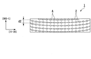
- FIG. 3 is a schematic cross-sectional view of an example of a cut surface obtained by cutting the SiC single crystal according to the present embodiment along the [1-100] direction through the center in plan view.
- FIG. 3 is a schematic cross-sectional view of an example of a cut surface obtained by cutting the SiC single crystal according to the present embodiment along the [11-20] direction through the center in plan view.
- FIG. 3 is a diagram schematically illustrating an example of an atomic arrangement plane of a SiC single crystal according to the present embodiment. It is the figure which showed typically an example of the atomic arrangement surface of the SiC single crystal in which the direction of curvature of an atomic arrangement surface changes with directions.
- FIG. 3 is a schematic cross-sectional view of an example of a cut surface obtained by cutting the SiC single crystal according to the present embodiment along the [1-100] direction through the center in plan view.
- FIG. 3 is a schematic cross-sectional view of an example of a cut surface obtained by cutting the SiC single crystal according to the present
- FIG. 3 is a diagram for specifically explaining an example of a method of measuring the amount of curvature of an atomic arrangement surface.
- FIG. 3 is a diagram for specifically explaining an example of a method of measuring the amount of curvature of an atomic arrangement surface.
- FIG. 3 is a diagram for specifically explaining an example of a method of measuring the amount of curvature of an atomic arrangement surface.
- FIG. 3 is a diagram for specifically explaining an example of a method of measuring the amount of curvature of an atomic arrangement surface.
- An example in which a radius of curvature of an atomic arrangement surface is obtained from a plurality of XRD measurement points will be described.
- FIG. 9 is a diagram for specifically explaining another example of a method for measuring the amount of curvature of an atomic arrangement surface.
- FIG. 9 is a diagram for specifically explaining another example of a method for measuring the amount of curvature of an atomic arrangement surface.
- FIG. 12B is a supplementary diagram for deriving ⁇ / 2 in FIG. 12A. It is a figure for supplementing FIG. 12A. It is a schematic diagram of an example of the manufacturing apparatus used for the sublimation method.
- FIG. 6 is a diagram for obtaining a radius of curvature of an atomic arrangement surface from a plurality of XRD measurement points in the SiC seed crystal according to the first embodiment.
- FIG. 4 is a diagram for obtaining a radius of curvature of an atomic arrangement surface from a plurality of XRD measurement points in a grown SiC single crystal according to Example 1.
- FIG. 9 is a diagram for obtaining a radius of curvature of an atomic arrangement surface from a plurality of XRD measurement points in a SiC seed crystal according to Comparative Example 1.
- FIG. 9 is a diagram for obtaining a radius of curvature of an atomic arrangement surface from a plurality of XRD measurement points in a grown SiC single crystal according to Comparative Example 1.
- FIG. 4 is a view showing measured values obtained by measuring relative positions of lattice planes of a SiC seed crystal according to Example 1.
- FIG. 4 is a view showing measured values obtained by measuring relative positions of lattice planes of a grown SiC single crystal according to Example 1.
- FIG. 9 is a view showing measured values obtained by measuring relative positions of lattice planes of a SiC seed crystal according to Comparative Example 1.
- FIG. 9 is a view showing measured values obtained by measuring relative positions of lattice planes of a grown SiC single crystal according to Comparative Example 1.
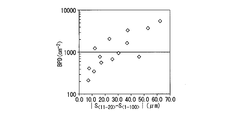
- FIG. 6 is a diagram showing relative values of the amount of curvature d1 in the [1-100] direction and the amount of curvature d2 in the [11-20] direction of a single crystal, and the density of BPD contained in the crystal growth portion.
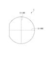
- FIG. 1 is a plan view of an example of the SiC single crystal according to the present embodiment.
- FIG. 2 is a schematic cross-sectional view of a cross section of the SiC single crystal according to the present embodiment cut along the [1-100] direction passing through the center in plan view.
- the upper side is the direction in which the carbon plane (C plane, (000-1) plane) appears when cut perpendicular to the [000-1] direction, that is, the ⁇ 0001> direction.
- FIG. 3 is a schematic cross-sectional view of the SiC single crystal according to the present embodiment taken along a [11-20] direction passing through the center in plan view and orthogonal to [1-100] shown in FIG. It is. Also in FIG.
- the upper side is the direction in which the carbon plane (C plane, (000-1) plane) appears when cut perpendicular to the [000-1] direction, that is, the ⁇ 0001> direction.
- the [1-100] direction and the [11-20] direction are representative of the ⁇ 1-100> direction and the ⁇ 11-20> direction orthogonal to the ⁇ 1-100> direction. The direction and direction were selected and illustrated. Also in the following description, description will be made using the [1-100] direction and the [11-20] direction. 2 and 3 each show a part of the SiC single crystal.
- the “center in plan view” means that the SiC single crystal to be evaluated has a circular shape in plan view, and a part thereof is missing.
- such a material for example, a SiC wafer having an orientation flat
- it means the center of the circle.
- a known method for example, a sublimation method
- a wafer or a cut body obtained by cutting a SiC single crystal ingot in a direction (excluding the vertical direction) intersecting the crystal growth direction has an elliptical shape in plan view. It means the intersection of the major axis and the minor axis of the ellipse.
- the crystal orientation and the atomic arrangement plane are represented by the following brackets as Miller indices.
- ⁇ are used to represent a surface (especially also referred to as a surface index).
- Is used to represent a specific plane and ⁇ is used to represent a generic term (collective plane) of equivalent planes due to crystal symmetry.
- ⁇ > and [] are used when indicating a direction (especially also referred to as a direction index).
- [] Is used to represent a specific direction and ⁇ > is used to represent an equivalent direction due to crystal symmetry.
- the direction index indicated by the same index as the surface index indicates the direction of the normal line of the surface.
- SiC single crystal 1 is a single crystal in which a plurality of atoms A are aligned. Therefore, as shown in FIGS. 2 and 3, when the cut surface of the SiC single crystal is viewed microscopically, an atomic arrangement surface 2 in which a plurality of atoms A are arranged is formed.
- the atom arrangement plane 2 in the cutting plane can be drawn as a line extending in a direction substantially parallel to the cutting direction obtained by connecting the atoms A arranged along the cutting plane.
- the shape of the atomic arrangement plane 2 in the cut plane may be a convex shape or a concave shape regardless of the shape of the outermost surface of the SiC single crystal 1.
- the shape of the atomic arrangement plane 2 may be different depending on the cutting direction.
- Examples of the shape of the atom arrangement surface 2 include a shape as shown in FIG. 4 and a shape as shown in FIG.
- the shape as shown in FIG. 4 is a concave shape depressed toward the center.
- the shape as shown in FIG. 5 is a potato chip type (saddle type) shape having a concave shape on a predetermined cut surface and a convex shape on a different cut surface. That is, the shape of the atom arrangement surface 2 includes a shape having the same shape in an arbitrary cutting direction and a shape having a different shape depending on the cutting direction.
- the shape of the atomic arrangement plane 2 is measured by X-ray diffraction (XRD).
- XRD X-ray diffraction
- the surface to be measured is determined according to the measurement direction. Assuming that the measurement direction is [hkill], the measurement surface needs to satisfy the relationship of (mh mk (mi n).
- m is an integer of 0 or more, and n is a natural number.
- the C plane or the Si plane may be selected, but the measurement direction is not changed in one sample.
- the X-ray diffraction data is acquired at a total of five points, for example, a center and two ends along a predetermined direction, and two midpoints between the center and the ends.
- the diffraction direction of the X-ray changes, so that the position of the ⁇ angle of the peak of the X-ray diffraction image output at the center and other portions changes.
- the bending direction of the atomic arrangement surface 2 can be obtained from the position fluctuation of the diffraction peak.
- the radius of curvature of the atomic arrangement surface 2 can be obtained from the position fluctuation of the diffraction peak, and the amount of curvature of the atomic arrangement surface 2 can also be obtained.
- X-ray diffraction data may be acquired at nine points on the same straight line passing through the center of the wafer W.
- the location where X-ray diffraction data is acquired can be arbitrarily selected. For example, it is preferable to acquire the X-ray diffraction data at each midpoint of “center, end, midpoint between center and end” along a predetermined direction.
- FIG. 6 is a schematic cross-sectional view of the wafer W.
- FIG. 6 schematically shows a cross section cut along the direction of measurement of the atomic arrangement plane, for example, along the [1-100] direction, passing through the center in plan view. Assuming that the radius of the wafer W is r, the horizontal length of the cross section is 2r.
- FIG. 6 also shows the shape of the atomic arrangement plane 22 on the wafer W. As shown in FIG. 6, the shape of the wafer W itself is flat, but the atomic arrangement surface 22 may be curved.
- the atom arrangement surface 22 shown in FIG. 6 is bilaterally symmetric and concavely curved.
- This symmetry is caused by the fact that the manufacturing conditions of the ingot are usually symmetric with respect to the central axis (the axis passing through the center of the circle in plan view and extending in the crystal growth direction).
- the symmetry does not need to be perfect symmetry, but means symmetry as an approximation that allows blurring caused by fluctuations in manufacturing conditions and the like.
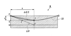
- XRD is performed on both outer peripheral edges of the wafer W, and a difference ⁇ between the measured X-ray diffraction peak angles between the two points is obtained. That is, the difference ⁇ between the X-ray diffraction peak angles at both outer peripheral ends of the wafer W is obtained. As shown in FIG. 7, this ⁇ is the difference between the measured inclinations of the atomic arrangement plane 22 at two points (that is, the inclinations of the tangents). As described above, an appropriate plane is selected according to the cut plane as the diffraction plane used for the X-ray diffraction measurement.
- FIG. 8 shows circles C that are in contact with two measured atomic arrangement planes, assuming that the curved surface of the atomic arrangement plane 22 of the wafer W is a part of a circle. From FIG. 8, it can be seen that geometrically, the central angle ⁇ of the sector including the arc having the contact at both ends becomes equal to the difference ⁇ between the measured X-ray diffraction peak angles.
- the radius of curvature of the atomic arrangement surface 22 corresponds to the radius R of the arc.
- the radius R of the arc is obtained by the following relational expression.
- the amount of curvature d of the atomic arrangement surface 22 is obtained from the radius R of the arc and the radius r of the wafer W.
- the amount of curvature d of the atomic arrangement surface 22 corresponds to a value obtained by subtracting the perpendicular distance from the center of the arc to the surface of the wafer W from the radius R of the arc.
- the distance of the perpendicular from the center of the arc to the surface of the wafer W is calculated from the three-square theorem, and the following equation holds.
- the curvature d when the radius of curvature is positive (concave surface) is defined as a positive value
- the curvature d when the radius of curvature is negative (convex) is defined as a negative value.
- R can be measured only from the measured values at both outer edges of the XRD wafer W.
- the X-ray diffraction peak angles are measured at a plurality of locations, and the curvature per unit length is converted from the following equation. For example, to improve the accuracy, it is preferable to measure the X-ray diffraction peak angle at five or more points including the center, the end, and the midpoint between the center and the end, and it is more preferable to perform the measurement at nine or more points.
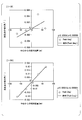
- FIG. 10 shows an example in which the radius of curvature of the atomic arrangement surface is determined from a plurality of XRD measurement points.
- the horizontal axis in FIG. 10 is the relative position from the wafer center, and the vertical axis shows the relative diffraction peak angle of each measurement point with respect to the wafer center diffraction peak angle.
- FIG. 11 schematically shows a cut surface of the wafer W cut along a measurement direction of the atomic arrangement plane, for example, along the [1-100] direction, passing through the center in plan view.
- FIG. 11 illustrates an example in which the shape of the atomic arrangement surface 22 is concavely curved.
- the diffraction peaks of the X-ray diffraction are measured at two points (two points indicated by a circle in FIG. 11) at the center of the wafer W and at a distance x from the center of the wafer W. .
- the shape of the wafer W can be made approximately symmetrical as an approximation, and it can be estimated that the atomic arrangement plane 22 becomes flat at the center of the wafer W in plan view. Therefore, as specifically shown in FIG.
- FIG. 12A shows a supplementary diagram for deriving ⁇ / 2 in FIG. 12A.
- Points P, Q, S, T, U, V, and V in FIGS. 12A and 12B indicate the same position.
- a circle C is a circle that is in contact with the atomic arrangement surface on the assumption that the curved surface of the atomic arrangement surface 22 is a part of the circle, as in FIG.
- R be the radius of the circle C.
- Point O indicates the center of circle C.
- Tangent of the straight line L P is the point P
- the tangent of the straight line L T is the point T
- linear L T ' is the point V, which is a straight line parallel to the straight line L T.
- Point H indicates the midpoint of line segment PT. The intersection of the straight line and the tangent line L T passing through the point O and the point H and Z.
- the atomic arrangement plane at the wafer center and the measurement point at each point 22 relative atomic positions can be determined.
- the relative positions of the atoms on the atomic arrangement plane are obtained at each measurement point. Therefore, the amount of curvature (y 0 , y 1 , y 2 ) of the local atomic arrangement plane can be obtained.
- the relative atomic positions of the atomic arrangement surface 22 in the entire wafer W can be shown as a graph, which is useful for intuitively grasping the arrangement of the atomic arrangement surfaces 22, 22a, and 22b.
- the SiC single crystal 1 according to the present embodiment has an atomic arrangement plane 2 (hereinafter, referred to as an atomic arrangement plane in the [1-100] direction) in a section taken along the [1-100] direction passing through the center in plan view.
- An atomic arrangement surface 2 (hereinafter, referred to as an [11-20] direction atomic arrangement surface) in a section taken along the [11-20] direction passing through the center in plan view is curved in the same direction. That is, both the [1-100] direction atomic arrangement plane and the [11-20] direction atomic arrangement plane are convex or concave. That is, the mode shown in FIG. 4 satisfies the condition of the SiC single crystal according to the present embodiment. On the other hand, the mode shown in FIG.
- the relationship of the curvature need not always be established between the [1-100] direction and the [11-20] direction, and at least one set of the ⁇ 1-100> direction and the ⁇ 1-100> direction. The relationship may be satisfied between the ⁇ 11-20> direction and the ⁇ 11-20> direction perpendicular to.
- Both the [1-100] direction atomic arrangement plane and the [11-20] direction atomic arrangement plane preferably have a concave shape with respect to the lamination plane on which the SiC single crystal is grown.
- the layer plane is the plane of the SiC single crystal in the crystal growth direction of the SiC single crystal, and corresponds to the carbon plane.
- the amount of curvature of the atomic arrangement plane 2 means the difference between the atomic position at the center of the SiC single crystal 1 in plan view and the atomic position in the [000-1] direction at the end of the SiC single crystal 1.
- the amount of curvature when the atomic arrangement surface 2 is concave toward the center in plan view is positive, and the amount of curvature when the atomic array surface 2 is convex toward the center in plan view is negative.
- a small difference between the amount of curvature d1 and the amount of curvature d2 means that the shape of the atomic arrangement surface 2 does not have anisotropy in a predetermined direction.
- the difference between the amount of curvature d1 of the atomic arrangement surface in the [1-100] direction and the amount of curvature d2 of the atomic arrangement surface in the [11-20] direction is large, the atomic arrangement surface 2 becomes large in a predetermined direction. It has a bent shape. If the shape of the atomic arrangement surface 2 has a large anisotropy in a predetermined direction, when a temperature change occurs, stress concentration tends to occur in that direction. The stress concentration induces the slip of the crystal plane, and may cause BPD.
- the bending amount d1 shows a negative value and the bending amount d2 shows a positive value.
- the bending amount d1 is ⁇
- the bending amount d2 is ⁇ .
- the absolute value of the difference between the amount of bending d1 and the amount of bending d2 is ⁇ + ⁇ . That is, the magnitude of the difference between the curving amount d1 and the curving amount d2 is necessarily larger than the curving amount d1 and the curving amount d2.
- the curving directions of the atomic arrangement plane 2 in the cutting planes in two directions are the same.
- the bending directions of the atomic arrangement planes 2 in the cutting planes in more directions are the same.
- the [1-100] direction and the [11-20] direction have been described above as examples.
- the ⁇ 1-100> direction and the ⁇ 11-20> direction orthogonal thereto are orthogonal to each other. The same can be said for a combination of the two directions.
- the crystal structure of the SiC single crystal 1 is hexagonal. Therefore, it is preferable that the bending directions in the cut surfaces cut along the six directions symmetric with respect to the center are the same. More specifically, the curved directions of the atomic arrangement planes 2 at the respective cut planes cut along six directions that are rotated by 30 ° with respect to the [1-100] direction passing through the center in a plan view may be the same. preferable.
- the atom arrangement surface 2 in an arbitrary cut surface is curved in the same direction.
- the embodiment shown in FIG. 4 corresponds to a case where the atom arrangement plane 2 in an arbitrary cut plane is curved in the same direction.
- the amount of curvature of the atomic arrangement surface 2 in each of the cut planes cut along six directions, each of which passes through the center in a plan view and is rotated by 30 ° with respect to the [1-100] direction by 30 ° is used.
- the difference between the maximum value and the minimum value is preferably 60 ⁇ m or less, more preferably 40 ⁇ m or less, and even more preferably 20 ⁇ m or less.
- the difference between the maximum value and the minimum value of the amount of curvature of the atomic arrangement plane 2 in each of the cut planes cut along nine directions rotated by 20 ° with respect to the [1-100] direction through the center in plan view is described above. It is more preferable that it is within the range.
- the difference between the maximum value and the minimum value of the amount of curvature of the atomic arrangement surface 2 in an arbitrary cut plane is preferably 60 ⁇ m or less, more preferably 40 ⁇ m or less, and further preferably 20 ⁇ m or less.
- the absolute value of the amount of curvature of the atomic arrangement surface 2 is also small.
- the difference between the maximum value and the minimum value of the amount of curvature per unit length in the outer circumferential direction of the atomic arrangement surface 2 is preferably 4 ⁇ m / cm or less, more preferably 3 ⁇ m / cm or less, More preferably, it is 2 ⁇ m / cm or less.
- the “bending amount per unit length” means a value obtained by dividing the bending amount by the diameter of the SiC single crystal.
- the SiC single crystal 1 preferably has a diameter in plan view of 140 mm or more, and more preferably 150 mm or more.
- the crystal growth conditions differ between the center and the end in plan view, and the difficulty of growing a high-quality crystal increases.
- a 6-inch SiC single crystal not only has a similar shape but a larger shape, but also has a much higher difficulty in crystal growth.
- the size of the SiC single crystal 1 in plan view increases, it is required to start crystal growth from a state in which BPD does not easily occur. That is, the value of suppressing the BPD increases as the SiC single crystal 1 having a larger diameter in plan view satisfies the predetermined condition.
- the thickness of the SiC single crystal 1 is preferably at least 500 ⁇ m, more preferably at least 750 ⁇ m, even more preferably at least 1 mm. If the thickness of SiC single crystal 1 is 500 ⁇ m or more, warpage of SiC single crystal 1 itself can be suppressed.
- the “warpage” here means the degree of deformation of the wafer. The flatter the wafer, the smaller the warpage, and the greater the curvature of the wafer, for example, in the crystal growth direction, the greater the warpage. If the SiC single crystal 1 warps itself, it becomes difficult to accurately estimate the amount of curvature of the atomic arrangement plane 2.
- the amount of warpage of the SiC single crystal 1 is preferably 5 ⁇ m or less in an arbitrary direction, and more preferably 3 ⁇ m or less.
- the amount of warpage of the SiC single crystal 1 means that when the SiC single crystal 1 is mounted on an external flat surface, the flat surface side of the surface of the SiC single crystal 1 is shifted from the mounting surface to the flat surface. It indicates the maximum value of the distance of the perpendicular line that is turned down. That is, a predetermined surface of the SiC single crystal 1 is set as a mounting surface, and an external flat surface is set as a flat surface. When the SiC single crystal 1 is mounted such that the mounting surface is in contact with the flat surface, the maximum value of the distance between the mounting surface and the flat surface is referred to as the amount of warpage.
- the generation of basal plane dislocation (BPD) in the crystal growth portion can be suppressed.
- a sublimation method is known as one of the methods for producing a SiC single crystal.
- the sublimation method is a method in which a raw material gas generated by heating a raw material is recrystallized on a single crystal (seed crystal) to obtain a large single crystal (ingot).
- seed crystal single crystal
- ingot large single crystal
- a recrystallized SiC single crystal may be referred to as a SiC ingot.
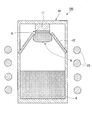
- FIG. 13 is a schematic cross-sectional view schematically showing a cross section of an example of a manufacturing apparatus used for the sublimation method.
- the manufacturing apparatus 100 has a crucible 10 and a coil 20. Between the crucible 10 and the coil 20, a heating element (not shown) that generates heat by induction heating of the coil 20 may be provided.
- the method for manufacturing the SiC single crystal, the SiC ingot, and the SiC wafer according to the present embodiment is not limited to the manufacturing apparatus shown in FIG. 13, and any manufacturing apparatus can be used.
- the crucible 10 has a crystal setting part 11 provided at a position facing the raw material G.
- the crucible 10 may have a taper guide 12 that expands in diameter from the crystal setting part 11 toward the raw material G inside.
- the raw material G, the seed crystal 5, and the SiC ingot 6 grown from the seed crystal 5 are also shown for easy understanding.
- the crystal growth plane of seed crystal 5 is a carbon plane (C plane) or a plane provided with an off angle of 0 to 10 ° from the carbon plane.
- the crystal growth surface of the seed crystal 5 is more preferably a carbon surface or a surface having an off angle of 0 to 5 ° from the carbon surface.
- the seed crystal 5 corresponds to the SiC single crystal 1 according to the present embodiment.
- the seed crystal 5 is used by cutting out a part of an already produced SiC ingot. For this reason, the seed crystal 5 can be selected from the SiC ingots already manufactured that meet predetermined conditions.
- a seed crystal 5 cut out from an SiC ingot in which the [1-100] direction atomic arrangement plane and the [11-20] direction atomic arrangement plane passing through the center in plan view and curved in the same direction is used.
- SiSiC ingot 6 growing from seed crystal 5 inherits much of the crystal information of seed crystal 5. Therefore, by setting the bending direction of the atomic arrangement surface of the seed crystal 5, the bending direction of the atomic arrangement surface of the SiC ingot 6 can also be within a predetermined range.
- ⁇ Also as the seed crystal 5, it is preferable to use a seed produced by a RAF method (repeated-a-face method).
- the RAF method is a method of performing c-plane growth after performing a-plane growth at least once or more.
- an SiC single crystal with few screw dislocations, stacking faults, and BPD can be manufactured. This is because screw dislocations, stacking faults, and BPDs of the SiC single crystal after the a-plane growth are not carried over to the SiC single crystal after the c-plane growth.
- the thickness of the seed crystal 5 is preferably 1 mm or more, more preferably 2 mm or more, even more preferably 3 mm or more. If the thickness of the seed crystal 5 is large, the seed crystal 5 itself can be prevented from being curved. When the seed crystal 5 is curved, the SiC ingot 6 growing on the seed crystal 5 is affected by the curvature of the seed crystal 5 itself and the curvature of the atomic arrangement surface 2 in the seed crystal 5. That is, even if the atom arrangement surface 2 of the seed crystal 5 has a predetermined curved surface, the curved surface may not be carried over to the SiC ingot 6 in some cases.
- the prepared seed crystal 5 is fixed to the crystal setting part 11 using an adhesive or the like. It is preferable to use an adhesive having a small anisotropy in the surface shape of the adhesive, and it is preferable that the adhesive does not deform the seed crystal 5 in a specific direction before and after the application. When the adhesive has anisotropy, stress is applied to the grown SiC ingot 6 due to the anisotropy of the adhesive during crystal growth, and the atom arrangement surface may be deformed.
- the crucible 10 is heated to sublimate the raw material G.
- the rotation speed is preferably at least 0.1 rpm, more preferably at least 0.3 rpm, and even more preferably at least 0.5 rpm.
- the cutting direction is perpendicular to ⁇ 0001> or cut in the direction with an off angle of 0 to 10 ° to produce a wafer that is parallel to the C plane or has a surface with an off angle of 0 to 10 ° from the C plane. I do.
- the wafer may be mirror-finished on the (0001) surface side, that is, on the Si surface side.
- the Si surface is a surface on which epitaxial growth is usually performed. Since the SiC ingot 6 has a small BPD, an SiC wafer having a small BPD can be obtained. By using an SiC wafer with a small number of BPDs as killer defects, a high-quality SiC epitaxial wafer can be obtained, and the yield of SiC devices can be increased.
- Example 1 a seed crystal composed of a 4H—SiC single crystal in which both the ⁇ 1-100> atomic arrangement plane and the ⁇ 11-20> atomic arrangement plane orthogonal to the ⁇ 1-100> are curved in the same direction is used. Got ready. The diameter of the seed crystal was 16 cm. As the seed crystal, a SiC single crystal having a concave shape in the [1-100] direction and the [11-20] direction with respect to the carbon surface was used.
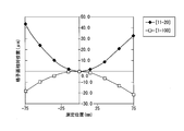
- FIG. 14 shows the results of the X-ray diffraction measurement in the [1-100] and [11-20] directions. In the figure, the measurement results at the XRD measurement points are plotted.
- the horizontal axis of FIG. 14 is the relative position of the seed crystal from the center in plan view, and the vertical axis is the relative diffraction peak angle of each measurement point with respect to the central diffraction peak angle of the seed crystal.
- the atomic arrangement plane was measured by the method described in the above (specific description of the method for measuring the amount of curvature of the atomic arrangement plane).
- This seed crystal was placed at a position facing the raw material such that the atomic arrangement plane was concave with respect to the stacking plane. Then, the crucible was heated to sublimate the raw material, and a SiC single crystal was grown to a thickness of about 20 mm on the layered surface of the seed crystal to obtain a SiC ingot.
- the BPD density was 350 / cm ⁇ 2 . Further, the wafers manufactured from the obtained SiC ingots were confirmed by X-ray diffraction (XRD) by using the same method as the SiC seed crystal for the shape of the [1-100] direction atomic arrangement plane and the [11-20] direction atomic arrangement plane. .
- XRD X-ray diffraction
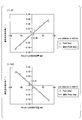
- FIG. 15 shows the measurement results in the [1-100] and [11-20] directions of the X-ray diffraction measurement.
- the horizontal axis of FIG. 15 is the relative position from the center of the wafer in plan view, and the vertical axis is the relative diffraction peak angle of each measurement point with respect to the central diffraction peak angle of the wafer.
- all of the obtained wafers SiC ingots were curved in the same direction as the seed crystal.
- the atomic plane arrangement of the crystal of Example 1 was measured using another measuring method.
- This other method is the method described in the above (the description of another method for measuring the amount of curvature of the atomic arrangement surface).
- the shape of the [1-100] direction atomic arrangement plane and the [11-20] direction atomic arrangement plane of the same seed crystal as in Example 1 and a wafer (SiC ingot) obtained from the seed crystal were measured. did.
- the results are shown in FIGS. 18 and 19, respectively. In the figure, the relative positions of the lattice planes at the measurement positions are plotted. It was confirmed that the obtained SiC ingots were all curved in the same direction as the seed crystal.
- Comparative Example 1 a seed crystal in which the ⁇ 1-100> atomic arrangement plane and the ⁇ 11-20> atomic arrangement plane were curved in different directions was prepared.
- the diameter of the seed crystal was 16 cm.
- As the seed crystal an SiC single crystal having a different curvature direction with respect to the carbon surface between the [1-100] direction and the [11-20] direction was used.
- FIG. 16 shows the results of the X-ray diffraction measurement in the [1-100] and [11-20] directions. In the figure, the measurement results at the XRD measurement points are plotted. From the results of the X-ray diffraction measurement, a convex surface having a radius of curvature of ⁇ 764 m and a curvature of ⁇ 3.7 ⁇ m in the [1-100] direction, a concave surface having a radius of curvature of 93 m and a curvature of 30.2 ⁇ m in the [11-20] direction were obtained. calculated.
- the amount of curvature is different in the negative direction in the [1-100] direction and different in the positive direction in the [11-20] direction, and the atom arrangement surface 2 has a convex shape on one cut surface and a concave shape on a different cut surface. It had a mold (saddle) shape.
- Example 2 ⁇ Circle around (2) ⁇ As in Example 1, a SiC single crystal was grown on the seed crystal stacking surface of Comparative Example 1 by about 20 mm to obtain a SiC ingot.
- the BPD density in the obtained SiC ingot was as high as 3360 / cm ⁇ 2 .
- the wafers fabricated from the obtained SiC ingots were confirmed by X-ray diffraction (XRD) by using the same method as that for the seed crystal in terms of the [1-100] direction atomic arrangement plane and the [11-20] direction atomic arrangement plane.
- XRD X-ray diffraction
- the radius of curvature of the atomic arrangement surface was determined from a plurality of XRD measurement points.
- FIG. 17 shows the results of the X-ray diffraction measurement in the [1-100] and [11-20] directions. In the figure, the measurement results at the XRD measurement points are plotted.
- the radius of curvature was -138 m in the [1-100] direction and a convex surface with a curvature of -20.4 ⁇ m, and in the [11-20] direction, a concave surface with a radius of curvature of 71 m and a curvature of 39.6 ⁇ m.
- the amount of curvature is different in the negative direction in the [1-100] direction and different in the positive direction in the [11-20] direction, and the atom arrangement surface 2 has a convex shape on one cut surface and a concave shape on a different cut surface. It had a mold (saddle) shape.
- a potato chip type (saddle type) seed crystal was used in which the atom arrangement surface was convex on one cut surface and concave on a different cut surface. SiC ingots and wafers were made.
- the crystal of Comparative Example 1 was obtained from the same seed crystal and the seed crystal thereof as in Comparative Example 1 by the method described in (Description of Another Measurement Method of Curvature of Atomic Array Surface).
- the shapes of the [1-100] direction atomic arrangement plane and the [11-20] direction atomic arrangement plane were measured. The results are shown in FIGS. 20 and 21, respectively. It was confirmed that the obtained wafer and SiC ingot were curved in different directions in the [1-100] atomic arrangement plane and the [11-20] atomic arrangement plane, similarly to the seed crystal.
- the measurement results of the relative positions of the atoms on the atomic arrangement plane shown in FIGS. 18 to 21 are reference data for intuitively grasping the arrangement of the atomic arrangement plane.
- a plurality of seed crystals having different amounts of curvature in the [1-100] direction atomic arrangement plane and in the [11-20] direction atomic arrangement plane were prepared, and a SiC single crystal was grown on the seed crystal. Then, the BPD density contained in the crystal growth portion grown from the seed crystal was determined.
- a SiC single crystal having a diameter of 16 cm was used as a seed crystal.
- a SiC single crystal was grown by about 20 mm.
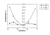
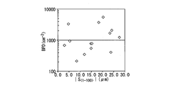
- FIGS. 22A and 22B are diagrams showing the relationship between BPD densities contained in a crystal growth portion when a single crystal is grown on a predetermined SiC single crystal.
- FIG. 22A shows the relationship between the absolute value of the amount of curvature d1 of the atomic arrangement surface 2 in the section taken along the [1-100] direction passing through the center in plan view and the BPD density included in the crystal growth portion.
- FIG. The horizontal axis indicates the absolute value of the amount of curvature d1 of the atomic arrangement plane 2 in the cut plane cut along the [1-100] direction, and the vertical axis indicates the BPD density included in the crystal growth portion.
- FIG. 22A shows the relationship between the absolute value of the amount of curvature d1 of the atomic arrangement surface 2 in the section taken along the [1-100] direction passing through the center in plan view and the BPD density included in the crystal growth portion.
- FIG. The horizontal axis indicates the absolute value of the amount of curvature d1 of the
- FIG. 22B is a graph showing the relationship between the absolute value of the amount of curvature d2 of the atomic arrangement surface 2 in the cut plane cut along the [11-20] direction passing through the center in plan view and the density of the BPD included in the crystal growth portion.
- FIG. The horizontal axis is the absolute value of the amount of curvature d2 of the atomic arrangement surface 2 in the cut plane cut along the [11-20] direction.
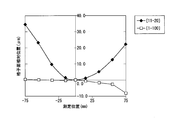
- FIG. 22C is a diagram showing the relative values of the amount of curvature d1 and the amount of curvature d2 and the density of the BPD contained in the crystal growth portion.
- the horizontal axis is a relative value between the bending amount d1 and the bending amount d2.
Landscapes
- Chemical & Material Sciences (AREA)
- Engineering & Computer Science (AREA)
- Materials Engineering (AREA)
- Metallurgy (AREA)
- Organic Chemistry (AREA)
- Crystallography & Structural Chemistry (AREA)
- Inorganic Chemistry (AREA)
- Chemical Kinetics & Catalysis (AREA)
- General Chemical & Material Sciences (AREA)
- Mechanical Engineering (AREA)
- Crystals, And After-Treatments Of Crystals (AREA)
Priority Applications (2)
| Application Number | Priority Date | Filing Date | Title |
|---|---|---|---|
| US17/267,691 US20210189596A1 (en) | 2018-08-13 | 2019-08-13 | SiC SINGLE CRYSTAL, METHOD OF MANUFACTURING SiC INGOT, AND METHOD OF MANUFACTURING SiC WAFER |
| CN201980053250.2A CN112639177A (zh) | 2018-08-13 | 2019-08-13 | SiC单晶、SiC晶锭的制造方法和SiC晶片的制造方法 |
Applications Claiming Priority (2)
| Application Number | Priority Date | Filing Date | Title |
|---|---|---|---|
| JP2018-152391 | 2018-08-13 | ||
| JP2018152391A JP2020026376A (ja) | 2018-08-13 | 2018-08-13 | SiC単結晶、SiCインゴットの製造方法及びSiCウェハの製造方法 |
Publications (1)
| Publication Number | Publication Date |
|---|---|
| WO2020036170A1 true WO2020036170A1 (ja) | 2020-02-20 |
Family
ID=69525367
Family Applications (1)
| Application Number | Title | Priority Date | Filing Date |
|---|---|---|---|
| PCT/JP2019/031814 Ceased WO2020036170A1 (ja) | 2018-08-13 | 2019-08-13 | SiC単結晶、SiCインゴットの製造方法及びSiCウェハの製造方法 |
Country Status (4)
| Country | Link |
|---|---|
| US (1) | US20210189596A1 (https=) |
| JP (1) | JP2020026376A (https=) |
| CN (1) | CN112639177A (https=) |
| WO (1) | WO2020036170A1 (https=) |
Families Citing this family (1)
| Publication number | Priority date | Publication date | Assignee | Title |
|---|---|---|---|---|
| JP7190841B2 (ja) | 2018-08-13 | 2022-12-16 | 昭和電工株式会社 | SiCインゴットの製造方法及びSiCウェハの製造方法 |
Citations (3)
| Publication number | Priority date | Publication date | Assignee | Title |
|---|---|---|---|---|
| WO2009035095A1 (ja) * | 2007-09-12 | 2009-03-19 | Showa Denko K.K. | エピタキシャルSiC単結晶基板及びエピタキシャルSiC単結晶基板の製造方法 |
| JP2011111372A (ja) * | 2009-11-27 | 2011-06-09 | Showa Denko Kk | 炭化珪素単結晶及びその製造方法、並びに炭化珪素単結晶ウェーハ及び炭化珪素単結晶インゴット |
| JP2013136494A (ja) * | 2011-12-28 | 2013-07-11 | Toyota Central R&D Labs Inc | 単結晶製造装置、SiC単結晶、ウェハ、及び、半導体デバイス |
Family Cites Families (3)
| Publication number | Priority date | Publication date | Assignee | Title |
|---|---|---|---|---|
| DE19823962A1 (de) * | 1998-05-28 | 1999-12-02 | Wacker Siltronic Halbleitermat | Verfahren zur Herstellung eines Einkristalls |
| JP4470690B2 (ja) * | 2004-10-29 | 2010-06-02 | 住友電気工業株式会社 | 炭化珪素単結晶、炭化珪素基板および炭化珪素単結晶の製造方法 |
| JP7190841B2 (ja) * | 2018-08-13 | 2022-12-16 | 昭和電工株式会社 | SiCインゴットの製造方法及びSiCウェハの製造方法 |
-
2018
- 2018-08-13 JP JP2018152391A patent/JP2020026376A/ja active Pending
-
2019
- 2019-08-13 US US17/267,691 patent/US20210189596A1/en not_active Abandoned
- 2019-08-13 WO PCT/JP2019/031814 patent/WO2020036170A1/ja not_active Ceased
- 2019-08-13 CN CN201980053250.2A patent/CN112639177A/zh not_active Withdrawn
Patent Citations (3)
| Publication number | Priority date | Publication date | Assignee | Title |
|---|---|---|---|---|
| WO2009035095A1 (ja) * | 2007-09-12 | 2009-03-19 | Showa Denko K.K. | エピタキシャルSiC単結晶基板及びエピタキシャルSiC単結晶基板の製造方法 |
| JP2011111372A (ja) * | 2009-11-27 | 2011-06-09 | Showa Denko Kk | 炭化珪素単結晶及びその製造方法、並びに炭化珪素単結晶ウェーハ及び炭化珪素単結晶インゴット |
| JP2013136494A (ja) * | 2011-12-28 | 2013-07-11 | Toyota Central R&D Labs Inc | 単結晶製造装置、SiC単結晶、ウェハ、及び、半導体デバイス |
Also Published As
| Publication number | Publication date |
|---|---|
| CN112639177A (zh) | 2021-04-09 |
| JP2020026376A (ja) | 2020-02-20 |
| US20210189596A1 (en) | 2021-06-24 |
Similar Documents
| Publication | Publication Date | Title |
|---|---|---|
| US11905621B2 (en) | SiC single crystal, method of manufacturing SiC ingot, and method of manufacturing SiC wafer | |
| JP5273741B2 (ja) | エピタキシャルSiC単結晶基板及びエピタキシャルSiC単結晶基板の製造方法 | |
| US10837123B2 (en) | Method of manufacturing SiC ingot | |
| JP7571902B2 (ja) | SiC単結晶、SiC種結晶及びSiCインゴットの製造方法 | |
| JP6120742B2 (ja) | 単結晶インゴットの製造方法、単結晶基板の製造方法、および半導体装置の製造方法 | |
| JP2010076967A (ja) | 炭化ケイ素基板の製造方法および炭化ケイ素基板 | |
| CN109957839B (zh) | SiC单晶的加工方法及SiC锭的制造方法 | |
| JP6583989B2 (ja) | SiC単結晶シード、SiCインゴット、SiC単結晶シードの製造方法及びSiC単結晶インゴットの製造方法 | |
| JP6722578B2 (ja) | SiCウェハの製造方法 | |
| WO2020036170A1 (ja) | SiC単結晶、SiCインゴットの製造方法及びSiCウェハの製造方法 | |
| WO2020036167A1 (ja) | SiC単結晶の貼合方法、SiCインゴットの製造方法及びSiC単結晶成長用台座 | |
| WO2020036166A1 (ja) | SiC単結晶の評価方法及びSiCウェハの製造方法 | |
| JP6647040B2 (ja) | 種結晶、種結晶の製造方法、SiCインゴットの製造方法及びSiCウェハの製造方法 | |
| US20190360118A1 (en) | SiC SINGLE CRYSTAL COMPOSITE AND SiC INGOT | |
| JP6971144B2 (ja) | 台座、SiC単結晶の製造装置および製造方法 | |
| US20260022493A1 (en) | Sic single crystal, sic substrate and sic epitaxial wafer | |
| JP2024088302A (ja) | SiC基板及びSiCエピタキシャルウェハ |
Legal Events
| Date | Code | Title | Description |
|---|---|---|---|
| 121 | Ep: the epo has been informed by wipo that ep was designated in this application |
Ref document number: 19849805 Country of ref document: EP Kind code of ref document: A1 |
|
| NENP | Non-entry into the national phase |
Ref country code: DE |
|
| 122 | Ep: pct application non-entry in european phase |
Ref document number: 19849805 Country of ref document: EP Kind code of ref document: A1 |