WO2020031578A1 - 光学ユニット - Google Patents
光学ユニット Download PDFInfo
- Publication number
- WO2020031578A1 WO2020031578A1 PCT/JP2019/026757 JP2019026757W WO2020031578A1 WO 2020031578 A1 WO2020031578 A1 WO 2020031578A1 JP 2019026757 W JP2019026757 W JP 2019026757W WO 2020031578 A1 WO2020031578 A1 WO 2020031578A1
- Authority
- WO
- WIPO (PCT)
- Prior art keywords
- optical
- optical module
- optical unit
- circuit board
- heat
- Prior art date
- Legal status (The legal status is an assumption and is not a legal conclusion. Google has not performed a legal analysis and makes no representation as to the accuracy of the status listed.)
- Ceased
Links
Images






Classifications
-
- G—PHYSICS
- G02—OPTICS
- G02B—OPTICAL ELEMENTS, SYSTEMS OR APPARATUS
- G02B7/00—Mountings, adjusting means, or light-tight connections, for optical elements
- G02B7/02—Mountings, adjusting means, or light-tight connections, for optical elements for lenses
- G02B7/028—Mountings, adjusting means, or light-tight connections, for optical elements for lenses with means for compensating for changes in temperature or for controlling the temperature; thermal stabilisation
-
- G—PHYSICS
- G02—OPTICS
- G02B—OPTICAL ELEMENTS, SYSTEMS OR APPARATUS
- G02B27/00—Optical systems or apparatus not provided for by any of the groups G02B1/00 - G02B26/00, G02B30/00
- G02B27/64—Imaging systems using optical elements for stabilisation of the lateral and angular position of the image
- G02B27/646—Imaging systems using optical elements for stabilisation of the lateral and angular position of the image compensating for small deviations, e.g. due to vibration or shake
-
- G—PHYSICS
- G03—PHOTOGRAPHY; CINEMATOGRAPHY; ANALOGOUS TECHNIQUES USING WAVES OTHER THAN OPTICAL WAVES; ELECTROGRAPHY; HOLOGRAPHY
- G03B—APPARATUS OR ARRANGEMENTS FOR TAKING PHOTOGRAPHS OR FOR PROJECTING OR VIEWING THEM; APPARATUS OR ARRANGEMENTS EMPLOYING ANALOGOUS TECHNIQUES USING WAVES OTHER THAN OPTICAL WAVES; ACCESSORIES THEREFOR
- G03B17/00—Details of cameras or camera bodies; Accessories therefor
- G03B17/55—Details of cameras or camera bodies; Accessories therefor with provision for heating or cooling, e.g. in aircraft
-
- G—PHYSICS
- G03—PHOTOGRAPHY; CINEMATOGRAPHY; ANALOGOUS TECHNIQUES USING WAVES OTHER THAN OPTICAL WAVES; ELECTROGRAPHY; HOLOGRAPHY
- G03B—APPARATUS OR ARRANGEMENTS FOR TAKING PHOTOGRAPHS OR FOR PROJECTING OR VIEWING THEM; APPARATUS OR ARRANGEMENTS EMPLOYING ANALOGOUS TECHNIQUES USING WAVES OTHER THAN OPTICAL WAVES; ACCESSORIES THEREFOR
- G03B5/00—Adjustment of optical system relative to image or object surface other than for focusing
-
- G—PHYSICS
- G03—PHOTOGRAPHY; CINEMATOGRAPHY; ANALOGOUS TECHNIQUES USING WAVES OTHER THAN OPTICAL WAVES; ELECTROGRAPHY; HOLOGRAPHY
- G03B—APPARATUS OR ARRANGEMENTS FOR TAKING PHOTOGRAPHS OR FOR PROJECTING OR VIEWING THEM; APPARATUS OR ARRANGEMENTS EMPLOYING ANALOGOUS TECHNIQUES USING WAVES OTHER THAN OPTICAL WAVES; ACCESSORIES THEREFOR
- G03B5/00—Adjustment of optical system relative to image or object surface other than for focusing
- G03B5/06—Swinging lens about normal to the optical axis
-
- H—ELECTRICITY
- H04—ELECTRIC COMMUNICATION TECHNIQUE
- H04N—PICTORIAL COMMUNICATION, e.g. TELEVISION
- H04N23/00—Cameras or camera modules comprising electronic image sensors; Control thereof
- H04N23/50—Constructional details
- H04N23/52—Elements optimising image sensor operation, e.g. for electromagnetic interference [EMI] protection or temperature control by heat transfer or cooling elements
-
- G—PHYSICS
- G03—PHOTOGRAPHY; CINEMATOGRAPHY; ANALOGOUS TECHNIQUES USING WAVES OTHER THAN OPTICAL WAVES; ELECTROGRAPHY; HOLOGRAPHY
- G03B—APPARATUS OR ARRANGEMENTS FOR TAKING PHOTOGRAPHS OR FOR PROJECTING OR VIEWING THEM; APPARATUS OR ARRANGEMENTS EMPLOYING ANALOGOUS TECHNIQUES USING WAVES OTHER THAN OPTICAL WAVES; ACCESSORIES THEREFOR
- G03B2205/00—Adjustment of optical system relative to image or object surface other than for focusing
- G03B2205/0007—Movement of one or more optical elements for control of motion blur
- G03B2205/0023—Movement of one or more optical elements for control of motion blur by tilting or inclining one or more optical elements with respect to the optical axis
-
- G—PHYSICS
- G03—PHOTOGRAPHY; CINEMATOGRAPHY; ANALOGOUS TECHNIQUES USING WAVES OTHER THAN OPTICAL WAVES; ELECTROGRAPHY; HOLOGRAPHY
- G03B—APPARATUS OR ARRANGEMENTS FOR TAKING PHOTOGRAPHS OR FOR PROJECTING OR VIEWING THEM; APPARATUS OR ARRANGEMENTS EMPLOYING ANALOGOUS TECHNIQUES USING WAVES OTHER THAN OPTICAL WAVES; ACCESSORIES THEREFOR
- G03B2205/00—Adjustment of optical system relative to image or object surface other than for focusing
- G03B2205/0053—Driving means for the movement of one or more optical element
- G03B2205/0069—Driving means for the movement of one or more optical element using electromagnetic actuators, e.g. voice coils
Definitions
- the present invention relates to an optical unit in which heat dissipation of an optical module is considered.
- the optical unit 100 is provided with the gimbal mechanism 30 using the corner of the optical module 10 and the corner of the rectangular cylindrical body 210 of the fixed body 20. That is, the rectangular movable frame 32 is disposed between the rectangular second frame 42 of the optical module 10 and the rectangular frame 25 fixed to the rectangular cylindrical body 210, and the first corner 321 of the movable frame 32 and A third corner 323 opposed thereto is swingably supported by two corresponding corners of the rectangular frame 25, and a second corner 322 of the movable frame 32 and a fourth corner 324 opposed thereto are provided.
- an optical module provided in the optical unit for example, a camera module or the like also supports these high-definition images, so that the number of pixels is increased and the density of sensors is increased.
- the amount of heat generated in the camera module increases.
- the camera module for example, the substrate on which the imaging element is provided is deformed by heat generation, the focal length with the subject is shifted, and accurate imaging may not be performed.
- the present invention has been made in view of the above problems, and has as its object to provide an optical unit in which heat dissipation in an optical module is considered.
- an optical unit includes a movable body including an optical module, and a fixed body that holds the movable body in a displaceable state, wherein the movable body is provided in the optical module. It has a circuit board provided, and at least one heat dissipation member arranged around the optical module, wherein the heat dissipation member is connected to the circuit board so as to be able to conduct heat. .
- the heat radiation member is connected to the circuit board so as to conduct heat.
- the heat generated in the optical module is conducted to the heat radiating member through the circuit board.
- the heat generated in the optical module is radiated by the heat radiating member, so that the optical module can be maintained at an appropriate temperature, and the performance of the optical module can be maintained.
- the heat dissipation member is formed of a metal material, and the heat dissipation member is connected to a metal foil formed on the circuit board by soldering.
- the heat radiating member formed of the metal material is connected to the metal foil formed on the circuit board by soldering, it is possible to ensure heat conduction from the circuit board to the heat radiating member. Can be. Further, by using a metal material for the heat radiating member, the thermal conductivity can be improved, and the heat of the optical module can be efficiently radiated.
- shake correction for driving the movable body around a first axis that intersects the optical axis direction of the optical module and around a second axis that intersects the optical axis direction and the first axis.
- the shake correction drive mechanism includes a magnet provided on the movable body side, and a coil provided on the fixed body side, the heat radiation member is configured as a magnetic body, and the optical axis Wherein the heat radiating member is arranged between the optical module and the magnet in a direction intersecting with the magnet.
- some of the optical modules include a magnetic circuit for correcting pitching (vertical vibration) and yawing (lateral vibration).
- the housing of the optical module in the optical module including the magnetic circuit is made of a non-magnetic material, the magnetism of the magnetic circuit leaks out of the optical module, and the shake correction drive in the optical unit according to the present invention. May interfere with the mechanism.
- the heat dissipation member is configured as a magnetic material, and the heat dissipation member is arranged between the optical module and the magnet in a direction intersecting with the optical axis. Accordingly, when the housing of the optical module is a non-magnetic material, the heat radiating member, which is a magnetic material, functions as a back yoke, and it is possible to suppress interference between the magnetic circuit and the shake correction drive mechanism. Therefore, it is possible to suppress a malfunction or the like in the shake correction driving mechanism.
- the heat dissipation member is configured as a frame-like member surrounding the optical module around the optical axis of the optical module.
- the “frame member surrounding the optical module” in the present specification includes not only a form surrounding the optical module with a single member but also a form surrounding the optical module by connecting a plurality of heat dissipation members, and further includes an optical axis.
- the frame-shaped member has a uniform height, or includes a form having an uneven portion in at least one of an optical axis direction and a direction intersecting the optical axis as appropriate.
- the heat dissipation member is configured as a frame-like member surrounding the optical module around the optical axis of the optical module, the surface area of the heat dissipation member can be increased, and heat dissipation can be improved. it can.
- the heat radiation member is arranged around the optical axis of the optical module at an interval, and faces the magnet.
- the heat radiating member is disposed so as to face the magnet at an interval around the optical axis of the optical module, heat radiation in the optical module, the shake correcting drive mechanism, and the magnetic circuit It is possible to reduce the weight of the optical unit while simultaneously suppressing interference with the optical unit.
- the circuit board is provided on a side opposite to a subject side of the optical module, and includes a protruding portion projecting from the optical module in a direction intersecting an optical axis of the optical module, At least a part of the heat dissipating member is arranged on the protruding portion.
- the circuit is arranged in a direction intersecting the optical axis.
- the heat radiating member can be arranged in a region occupied by the substrate, and the size of the optical module in a direction intersecting with the optical axis can be reduced.
- At least a part of the heat radiating member overlaps with the optical module in an optical axis direction of the optical module.
- At least a part of the heat radiating member overlaps the optical module in the optical axis direction of the optical module, so that the size of the optical module in the optical axis direction can be reduced.
- the heat radiation member is connected to the circuit board so as to be able to conduct heat.
- the heat generated in the optical module is conducted to the heat radiating member through the circuit board.
- the heat generated in the optical module is radiated by the heat radiating member, so that the optical module can be maintained at an appropriate temperature, and the performance of the optical module can be maintained.
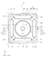
- FIG. 4 is a perspective view showing the outer casing of the optical unit according to the present invention in a see-through manner.
- FIG. 4 is a plan view showing the outer casing of the optical unit according to the present invention in a see-through manner.
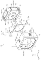
- FIG. 2 is an exploded perspective view of the optical unit according to the present invention.
- FIG. 4 is a perspective view illustrating a gimbal mechanism, an intermediate frame, a first bearing, a second bearing, and an elastic member of the optical unit.
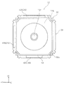
- FIG. 1 is a perspective view showing a first embodiment of an optical module and a heat dissipation member according to the present invention.
- FIG. 2 is a plan view showing a first embodiment of the optical module and the heat dissipation member according to the present invention.
- FIG. 1 is a perspective view showing a first embodiment of an optical module and a heat dissipation member according to the present invention.
- FIG. 2 is a plan view showing a first embodiment of the optical module and the heat diss
- FIG. 4 is a schematic diagram showing a connection state between a circuit board of the optical module and a heat radiating member.
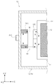
- FIG. 4 is a side sectional view showing a relationship between a heat radiating member and a shake correction drive mechanism.
- FIG. 4 is a side sectional view showing a modified form of a connection state between a circuit board of the optical module and a heat radiating member.
- FIG. 6 is a perspective view showing a second embodiment of the optical module and the heat radiation member according to the present invention.
- FIG. 6 is a plan view showing a second embodiment of the optical module and the heat dissipation member according to the present invention.
- the optical unit 10 includes a movable body 14 having an optical module 12, a fixed body 16 that holds the movable body 14 at least in a displaceable direction in a pitching (vertical vibration) direction Y and a yawing (lateral vibration) direction X, and an optical module. 12 and a first support portion 18 that supports the movable body 14 swingably about a first axis L1 intersecting with the optical axis direction Z, and a second axis that intersects with the optical axis direction Z and the first axis L1 direction.
- a gimbal mechanism 22 including a second support portion 20 that is swingably supported by a member on the fixed body 16 side around L2, and a shake correction device that drives the movable body 14 around the first axis L1 and around the second axis L2.
- a driving mechanism 24 is provided.
- the optical unit 10 is an optical unit having a function of correcting pitching (vertical vibration), yawing (lateral vibration), and rolling (vibration around the optical axis L) of the optical module 12.
- the optical module 12 is used as, for example, a thin camera mounted on a camera-equipped mobile phone, a tablet PC, or the like.
- An actuator unit that holds the optical module 12 and corrects the pitching direction Y, the yawing direction X, and the rolling direction R generated in the optical module 12 is a main configuration of the optical unit 10.
- a specific configuration of the optical unit 10 will be described in detail.
- the movable body 14 is attached to the fixed body 16 via a gimbal mechanism 22.
- the fixed body 16 includes, as an example, an outer casing 26, a coil mounting frame 28 assembled in the outer casing 26, and a second axis L 2 of the outer casing 26.
- a second bearing member 30 attached to the inner surface of the corner portion in the direction.
- the outer casing 26 has a window 26a on the front surface on the subject side + Z, and has a structure in which the rear surface on the opposite side -Z from the subject is open, and is a rectangular container-shaped member slightly larger than the optical module 12. It is configured.
- the coil mounting frame 28 has a rectangular frame-shaped flat plate portion 28 a having a central portion opened on the subject side + Z, and is provided on three sides of the flat plate portion 28 a in the optical axis direction Z. It is constituted by forming three coil mounting plates 28b that are bent 90 ° on the opposite side -Z to the subject so as to follow.
- Two sets of coils 32A and 32B (FIG. 2) for pitching correction and yaw correction and a set of coils 32C (FIGS. 2 and 3) for rolling correction are provided on the inner surface of the three coil mounting plates 28b.
- a pattern substrate (coil substrate) in which coils are taken in a substrate wiring as a pattern is adopted as the coils 32A, 32B, and 32C.
- wound coils can be used instead of such a pattern substrate.
- three magnetic sensors (Hall elements) 34A, 34B, 34C are provided.
- a thermistor 36 that detects a temperature change of the coil 32A and uses the detected temperature change to correct the detection values of the magnetic sensors 34A, 34B, 34C. Is provided.
- the second bearing member 30 is a block-shaped member having a trapezoidal cross section that is long in the optical axis direction Z, and has a concave portion 30a (FIG. 3) for receiving and engaging the second support portion 20 on the inner surface thereof.
- the gimbal mechanism 22 includes a gimbal frame portion 22a disposed on one of the object side + Z of the optical module 12 and the opposite side -Z of the object, and an optical axis direction Z from the gimbal frame portion 22a. And a second support portion extending from the gimbal frame portion 22a in the optical axis direction Z and having a second support portion 20. Setting part 22c.
- the gimbal frame section 22a is arranged at + Z on the object side of the optical module 12 as an example.
- An opening 22d is formed at the center of the gimbal frame 22a on the light incident side of the optical module 12.
- the gimbal frame portion 22a has a rectangular frame-shaped base frame 22e having a circular opening 22d formed at the center, and extends in the first axis L1 direction around the optical axis L from four corners of the base frame 22e.
- the first extending portion 22f and the second extending portion 22g extending in the direction of the second axis L2 are formed in an X-shape.
- the gimbal mechanism 22 in the present embodiment is formed by a metal plate as an example, and the first and second extending portions 22f and 22g of the X-shaped gimbal frame portion 22a are formed to be long in the extending direction. By bending these tips, a first support portion extending portion 22b and a second support portion extending portion 22c are formed.
- the first support portion 18 is provided on the inner surface of the extension portion 22b for the first support portion facing the movable body 14.
- the first support portion 18 is configured by a metal member formed on a convex curved surface.
- the first support portion 18 has a projection formed on the first support portion extending portion 22b by a press or the like. Alternatively, it is attached by welding directly to the first supporting portion extending portion 22b.
- a second support portion 20 is provided on an outer surface of the second support portion extending portion 22c facing the fixed body 16.
- the second support portion 20 is configured by a metal member formed on a convex curved surface.
- the second support portion 20 has a protruding portion formed by pressing or the like on the second support portion extending portion 22c. Alternatively, it is attached by welding directly to the second support portion extending portion 22c.
- the movable body 14 includes the optical module 12, a holder frame 38, and an intermediate frame 40.
- the optical module 12 includes a lens 12a on the subject side + Z, and includes an optical device and the like for capturing an image inside a housing 12b having a rectangular housing shape.
- the holder frame 38 is configured as a rectangular frame-shaped member (FIG. 6) provided so as to surround the remaining four surfaces excluding the front surface on which the lens 12a of the optical module 12 is provided and the rear surface on the opposite side.
- Two sets of magnets 42A and 42B for detecting and correcting pitching and yawing and a set of magnets 42C for detecting and correcting rolling are mounted on the outer surfaces of the holder frame 38 by using three surfaces thereof. .
- the pair of the coil 32A and the magnet 42A and the pair of the coil 32B and the magnet 42B constitute a shake correction drive mechanism 24 for correcting the attitude of the movable body 14.
- the pitching and yawing of the movable body 14 are corrected by the shake correction drive mechanism 24.
- the pair of the coil 32C and the magnet 42C forms a rolling drive mechanism 46.
- the rolling of the movable body 14 is corrected by the rolling drive mechanism 46.
- the intermediate frame body 40 is configured as a member formed by bending a metal flat plate provided so as to wrap the holder frame 38 from the subject side + Z (FIG. 3).
- the intermediate frame body 40 in the present embodiment has a rectangular frame-shaped flat plate portion 40b having an opening 40a whose central portion is largely opened in a rectangular shape on the subject side + Z.
- the intermediate frame body 40 has a structure in which four side plate portions 40c which are bent 90 ° to the opposite side -Z to the subject along the optical axis direction Z are provided at the corners of the flat plate portion 40b.
- a rectangular flat plate-like first bearing member 48 is attached to an outer surface of the side plate portion 40c located in the direction of the first axis L1 among the four side plate portions 40c.
- a concave portion 48a (FIG. 4) for receiving and engaging the first support portion 18 is formed on the outer surface of the first bearing member 48.
- the gimbal mechanism 22 supports the movable body 14 by the convex curved first support portion 18 being in contact with the concave portion 48 a of the first bearing member 48 of the intermediate frame 40 of the movable body 14.
- the second support portion 20 having a convex curved surface is supported by the fixed body 16 in contact with the concave portion 30a of the second bearing member 30 of the fixed body 16. Therefore, in the present embodiment, the gimbal mechanism 22 is rotatable about the second axis L2 with respect to the fixed body 16, and the movable body 14 is rotated with respect to the gimbal mechanism 22, and thus the first axis L1 with respect to the fixed body 16. It can rotate around.
- the optical unit 10 includes a rolling support mechanism 50 (FIG. 4) that rotatably supports the movable body 14 around the optical axis L of the optical module 12 with respect to the fixed body 16 and an optical axis And a rolling drive mechanism 46 (FIG. 2) for rotating around L.
- the rolling support mechanism 50 has a circumference C of a predetermined radius around the optical axis L between the movable body 14 and the fixed body 16 in the directions X and Y crossing the optical axis L (FIG. 4).
- An elastic member 52 (FIG. 4) is provided at a plurality of upper positions and rotatably supports the movable body 14 around the optical axis L.
- the elastic member 52 is constituted by a leaf spring 52 (the same reference numeral as that of the elastic member is used) that bends and deforms around the optical axis L.
- the intermediate frame body 40 is connected between the movable body 14 and the fixed body 16 while allowing the movable body 14 to move (rotate) in the rolling direction R.
- the leaf spring 52 includes one end 52a, the other end 52b, and a free bending portion 52c.
- the leaf spring 52 is configured as a U-shaped member as a whole, and one end portion 52a and the other end portion 52b are arranged on the ⁇ Z direction side in the optical axis direction (Z direction), and the free bending portion is provided.
- 52c extends from one end 52a in the + Z direction and is folded back in a U-shape, and is connected to the other end 52b.
- the one end portion 52a and the other end portion 52b are relatively displaced on the circumference C, so that an elastic force is generated in the free bending portion 52c and the elastic member 52.
- the shape of the free bending portion 52c of the leaf spring 52 may be any other shape such as a V shape, an I shape, or an N shape in addition to the U shape as in the illustrated embodiment.
- the positions of the one end 52a and the other end 52b are located on opposite sides in the direction along the optical axis.
- one end 52 a of the leaf spring 52 is fixed to the lower end of the side plate 40 c in the intermediate frame 40.
- the other end 52 b of the leaf spring 52 is fixed to a holder frame 38 that holds the optical module 12 and moves integrally with the optical module 12.
- the fixing of the leaf spring 52 to the intermediate frame body 40 and the holder frame 38 is performed by bonding, fitting, locking, and the like.
- the one end 52a and the other end 52b of the leaf spring 52 are formed in a rectangular plate shape as an example, but may be formed in various other shapes such as a disk shape, a sphere shape, and a rod shape. It is possible to form.
- the leaf springs 52 are arranged at at least three places where a circumference C (FIG. 4) having a predetermined radius centered on the optical axis L is equally divided.
- a circumference C FIG. 4
- four metal leaf springs 52 are provided, for example, at four locations where a circumference C around the optical axis L is divided into four by 90 °.
- the term “equal division” does not require strictly equal division, but is used in a sense that almost equal division may be performed.
- ⁇ Pitching and yawing correction When a shake occurs in the optical unit 10 in both directions of the pitching direction Y and the yaw direction X or any one of the directions, the shake is detected by a shake detection sensor (gyroscope) (not shown). Based on the detection result of the shake detection sensor, the shake correction drive mechanism 24 acts to correct the shake. Specifically, a current is applied to the coils 32A and 32B so as to move the movable body 14 in a direction to cancel the shake of the optical unit 10, and the shake correction drive mechanism 24 is driven.
- a shake detection sensor gyroscope
- each pair of the magnetic sensors (Hall elements) 34A, 34B and the magnets 42A, 42B for detecting and correcting pitching and yawing detects the shake of the optical unit 10 from the change in the magnetic flux density, and corrects the shake.
- Drive mechanism 24 may be driven.
- a voice coil constituted by each pair of coils 32A, 32B, 32C and magnets 42A, 42B, 42C such as the drive mechanism 24 for shake correction and the rolling drive mechanism 46 is used. Not limited to motors.
- a driving device using a stepping motor, a piezo element, or the like can be used.
- the posture return mechanism has a structure that utilizes a magnetic attraction force generated between a magnet and a magnet separately disposed on the fixed body 16 side and the movable body 14 side.
- the magnetic attractive force acts to maintain the posture of the initial position, and when deviated from the initial position due to the vibration, the magnetic attractive force becomes the original posture of the initial position.
- the magnetic body and the magnet are arranged so as to work in the direction of returning to the above.
- the optical module 12 includes a lens 12a on the subject side (+ Z direction side) of a rectangular housing 12b.
- a circuit board 56 is attached to the side of the housing 12b opposite to the subject side ( ⁇ Z direction side).
- the image pickup device in the optical module 12 is electrically connected to the circuit board 56 as an example.
- the circuit board 56 is formed in a rectangular shape as an example.
- the circuit board 56 at least partially protrudes from the rectangular housing 12b in a direction (X-axis direction and Y-axis direction) crossing the optical axis of the optical module 12.
- the heat radiating member 54 is disposed at a portion of the circuit board 56 protruding from the housing 12b, that is, at the protruding portion 56a.
- the heat dissipation member 54 is configured as a frame-like member that surrounds the rectangular housing 12b around the optical axis, for example.
- the heat dissipating member 54 as a frame-shaped member is attached to the subject side (+ Z direction side) of the projecting portion 56a projecting from the housing 12b on the circuit board 56.
- the heat dissipation member 54 is formed from a metal material as an example. Specifically, it is preferably formed of a material having high thermal conductivity such as iron or aluminum. In particular, when the heat radiating member 54 is provided with a function as a back yoke as described later, it is desirable that the heat radiating member 54 be made of a magnetic material (iron-based material or the like).
- the heat radiation member 54 is disposed between the housing 12b and the holder frame 38 surrounding the housing 12b.
- magnets 42A, 42B, and 42C are attached to three sides of the holder frame 38, respectively.
- the heat radiating member 54 is disposed between the holder frame 38 and the housing 12b in a direction (X-axis direction and Y-axis direction) intersecting with the optical axis, more specifically, with the magnets 42A, 42B, 42C. It is arranged between the housing 12b.
- the heat radiating member 54 is arranged on the upper surface of the projecting portion 56 a of the circuit board 56.
- a plurality of concave portions 56c are provided in the outer peripheral edge portion 56b of the circuit board 56.
- the concave portion 56c has a configuration in which a part of a through hole (through hole) for circuit wiring in the circuit board 56 is cut out, and the remaining through hole portion is exposed to the outside.
- a metal foil is attached or a metal film is formed in the concave portion 56c by vapor deposition or the like.
- the heat radiation member 54 is soldered to the circuit board 56.
- the concave portion 56c of the circuit board 56 and the heat radiating member 54 are connected by solder 58.
- heat generated in the circuit board 56 and, consequently, the optical module 12 is conducted from the recess 56 c to the heat radiating member 54 via the solder 58.
- the heat generated in the optical module 12 is radiated by the heat radiation member 54.
- the optical module 12 can be maintained in an appropriate temperature state, the deformation of the optical module 12 due to heat generation can be suppressed, and the performance of the optical module 12 can be maintained.
- the thermal conductivity from the circuit board 56 to the heat radiating member 54 can be improved, and the efficiency is improved.
- the heat generated in the optical module 12 can be radiated.
- the heat radiating member 54 is configured as a frame, the surface area of the heat radiating member 54 can be increased, and heat radiation can be improved.
- the heat radiation member 54 since the heat radiation member 54 is in contact with the upper surface of the circuit board 56 as shown in FIG. 5, the heat radiation member 54 passes through the contact portion between the heat radiation member 54 and the circuit board 56. Heat can be dissipated.
- FIG. 8 illustrates a case where the heat dissipating member 54 is provided with a function as a back yoke.
- an optical module 12 having a function such as autofocus for capturing an image through the lens 12a.
- the optical module 12 includes a magnetic circuit (not shown) as an example in order to exert these functions.
- the housing 12b of the optical module 12 including the magnetic circuit is formed of a non-magnetic material, the magnetic force of the magnetic circuit interferes with the shake correction drive mechanism 24 and the rolling drive mechanism 46 in the optical unit 10. May be.
- the rolling drive mechanism 46 shown in FIG. 8 will be described as an example.
- the magnetic force of the magnetic circuit interferes with the shake correction drive mechanism 24 and the rolling drive mechanism 46, which are constituted by the coils 32A, 32B, and 32C and the magnets 42A, 42B, and 42C, respectively.
- the magnetic flux density in the correction drive mechanism 24 and the rolling drive mechanism 46 may change.
- erroneous detection may occur in the magnetic sensors 34A, 34B, and 34C that detect a change in the magnetic flux of the shake correction drive mechanism 24 and the rolling drive mechanism 46, and the correction amount of the movable body 14 with respect to the fixed body 16 may be incorrect. is there.
- the shake correction of the movable body 14 with respect to the fixed body 16 is not performed properly, and the optical performance of the optical module 12 is reduced.
- a heat radiating member 54 made of a magnetic material is disposed around the nonmagnetic housing 12b.
- a heat radiating member 54 which is a magnetic material, is disposed between the magnet 42C of the rolling drive mechanism 46 and the housing 12b in a direction intersecting with the optical axis (X-axis direction).
- the magnetic force of the magnet 42C can be passed through the heat radiating member 54, the magnetic resistance can be reduced, and the magnetic efficiency in the rolling drive mechanism 46 can be increased. .
- power consumption for driving the rolling drive mechanism 46 can be reduced.
- the arrow with the symbol M circulating between the magnet 42C and the coil 32C in FIG. 8 schematically illustrates the magnetic circuit in the rolling drive mechanism 46.
- a heat dissipating member 54 of a magnetic material not only a heat dissipating function but also a shielding function for blocking magnetic force leaking from the optical module 12 and a back yoke function for increasing the magnetic efficiency of the rolling drive mechanism 46 are provided. Can be.
- the heat radiation member 54 has a length L4.
- the circuit board 56 overlaps the circuit board 56 in the direction intersecting the optical axis. Also in this configuration, at least a part of the heat radiating member 54 overlaps the circuit board 56 in a direction intersecting the optical axis, thereby reducing the size of the device in the direction intersecting the optical axis of the optical module 12 and the optical unit 10. be able to.
- the heat radiating member 54 is configured to have the same height as the housing 12b in the optical axis direction.
- the present invention is not limited to this configuration and is illustrated in FIG.
- the height h1 of the housing 12b in the optical axis direction may be set to h2 lower than the height h1.
- the size of the optical module 12 in the optical axis direction and, consequently, the device size in the optical axis direction of the optical unit 10 can be reduced. Can be achieved.
- the concave portion 56c provided on the outer peripheral edge portion 56b of the circuit board 56 is soldered to the heat radiating member 54.
- the heat radiating member A configuration may be adopted in which the through hole 56d located below the lower portion 54 and the lower end of the heat radiation member 54 are soldered with solder 58, and the land portion 56e formed on the upper surface of the circuit board 56 and the heat radiation member 54 are soldered with solder 58.
- the configuration may be as follows. Further, if the heat radiating member 54 and the circuit board 56 are configured to be capable of conducting heat from the circuit board 56 to the heat radiating member 54, the two may be connected by fastening with metal screws or bolts, bonding, welding, or the like. The connection may be configured.
- the shake correcting drive mechanism 24 is provided between the movable body 14 and the fixed body 16, but the shake correcting drive mechanism 24 is provided in the housing 12 b of the optical module 12. Is also good.
- Embodiment 2 >>>>>>> The optical module 60 according to the second embodiment is different from the first embodiment in that the arrangement of the heat radiation member 62 is different.
- the other configuration of the optical unit 10 has the same configuration as that of the first embodiment.
- the optical module 60 includes a lens 60a and a rectangular housing 60b.
- a circuit board 56 is mounted on a side ( ⁇ Z direction side) opposite to the subject side.
- a protruding portion 56a protruding from the housing 60b in a direction intersecting with the optical axis (X-axis direction and Y-axis direction) is formed.
- a plurality of heat radiating members 62 are disposed around the housing 60b of the optical module 60 at appropriate intervals. Specifically, a plurality of heat dissipation members 62 are arranged between the housing 60b and the holder frame 38 surrounding the periphery of the housing 60b (FIG. 11). In the present embodiment, four heat radiating members 62 are arranged so as to correspond to the four sides of the rectangular housing 60b, respectively. Among them, three heat radiation members 62 are arranged at positions facing the magnets 42A, 42B, 42C attached to the holder frame 38.
- the magnetic circuit in the optical module 60 is configured by the heat radiating member 62 as a magnetic material so that the shake correction drive mechanism 24 and the rolling drive The influence on the mechanism 46 can be reduced, and the magnetic efficiency of the shake correction drive mechanism 24 and the rolling drive mechanism 46 can be improved to reduce power consumption.
- the heat dissipating member 62 is disposed only in a portion where the heat dissipating member 62 is required on the entire periphery of the housing 60b, the heat dissipating member 62 does not need to be disposed on the entire periphery of the housing 60b, and the optical module 60 can be reduced in weight. Can be.
- the heat radiating members 62 are arranged so as to correspond to the four sides of the housing 60b. However, only the three sides of the holder frame 38 where the magnets 42A, 42B, and 42C are provided are arranged.
- the heat dissipating member 62 may be arranged at the bottom.
- the heat radiating members 62 are arranged one by one on each of the four sides of the housing 60b, but a plurality of heat radiating members 62 may be arranged on each side.
- the heat radiating members 62 are arranged so as to correspond to the four sides of the housing 60b.
- a part of each heat radiating member 62 in the Z-axis direction for example, + Z
- the end on the direction side or the end on the ⁇ Z direction side may be connected to the adjacent heat dissipation member 62 to form a frame-shaped member.
Landscapes
- Physics & Mathematics (AREA)
- General Physics & Mathematics (AREA)
- Optics & Photonics (AREA)
- Engineering & Computer Science (AREA)
- Aviation & Aerospace Engineering (AREA)
- Electromagnetism (AREA)
- Multimedia (AREA)
- Signal Processing (AREA)
- Adjustment Of Camera Lenses (AREA)
- Cameras Adapted For Combination With Other Photographic Or Optical Apparatuses (AREA)
- Studio Devices (AREA)
- Lens Barrels (AREA)
Abstract
光学モジュールにおける放熱が配慮された光学ユニットを提供する。 光学ユニットは、光学モジュールを備える可動体と、可動体を変位可能な状態で保持する固定体とを備え、可動体は光学モジュールに設けられた回路基板と、光学モジュールの周囲に配置された少なくとも1つの放熱部材とを有し、放熱部材は回路基板と熱伝導可能に接続されている。放熱部材は金属材料から形成され、回路基板に形成された金属箔と半田により接続されている。光学モジュールの光軸方向と交差する第1軸線周りと、光軸方向及び第1軸線と交差する第2軸線周りとに可動体を駆動させる振れ補正用駆動機構を備え、振れ補正用駆動機構は可動体側に設けられた磁石と固定体側に設けられたコイルとから成り、放熱部材は磁性体として構成され、光軸と交差する方向において光学モジュールと磁石との間に放熱部材が配置されている。
Description
本発明は、光学モジュールの放熱に配慮された光学ユニットに関するものである。
光学ユニットの一例として、特許文献1に記載されている光学ユニットが挙げられる。この光学ユニットは、ピッチング(縦振れ)やヨーイング(横振れ)の補正を行う機能を備えている。
具体的には、光学ユニット100は、光学モジュール10の角および固定体20の角筒状胴部210の角を利用してジンバル機構30を設けてある。すなわち、光学モジュール10の矩形の第2枠42と、角筒状胴部210に固定した矩形枠25との間に矩形の可動枠32を配置し、かかる可動枠32の第1角部321およびこれと対向する第3角部323が矩形枠25の対応する二つの角部に揺動可能に支持された構造とし、可動枠32の第2角部322およびこれと対向する第4角部324が第2枠42の対応する残りの二つの角部を揺動可能に支持された構造が採用されている。
具体的には、光学ユニット100は、光学モジュール10の角および固定体20の角筒状胴部210の角を利用してジンバル機構30を設けてある。すなわち、光学モジュール10の矩形の第2枠42と、角筒状胴部210に固定した矩形枠25との間に矩形の可動枠32を配置し、かかる可動枠32の第1角部321およびこれと対向する第3角部323が矩形枠25の対応する二つの角部に揺動可能に支持された構造とし、可動枠32の第2角部322およびこれと対向する第4角部324が第2枠42の対応する残りの二つの角部を揺動可能に支持された構造が採用されている。
ところで、近年、4Kテレビや8Kテレビといった高精細画像を映し出す画像表示装置(ディスプレー)が急速に普及しだしている。これにより、光学ユニットに設けられた光学モジュール、例えば、カメラモジュール等においてもこれらの高精細画像に対応するため、画素数の増大やセンサーの高密度化が行われている。
しかしながら、カメラモジュールにおいて画素数の増大やセンサーの高密度化を図ることでカメラモジュールにおける発熱量が増大する。その結果、カメラモジュール、例えば撮像素子が設けられた基板等が発熱により変形し、被写体との焦点距離がずれてしまい、正確な撮像が出来なくなる虞がある。
本発明は、上記問題点に鑑みてなされたもので、光学モジュールにおける放熱が配慮された光学ユニットを提供することを目的とする。
上記課題を達成するため、本発明に係る光学ユニットは、光学モジュールを備える可動体と、前記可動体を変位可能な状態で保持する固定体と、を備え、前記可動体は、前記光学モジュールに設けられた回路基板と、前記光学モジュールの周囲に配置された少なくとも1つの放熱部材と、を有し、前記放熱部材は、前記回路基板と熱伝導可能に接続されている、ことを特徴とする。
本態様における光学ユニットにおいて放熱部材が回路基板と熱伝導可能に接続されている。これにより、光学モジュールにおいて発生した熱が回路基板を通じて放熱部材に伝導される。その結果、前記光学モジュールにおいて発生した熱が前記放熱部材により放熱され、前記光学モジュールを適切な温度状態に維持することができ、前記光学モジュールの性能を維持することができる。
本発明に係る光学ユニットにおいて、前記放熱部材は金属材料から形成され、前記放熱部材は、前記回路基板に形成された金属箔と半田により接続されている、ことを特徴とする。
本態様によれば、金属材料から形成された前記放熱部材が前記回路基板に形成された金属箔と半田により接続されているので、前記回路基板から前記放熱部材への熱伝導を確実にすることができる。さらに、前記放熱部材を金属材料としたことで、熱伝導率を向上させることができ、効率的に前記光学モジュールの熱を放熱することができる。
本発明に係る光学ユニットにおいて、前記光学モジュールの光軸方向と交差する第1軸線周りと、前記光軸方向及び前記第1軸線と交差する第2軸線周りとに前記可動体を駆動させる振れ補正用駆動機構を備え、前記振れ補正用駆動機構は、前記可動体側に設けられた磁石と、前記固定体側に設けられたコイルとから成り、前記放熱部材は、磁性体として構成され、前記光軸と交差する方向において前記光学モジュールと前記磁石との間に前記放熱部材が配置されている、ことを特徴とする。
ここで、前記光学モジュールには、ピッチング(縦振れ)やヨーイング(横振れ)の補正を行う磁気回路を備えているものがある。これら磁気回路を備える光学モジュールにおいて当該光学モジュールの筐体が非磁性体で構成された場合、前記磁気回路の磁気が前記光学モジュールから漏れ出て、本発明に係る光学ユニットにおける前記振れ補正用駆動機構に干渉する場合がある。
本態様によれば、前記放熱部材が磁性体として構成され、前記光軸と交差する方向において前記光学モジュールと前記磁石との間に前記放熱部材が配置されている。これにより、前記光学モジュールの筐体が非磁性体である場合、磁性体である前記放熱部材がバックヨークとして機能し、前記磁気回路と前記振れ補正用駆動機構が干渉することを抑制できる。したがって、前記振れ補正用駆動機構における誤作動等を抑制できる。
本発明に係る光学ユニットにおいて、前記放熱部材は、前記光学モジュールの光軸周りにおいて前記光学モジュールを取り囲む枠状部材として構成されている、ことを特徴とする。
本明細書における「前記光学モジュールを取り囲む枠状部材」とは、単一の部材で光学モジュールを取り囲む形態だけでなく、複数の放熱部材を連結して光学モジュールを取り囲む形態も含み、さらに光軸方向において枠状部材が一様の高さ、あるいは適宜光軸方向及び光軸と交差する方向の少なくとも一方に凹凸部を有する形態も含むものを意味している。
本態様によれば、前記放熱部材を前記光学モジュールの光軸周りにおいて前記光学モジュールを取り囲む枠状部材として構成したので、前記放熱部材の表面積を増大させることができ、放熱性を向上させることができる。
本発明に係る光学ユニットにおいて、前記放熱部材は、前記光学モジュールの光軸周りに間隔をおいて配置され、前記磁石と対向している、ことを特徴とする。
本態様では、前記放熱部材を前記光学モジュールの光軸周りに間隔をおいて前記磁石と対向するように配置しているので、前記光学モジュールにおける放熱と、前記振れ補正用駆動機構と前記磁気回路との干渉の抑制とを両立しつつ、前記光学ユニットの軽量化を図ることができる。
本発明に係る光学ユニットにおいて、前記回路基板は、前記光学モジュールの被写体側と反対の側に配置され、前記光学モジュールの光軸と交差する方向において前記光学モジュールから突出する突出部を備え、前記突出部に前記放熱部材の少なくとも一部が配置されている、ことを特徴とする。
本態様によれば、前記光学モジュールの光軸と交差する方向において前記光学モジュールから突出する突出部に前記放熱部材の少なくとも一部が配置されているので、前記光軸と交差する方向において前記回路基板が占有する領域内に前記放熱部材を配置することができ、前記光軸と交差する方向における前記光学モジュールの小型化を図ることができる。
本発明に係る光学ユニットにおいて、前記放熱部材の少なくとも一部は、前記光学モジュールの光軸方向において、前記光学モジュールとオーバーラップする、ことを特徴とする。
本態様によれば、前記放熱部材の少なくとも一部を前記光学モジュールの光軸方向において前記光学モジュールとオーバーラップさせるので、前記光軸方向における前記光学モジュールの小型化を図ることができる。
本発明によれば、光学ユニットにおいて放熱部材が回路基板と熱伝導可能に接続されている。これにより、光学モジュールにおいて発生した熱が回路基板を通じて放熱部材に伝導される。その結果、前記光学モジュールにおいて発生した熱が前記放熱部材により放熱され、前記光学モジュールを適切な温度状態に維持することができ、前記光学モジュールの性能を維持することができる。
以下、本発明の実施の形態を図面に基づいて説明する。尚、各実施例において同一の構成については、同一の符号を付し、最初の実施例においてのみ説明し、以後の実施例においてはその構成の説明を省略する。
<<<実施形態1>>>
<<<光学ユニットの全体構成の概略>>>
図1ないし図4において、本実施形態1に係る光学ユニット10の構成について説明する。光学ユニット10は、光学モジュール12を備える可動体14と、可動体14を少なくともピッチング(縦振れ)方向Yとヨーイング(横振れ)方向Xに変位可能な状態で保持する固定体16と、光学モジュール12の光軸方向Zと交差する第1軸線L1周りに揺動可能に可動体14を支持する第1支持部18を備えると共に、光軸方向Z及び第1軸線L1方向と交差する第2軸線L2周りに固定体16側の部材に揺動可能に支持される第2支持部20を備えるジンバル機構22と、可動体14を第1軸線L1周り及び第2軸線L2周りに駆動する振れ補正用駆動機構24と、を備えている。
<<<光学ユニットの全体構成の概略>>>
図1ないし図4において、本実施形態1に係る光学ユニット10の構成について説明する。光学ユニット10は、光学モジュール12を備える可動体14と、可動体14を少なくともピッチング(縦振れ)方向Yとヨーイング(横振れ)方向Xに変位可能な状態で保持する固定体16と、光学モジュール12の光軸方向Zと交差する第1軸線L1周りに揺動可能に可動体14を支持する第1支持部18を備えると共に、光軸方向Z及び第1軸線L1方向と交差する第2軸線L2周りに固定体16側の部材に揺動可能に支持される第2支持部20を備えるジンバル機構22と、可動体14を第1軸線L1周り及び第2軸線L2周りに駆動する振れ補正用駆動機構24と、を備えている。
本実施形態における光学ユニット10は、光学モジュール12のピッチング(縦振れ)、ヨーイング(横振れ)及びローリング(光軸L周りの振れ)の補正機能を備えた光学ユニットである。光学モジュール12は、例えばカメラ付携帯電話機やタブレット型PC等に搭載される薄型カメラ等として用いられる。光学モジュール12を保持して光学モジュール12に生じたピッチング方向Y、ヨーイング方向X及びローリング方向Rの補正を行うアクチュエーター部分が光学ユニット10の主要な構成になっている。以下、光学ユニット10の具体的構成について詳述する。
<<<固定体について>>>
図3に示すように、可動体14はジンバル機構22を介して固定体16に取り付けられている。本実施形態において、固定体16は、図1ないし図3に示すように、一例として外部ケーシング26と、外部ケーシング26内に組付けられるコイル取付け用フレーム28と、外部ケーシング26の第2軸線L2方向のコーナー部の内面に取付けられる第2軸受部材30とを備えている。
図3に示すように、可動体14はジンバル機構22を介して固定体16に取り付けられている。本実施形態において、固定体16は、図1ないし図3に示すように、一例として外部ケーシング26と、外部ケーシング26内に組付けられるコイル取付け用フレーム28と、外部ケーシング26の第2軸線L2方向のコーナー部の内面に取付けられる第2軸受部材30とを備えている。
外部ケーシング26は、被写体側+Zとなる前面に窓部26aを有し、被写体と反対側-Zとなる後面が開放されている構造であり、光学モジュール12より一回り大きな矩形容器状の部材として構成されている。
コイル取付け用フレーム28は、図1及び図3に示すように、被写体側+Zに中央部が開口された矩形枠状の平板部28aを有し、平板部28aの3辺に光軸方向Zに沿うよう、被写体と反対側-Zに90°折り曲げた3枚のコイル取付け板28bを形成することによって構成されている。
3枚のコイル取付け板28bの内面には、ピッチング補正用及びヨーイング補正用の二組のコイル32A、32B(図2)と、ローリング補正用の一組のコイル32C(図2及び図3)が取り付けられている。本実施形態においてコイル32A、32B、32Cとしてコイルをパターンとして基板配線内に取り込んだパターン基板(コイル基板)を採用している。尚、コイル32A、32B、32Cとしては、このようなパターン基板に代えて巻線コイルを使用することも可能である。
三組のコイル32A、32B、32Cの近傍、具体的には3枚のコイル取付け板28bの外面には、磁束密度の変化を検出する3つの磁気センサー(ホール素子)34A、34B、34C(図1ないし図3)が設けられている。コイル32Aの近傍に設けられる磁気センサー34Aの近くにはコイル32Aの温度変化を検出し、検出した温度変化に基づいて各磁気センサー34A、34B、34Cの検出値の補正に利用するサーミスター36が設けられている。
第2軸受部材30は、光軸方向Zに長い台形断面のブロック状の部材で、その内面には、第2支持部20を受け入れて係合する凹部30a(図3)が形成されている。
<<<ジンバル機構について>>>
図3及び図4において、ジンバル機構22は、光学モジュール12の被写体側+Zと被写体の反対側-Zの内の一方側に配置されるジンバルフレーム部22aと、ジンバルフレーム部22aから光軸方向Zに延設されて第1支持部18を有する第1支持部用延設部22bと、ジンバルフレーム部22aから光軸方向Zに延設されて第2支持部20を有する第2支持部用延設部22cと、を備えている。
図3及び図4において、ジンバル機構22は、光学モジュール12の被写体側+Zと被写体の反対側-Zの内の一方側に配置されるジンバルフレーム部22aと、ジンバルフレーム部22aから光軸方向Zに延設されて第1支持部18を有する第1支持部用延設部22bと、ジンバルフレーム部22aから光軸方向Zに延設されて第2支持部20を有する第2支持部用延設部22cと、を備えている。
ジンバルフレーム部22aは、一例として光学モジュール12の被写体側の+Zに配置されている。光学モジュール12の入光部側のジンバルフレーム部22aの中央部には開口部22dが形成されている。
ジンバルフレーム部22aは、中央に円形の開口部22dが形成された矩形枠状のベースフレーム22eと、ベースフレーム22eの四方のコーナー部から光軸Lを中心にして第1軸線L1方向に延在する第1延在部22fと、第2軸線L2方向に延在する第2延在部22gと、を備えてX字状に形成されている。
本実施形態におけるジンバル機構22は、一例として金属板によって形成されており、X字状のジンバルフレーム部22aの第1延在部22fと第2延在部22gを延設方向に長く形成して、これらの先端部を折り曲げることによって第1支持部用延設部22bと第2支持部用延設部22cが形成されている。
第1支持部用延設部22bの可動体14に対向する内側の面に第1支持部18が設けられている。第1支持部18は、凸曲面に形成されている金属製の部材によって構成されている。第1支持部18は、一例として第1支持部用延設部22bにプレス等で凸部が形成されている。または、第1支持部用延設部22bに直接、溶接することによって取り付けられている。
第2支持部用延設部22cの固定体16に対向する外側の面に第2支持部20が設けられている。第2支持部20は、凸曲面に形成されている金属製の部材によって構成されている。第2支持部20は、一例として第2支持部用延設部22cにプレス等で凸部が形成されている。または、第2支持部用延設部22cに直接、溶接することによって取り付けられている。
<<<可動体について>>>
本実施系形態において可動体14は、光学モジュール12と、ホルダ枠38と、中間枠体40とを備えている。光学モジュール12は、被写体側+Zにレンズ12aを備え、矩形筐体状のハウジング12bの内部に撮像を行うための光学機器等が内蔵されている。ホルダ枠38は、光学モジュール12のレンズ12aが設けられる前面と、反対側の後面を除く、残りの4面を取り囲むように設けられる矩形枠状の部材(図6)として構成されている。ホルダ枠38の3面を利用してピッチング及びヨーイング検出用及び補正用の二組の磁石42A、42Bと、ローリング検出用及び補正用の一組の磁石42Cがこれらの外面側に取り付けられている。
本実施系形態において可動体14は、光学モジュール12と、ホルダ枠38と、中間枠体40とを備えている。光学モジュール12は、被写体側+Zにレンズ12aを備え、矩形筐体状のハウジング12bの内部に撮像を行うための光学機器等が内蔵されている。ホルダ枠38は、光学モジュール12のレンズ12aが設けられる前面と、反対側の後面を除く、残りの4面を取り囲むように設けられる矩形枠状の部材(図6)として構成されている。ホルダ枠38の3面を利用してピッチング及びヨーイング検出用及び補正用の二組の磁石42A、42Bと、ローリング検出用及び補正用の一組の磁石42Cがこれらの外面側に取り付けられている。
本実施形態において、コイル32Aと磁石42Aの対、及びコイル32Bと磁石42Bとの対は、可動体14の姿勢を補正するための振れ補正用駆動機構24を構成している。振れ補正用駆動機構24により、可動体14のピッチングとヨーイングの補正が行われる。
本実施形態において、コイル32Cと磁石42Cの対は、ローリング駆動機構46を構成している。ローリング駆動機構46により、可動体14のローリングの補正が行われる。
中間枠体40は、ホルダ枠38を被写体側+Zから包むように設けられる金属製の平板を折り曲げて形成される部材として構成されている(図3)。本実施形態における中間枠体40は、被写体側+Zに中央部が矩形状に大きく開口された開口部40aを有する矩形枠状の平板部40bを有する。中間枠体40は、平板部40bのコーナー部に光軸方向Zに沿うよう被写体と反対側-Zに90°折り曲げた4枚の側板部40cを設けた構造である。
本実施形態において、4枚の側板部40cのうち、第1軸線L1方向に位置する側板部40cの外面には、一例として矩形平板状の第1軸受部材48が取り付けられている。第1軸受部材48の外面には、第1支持部18を受け入れて係合する凹部48a(図4)が形成されている。
本実施形態において、ジンバル機構22は、凸曲面状の第1支持部18が、可動体14の中間枠体40の第1軸受部材48の凹部48aと接触して可動体14を支持している。一方、ジンバル機構22は、凸曲面状の第2支持部20が、固定体16の第2軸受部材30の凹部30aと接触して固定体16に支持されている。したがって、本実施形態において、固定体16に対してジンバル機構22は、第2軸線L2周りに回動可能であり、可動体14は、ジンバル機構22、ひいては固定体16に対して第1軸線L1周りに回動可能である。
<<<ローリング駆動機構及びローリング支持機構について>>>
本実施形態において、光学ユニット10は、固定体16に対して可動体14を光学モジュール12の光軸L周りに回転可能に支持するローリング支持機構50(図4)と、可動体14を光軸L周りに回動させるローリング駆動機構46(図2)とを備えている。本実施形態において、ローリング支持機構50は、光軸Lと交差する方向X、Yにおける可動体14と固定体16との間であって光軸L周りにおける所定半径の円周C(図4)上の複数箇所に配置され、可動体14を光軸L周りに回転可能に支持する弾性部材52(図4)を備えることによって構成されている。
本実施形態において、光学ユニット10は、固定体16に対して可動体14を光学モジュール12の光軸L周りに回転可能に支持するローリング支持機構50(図4)と、可動体14を光軸L周りに回動させるローリング駆動機構46(図2)とを備えている。本実施形態において、ローリング支持機構50は、光軸Lと交差する方向X、Yにおける可動体14と固定体16との間であって光軸L周りにおける所定半径の円周C(図4)上の複数箇所に配置され、可動体14を光軸L周りに回転可能に支持する弾性部材52(図4)を備えることによって構成されている。
弾性部材52は、光軸L周りに撓み変形する板バネ52(弾性部材と同じ符号を用いる)によって構成されている。本実施形態において中間枠体40は、可動体14と固定体16の間で可動体14のローリング方向Rの移動(回転)を許容した状態で両者を接続している。本実施形態において板バネ52は、一端部52aと、他端部52bと、自由撓み部52cとを備えている。
より具体的には、板バネ52は、全体としてU字状の部材として構成され、光軸方向(Z方向)において-Z方向側に一端部52a及び他端部52bが配置され、自由撓み部52cは一端部52aから+Z方向に延びてU字状に折り返し、他端部52bと繋がっている。尚、本実施形態において、一端部52aと他端部52bとが円周C上に相対的に変位することで、自由撓み部52c、ひいては弾性部材52に弾性力が生じる構成となっている。
尚、板バネ52の自由撓み部52cの形状は、図示の実施形態のようなU字形状の他、V字形状、I字形状あるいはN字形状等、他の形状であっても構わない。I字形状及びN字形状の場合は、一端部52aと他端部52bの位置が光軸の沿う方向において反対側に位置することになる。
本実施形態において、板バネ52の一端部52aは、中間枠体40において側板部40cの下端部に固定されている。一方、板バネ52の他端部52bは、光学モジュール12を保持して光学モジュール12と一体に移動するホルダ枠38に固定されている。尚、板バネ52の中間枠体40及びホルダ枠38への固定は、両者の接着、嵌合、係止等によって行われている。本実施形態において、板バネ52の一端部52aと他端部52bは、一例として矩形板状に形成されているが、この他、円板状、球体状、棒状等、他の種々の形状に形成することが可能である。
本実施形態において、板バネ52は、光軸Lを中心とする所定半径の円周C(図4)を等分割した少なくとも3か所に配置されている。本実施形態では、図4に示すように、光軸Lを中心とする円周Cを90°ずつ4分割した4か所に一例として金属製の板バネ52を4つ設けている。ここで、等分割とは厳密に等しく分割されていることまでは要しないで、ほぼ等分割でもよい意味で使われている。
本実施形態、板バネ52は、中間枠体40とホルダ枠38の間に組み付けられた状態で板厚の方向が可動体14の光軸L周りの回転方向、即ちローリング方向Rに向くように配置されている。ここで、「板厚の方向が光学モジュール12の光軸L周りの回転方向、即ちローリング方向Rに向く」における「ローリング方向Rに向く」とは、本明細書では厳密に時々刻々変化するローリング方向Rを正確に向いていることを要しない。具体的には、光学モジュール12を光軸L周りに回転可能に支持する機能が不安定にならない範囲で、その向きには幅があり、その幅の範囲で多少、板厚の方向がローリング方向Rから傾いていても構わない。
<<<光学ユニットの振れ補正について>>>
光学ユニット10におけるピッチング及びヨーイングの補正とローリングの補正について説明する。
光学ユニット10におけるピッチング及びヨーイングの補正とローリングの補正について説明する。
<<<ピッチング及びヨーイングの補正>>>
光学ユニット10にピッチング方向Yとヨーイング方向Xの両方向又はいずれか一方向に振れが発生すると、図示しない振れ検出センサ(ジャイロスコープ)により振れを検出する。振れ検出センサの検出結果に基づいて、振れ補正用駆動機構24がその振れを補正するように作用する。具体的には、光学ユニット10の振れを打ち消す方向に可動体14を動かすようにコイル32A、32Bに電流を流し、振れ補正用駆動機構24を駆動させる。或いは、磁気センサー(ホール素子)34A、34Bとピッチング及びヨーイングの検出用及び補正用の磁石42A、42Bとの各対により、その磁束密度の変化から、光学ユニット10の振れを検出し、振れ補正用駆動機構24を駆動させてもよい。
光学ユニット10にピッチング方向Yとヨーイング方向Xの両方向又はいずれか一方向に振れが発生すると、図示しない振れ検出センサ(ジャイロスコープ)により振れを検出する。振れ検出センサの検出結果に基づいて、振れ補正用駆動機構24がその振れを補正するように作用する。具体的には、光学ユニット10の振れを打ち消す方向に可動体14を動かすようにコイル32A、32Bに電流を流し、振れ補正用駆動機構24を駆動させる。或いは、磁気センサー(ホール素子)34A、34Bとピッチング及びヨーイングの検出用及び補正用の磁石42A、42Bとの各対により、その磁束密度の変化から、光学ユニット10の振れを検出し、振れ補正用駆動機構24を駆動させてもよい。
<<<ローリングの補正>>>
光学ユニット10にローリング方向Rに振れが発生すると、磁気センサー(ホール素子)34Cとローリング検出用及び補正用の磁石42Cとの対により、その磁束密度の変化から、光学ユニット10のローリング方向Rの振れが検出される。この振れの検出結果に基づいて、ローリング駆動機構46がその振れを補正するように作用する。即ち、光学ユニット10の振れを打ち消す方向に可動体14を動かすようにコイル32Cに電流が流され、ローリング駆動機構46が駆動させられ、ローリング方向Rの振れが補正される。
光学ユニット10にローリング方向Rに振れが発生すると、磁気センサー(ホール素子)34Cとローリング検出用及び補正用の磁石42Cとの対により、その磁束密度の変化から、光学ユニット10のローリング方向Rの振れが検出される。この振れの検出結果に基づいて、ローリング駆動機構46がその振れを補正するように作用する。即ち、光学ユニット10の振れを打ち消す方向に可動体14を動かすようにコイル32Cに電流が流され、ローリング駆動機構46が駆動させられ、ローリング方向Rの振れが補正される。
振れを補正する動作のための駆動源としては、振れ補正用駆動機構24及びローリング駆動機構46のようなコイル32A、32B、32Cと磁石42A、42B、42Cとの各対により構成されるボイスコイルモーターに限定されない。他の駆動源としてステッピングモーターやピエゾ素子等を利用したものを使用することも可能である。
ピッチング方向Y、ヨーイング方向X、ローリング方向Rの振れ補正後、駆動源への電力の提供が停止されると、磁気バネによる姿勢復帰機構と、弾性部材(板バネ)52のバネ性によりそれぞれ振れ補正が解除された初期位置の状態に戻る。
ここで姿勢復帰機構は、図示は省くが、固定体16側と可動体14側に別々に配設された磁性体と磁石の間に生じる磁気吸引力を利用する構造である。前記振れのない初期位置の姿勢にあるとき、前記磁気吸引力はその初期位置の姿勢を保持するように作用し、前記振れにより初期位置からずれると前記磁気吸引力は、元の初期位置の姿勢に戻す方向に働くように前記磁性体と前記磁石が配置されている。
ピッチング方向Y、ヨーイング方向X、ローリング方向Rの振れ補正後、駆動源への電力の提供が停止されると、磁気バネによる姿勢復帰機構と、弾性部材(板バネ)52のバネ性によりそれぞれ振れ補正が解除された初期位置の状態に戻る。
ここで姿勢復帰機構は、図示は省くが、固定体16側と可動体14側に別々に配設された磁性体と磁石の間に生じる磁気吸引力を利用する構造である。前記振れのない初期位置の姿勢にあるとき、前記磁気吸引力はその初期位置の姿勢を保持するように作用し、前記振れにより初期位置からずれると前記磁気吸引力は、元の初期位置の姿勢に戻す方向に働くように前記磁性体と前記磁石が配置されている。
<<<光学モジュール及び放熱部材について>>>
図5ないし図8を参照して本実施形態に係る光学モジュール12と放熱部材54について説明する。図5及び図6において、光学モジュール12は矩形状のハウジング12bの被写体側(+Z方向側)にレンズ12aを備えている。本実施形態においてハウジング12bの被写体側と反対の側(-Z方向側)には、回路基板56が取り付けられている。
図5ないし図8を参照して本実施形態に係る光学モジュール12と放熱部材54について説明する。図5及び図6において、光学モジュール12は矩形状のハウジング12bの被写体側(+Z方向側)にレンズ12aを備えている。本実施形態においてハウジング12bの被写体側と反対の側(-Z方向側)には、回路基板56が取り付けられている。
回路基板56には、一例として光学モジュール12内の撮像素子等が電気的に接続されている。本実施形態において、回路基板56は、一例として矩形状に形成されている。回路基板56は、少なくともその一部が、光学モジュール12の光軸と交差する方向(X軸方向及びY軸方向)において矩形状のハウジング12bよりも突出している。
本実施形態において、回路基板56におけるハウジング12bより突出した部分、即ち突出部56aには、放熱部材54が配置されている。本実施形態において、放熱部材54は、一例として光軸周りにおいて矩形状のハウジング12bを取り囲む枠状部材として構成されている。枠状部材としての放熱部材54は、回路基板56においてハウジング12bより突出した突出部56aの被写体側(+Z方向側)に取り付けられている。
本実施形態において、放熱部材54は、一例として金属材料から形成されている。具体的には、鉄や、アルミ等熱伝導率の高い材料で形成されていることが好ましい。特に、後述するように放熱部材54にバックヨークとしての機能を備えさせる場合には、磁性材料(鉄系材料等)で構成することが望ましい。
図6に示すように、放熱部材54は、ハウジング12bとその周囲を取り囲むホルダ枠38との間に配置されている。図6において、ホルダ枠38の3辺には、それぞれ磁石42A、42B、42Cが取り付けられている。本実施形態において、放熱部材54は、光軸と交差する方向(X軸方向及びY軸方向)において、ホルダ枠38とハウジング12bとの間、より具体的には、磁石42A、42B、42Cとハウジング12bとの間に配置されている。
図7において、放熱部材54と回路基板56との接続状態について説明する。放熱部材54は回路基板56の突出部56aの上面に配置されている。本実施形態において、回路基板56の外周縁部56bには、凹部56cが複数設けられている。本実施形態において、凹部56cは、回路基板56における回路配線用のスルーホール(貫通孔)の一部を切り欠いて、残ったスルーホール部分を外側に露呈させた構成である。本実施形態において凹部56c内には、金属箔を貼り付け、又は金属膜が蒸着等により形成されている。
本実施形態において、放熱部材54は、回路基板56に半田付けされている。具体的には、図7に示すように、回路基板56の凹部56cと放熱部材54とを半田58により接続している。これにより、回路基板56、ひいては光学モジュール12において生じた熱が凹部56cから半田58を経て放熱部材54に熱伝導される。その結果、光学モジュール12における発熱は放熱部材54により放熱される。これにより、光学モジュール12を適切な温度状態に維持することができ、発熱による光学モジュール12の変形等を抑制でき、光学モジュール12の性能を維持できる。
更に、放熱部材54を金属材料で形成し、放熱部材54と回路基板56とは半田付けすることで、回路基板56から放熱部材54に向けての熱伝導性を向上させることができ、効率的に光学モジュール12で発生した熱を放熱させることができる。加えて、本実施形態では、放熱部材54を枠状体として構成したので、放熱部材54の表面積を増大させることができ、放熱性を高めることができる。
さらに、本実施形態において放熱部材54は、図5に示すように回路基板56の上面に接触しているので、放熱部材54は、放熱部材54と回路基板56との接触部位を通して回路基板56の熱を放熱することができる。
図8において、放熱部材54にバックヨークとしての機能を備えさせた場合について説明する。ここで、光学モジュール12には、レンズ12aを通して撮像するためにオートフォーカス等の機能を備えたものがある。これら光学モジュール12には、これらの機能を発揮させるため、一例として磁気回路(不図示)を備えている。前記磁気回路を備えている光学モジュール12においてハウジング12bが非磁性体の材質で形成されていると、前記磁気回路の磁力が、光学ユニット10における振れ補正用駆動機構24及びローリング駆動機構46に干渉する場合がある。尚、以下の説明では、図8に示すローリング駆動機構46を例として説明する。
具体的には、コイル32A、32B、32Cと磁石42A、42B、42Cとがそれぞれ対となって構成する振れ補正用駆動機構24及びローリング駆動機構46に前記磁気回路の磁力が干渉し、これら振れ補正用駆動機構24及びローリング駆動機構46における磁束密度に変化を生じさせることがある。その結果、振れ補正用駆動機構24及びローリング駆動機構46の磁束変化を検出する磁気センサー34A、34B、34Cにおいて誤検出が発生し、固定体16に対する可動体14の補正量に狂いが生じる場合がある。これにより、固定体16に対する可動体14の振れ補正が正常に行われなくなり、光学モジュール12における光学性能が低下することになる。
図8に示すように、本実施形態では、非磁性体のハウジング12bの周囲に、磁性体で形成された放熱部材54が配置されている。具体的には、光軸と交差する方向(X軸方向)においてローリング駆動機構46の磁石42Cとハウジング12bとの間に磁性体である放熱部材54が配置されている。このように磁性体である放熱部材54を配置することで、ハウジング12b内の前記磁気回路の磁力が、磁性体である放熱部材54により遮られ、ローリング駆動機構46における磁石42Cとコイル32Cとの間の磁束密度に影響を与えることを低減できる。
加えて、放熱部材54の外側に磁石42Cを配置することで、磁石42Cの磁力を放熱部材54内に通すことができ、磁気抵抗を低減でき、ローリング駆動機構46における磁気効率を高めることができる。その結果、ローリング駆動機構46を駆動させるための消費電力低減させることができる。尚、図8における磁石42Cとコイル32Cとの間を循環する符号Mが付された矢印は、ローリング駆動機構46における磁気回路を模式的に図示したものである。
本実施形態では、放熱部材54を磁性体とすることで、放熱機能だけでなく、光学モジュール12から漏れ出る磁力を遮るシールド機能と、ローリング駆動機構46の磁気効率を高めるバックヨーク機能を兼ね備えることができる。
<<<変更形態について>>>
(1)本実施形態において、図5に示すように光軸方向と交差する方向(X軸方向およびY軸方向)において回路基板56の突出部56aの占有領域内に放熱部材54の全てを配置する構成としたが、この構成に代えて、例えば、図9に示すように、放熱部材54の一部と突出部56aとが重なり合う関係としてもよい。
(1)本実施形態において、図5に示すように光軸方向と交差する方向(X軸方向およびY軸方向)において回路基板56の突出部56aの占有領域内に放熱部材54の全てを配置する構成としたが、この構成に代えて、例えば、図9に示すように、放熱部材54の一部と突出部56aとが重なり合う関係としてもよい。
具体的には、図9において、光軸方向と交差する方向において回路基板56の突出部56aが光学モジュール12のハウジング12bよりも突出する長さをL3とした場合、放熱部材54は長さL4分だけ回路基板56と光軸と交差する方向において重なっている。この構成でも、放熱部材54の少なくとも一部が光軸と交差する方向において回路基板56と重なることで、光学モジュール12、ひいては光学ユニット10の光軸と交差する方向における装置サイズの小型化を図ることができる。
(2)本実施形態において、図5に示すように、光軸方向において放熱部材54はハウジング12bと同じ高さとなるように構成したが、この構成に限定されるわけではなく、図9に示すように、光軸方向におけるハウジング12bの高さh1に対して、高さh1よりも低いh2とする構成としてもよい。つまり、光軸方向において放熱部材54がハウジング12bと同じ高さ、あるいはハウジング12bよりも低い構成であれば、光軸方向における光学モジュール12、ひいては光学ユニット10の光軸方向における装置サイズの小型化を図ることができる。
(3)本実施形態において、回路基板56の外周縁部56bに設けられた凹部56cと放熱部材54とを半田付けする構成としたが、この構成に代えて、例えば、回路基板56において放熱部材54の下方に位置するスルーホール56dと放熱部材54の下端とを半田58で半田付けする構成でもよく、回路基板56の上面に形成されたランド部56eと放熱部材54とを半田58で半田付けする構成であってもよい。また、放熱部材54と回路基板56とは、回路基板56から放熱部材54に対して熱伝導を可能とする構成であれば、金属製のネジやボルトによる締結や、接着、溶接等により両者を接続する構成であってもよい。
(4)本実施形態において、振れ補正用駆動機構24を可動体14と固定体16との間に設ける構成としたが、振れ補正用駆動機構24を光学モジュール12のハウジング12b内に設ける構成としてもよい。
尚、上記(1)から(4)までの変更形態については、以降説明する実施形態2においても同様に適用可能である。
<<<実施形態2>>>
実施形態2に係る光学モジュール60は、第1実施形態と放熱部材62の配置状態が異なる点で相違している。光学ユニット10におけるその他の構成は第1実施形態と同様の構成を備えている。
実施形態2に係る光学モジュール60は、第1実施形態と放熱部材62の配置状態が異なる点で相違している。光学ユニット10におけるその他の構成は第1実施形態と同様の構成を備えている。
図10及び図11に示すように光学モジュール60はレンズ60aと、矩形筐体状のハウジング60bとを備えている。ハウジング60bにおいて、被写体側と反対の側(-Z方向側)には、回路基板56が取り付けられている。回路基板56には、ハウジング60bから光軸と交差する方向(X軸方向及びY軸方向)に突出する突出部56aが形成されている。
本実施形態では、光学モジュール60のハウジング60bの周囲に適宜間隔をおいて、複数の放熱部材62が配置されている。具体的には、ハウジング60bの周囲を取り囲むホルダ枠38とハウジング60bとの間に複数の放熱部材62が配置されている(図11)。本実施形態において放熱部材62は、矩形状のハウジング60bの4辺にそれぞれ対応するように4つ配置されている。そのうち、3つの放熱部材62は、ホルダ枠38に取り付けられた磁石42A、42B、42Cと対向する位置に配置されている。
したがって、本実施形態においても、ハウジング60bが非磁性体で形成されている場合、放熱部材62を磁性体として構成することにより、光学モジュール60内の磁気回路が振れ補正用駆動機構24及びローリング駆動機構46に影響を与えることを低減できるとともに、振れ補正用駆動機構24及びローリング駆動機構46の磁気効率を向上させて消費電力を低減させることができる。加えて、ハウジング60bの全周において、放熱部材62が必要とされる部分においてのみ配置することから、放熱部材62をハウジング60bの全周に配置する必要がなく、光学モジュール60を軽量化することができる。
<<<変更形態>>>
(1)本実施形態において、ハウジング60bの4辺に対応するように放熱部材62を配置する構成としたが、ホルダ枠38において磁石42A、42B、42Cが設けられた3辺にのみ対応するように放熱部材62を配置してもよい。あるいは、ハウジング60bの4辺に各1個ずつ放熱部材62を配置する構成としたが、放熱部材62を各辺に複数配置する構成としてもよい。
(1)本実施形態において、ハウジング60bの4辺に対応するように放熱部材62を配置する構成としたが、ホルダ枠38において磁石42A、42B、42Cが設けられた3辺にのみ対応するように放熱部材62を配置してもよい。あるいは、ハウジング60bの4辺に各1個ずつ放熱部材62を配置する構成としたが、放熱部材62を各辺に複数配置する構成としてもよい。
(2)本実施形態において、ハウジング60bの4辺に対応するように放熱部材62を配置する構成としたが、この構成に加えて、各放熱部材62のZ軸方向における一部、例えば、+Z方向側端部あるいは-Z方向側端部を隣り合う放熱部材62と互いに連結して枠状部材とする構成としてもよい。
尚、本発明は上記実施例に限定されることなく、特許請求の範囲に記載した発明の範囲内で、種々の変形が可能であり、それらも本発明の範囲内に含まれるものであることは言うまでもない。
10 光学ユニット、12 光学モジュール、12a レンズ、12b ハウジング、
14 可動体、16 固定体、18 第1支持部、20 第2支持部、22 ジンバル機構、22a ジンバルフレーム部、22b 第1支持部用延設部、22c 第2支持部用延設部、22d 開口部、22e ベースフレーム、22f 第1延在部、22g 第2延在部、24 振れ補正用駆動機構、26 外部ケーシング、26a 窓部、28 コイル取付け用フレーム、28a 平板部、28b コイル取付け板、30 第2軸受部材、30a 凹部、32A コイル、32B コイル、32C コイル、34A 磁気センサー、34B 磁気センサー、34C 磁気センサー、36 サーミスター、38 ホルダ枠、40 中間枠体、40a 開口部、40b 平板部、40c 側板部、42A 磁石、42B 磁石、42C 磁石、46 ローリング駆動機構、48 第1軸受部材、48a 凹部、50 ローリング支持機構、52 弾性部材(板バネ)、52a 一端部、52b 他端部、52c 自由撓み部、54 放熱部材、56 回路基板、56a 突出部、56b 外周縁部、56c 凹部、56d スルーホール、56e ランド部、58 半田、60 光学モジュール、60a レンズ、60b ハウジング、62 放熱部材、C 円周、L 光軸、L1 第1軸線、L2 第2軸線、L3 長さ、L4 長さ、R ローリング方向、X ヨーイング方向、Y ピッチング方向、Z 光軸方向、h1 高さ、h2 高さ、M 磁気回路
14 可動体、16 固定体、18 第1支持部、20 第2支持部、22 ジンバル機構、22a ジンバルフレーム部、22b 第1支持部用延設部、22c 第2支持部用延設部、22d 開口部、22e ベースフレーム、22f 第1延在部、22g 第2延在部、24 振れ補正用駆動機構、26 外部ケーシング、26a 窓部、28 コイル取付け用フレーム、28a 平板部、28b コイル取付け板、30 第2軸受部材、30a 凹部、32A コイル、32B コイル、32C コイル、34A 磁気センサー、34B 磁気センサー、34C 磁気センサー、36 サーミスター、38 ホルダ枠、40 中間枠体、40a 開口部、40b 平板部、40c 側板部、42A 磁石、42B 磁石、42C 磁石、46 ローリング駆動機構、48 第1軸受部材、48a 凹部、50 ローリング支持機構、52 弾性部材(板バネ)、52a 一端部、52b 他端部、52c 自由撓み部、54 放熱部材、56 回路基板、56a 突出部、56b 外周縁部、56c 凹部、56d スルーホール、56e ランド部、58 半田、60 光学モジュール、60a レンズ、60b ハウジング、62 放熱部材、C 円周、L 光軸、L1 第1軸線、L2 第2軸線、L3 長さ、L4 長さ、R ローリング方向、X ヨーイング方向、Y ピッチング方向、Z 光軸方向、h1 高さ、h2 高さ、M 磁気回路
Claims (7)
- 光学モジュールを備える可動体と、
前記可動体を変位可能な状態で保持する固定体と、
を備え、
前記可動体は、前記光学モジュールに設けられた回路基板と、前記光学モジュールの周囲に配置された少なくとも1つの放熱部材と、
を有し、
前記放熱部材は、前記回路基板と熱伝導可能に接続されている、
ことを特徴とする光学ユニット。 - 請求項1に記載の光学ユニットにおいて、前記放熱部材は金属材料から形成され、
前記放熱部材は、前記回路基板に形成された金属箔と半田により接続されている、
ことを特徴とする光学ユニット。 - 請求項1または請求項2に記載の光学ユニットにおいて、前記光学モジュールの光軸方向と交差する第1軸線周りと、前記光軸方向及び前記第1軸線と交差する第2軸線周りとに前記可動体を駆動させる振れ補正用駆動機構を備え、
前記振れ補正用駆動機構は、前記可動体側に設けられた磁石と、前記固定体側に設けられたコイルとから成り、
前記放熱部材は、磁性体として構成され、
前記光軸と交差する方向において前記光学モジュールと前記磁石との間に前記放熱部材が配置されている、
ことを特徴とする光学ユニット。 - 請求項1から請求項3のいずれか1項に記載の光学ユニットにおいて、前記放熱部材は、前記光学モジュールの光軸周りにおいて前記光学モジュールを取り囲む枠状部材として構成されている、
ことを特徴とする光学ユニット。 - 請求項3に記載の光学ユニットにおいて、前記放熱部材は、前記光学モジュールの光軸周りに間隔をおいて配置され、前記磁石と対向している、
ことを特徴とする光学ユニット。 - 請求項1から請求項5のいずれか一項に記載の光学ユニットにおいて、前記回路基板は、前記光学モジュールの被写体側と反対の側に配置され、前記光学モジュールの光軸と交差する方向において前記光学モジュールから突出する突出部を備え、
前記突出部に前記放熱部材の少なくとも一部が配置されている、
ことを特徴とする光学ユニット。 - 請求項1から請求項6のいずれか一項に記載の光学ユニットにおいて、前記放熱部材の少なくとも一部は、前記光学モジュールの光軸方向において、前記光学モジュールとオーバーラップする、
ことを特徴とする光学ユニット。
Priority Applications (2)
| Application Number | Priority Date | Filing Date | Title |
|---|---|---|---|
| US17/264,853 US11815733B2 (en) | 2018-08-06 | 2019-07-05 | Optical unit |
| CN201980050409.5A CN112513733B (zh) | 2018-08-06 | 2019-07-05 | 光学单元 |
Applications Claiming Priority (2)
| Application Number | Priority Date | Filing Date | Title |
|---|---|---|---|
| JP2018-147752 | 2018-08-06 | ||
| JP2018147752A JP7222629B2 (ja) | 2018-08-06 | 2018-08-06 | 光学ユニット |
Publications (1)
| Publication Number | Publication Date |
|---|---|
| WO2020031578A1 true WO2020031578A1 (ja) | 2020-02-13 |
Family
ID=69413742
Family Applications (1)
| Application Number | Title | Priority Date | Filing Date |
|---|---|---|---|
| PCT/JP2019/026757 Ceased WO2020031578A1 (ja) | 2018-08-06 | 2019-07-05 | 光学ユニット |
Country Status (4)
| Country | Link |
|---|---|
| US (1) | US11815733B2 (ja) |
| JP (1) | JP7222629B2 (ja) |
| CN (1) | CN112513733B (ja) |
| WO (1) | WO2020031578A1 (ja) |
Families Citing this family (9)
| Publication number | Priority date | Publication date | Assignee | Title |
|---|---|---|---|---|
| JP7096107B2 (ja) * | 2018-08-31 | 2022-07-05 | 日本電産サンキョー株式会社 | 光学ユニット |
| JP2020144518A (ja) * | 2019-03-05 | 2020-09-10 | キオクシア株式会社 | 記憶システム、記憶装置および記憶方法 |
| JP2022057349A (ja) * | 2020-09-30 | 2022-04-11 | 日本電産株式会社 | 光学ユニット |
| JP2022059847A (ja) * | 2020-10-02 | 2022-04-14 | 日本電産サンキョー株式会社 | 光学ユニット |
| CN114460788B (zh) * | 2020-11-02 | 2024-08-27 | 阿尔卑斯阿尔派株式会社 | 透镜驱动装置以及相机模块 |
| CN112637471B (zh) * | 2020-12-23 | 2022-02-08 | 维沃移动通信有限公司 | 摄像头模组和电子设备 |
| JP2022155031A (ja) * | 2021-03-30 | 2022-10-13 | 日本電産株式会社 | 光学ユニット、スマートフォン及び光学ユニットの製造方法 |
| GB2617179A (en) * | 2022-03-31 | 2023-10-04 | Cambridge Mechatronics Ltd | Actuator Assembly |
| JP2024114184A (ja) * | 2023-02-13 | 2024-08-23 | ニデックインスツルメンツ株式会社 | 光学ユニット |
Citations (7)
| Publication number | Priority date | Publication date | Assignee | Title |
|---|---|---|---|---|
| JP2007134811A (ja) * | 2005-11-08 | 2007-05-31 | Fujifilm Corp | 撮像装置 |
| JP2007148023A (ja) * | 2005-11-28 | 2007-06-14 | Fujinon Corp | 像ぶれ補正装置及びそれを用いた撮像装置 |
| JP2010092038A (ja) * | 2008-09-11 | 2010-04-22 | Panasonic Corp | カメラ本体およびそれを備えた撮像装置 |
| WO2012137267A1 (ja) * | 2011-04-05 | 2012-10-11 | パナソニック株式会社 | 固体撮像装置及び固体撮像装置の製造方法 |
| US20130093947A1 (en) * | 2011-10-17 | 2013-04-18 | Samsung Electro-Mechanics Co., Ltd. | Camera module |
| US20140168507A1 (en) * | 2012-12-17 | 2014-06-19 | Integrated Micro-Electronics, Inc. | Camera Module With Enhanced Heat Dissipation |
| JP2018077390A (ja) * | 2016-11-10 | 2018-05-17 | 日本電産サンキョー株式会社 | 光学モジュールおよび光学ユニット |
Family Cites Families (5)
| Publication number | Priority date | Publication date | Assignee | Title |
|---|---|---|---|---|
| JP5211015B2 (ja) | 2009-11-04 | 2013-06-12 | 日立マクセル株式会社 | 撮像装置 |
| JP2013200366A (ja) | 2012-03-23 | 2013-10-03 | Sony Corp | カメラモジュールおよびカメラ装置 |
| JP6077938B2 (ja) | 2012-05-31 | 2017-02-08 | 日本電産サンキョー株式会社 | 振れ補正機能付き光学ユニット |
| JP6572028B2 (ja) * | 2015-07-08 | 2019-09-04 | 日本電産サンキョー株式会社 | コイルユニットおよび撮影用光学装置 |
| CN107515506A (zh) | 2017-09-30 | 2017-12-26 | 广东欧珀移动通信有限公司 | 电路板组件及移动终端 |
-
2018
- 2018-08-06 JP JP2018147752A patent/JP7222629B2/ja active Active
-
2019
- 2019-07-05 WO PCT/JP2019/026757 patent/WO2020031578A1/ja not_active Ceased
- 2019-07-05 CN CN201980050409.5A patent/CN112513733B/zh active Active
- 2019-07-05 US US17/264,853 patent/US11815733B2/en active Active
Patent Citations (7)
| Publication number | Priority date | Publication date | Assignee | Title |
|---|---|---|---|---|
| JP2007134811A (ja) * | 2005-11-08 | 2007-05-31 | Fujifilm Corp | 撮像装置 |
| JP2007148023A (ja) * | 2005-11-28 | 2007-06-14 | Fujinon Corp | 像ぶれ補正装置及びそれを用いた撮像装置 |
| JP2010092038A (ja) * | 2008-09-11 | 2010-04-22 | Panasonic Corp | カメラ本体およびそれを備えた撮像装置 |
| WO2012137267A1 (ja) * | 2011-04-05 | 2012-10-11 | パナソニック株式会社 | 固体撮像装置及び固体撮像装置の製造方法 |
| US20130093947A1 (en) * | 2011-10-17 | 2013-04-18 | Samsung Electro-Mechanics Co., Ltd. | Camera module |
| US20140168507A1 (en) * | 2012-12-17 | 2014-06-19 | Integrated Micro-Electronics, Inc. | Camera Module With Enhanced Heat Dissipation |
| JP2018077390A (ja) * | 2016-11-10 | 2018-05-17 | 日本電産サンキョー株式会社 | 光学モジュールおよび光学ユニット |
Also Published As
| Publication number | Publication date |
|---|---|
| CN112513733B (zh) | 2022-08-05 |
| JP7222629B2 (ja) | 2023-02-15 |
| CN112513733A (zh) | 2021-03-16 |
| US11815733B2 (en) | 2023-11-14 |
| JP2020024260A (ja) | 2020-02-13 |
| US20210215900A1 (en) | 2021-07-15 |
Similar Documents
| Publication | Publication Date | Title |
|---|---|---|
| JP7222629B2 (ja) | 光学ユニット | |
| JP6959777B2 (ja) | 振れ補正機能付き光学ユニット | |
| JP7046512B2 (ja) | ローリング補正機能付き光学ユニットおよび3軸振れ補正機能付き光学ユニット | |
| JP6969961B2 (ja) | 光学ユニットおよび3軸振れ補正機能付き光学ユニット | |
| US10701248B2 (en) | Iris module and camera module including the same | |
| CN111308733B (zh) | 抖动补偿装置、照相装置以及电子设备 | |
| CN110445996A (zh) | 透镜驱动装置、摄像模块以及附带摄像机的便携式终端 | |
| JP5604068B2 (ja) | 光学ユニットおよびその製造方法 | |
| CN111752077B (zh) | 光学单元 | |
| KR102913819B1 (ko) | 마이크로형 흔들림 방지 짐벌 카메라 모듈 | |
| CN106773105A (zh) | 一种平移式光学防抖透镜驱动装置 | |
| CN108693681B (zh) | 光学单元及带3轴抖动修正功能的光学单元 | |
| US20260101110A1 (en) | Piezoelectric motor, and camera module using same | |
| WO2020066572A1 (ja) | 振れ補正機能付きユニット | |
| JP2015099275A (ja) | レンズ駆動装置 | |
| JP6310238B2 (ja) | レンズ駆動装置 | |
| JP2025017660A (ja) | 撮像装置及び電子機器 | |
| JP5653014B2 (ja) | 光学ユニット | |
| JP6310237B2 (ja) | レンズ駆動装置 | |
| JP6261961B2 (ja) | レンズ駆動装置 | |
| JP6192504B2 (ja) | レンズ駆動装置 | |
| JP6192505B2 (ja) | レンズ駆動装置 | |
| JP2015099280A (ja) | レンズ駆動装置 |
Legal Events
| Date | Code | Title | Description |
|---|---|---|---|
| 121 | Ep: the epo has been informed by wipo that ep was designated in this application |
Ref document number: 19847827 Country of ref document: EP Kind code of ref document: A1 |
|
| NENP | Non-entry into the national phase |
Ref country code: DE |
|
| 122 | Ep: pct application non-entry in european phase |
Ref document number: 19847827 Country of ref document: EP Kind code of ref document: A1 |