WO2020021939A1 - 半導体装置および半導体装置の製造方法 - Google Patents
半導体装置および半導体装置の製造方法 Download PDFInfo
- Publication number
- WO2020021939A1 WO2020021939A1 PCT/JP2019/025099 JP2019025099W WO2020021939A1 WO 2020021939 A1 WO2020021939 A1 WO 2020021939A1 JP 2019025099 W JP2019025099 W JP 2019025099W WO 2020021939 A1 WO2020021939 A1 WO 2020021939A1
- Authority
- WO
- WIPO (PCT)
- Prior art keywords
- region
- semiconductor device
- channel region
- semiconductor
- insulating film
- Prior art date
- Legal status (The legal status is an assumption and is not a legal conclusion. Google has not performed a legal analysis and makes no representation as to the accuracy of the status listed.)
- Ceased
Links
Images











Classifications
-
- G—PHYSICS
- G02—OPTICS
- G02F—OPTICAL DEVICES OR ARRANGEMENTS FOR THE CONTROL OF LIGHT BY MODIFICATION OF THE OPTICAL PROPERTIES OF THE MEDIA OF THE ELEMENTS INVOLVED THEREIN; NON-LINEAR OPTICS; FREQUENCY-CHANGING OF LIGHT; OPTICAL LOGIC ELEMENTS; OPTICAL ANALOGUE/DIGITAL CONVERTERS
- G02F1/00—Devices or arrangements for the control of the intensity, colour, phase, polarisation or direction of light arriving from an independent light source, e.g. switching, gating or modulating; Non-linear optics
- G02F1/01—Devices or arrangements for the control of the intensity, colour, phase, polarisation or direction of light arriving from an independent light source, e.g. switching, gating or modulating; Non-linear optics for the control of the intensity, phase, polarisation or colour
- G02F1/13—Devices or arrangements for the control of the intensity, colour, phase, polarisation or direction of light arriving from an independent light source, e.g. switching, gating or modulating; Non-linear optics for the control of the intensity, phase, polarisation or colour based on liquid crystals, e.g. single liquid crystal display cells
- G02F1/133—Constructional arrangements; Operation of liquid crystal cells; Circuit arrangements
- G02F1/136—Liquid crystal cells structurally associated with a semi-conducting layer or substrate, e.g. cells forming part of an integrated circuit
- G02F1/1362—Active matrix addressed cells
- G02F1/1368—Active matrix addressed cells in which the switching element is a three-electrode device
-
- G—PHYSICS
- G09—EDUCATION; CRYPTOGRAPHY; DISPLAY; ADVERTISING; SEALS
- G09F—DISPLAYING; ADVERTISING; SIGNS; LABELS OR NAME-PLATES; SEALS
- G09F9/00—Indicating arrangements for variable information in which the information is built-up on a support by selection or combination of individual elements
- G09F9/30—Indicating arrangements for variable information in which the information is built-up on a support by selection or combination of individual elements in which the desired character or characters are formed by combining individual elements
-
- H—ELECTRICITY
- H10—SEMICONDUCTOR DEVICES; ELECTRIC SOLID-STATE DEVICES NOT OTHERWISE PROVIDED FOR
- H10D—INORGANIC ELECTRIC SEMICONDUCTOR DEVICES
- H10D30/00—Field-effect transistors [FET]
- H10D30/60—Insulated-gate field-effect transistors [IGFET]
- H10D30/67—Thin-film transistors [TFT]
- H10D30/6729—Thin-film transistors [TFT] characterised by the electrodes
- H10D30/6737—Thin-film transistors [TFT] characterised by the electrodes characterised by the electrode materials
- H10D30/6739—Conductor-insulator-semiconductor electrodes
-
- H—ELECTRICITY
- H10—SEMICONDUCTOR DEVICES; ELECTRIC SOLID-STATE DEVICES NOT OTHERWISE PROVIDED FOR
- H10D—INORGANIC ELECTRIC SEMICONDUCTOR DEVICES
- H10D30/00—Field-effect transistors [FET]
- H10D30/60—Insulated-gate field-effect transistors [IGFET]
- H10D30/67—Thin-film transistors [TFT]
- H10D30/674—Thin-film transistors [TFT] characterised by the active materials
- H10D30/6755—Oxide semiconductors, e.g. zinc oxide, copper aluminium oxide or cadmium stannate
-
- H—ELECTRICITY
- H10—SEMICONDUCTOR DEVICES; ELECTRIC SOLID-STATE DEVICES NOT OTHERWISE PROVIDED FOR
- H10D—INORGANIC ELECTRIC SEMICONDUCTOR DEVICES
- H10D84/00—Integrated devices formed in or on semiconductor substrates that comprise only semiconducting layers, e.g. on Si wafers or on GaAs-on-Si wafers
- H10D84/01—Manufacture or treatment
- H10D84/0123—Integrating together multiple components covered by H10D12/00 or H10D30/00, e.g. integrating multiple IGBTs
- H10D84/0126—Integrating together multiple components covered by H10D12/00 or H10D30/00, e.g. integrating multiple IGBTs the components including insulated gates, e.g. IGFETs
-
- H—ELECTRICITY
- H10—SEMICONDUCTOR DEVICES; ELECTRIC SOLID-STATE DEVICES NOT OTHERWISE PROVIDED FOR
- H10D—INORGANIC ELECTRIC SEMICONDUCTOR DEVICES
- H10D84/00—Integrated devices formed in or on semiconductor substrates that comprise only semiconducting layers, e.g. on Si wafers or on GaAs-on-Si wafers
- H10D84/01—Manufacture or treatment
- H10D84/02—Manufacture or treatment characterised by using material-based technologies
- H10D84/03—Manufacture or treatment characterised by using material-based technologies using Group IV technology, e.g. silicon technology or silicon-carbide [SiC] technology
- H10D84/038—Manufacture or treatment characterised by using material-based technologies using Group IV technology, e.g. silicon technology or silicon-carbide [SiC] technology using silicon technology, e.g. SiGe
-
- H—ELECTRICITY
- H10—SEMICONDUCTOR DEVICES; ELECTRIC SOLID-STATE DEVICES NOT OTHERWISE PROVIDED FOR
- H10D—INORGANIC ELECTRIC SEMICONDUCTOR DEVICES
- H10D86/00—Integrated devices formed in or on insulating or conducting substrates, e.g. formed in silicon-on-insulator [SOI] substrates or on stainless steel or glass substrates
- H10D86/40—Integrated devices formed in or on insulating or conducting substrates, e.g. formed in silicon-on-insulator [SOI] substrates or on stainless steel or glass substrates characterised by multiple TFTs
- H10D86/421—Integrated devices formed in or on insulating or conducting substrates, e.g. formed in silicon-on-insulator [SOI] substrates or on stainless steel or glass substrates characterised by multiple TFTs having a particular composition, shape or crystalline structure of the active layer
- H10D86/423—Integrated devices formed in or on insulating or conducting substrates, e.g. formed in silicon-on-insulator [SOI] substrates or on stainless steel or glass substrates characterised by multiple TFTs having a particular composition, shape or crystalline structure of the active layer comprising semiconductor materials not belonging to the Group IV, e.g. InGaZnO
-
- H—ELECTRICITY
- H10—SEMICONDUCTOR DEVICES; ELECTRIC SOLID-STATE DEVICES NOT OTHERWISE PROVIDED FOR
- H10D—INORGANIC ELECTRIC SEMICONDUCTOR DEVICES
- H10D86/00—Integrated devices formed in or on insulating or conducting substrates, e.g. formed in silicon-on-insulator [SOI] substrates or on stainless steel or glass substrates
- H10D86/40—Integrated devices formed in or on insulating or conducting substrates, e.g. formed in silicon-on-insulator [SOI] substrates or on stainless steel or glass substrates characterised by multiple TFTs
- H10D86/421—Integrated devices formed in or on insulating or conducting substrates, e.g. formed in silicon-on-insulator [SOI] substrates or on stainless steel or glass substrates characterised by multiple TFTs having a particular composition, shape or crystalline structure of the active layer
- H10D86/425—Integrated devices formed in or on insulating or conducting substrates, e.g. formed in silicon-on-insulator [SOI] substrates or on stainless steel or glass substrates characterised by multiple TFTs having a particular composition, shape or crystalline structure of the active layer having different crystal properties in different TFTs or within an individual TFT
-
- H—ELECTRICITY
- H10—SEMICONDUCTOR DEVICES; ELECTRIC SOLID-STATE DEVICES NOT OTHERWISE PROVIDED FOR
- H10D—INORGANIC ELECTRIC SEMICONDUCTOR DEVICES
- H10D86/00—Integrated devices formed in or on insulating or conducting substrates, e.g. formed in silicon-on-insulator [SOI] substrates or on stainless steel or glass substrates
- H10D86/40—Integrated devices formed in or on insulating or conducting substrates, e.g. formed in silicon-on-insulator [SOI] substrates or on stainless steel or glass substrates characterised by multiple TFTs
- H10D86/60—Integrated devices formed in or on insulating or conducting substrates, e.g. formed in silicon-on-insulator [SOI] substrates or on stainless steel or glass substrates characterised by multiple TFTs wherein the TFTs are in active matrices
-
- H—ELECTRICITY
- H10—SEMICONDUCTOR DEVICES; ELECTRIC SOLID-STATE DEVICES NOT OTHERWISE PROVIDED FOR
- H10D—INORGANIC ELECTRIC SEMICONDUCTOR DEVICES
- H10D99/00—Subject matter not provided for in other groups of this subclass
Definitions
- the present invention relates to a semiconductor device, and particularly to a semiconductor device such as a display device having a thin film transistor using an oxide semiconductor.
- a TFT substrate in which pixels having pixel electrodes and thin film transistors (TFT: Thin Film Transistor) and the like are formed in a matrix, and a counter substrate facing the TFT substrate are arranged.
- the liquid crystal is sandwiched.
- An image is formed by controlling the light transmittance of the liquid crystal molecules for each pixel.
- a TFT using an oxide semiconductor has a small leak current, it is suitable as a switching TFT in a pixel region.
- the switching TFT in the pixel region needs to have a small leak current.
- the switching TFT in the pixel region is required to have a large ON current. That is, in a TFT using an oxide semiconductor, it is necessary that a sufficiently large resistance is maintained in a channel region and a sufficiently small resistance is obtained in a source region and a drain region.
- Patent Document 1 discloses that “an insulating island-shaped first insulating layer is formed over an insulating substrate and oxygen ions are implanted into the first insulating layer. And forming an oxide semiconductor layer over the first insulating layer, supplying oxygen from the first insulating layer to a region of the semiconductor layer over the first insulating layer by heat treatment, and forming a channel region. " Manufacturing methods have been proposed.
- the present inventors formed a gate insulating film over the oxide semiconductor, formed an aluminum oxide film by stacking the gate insulating film, and formed an aluminum oxide film.
- a method for supplying oxygen to the channel region of the oxide semiconductor by supplying oxygen to the entire surface of the gate insulating film was studied.
- oxygen is also supplied to the source region and the drain region of the oxide semiconductor adjacent to the channel region, and it is difficult to reduce the resistance.
- a means for supplying oxygen to a channel region of an oxide semiconductor affects a drain region and a source region of the oxide semiconductor, and increases the resistance of the drain region and the source region. This is to prevent the phenomenon that is reduced.
- An object of the present invention is to provide a technique in a thin film transistor using an oxide semiconductor, in which a channel region of the oxide semiconductor has a high resistance and a source region and a drain region of the oxide semiconductor have a low resistance.
- a thin film transistor including an oxide semiconductor, the oxide semiconductor including a channel region, a drain region, and a source region, and a gate insulating film provided over the channel region; An aluminum oxide film provided thereon, and a gate electrode provided on the aluminum oxide film, wherein the aluminum oxide film is provided with respect to any of the drain region and the source region in plan view. And a semiconductor device having a region not covered by the semiconductor device.
- a method for manufacturing a semiconductor device including a thin film transistor including a semiconductor layer of an oxide semiconductor having a channel region, a drain region, and a source region comprising: forming a semiconductor layer on a substrate; Forming a block layer having an opening above the channel region of the semiconductor layer on the gate insulating film; and And forming an aluminum oxide film on the gate insulating film exposed from the opening and supplying oxygen from the opening to the channel region of the semiconductor layer.
- FIG. 2 is a sectional view taken along line AA in FIG. 1.
- FIG. 2 is a diagram illustrating a basic configuration of a pixel PX and an equivalent circuit of a display device DSP.
- 1 is a cross-sectional view illustrating a configuration of a semiconductor device according to an embodiment.
- FIG. 3 is a cross-sectional view showing a state where a first gate electrode is formed.
- FIG. 4 is a cross-sectional view illustrating a state where a first insulating film is formed.
- FIG. 4 is a cross-sectional view showing a state where a second semiconductor layer is formed. It is sectional drawing which shows the state in which the metal layer for protection was formed.
- FIG. 4 is a cross-sectional view showing a state where an aluminum oxide film is formed.
- FIG. 4 is a cross-sectional view showing a state where a second gate electrode is formed.
- FIG. 4 is a cross-sectional view showing a state where a second gate electrode is patterned.
- FIG. 13B is a plan view when the state shown in FIG. 13A is viewed from above.
- FIG. 9 is a cross-sectional view illustrating a state where a fourth insulating film is formed.
- FIG. 4 is a cross-sectional view showing a state where a contact hole is formed.
- FIG. 4 is a cross-sectional view showing a state where a source / drain electrode wiring is formed.
- FIG. 13 is a cross-sectional view showing a state where a block layer is formed according to a semiconductor device of a modification. It is sectional drawing which shows the state which patterned the block layer.
- FIG. 4 is a cross-sectional view showing a state where an aluminum oxide film is formed.
- FIG. 3 is a cross-sectional view showing a state where a gate electrode is formed.
- FIG. 3 is a cross-sectional view showing a state where a gate electrode is patterned.
- FIG. 4 is a cross-sectional view illustrating a state where a second insulating film is formed.
- FIG. 4 is a cross-sectional view showing a state where a source / drain electrode wiring is formed.
- a liquid crystal display device is disclosed as an example of a display device.
- This liquid crystal display device can be used for various devices such as a smartphone, a tablet terminal, a mobile phone terminal, a personal computer, a television receiver, a vehicle-mounted device, and a game device.
- inside and outside indicate the relative positional relationship between the two parts based on the display area. That is, “inside” refers to a side relatively closer to the display area with respect to one part, and “outside” refers to a side relatively far from the display area with respect to one part. However, the definitions of “inside” and “outside” here are in a state where the liquid crystal display device is not bent.
- Display device refers to all display devices that display images using a display panel.
- Display panel refers to a structure that displays an image using an electro-optic layer.
- the term display panel may refer to a display cell including an electro-optic layer, or to a structure in which another optical member (eg, a polarizing member, a backlight, a touch panel, or the like) is attached to the display cell.
- the “electro-optic layer” may include a liquid crystal layer, an electrochromic (EC) layer, and the like, unless technical inconsistency arises. Therefore, in the embodiments described below, a liquid crystal panel including a liquid crystal layer will be described as an example of a display panel, but application to a display panel including another electro-optical layer described above is not excluded.
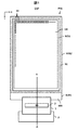
- FIG. 1 is a plan view of a display device to which the present invention is applied.
- FIG. 2 is a sectional view taken along line AA of FIG.
- the display device DSP includes a display panel PNL, a flexible printed circuit board 1, an IC chip 2, and a circuit board 3.
- the display panel PNL is a liquid crystal display panel, and includes a first substrate (also referred to as a TFT substrate or an array substrate) SUB1, a second substrate (also referred to as a counter substrate) SUB2, a liquid crystal layer LC, and a sealing material SE. ing.
- the display panel PNL includes a display section (display area) DA for displaying an image, and a frame-shaped non-display section (non-display area) NDA surrounding the outer periphery of the display section DA.
- the second substrate SUB2 faces the first substrate SUB1.
- the first substrate SUB1 has a mounting portion MA extending in the second direction Y from the second substrate SUB2.
- the sealing material SE is located in the non-display portion NDA, and bonds the first substrate SUB1 and the second substrate SUB2 and seals the liquid crystal layer LC.
- lower polarizing plate 200 is attached below first substrate SUB1, and upper polarizing plate 201 is attached above second substrate SUB2.
- the combination of the first substrate SUB1, the second substrate SUB2, the lower polarizing plate 200, the upper polarizing plate 201, and the liquid crystal layer LC is called a display panel PNL. Since the display panel PNL does not emit light by itself, the backlight 202 is disposed below (backside) the display panel PNL.
- a plurality of external terminals are formed in the mounting part MA.
- the flexible printed circuit board 1 is connected to a plurality of external terminals of the mounting part MA.
- An IC chip 2 for supplying a video signal and the like is mounted on the flexible printed circuit board 1.
- the flexible printed circuit board 1 is connected to a circuit board 3 for externally supplying signals and power to the IC chip 2 and the display device DSP. Note that the IC chip 2 may be mounted on the mounting section MA.
- the IC chip 2 has a built-in display driver DD that outputs a signal necessary for image display in a display mode for displaying an image.
- a plurality of pixels PX are formed in a matrix in the display area DA, and each pixel PX has a thin film transistor (TFT: Thin Film Transistor) as a switching element.
- TFT Thin Film Transistor
- a driving circuit for controlling and driving a scanning line, a video signal line (hereinafter, referred to as a signal line) and the like is formed.
- the drive circuit has a thin film transistor (TFT).
- the TFT used as the switching element of the pixel PX needs to have a small leak current.
- a TFT using an oxide semiconductor can reduce leakage current.
- the oxide semiconductor is referred to as an OS (Oxide @ Semiconductor).
- the OS includes IGZO (Indium Galium Zinc Oxide), ITZO (Indium Tin Zinc Oxide), ZnON (Zinc Oxide Nitride), and IGO (Indium Galium Oxide).
- an oxide semiconductor will be described using an OS as a representative. Since the OS has low carrier mobility, it may be difficult to form a driver circuit built in the display device DSP using a TFT using the OS.
- OS is also used in the meaning of TFT using OS.
- LTPS Low Temperature, Poly-Si
- LTPS Low Temperature, Poly-Si
- the driver circuit can be formed using a thin film transistor (TFT) using LTPS.
- TFT thin film transistor
- LTPS is also used in the meaning of TFT using LTPS.
- the thin film transistor (TFT) used for the pixel PX needs to have a small leak current, an oxide semiconductor (OS) is used, and the thin film transistor (TFT) used for the driver circuit needs to have high mobility. As such, it is reasonable to use LTPS.
- OS oxide semiconductor
- TFT thin film transistor
- the design of the present invention is effective even when a-Si or OS is used for the drive circuit, since the design can be made even with the mobility of amorphous silicon (a-Si) or OS depending on the applied product. is there.
- the display panel PNL of the present embodiment is a transmissive type having a transmissive display function of displaying an image by selectively transmitting light from the back side of the first substrate SUB1, and light from the front side of the second substrate SUB2.
- a transmissive type having a transmissive display function of displaying an image by selectively transmitting light from the back side of the first substrate SUB1, and light from the front side of the second substrate SUB2.
- the display panel PNL is also provided with a display mode using a vertical electric field along a normal line of the substrate main surface, and a display mode oblique to the substrate main surface.
- a display mode using a vertical electric field along a normal line of the substrate main surface and a display mode oblique to the substrate main surface.
- Any configuration corresponding to a display mode using an inclined electric field inclined in a direction and a display mode using an appropriate combination of the above-described horizontal electric field, vertical electric field, and inclined electric field may be provided.
- the substrate main surface is a surface parallel to the XY plane defined by the first direction X and the second direction Y.
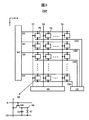
- FIG. 3 is a diagram illustrating a basic configuration of the pixel PX and an equivalent circuit of the display device DSP.
- the plurality of pixels PX are arranged in a matrix in the first direction X and the second direction Y.
- the plurality of scanning lines G (G1, G2,...) Are connected to a scanning line driving circuit GD.
- the plurality of signal lines S (S1, S2,%) are connected to a signal line driving circuit SD.
- the plurality of common electrodes CE CE1, CE2,...) are connected to a voltage supply unit CD for a common voltage (Vcom), and are arranged over a plurality of pixels PX.
- One pixel PX is connected to one scanning line, one signal line, and one common electrode CE.
- the scanning lines G and the signal lines S do not necessarily have to extend linearly, and some of them may be bent. For example, it is assumed that the signal line S extends in the second direction Y even if a part thereof is bent.
- the scanning line driving circuit GD, the signal line driving circuit SD, and the voltage supply unit CD are configured by thin film transistors (TFTs).
- Each pixel PX includes a switching element SW, a pixel electrode PE, a common electrode CE, a liquid crystal layer LC, and the like.
- the switching element SW is composed of, for example, a thin film transistor (TFT), and is electrically connected to the scanning line G and the signal line S.
- the scanning line G is connected to the switching element SW in each of the pixels PX arranged in the first direction X.
- the signal line S is connected to the switching element SW in each of the pixels PX arranged in the second direction Y.
- the pixel electrode PE is electrically connected to the switching element SW.
- Each of the pixel electrodes PE faces the common electrode CE, and drives the liquid crystal layer LC by an electric field generated between the pixel electrode PE and the common electrode CE.
- the storage capacitor CS is formed, for example, between an electrode having the same potential as the common electrode CE and between an electrode having the same potential as the pixel electrode PE.
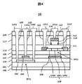
- FIG. 4 is a cross-sectional view illustrating the configuration of the semiconductor device according to the embodiment.
- the semiconductor device 10 shown in FIG. 4 is a first substrate SUB1 including a plurality of thin film transistors TFT1 and TFT2.
- a thin film transistor (first thin film transistor) TFT1 on the left is a thin film transistor (LTPSTFT) using LTPS
- a thin film transistor (second thin film transistor) TFT2 on the right is a thin film transistor (OSFT) using an oxide semiconductor (OS).
- the semiconductor device 10 is a semiconductor device built in the display panel PNL.
- the semiconductor device 10 includes a substrate 100, a base film 101, a first semiconductor layer 102, a first gate insulating film 104, a first gate electrode 105, a light shielding layer 106, a first insulating film 107, a second insulating film 108, and a second semiconductor.
- a layer 109, a second gate insulating film 112, an aluminum oxide film (AlO film) 113, a second gate electrode 116, a third insulating film 117, a fourth insulating film 118, and the like are provided.
- AlO film 113 is an example, and is not limited to this.
- the AlO film can be changed to an oxide semiconductor film containing much oxygen.
- the AlO film 113 is a film used for supplying oxygen to the channel region 1091 of the second semiconductor layer 109, as described later. That is, since the film 113 may be any means (film or layer) capable of supplying oxygen to the channel region of the oxide semiconductor, an AlO film or an oxide semiconductor film containing a large amount of oxygen (OS) is used. can do.
- an AlO film will be described as a representative example.
- a base film 101 is formed on a substrate 100 made of glass or resin.
- the base film 101 blocks impurities from glass or the like, and is usually formed of silicon oxide SiO or silicon nitride SiN by CVD.
- AB eg, SiO
- the notation of AB (eg, SiO) or the like in the present specification indicates that the compound has A and B as constituent elements, and means that A and B have the same composition ratio. Not.
- a first semiconductor layer 102 for LTPS TFT is formed.
- the first semiconductor layer 102 is formed by LTPS.
- a first gate insulating film 104 is formed to cover the first semiconductor layer 102.
- a-Si amorphous silicon
- the first semiconductor layer 102 is annealed for dehydrogenation, and then irradiated with excimer laser to convert a-Si into polycrystalline silicon (Poly-Si). Si), and then it is possible to form Poly-Si by patterning.
- the first gate insulating film 104 can be formed of SiO using TEOS (tetraethyl orthosilicate) as a raw material.
- the first gate electrode 105 and the light shielding layer 106 are formed on the first gate insulating film 104.
- the first gate electrode 105 and the light-shielding layer 106 are formed of a laminated film of Ti—Al alloy—Ti or the like, or a MoW alloy or the like.
- the light-blocking layer 106 blocks light so that light from the backlight 202 is not irradiated to the channel region 1091 of the OSTFT.
- the first insulating film 107 is formed to cover the first gate electrode 105, the light shielding layer 106, and the first gate insulating film 104.
- the first insulating film 107 is formed of SiN by CVD.
- a second insulating film 108 is formed on the first insulating film 107.
- the second insulating film 108 is formed of SiO by CVD.
- the second semiconductor layer 109 for the OSTFT is formed on the second insulating film 108.
- the second semiconductor layer 109 is formed of an OS.
- the second semiconductor layer 109 includes a channel region 1091, a drain region 1092, and a source region 1093.
- the channel region 1091 is provided between the drain region 1092 and the source region 1093. Therefore, the thin film transistor TFT2 is located above the thin film transistor TFT1 when viewed from the substrate 100.
- a protective metal layer 111 is provided at one end and the other end of the second semiconductor layer 109. That is, the metal layer 111 is connected to the end of the drain region 1092 not in contact with the channel region 1091 and the end of the source region 1093 not in contact with the channel region 1091.
- Metal layer 111 is formed of, for example, titanium (Ti).
- a second gate insulating film 112 is formed to cover the second insulating film 108, the second semiconductor layer 109, and the metal layer 111.
- the second gate insulating film 112 can be formed of SiO by CVD using SiH4 (silane) and N2O (nitrous oxide).
- an aluminum oxide film (hereinafter, represented by AlO) 113 is formed on the second gate insulating film 112 corresponding to the channel region 1091.
- AlO aluminum oxide film
- a block layer 114 is formed on the AlO film 113.
- a second gate electrode 116 is formed on the AlO film 113. Therefore, the AlO film 113 is selectively provided below the second gate electrode 116.
- the AlO film 113 and the second gate electrode 116 are provided in an island shape when the entire semiconductor device 10 is viewed in a plan view.
- the second gate electrode 116 is formed of, for example, a laminated film of Ti—Al alloy—Ti or a MoW alloy.
- the AlO film 113 is provided in a portion corresponding to the lower side of the second gate electrode 116, and is also formed in a portion above the channel region 1091.
- the AlO film 113 has a role of supplying oxygen to the channel region 1091 of the second semiconductor layer 109. Oxygen is supplied to the channel region 1091 from the AlO film 113 located between the two block layers 114.
- the block layer 114 is used for preventing oxygen from entering the drain region 1092 and the source region 1093.
- the block layer 114 can be formed using OS having a low oxygen concentration or SiN. As described above, as the AlO film 113, an oxide semiconductor film containing much oxygen can be used.
- a third insulating film 117 is formed to cover the second gate insulating film 112, the second gate electrode 116, the AlO film 113, and the block layer 114.
- the third insulating film 117 is formed of SiN.
- a fourth insulating film 118 is formed on the third insulating film 117.
- the fourth insulating film 118 is formed of SiO.
- a contact hole 120 for forming a gate electrode wiring 1191 and a source / drain electrode wiring 1192 in the LTPS TFT and a contact hole 122 for forming a gate electrode wiring 1211 and a source / drain electrode wiring 1212 in the OSTFT are formed.
- the contact holes 120 and 122 are formed by, for example, dry etching using a CF (eg, CF4) or CHF (eg, CHF3) gas.
- CF eg, CF4
- CHF eg, CHF3
- a gate electrode wiring 1191, a source / drain electrode wiring 1192, a gate electrode wiring 1211 and a source / drain electrode wiring 1212 are formed.
- the source / drain electrode wiring (1192, 1212) is a source / drain electrode wiring (1192, 1212) including the source electrode wiring and the drain electrode wiring.
- the gate electrode wirings 1191 and 1211 and the source / drain electrode wirings 1192 and 1212 can be formed of, for example, a stacked film of Ti, an Al alloy, Ti, or the like.
- contact is made with five layers of insulating films (118, 117, 112, 108, 107) and six layers of insulating films (118, 117, 112, 108, 107, 104).
- contact holes 122 are formed in the two insulating films (118, 117) and the three insulating films (118, 117, 112), whereas the holes 120 are formed. Therefore, it is necessary to adjust the etching conditions for forming the contact hole to the LTPS TFT side. In other words, although the OSTFT side is exposed to the etching gas and the cleaning liquid for a longer time, the provision of the protective metal layer 111 prevents the second semiconductor layer 109 from disappearing, so that the OSTFT can be formed stably.
- the drain region 1092 and the source region 1093 of the second semiconductor layer 109 have low resistance because the supply of oxygen from the AlO film 113 is suppressed by the block layer 114. Therefore, an OSTFT having good transistor characteristics can be realized. Further, a semiconductor device such as a display device using an OSTFT having favorable transistor characteristics can be realized.
- both ends of the channel region 1091 are made to have high resistance, so that the current of the OSTFT flows. This makes it possible to realize an OSTFT having good switching characteristics.
- FIG. 5 shows that a base film 101 is formed on an insulating substrate 100, a first semiconductor layer 102 is formed thereon, a first gate insulating film 104 is formed over the base film 101, and a first gate insulating film 104 is formed thereon.
- FIG. 3 is a cross-sectional view showing a state where a gate electrode 105 and a light shielding layer 106 are formed.
- the first semiconductor layer 102 is doped with B (boron) or P (phosphorus) by ion implantation using the first gate electrode 105 as a mask.
- B boron
- P phosphorus
- FIG. 6 is a cross-sectional view showing a state in which the first insulating film 107 is formed so as to cover the first gate electrode 105, the light shielding layer 106, and the first gate insulating film 104.
- the first insulating film 107 is formed of SiN by CVD.
- FIG. 7 is a cross-sectional view showing a state in which the second insulating film 108 is formed on the first insulating film 107, and the second semiconductor layer 109 is selectively formed on the second insulating film 108.
- the second insulating film 108 is formed of SiO by CVD.
- the second semiconductor layer 109 is formed of an OS.
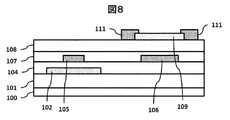
- FIG. 8 is a cross-sectional view showing a state in which protective metal layers 111 are selectively formed at both ends of the second semiconductor layer 109.
- Metal layer 111 is formed of, for example, Ti. As described with reference to FIG. 4, the metal layer 111 is a protective film for preventing the disappearance of the second semiconductor layer 109 due to an etching gas and a cleaning solution when forming the contact holes (120, 122).
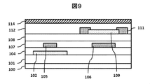
- FIG. 9 shows a state in which a second gate insulating film 112 is formed to cover the second insulating film 108, the second semiconductor layer 109, and the metal layer 111, and a block layer 114 is formed on the second gate insulating film 112. It is sectional drawing.
- the second gate insulating film 112 can be formed of SiO by CVD using SiH4 (silane) and N2O (nitrous oxide).
- the block layer 114 can be formed using OS having a low oxygen concentration or SiN.
- the thickness of the block layer 114 is, for example, about 10 nm to 30 nm.
- FIG. 10 is a cross-sectional view showing a state where the block layer 114 is selectively patterned.
- the block layer 114 is selectively patterned so as to have an opening covering the upper side of the channel region (1091) of the second semiconductor layer 109 in a cross-sectional view and a plan view.
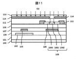
- FIG. 11 is a cross-sectional view showing a state in which an AlO film 113 is formed on the block layer 114 and the second gate insulating film 112 exposed from the opening of the block layer 114.
- the AlO film 113 is formed by reactive sputtering, it contains a large amount of oxygen. This oxygen stabilizes the insulation resistance of the channel region 1091 of the second semiconductor layer 109. That is, oxygen O2 at the time of forming the AlO film 113 is blocked by the block layer 114, but a large amount of oxygen is introduced into the channel region 1091 of the second semiconductor layer 109 where the block layer 114 is not provided. Therefore, the channel region 1091 is hyperoxygenated and has high resistance.
- the supply of oxygen to the drain region 1092 and the source region 1093 of the second semiconductor layer 109 is restricted by the block layer 114, so that the region is not over-oxygenated and easily maintained at a low resistance.
- a channel region 1091, a drain region 1092, and a source region 1093 are referred to as regions where channel regions, drain regions, and source regions are to be formed for the purpose of simplifying the description. Are also described as a channel region 1091, a drain region 1092, and a source region 1093.
- FIG. 12 is a cross-sectional view showing a state where the second gate electrode 116 is formed on the AlO film 113.
- the second gate electrode 116 is formed of, for example, a laminated film of Ti—Al alloy—Ti or a MoW alloy.
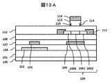
- FIG. 13A is a cross-sectional view showing a state where the block layer 114, the AlO film 113, and the second gate electrode 116 are selectively patterned.
- FIG. 13B is a plan view when the state shown in FIG. 13A is viewed from above.
- the block layer 114, the AlO film 113, and the second gate electrode 116 are selectively patterned so as to cover the upper side of the channel region (1091) of the second semiconductor layer 109.
- the AlO film 113 is selectively provided below the second gate electrode 116. Therefore, when the semiconductor device 10 is viewed as a whole in plan view, the AlO film 113 and the second gate electrode 116 are provided in an island shape.
- ion implantation is performed using the second gate electrode 116 as a mask to impart conductivity to the second semiconductor layer 109 other than the portion covered with the second gate electrode 116.
- ion implantation is effectively performed in a region where the AlO film 113 and the block layer 114 do not cover the drain region 1092 and the source region 1093.
- B boron
- P phosphorus
- Ar argon
- a conductive drain region 1092 and a source region 1093 are formed in the second semiconductor layer 109 by ion implantation.
- an activation process is performed in a hydrogen atmosphere to reduce the resistance of the drain region 1092 and the source region 1093. Therefore, a thin film transistor using an oxide semiconductor (OS) with stable characteristics can be realized.
- OS oxide semiconductor
- FIG. 14 shows that the third insulating film 117 is formed so as to cover the second gate insulating film 112, the selectively patterned block layer 114, the AlO film 113, and the second gate electrode 116.
- FIG. 14 is a cross-sectional view showing a state where a fourth insulating film 118 is formed thereon.
- the third insulating film 117 is formed of SiN by CVD.
- the fourth insulating film 118 is formed of SiO by CVD.
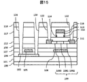
- FIG. 15 is a cross-sectional view showing a state where contact holes 120 and 122 are formed.
- the contact holes 120 and 122 are formed by, for example, dry etching using a CF (eg, CF4) or CHF (eg, CHF3) gas.
- the contact holes 120 and 122 can be formed simultaneously.
- a contact hole 120 is formed in the six-layer insulating film (118, 117, 112, 108, 107, 104) so that the drain region and the source region of the first semiconductor layer 102 are exposed.
- a contact hole 122 is formed in the three-layer insulating film (118, 117, 112) so that the metal layer 111 is exposed. Thereafter, the contact holes 120 and 122 are cleaned with an HF-based cleaning solution.
- FIG. 16 is a cross-sectional view showing a state in which source / drain electrode wirings 1192 and 1212 are formed in contact holes 120 and 122. After cleaning the contact holes 120 and 122, source / drain electrode wirings 1192 and 1212 are formed in the contact holes 120 and 122. That is, the source / drain electrode wiring 1192 is formed in the contact hole 120 on the LTPS TFT side. On the OSTFT side, a source / drain electrode wiring 1212 is formed in the contact hole 122.
- FIG. 15 and FIG. 16 do not show the gate electrode wires 1191 and 1211 shown in FIG. 4, but the gate electrode wires 1191 and 1211 may be formed as described in FIG.
- a contact hole 120 is formed in five layers of insulating films (118, 117, 112, 108, 107) so that the first gate electrode 105 is exposed, and a gate electrode wiring 1191 is formed in the contact hole 120.
- a contact hole 122 is formed in the two-layer insulating film (118, 117) so that the second gate electrode 116 is exposed, and a gate electrode wiring 1211 is formed in the contact hole 122.
- the semiconductor device 10 such as a display device including the LTPS TFT and the OSTFT has been described.
- a semiconductor device 10a such as a display device having only an OSTFT will be described.
- the protective metal layer 111 connected to the drain region 1092 and the source region 1093 can be omitted. Therefore, the steps of forming and patterning the metal layer 111 and the step of cleaning the contact holes can be omitted, so that the manufacturing steps can be shortened.
- FIGS. 17 to 23 are cross-sectional views showing manufacturing steps of a semiconductor device 10a according to a modification.
- the semiconductor device 10a is a first substrate SUB1 including a thin film transistor TFT2 (OSTFT) using an oxide semiconductor (OS).
- the semiconductor device 10a is a semiconductor device built in a display panel.
- a method of manufacturing the semiconductor device 10a according to the modification will be described with reference to FIGS.
- FIG. 17 shows that a base film 101 is formed over an insulating substrate 100, a semiconductor layer 109a is formed over the base film 101, and a gate insulating film 301 is formed to cover the base film 101 and the semiconductor layer 109a.
- FIG. 4 is a cross-sectional view showing a state where a block layer 302 is formed on a gate insulating film 301.
- the substrate 100 is formed of glass or resin.
- the base film 101 is formed of silicon oxide SiO or silicon nitride SiN by CVD.
- the semiconductor layer 109a is formed using an OS.
- the gate insulating film 301 can be formed of SiO by CVD using SiH4 (silane) and N2O (nitrous oxide).
- the block layer 302 can be formed using an oxide semiconductor (OS) having a low oxygen concentration or SiN.
- the thickness of the block layer 302 is, for example, about 10 nm to 30 nm.
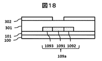
- FIG. 18 is a cross-sectional view showing a state where the block layer 302 is selectively patterned.
- the block layer 302 is selectively patterned so as to have an opening covering the upper side of the channel region (1091) of the semiconductor layer 109a in a sectional view and a plan view.
- FIG. 19 is a cross-sectional view showing a state in which an AlO film 303 is formed on the block layer 302 and the gate insulating film 301 exposed from the opening of the block layer 302.
- the AlO film 303 contains a large amount of oxygen because it is formed by reactive sputtering. This oxygen stabilizes the insulation resistance of the channel region 1091 of the semiconductor layer 109a. That is, oxygen O2 at the time of forming the AlO film 303 is blocked by the block layer 302, but a large amount of oxygen is supplied to the channel region 1091 of the semiconductor layer 109a where the block layer 302 is not provided.
- the channel region 1091 is hyperoxygenated and has high resistance.
- the supply of oxygen to the drain region 1092 and the source region 1093 of the semiconductor layer 109a is limited by the block layer 302, so that the region is not over-oxygenated and low resistance is easily maintained.
- the AlO film 303 can be changed to an oxide semiconductor film containing much oxygen. That is, the film 303 may be any means (film or layer) capable of supplying oxygen to the channel region of the semiconductor layer 109a; therefore, an AlO film or an oxide semiconductor film containing much oxygen can be used. it can.
- the AlO film will be described as a representative example.
- FIG. 20 is a cross-sectional view showing a state in which a gate electrode 304 is formed on an AlO film 303.
- the gate electrode 304 is formed of, for example, a laminated film of Ti—Al alloy—Ti or a MoW alloy.
- FIG. 21 is a cross-sectional view showing a state where the block layer 302, the AlO film 303, and the gate electrode 304 are selectively patterned.
- the block layer 302, the AlO film 303, and the gate electrode 304 are selectively patterned so as to cover the upper side of the channel region (1091) of the semiconductor layer 109a.
- the AlO film 303 is provided below the gate electrode 304.
- the AlO film 303 and the gate electrode 304 are formed in an island shape when the entire semiconductor device 10a is viewed in a plan view.
- ion implantation is performed using the gate electrode 304 as a mask to impart conductivity to the semiconductor layer 109a other than the portion covered with the gate electrode 304.
- boron, P (phosphorus), Ar (argon), or the like is used as ions for ion implantation.
- a conductive drain region 1092 and a source region 1093 are formed in the semiconductor layer 109a.
- an activation process is performed in a hydrogen atmosphere to reduce the resistance of the drain region 1092 and the source region 1093. Therefore, a thin film transistor using an oxide semiconductor (OS) with stable characteristics can be realized.
- OS oxide semiconductor
- FIG. 22 shows that a first insulating film 305 is formed to cover a gate insulating film 301, a selectively patterned block layer 302, an AlO film 303, and a gate electrode 304, and a second insulating film 305 is formed on the first insulating film 305.
- FIG. 4 is a cross-sectional view showing a state where an insulating film 306 is formed.
- the first insulating film 305 is formed of SiN by CVD.
- the second insulating film 306 is formed of SiO by CVD.
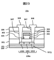
- FIG. 23 is a cross-sectional view showing a state where the source / drain electrode wiring 308 is formed in the contact hole 307.
- the contact hole 307 is formed by, for example, dry etching using a CF (for example, CF4) or CHF (for example, CHF3) gas.
- the contact hole 307 is formed in the three-layer insulating film (306, 305, 301) such that the drain region 1092 and the source region 1093 are exposed.
- a source / drain electrode wiring 308 is formed in the contact hole 307.
- a semiconductor device 10a according to a modification including the thin film transistor TFT2 (OSTFT) using an oxide semiconductor (OS) is formed.
- OSTFT thin film transistor TFT2
- OS oxide semiconductor
- the manufacturing process can be shortened by configuring the OSTFT.
- sufficient oxygen is supplied from the AlO film 303 to the channel region 1091 of the semiconductor layer 109a to increase the resistance.
- the block layer 302 is formed on the drain region 1092 and the source region 1093 of the semiconductor layer 109a as shown in FIGS. 18 and 19, oxygen from the AlO film 303 is blocked, and the drain region 1092 is formed.
- the resistance of the source region 1093 is reduced. Therefore, an OSTFT having good transistor characteristics can be realized. Further, a semiconductor device 10a such as a display device using an OSTFT having good transistor characteristics can be realized.
- both ends of the channel region 1091 are made to have high resistance, so that the current of the OSTFT flows. This makes it possible to realize an OSTFT having good switching characteristics.
- ⁇ ⁇ Various inventions can be formed by appropriately combining a plurality of components disclosed in the above embodiments. For example, some components may be deleted from all the components shown in the embodiment. Further, components of different embodiments may be appropriately combined.
- DSP display device
- PNL display panel
- DA display area
- NDA non-display area
- SUB1 first substrate (array substrate)
- SUB2 second substrate (counter substrate)
- SE sealing material
- LC liquid crystal layer
- MA mounting portion
- PX pixel
- TFT1 thin film transistor
- TFT2 thin film transistor
- 1 flexible printed circuit board
- 2 IC chip
- 3 circuit board
- 10 semiconductor device, 100: substrate, 101: base film, # 102: first semiconductor layer, # 104: first gate insulating film, # 105: first gate electrode, # 106: light shielding layer, # 107: first insulating film, # 108: second insulating film, # 109: second Semiconductor layer, # 111: metal layer, # 112: second gate insulating film, # 113: AlO film, # 1 4: Block layer, 116: second gate electrode, 117: third insulating film, 118: fourth insulating film
Landscapes
- Physics & Mathematics (AREA)
- Nonlinear Science (AREA)
- General Physics & Mathematics (AREA)
- Engineering & Computer Science (AREA)
- Chemical & Material Sciences (AREA)
- Crystallography & Structural Chemistry (AREA)
- Mathematical Physics (AREA)
- Microelectronics & Electronic Packaging (AREA)
- Optics & Photonics (AREA)
- Theoretical Computer Science (AREA)
- Liquid Crystal (AREA)
- Thin Film Transistor (AREA)
- Devices For Indicating Variable Information By Combining Individual Elements (AREA)
- Metal-Oxide And Bipolar Metal-Oxide Semiconductor Integrated Circuits (AREA)
Abstract
本開示の目的は、酸化物半導体を用いた薄膜トランジスタにおいて、酸化物半導体のチャネル領域を高抵抗化させるとともに、酸化物半導体のソース領域およびドレイン領域を低抵抗化させる技術を提供することにある。酸化物半導体を有する薄膜トランジスタを備え、前記酸化物半導体は、チャネル領域と、ドレイン領域と、ソース領域と、を有し、前記チャネル領域の上に設けられたゲート絶縁膜と、前記ゲート絶縁膜の上に設けられたアルミニウム酸化膜と、前記アルミニウム酸化膜の上に設けられたゲート電極と、を有し、前記アルミニウム酸化膜は、平面視において、前記ドレイン領域および前記ソース領域のいずれに対しても覆わない領域を有する半導体装置が提供される。
Description
本発明は半導体装置に関し、特に、酸化物半導体を用いた薄膜トランジスタを有する表示装置等の半導体装置に関する。
液晶表示装置では画素電極および薄膜トランジスタ(TFT:Thin Film Transistor)等を有する画素がマトリクス状に形成されたTFT基板と、TFT基板に対向して対向基板が配置され、TFT基板と対向基板の間に液晶が挟持されている構成となっている。そして液晶分子による光の透過率を画素毎に制御することによって画像を形成している。
酸化物半導体を用いたTFTはリーク電流が小さいので、画素領域におけるスイッチングTFTとして好適である。
画素領域におけるスイッチングTFTは、リーク電流が小さいことが必要である。一方、画素領域におけるスイッチングTFTは、ON電流は大きいことが要求されている。すなわち、酸化物半導体を用いたTFTにおいて、チャネル領域では十分に大きな抵抗を維持し、ソース領域、ドレイン領域では抵抗が十分に小さい必要がある。
特開2017-107913号公報(特許文献1)には、「絶縁基板上に、酸素を含む島状の第1の絶縁層を形成し、第1の絶縁層に酸素イオンを注入し、絶縁基板及び第1の絶縁層上に酸化物半導体層を形成し、熱処理により第1の絶縁層から半導体層の第1の絶縁層上の領域に酸素を供給し、チャネル領域を形成する」という薄膜トランジスタの製造方法が提案されている。
本発明者らは、酸化物半導体を用いたTFTの製造において、酸化物半導体上にゲート絶縁膜を形成し、そのゲート絶縁膜と積層してアルミニウム酸化膜を形成し、アルミニウム酸化膜の成膜時に、ゲート絶縁膜の全面に酸素を供給することで、酸化物半導体のチャネル領域に酸素を供給する方法を検討した。しかしながら、この方法では、チャネル領に隣接する酸化物半導体のソース領域およびドレイン領域にも、酸素が供給され、低抵抗化することが難しいことがわかった。
本発明は、酸化物半導体のチャネル領域に酸素を供給する手段(アルミニウム酸化膜)が酸化物半導体のドレイン領域およびソース領域に影響を与え、ドレイン領域、ソース領域の抵抗が大きくなって、ON電流が小さくなる現象を対策するものである。
本発明の目的は、酸化物半導体を用いた薄膜トランジスタにおいて、酸化物半導体のチャネル領域を高抵抗化させるとともに、酸化物半導体のソース領域およびドレイン領域を低抵抗化させる技術を提供することにある。
その他の課題と新規な特徴は、本明細書の記述および添付図面から明らかになるであろう。
本発明のうち代表的なものの概要を簡単に説明すれば下記の通りである。
本実施形態の一態様によれば、
酸化物半導体を有する薄膜トランジスタを備え、前記酸化物半導体は、チャネル領域と、ドレイン領域と、ソース領域と、を有し、前記チャネル領域の上に設けられたゲート絶縁膜と、前記ゲート絶縁膜の上に設けられたアルミニウム酸化膜と、前記アルミニウム酸化膜の上に設けられたゲート電極と、を有し、前記アルミニウム酸化膜は、平面視において、前記ドレイン領域および前記ソース領域のいずれに対しても覆わない領域を有する半導体装置が提供される。
酸化物半導体を有する薄膜トランジスタを備え、前記酸化物半導体は、チャネル領域と、ドレイン領域と、ソース領域と、を有し、前記チャネル領域の上に設けられたゲート絶縁膜と、前記ゲート絶縁膜の上に設けられたアルミニウム酸化膜と、前記アルミニウム酸化膜の上に設けられたゲート電極と、を有し、前記アルミニウム酸化膜は、平面視において、前記ドレイン領域および前記ソース領域のいずれに対しても覆わない領域を有する半導体装置が提供される。
また、本実施形態の他の一態様によれば、
基板と、前記基板の上に設けられ、多結晶シリコンで構成された第1薄膜トランジスタと、前記基板の上に設けられ、酸化物半導体で構成された第2薄膜トランジスタと、を含み、前記酸化物半導体は、チャネル領域と、ドレイン領域と、ソース領域と、を有し、前記チャネル領域の上に設けられたゲート絶縁膜と、前記ゲート絶縁膜の上に設けられたアルミニウム酸化膜と、前記アルミニウム酸化膜の上に設けられたゲート電極と、を含む、半導体装置が提供される。
基板と、前記基板の上に設けられ、多結晶シリコンで構成された第1薄膜トランジスタと、前記基板の上に設けられ、酸化物半導体で構成された第2薄膜トランジスタと、を含み、前記酸化物半導体は、チャネル領域と、ドレイン領域と、ソース領域と、を有し、前記チャネル領域の上に設けられたゲート絶縁膜と、前記ゲート絶縁膜の上に設けられたアルミニウム酸化膜と、前記アルミニウム酸化膜の上に設けられたゲート電極と、を含む、半導体装置が提供される。
また、本実施形態のさらに他の一態様によれば、
チャネル領域とドレイン領域とソース領域とを有する酸化物半導体の半導体層で構成された薄膜トランジスタを含む半導体装置の製造方法であって、基板の上に、前記半導体層を形成する工程と、前記半導体層を覆う様に、ゲート絶縁膜を形成する工程と、前記ゲート絶縁膜の上に、前記半導体層の前記チャネル領域の上方に開口部を有するブロック層を形成する工程と、前記ブロック層の上、および、前記開口部から露出する前記ゲート絶縁膜の上に、アルミニウム酸化膜を形成するとともに、前記開口部から前記半導体層の前記チャネル領域へ酸素を供給する工程と、を含む、半導体装置の製造方法が提供される。
チャネル領域とドレイン領域とソース領域とを有する酸化物半導体の半導体層で構成された薄膜トランジスタを含む半導体装置の製造方法であって、基板の上に、前記半導体層を形成する工程と、前記半導体層を覆う様に、ゲート絶縁膜を形成する工程と、前記ゲート絶縁膜の上に、前記半導体層の前記チャネル領域の上方に開口部を有するブロック層を形成する工程と、前記ブロック層の上、および、前記開口部から露出する前記ゲート絶縁膜の上に、アルミニウム酸化膜を形成するとともに、前記開口部から前記半導体層の前記チャネル領域へ酸素を供給する工程と、を含む、半導体装置の製造方法が提供される。
以下に、本発明の各実施の形態について、図面を参照しつつ説明する。
なお、開示はあくまで一例にすぎず、当業者において、発明の主旨を保っての適宜変更について容易に想到し得るものについては、当然に本発明の範囲に含有されるものである。また、図面は説明をより明確にするため、実際の態様に比べ、各部の幅、厚さ、形状等について模式的に表される場合があるが、あくまで一例であって、本発明の解釈を限定するものではない。また、本明細書と各図において、既出の図に関して前述したものと同様の要素には、同一の符号を付して、詳細な説明を適宜省略することがある。
本実施形態においては、表示装置の一例として、液晶表示装置を開示する。この液晶表示装置は、例えば、スマートフォン、タブレット端末、携帯電話端末、パーソナルコンピュータ、テレビ受像装置、車載装置、ゲーム機器等の種々の装置に用いることができる。
なお、本明細書及び請求の範囲において、図面を説明する際の「上」、「下」などの表現は、着目する構造体と他の構造体との相対的な位置関係を表現している。具体的には、側面から見た場合において、第1基板(アレイ基板)から第2基板(対向基板)に向かう方向を「上」と定義し、その逆の方向を「下」と定義する。
また、「内側」及び「外側」とは、2つの部位における、表示領域を基準とした相対的な位置関係を示す。すなわち、「内側」とは、一方の部位に対し相対的に表示領域に近い側を指し、「外側」とは、一方の部位に対し相対的に表示領域から遠い側を指す。ただし、ここで言う「内側」及び「外側」の定義は、液晶表示装置を折り曲げていない状態におけるものとする。
「表示装置」とは、表示パネルを用いて映像を表示する表示装置全般を指す。「表示パネル」とは、電気光学層を用いて映像を表示する構造体を指す。例えば、表示パネルという用語は、電気光学層を含む表示セルを指す場合もあるし、表示セルに対して他の光学部材(例えば、偏光部材、バックライト、タッチパネル等)を装着した構造体を指す場合もある。ここで、「電気光学層」には、技術的な矛盾を生じない限り、液晶層、エレクトロクロミック(EC)層などが含まれ得る。したがって、後述する実施形態について、表示パネルとして、液晶層を含む液晶パネルを例示して説明するが、上述した他の電気光学層を含む表示パネルへの適用を排除するものではない。
(表示装置の全体構成例)
図1は、本発明が適用される表示装置の平面図である。図2は、図1のA-A線に沿う断面図である。
図1は、本発明が適用される表示装置の平面図である。図2は、図1のA-A線に沿う断面図である。
図1および図2において、表示装置DSPは、表示パネルPNLと、フレキシブルプリント回路基板1と、ICチップ2と、回路基板3と、を備えている。表示パネルPNLは、液晶表示パネルであり、第1基板(TFT基板、アレイ基板ともいう)SUB1と、第2基板(対向基板ともいう)SUB2と、液晶層LCと、シール材SEと、を備えている。
表示パネルPNLは、画像を表示する表示部(表示領域)DAと、表示部DAの外周を囲む額縁状の非表示部(非表示領域)NDAと、を備えている。第2基板SUB2は、第1基板SUB1に対向している。第1基板SUB1は、第2基板SUB2よりも第2方向Yに延出した実装部MAを有している。シール材SEは、非表示部NDAに位置し、第1基板SUB1と第2基板SUB2とを接着するとともに、液晶層LCを封止している。
図2を参照し、第1基板SUB1の下には下偏光板200が貼り付けられ、第2基板SUB2の上側には上偏光板201が貼り付けられている。第1基板SUB1、第2基板SUB2、下偏光板200、上偏光板201、液晶層LCの組み合わせを表示パネルPNLと呼ぶ。表示パネルPNLは自身では発光しないので、表示パネルPNLの下(背面)にバックライト202が配置されている。
実装部MAには、複数の外部端子が形成されている。実装部MAの複数の外部端子には、フレキシブルプリント回路基板1が接続される。フレキシブルプリント回路基板1には、映像信号等を供給するICチップ2が搭載されている。フレキシブルプリント回路基板1には、ICチップ2や表示装置DSPに外部から信号や電力を供給するための回路基板3が接続されている。なお、ICチップ2は、実装部MAに実装されてもよい。ICチップ2は、画像を表示する表示モードにおいて画像表示に必要な信号を出力するディスプレイドライバDDを内蔵している。
図1に示すように、表示領域DAには、複数の画素PXがマトリクス状に形成され、各画素PXはスイッチング素子として薄膜トランジスタ(TFT:Thin Film Transistor)を有している。非表示領域NDAには、走査線、映像信号線(以下、信号線という)等を制御および駆動するための、駆動回路が形成されている。駆動回路は、薄膜トランジスタ(TFT)を有している。
画素PXのスイッチング素子として用いられるTFTは、リーク電流が小さいことが必要である。酸化物半導体によるTFTは、リーク電流を小さくすることが出来る。以後、酸化物半導体をOS(Oxide Semiconductor)と呼ぶ。OSには、IGZO(Indium Gallium Zinc Oxide)、ITZO(Indium Tin Zinc Oxide)、ZnON(Zinc Oxide Nitride)、IGO(Indium Gallium Oxide)等がある。以後、酸化物半導体をOSで代表させて説明する。OSはキャリアの移動度が小さいので、表示装置DSP内に内蔵する駆動回路を、OSを用いたTFTで形成することは難しい場合がある。以後、OSは、OSを用いたTFTの意味でも使用する。
一方、LTPS(Low Temperature Poly-Si)は移動度が高いので、駆動回路を構成するTFTとして適している。液晶表示装置では、多結晶シリコンまたは多結晶質シリコン(Poly-Si)にLTPSを用いることが多いので、以下Poly-SiをLTPSともいう。LTPSで形成したTFTは移動度が大きいので、駆動回路はLTPSを用いた薄膜トランジスタ(TFT)で形成することが出来る。以後、LTPSは、LTPSを用いたTFTの意味でも使用する。
つまり、画素PXに使用される薄膜トランジスタ(TFT)は、リーク電流が小さいことが必要なので、酸化物半導体(OS)を使用し、駆動回路に使用される薄膜トランジスタ(TFT)は移動度が大きい必要があるので、LTPSを使用することが合理的である。
ただし、適用製品によっては非晶質シリコン(a-Si)やOSの移動度でも設計可能な場合があるので、本発明の構成は駆動回路にa-SiやOSを用いた場合にも有効である。
本実施形態の表示パネルPNLは、第1基板SUB1の背面側からの光を選択的に透過させることで画像を表示する透過表示機能を備えた透過型、第2基板SUB2の前面側からの光を選択的に反射させることで画像を表示する反射表示機能を備えた反射型、あるいは、透過表示機能及び反射表示機能を備えた半透過型のいずれであってもよい。
また、表示パネルPNLの詳細な構成について、ここでは説明を省略するが、表示パネルPNLは、また、基板主面の法線に沿った縦電界を利用する表示モード、基板主面に対して斜め方向に傾斜した傾斜電界を利用する表示モード、さらには、上記の横電界、縦電界、及び、傾斜電界を適宜組み合わせて利用する表示モードに対応したいずれの構成を備えていてもよい。ここでの基板主面とは、第1方向X及び第2方向Yで規定されるX-Y平面と平行な面である。
(表示装置の回路構成例)
図3は、画素PXの基本構成及び表示装置DSPの等価回路を示す図である。複数の画素PXは、第1方向X及び第2方向Yにマトリクス状に配置されている。複数本の走査線G(G1、G2・・・)は、走査線駆動回路GDに接続されている。複数本の信号線S(S1、S2・・・)は、信号線駆動回路SDに接続されている。複数本の共通電極CE(CE1、CE2・・・)は、コモン電圧(Vcom)の電圧供給部CDに接続され、複数の画素PXに亘って配置されている。1つの画素PXは、1本の走査線と、1本の信号線と、1本の共通電極CEと、に接続されている。なお、走査線G及び信号線Sは、必ずしも直線的に延出していなくてもよく、それらの一部が屈曲していてもよい。例えば、信号線Sは、その一部が屈曲していたとしても、第2方向Yに延出しているものとする。走査線駆動回路GD、信号線駆動回路SD、および、電圧供給部CDは、薄膜トランジスタ(TFT)によって構成される。
図3は、画素PXの基本構成及び表示装置DSPの等価回路を示す図である。複数の画素PXは、第1方向X及び第2方向Yにマトリクス状に配置されている。複数本の走査線G(G1、G2・・・)は、走査線駆動回路GDに接続されている。複数本の信号線S(S1、S2・・・)は、信号線駆動回路SDに接続されている。複数本の共通電極CE(CE1、CE2・・・)は、コモン電圧(Vcom)の電圧供給部CDに接続され、複数の画素PXに亘って配置されている。1つの画素PXは、1本の走査線と、1本の信号線と、1本の共通電極CEと、に接続されている。なお、走査線G及び信号線Sは、必ずしも直線的に延出していなくてもよく、それらの一部が屈曲していてもよい。例えば、信号線Sは、その一部が屈曲していたとしても、第2方向Yに延出しているものとする。走査線駆動回路GD、信号線駆動回路SD、および、電圧供給部CDは、薄膜トランジスタ(TFT)によって構成される。
各画素PXは、スイッチング素子SW、画素電極PE、共通電極CE、液晶層LC等を備えている。スイッチング素子SWは、例えば薄膜トランジスタ(TFT)によって構成され、走査線G及び信号線Sと電気的に接続されている。走査線Gは、第1方向Xに並んだ画素PXの各々におけるスイッチング素子SWと接続されている。信号線Sは、第2方向Yに並んだ画素PXの各々におけるスイッチング素子SWと接続されている。画素電極PEは、スイッチング素子SWと電気的に接続されている。画素電極PEの各々は、共通電極CEと対向し、画素電極PEと共通電極CEとの間に生じる電界によって液晶層LCを駆動している。保持容量CSは、例えば、共通電極CEと同電位の電極、及び、画素電極PEと同電位の電極の間に形成される。
(薄膜トランジスタの構成例)
図4は、実施形態に係る半導体装置の構成を示す断面図である。図4に示す半導体装置10は、複数の薄膜トランジスタTFT1、TFT2を備えた第1基板SUB1である。図4において、左側の薄膜トランジスタ(第1薄膜トランジスタ)TFT1はLTPSを用いた薄膜トランジスタ(LTPSTFTともいう)であり、右側の薄膜トランジスタ(第2薄膜トランジスタ)TFT2は酸化物半導体(OS)を用いた薄膜トランジスタ(OSTFTともいう)である。半導体装置10は、表示パネルPNLに内蔵される半導体装置である。
図4は、実施形態に係る半導体装置の構成を示す断面図である。図4に示す半導体装置10は、複数の薄膜トランジスタTFT1、TFT2を備えた第1基板SUB1である。図4において、左側の薄膜トランジスタ(第1薄膜トランジスタ)TFT1はLTPSを用いた薄膜トランジスタ(LTPSTFTともいう)であり、右側の薄膜トランジスタ(第2薄膜トランジスタ)TFT2は酸化物半導体(OS)を用いた薄膜トランジスタ(OSTFTともいう)である。半導体装置10は、表示パネルPNLに内蔵される半導体装置である。
半導体装置10は、基板100、下地膜101、第1半導体層102、第1ゲート絶縁膜104、第1ゲート電極105、遮光層106、第1絶縁膜107、第2絶縁膜108、第2半導体層109、第2ゲート絶縁膜112、アルミニウム酸化膜(AlO膜)113、第2ゲート電極116、第3絶縁膜117、第4絶縁膜118等を備えている。なお、AlO膜113は、一例であり、これに限定されるわけではない。AlO膜は、酸素を多く含んだ酸化物半導体膜へ変更することも可能である。AlO膜113は、後述されるように、第2半導体層109のチャネル領域1091へ酸素を供給するために利用される膜である。つまり、膜113は、酸化物半導体のチャネル領域に酸素を供給することが可能な手段(膜または層)であればよいので、AlO膜や酸素を多く含んだ酸化物半導体膜(OS)を利用することができる。以下では、AlO膜を代表例として説明する。
図4において、ガラスあるいは樹脂で形成された基板100の上に下地膜101が形成されている。下地膜101は、ガラス等からの不純物をブロックするもので、通常は、CVDによるシリコン酸化物SiOあるいはシリコン窒化物SiN等で形成されている。なお、本明細書におけるAB(例:SiO)等の表記はそれぞれA及びBを構成元素とする化合物であることを示すものであって、A,Bがそれぞれ等しい組成比であることを意味するのではない。
下地膜101の上には、LTPSTFTのための第1半導体層102が形成されている。第1半導体層102は、LTPSで形成されている。第1半導体層102を覆って第1ゲート絶縁膜104が形成されている。第1半導体層102は、たとえば、非晶質シリコン(a-Si)を形成した後、脱水素のためのアニールを行い、その後エキシマレーザを照射してa-Siを多結晶質シリコン(Poly-Si)に変換し、その後、Poly-Siをパターニングして形成することが可能である。第1ゲート絶縁膜104はTEOS(Tetraethyl orthosilicate)を原料とするSiOによって形成することが出来る。
第1ゲート絶縁膜104の上に第1ゲート電極105、および遮光層106が形成される。第1ゲート電極105および遮光層106は、Ti-Al合金-Ti等の積層膜あるいは、MoW合金等で形成される。遮光層106は、OSTFTのチャネル領域1091へバックライト202からの光が照射されないように遮光するためのものである。
第1ゲート電極105、遮光層106および第1ゲート絶縁膜104を覆って第1絶縁膜107が形成される。第1絶縁膜107はCVDによるSiNで形成される。第1絶縁膜107の上には、第2絶縁膜108が形成される。第2絶縁膜108はCVDによるSiOで形成される。
第2絶縁膜108の上には、OSTFTのための第2半導体層109が形成されている。第2半導体層109は、OSで形成されている。第2半導体層109は、チャネル領域1091、ドレイン領域1092およびソース領域1093を含む。チャネル領域1091は、ドレイン領域1092とソース領域1093との間に設けられる。したがって、薄膜トランジスタTFT2は、薄膜トランジスタTFT1よりも、基板100から見た場合に、上方に位置する。
第2半導体層109の一端の端部および他端の端部には、保護用の金属層111が設けられる。すなわち、金属層111は、チャネル領域1091に接していないドレイン領域1092の端部、および、チャネル領域1091に接していないソース領域1093の端部に接続される。金属層111は、たとえば、チタン(Ti)で形成される。
第2絶縁膜108、第2半導体層109および金属層111を覆って第2ゲート絶縁膜112が形成される。第2ゲート絶縁膜112は、SiH4(シラン)とN2O(亜酸化窒素)を用いたCVDによるSiOによって形成することが出来る。
チャネル領域1091の上に対応する第2ゲート絶縁膜112の上には、アルミニウム酸化膜(以後AlOで代表させる)113が形成されている。AlO膜113の下部の左側および右側には、ブロック層114が形成されている。AlO膜113の上には、第2ゲート電極116が形成される。したがって、AlO膜113は、第2ゲート電極116の下側に選択的に設けられている。また、AlO膜113および第2ゲート電極116は、半導体装置10の全体を平面視で見た場合、アイランド状に設けられている。第2ゲート電極116は、例えば、Ti-Al合金-Ti等の積層膜あるいは、MoW合金等で形成される。AlO膜113は、第2ゲート電極116の下側に対応する部分に設けられており、チャネル領域1091の上側の部分にも形成されている。AlO膜113は、第2半導体層109のチャネル領域1091に酸素を供給する役割を有する。2つのブロック層114の間に位置するAlO膜113から、チャネル領域1091に酸素が供給される。ブロック層114は、ドレイン領域1092およびソース領域1093への酸素の侵入を防止するために利用される。ブロック層114は、酸素濃度の少ないOS、または、SiNにより形成することができる。先に述べたように、AlO膜113は、酸素を多く含む酸化物半導体膜を利用することも可能である。
第2ゲート絶縁膜112、第2ゲート電極116、AlO膜113およびブロック層114を覆って、第3絶縁膜117が形成される。第3絶縁膜117はSiNで形成される。第3絶縁膜117の上には、第4絶縁膜118が形成される。第4絶縁膜118はSiOで形成される。
その後、LTPSTFTにゲート電極配線1191およびソースドレイン電極配線1192を形成すためのコンタクトホール120、及び、OSTFTにゲート電極配線1211およびソースドレイン電極配線1212を形成するためのコンタクトホール122を形成する。コンタクトホール120、122は、例えば、CF系(例えばCF4)、あるいは、CHF系(例えばCHF3)のガスを用いたドライエッチングで形成される。LTPSTFT側では、5層の絶縁膜および6層の絶縁膜にコンタクトホール120を形成し、OSTFT側では2層の絶縁膜および3層の絶縁膜にコンタクトホール122を形成する。その後、コンタクトホール120、122をHF系の洗浄液によって洗浄し、洗浄後、ゲート電極配線1191、ソースドレイン電極配線1192、ゲート電極配線1211およびソースドレイン電極配線1212を形成する。なお、本明細書では、ソースドレイン電極配線(1192、1212)は、ソース電極配線とドレイン電極配線とを合わせて、ソースドレイン電極配線(1192、1212)としている。ゲート電極配線1191,1211、およびソースドレイン電極配線1192、1212は、例えば、Ti、Al合金、Ti等の積層膜で形成することができる。
図4に示すように、LTPSTFT側では、5層の絶縁膜(118、117、112、108、107)および6層の絶縁膜(118、117、112、108、107,104)に対してコンタクトホール120を形成するのに対し、OSTFT側では、2層の絶縁膜(118、117)および3層の絶縁膜(118、117、112)に対してコンタクトホール122を形成する。したがって、コンタクトホールを形成するためのエッチング条件は、LTPSTFT側に合わせる必要がある。つまり、OSTFT側はより長くエッチングガスおよび洗浄液に晒されるが、保護用の金属層111を設けることで、第2半導体層109の消失を防止し、OSTFTを安定して形成することが出来る。
このように、第2半導体層109のチャネル領域1091にはAlO膜113から十分な酸素が供給され、高抵抗化される。一方、第2半導体層109のドレイン領域1092及びソース領域1093は、ブロック層114によってAlO膜113から酸素の供給が抑制されるので、低抵抗化されている。したがって、良好なトランジスタ特性を有するOSTFTを実現できる。また、良好なトランジスタ特性を有するOSTFTを用いた表示装置などの半導体装置を実現できる。
また、AlO膜113の両側、すなわち、チャネル領域1091の両端側の上に対応する部分に、ブロック層114を残すことにより、チャネル領域1091の両端側が高抵抗化されるので、OSTFTの電流が流れづらくなり、良好なスイッチング特性のOSTFTを実現できる。
(薄膜トランジスタの製造方法)
図5から図16を用いて、図4で説明された半導体装置10を実現する各製造工程を説明する。
図5から図16を用いて、図4で説明された半導体装置10を実現する各製造工程を説明する。
図5は、絶縁性の基板100上に下地膜101を形成して、その上に第1半導体層102を形成し、これを覆って第1ゲート絶縁膜104を形成し、その上に第1ゲート電極105および遮光層106を形成した状態を示す断面図である。第1ゲート電極105を形成した後、第1ゲート電極105をマスクにして、第1半導体層102に、B(ボロン)あるいはP(リン)をイオンインプランテーションでドープする。これにより、第1半導体層102に対し第1ゲート電極105で覆われた以外の部分に、P型あるいはN型の導電性を付与し、半導体層102にドレイン領域およびソース領域を形成する。
図6は、第1ゲート電極105、遮光層106および第1ゲート絶縁膜104を覆って、第1絶縁膜107を形成した状態を示す断面図である。第1絶縁膜107は、CVDによるSiNで形成される。
図7は、第1絶縁膜107の上に、第2絶縁膜108を形成し、第2絶縁膜108の上に第2半導体層109を選択的に形成した状態を示す断面図である。第2絶縁膜108は、CVDによるSiOで形成される。第2半導体層109は、OSで形成されている。
図8は、第2半導体層109の両端に保護用の金属層111を選択的に形成した状態を示す断面図である。金属層111は、たとえば、Tiで形成される。金属層111は、図4で説明されたように、コンタクトホール(120,122)形成時のエッチングガスおよび洗浄液による第2半導体層109の消失を防止するための保護膜である。
図9は、第2絶縁膜108、第2半導体層109および金属層111を覆って第2ゲート絶縁膜112を形成し、第2ゲート絶縁膜112の上にブロック層114を形成した状態を示す断面図である。第2ゲート絶縁膜112は、SiH4(シラン)とN2O(亜酸化窒素)を用いたCVDによるSiOによって形成することが出来る。ブロック層114は、酸素濃度の少ないOS、または、SiNにより形成することができる。ブロック層114の膜厚は、たとえば、10nm~30nm程度である。
図10は、ブロック層114を選択的にパターニングした状態を示す断面図である。ブロック層114は、断面視および平面視において、第2半導体層109のチャネル領域(1091)の上側を覆う様な開口部を有するように、選択的にパターニングされている。
図11は、ブロック層114およびブロック層114の開口部から露出する第2ゲート絶縁膜112の上に、AlO膜113を形成した状態を示す断面図である。AlO膜113は、反応性スパッタリングによって形成するので、大量の酸素を含んでいる。この酸素は第2半導体層109のチャネル領域1091の絶縁抵抗を安定化している。つまり、AlO膜113の成膜時の酸素O2は、ブロック層114によってブロックされるが、ブロック層114の設けられていない第2半導体層109のチャネル領域1091には、多くの酸素が導入されるので、チャネル領域1091は過酸素化され、高抵抗化される。一方、第2半導体層109のドレイン領域1092およびソース領域1093は、ブロック層114によって酸素の供給が制限されるので、過酸素化されず、低抵抗を保持しやすい状態とされる。
先に述べたように、AlO膜113は、酸素を多く含む酸化物半導体膜を利用することも可能である。また、本明細書では、チャネル領域1091、ドレイン領域1092およびソース領域1093は、説明を簡単化する目的で、チャネル領域、ドレイン領域およびソース領域の各領域が形成される予定の領域を示す場合にも、チャネル領域1091、ドレイン領域1092およびソース領域1093として示して説明する。
図12は、AlO膜113の上に、第2ゲート電極116を形成した状態を示す断面図である。第2ゲート電極116は、例えば、Ti-Al合金-Ti等の積層膜あるいは、MoW合金等で形成される。
図13Aは、ブロック層114、AlO膜113および第2ゲート電極116を選択的にパターニングした状態を示す断面図である。図13Bは、図13Aに示す状態を上方から見た場合の平面図である。図13Aに示すように、ブロック層114、AlO膜113および第2ゲート電極116は、第2半導体層109のチャネル領域(1091)の上側を覆う様に選択的にパターニングされる。AlO膜113は、第2ゲート電極116の下側に選択的に設けられている。したがって、半導体装置10を全体的に平面視で見た場合、AlO膜113および第2ゲート電極116は、アイランド状に設けられていることになる。
次に、第2ゲート電極116をマスクとして、イオンインプランテーションを行い、第2ゲート電極116で覆われた部分以外の第2半導体層109に導電性を付与する。図13Bに示すように、AlO膜113およびブロック層114がドレイン領域1092およびソース領域1093を覆わない領域では、イオンインプランテーションが効果的に行われる。イオンインプランテーションのイオンには、B(ボロン)、P(リン)、Ar(アルゴン)等が使用される。イオンインプランテーションによって、第2半導体層109に導電性のドレイン領域1092とソース領域1093が形成される。その後、水素雰囲気化で、活性化処理が行われ、ドレイン領域1092およびソース領域1093が低抵抗化される。したがって、特性の安定した、酸化物半導体(OS)を用いた薄膜トランジスタを実現することが出来る。
図14は、第2ゲート絶縁膜112、および、選択的にパターニングされたブロック層114、AlO膜113および第2ゲート電極116を覆って第3絶縁膜117を形成し、第3絶縁膜117の上に第4絶縁膜118を形成した状態を示す断面図である。第3絶縁膜117はCVDによるSiNで形成される。第4絶縁膜118はCVDによるSiOで形成される。
図15は、コンタクトホール120、122を形成した状態を示す断面図である。コンタクトホール120、122は、例えば、CF系(例えばCF4)、あるいは、CHF系(例えばCHF3)のガスを用いたドライエッチングで形成される。コンタクトホール120、122は、同時に形成することができる。LTPSTFT側では、第1半導体層102のドレイン領域およびソース領域の上が露出するように、6層の絶縁膜(118、117、112、108、107、104)にコンタクトホール120を形成する。OSTFT側では、金属層111が露出するように、3層の絶縁膜(118、117、112)にコンタクトホール122を形成する。その後、コンタクトホール120、122をHF系の洗浄液によって洗浄する。
図16は、コンタクトホール120、122に、ソースドレイン電極配線1192、1212を形成した状態を示す断面図である。コンタクトホール120、122の洗浄後、コンタクトホール120、122に、ソースドレイン電極配線1192、1212を形成する。すなわち、LTPSTFT側では、コンタクトホール120に、ソースドレイン電極配線1192が形成される。OSTFT側では、コンタクトホール122に、ソースドレイン電極配線1212が形成される。
なお、図15および図16には、図4に示されるゲート電極配線1191、1211が示されないが、図4において説明されたように、ゲート電極配線1191、1211を形成してもよい。この場合、LTPSTFT側では、第1ゲート電極105が露出するように、5層の絶縁膜(118、117、112、108、107)にコンタクトホール120を形成し、コンタクトホール120にゲート電極配線1191を形成する。また、OSTFT側では、第2ゲート電極116が露出するように、2層の絶縁膜(118、117)にコンタクトホール122を形成し、コンタクトホール122にゲート電極配線1211を形成する。これにより、図4に示す半導体装置10の断面図と同様な構成を形成することができる。
(変形例)
上記実施形態では、LTPSTFTとOSTFTとを有する表示装置等の半導体装置10について説明した。以下の変形例では、OSTFTのみを有する表示装置等の半導体装置10aについて説明する。この場合、図4に示されるOSTFTの構成において、ドレイン領域1092およびソース領域1093に接続された保護用の金属層111が削除可能である。したがって、金属層111の成膜およびパターニング工程、および、コンタクトホールの洗浄工程が削除できるので、製造工程を短縮化することができる。
上記実施形態では、LTPSTFTとOSTFTとを有する表示装置等の半導体装置10について説明した。以下の変形例では、OSTFTのみを有する表示装置等の半導体装置10aについて説明する。この場合、図4に示されるOSTFTの構成において、ドレイン領域1092およびソース領域1093に接続された保護用の金属層111が削除可能である。したがって、金属層111の成膜およびパターニング工程、および、コンタクトホールの洗浄工程が削除できるので、製造工程を短縮化することができる。
図17~図23は、変形例に係る半導体装置10aの製造工程を示す断面図である。図23に示すように、半導体装置10aは、酸化物半導体(OS)を用いた薄膜トランジスタTFT2(OSTFT)を備えた第1基板SUB1である。半導体装置10aは、表示パネルに内蔵される半導体装置である。以下、図17~図23を用いて、変形例に係る半導体装置10aの製造方法を説明する。
図17は、絶縁性の基板100の上に下地膜101が形成され、下地膜101の上に、半導体層109aを形成し、下地膜101および半導体層109aを覆ってゲート絶縁膜301を形成し、ゲート絶縁膜301の上にブロック層302を形成した状態を示す断面図である。基板100は、ガラスあるいは樹脂で形成されている。下地膜101は、CVDによるシリコン酸化物SiOあるいはシリコン窒化物SiN等で形成されている。半導体層109aは、OSで形成されている。ゲート絶縁膜301は、SiH4(シラン)とN2O(亜酸化窒素)を用いたCVDによるSiOによって形成することが出来る。ブロック層302は、酸素濃度の少ない酸化物半導体(OS)、または、SiNにより形成することができる。ブロック層302の膜厚は、たとえば、10nm~30nm程度である。
図18は、ブロック層302を選択的にパターニングした状態を示す断面図である。ブロック層302は、断面視および平面視において、半導体層109aのチャネル領域(1091)の上側を覆う様な開口部を有するように、選択的にパターニングされている。
図19は、ブロック層302およびブロック層302の開口部から露出するゲート絶縁膜301の上に、AlO膜303を形成した状態を示す断面図である。実施形態で説明されたと同様に、AlO膜303は、反応性スパッタリングによって形成するので、大量の酸素を含んでいる。この酸素は半導体層109aのチャネル領域1091の絶縁抵抗を安定化している。つまり、AlO膜303の成膜時の酸素O2は、ブロック層302によってブロックされるが、ブロック層302の設けられていない半導体層109aのチャネル領域1091には、多くの酸素が供給されるので、チャネル領域1091は過酸素化され、高抵抗化される。一方、半導体層109aのドレイン領域1092およびソース領域1093は、ブロック層302によって酸素の供給が制限されるので、過酸素化されず、低抵抗を保持しやすい状態とされる。先に説明したように、AlO膜303は、酸素を多く含む酸化物半導体膜へ変更することも可能である。つまり、膜303は、半導体層109aのチャネル領域に酸素を供給することが可能な手段(膜または層)であればよいので、AlO膜や酸素を多く含んだ酸化物半導体膜を利用することができる。ここでは、AlO膜を代表例として説明する。
図20は、AlO膜303の上に、ゲート電極304を形成した状態を示す断面図である。ゲート電極304は、例えば、Ti-Al合金-Ti等の積層膜あるいは、MoW合金等で形成される。
図21は、ブロック層302、AlO膜303およびゲート電極304を選択的にパターニングした状態を示す断面図である。ブロック層302、AlO膜303およびゲート電極304は、半導体層109aのチャネル領域(1091)の上側を覆う様に選択的にパターニングされる。AlO膜303は、ゲート電極304の下側に設けられている。AlO膜303およびゲート電極304は、半導体装置10aの全体を平面視で見た場合、アイランド状に形成されている。図21において、ゲート電極304をマスクとして、イオンインプランテーションを行い、ゲート電極304で覆われた部分以外の半導体層109aに導電性を付与する。イオンインプランテーションのイオンには、B(ボロン)、P(リン)、Ar(アルゴン)等が使用される。イオンインプランテーションによって、半導体層109aに導電性のドレイン領域1092とソース領域1093が形成される。その後、水素雰囲気化で、活性化処理が行われ、ドレイン領域1092およびソース領域1093が低抵抗化される。したがって、特性の安定した、酸化物半導体(OS)を用いた薄膜トランジスタを実現することが出来る。
図22は、ゲート絶縁膜301、および、選択的にパターニングされたブロック層302、AlO膜303およびゲート電極304を覆って第1絶縁膜305を形成し、第1絶縁膜305の上に第2絶縁膜306を形成した状態を示す断面図である。第1絶縁膜305はCVDによるSiNで形成される。第2絶縁膜306はCVDによるSiOで形成される。
図23は、コンタクトホール307にソースドレイン電極配線308を形成した状態を示す断面図である。コンタクトホール307は、例えば、CF系(例えばCF4)、あるいは、CHF系(例えばCHF3)のガスを用いたドライエッチングで形成される。コンタクトホール307は、ドレイン領域1092とソース領域1093が露出するように、3層の絶縁膜(306、305、301)に形成する。そして、コンタクトホール307に、ソースドレイン電極配線308を形成する。以上により、酸化物半導体(OS)を用いた薄膜トランジスタTFT2(OSTFT)を備えた変形例に係る半導体装置10aが形成される。
以上のように、OSTFTを構成することにより、製造工程の短縮化を行うことができる。
また、実施形態で説明されたと同様に、半導体層109aのチャネル領域1091にはAlO膜303から十分な酸素が供給されて、高抵抗化されている。一方、半導体層109aのドレイン領域1092及びソース領域1093の上には、図18および図19に示すように、ブロック層302が形成されるので、AlO膜303からの酸素が阻止され、ドレイン領域1092及びソース領域1093は低抵抗化される。したがって、良好なトランジスタ特性を有するOSTFTを実現できる。また、良好なトランジスタ特性を有するOSTFTを用いた表示装置などの半導体装置10aを実現できる。
また、AlO膜303の両側、すなわち、チャネル領域1091の両端側の上に対応する部分に、ブロック層302を残すことにより、チャネル領域1091の両端側が高抵抗化されるので、OSTFTの電流が流れづらくなり、良好なスイッチング特性のOSTFTを実現できる。
本発明の実施の形態として上述した表示装置を基にして、当業者が適宜設計変更して実施し得る全ての表示装置も、本発明の要旨を包含する限り、本発明の範囲に属する。
本発明の思想の範疇において、当業者であれば、各種の変更例及び修正例に想到し得るものであり、それら変更例及び修正例についても本発明の範囲に属するものと了解される。例えば、上述の各実施形態に対して、当業者が適宜、構成要素の追加、削除もしくは設計変更を行ったもの、又は、工程の追加、省略若しくは条件変更を行ったものも、本発明の要旨を備えている限り、本発明の範囲に含まれる。
また、本実施形態において述べた態様によりもたらされる他の作用効果について本明細書記載から明らかなもの、又は当業者において適宜想到し得るものについては、当然に本発明によりもたらされるものと解される。
上記実施形態に開示されている複数の構成要素の適宜な組み合せにより種々の発明を形成できる。例えば、実施形態に示される全構成要素から幾つかの構成要素を削除してもよい。更に、異なる実施形態に亘る構成要素を適宜組み合せてもよい。
DSP:表示装置、 PNL:表示パネル、 DA:表示領域、 NDA:非表示領域、 SUB1:第1基板(アレイ基板)、 SUB2:第2基板(対向基板)、 SE:シール材、 LC:液晶層、 MA:実装部、 PX:画素、 TFT1:薄膜トランジスタ(LTPSTFT)、 TFT2:薄膜トランジスタ(OSTFT)、 1:フレキシブルプリント回路基板、 2:ICチップ、 3:回路基板、 10:半導体装置、 100:基板、 101:下地膜、 102:第1半導体層、 104:第1ゲート絶縁膜、 105:第1ゲート電極、 106:遮光層、 107:第1絶縁膜、 108:第2絶縁膜、 109:第2半導体層、 111:金属層、 112:第2ゲート絶縁膜、 113:AlO膜、 114:ブロック層、 116:第2ゲート電極、 117:第3絶縁膜、 118:第4絶縁膜
Claims (15)
- 酸化物半導体を有する薄膜トランジスタを備え、
前記酸化物半導体は、チャネル領域と、ドレイン領域と、ソース領域と、を有し、
前記チャネル領域の上に設けられたゲート絶縁膜と、
前記ゲート絶縁膜の上に設けられたアルミニウム酸化膜と、
前記アルミニウム酸化膜の上に設けられたゲート電極と、を有し、
前記アルミニウム酸化膜は、平面視において、前記ドレイン領域および前記ソース領域のいずれに対しても覆わない領域を有する半導体装置。 - 請求項1において、
前記チャネル領域は、前記ドレイン領域または前記ソース領域と比較して、酸素を多く含み、
前記チャネル領域の前記酸素は、前記アルミニウム酸化膜の成膜時に、前記チャネル領域に導入される、半導体装置。 - 請求項2において、
前記アルミニウム酸化膜の両端に設けられたブロック層を有し、
前記ブロック層は、前記チャネル領域の上に位置する、半導体装置。 - 請求項3において、
前記酸化物半導体は、IGZOである、半導体装置。 - 請求項1において、
前記半導体装置は、画素を含む表示領域を有する表示パネルに内蔵される半導体装置であり、
前記薄膜トランジスタは、前記画素に設けられたスイッチング素子を構成する、半導体装置。 - 基板と、
前記基板の上に設けられ、多結晶シリコンを有する第1薄膜トランジスタと、
前記基板の上に設けられ、酸化物半導体を有する第2薄膜トランジスタと、を含み、
前記酸化物半導体は、チャネル領域と、ドレイン領域と、ソース領域と、を有し、
前記チャネル領域の上に設けられたゲート絶縁膜と、
前記ゲート絶縁膜の上に設けられたアルミニウム酸化膜と、
前記アルミニウム酸化膜の上に設けられたゲート電極と、を含む、半導体装置。 - 請求項6において、
前記チャネル領域は、前記ドレイン領域または前記ソース領域と比較して、酸素を多く含み、
前記チャネル領域の前記酸素は、前記アルミニウム酸化膜の成膜時に、前記チャネル領域に導入される、半導体装置。 - 請求項6において、
前記アルミニウム酸化膜の両端に設けられたブロック層を有し、
前記ブロック層は、前記前記チャネル領域の上に位置する、半導体装置。 - 請求項6において、
前記酸化物半導体は、IGZOである、半導体装置。 - 請求項6において、
前記第2薄膜トランジスタは、前記第1薄膜トランジスタよりも、上方に位置する、半導体装置。 - 請求項10において、
前記チャネル領域は、前記ドレイン領域と前記ソース領域との間に位置し、
前記チャネル領域に接していない前記ドレイン領域の端部、および、前記チャネル領域に接し前記ソース領域の端部に接続された金属層を有する、半導体装置。 - 請求項11において、
前記半導体装置は、画素を含む表示領域と前記表示領域の外周に位置する非表示領域とを有する表示パネルに内蔵される半導体装置であり、
前記第1薄膜トランジスタは、前記非表示領域に設けられ、前記画素を制御する駆動回路を構成し、
前記第2薄膜トランジスタは、前記画素に設けられたスイッチング素子を構成する、半導体装置。 - チャネル領域とドレイン領域とソース領域とを有する酸化物半導体の半導体層を有する薄膜トランジスタを含む半導体装置の製造方法であって、
基板の上に、前記半導体層を形成する工程と、
前記半導体層を覆う様に、ゲート絶縁膜を形成する工程と、
前記ゲート絶縁膜の上に、前記半導体層の前記チャネル領域の上方に開口部を有するブロック層を形成する工程と、
前記ブロック層の上、および、前記開口部から露出する前記ゲート絶縁膜の上に、アルミニウム酸化膜を形成するとともに、前記開口部から前記半導体層の前記チャネル領域へ酸素を供給する工程と、を含む、半導体装置の製造方法。 - 請求項13において、さらに、
前記アルミニウム酸化膜の上に、ゲート電極を形成する工程と、
前記半導体層の前記チャネル領域の上側を覆う様に、前記ゲート電極、前記アルミニウム酸化膜および前記ブロック層を選択的にパターニングする工程と、含み、
前記パターニングする工程は、前記アルミニウム酸化膜の両側に、前記ブロック層が残るようにパターニングする、半導体装置の製造方法。 - 請求項14において、さらに、
選択的にパターニングされた前記ゲート電極をマスクとしてイオンインプランテーションを行い、前記半導体層の前記ドレイン領域および前記ソース領域に導電性を付与する工程と、
選択的にパターニングされた前記ゲート電極、前記アルミニウム酸化膜および前記ブロック層を覆う様に、絶縁膜を形成する工程と、
前記ドレイン領域と前記ソース領域が露出するように、前記絶縁膜および前記ゲート絶縁膜にコンタクトホールを形成する工程と、
前記コンタクトホールに配線を形成する工程と、を含む、半導体装置の製造方法。
Priority Applications (2)
| Application Number | Priority Date | Filing Date | Title |
|---|---|---|---|
| US17/148,653 US11824063B2 (en) | 2018-07-25 | 2021-01-14 | Method for producing semiconductor device |
| US18/487,263 US12284831B2 (en) | 2018-07-25 | 2023-10-16 | Semiconductor device |
Applications Claiming Priority (2)
| Application Number | Priority Date | Filing Date | Title |
|---|---|---|---|
| JP2018139126A JP7210179B2 (ja) | 2018-07-25 | 2018-07-25 | 半導体装置および半導体装置の製造方法 |
| JP2018-139126 | 2018-07-25 |
Related Child Applications (1)
| Application Number | Title | Priority Date | Filing Date |
|---|---|---|---|
| US17/148,653 Continuation US11824063B2 (en) | 2018-07-25 | 2021-01-14 | Method for producing semiconductor device |
Publications (1)
| Publication Number | Publication Date |
|---|---|
| WO2020021939A1 true WO2020021939A1 (ja) | 2020-01-30 |
Family
ID=69181040
Family Applications (1)
| Application Number | Title | Priority Date | Filing Date |
|---|---|---|---|
| PCT/JP2019/025099 Ceased WO2020021939A1 (ja) | 2018-07-25 | 2019-06-25 | 半導体装置および半導体装置の製造方法 |
Country Status (3)
| Country | Link |
|---|---|
| US (2) | US11824063B2 (ja) |
| JP (1) | JP7210179B2 (ja) |
| WO (1) | WO2020021939A1 (ja) |
Cited By (1)
| Publication number | Priority date | Publication date | Assignee | Title |
|---|---|---|---|---|
| CN111916492A (zh) * | 2020-08-31 | 2020-11-10 | 武汉华星光电技术有限公司 | Tft器件及其制备方法、阵列基板 |
Families Citing this family (4)
| Publication number | Priority date | Publication date | Assignee | Title |
|---|---|---|---|---|
| JP7180989B2 (ja) * | 2018-03-30 | 2022-11-30 | 株式会社ジャパンディスプレイ | 半導体装置および表示装置 |
| KR102734755B1 (ko) * | 2019-12-31 | 2024-11-27 | 엘지디스플레이 주식회사 | 기판 홀을 포함하는 디스플레이 장치 |
| KR20230038357A (ko) * | 2021-09-10 | 2023-03-20 | 삼성전자주식회사 | 반도체 소자 및 그의 제조방법 |
| CN114725205A (zh) * | 2022-06-07 | 2022-07-08 | 惠科股份有限公司 | 阵列基板及显示面板 |
Citations (4)
| Publication number | Priority date | Publication date | Assignee | Title |
|---|---|---|---|---|
| JP2017028288A (ja) * | 2015-07-24 | 2017-02-02 | 株式会社半導体エネルギー研究所 | 半導体装置、該半導体装置を有する表示装置 |
| JP2017076788A (ja) * | 2015-10-12 | 2017-04-20 | 株式会社半導体エネルギー研究所 | 半導体装置の作製方法 |
| JP2017076787A (ja) * | 2015-10-12 | 2017-04-20 | 株式会社半導体エネルギー研究所 | 半導体装置の作製方法 |
| JP2018074076A (ja) * | 2016-11-02 | 2018-05-10 | 株式会社ジャパンディスプレイ | 表示装置 |
Family Cites Families (4)
| Publication number | Priority date | Publication date | Assignee | Title |
|---|---|---|---|---|
| CN106558593B (zh) * | 2015-09-18 | 2019-12-17 | 鸿富锦精密工业(深圳)有限公司 | 阵列基板、显示面板、显示装置及阵列基板的制备方法 |
| US20170162715A1 (en) | 2015-12-07 | 2017-06-08 | Japan Display Inc. | Thin film transistor and method of manufacturing the same |
| JP2017107913A (ja) | 2015-12-07 | 2017-06-15 | 株式会社ジャパンディスプレイ | 薄膜トランジスタ及び薄膜トランジスタの製造方法 |
| JP6692645B2 (ja) * | 2016-01-15 | 2020-05-13 | 株式会社ジャパンディスプレイ | 半導体装置 |
-
2018
- 2018-07-25 JP JP2018139126A patent/JP7210179B2/ja active Active
-
2019
- 2019-06-25 WO PCT/JP2019/025099 patent/WO2020021939A1/ja not_active Ceased
-
2021
- 2021-01-14 US US17/148,653 patent/US11824063B2/en active Active
-
2023
- 2023-10-16 US US18/487,263 patent/US12284831B2/en active Active
Patent Citations (4)
| Publication number | Priority date | Publication date | Assignee | Title |
|---|---|---|---|---|
| JP2017028288A (ja) * | 2015-07-24 | 2017-02-02 | 株式会社半導体エネルギー研究所 | 半導体装置、該半導体装置を有する表示装置 |
| JP2017076788A (ja) * | 2015-10-12 | 2017-04-20 | 株式会社半導体エネルギー研究所 | 半導体装置の作製方法 |
| JP2017076787A (ja) * | 2015-10-12 | 2017-04-20 | 株式会社半導体エネルギー研究所 | 半導体装置の作製方法 |
| JP2018074076A (ja) * | 2016-11-02 | 2018-05-10 | 株式会社ジャパンディスプレイ | 表示装置 |
Cited By (2)
| Publication number | Priority date | Publication date | Assignee | Title |
|---|---|---|---|---|
| CN111916492A (zh) * | 2020-08-31 | 2020-11-10 | 武汉华星光电技术有限公司 | Tft器件及其制备方法、阵列基板 |
| CN111916492B (zh) * | 2020-08-31 | 2021-12-24 | 武汉华星光电技术有限公司 | Tft器件及其制备方法、阵列基板 |
Also Published As
| Publication number | Publication date |
|---|---|
| JP2020017610A (ja) | 2020-01-30 |
| US12284831B2 (en) | 2025-04-22 |
| US20210134848A1 (en) | 2021-05-06 |
| JP7210179B2 (ja) | 2023-01-23 |
| US20240038768A1 (en) | 2024-02-01 |
| US11824063B2 (en) | 2023-11-21 |
Similar Documents
| Publication | Publication Date | Title |
|---|---|---|
| US12166131B2 (en) | Semiconductor device | |
| TWI514055B (zh) | 顯示面板與其製造方法 | |
| JP7210179B2 (ja) | 半導体装置および半導体装置の製造方法 | |
| CN207381400U (zh) | 显示装置 | |
| US20090128757A1 (en) | Liquid crystal device and electronic apparatus | |
| US9978880B2 (en) | Display device | |
| KR20150133766A (ko) | 표시 장치 및 전자 기기 | |
| JP2011186108A (ja) | 電気光学装置及びその製造方法、並びに電子機器 | |
| JP2019169660A (ja) | 薄膜トランジスタ基板、表示装置、および、薄膜トランジスタ基板の製造方法 | |
| US20250212519A1 (en) | Semiconductor device and method of manufacturing semiconductor device | |
| JP2021034578A (ja) | 半導体装置 | |
| JP2007293072A (ja) | 電気光学装置の製造方法、電気光学装置および電子機器 | |
| JP2002082630A (ja) | 電気光学装置 | |
| CN111554692B (zh) | 半导体器件的制造方法 | |
| JP2006098641A (ja) | 薄膜半導体装置、電気光学装置、および電子機器 | |
| WO2020116107A1 (ja) | 表示装置および半導体装置 | |
| WO2020189718A1 (ja) | 半導体装置 | |
| JP2021043275A (ja) | 電気光学装置および電子機器 | |
| JP2008122504A (ja) | 表示装置とその製造方法 | |
| JP2004177594A (ja) | 電気光学装置及びその製造方法並びに電子機器 |
Legal Events
| Date | Code | Title | Description |
|---|---|---|---|
| 121 | Ep: the epo has been informed by wipo that ep was designated in this application |
Ref document number: 19841310 Country of ref document: EP Kind code of ref document: A1 |
|
| NENP | Non-entry into the national phase |
Ref country code: DE |
|
| 122 | Ep: pct application non-entry in european phase |
Ref document number: 19841310 Country of ref document: EP Kind code of ref document: A1 |