WO2020021398A1 - 撮像装置および電子機器 - Google Patents
撮像装置および電子機器 Download PDFInfo
- Publication number
- WO2020021398A1 WO2020021398A1 PCT/IB2019/056134 IB2019056134W WO2020021398A1 WO 2020021398 A1 WO2020021398 A1 WO 2020021398A1 IB 2019056134 W IB2019056134 W IB 2019056134W WO 2020021398 A1 WO2020021398 A1 WO 2020021398A1
- Authority
- WO
- WIPO (PCT)
- Prior art keywords
- transistor
- potential
- layer
- circuit
- wiring
- Prior art date
- Legal status (The legal status is an assumption and is not a legal conclusion. Google has not performed a legal analysis and makes no representation as to the accuracy of the status listed.)
- Ceased
Links
Images










Classifications
-
- H—ELECTRICITY
- H10—SEMICONDUCTOR DEVICES; ELECTRIC SOLID-STATE DEVICES NOT OTHERWISE PROVIDED FOR
- H10F—INORGANIC SEMICONDUCTOR DEVICES SENSITIVE TO INFRARED RADIATION, LIGHT, ELECTROMAGNETIC RADIATION OF SHORTER WAVELENGTH OR CORPUSCULAR RADIATION
- H10F39/00—Integrated devices, or assemblies of multiple devices, comprising at least one element covered by group H10F30/00, e.g. radiation detectors comprising photodiode arrays
- H10F39/80—Constructional details of image sensors
- H10F39/811—Interconnections
-
- H—ELECTRICITY
- H04—ELECTRIC COMMUNICATION TECHNIQUE
- H04N—PICTORIAL COMMUNICATION, e.g. TELEVISION
- H04N25/00—Circuitry of solid-state image sensors [SSIS]; Control thereof
- H04N25/70—SSIS architectures; Circuits associated therewith
-
- H—ELECTRICITY
- H04—ELECTRIC COMMUNICATION TECHNIQUE
- H04N—PICTORIAL COMMUNICATION, e.g. TELEVISION
- H04N25/00—Circuitry of solid-state image sensors [SSIS]; Control thereof
- H04N25/70—SSIS architectures; Circuits associated therewith
- H04N25/709—Circuitry for control of the power supply
-
- H—ELECTRICITY
- H04—ELECTRIC COMMUNICATION TECHNIQUE
- H04N—PICTORIAL COMMUNICATION, e.g. TELEVISION
- H04N25/00—Circuitry of solid-state image sensors [SSIS]; Control thereof
- H04N25/70—SSIS architectures; Circuits associated therewith
- H04N25/76—Addressed sensors, e.g. MOS or CMOS sensors
- H04N25/766—Addressed sensors, e.g. MOS or CMOS sensors comprising control or output lines used for a plurality of functions, e.g. for pixel output, driving, reset or power
-
- H—ELECTRICITY
- H04—ELECTRIC COMMUNICATION TECHNIQUE
- H04N—PICTORIAL COMMUNICATION, e.g. TELEVISION
- H04N25/00—Circuitry of solid-state image sensors [SSIS]; Control thereof
- H04N25/70—SSIS architectures; Circuits associated therewith
- H04N25/76—Addressed sensors, e.g. MOS or CMOS sensors
- H04N25/77—Pixel circuitry, e.g. memories, A/D converters, pixel amplifiers, shared circuits or shared components
- H04N25/772—Pixel circuitry, e.g. memories, A/D converters, pixel amplifiers, shared circuits or shared components comprising A/D, V/T, V/F, I/T or I/F converters
- H04N25/773—Pixel circuitry, e.g. memories, A/D converters, pixel amplifiers, shared circuits or shared components comprising A/D, V/T, V/F, I/T or I/F converters comprising photon counting circuits, e.g. single photon detection [SPD] or single photon avalanche diodes [SPAD]
-
- H—ELECTRICITY
- H10—SEMICONDUCTOR DEVICES; ELECTRIC SOLID-STATE DEVICES NOT OTHERWISE PROVIDED FOR
- H10F—INORGANIC SEMICONDUCTOR DEVICES SENSITIVE TO INFRARED RADIATION, LIGHT, ELECTROMAGNETIC RADIATION OF SHORTER WAVELENGTH OR CORPUSCULAR RADIATION
- H10F30/00—Individual radiation-sensitive semiconductor devices in which radiation controls the flow of current through the devices, e.g. photodetectors
- H10F30/20—Individual radiation-sensitive semiconductor devices in which radiation controls the flow of current through the devices, e.g. photodetectors the devices having potential barriers, e.g. phototransistors
- H10F30/21—Individual radiation-sensitive semiconductor devices in which radiation controls the flow of current through the devices, e.g. photodetectors the devices having potential barriers, e.g. phototransistors the devices being sensitive to infrared, visible or ultraviolet radiation
- H10F30/22—Individual radiation-sensitive semiconductor devices in which radiation controls the flow of current through the devices, e.g. photodetectors the devices having potential barriers, e.g. phototransistors the devices being sensitive to infrared, visible or ultraviolet radiation the devices having only one potential barrier, e.g. photodiodes
- H10F30/225—Individual radiation-sensitive semiconductor devices in which radiation controls the flow of current through the devices, e.g. photodetectors the devices having potential barriers, e.g. phototransistors the devices being sensitive to infrared, visible or ultraviolet radiation the devices having only one potential barrier, e.g. photodiodes the potential barrier working in avalanche mode, e.g. avalanche photodiodes
-
- H—ELECTRICITY
- H10—SEMICONDUCTOR DEVICES; ELECTRIC SOLID-STATE DEVICES NOT OTHERWISE PROVIDED FOR
- H10F—INORGANIC SEMICONDUCTOR DEVICES SENSITIVE TO INFRARED RADIATION, LIGHT, ELECTROMAGNETIC RADIATION OF SHORTER WAVELENGTH OR CORPUSCULAR RADIATION
- H10F39/00—Integrated devices, or assemblies of multiple devices, comprising at least one element covered by group H10F30/00, e.g. radiation detectors comprising photodiode arrays
- H10F39/10—Integrated devices
- H10F39/12—Image sensors
-
- H—ELECTRICITY
- H04—ELECTRIC COMMUNICATION TECHNIQUE
- H04N—PICTORIAL COMMUNICATION, e.g. TELEVISION
- H04N25/00—Circuitry of solid-state image sensors [SSIS]; Control thereof
- H04N25/70—SSIS architectures; Circuits associated therewith
- H04N25/76—Addressed sensors, e.g. MOS or CMOS sensors
- H04N25/77—Pixel circuitry, e.g. memories, A/D converters, pixel amplifiers, shared circuits or shared components
Definitions
- One embodiment of the present invention relates to an imaging device.
- one embodiment of the present invention is not limited to the above technical field.
- the technical field of one embodiment of the present invention disclosed in this specification and the like relates to an object, a method, or a manufacturing method.
- one embodiment of the present invention relates to a process, a machine, a manufacturer, or a composition (composition of matter). Therefore, the technical field of one embodiment of the present invention disclosed in this specification more specifically includes a semiconductor device, a display device, a liquid crystal display device, a light-emitting device, a lighting device, a power storage device, a storage device, an imaging device,
- a driving method or a manufacturing method thereof can be given as an example.
- a semiconductor device in this specification and the like refers to any device that can function by utilizing semiconductor characteristics.
- a transistor and a semiconductor circuit are one embodiment of a semiconductor device.
- the storage device, the display device, the imaging device, and the electronic device sometimes include a semiconductor device.
- Patent Document 1 discloses an imaging device in which a transistor including an oxide semiconductor and having extremely low off-state current is used for a pixel circuit.
- Patent Document 2 discloses a memory device having a structure in which a transistor with extremely low off-state current is used for a memory cell.
- the resolution of an image sensor it is necessary to reduce the area per pixel and increase the pixel density. Since the reduction in the pixel area is accompanied by the reduction in the light receiving area of the photoelectric conversion device, the light sensitivity is reduced. In particular, in imaging under low illuminance, the S / N ratio of imaging data may be significantly reduced. That is, in the image sensor having the conventional configuration, there is a problem that the resolution and the light sensitivity have a trade-off relationship.
- One solution to the above problem is to use a photoelectric conversion device utilizing the avalanche multiplication effect with high photosensitivity.
- a relatively high voltage needs to be applied to the photoelectric conversion device, and a dedicated power supply circuit or the like must be used.
- an object of one embodiment of the present invention is to provide an imaging device that can generate a voltage higher than a voltage supplied to a pixel. Another object is to provide an imaging device that can add two potentials supplied to a pixel. Another object is to provide an imaging device capable of generating a reset potential in a pixel.
- Another object is to provide an imaging device with low power consumption. Another object is to provide an imaging device capable of high-speed imaging. Another object is to provide a highly reliable imaging device. Alternatively, it is another object to provide a novel imaging device. Another object is to provide an operation method of the imaging device. Another object is to provide a new semiconductor device or the like.
- One embodiment of the present invention relates to an imaging device that generates a higher potential in a pixel than a potential supplied to the pixel.
- One embodiment of the present invention is an imaging device including a pixel including a first circuit and a second circuit, wherein the second circuit includes a photoelectric conversion device and includes the first circuit and the second circuit.
- the second circuit is electrically connected, the first circuit has a function of adding the first potential and the second potential to generate a third potential, and the second circuit has a third potential.
- the imaging device has a function of generating data with a photoelectric conversion device to which a potential is applied and a function of outputting data.
- the first circuit has a first transistor, a second transistor, and a first capacitor, and one of a source and a drain of the first transistor is electrically connected to one electrode of the first capacitor. And the other electrode of the first capacitor is electrically connected to one of the source and the drain of the second transistor, and one of the source and the drain of the first transistor is connected to the second circuit be able to.
- the second circuit further includes a third transistor, a fourth transistor, a fifth transistor, and a second capacitor, and one electrode of the photoelectric conversion device is connected to the third transistor.
- the third transistor is electrically connected to one of a source and a drain
- the other of the source and the drain of the third transistor is electrically connected to one electrode of the second capacitor
- one electrode of the second capacitor is The transistor is electrically connected to a gate of the fourth transistor, and one of a source and a drain of the fourth transistor can be electrically connected to one of a source and a drain of the fifth transistor.
- One of a source and a drain of the third transistor in the second circuit can be connected to the first circuit.
- the other of the source and the drain of the third transistor in the second circuit can be connected to the first circuit.
- the second circuit further includes a third transistor, a fourth transistor, a fifth transistor, and a second capacitor, and one electrode of the photoelectric conversion device is ,
- the other electrode of the second capacitor is electrically connected to the gate of the fourth transistor, and one of the source and the drain of the fourth transistor is connected to the other electrode of the second capacitor.
- the other electrode of the photoelectric conversion device is electrically connected to one of the source or the drain of the fifth transistor, and the other electrode of the fifth transistor is electrically connected to one of the source or the drain of the third transistor.
- the electrode may be connected to the first circuit.
- At least one of the transistors included in the imaging device includes a metal oxide in a channel formation region.
- the metal oxide includes In, Zn, and M (M is Al, Ti, Ga, Sn, Y, Zr, La, Ce, Nd or Hf).
- an imaging device that can generate a voltage higher than a voltage supplied to a pixel can be provided.
- an imaging device capable of adding two potentials supplied to a pixel can be provided.
- an imaging device which can generate a reset potential in a pixel can be provided.
- an imaging device with low power consumption can be provided.
- an imaging device which can perform imaging at high speed can be provided.
- a highly reliable imaging device can be provided.
- a novel imaging device can be provided.
- an operation method of the imaging device can be provided.
- a new semiconductor device or the like can be provided.
- FIG. 1 is a diagram illustrating a pixel circuit.
- FIG. 2 is a diagram illustrating a pixel circuit.
- FIG. 3 is a diagram illustrating a pixel circuit.
- FIGS. 4A and 4B are diagrams illustrating a pixel circuit.
- FIGS. 5A and 5B are timing charts illustrating the operation of the pixel circuit.
- FIGS. 6A and 6B are diagrams illustrating a pixel circuit.
- FIGS. 7A and 7B are diagrams illustrating a pixel circuit.
- FIG. 8 is a diagram illustrating a pixel circuit.
- FIG. 9 is a timing chart illustrating the operation of the pixel circuit.
- FIG. 10 is a diagram illustrating a pixel circuit.
- FIG. 11 is a diagram illustrating a pixel circuit.
- FIG. 10 is a diagram illustrating a pixel circuit.
- FIGS. 12 is a timing chart illustrating the operation of the pixel circuit.
- FIG. 13 is a block diagram illustrating an imaging device.
- FIGS. 14A and 14B are diagrams for explaining simulation results.
- FIGS. 15A to 15E are diagrams illustrating a configuration of a pixel of an imaging device.
- FIGS. 16A and 16B are diagrams illustrating a configuration of a pixel of an imaging device.
- FIGS. 17A to 17C are diagrams illustrating a transistor.
- FIGS. 18A and 18B are diagrams illustrating a configuration of a pixel of an imaging device.
- FIGS. 19A to 19D are diagrams illustrating a transistor.
- 20A to 20C are diagrams illustrating a configuration of a pixel of an imaging device.
- FIGS. 21 (A1) to 21 (B3) are perspective views of a package and a module accommodating the imaging device.
- FIGS. 22A to 22F are diagrams illustrating electronic devices.
- the element may be configured by a plurality of elements unless there is a functional inconvenience.
- a plurality of transistors operating as switches may be connected in series or in parallel.
- the capacitor may be divided and arranged at a plurality of positions.
- one conductor may have a plurality of functions such as a wiring, an electrode, and a terminal in some cases, and in this specification, a plurality of names may be used for the same element.
- a plurality of names may be used for the same element.
- the elements may actually be connected via a plurality of conductors. In this document, such a configuration is also included in the category of direct connection.
- One embodiment of the present invention is an imaging device that can perform a boost operation in a pixel.
- an avalanche photodiode can be operated without using a high-voltage power supply. Therefore, an imaging device with low power consumption and high sensitivity can be provided.
- FIG. 1 illustrates a pixel 10a that can be used for an imaging device of one embodiment of the present invention.
- the pixel 10a can have a structure including the circuit 11 and the circuit 12.
- the circuit 11 is a circuit that generates a reset potential, and can generate a high voltage by adding two supplied potentials.
- the circuit 12 includes a photoelectric conversion device, and can operate and operate the photoelectric conversion device using the reset potential generated by the circuit 11 to generate and hold image data.
- an avalanche photodiode as the photoelectric conversion device. Since a high voltage (reset potential) can be generated in the circuit 11, the avalanche photodiode can be operated without using a high-voltage power supply.
- the circuit 11 can include the transistor 102, the transistor 103, and the capacitor 107.
- One of a source and a drain of the transistor 102 is electrically connected to one electrode of the capacitor 107.
- the other electrode of the capacitor 107 is electrically connected to one of the source and the drain of the transistor 103.
- One of a source and a drain of the transistor 102 can be connected to the circuit 12.
- the circuit 12 can include the photoelectric conversion device 101, the transistor 104, the transistor 105, the transistor 106, and the capacitor 108. Note that a structure without the capacitor 108 may be employed.
- One electrode (cathode) of the photoelectric conversion device 101 is electrically connected to one of a source and a drain of the transistor 104.
- the other of the source and the drain of the transistor 104 is electrically connected to one electrode of the capacitor 108.
- One electrode of the capacitor 108 is electrically connected to the gate of the transistor 105.
- One of a source and a drain of the transistor 105 is electrically connected to one of a source and a drain of the transistor 106.
- One of a source and a drain of the transistor 104 can be electrically connected to the circuit 11.
- a wiring connecting the other of the source and the drain of the transistor 104, one electrode of the capacitor 108, and the gate of the transistor 105 is referred to as a node FD.
- the node FD can function as a charge storage unit.
- the other electrode (anode) of the photoelectric conversion device 101 is electrically connected to the wiring 122.
- the gate of the transistor 102 is electrically connected to the wiring 125.
- the other of the source and the drain of the transistor 102 is electrically connected to the wiring 123.
- the gate of the transistor 103 is electrically connected to the wiring 126.
- the other of the source and the drain of the transistor 103 is electrically connected to the wiring 124.
- the gate of the transistor 104 is electrically connected to the wiring 127.
- the other electrode of the capacitor 108 is electrically connected to a reference potential line such as a GND wiring, for example.
- the other of the source and the drain of the transistor 105 is electrically connected to the wiring 121.
- the gate of the transistor 106 is electrically connected to the wiring 128.
- the other of the source and the drain of the transistor 106 is electrically connected to the wiring 129.
- the wirings 121 and 122 can function as power supply lines.
- the wirings 123 and 124 can have a function of supplying a potential for generating a reset potential.
- the potentials of the wirings 123 and 124 differ depending on the connection direction of the photoelectric conversion device 101. In the configuration illustrated in FIG. 1, the cathode side of the photoelectric conversion device 101 is electrically connected to the transistor 102 and the node FD is reset to a high potential to operate. Therefore, the wirings 123 and 124 have a high potential (wiring 122 (potential higher than 122). In the case where the direction of connection of the photoelectric conversion device 101 is opposite to that in FIG. 1, the wirings 123 and 124 may have a low potential (a lower potential than the wiring 122).
- the wirings 125, 126, 127, and 128 can function as signal lines for controlling conduction of each transistor.
- the wiring 129 can function as an output line.
- a photodiode can be used as the photoelectric conversion device 101.
- the transistors 102 and 103 have a function of generating a reset potential.
- the transistor 104 has a function of controlling the potential of the node FD.
- the transistor 105 functions as a source follower circuit and can output the potential of the node FD to the wiring 129 as image data.
- the transistor 106 has a function of selecting a pixel to output image data.
- a transistor with a high withstand voltage is preferably used as a transistor connected to the photoelectric conversion device 101.
- the high breakdown voltage transistor for example, a transistor including a metal oxide in a channel formation region (hereinafter, an OS transistor) can be used.
- an OS transistor it is preferable to apply an OS transistor to the transistors 102 and 104 and the like.
- an OS transistor may be used as the transistors 103, 105, and 106.
- the OS transistor has a characteristic of extremely low off-state current.
- the period during which charge can be held at the node FD can be extremely long. Therefore, it is possible to apply a global shutter method in which charge accumulation operation is simultaneously performed in all pixels without complicating a circuit configuration and an operation method.
- an OS transistor and a transistor using Si for a channel formation region may be arbitrarily combined and applied. Further, all the transistors may be OS transistors or Si transistors. Examples of the Si transistor include a transistor including amorphous silicon, a transistor including crystalline silicon (typically, low-temperature polysilicon, single crystal silicon, and the like).
- the structure of the pixel 10b illustrated in FIG. 2 may be used in the imaging device of one embodiment of the present invention.
- the connection position of the circuit 11 and the circuit 12 is different from that of the pixel 10a, and the circuit 11 is connected to the node FD.
- a wiring connecting the other of the source and the drain of the transistor 104, one electrode of the capacitor 108, the gate of the transistor 105, one of the source and drain of the transistor 102, and one electrode of the capacitor 107 is a node FD.
- the configurations of the circuit 11, the circuit 12, and the wiring connected to them are the same as those of the pixel 10a.
- the structure of the pixel 10c illustrated in FIG. 3 may be used for the imaging device of one embodiment of the present invention.
- the connection position of the transistor 104 in the circuit 12 is different from that of the pixel 10a illustrated in FIG.
- One of a source and a drain of the transistor 104 is electrically connected to the other electrode (anode) of the photoelectric conversion device 101, and the other of the source and the drain of the transistor 104 is electrically connected to a wiring 122.
- Other configurations are the same as those of the pixel 10a.
- the node FD connects one of the source and the drain of the transistor 102, one electrode of the capacitor 107, one electrode of the capacitor 108, the gate of the transistor 105, and one electrode (cathode) of the photoelectric conversion device 101. Wiring. Note that the potential of the node FD is determined including the potential distributed to the other electrode (anode) of the photoelectric conversion device 101.
- the transistor 104 has a function of controlling the potential of the node FD. Specifically, it is used for the operation of initializing and holding the potential of the node FD. In the pixel 10a, by turning off the transistor 104, conduction between the photoelectric conversion device 101 and the node FD is cut off, and an operation of determining the potential of the node FD is performed.
- the transistor 104 by turning off the transistor 104, conduction between the other electrode (anode) of the photoelectric conversion device 101 and the wiring 122 is cut off.
- the transistor 104 is turned off, the potential of the anode of the photoelectric conversion device 101 increases, the potential difference between the cathode and the anode approaches the forward voltage (Vf), and the operation of the photoelectric conversion device 101 stops. Therefore, the potential of the node FD can be determined.
- Each of the pixels 10a, 10b, and 10c has a configuration in which the reset potential of the node FD is set to a voltage higher than the anode of the photoelectric conversion device 101, and the photoelectric conversion device 101 is connected in a direction in which a reverse bias is applied.
- the reset potential of the node FD is set to a voltage lower than the cathode of the photoelectric conversion device 101, and the photoelectric conversion is performed in a reverse bias direction.
- the conversion device 101 may be connected.
- the circuit 12 illustrated in FIG. 4A can be applied as a modification of the pixels 10a and 10b, and the circuit 12 illustrated in FIG. 4B can be applied as a modification of the pixel 10c.
- the node FD be operated so as to have a negative potential. Therefore, it is preferable that at least the transistor 105 be a p-ch transistor.
- the voltage adding operation in the circuit 11 will be described using the connection configuration of the circuit 11 and the circuit 12 shown in FIG. 2 as an example.
- the transistor 102 is turned on, and the potential “V RS1 ” (reset potential 1) of the wiring 123 is written to the node FD.
- the transistor 103 is turned on, and the potential “V REF ” (reference potential) of the wiring 124 is supplied to the other electrode of the capacitor 107.
- the potential “V RS1 ⁇ V REF ” is held in the capacitor 107.
- the node FD is floated, and the potential “V RS2 ” (reset potential 2) of the wiring 124 is supplied to the other electrode of the capacitor 107.
- the potential of the node FD is “V RS1 + (C 107 / (C 107 + C FD )) ⁇ (V RS2 ⁇ V REF ) ".
- the value of C 107 is sufficiently larger than C FD, if negligible values of C FD, the potential of the node FD becomes "V RS1 + V RS2 -V REF ".
- C 107 is sufficiently larger than C FD
- the potential of the node FD approaches “2V RS1 ”. That is, a voltage that is about twice the voltage that can be supplied to the pixel can be supplied to the node FD as the reset potential.
- the high reset potential supplied to the node FD can be supplied to the photoelectric conversion device 101.
- the avalanche photodiode can be operated without using a dedicated high-voltage power supply.
- the potential of the wiring 123 is “V RS1 ”, the potential of the wiring 124 is “V REF ”, the potential of the wiring 125 is “H”, the potential of the wiring 126 is “H”, and the potential of the wiring 127 is “H”.
- the potential of the wiring 128 is set to “L”
- the transistors 102 and 104 are turned on, and the potential “V RS1 ” of the wiring 123 is supplied to the node FD. Further, the transistor 103 is turned on, and the potential “V REF ” of the wiring 124 is supplied to the other electrode of the capacitor 107. In the above operation, “V RS1 ⁇ V REF ” is held in the capacitor 107.
- the potential of the wiring 123 is “V RS1 ”
- the potential of the wiring 124 is “V RS2 ”
- the potential of the wiring 125 is “L”
- the potential of the wiring 126 is “H”
- the potential of the wiring 127 is “H”.
- the potential of the wiring 128 is set to “L”
- the potential “V RS2 ” of the wiring 124 is supplied to the other electrode of the capacitor 107.
- the potential of the node FD becomes “V RS1 + V RS2 ′” due to the capacitive coupling of the capacitor 107 (reset operation).
- V RS1 and V RS2 are set so that the photoelectric conversion device 101 reaches a voltage that exhibits avalanche multiplication characteristics at “V RS1 + V RS2 ′”.
- V RS1 and V RS2 are voltages higher than ⁇ ⁇ of the voltage at which the photoelectric conversion device 101 exhibits avalanche multiplication characteristics.
- the potential of the node FD decreases in accordance with the operation of the photoelectric conversion device 101 (accumulation operation).
- the potential of the wiring 123 is “V RS1 ”
- the potential of the wiring 124 is “V RS2 ”
- the potential of the wiring 125 is “L”
- the potential of the wiring 126 is “L”
- the potential of the wiring 127 is “L”.
- the potential of the wiring 123 is “V RS1 ”
- the potential of the wiring 124 is “V RS2 ”
- the potential of the wiring 125 is “L”
- the potential of the wiring 126 is “L”
- the potential of the wiring 127 is “L”.
- the potential of the wiring 123 is “V RS1 ”, the potential of the wiring 124 is “V REF ”, the potential of the wiring 125 is “H”, the potential of the wiring 126 is “H”, and the potential of the wiring 127 is “L”.
- the transistor 102 is turned on, and the potential “V RS1 ” of the wiring 123 is supplied to the node FD. Further, the transistor 103 is turned on, and the potential “V REF ” of the wiring 124 is supplied to the other electrode of the capacitor 107. In the above operation, “V RS1 ⁇ V REF ” is held in the capacitor 107.
- the potential of the wiring 123 is “V RS1 ”
- the potential of the wiring 124 is “V RS2 ”
- the potential of the wiring 125 is “L”
- the potential of the wiring 126 is “H”
- the potential of the wiring 127 is “L”.
- the potential of the wiring 128 is set to “L”
- the potential “V RS2 ” of the wiring 124 is supplied to the other electrode of the capacitor 107.
- the potential of the node FD becomes “V RS1 + V RS2 ′” due to the capacitive coupling of the capacitor 107 (reset operation).
- the potential of the wiring 123 is “V RS1 ”
- the potential of the wiring 124 is “V RS2 ”
- the potential of the wiring 125 is “L”
- the potential of the wiring 126 is “L”
- the potential of the wiring 127 is “H”.
- the potential of the wiring 128 is set to “L”
- the potential of the node FD decreases in accordance with the operation of the photoelectric conversion device 101 (accumulation operation).
- the potential of the wiring 123 is “V RS1 ”
- the potential of the wiring 124 is “V RS2 ”
- the potential of the wiring 125 is “L”
- the potential of the wiring 126 is “L”
- the potential of the wiring 127 is “L”.
- the potential of the wiring 123 is “V RS1 ”
- the potential of the wiring 124 is “V RS2 ”
- the potential of the wiring 125 is “L”
- the potential of the wiring 126 is “L”
- the potential of the wiring 127 is “L”.
- FIGS. 6A and 6B a structure in which a back gate is provided for a transistor may be employed.
- FIG. 6A illustrates a structure in which the back gate is electrically connected to the front gate, which has an effect of increasing on-current.
- FIG. 6B illustrates a structure in which the back gate is electrically connected to a wiring which can supply a constant potential, so that the threshold voltage of the transistor can be controlled.
- each transistor can perform appropriate operations, such as a combination of FIGS. 6A and 6B, may be employed.
- the pixel circuit may include a transistor without a back gate. Note that a structure in which a back gate is provided for a transistor can be applied to all of the pixels 10a to 10c.
- one of the source and the drain of the transistor 102 and one electrode of the capacitor 107 form the transistor 104. It may be configured to be electrically connected via a switch.
- the pixels 10a, 10b, and 10c can share a source follower circuit with a plurality of pixels by being deformed.
- the configuration shown in FIG. FIG. 8 shows a configuration in which the pixel 10a is used as a basic configuration and further appropriate elements are added.
- the configuration can also correspond to a global shutter system.
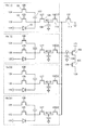
- FIG. 8 illustrates a configuration of a shared pixel circuit in which a reset circuit (transistor 111) and a source follower circuit (transistor 105) are shared by four pixels in the vertical direction.
- the pixel 10a '(pixels 10a' [1] to [4]) includes a capacitor 109 and a transistor 110 in addition to the elements of the pixel 10a.
- One electrode of the capacitor 109 is electrically connected to the other of the source and the drain of the transistor 104.
- the other of the source and the drain of the transistor 104 is electrically connected to one of the source and the drain of the transistor 110.
- the other of the source and the drain of the transistor 110 is electrically connected to one of the source and the drain of the transistor 111.
- One of a source and a drain of the transistor 111 is electrically connected to a gate of the transistor 105.
- the other electrode of the capacitor 109 and the other of the source and the drain of the transistor 111 are electrically connected to a reference potential line such as a GND wiring.
- the gate of the transistor 110 is electrically connected to the wiring 130.
- the gate of the transistor 111 is electrically connected to the wiring 131.
- the wiring 130 (the wirings 130 [1] to [4]) and the wiring 131 can function as signal lines for controlling conduction of each transistor.
- a wiring to which the other of the source and the drain of the transistor 110, the one of the source and the drain of the transistor 111, and the gate of the transistor 105 in each of the pixels 10a '[1] to [4] is a node FD.
- a wiring connecting the other of the source and the drain of the transistor 104, one electrode of the capacitor 109, and one of the source and the drain of the transistor 110 is referred to as a node AD.
- the node AD has a function of holding data captured by each pixel.
- the reset potential can be, for example, GND or 0V.
- the pixel 10b and the pixel 10c can have a shared pixel circuit configuration.
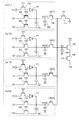
- FIG. 10 shows a configuration in which the pixel 10b is applied to a shared pixel circuit of four pixels in the vertical direction (pixels 10b '[1] to [4]).
- FIG. 11 shows a configuration in which the pixel 10c is applied to a shared pixel circuit having four pixels in the vertical direction (pixels 10c '[1] to [4]). Any of the shared pixel circuits can be operated according to the timing chart shown in FIG.
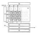
- FIG. 13 is an example of a block diagram illustrating a circuit configuration of an imaging device of one embodiment of the present invention.
- the imaging apparatus includes a pixel array 21 having pixels 10 arranged in a matrix, a circuit 22 (row driver) having a function of selecting a row of the pixel array 21, and a circuit 23 having a function of reading data from the pixels 10. And a circuit 28 for supplying a power supply potential.
- a circuit 28 for supplying a power supply potential.
- any one of the pixels 10a, 10b, 10c and its modifications can be used.
- the circuit 23 includes a circuit 24 (column driver) having a function of selecting a column of the pixel array 21, a circuit 25 (CDS circuit) for performing correlated double sampling processing on output data of the pixel 10, and a circuit 25.
- Circuit 26 (such as an A / D conversion circuit) having a function of converting analog data output from the A / D converter into digital data.
- the circuit 23 is electrically connected to the wiring 129, and can convert data output from the pixel 10 into digital data and then output the digital data to the outside.
- the output destination may be a neural network, a storage device, a display device, a communication device, or the like.
- the parameters used in the simulation are as follows.
- the voltage applied to the gate of the transistor was +26 V or +46 V as “H”, and 0 V as “L”. Note that SPICE was used as the circuit simulation software.
- FIG. 14A shows a simulation result when the pixel 10a is operated according to the timing chart of FIG. 5A.
- the horizontal axis indicates time
- the vertical axis (left) indicates the voltage supplied to the gate wirings (GL1, GL2)
- the vertical axis (right) indicates the voltage of the node FD. Note that GL1 corresponds to the wiring 125 and GL2 corresponds to the wiring 126.
- V RS1 was written to the node FD
- V RS2 was added according to the capacitance ratio, and it was confirmed that a high voltage (V RS1 + V RS2 ′) could be generated.
- FIG. 14B shows a simulation result when the pixel 10b is operated according to the timing chart of FIG. 5B. Similar to the pixel 10a, after VRS1 was written to the node FD, VRS2 was added according to the capacitance ratio, and it was confirmed that a high voltage ( VRS1 + VRS2 ') could be generated.
- a high voltage can be generated in a pixel without using a high-voltage power supply circuit, and an avalanche photodiode can operate.
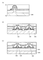
- FIGS. 15A and 15B illustrate a structure of a pixel included in an imaging device.
- the pixel illustrated in FIG. 15A is an example in which a layered structure of a layer 561 and a layer 562 is provided.
- the layer 561 includes the photoelectric conversion device 101.
- the photoelectric conversion device 101 can be a stack of a layer 565a, a layer 565b, and a layer 565c as illustrated in FIG.
- the photoelectric conversion device 101 illustrated in FIG. 15C is a pn junction photodiode.
- a p + -type semiconductor can be used for the layer 565a
- an n-type semiconductor can be used for the layer 565b
- an n + -type semiconductor can be used for the layer 565c.
- an n + -type semiconductor may be used for the layer 565a, a p-type semiconductor for the layer 565b, and a p + -type semiconductor for the layer 565c.
- a pin junction photodiode in which the layer 565b is an i-type semiconductor may be used.
- the pn junction photodiode or the pin junction photodiode can be formed using single crystal silicon. Further, the pin junction photodiode can be formed using a thin film of amorphous silicon, microcrystalline silicon, polycrystalline silicon, or the like.
- the photoelectric conversion device 101 included in the layer 561 may have a stack of a layer 566a, a layer 566b, a layer 566c, and a layer 566d as illustrated in FIG.
- the photoelectric conversion device 101 illustrated in FIG. 15D is an example of an avalanche photodiode.
- the layers 566a and 566d correspond to electrodes, and the layers 566b and 566c correspond to photoelectric conversion portions.
- a low-resistance metal layer or the like be used for the layer 566a.
- a low-resistance metal layer or the like aluminum, titanium, tungsten, tantalum, silver, or a stacked layer thereof can be used.
- a conductive layer having high light-transmitting property with respect to visible light is preferably used.
- indium oxide, tin oxide, zinc oxide, indium-tin oxide, gallium-zinc oxide, indium-gallium-zinc oxide, graphene, or the like can be used. Note that a structure in which the layer 566d is omitted can be employed.
- the layers 566b and 566c of the photoelectric conversion portion can have a configuration of a pn junction photodiode using a selenium-based material as a photoelectric conversion layer, for example. It is preferable that a selenium-based material which is a p-type semiconductor be used for the layer 566b and gallium oxide or the like which is an n-type semiconductor be used for the layer 566c.
- a photoelectric conversion device using a selenium-based material has high external quantum efficiency for visible light.
- the amplification of electrons with respect to the amount of incident light (Light) can be increased by using avalanche multiplication.
- the selenium-based material has a high light absorption coefficient, it has an advantage in production such that a photoelectric conversion layer can be formed using a thin film.
- the thin film of a selenium-based material can be formed by a vacuum evaporation method, a sputtering method, or the like.
- selenium-based material examples include crystalline selenium such as single-crystal selenium and polycrystalline selenium, amorphous selenium, copper, indium, and a compound of selenium (CIS) or a compound of copper, indium, gallium, and selenium (CIGS). Can be used.
- crystalline selenium such as single-crystal selenium and polycrystalline selenium, amorphous selenium, copper, indium, and a compound of selenium (CIS) or a compound of copper, indium, gallium, and selenium (CIGS).
- the n-type semiconductor is preferably formed using a material having a wide band gap and a property of transmitting visible light.
- a material having a wide band gap and a property of transmitting visible light For example, zinc oxide, gallium oxide, indium oxide, tin oxide, or an oxide in which they are mixed can be used.
- these materials also have a function as a hole injection blocking layer, and can reduce dark current.
- the photoelectric conversion device 101 included in the layer 561 may have a stack of a layer 567a, a layer 567b, a layer 567c, a layer 567d, and a layer 567e as illustrated in FIG.
- the photoelectric conversion device 101 illustrated in FIG. 15E is an example of an organic photoconductive film, in which the layers 567a and 567e correspond to electrodes, and the layers 567b, 567c, and 567d correspond to photoelectric conversion portions.
- One of the layers 567b and 567d of the photoelectric conversion portion can be a hole transport layer, and the other can be an electron transport layer. Further, the layer 567c can be a photoelectric conversion layer.
- the hole transport layer for example, molybdenum oxide or the like can be used.
- the electron transporting layer for example, fullerenes such as C60 and C70 or derivatives thereof can be used.
- a mixed layer (bulk heterojunction structure) of an n-type organic semiconductor and a p-type organic semiconductor can be used.
- a silicon substrate can be used as the layer 562 illustrated in FIG. 15A.
- the silicon substrate has a Si transistor and the like.
- a circuit for driving the pixel circuit, a circuit for reading an image signal, an image processing circuit, and the like can be provided in addition to the pixel circuit.
- some or all of the transistors included in the pixel circuit and the peripheral circuit (the pixel 10, the circuits 22, 23, and 28) described in Embodiment 1 can be provided in the layer 562.
- the pixel may have a stacked structure of a layer 561, a layer 563, and a layer 562 as illustrated in FIG.
- the layer 563 can include an OS transistor (eg, the transistors 102, 103, and 104 of the pixel 10a).
- the layer 562 may include a Si transistor (eg, the transistors 105 and 106 of the pixel 10a). Further, some of the transistors included in the peripheral circuit described in Embodiment 1 may be provided in the layer 563.
- the element and the peripheral circuit included in the pixel circuit can be dispersed in a plurality of layers and the element or the element and the peripheral circuit can be provided in an overlapping manner; thus, the area of the imaging device can be reduced. be able to.
- the layer 562 may be used as a supporting substrate, and the layer 561 and the layer 563 may be provided with the pixel 10 and a peripheral circuit.
- a metal oxide having an energy gap of 2 eV or more, preferably 2.5 eV or more, more preferably 3 eV or more can be used.
- a typical example is an oxide semiconductor containing indium; for example, a CAAC-OS (C-Axis Aligned Crystalline Oxide Semiconductor) or a CAC (Cloud-Aligned Composite) -OS described later can be used.
- the CAAC-OS has stable atoms in its crystal and is suitable for a transistor or the like in which reliability is emphasized.
- the CAC-OS has high mobility characteristics, and thus is suitable for a transistor that drives at high speed or the like.
- the OS transistor has an extremely low off-current characteristic of several yA / ⁇ m (current value per 1 ⁇ m of channel width) because the energy gap of the semiconductor layer is large. Further, the OS transistor has characteristics different from those of the Si transistor, such as not generating impact ionization, avalanche breakdown, and a short-channel effect, and thus can form a highly reliable circuit with high withstand voltage. In addition, variation in electrical characteristics due to non-uniformity of crystallinity, which is a problem in the Si transistor, hardly occurs in the OS transistor.
- the semiconductor layer included in the OS transistor includes an In-M-Zn-based oxide including, for example, indium, zinc, and M (a metal such as aluminum, titanium, gallium, germanium, yttrium, zirconium, lanthanum, cerium, tin, neodymium, or hafnium). Can be obtained.
- M a metal such as aluminum, titanium, gallium, germanium, yttrium, zirconium, lanthanum, cerium, tin, neodymium, or hafnium.
- the oxide semiconductor included in the semiconductor layer is an In-M-Zn-based oxide
- the atomic ratio of metal elements of a sputtering target used for forming the In-M-Zn oxide is In ⁇ M
- Zn It is preferable to satisfy ⁇ M.
- each of the atomic ratios of the semiconductor layers to be formed includes a variation of ⁇ 40% of the atomic ratio of the metal element contained in the sputtering target.
- an oxide semiconductor with a low carrier density is used as the semiconductor layer.
- the semiconductor layer has a carrier density of 1 ⁇ 10 17 / cm 3 or less, preferably 1 ⁇ 10 15 / cm 3 or less, further preferably 1 ⁇ 10 13 / cm 3 or less, more preferably 1 ⁇ 10 11 / cm 3. 3 or less, more preferably less than 1 ⁇ 10 10 / cm 3 , and an oxide semiconductor with a carrier density of 1 ⁇ 10 ⁇ 9 / cm 3 or more can be used.
- Such an oxide semiconductor is referred to as a high-purity intrinsic or substantially high-purity intrinsic oxide semiconductor. It can be said that the oxide semiconductor has a low density of defect states and has stable characteristics.
- the present invention is not limited thereto, and a transistor having an appropriate composition may be used in accordance with required semiconductor characteristics and electric characteristics (eg, field-effect mobility and threshold voltage) of the transistor.
- the carrier density and the impurity concentration of the semiconductor layer, the defect density, the atomic ratio between a metal element and oxygen, the interatomic distance, and the density be appropriate.
- the concentration of silicon or carbon (concentration obtained by secondary ion mass spectrometry) in the semiconductor layer is set to 2 ⁇ 10 18 atoms / cm 3 or less, preferably 2 ⁇ 10 17 atoms / cm 3 or less.
- an alkali metal and an alkaline earth metal may generate carriers when combined with an oxide semiconductor, which may increase off-state current of a transistor. Therefore, the concentration of alkali metal or alkaline earth metal in the semiconductor layer (concentration obtained by secondary ion mass spectrometry) is 1 ⁇ 10 18 atoms / cm 3 or less, preferably 2 ⁇ 10 16 atoms / cm 3 or less.
- the nitrogen concentration (concentration obtained by secondary ion mass spectrometry) in the semiconductor layer is preferably 5 ⁇ 10 18 atoms / cm 3 or less.
- the transistor when hydrogen is contained in the oxide semiconductor included in the semiconductor layer, oxygen reacts with oxygen bonded to a metal atom to become water, which may cause oxygen vacancies in the oxide semiconductor.
- oxygen vacancy When an oxygen vacancy is contained in a channel formation region in an oxide semiconductor, the transistor might have normally-on characteristics. Further, a defect in which hydrogen is contained in an oxygen vacancy functions as a donor, and an electron serving as a carrier may be generated. Further, in some cases, part of hydrogen is bonded to oxygen which is bonded to a metal atom to generate electrons serving as carriers. Therefore, a transistor including an oxide semiconductor containing a large amount of hydrogen is likely to have normally-on characteristics.
- a defect in which hydrogen is contained in oxygen vacancies can function as a donor of an oxide semiconductor.
- the hydrogen concentration obtained by secondary ion mass spectrometry is lower than 1 ⁇ 10 20 atoms / cm 3 , preferably 1 ⁇ 10 19 atoms / cm 3. It is less than 3 , more preferably less than 5 ⁇ 10 18 atoms / cm 3 , further preferably less than 1 ⁇ 10 18 atoms / cm 3 .
- an oxide semiconductor in which impurities such as hydrogen are sufficiently reduced is used for a channel formation region of a transistor, stable electric characteristics can be provided.
- the semiconductor layer may have a non-single-crystal structure, for example.
- the non-single-crystal structure includes, for example, a CAAC-OS (C-Axis Aligned Crystalline Oxide Semiconductor) having a crystal oriented in the c-axis, a polycrystalline structure, a microcrystalline structure, or an amorphous structure.
- CAAC-OS C-Axis Aligned Crystalline Oxide Semiconductor
- the amorphous structure has the highest density of defect states
- the CAAC-OS has the lowest density of defect states.
- An oxide semiconductor film having an amorphous structure has, for example, a disordered atomic arrangement and no crystalline component.
- an oxide semiconductor film having an amorphous structure has, for example, a completely amorphous structure and no crystal part.
- the semiconductor layer is a mixed film including two or more of an amorphous structure region, a microcrystalline structure region, a polycrystalline structure region, a CAAC-OS region, and a single crystal structure region.
- the mixed film may have a single-layer structure or a stacked structure including any two or more of the above-described regions.
- a structure of a cloud-aligned composite (CAC) -OS which is one embodiment of a non-single-crystal semiconductor layer, is described below.
- the CAC-OS is one structure of a material in which an element included in an oxide semiconductor is unevenly distributed in a size of, for example, 0.5 nm or more and 10 nm or less, preferably 1 nm or more and 2 nm or less.
- one or more metal elements are unevenly distributed in an oxide semiconductor, and a region including the metal element has a size of 0.5 nm to 10 nm, preferably 1 nm to 2 nm, or a size in the vicinity thereof.
- the state mixed by is also referred to as a mosaic shape or a patch shape.
- the oxide semiconductor preferably contains at least indium. In particular, it preferably contains indium and zinc. Also, in addition to them, aluminum, gallium, yttrium, copper, vanadium, beryllium, boron, silicon, titanium, iron, nickel, germanium, zirconium, molybdenum, lanthanum, cerium, neodymium, hafnium, tantalum, tungsten, or magnesium, etc. Or a plurality of types selected from the group consisting of:
- CAC-OS in an In-Ga-Zn oxide is an indium oxide (hereinafter referred to as InO).
- InO indium oxide
- X1 X1 is greater real than 0
- X2 Zn Y2 O Z2 X2, Y2, and Z2 is larger real than 0
- gallium An oxide hereinafter, referred to as GaO X3 (X3 is a real number larger than 0)
- Ga X4 Zn Y4 O Z4 X4, Y4, and Z4 are real numbers larger than 0)
- the material becomes mosaic by separate into, mosaic InO X1 or in X2 Zn Y2 O Z2, is a configuration in which uniformly distributed in the film (hereinafter Also referred to as a cloud-like
- the CAC-OS is a composite oxide semiconductor having a structure in which a region containing GaO X3 as a main component and a region containing In X2 Zn Y2 O Z2 or InO X1 as a main component are mixed.
- the atomic ratio of In to the element M in the first region is larger than the atomic ratio of In to the element M in the second region.
- the In concentration is higher than that of the region No. 2.
- IGZO is a common name and may refer to one compound of In, Ga, Zn, and O. Representative examples are represented by InGaO 3 (ZnO) m1 (m1 is a natural number), or In (1 + x0) Ga ( 1-x0) O 3 (ZnO) m0 (-1 ⁇ x0 ⁇ 1, m0 is an arbitrary number) Crystalline compounds may be mentioned.
- the above crystalline compound has a single crystal structure, a polycrystal structure, or a CAAC structure.
- the CAAC structure is a crystal structure in which a plurality of IGZO nanocrystals have a c-axis orientation and are connected without being oriented in the ab plane.
- CAC-OS relates to the material configuration of an oxide semiconductor.
- a CAC-OS is a material composition containing In, Ga, Zn, and O, a region which is observed as a nanoparticle mainly containing Ga as a part and a nanoparticle mainly containing In as a part.
- a region observed in a shape means a configuration in which each region is randomly dispersed in a mosaic shape. Therefore, in the CAC-OS, the crystal structure is a secondary element.
- the CAC-OS does not include a stacked structure of two or more kinds of films having different compositions.
- a structure including two layers of a film mainly containing In and a film mainly containing Ga is not included.
- the CAC-OS has a region which is observed in the form of a nanoparticle mainly including the metal element and a nanoparticle mainly including In as a part.
- the region observed in the form of particles refers to a configuration in which each of the regions is randomly dispersed in a mosaic shape.
- the CAC-OS can be formed by a sputtering method, for example, without intentionally heating the substrate.
- a sputtering method one or more selected from an inert gas (typically, argon), an oxygen gas, and a nitrogen gas are used as a deposition gas. Good. Further, it is preferable that the flow rate ratio of the oxygen gas to the total flow rate of the film formation gas at the time of film formation is as low as possible. .
- the CAC-OS is characterized in that a clear peak is not observed when measured using a ⁇ / 2 ⁇ scan by an Out-of-plane method, which is one of X-ray diffraction (XRD) measurement methods.
- XRD X-ray diffraction
- the CAC-OS includes, in an electron beam diffraction pattern obtained by irradiating an electron beam (also referred to as a nanobeam electron beam) with a probe diameter of 1 nm, a ring-shaped region (ring region) with high luminance and a ring-shaped region. Multiple bright spots are observed in the area. Therefore, the electron diffraction pattern shows that the crystal structure of the CAC-OS has an nc (nano-crystal) structure having no orientation in a planar direction and a cross-sectional direction.
- an electron beam also referred to as a nanobeam electron beam
- GaO X3 or the like is a main component by EDX mapping obtained using energy dispersive X-ray spectroscopy (EDX: Energy Dispersive X-ray spectroscopy). It can be confirmed that a certain region and a region containing In X2 Zn Y2 O Z2 or InO X1 as a main component are unevenly distributed and mixed.
- the CAC-OS has a different structure from an IGZO compound in which metal elements are uniformly distributed, and has different properties from the IGZO compound.
- the CAC-OS is phase-separated into a region containing GaO X3 or the like as a main component and a region containing In X2 Zn Y2 O Z2 or InO X1 as a main component.
- the region in which In X2 Zn Y2 O Z2 or InO X1 is a main component is a region having higher conductivity than the region in which GaO X3 or the like is a main component. That is, the conductivity of the oxide semiconductor is exhibited by the flow of carriers in a region containing In X2 Zn Y2 O Z2 or InO X1 as a main component. Therefore, high field-effect mobility ( ⁇ ) can be realized by distributing a region containing In X2 Zn Y2 O Z2 or InO X1 as a main component in a cloud shape in the oxide semiconductor.
- a region containing GaO X3 or the like as a main component is a region having higher insulating properties as compared with a region containing In X2 Zn Y2 O Z2 or InO X1 as a main component. That is, a region in which GaO X3 or the like is a main component is distributed in the oxide semiconductor, whereby a leakage current can be suppressed and a favorable switching operation can be realized.
- the insulating property caused by GaO X3 or the like and the conductivity caused by In X2 Zn Y2 O Z2 or InO X1 act complementarily to each other, so that high performance is obtained.
- On-state current (I on ) and high field-effect mobility ( ⁇ ) can be realized.
- CAC-OS is suitable as a constituent material of various semiconductor devices.
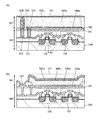
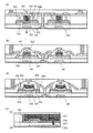
- FIG. 16A illustrates an example of a cross section of the pixel illustrated in FIG.
- the layer 561 includes, as the photoelectric conversion device 101, a pn junction photodiode including silicon as a photoelectric conversion layer.
- the layer 562 includes a Si transistor.
- FIG. 16A illustrates the transistors 102 and 104 included in a pixel circuit with the pixel 10b as an example.
- the layer 565a can be a p + -type region
- the layer 565b can be an n-type region
- the layer 565c can be an n + -type region.
- a region 536 for connecting a power supply line and the layer 565c is provided in the layer 565b.
- region 536 can be ap + type region.
- the Si transistor illustrated in FIG. 16A is a fin type having a channel formation region in a silicon substrate 540, and a cross section in the channel width direction is illustrated in FIG.
- the Si transistor may be of a planar type as shown in FIG.
- a transistor including a silicon thin film semiconductor layer 545 may be used.
- the semiconductor layer 545 can be, for example, single crystal silicon (SOI (Silicon On Insulator)) formed over the insulating layer 546 over the silicon substrate 540.
- SOI Silicon On Insulator
- FIG. 16A illustrates an example of a structure in which an element included in the layer 561 and an element included in the layer 562 are electrically connected to each other by a bonding technique.
- the insulating layer 542, the conductive layer 533, and the conductive layer 534 are provided for the layer 561.
- Each of the conductive layers 533 and 534 has a region embedded in the insulating layer 542.
- the conductive layer 533 is electrically connected to the layer 565a.
- the conductive layer 534 is electrically connected to the region 536.
- the surfaces of the insulating layer 542, the conductive layer 533, and the conductive layer 534 are flattened so that their heights are the same.
- the insulating layer 541, the conductive layer 531, and the conductive layer 532 are provided for the layer 562.
- Each of the conductive layer 531 and the conductive layer 532 has a region embedded in the insulating layer 541.
- the conductive layer 532 is electrically connected to a power supply line.
- the conductive layer 531 is electrically connected to a source or a drain of the transistor 104.
- the surfaces of the insulating layer 541, the conductive layer 531 and the conductive layer 532 are flattened so that their heights are the same.
- the main components of the conductive layer 531 and the conductive layer 533 be the same metal element. It is preferable that the main components of the conductive layer 532 and the conductive layer 534 be the same metal element. Further, the insulating layer 541 and the insulating layer 542 are preferably formed using the same components.
- the conductive layers 531, 532, 533, and 534 Cu, Al, Sn, Zn, W, Ag, Pt, Au, or the like can be used. Cu, Al, W, or Au is preferably used from the viewpoint of easy joining.
- silicon oxide, silicon oxynitride, silicon nitride oxide, silicon nitride, titanium nitride, or the like can be used.
- a surface activated bonding method in which the oxide film on the surface and the adsorption layer of impurities are removed by a sputtering process or the like, and the cleaned and activated surfaces are brought into contact with each other and bonded to each other can be used.
- a diffusion bonding method in which surfaces are bonded to each other by using both temperature and pressure can be used. In both cases, bonding at the atomic level occurs, so that a bonding excellent not only electrically but also mechanically can be obtained.
- the surfaces that have been subjected to hydrophilic treatment with oxygen plasma or the like are brought into contact with each other, and temporarily bonded, and then subjected to dehydration by heat treatment to perform the final bonding.
- a joining method or the like can be used. Since bonding at the atomic level also occurs in the hydrophilic bonding method, mechanically excellent bonding can be obtained.
- an insulating layer and a metal layer are mixed on each bonding surface. Therefore, for example, a surface activated bonding method and a hydrophilic bonding method may be combined.
- a method of cleaning the surface after polishing, performing an antioxidation treatment on the surface of the metal layer, performing a hydrophilic treatment, and then joining the metal layer can be used.
- the surface of the metal layer may be made of a non-oxidizable metal such as Au, and may be subjected to a hydrophilic treatment. Note that a joining method other than the method described above may be used.
- FIG. 16B is a cross-sectional view in the case where a pn junction photodiode including a selenium-based material as a photoelectric conversion layer is used for the pixel layer 561 illustrated in FIG. It has a layer 566a as one electrode, layers 566b and 566c as a photoelectric conversion layer, and a layer 566d as the other electrode.
- the layer 561 can be formed directly on the layer 562.
- the layer 566a is electrically connected to a source or a drain of the transistor 104.
- the layer 566d is electrically connected to a power supply line through a conductive layer 537. Note that when an organic photoconductive film is used for the layer 561, the connection with the transistor is similar.
- FIG. 18A illustrates an example of a cross section of the pixel illustrated in FIG.
- the layer 561 includes, as the photoelectric conversion device 101, a pn junction photodiode including silicon as a photoelectric conversion layer.
- the layer 562 includes a Si transistor, and FIG. 18A illustrates the transistors 105 and 106 included in a pixel circuit, using the pixel 10b as an example.
- the layer 563 includes an OS transistor and illustrates the transistors 102 and 104 included in a pixel circuit. The structure example in which the layer 561 and the layer 563 obtain electrical connection by bonding is illustrated.
- FIG. 19A illustrates details of the OS transistor.
- an insulating layer is provided over a stack of an oxide semiconductor layer and a conductive layer, and a groove which reaches the oxide semiconductor layer is provided, whereby a source electrode 205 and a drain electrode 206 are formed. This is an alignment type configuration.
- the OS transistor can have a structure including a gate electrode 201 and a gate insulating film 202 in addition to a channel formation region, a source region 203, and a drain region 204 formed in the oxide semiconductor layer. At least the gate insulating film 202 and the gate electrode 201 are provided in the groove. An oxide semiconductor layer 207 may be further provided in the groove.
- the OS transistor may have a self-aligned structure in which a source region and a drain region are formed in an oxide semiconductor layer using the gate electrode 201 as a mask.
- a non-self-aligned top-gate transistor including a region where the source electrode 205 or the drain electrode 206 and the gate electrode 201 overlap with each other may be used.
- the transistors 102 and 104 have a structure including the back gate 535, a structure without a back gate may be employed.
- the back gate 535 may be electrically connected to a front gate of a transistor provided to be opposed to the transistor as illustrated in a cross-sectional view in the channel width direction of the transistor illustrated in FIG. Note that FIG. 19D illustrates the transistor in FIG. 18A as an example, but the same applies to transistors having other structures. Further, a configuration in which a fixed potential different from that of the front gate may be supplied to the back gate 535 may be employed.
- An insulating layer 543 having a function of preventing diffusion of hydrogen is provided between a region where the OS transistor is formed and a region where the Si transistor is formed. Hydrogen in the insulating layer provided near the channel formation region of the transistors 105 and 106 terminates dangling bonds of silicon. On the other hand, hydrogen in the insulating layer provided in the vicinity of the channel formation regions of the transistors 102 and 104 is one of the factors that generate carriers in the oxide semiconductor layer.
- the insulating layer 543 for example, aluminum oxide, aluminum oxynitride, gallium oxide, gallium oxynitride, yttrium oxide, yttrium oxynitride, hafnium oxide, hafnium oxynitride, yttria-stabilized zirconia (YSZ), or the like can be used.
- aluminum oxide, aluminum oxynitride, gallium oxide, gallium oxynitride, yttrium oxide, yttrium oxynitride, hafnium oxide, hafnium oxynitride, yttria-stabilized zirconia (YSZ), or the like can be used.
- FIG. 18B is a cross-sectional view in the case where a pn junction photodiode including a selenium-based material as a photoelectric conversion layer is used for the pixel layer 561 illustrated in FIG.
- the layer 561 can be formed directly on the layer 563.
- the layers 561, 562, and 563 the above description can be referred to. Note that when an organic photoconductive film is used for the layer 561, the connection with the transistor is similar.
- FIG. 20A is a perspective view illustrating an example in which a color filter and the like are added to pixels of the imaging device of one embodiment of the present invention. In the perspective view, cross sections of a plurality of pixels are also shown.
- An insulating layer 580 is formed over the layer 561 where the photoelectric conversion device 101 is formed.
- a silicon oxide film with high light-transmitting property with respect to visible light can be used.
- a silicon nitride film may be stacked as a passivation film.
- a dielectric film such as hafnium oxide may be laminated as an antireflection film.
- a light-blocking layer 581 may be formed over the insulating layer 580.
- the light-blocking layer 581 has a function of preventing color mixture of light passing through the upper color filter.
- a metal layer such as aluminum or tungsten can be used. Further, the metal layer and a dielectric film having a function as an antireflection film may be stacked.
- An organic resin layer 582 can be provided as a planarization film over the insulating layer 580 and the light-blocking layer 581.
- a color filter 583 (color filters 583a, 583b, 583c) is formed for each pixel. For example, by assigning colors such as R (red), G (green), B (blue), Y (yellow), C (cyan), and M (magenta) to the color filters 583a, 583b, 583c, Can be obtained.
- An insulating layer 586 having a property of transmitting visible light can be provided over the color filter 583.
- an optical conversion layer 585 may be used instead of the color filter 583.
- an infrared imaging device can be obtained.
- a far-infrared imaging device can be obtained.
- an ultraviolet imaging device can be obtained.
- an imaging device that obtains an image in which the intensity of radiation used in an X-ray imaging device or the like is visualized can be obtained.
- radiation such as X-rays transmitted through a subject enters a scintillator, it is converted into light (fluorescence) such as visible light or ultraviolet light by a photoluminescence phenomenon. Then, the photoelectric conversion device 101 detects the light to acquire image data.
- the imaging device having the above configuration may be used for a radiation detector or the like.
- the scintillator includes a substance that, when irradiated with radiation such as X-rays or gamma rays, absorbs the energy and emits visible light or ultraviolet light.
- radiation such as X-rays or gamma rays
- Gd 2 O 2 S Tb
- Gd 2 O 2 S Pr
- Gd 2 O 2 S Eu
- BaFCl Eu
- NaI, CsI, CaF 2 , BaF 2 , CeF 3 LiF, LiI, ZnO, etc.
- Those dispersed in a resin or ceramics can be used.
- a microlens array 584 may be provided over the color filter 583. Light that passes through the individual lenses of the microlens array 584 passes through the color filter 583 directly below, and irradiates the photoelectric conversion device 101. Further, a microlens array 584 may be provided over the optical conversion layer 585 illustrated in FIG.
- the structure of the imaging device can be used for the image sensor chip.
- FIG. 21A1 is an external perspective view of the upper surface side of a package containing an image sensor chip.
- the package includes a package substrate 410 for fixing the image sensor chip 450 (see FIG. 21A3), a cover glass 420, an adhesive 430 for bonding the two, and the like.
- FIG. 21A2 is an external perspective view of the lower surface side of the package.
- a BGA Bit grid array
- BGA All grid array
- LGA Land Grid Array
- PGA Peripheral Component Interconnect
- FIG. 21 (A3) is a perspective view of the package illustrated with the cover glass 420 and a part of the adhesive 430 omitted.
- An electrode pad 460 is formed on the package substrate 410, and the electrode pad 460 and the bump 440 are electrically connected through a through hole.
- the electrode pad 460 is electrically connected to the image sensor chip 450 by a wire 470.
- FIG. 21 (B1) is an external perspective view of the upper side of a camera module in which an image sensor chip is housed in a lens-integrated package.
- the camera module includes a package substrate 411 for fixing the image sensor chip 451, a lens cover 421, a lens 435, and the like.
- an IC chip 490 (see FIG. 21B3) having functions such as a driving circuit and a signal conversion circuit of the imaging device is provided between the package substrate 411 and the image sensor chip 451 (see FIG. 21B3). And has a configuration as a SiP (System @ in ⁇ package).
- FIG. 21B2 is an external perspective view of the lower surface side of the camera module.
- the lower surface and the side surface of the package substrate 411 have a QFN (Quad flat no-lead package) in which mounting lands 441 are provided. Note that this configuration is an example, and a QFP (Quad @ flat @ package) or the aforementioned BGA may be provided.
- FIG. 21 (B3) is a perspective view of the module illustrated with the lens cover 421 and a part of the lens 435 omitted.
- the land 441 is electrically connected to the electrode pad 461, and the electrode pad 461 is electrically connected to the image sensor chip 451 or the IC chip 490 by a wire 471.
- the image sensor chip By mounting the image sensor chip in the above-described package, mounting on a printed circuit board or the like becomes easy, and the image sensor chip can be incorporated into various semiconductor devices and electronic devices.
- a display device As an electronic device that can use the imaging device of one embodiment of the present invention, a display device, a personal computer, an image storage device or an image reproducing device provided with a recording medium, a mobile phone, a game machine including a mobile device, and a mobile data terminal , E-book terminal, video camera, digital still camera, goggle type display (head mounted display), navigation system, sound reproduction device (car audio, digital audio player, etc.), copier, facsimile, printer, multifunction printer , An automatic teller machine (ATM), a vending machine, and the like. Specific examples of these electronic devices are illustrated in FIGS.
- FIG. 22A illustrates an example of a mobile phone, which includes a housing 981, a display portion 982, operation buttons 983, an external connection port 984, a speaker 985, a microphone 986, a camera 987, and the like.
- the mobile phone includes a touch sensor in the display portion 982. All operations such as making a call and inputting characters can be performed by touching the display portion 982 with a finger, a stylus, or the like.
- the imaging device of one embodiment of the present invention can be applied to an element for acquiring an image in the mobile phone.
- FIG. 22B illustrates a portable data terminal, which includes a housing 911, a display portion 912, a speaker 913, a camera 919, and the like.
- Information can be input and output using the touch panel function of the display portion 912.
- a character or the like can be recognized from an image acquired by the camera 919, and the character can be output as sound using the speaker 913.
- the imaging device of one embodiment of the present invention can be applied to an element for acquiring an image in the portable data terminal.
- FIG. 22C illustrates a monitoring camera, which includes a support base 951, a camera unit 952, a protective cover 953, and the like.
- the camera unit 952 is provided with a rotation mechanism and the like, and can be installed on the ceiling to capture an image of the entire periphery.
- the imaging device of one embodiment of the present invention can be applied to an element for acquiring an image in the camera unit.
- the surveillance camera is a conventional name and does not limit the use.
- a device having a function as a surveillance camera is also called a camera or a video camera.
- FIG. 22D illustrates a video camera, which includes a first housing 971, a second housing 972, a display portion 973, operation keys 974, a lens 975, a connection portion 976, a speaker 977, a microphone 978, and the like.
- the operation keys 974 and the lens 975 are provided on the first housing 971, and the display portion 973 is provided on the second housing 972.
- the imaging device of one embodiment of the present invention can be applied to an element for acquiring an image in the video camera.
- FIG. 22E illustrates a digital camera, which includes a housing 961, a shutter button 962, a microphone 963, a light-emitting portion 967, a lens 965, and the like.
- the imaging device of one embodiment of the present invention can be applied to an element for acquiring an image in the digital camera.
- FIG. 22F illustrates a wristwatch-type information terminal, which includes a display portion 932, a housing / wristband 933, a camera 939, and the like.
- the display unit 932 includes a touch panel for operating an information terminal.
- the display portion 932 and the housing / wristband 933 have flexibility and are excellent in attachment to the body.
- the imaging device of one embodiment of the present invention can be applied to an element for acquiring an image in the information terminal.
Landscapes
- Engineering & Computer Science (AREA)
- Multimedia (AREA)
- Signal Processing (AREA)
- Transforming Light Signals Into Electric Signals (AREA)
- Solid State Image Pick-Up Elements (AREA)
- Thin Film Transistor (AREA)
Priority Applications (9)
| Application Number | Priority Date | Filing Date | Title |
|---|---|---|---|
| JP2020531831A JP7336441B2 (ja) | 2018-07-27 | 2019-07-18 | 撮像装置および電子機器 |
| CN202510125274.1A CN119946458A (zh) | 2018-07-27 | 2019-07-18 | 摄像装置及电子设备 |
| US17/258,805 US11948959B2 (en) | 2018-07-27 | 2019-07-18 | Imaging device comprising first circuit and second circuit |
| KR1020217001985A KR102882109B1 (ko) | 2018-07-27 | 2019-07-18 | 촬상 장치 및 전자 기기 |
| CN201980046607.4A CN112425152B (zh) | 2018-07-27 | 2019-07-18 | 摄像装置及电子设备 |
| JP2023133796A JP7524430B2 (ja) | 2018-07-27 | 2023-08-21 | 撮像装置 |
| US18/610,634 US20240222411A1 (en) | 2018-07-27 | 2024-03-20 | Imaging device and electronic device |
| JP2024113895A JP7755695B2 (ja) | 2018-07-27 | 2024-07-17 | 撮像装置 |
| JP2025167106A JP2025188099A (ja) | 2018-07-27 | 2025-10-03 | 撮像装置 |
Applications Claiming Priority (2)
| Application Number | Priority Date | Filing Date | Title |
|---|---|---|---|
| JP2018141605 | 2018-07-27 | ||
| JP2018-141605 | 2018-07-27 |
Related Child Applications (2)
| Application Number | Title | Priority Date | Filing Date |
|---|---|---|---|
| US17/258,805 A-371-Of-International US11948959B2 (en) | 2018-07-27 | 2019-07-18 | Imaging device comprising first circuit and second circuit |
| US18/610,634 Continuation US20240222411A1 (en) | 2018-07-27 | 2024-03-20 | Imaging device and electronic device |
Publications (1)
| Publication Number | Publication Date |
|---|---|
| WO2020021398A1 true WO2020021398A1 (ja) | 2020-01-30 |
Family
ID=69182020
Family Applications (1)
| Application Number | Title | Priority Date | Filing Date |
|---|---|---|---|
| PCT/IB2019/056134 Ceased WO2020021398A1 (ja) | 2018-07-27 | 2019-07-18 | 撮像装置および電子機器 |
Country Status (5)
| Country | Link |
|---|---|
| US (2) | US11948959B2 (https=) |
| JP (4) | JP7336441B2 (https=) |
| KR (1) | KR102882109B1 (https=) |
| CN (2) | CN119946458A (https=) |
| WO (1) | WO2020021398A1 (https=) |
Families Citing this family (4)
| Publication number | Priority date | Publication date | Assignee | Title |
|---|---|---|---|---|
| WO2020021398A1 (ja) * | 2018-07-27 | 2020-01-30 | 株式会社半導体エネルギー研究所 | 撮像装置および電子機器 |
| KR20220142457A (ko) | 2020-02-20 | 2022-10-21 | 가부시키가이샤 한도오따이 에네루기 켄큐쇼 | 촬상 장치, 전자 기기, 및 이동체 |
| EP4446858B1 (en) * | 2023-04-13 | 2025-10-08 | Imec VZW | Charge sensor circuit, a detector array and a method for charge-based sensing |
| JP2024169345A (ja) * | 2023-05-23 | 2024-12-05 | ブリルニクス シンガポール プライベート リミテッド | 固体撮像装置、固体撮像装置の製造方法、および電子機器 |
Citations (3)
| Publication number | Priority date | Publication date | Assignee | Title |
|---|---|---|---|---|
| JP2011119711A (ja) * | 2009-11-06 | 2011-06-16 | Semiconductor Energy Lab Co Ltd | 半導体装置 |
| JP2011119674A (ja) * | 2009-10-30 | 2011-06-16 | Semiconductor Energy Lab Co Ltd | 半導体装置 |
| JP2017022706A (ja) * | 2015-07-07 | 2017-01-26 | 株式会社半導体エネルギー研究所 | 撮像装置およびその動作方法 |
Family Cites Families (12)
| Publication number | Priority date | Publication date | Assignee | Title |
|---|---|---|---|---|
| US7652704B2 (en) * | 2004-08-25 | 2010-01-26 | Aptina Imaging Corporation | Pixel for boosting pixel reset voltage |
| US8581257B2 (en) | 2010-04-07 | 2013-11-12 | Sharp Kabushiki Kaisha | Circuit board and display device |
| JP5275515B2 (ja) | 2010-04-30 | 2013-08-28 | シャープ株式会社 | 回路基板および表示装置 |
| JP2013197697A (ja) | 2012-03-16 | 2013-09-30 | Sony Corp | 固体撮像装置及び電子機器 |
| JP6495602B2 (ja) * | 2013-09-13 | 2019-04-03 | 株式会社半導体エネルギー研究所 | 発光装置 |
| JP2015056878A (ja) * | 2013-09-13 | 2015-03-23 | 株式会社東芝 | 固体撮像装置 |
| US9397637B2 (en) * | 2014-03-06 | 2016-07-19 | Semiconductor Energy Laboratory Co., Ltd. | Voltage controlled oscillator, semiconductor device, and electronic device |
| CN111968998B (zh) * | 2014-12-26 | 2024-12-13 | 松下知识产权经营株式会社 | 摄像装置 |
| US9876946B2 (en) * | 2015-08-03 | 2018-01-23 | Semiconductor Energy Laboratory Co., Ltd. | Imaging device and electronic device |
| US10896923B2 (en) * | 2015-09-18 | 2021-01-19 | Semiconductor Energy Laboratory Co., Ltd. | Method of operating an imaging device with global shutter system |
| US9967504B1 (en) * | 2017-04-06 | 2018-05-08 | Omnivision Technologies, Inc. | Imaging sensor with boosted photodiode drive |
| WO2020021398A1 (ja) * | 2018-07-27 | 2020-01-30 | 株式会社半導体エネルギー研究所 | 撮像装置および電子機器 |
-
2019
- 2019-07-18 WO PCT/IB2019/056134 patent/WO2020021398A1/ja not_active Ceased
- 2019-07-18 US US17/258,805 patent/US11948959B2/en active Active
- 2019-07-18 KR KR1020217001985A patent/KR102882109B1/ko active Active
- 2019-07-18 CN CN202510125274.1A patent/CN119946458A/zh active Pending
- 2019-07-18 CN CN201980046607.4A patent/CN112425152B/zh active Active
- 2019-07-18 JP JP2020531831A patent/JP7336441B2/ja active Active
-
2023
- 2023-08-21 JP JP2023133796A patent/JP7524430B2/ja active Active
-
2024
- 2024-03-20 US US18/610,634 patent/US20240222411A1/en active Pending
- 2024-07-17 JP JP2024113895A patent/JP7755695B2/ja active Active
-
2025
- 2025-10-03 JP JP2025167106A patent/JP2025188099A/ja active Pending
Patent Citations (3)
| Publication number | Priority date | Publication date | Assignee | Title |
|---|---|---|---|---|
| JP2011119674A (ja) * | 2009-10-30 | 2011-06-16 | Semiconductor Energy Lab Co Ltd | 半導体装置 |
| JP2011119711A (ja) * | 2009-11-06 | 2011-06-16 | Semiconductor Energy Lab Co Ltd | 半導体装置 |
| JP2017022706A (ja) * | 2015-07-07 | 2017-01-26 | 株式会社半導体エネルギー研究所 | 撮像装置およびその動作方法 |
Also Published As
| Publication number | Publication date |
|---|---|
| JPWO2020021398A1 (ja) | 2021-08-26 |
| CN112425152A (zh) | 2021-02-26 |
| KR102882109B1 (ko) | 2025-11-05 |
| JP7336441B2 (ja) | 2023-08-31 |
| CN119946458A (zh) | 2025-05-06 |
| US11948959B2 (en) | 2024-04-02 |
| US20240222411A1 (en) | 2024-07-04 |
| JP7755695B2 (ja) | 2025-10-16 |
| JP2023144118A (ja) | 2023-10-06 |
| US20210273007A1 (en) | 2021-09-02 |
| JP7524430B2 (ja) | 2024-07-29 |
| JP2024147701A (ja) | 2024-10-16 |
| KR20210040363A (ko) | 2021-04-13 |
| JP2025188099A (ja) | 2025-12-25 |
| CN112425152B (zh) | 2025-02-28 |
Similar Documents
| Publication | Publication Date | Title |
|---|---|---|
| JP7322239B2 (ja) | 撮像装置および電子機器 | |
| JP7524430B2 (ja) | 撮像装置 | |
| JP2020123975A (ja) | 撮像装置 | |
| JP7825762B2 (ja) | 撮像装置 | |
| JP2021027351A (ja) | 撮像装置および電子機器 | |
| WO2018185587A1 (ja) | 撮像装置および電子機器 | |
| KR102895651B1 (ko) | 촬상 패널, 촬상 장치 | |
| KR102837359B1 (ko) | 촬상 장치의 동작 방법 | |
| WO2021099889A1 (ja) | 撮像装置および電子機器 | |
| WO2021001719A1 (ja) | 撮像装置および電子機器 | |
| JP7480137B2 (ja) | 撮像装置および電子機器 | |
| WO2019243949A1 (ja) | 撮像装置の動作方法 | |
| WO2021130590A1 (ja) | 撮像装置、および電子機器 | |
| WO2021048676A1 (ja) | 撮像装置および電子機器 |
Legal Events
| Date | Code | Title | Description |
|---|---|---|---|
| 121 | Ep: the epo has been informed by wipo that ep was designated in this application |
Ref document number: 19842354 Country of ref document: EP Kind code of ref document: A1 |
|
| ENP | Entry into the national phase |
Ref document number: 2020531831 Country of ref document: JP Kind code of ref document: A |
|
| ENP | Entry into the national phase |
Ref document number: 20217001985 Country of ref document: KR Kind code of ref document: A |
|
| NENP | Non-entry into the national phase |
Ref country code: DE |
|
| 122 | Ep: pct application non-entry in european phase |
Ref document number: 19842354 Country of ref document: EP Kind code of ref document: A1 |
|
| WWG | Wipo information: grant in national office |
Ref document number: 201980046607.4 Country of ref document: CN |