WO2020009230A1 - プリント配線基板用貼付フィルム - Google Patents
プリント配線基板用貼付フィルム Download PDFInfo
- Publication number
- WO2020009230A1 WO2020009230A1 PCT/JP2019/026844 JP2019026844W WO2020009230A1 WO 2020009230 A1 WO2020009230 A1 WO 2020009230A1 JP 2019026844 W JP2019026844 W JP 2019026844W WO 2020009230 A1 WO2020009230 A1 WO 2020009230A1
- Authority
- WO
- WIPO (PCT)
- Prior art keywords
- resin
- layer
- film
- circuit pattern
- printed wiring
- Prior art date
- Legal status (The legal status is an assumption and is not a legal conclusion. Google has not performed a legal analysis and makes no representation as to the accuracy of the status listed.)
- Ceased
Links
Images


Classifications
-
- H—ELECTRICITY
- H05—ELECTRIC TECHNIQUES NOT OTHERWISE PROVIDED FOR
- H05K—PRINTED CIRCUITS; CASINGS OR CONSTRUCTIONAL DETAILS OF ELECTRIC APPARATUS; MANUFACTURE OF ASSEMBLAGES OF ELECTRICAL COMPONENTS
- H05K1/00—Printed circuits
- H05K1/02—Details
- H05K1/0213—Electrical arrangements not otherwise provided for
- H05K1/0216—Reduction of cross-talk, noise or electromagnetic interference
- H05K1/023—Reduction of cross-talk, noise or electromagnetic interference using auxiliary mounted passive components or auxiliary substances
-
- H—ELECTRICITY
- H05—ELECTRIC TECHNIQUES NOT OTHERWISE PROVIDED FOR
- H05K—PRINTED CIRCUITS; CASINGS OR CONSTRUCTIONAL DETAILS OF ELECTRIC APPARATUS; MANUFACTURE OF ASSEMBLAGES OF ELECTRICAL COMPONENTS
- H05K3/00—Apparatus or processes for manufacturing printed circuits
- H05K3/22—Secondary treatment of printed circuits
- H05K3/28—Applying non-metallic protective coatings
- H05K3/281—Applying non-metallic protective coatings by means of a preformed insulating foil
-
- B—PERFORMING OPERATIONS; TRANSPORTING
- B32—LAYERED PRODUCTS
- B32B—LAYERED PRODUCTS, i.e. PRODUCTS BUILT-UP OF STRATA OF FLAT OR NON-FLAT, e.g. CELLULAR OR HONEYCOMB, FORM
- B32B15/00—Layered products comprising a layer of metal
- B32B15/04—Layered products comprising a layer of metal comprising metal as the main or only constituent of a layer, which is next to another layer of the same or of a different material
- B32B15/08—Layered products comprising a layer of metal comprising metal as the main or only constituent of a layer, which is next to another layer of the same or of a different material of synthetic resin
- B32B15/082—Layered products comprising a layer of metal comprising metal as the main or only constituent of a layer, which is next to another layer of the same or of a different material of synthetic resin comprising vinyl resins; comprising acrylic resins
-
- B—PERFORMING OPERATIONS; TRANSPORTING
- B32—LAYERED PRODUCTS
- B32B—LAYERED PRODUCTS, i.e. PRODUCTS BUILT-UP OF STRATA OF FLAT OR NON-FLAT, e.g. CELLULAR OR HONEYCOMB, FORM
- B32B15/00—Layered products comprising a layer of metal
- B32B15/04—Layered products comprising a layer of metal comprising metal as the main or only constituent of a layer, which is next to another layer of the same or of a different material
- B32B15/08—Layered products comprising a layer of metal comprising metal as the main or only constituent of a layer, which is next to another layer of the same or of a different material of synthetic resin
- B32B15/085—Layered products comprising a layer of metal comprising metal as the main or only constituent of a layer, which is next to another layer of the same or of a different material of synthetic resin comprising polyolefins
-
- B—PERFORMING OPERATIONS; TRANSPORTING
- B32—LAYERED PRODUCTS
- B32B—LAYERED PRODUCTS, i.e. PRODUCTS BUILT-UP OF STRATA OF FLAT OR NON-FLAT, e.g. CELLULAR OR HONEYCOMB, FORM
- B32B15/00—Layered products comprising a layer of metal
- B32B15/04—Layered products comprising a layer of metal comprising metal as the main or only constituent of a layer, which is next to another layer of the same or of a different material
- B32B15/08—Layered products comprising a layer of metal comprising metal as the main or only constituent of a layer, which is next to another layer of the same or of a different material of synthetic resin
- B32B15/09—Layered products comprising a layer of metal comprising metal as the main or only constituent of a layer, which is next to another layer of the same or of a different material of synthetic resin comprising polyesters
-
- B—PERFORMING OPERATIONS; TRANSPORTING
- B32—LAYERED PRODUCTS
- B32B—LAYERED PRODUCTS, i.e. PRODUCTS BUILT-UP OF STRATA OF FLAT OR NON-FLAT, e.g. CELLULAR OR HONEYCOMB, FORM
- B32B15/00—Layered products comprising a layer of metal
- B32B15/04—Layered products comprising a layer of metal comprising metal as the main or only constituent of a layer, which is next to another layer of the same or of a different material
- B32B15/08—Layered products comprising a layer of metal comprising metal as the main or only constituent of a layer, which is next to another layer of the same or of a different material of synthetic resin
- B32B15/092—Layered products comprising a layer of metal comprising metal as the main or only constituent of a layer, which is next to another layer of the same or of a different material of synthetic resin comprising epoxy resins
-
- B—PERFORMING OPERATIONS; TRANSPORTING
- B32—LAYERED PRODUCTS
- B32B—LAYERED PRODUCTS, i.e. PRODUCTS BUILT-UP OF STRATA OF FLAT OR NON-FLAT, e.g. CELLULAR OR HONEYCOMB, FORM
- B32B15/00—Layered products comprising a layer of metal
- B32B15/04—Layered products comprising a layer of metal comprising metal as the main or only constituent of a layer, which is next to another layer of the same or of a different material
- B32B15/08—Layered products comprising a layer of metal comprising metal as the main or only constituent of a layer, which is next to another layer of the same or of a different material of synthetic resin
- B32B15/095—Layered products comprising a layer of metal comprising metal as the main or only constituent of a layer, which is next to another layer of the same or of a different material of synthetic resin comprising polyurethanes
-
- B—PERFORMING OPERATIONS; TRANSPORTING
- B32—LAYERED PRODUCTS
- B32B—LAYERED PRODUCTS, i.e. PRODUCTS BUILT-UP OF STRATA OF FLAT OR NON-FLAT, e.g. CELLULAR OR HONEYCOMB, FORM
- B32B15/00—Layered products comprising a layer of metal
- B32B15/04—Layered products comprising a layer of metal comprising metal as the main or only constituent of a layer, which is next to another layer of the same or of a different material
- B32B15/08—Layered products comprising a layer of metal comprising metal as the main or only constituent of a layer, which is next to another layer of the same or of a different material of synthetic resin
- B32B15/098—Layered products comprising a layer of metal comprising metal as the main or only constituent of a layer, which is next to another layer of the same or of a different material of synthetic resin comprising condensation resins of aldehydes, e.g. with phenols, ureas or melamines
-
- B—PERFORMING OPERATIONS; TRANSPORTING
- B32—LAYERED PRODUCTS
- B32B—LAYERED PRODUCTS, i.e. PRODUCTS BUILT-UP OF STRATA OF FLAT OR NON-FLAT, e.g. CELLULAR OR HONEYCOMB, FORM
- B32B15/00—Layered products comprising a layer of metal
- B32B15/20—Layered products comprising a layer of metal comprising aluminium or copper
-
- B—PERFORMING OPERATIONS; TRANSPORTING
- B32—LAYERED PRODUCTS
- B32B—LAYERED PRODUCTS, i.e. PRODUCTS BUILT-UP OF STRATA OF FLAT OR NON-FLAT, e.g. CELLULAR OR HONEYCOMB, FORM
- B32B27/00—Layered products comprising a layer of synthetic resin
-
- B—PERFORMING OPERATIONS; TRANSPORTING
- B32—LAYERED PRODUCTS
- B32B—LAYERED PRODUCTS, i.e. PRODUCTS BUILT-UP OF STRATA OF FLAT OR NON-FLAT, e.g. CELLULAR OR HONEYCOMB, FORM
- B32B27/00—Layered products comprising a layer of synthetic resin
- B32B27/18—Layered products comprising a layer of synthetic resin characterised by the use of special additives
-
- B—PERFORMING OPERATIONS; TRANSPORTING
- B32—LAYERED PRODUCTS
- B32B—LAYERED PRODUCTS, i.e. PRODUCTS BUILT-UP OF STRATA OF FLAT OR NON-FLAT, e.g. CELLULAR OR HONEYCOMB, FORM
- B32B27/00—Layered products comprising a layer of synthetic resin
- B32B27/18—Layered products comprising a layer of synthetic resin characterised by the use of special additives
- B32B27/20—Layered products comprising a layer of synthetic resin characterised by the use of special additives using fillers, pigments, thixotroping agents
-
- B—PERFORMING OPERATIONS; TRANSPORTING
- B32—LAYERED PRODUCTS
- B32B—LAYERED PRODUCTS, i.e. PRODUCTS BUILT-UP OF STRATA OF FLAT OR NON-FLAT, e.g. CELLULAR OR HONEYCOMB, FORM
- B32B27/00—Layered products comprising a layer of synthetic resin
- B32B27/18—Layered products comprising a layer of synthetic resin characterised by the use of special additives
- B32B27/22—Layered products comprising a layer of synthetic resin characterised by the use of special additives using plasticisers
-
- B—PERFORMING OPERATIONS; TRANSPORTING
- B32—LAYERED PRODUCTS
- B32B—LAYERED PRODUCTS, i.e. PRODUCTS BUILT-UP OF STRATA OF FLAT OR NON-FLAT, e.g. CELLULAR OR HONEYCOMB, FORM
- B32B27/00—Layered products comprising a layer of synthetic resin
- B32B27/28—Layered products comprising a layer of synthetic resin comprising synthetic resins not wholly covered by any one of the sub-groups B32B27/30 - B32B27/42
- B32B27/281—Layered products comprising a layer of synthetic resin comprising synthetic resins not wholly covered by any one of the sub-groups B32B27/30 - B32B27/42 comprising polyimides
-
- B—PERFORMING OPERATIONS; TRANSPORTING
- B32—LAYERED PRODUCTS
- B32B—LAYERED PRODUCTS, i.e. PRODUCTS BUILT-UP OF STRATA OF FLAT OR NON-FLAT, e.g. CELLULAR OR HONEYCOMB, FORM
- B32B27/00—Layered products comprising a layer of synthetic resin
- B32B27/30—Layered products comprising a layer of synthetic resin comprising vinyl (co)polymers; comprising acrylic (co)polymers
- B32B27/302—Layered products comprising a layer of synthetic resin comprising vinyl (co)polymers; comprising acrylic (co)polymers comprising aromatic vinyl (co)polymers, e.g. styrenic (co)polymers
-
- B—PERFORMING OPERATIONS; TRANSPORTING
- B32—LAYERED PRODUCTS
- B32B—LAYERED PRODUCTS, i.e. PRODUCTS BUILT-UP OF STRATA OF FLAT OR NON-FLAT, e.g. CELLULAR OR HONEYCOMB, FORM
- B32B27/00—Layered products comprising a layer of synthetic resin
- B32B27/30—Layered products comprising a layer of synthetic resin comprising vinyl (co)polymers; comprising acrylic (co)polymers
- B32B27/306—Layered products comprising a layer of synthetic resin comprising vinyl (co)polymers; comprising acrylic (co)polymers comprising vinyl acetate or vinyl alcohol (co)polymers
-
- B—PERFORMING OPERATIONS; TRANSPORTING
- B32—LAYERED PRODUCTS
- B32B—LAYERED PRODUCTS, i.e. PRODUCTS BUILT-UP OF STRATA OF FLAT OR NON-FLAT, e.g. CELLULAR OR HONEYCOMB, FORM
- B32B27/00—Layered products comprising a layer of synthetic resin
- B32B27/30—Layered products comprising a layer of synthetic resin comprising vinyl (co)polymers; comprising acrylic (co)polymers
- B32B27/308—Layered products comprising a layer of synthetic resin comprising vinyl (co)polymers; comprising acrylic (co)polymers comprising acrylic (co)polymers
-
- B—PERFORMING OPERATIONS; TRANSPORTING
- B32—LAYERED PRODUCTS
- B32B—LAYERED PRODUCTS, i.e. PRODUCTS BUILT-UP OF STRATA OF FLAT OR NON-FLAT, e.g. CELLULAR OR HONEYCOMB, FORM
- B32B27/00—Layered products comprising a layer of synthetic resin
- B32B27/32—Layered products comprising a layer of synthetic resin comprising polyolefins
-
- B—PERFORMING OPERATIONS; TRANSPORTING
- B32—LAYERED PRODUCTS
- B32B—LAYERED PRODUCTS, i.e. PRODUCTS BUILT-UP OF STRATA OF FLAT OR NON-FLAT, e.g. CELLULAR OR HONEYCOMB, FORM
- B32B27/00—Layered products comprising a layer of synthetic resin
- B32B27/36—Layered products comprising a layer of synthetic resin comprising polyesters
-
- B—PERFORMING OPERATIONS; TRANSPORTING
- B32—LAYERED PRODUCTS
- B32B—LAYERED PRODUCTS, i.e. PRODUCTS BUILT-UP OF STRATA OF FLAT OR NON-FLAT, e.g. CELLULAR OR HONEYCOMB, FORM
- B32B27/00—Layered products comprising a layer of synthetic resin
- B32B27/38—Layered products comprising a layer of synthetic resin comprising epoxy resins
-
- B—PERFORMING OPERATIONS; TRANSPORTING
- B32—LAYERED PRODUCTS
- B32B—LAYERED PRODUCTS, i.e. PRODUCTS BUILT-UP OF STRATA OF FLAT OR NON-FLAT, e.g. CELLULAR OR HONEYCOMB, FORM
- B32B27/00—Layered products comprising a layer of synthetic resin
- B32B27/40—Layered products comprising a layer of synthetic resin comprising polyurethanes
-
- B—PERFORMING OPERATIONS; TRANSPORTING
- B32—LAYERED PRODUCTS
- B32B—LAYERED PRODUCTS, i.e. PRODUCTS BUILT-UP OF STRATA OF FLAT OR NON-FLAT, e.g. CELLULAR OR HONEYCOMB, FORM
- B32B27/00—Layered products comprising a layer of synthetic resin
- B32B27/42—Layered products comprising a layer of synthetic resin comprising condensation resins of aldehydes, e.g. with phenols, ureas or melamines
-
- B—PERFORMING OPERATIONS; TRANSPORTING
- B32—LAYERED PRODUCTS
- B32B—LAYERED PRODUCTS, i.e. PRODUCTS BUILT-UP OF STRATA OF FLAT OR NON-FLAT, e.g. CELLULAR OR HONEYCOMB, FORM
- B32B3/00—Layered products comprising a layer with external or internal discontinuities or unevennesses, or a layer of non-planar shape; Layered products comprising a layer having particular features of form
- B32B3/26—Layered products comprising a layer with external or internal discontinuities or unevennesses, or a layer of non-planar shape; Layered products comprising a layer having particular features of form characterised by a particular shape of the outline of the cross-section of a continuous layer; characterised by a layer with cavities or internal voids ; characterised by an apertured layer
- B32B3/30—Layered products comprising a layer with external or internal discontinuities or unevennesses, or a layer of non-planar shape; Layered products comprising a layer having particular features of form characterised by a particular shape of the outline of the cross-section of a continuous layer; characterised by a layer with cavities or internal voids ; characterised by an apertured layer characterised by a layer formed with recesses or projections, e.g. hollows, grooves, protuberances, ribs
-
- C—CHEMISTRY; METALLURGY
- C09—DYES; PAINTS; POLISHES; NATURAL RESINS; ADHESIVES; COMPOSITIONS NOT OTHERWISE PROVIDED FOR; APPLICATIONS OF MATERIALS NOT OTHERWISE PROVIDED FOR
- C09J—ADHESIVES; NON-MECHANICAL ASPECTS OF ADHESIVE PROCESSES IN GENERAL; ADHESIVE PROCESSES NOT PROVIDED FOR ELSEWHERE; USE OF MATERIALS AS ADHESIVES
- C09J7/00—Adhesives in the form of films or foils
- C09J7/20—Adhesives in the form of films or foils characterised by their carriers
-
- C—CHEMISTRY; METALLURGY
- C09—DYES; PAINTS; POLISHES; NATURAL RESINS; ADHESIVES; COMPOSITIONS NOT OTHERWISE PROVIDED FOR; APPLICATIONS OF MATERIALS NOT OTHERWISE PROVIDED FOR
- C09J—ADHESIVES; NON-MECHANICAL ASPECTS OF ADHESIVE PROCESSES IN GENERAL; ADHESIVE PROCESSES NOT PROVIDED FOR ELSEWHERE; USE OF MATERIALS AS ADHESIVES
- C09J7/00—Adhesives in the form of films or foils
- C09J7/20—Adhesives in the form of films or foils characterised by their carriers
- C09J7/29—Laminated material
-
- C—CHEMISTRY; METALLURGY
- C09—DYES; PAINTS; POLISHES; NATURAL RESINS; ADHESIVES; COMPOSITIONS NOT OTHERWISE PROVIDED FOR; APPLICATIONS OF MATERIALS NOT OTHERWISE PROVIDED FOR
- C09J—ADHESIVES; NON-MECHANICAL ASPECTS OF ADHESIVE PROCESSES IN GENERAL; ADHESIVE PROCESSES NOT PROVIDED FOR ELSEWHERE; USE OF MATERIALS AS ADHESIVES
- C09J9/00—Adhesives characterised by their physical nature or the effects produced, e.g. glue sticks
- C09J9/02—Electrically-conducting adhesives
-
- H—ELECTRICITY
- H05—ELECTRIC TECHNIQUES NOT OTHERWISE PROVIDED FOR
- H05K—PRINTED CIRCUITS; CASINGS OR CONSTRUCTIONAL DETAILS OF ELECTRIC APPARATUS; MANUFACTURE OF ASSEMBLAGES OF ELECTRICAL COMPONENTS
- H05K1/00—Printed circuits
- H05K1/02—Details
- H05K1/0275—Security details, e.g. tampering prevention or detection
-
- H—ELECTRICITY
- H05—ELECTRIC TECHNIQUES NOT OTHERWISE PROVIDED FOR
- H05K—PRINTED CIRCUITS; CASINGS OR CONSTRUCTIONAL DETAILS OF ELECTRIC APPARATUS; MANUFACTURE OF ASSEMBLAGES OF ELECTRICAL COMPONENTS
- H05K9/00—Screening of apparatus or components against electric or magnetic fields
- H05K9/0073—Shielding materials
- H05K9/0081—Electromagnetic shielding materials, e.g. EMI, RFI shielding
-
- H—ELECTRICITY
- H05—ELECTRIC TECHNIQUES NOT OTHERWISE PROVIDED FOR
- H05K—PRINTED CIRCUITS; CASINGS OR CONSTRUCTIONAL DETAILS OF ELECTRIC APPARATUS; MANUFACTURE OF ASSEMBLAGES OF ELECTRICAL COMPONENTS
- H05K9/00—Screening of apparatus or components against electric or magnetic fields
- H05K9/0073—Shielding materials
- H05K9/0081—Electromagnetic shielding materials, e.g. EMI, RFI shielding
- H05K9/0088—Electromagnetic shielding materials, e.g. EMI, RFI shielding comprising a plurality of shielding layers; combining different shielding material structure
-
- B—PERFORMING OPERATIONS; TRANSPORTING
- B32—LAYERED PRODUCTS
- B32B—LAYERED PRODUCTS, i.e. PRODUCTS BUILT-UP OF STRATA OF FLAT OR NON-FLAT, e.g. CELLULAR OR HONEYCOMB, FORM
- B32B2250/00—Layers arrangement
- B32B2250/02—2 layers
-
- B—PERFORMING OPERATIONS; TRANSPORTING
- B32—LAYERED PRODUCTS
- B32B—LAYERED PRODUCTS, i.e. PRODUCTS BUILT-UP OF STRATA OF FLAT OR NON-FLAT, e.g. CELLULAR OR HONEYCOMB, FORM
- B32B2264/00—Composition or properties of particles which form a particulate layer or are present as additives
- B32B2264/02—Synthetic macromolecular particles
- B32B2264/0214—Particles made of materials belonging to B32B27/00
-
- B—PERFORMING OPERATIONS; TRANSPORTING
- B32—LAYERED PRODUCTS
- B32B—LAYERED PRODUCTS, i.e. PRODUCTS BUILT-UP OF STRATA OF FLAT OR NON-FLAT, e.g. CELLULAR OR HONEYCOMB, FORM
- B32B2264/00—Composition or properties of particles which form a particulate layer or are present as additives
- B32B2264/02—Synthetic macromolecular particles
- B32B2264/0214—Particles made of materials belonging to B32B27/00
- B32B2264/025—Acrylic resin particles, e.g. polymethyl methacrylate or ethylene-acrylate copolymers
-
- B—PERFORMING OPERATIONS; TRANSPORTING
- B32—LAYERED PRODUCTS
- B32B—LAYERED PRODUCTS, i.e. PRODUCTS BUILT-UP OF STRATA OF FLAT OR NON-FLAT, e.g. CELLULAR OR HONEYCOMB, FORM
- B32B2264/00—Composition or properties of particles which form a particulate layer or are present as additives
- B32B2264/02—Synthetic macromolecular particles
- B32B2264/0214—Particles made of materials belonging to B32B27/00
- B32B2264/0264—Polyamide particles
-
- B—PERFORMING OPERATIONS; TRANSPORTING
- B32—LAYERED PRODUCTS
- B32B—LAYERED PRODUCTS, i.e. PRODUCTS BUILT-UP OF STRATA OF FLAT OR NON-FLAT, e.g. CELLULAR OR HONEYCOMB, FORM
- B32B2264/00—Composition or properties of particles which form a particulate layer or are present as additives
- B32B2264/02—Synthetic macromolecular particles
- B32B2264/0214—Particles made of materials belonging to B32B27/00
- B32B2264/0292—Polyurethane particles
-
- B—PERFORMING OPERATIONS; TRANSPORTING
- B32—LAYERED PRODUCTS
- B32B—LAYERED PRODUCTS, i.e. PRODUCTS BUILT-UP OF STRATA OF FLAT OR NON-FLAT, e.g. CELLULAR OR HONEYCOMB, FORM
- B32B2264/00—Composition or properties of particles which form a particulate layer or are present as additives
- B32B2264/10—Inorganic particles
-
- B—PERFORMING OPERATIONS; TRANSPORTING
- B32—LAYERED PRODUCTS
- B32B—LAYERED PRODUCTS, i.e. PRODUCTS BUILT-UP OF STRATA OF FLAT OR NON-FLAT, e.g. CELLULAR OR HONEYCOMB, FORM
- B32B2264/00—Composition or properties of particles which form a particulate layer or are present as additives
- B32B2264/10—Inorganic particles
- B32B2264/101—Glass
-
- B—PERFORMING OPERATIONS; TRANSPORTING
- B32—LAYERED PRODUCTS
- B32B—LAYERED PRODUCTS, i.e. PRODUCTS BUILT-UP OF STRATA OF FLAT OR NON-FLAT, e.g. CELLULAR OR HONEYCOMB, FORM
- B32B2264/00—Composition or properties of particles which form a particulate layer or are present as additives
- B32B2264/10—Inorganic particles
- B32B2264/102—Oxide or hydroxide
-
- B—PERFORMING OPERATIONS; TRANSPORTING
- B32—LAYERED PRODUCTS
- B32B—LAYERED PRODUCTS, i.e. PRODUCTS BUILT-UP OF STRATA OF FLAT OR NON-FLAT, e.g. CELLULAR OR HONEYCOMB, FORM
- B32B2264/00—Composition or properties of particles which form a particulate layer or are present as additives
- B32B2264/10—Inorganic particles
- B32B2264/104—Oxysalt, e.g. carbonate, sulfate, phosphate or nitrate particles
-
- B—PERFORMING OPERATIONS; TRANSPORTING
- B32—LAYERED PRODUCTS
- B32B—LAYERED PRODUCTS, i.e. PRODUCTS BUILT-UP OF STRATA OF FLAT OR NON-FLAT, e.g. CELLULAR OR HONEYCOMB, FORM
- B32B2264/00—Composition or properties of particles which form a particulate layer or are present as additives
- B32B2264/10—Inorganic particles
- B32B2264/107—Ceramic
- B32B2264/108—Carbon, e.g. graphite particles
-
- B—PERFORMING OPERATIONS; TRANSPORTING
- B32—LAYERED PRODUCTS
- B32B—LAYERED PRODUCTS, i.e. PRODUCTS BUILT-UP OF STRATA OF FLAT OR NON-FLAT, e.g. CELLULAR OR HONEYCOMB, FORM
- B32B2264/00—Composition or properties of particles which form a particulate layer or are present as additives
- B32B2264/12—Mixture of at least two particles made of different materials
-
- B—PERFORMING OPERATIONS; TRANSPORTING
- B32—LAYERED PRODUCTS
- B32B—LAYERED PRODUCTS, i.e. PRODUCTS BUILT-UP OF STRATA OF FLAT OR NON-FLAT, e.g. CELLULAR OR HONEYCOMB, FORM
- B32B2270/00—Resin or rubber layer containing a blend of at least two different polymers
-
- B—PERFORMING OPERATIONS; TRANSPORTING
- B32—LAYERED PRODUCTS
- B32B—LAYERED PRODUCTS, i.e. PRODUCTS BUILT-UP OF STRATA OF FLAT OR NON-FLAT, e.g. CELLULAR OR HONEYCOMB, FORM
- B32B2307/00—Properties of the layers or laminate
- B32B2307/20—Properties of the layers or laminate having particular electrical or magnetic properties, e.g. piezoelectric
- B32B2307/212—Electromagnetic interference shielding
-
- B—PERFORMING OPERATIONS; TRANSPORTING
- B32—LAYERED PRODUCTS
- B32B—LAYERED PRODUCTS, i.e. PRODUCTS BUILT-UP OF STRATA OF FLAT OR NON-FLAT, e.g. CELLULAR OR HONEYCOMB, FORM
- B32B2307/00—Properties of the layers or laminate
- B32B2307/40—Properties of the layers or laminate having particular optical properties
- B32B2307/41—Opaque
-
- B—PERFORMING OPERATIONS; TRANSPORTING
- B32—LAYERED PRODUCTS
- B32B—LAYERED PRODUCTS, i.e. PRODUCTS BUILT-UP OF STRATA OF FLAT OR NON-FLAT, e.g. CELLULAR OR HONEYCOMB, FORM
- B32B2307/00—Properties of the layers or laminate
- B32B2307/50—Properties of the layers or laminate having particular mechanical properties
- B32B2307/538—Roughness
-
- B—PERFORMING OPERATIONS; TRANSPORTING
- B32—LAYERED PRODUCTS
- B32B—LAYERED PRODUCTS, i.e. PRODUCTS BUILT-UP OF STRATA OF FLAT OR NON-FLAT, e.g. CELLULAR OR HONEYCOMB, FORM
- B32B2307/00—Properties of the layers or laminate
- B32B2307/70—Other properties
- B32B2307/732—Dimensional properties
-
- B—PERFORMING OPERATIONS; TRANSPORTING
- B32—LAYERED PRODUCTS
- B32B—LAYERED PRODUCTS, i.e. PRODUCTS BUILT-UP OF STRATA OF FLAT OR NON-FLAT, e.g. CELLULAR OR HONEYCOMB, FORM
- B32B2457/00—Electrical equipment
- B32B2457/08—PCBs, i.e. printed circuit boards
-
- H—ELECTRICITY
- H05—ELECTRIC TECHNIQUES NOT OTHERWISE PROVIDED FOR
- H05K—PRINTED CIRCUITS; CASINGS OR CONSTRUCTIONAL DETAILS OF ELECTRIC APPARATUS; MANUFACTURE OF ASSEMBLAGES OF ELECTRICAL COMPONENTS
- H05K1/00—Printed circuits
- H05K1/02—Details
- H05K1/0274—Optical details, e.g. printed circuits comprising integral optical means
-
- H—ELECTRICITY
- H05—ELECTRIC TECHNIQUES NOT OTHERWISE PROVIDED FOR
- H05K—PRINTED CIRCUITS; CASINGS OR CONSTRUCTIONAL DETAILS OF ELECTRIC APPARATUS; MANUFACTURE OF ASSEMBLAGES OF ELECTRICAL COMPONENTS
- H05K2201/00—Indexing scheme relating to printed circuits covered by H05K1/00
- H05K2201/01—Dielectrics
- H05K2201/0104—Properties and characteristics in general
- H05K2201/0112—Absorbing light, e.g. dielectric layer with carbon filler for laser processing
-
- H—ELECTRICITY
- H05—ELECTRIC TECHNIQUES NOT OTHERWISE PROVIDED FOR
- H05K—PRINTED CIRCUITS; CASINGS OR CONSTRUCTIONAL DETAILS OF ELECTRIC APPARATUS; MANUFACTURE OF ASSEMBLAGES OF ELECTRICAL COMPONENTS
- H05K2201/00—Indexing scheme relating to printed circuits covered by H05K1/00
- H05K2201/01—Dielectrics
- H05K2201/0183—Dielectric layers
- H05K2201/0195—Dielectric or adhesive layers comprising a plurality of layers, e.g. in a multilayer structure
-
- H—ELECTRICITY
- H05—ELECTRIC TECHNIQUES NOT OTHERWISE PROVIDED FOR
- H05K—PRINTED CIRCUITS; CASINGS OR CONSTRUCTIONAL DETAILS OF ELECTRIC APPARATUS; MANUFACTURE OF ASSEMBLAGES OF ELECTRICAL COMPONENTS
- H05K2201/00—Indexing scheme relating to printed circuits covered by H05K1/00
- H05K2201/02—Fillers; Particles; Fibers; Reinforcement materials
- H05K2201/0203—Fillers and particles
- H05K2201/0206—Materials
- H05K2201/0209—Inorganic, non-metallic particles
-
- H—ELECTRICITY
- H05—ELECTRIC TECHNIQUES NOT OTHERWISE PROVIDED FOR
- H05K—PRINTED CIRCUITS; CASINGS OR CONSTRUCTIONAL DETAILS OF ELECTRIC APPARATUS; MANUFACTURE OF ASSEMBLAGES OF ELECTRICAL COMPONENTS
- H05K2201/00—Indexing scheme relating to printed circuits covered by H05K1/00
- H05K2201/02—Fillers; Particles; Fibers; Reinforcement materials
- H05K2201/0203—Fillers and particles
- H05K2201/0206—Materials
- H05K2201/0215—Metallic fillers
-
- H—ELECTRICITY
- H05—ELECTRIC TECHNIQUES NOT OTHERWISE PROVIDED FOR
- H05K—PRINTED CIRCUITS; CASINGS OR CONSTRUCTIONAL DETAILS OF ELECTRIC APPARATUS; MANUFACTURE OF ASSEMBLAGES OF ELECTRICAL COMPONENTS
- H05K2201/00—Indexing scheme relating to printed circuits covered by H05K1/00
- H05K2201/03—Conductive materials
- H05K2201/032—Materials
- H05K2201/0323—Carbon
-
- H—ELECTRICITY
- H05—ELECTRIC TECHNIQUES NOT OTHERWISE PROVIDED FOR
- H05K—PRINTED CIRCUITS; CASINGS OR CONSTRUCTIONAL DETAILS OF ELECTRIC APPARATUS; MANUFACTURE OF ASSEMBLAGES OF ELECTRICAL COMPONENTS
- H05K2201/00—Indexing scheme relating to printed circuits covered by H05K1/00
- H05K2201/03—Conductive materials
- H05K2201/0332—Structure of the conductor
- H05K2201/0335—Layered conductors or foils
- H05K2201/0355—Metal foils
-
- H—ELECTRICITY
- H05—ELECTRIC TECHNIQUES NOT OTHERWISE PROVIDED FOR
- H05K—PRINTED CIRCUITS; CASINGS OR CONSTRUCTIONAL DETAILS OF ELECTRIC APPARATUS; MANUFACTURE OF ASSEMBLAGES OF ELECTRICAL COMPONENTS
- H05K2201/00—Indexing scheme relating to printed circuits covered by H05K1/00
- H05K2201/07—Electric details
- H05K2201/0707—Shielding
- H05K2201/0715—Shielding provided by an outer layer of PCB
Definitions
- the present disclosure relates to an adhesive film for a printed wiring board and an electromagnetic wave shielding film.
- a first embodiment of the printed film for a printed wiring board according to the present disclosure includes a circuit pattern concealing layer, and an adhesive layer laminated with the circuit pattern concealing layer, and the circuit pattern concealing layer is provided on the side opposite to the adhesive layer.
- Rku on the surface is 2.5 or more and 3.0 or less.
- the circuit pattern hiding layer has a load length ratio (Rmr) of 5.3% or more when the cutting level is 20% on the surface opposite to the adhesive layer. , 8.5% or less.
- One embodiment of the electromagnetic wave shielding film may further include a shield layer between the circuit pattern hiding layer and the adhesive layer.
- the concealability of the circuit pattern can be improved.
- the circuit pattern 122 is made of a conductive material.
- a conductive material a metal foil or a conductive material obtained by printing and curing a mixture of a conductive filler and a resin composition can be used, but a copper foil is preferably used from the viewpoint of cost.
- the thickness of the adhesive layer 123 is not particularly limited, but is preferably 1 ⁇ m to 50 ⁇ m.
- the circuit pattern 122 cannot be directly viewed.
- the circuit pattern 122 is covered with a film having a total light transmittance of preferably 20% or less, more preferably 10% or less, and still more preferably 5% or less, it is almost impossible to directly recognize the circuit pattern 122. Become. However, unevenness is formed on the surface of the concealing layer 112 by the circuit pattern 122.
- the general circuit pattern 122 is formed by copper lines, and has a height of several ⁇ m to several tens ⁇ m.
- the height of the unevenness generated on the surface of the concealing layer 112 is several ⁇ m.
- the presence of the irregularities can be visually recognized on the surface that easily reflects light, and the circuit pattern 122 cannot be hidden.
- the relative load length ratio (Rmr) when the cutting level is 20% on the surface of the concealing layer 112 is preferably 5.3% or more, more preferably 5.4% or more, and further preferably 5.5%.
- the content is preferably 8.5% or less, more preferably 8.0% or less, still more preferably 7.8% or less, still more preferably 7.0% or less, and still more preferably 6.0% or less.
- Rmr By setting Rmr to such a value in addition to Rku, the concealment property can be further improved.
- volume (Vmc) preferably at 1.8 mL / m 2 or more, more preferably 2.0 mL / m 2 or more, more preferably set to 2.2 mL / m 2 or more, which is preferably a 3.0 mL / m 2 or less.
- the concealing layer 112 having a predetermined surface property can be formed by applying and drying these resins on the surface of the releasable base material provided with an uneven shape by embossing or the like.
- a film provided with a matte layer having irregularities on the surface may be used as the peelable substrate.
- the matte layer can be formed by applying a resin composition containing fine particles to the film surface, or by embossing the surface of the resin layer formed on the film surface.
- inorganic fine particles calcium carbonate fine particles, calcium silicate fine particles, clay, kaolin, talc, silica fine particles, glass fine particles, diatomaceous earth, mica powder, alumina fine particles, magnesium oxide fine particles, zinc oxide fine particles, barium sulfate fine particles, aluminum sulfate fine particles, Fine particles of calcium sulfate and fine particles of magnesium carbonate can be used.
- resin fine particles and inorganic fine particles can be used alone or in combination of two or more.
- a curing accelerator for a curing accelerator, a tackifier, an antioxidant, a pigment, a dye, a plasticizer, an ultraviolet absorber, an antifoaming agent, a leveling agent, a filler, a flame retardant, a viscosity control And at least one of an anti-blocking agent and the like.
- the thickness of the concealing layer 112 is not particularly limited and can be appropriately set as necessary. However, from the viewpoint of realizing concealing properties, easy formation, and securing flexibility, the thickness is preferably 1 ⁇ m or more. Preferably it is 4 ⁇ m or more, and preferably 20 ⁇ m or less, more preferably 10 ⁇ m or less, and still more preferably 5 ⁇ m or less.
- the adhesive layer 111 can be formed of at least one of a thermoplastic resin, a thermosetting resin, an active energy ray-curable resin, and the like.
- thermosetting resin for example, a phenol resin, an epoxy resin, a urethane resin, a melamine resin, a polyamide resin, an alkyd resin, or the like can be used as the thermosetting resin.
- the active energy ray-curable resin is not particularly limited.
- a polymerizable compound having at least two (meth) acryloyloxy groups in a molecule can be used. These resins may be used alone or in combination of two or more.
- the thermosetting resin includes, for example, a first resin component having a reactive first functional group, and a second resin component reacting with the first functional group.
- the first functional group can be, for example, an epoxy group, an amide group, a hydroxyl group, or the like.
- the second functional group may be selected according to the first functional group.
- the first functional group is an epoxy group, it can be a hydroxyl group, a carboxyl group, an epoxy group, an amino group, or the like.
- the first resin component is an epoxy resin
- the second resin component an epoxy-modified polyester resin, an epoxy-modified polyamide resin, an epoxy-modified acrylic resin, an epoxy-modified polyurethane polyurea resin, a carboxyl A group-modified polyester resin, a carboxyl group-modified polyamide resin, a carboxyl group-modified acrylic resin, a carboxyl group-modified polyurethane polyurea resin, a urethane-modified polyester resin, or the like can be used.
- a carboxyl group-modified polyester resin, a carboxyl group-modified polyamide resin, a carboxyl group-modified polyurethane polyurea resin, and a urethane-modified polyester resin are preferable.
- the first resin component is a hydroxyl group
- the second resin component an epoxy-modified polyester resin, an epoxy-modified polyamide resin, an epoxy-modified acrylic resin, an epoxy-modified polyurethane polyurea resin, a carboxyl-modified polyester resin, A carboxyl group-modified polyamide resin, a carboxyl group-modified acrylic resin, a carboxyl group-modified polyurethane polyurea resin, a urethane-modified polyester resin, or the like can be used.
- a carboxyl group-modified polyester resin, a carboxyl group-modified polyamide resin, a carboxyl group-modified polyurethane polyurea resin, and a urethane-modified polyester resin are preferable
- the thermosetting resin may contain a curing agent that promotes a thermosetting reaction.
- the curing agent can be appropriately selected according to the types of the first functional group and the second functional group.
- the first functional group is an epoxy group and the second functional group is a hydroxyl group
- an imidazole-based curing agent, a phenol-based curing agent, a cationic curing agent, or the like can be used. One of these can be used alone, or two or more can be used in combination.
- it may contain an antifoaming agent, an antioxidant, a viscosity modifier, a diluent, an antisettling agent, a leveling agent, a coupling agent, a coloring agent, a flame retardant, and the like as optional components.
- the thickness of the adhesive layer 111 is not particularly limited, but is preferably 1 ⁇ m to 50 ⁇ m from the viewpoint of securing adhesiveness and flexibility.
- the adhesive layer 111 may be a layer having tackiness in an environment at normal temperature (for example, 20 ° C.), that is, a layer having a so-called adhesive property. Since the adhesive layer 111 has tackiness in a normal temperature environment, the printed film 101 can be easily attached to an arbitrary position on the printed circuit board 102.
- a conductive filler may be added to the adhesive layer 111 to make the adhesive layer 111 a conductive adhesive layer having conductivity.
- the adhesive film 101 can be used as an electromagnetic wave shielding film.
- the conductive adhesive layer 111 may be connected to a ground pattern provided on the printed wiring board 102.
- the conductive filler is not particularly limited, but for example, a metal filler, a metal-coated resin filler, a carbon filler, and a mixture thereof can be used.
- the metal filler include copper powder, silver powder, nickel powder, silver-coated copper powder, gold-coated copper powder, silver-coated nickel powder, and gold-coated nickel powder. These metal powders can be produced by an electrolytic method, an atomizing method, a reducing method, or the like. Among them, any of silver powder, silver-coated copper powder and copper powder is preferable.
- the conductive filler has an average particle diameter of preferably 1 ⁇ m or more, more preferably 3 ⁇ m or more, preferably 50 ⁇ m or less, more preferably 40 ⁇ m or less from the viewpoint of contact between the fillers.
- the shape of the conductive filler is not particularly limited, and may be spherical, flake-like, dendritic, or fibrous.
- a shield layer 113 may be provided between the concealing layer 112 and the adhesive layer 111 as shown in FIG.
- the shield layer 113 can be formed using a metal foil, a deposited film, a conductive filler, or the like.
- the metal foil is not particularly limited, but may be a foil made of any one of nickel, copper, silver, tin, gold, palladium, aluminum, chromium, titanium, zinc, or an alloy containing two or more.
- the thickness of the metal foil is not particularly limited, but is preferably 0.5 ⁇ m or more, and more preferably 1.0 ⁇ m or more.
- the thickness of the metal foil is preferably 12 ⁇ m or less, more preferably 10 ⁇ m or less, and even more preferably 7 ⁇ m or less.
- the thickness of the metal layer is 12 ⁇ m or less, good breaking elongation can be secured.
- the deposited film is not particularly limited, but can be formed by depositing nickel, copper, silver, tin, gold, palladium, aluminum, chromium, titanium, zinc, or the like.
- an electrolytic plating method an electroless plating method, a sputtering method, an electron beam evaporation method, a vacuum evaporation method, a chemical vapor deposition (CVD) method, a metal organic deposition (MOCVD) method, or the like can be used.
- CVD chemical vapor deposition
- MOCVD metal organic deposition
- the shield layer 113 can be formed by applying a solvent containing the conductive filler to the surface of the concealing layer 112 and drying the same.
- a metal filler a metal-coated resin filler, a carbon filler, and a mixture thereof can be used.
- the metal filler copper powder, silver powder, nickel powder, silver-coated copper powder, gold-coated copper powder, silver-coated nickel powder, gold-coated nickel powder and the like can be used. These metal powders can be prepared by an electrolytic method, an atomizing method, or a reducing method. Examples of the shape of the metal powder include a spherical shape, a flake shape, a fibrous shape, and a dendritic shape.
- the thickness of the shield layer 113 may be appropriately selected according to the required electromagnetic shielding effect and the resistance to repeated bending and sliding.
- the adhesive film 101 has a total light transmittance of preferably 20% or less, more preferably 10% or less, and still more preferably 5% or less. By setting the total light transmittance to 20% or less, it is possible to make it difficult to directly recognize the circuit pattern 122 when the adhesive film 101 is attached to the printed wiring board 102.
- a coloring agent, a conductive filler, or the like may be added to the concealing layer 112 and / or the adhesive layer 111.
- the shield layer 113 made of a metal foil or the like is provided, the total light transmittance can be made substantially zero.
- the total light transmittance can be measured in accordance with JIS K7136.
- a PET film The surface of a 25 ⁇ m-thick polyethylene terephthalate film (hereinafter referred to as a PET film) was sprayed with fine particles of dry ice to form irregularities, and then a release layer made of a melamine-based resin was provided.
- a PET film polyethylene terephthalate film
- a matte layer composition comprising silica particles, a melamine-based resin, and toluene was prepared, applied to the surface of a 25 ⁇ m-thick polyethylene terephthalate film using a wire bar, dried by heating and peeled to have a 5 ⁇ m-thick matte layer.
- the base material 2 was obtained.
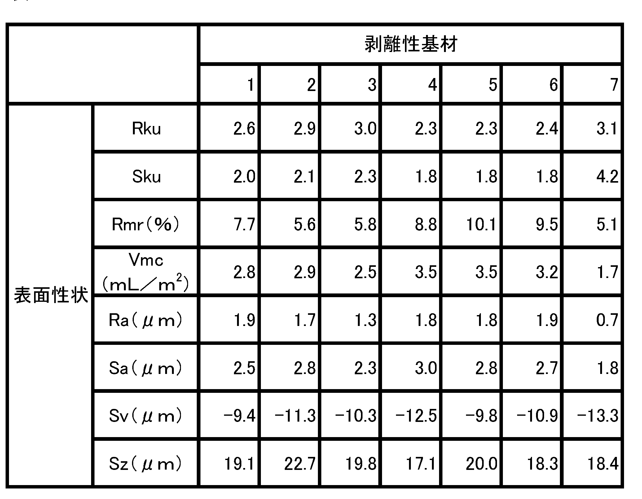
- release substrates 3 to 7 having different surface conditions were similarly obtained.
- Table 1 summarizes the surface properties of the surfaces of the peelable substrates 1 to 5 (the surfaces on which the concealing layer is formed).
- ⁇ Preparation of adhesive film> The concealing layer formed on the surface of the peelable substrate and the adhesive layer formed on the surface of the support film are bonded together, and heated at a pressure of 5 MPa using a pair of metal rolls heated to 100 ° C. Pressure was applied to obtain an adhesive film. The total light transmittance of the obtained adhesive film was 5% or less.
- Example 1 An adhesive film was formed from the concealing layer formed using the peelable substrate 1, and a substrate for evaluation was obtained.
- Rku on the surface of the concealing layer of the evaluation substrate after removing the peelable substrate was 2.6, and Sku was 2.0.
- the cutting level was 20%
- Rmr was 7.7%
- the load area ratio separating the core portion and the protruding ridge portion was 10%
- the load area ratio separating the core portion and the protruding valley portion was 80%.
- Vmc at that time was 2.8 mL / m 2 .
- Ra, Sa, Sv and Sz were 1.8 ⁇ m, 2.3 ⁇ m, ⁇ 10.2 ⁇ m and 18.3 ⁇ m, respectively. In the visual inspection, the circuit pattern could not be visually recognized, and the concealing property was very good.
- Example 2 An evaluation substrate was obtained in the same manner as in Example 1 except that the peelable substrate 2 was used.
- Rku on the surface of the concealing layer of the evaluation substrate after removing the peelable substrate was 2.9, and Sku was 2.1.
- Rmr was 5.6% and Vmc was 2.9 mL / m 2 .
- Ra, Sa, Sv and Sz were 1.8 ⁇ m, 2.5 ⁇ m, ⁇ 12.9 ⁇ m and 23.6 ⁇ m, respectively. In the visual inspection, the circuit pattern could not be visually recognized, and the concealing property was very good.
- Example 1 An evaluation substrate was obtained in the same manner as in Example 1 except that the peelable substrate 4 was used.
- the Rku on the surface of the concealing layer of the evaluation substrate after removing the peelable substrate was 2.3 and the Sku was 1.8.
- Rmr was 8.8% and Vmc was 3.5 mL / m 2 .
- Ra, Sa, Sv and Sz were 2.0 ⁇ m, 2.7 ⁇ m, ⁇ 11.5 ⁇ m and 18.8 ⁇ m, respectively. In the visual inspection, the circuit pattern was visible, and the concealing property was poor.
- Example 3 An evaluation substrate was obtained in the same manner as in Example 1 except that the peelable substrate 6 was used.
- Rku on the surface of the concealing layer of the evaluation substrate after removing the peelable substrate was 2.4, and Sku was 1.8.
- Rmr was 9.5% and Vmc was 3.2 mL / m 2 .
- Ra, Sa, Sv and Sz were 1.9 ⁇ m, 2.6 ⁇ m, ⁇ 10.0 ⁇ m and 16.9 ⁇ m, respectively. In the visual inspection, the circuit pattern was visible, and the concealing property was poor.
- Example 4 An evaluation substrate was obtained in the same manner as in Example 1 except that the peelable substrate 7 was used.
- Rku on the surface of the concealing layer of the evaluation substrate after removing the peelable substrate was 3.1, and Sku was 4.2.
- Rmr was 5.1% and Vmc was 1.7 mL / m 2 .
- Ra, Sa, Sv and Sz were 0.7 ⁇ m, 1.5 ⁇ m, ⁇ 11.1 ⁇ m and 16.2 ⁇ m, respectively. In the visual inspection, the circuit pattern was visible, and the concealing property was poor.
- Adhesive film 101
- Adhesive film 102
- Printed wiring board 111
- Concealment layer 113
- Shield layer 121
- Base layer 122
- Circuit pattern 123
- Adhesive layer 124 Insulating film
Landscapes
- Engineering & Computer Science (AREA)
- Microelectronics & Electronic Packaging (AREA)
- Organic Chemistry (AREA)
- Chemical & Material Sciences (AREA)
- Physics & Mathematics (AREA)
- Electromagnetism (AREA)
- Manufacturing & Machinery (AREA)
- Computer Security & Cryptography (AREA)
- Shielding Devices Or Components To Electric Or Magnetic Fields (AREA)
- Non-Metallic Protective Coatings For Printed Circuits (AREA)
- Structure Of Printed Boards (AREA)
- Adhesive Tapes (AREA)
- Adhesives Or Adhesive Processes (AREA)
- Laminated Bodies (AREA)
Abstract
Description
厚み25μmのポリエチレンテレフタレートフィルム(以下、PETフィルム)の表面に、ドライアイス微粒子を吹き付けて凹凸を形成させた後、メラミン系樹脂からなる剥離層を設け、剥離性基材1を得た。
固形分量が20質量%となるように、トルエンにビスフェノールA型エポキシ系樹脂(三菱化学製、jER1256)を100質量部、硬化剤として(三菱化学製、ST14)を0.1質量部、黒色系着色剤としてカーボン粒子(東海カーボン製、トーカブラック#8300/F)を15質量部配合し、隠蔽層組成物を調製した。この組成物を、剥離性基材の表面にワイヤーバーを用いて塗布し、加熱乾燥して、剥離性基材の表面に厚さ5μmの隠蔽層を作製した。
固形分量が20質量%となるように、トルエンにビスフェノールA型エポキシ系樹脂(三菱化学製、jER1256)を100質量部、硬化剤(三菱化学製、ST14)を0.1質量部添加し、撹拌混合して接着剤層組成物を調製した。得られた接着剤層組成物を、表面を離型処理したPETフィルム(以下、支持フィルム)にワイヤーバーを用いて塗布し、加熱乾燥することで、支持フィルム表面に厚さ5μmの接着剤層を形成した。
剥離性基材の表面に形成された隠蔽層と、支持フィルムの表面に形成された接着剤層とを貼り合わせ、100℃に加熱した1対の金属ロールを用いて、5MPaの圧力で加熱加圧して貼付フィルムを得た。得られた貼付フィルムの全光線透過率は、5%以下であった。
得られた貼付フィルムとプリント配線基板とを、プレス機を用いて温度:170℃、時間:3分、圧力:2~3MPaの条件で接着した後、剥離性基材をはがして評価用基板を作製した。
コンフォーカル顕微鏡(Lasertec社製、OPTELICS HYBRID、対物レンズ20倍)を用い、JISB0601:2001に準拠して、表面の任意の5か所を測定した。この後、データ解析ソフト(LMeye7)を用いて傾き補正を行い、Rku、Rmr及びRaを測定した。また、ISO25178に準拠して、表面の任意の5か所を測定した。この後、データ解析ソフト(LMeye7)を用いて表面の傾き補正を行い、Sku、Vmr、Sa、Sv及びSzを測定した。なお、Sフィルタのカットオフ波長は0.0025mm、Lフィルタのカットオフ波長は0.8mmとした。また、各数値は5か所を測定した値の平均値とした。
評価用基板を、平らなテーブル面上に置き、シールド配線基板の表面の照度が500ルクスの環境下で、評価用基板からの高さが30cmで、45度の角度において、隠蔽層側から回路パターンが視認できるかどうか評価した。回路パターンを視認できない場合を隠蔽性が良好(○)とし、回路パターンを視認できる場合を隠蔽性が不良(×)とした。
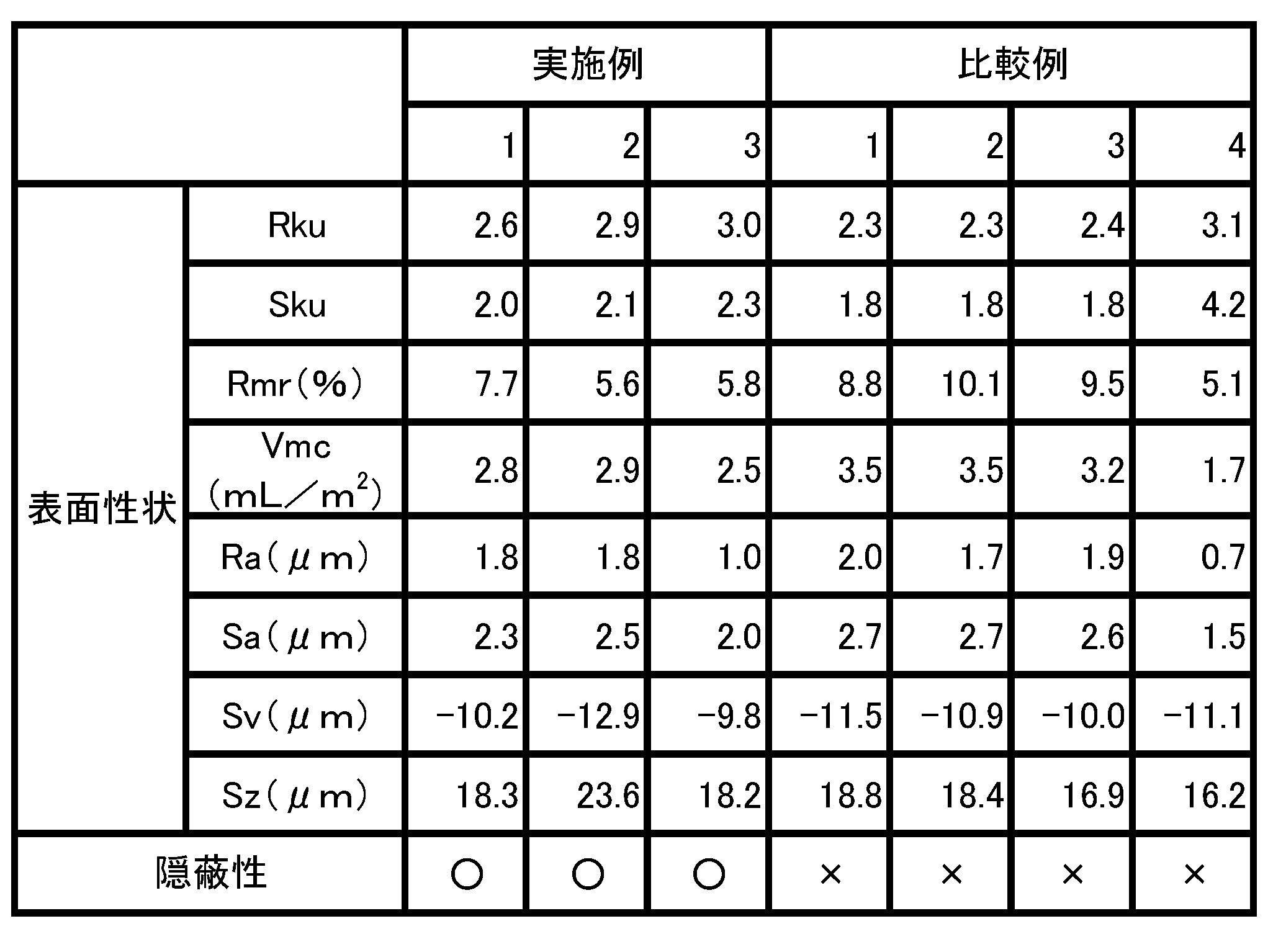
剥離性基材1を用いて形成した隠蔽層により貼付フィルムを作成し、評価用基板を得た。剥離性基材を除去した後の評価用基板の隠蔽層の表面におけるRkuは2.6、Skuは2.0であった。切断レベルが20%の場合のRmrは7.7%、コア部と突出山部とを分離する負荷面積率を10%、コア部と突出谷部とを分離する負荷面積率を80%としたときのVmcは2.8mL/m2であった。また、Ra、Sa、Sv及びSzは、それぞれ、1.8μm、2.3μm、-10.2μm及び18.3μmであった。目視による検査では、回路パターンを視認することができず、隠蔽性は非常に良好であった。
剥離性基材2を用いた他は、実施例1と同様にして評価用基板を得た。剥離性基材を除去した後の評価用基板の隠蔽層の表面におけるRkuは2.9、Skuは2.1であった。Rmrは5.6%、Vmcは2.9mL/m2であった。また、Ra、Sa、Sv及びSzは、それぞれ、1.8μm、2.5μm、-12.9μm及び23.6μmであった。目視による検査では、回路パターンを視認することができず、隠蔽性は非常に良好であった。
剥離性基材3を用いた他は、実施例1と同様にして評価用基板を得た。剥離性基材を除去した後の評価用基板の隠蔽層の表面におけるRkuは3.0、Skuは2.3であった。Rmrは5.8%、Vmcは2.5mL/m2であった。また、Ra、Sa、Sv及びSzは、それぞれ、1.0μm、2.0μm、-9.8μm及び18.2μmであった。目視による検査では、回路パターンを視認することができず、隠蔽性は非常に良好であった。
剥離性基材4を用いた他は、実施例1と同様にして評価用基板を得た。剥離性基材を除去した後の評価用基板の隠蔽層の表面におけるRkuは2.3、Skuは1.8であった。Rmrは8.8%、Vmcは3.5mL/m2であった。また、Ra、Sa、Sv及びSzは、それぞれ、2.0μm、2.7μm、-11.5μm及び18.8μmであった。目視による検査において、回路パターンを視認することができ、隠蔽性は不良であった。
剥離性基材5を用いた他は、実施例1と同様にして評価用基板を得た。剥離性基材を除去した後の評価用基板の隠蔽層の表面におけるRkuは2.3、Skuは1.8であった。Rmrは10.1%、Vmcは3.5mL/m2であった。また、Ra、Sa、Sv及びSzは、それぞれ、1.7μm、2.7μm、-10.9μm及び18.4μmであった。目視による検査において、回路パターンを視認することができ、隠蔽性は不良であった。
剥離性基材6を用いた他は、実施例1と同様にして評価用基板を得た。剥離性基材を除去した後の評価用基板の隠蔽層の表面におけるRkuは2.4、Skuは1.8であった。Rmrは9.5%、Vmcは3.2mL/m2であった。また、Ra、Sa、Sv及びSzは、それぞれ、1.9μm、2.6μm、-10.0μm及び16.9μmであった。目視による検査において、回路パターンを視認することができ、隠蔽性は不良であった。
剥離性基材7を用いた他は、実施例1と同様にして評価用基板を得た。剥離性基材を除去した後の評価用基板の隠蔽層の表面におけるRkuは3.1、Skuは4.2であった。Rmrは5.1%、Vmcは1.7mL/m2であった。また、Ra、Sa、Sv及びSzは、それぞれ、0.7μm、1.5μm、-11.1μm及び16.2μmであった。目視による検査において、回路パターンを視認することができ、隠蔽性は不良であった。
102 プリント配線基板
111 接着剤層
112 隠蔽層
113 シールド層
121 ベース層
122 回路パターン
123 接着剤層
124 絶縁フィルム
Claims (6)
- 回路パターン隠蔽層と、
前記回路パターン隠蔽層と積層された接着剤層とを備え、
前記回路パターン隠蔽層は、前記接着剤層と反対側の面におけるRkuが2.5以上、3.0以下である、プリント配線基板用貼付フィルム。 - 前記回路パターン隠蔽層は、前記接着剤層と反対側の面における、切断レベルが20%の場合のRmrが5.3%以上、8.5%以下である、請求項1に記載のプリント配線基板用貼付フィルム。
- 回路パターン隠蔽層と、
前記回路パターン隠蔽層と積層された接着剤層とを備え、
前記回路パターン隠蔽層は、前記接着剤層と反対側の面におけるSkuが1.8以上、4.0以下である、プリント配線基板用貼付フィルム。 - 前記回路パターン隠蔽層は、前記接着剤層と反対側の面における、コア部と突出山部とを分離する負荷面積率を10%、コア部と突出谷部とを分離する負荷面積率を80%としたときのVmcが2.0mL/m2以上、3.0mL/m2以下である、請求項3に記載のプリント配線基板用貼付フィルム。
- 請求項1~4のいずれか1項に記載のプリント配線基板用貼付フィルムを備え、
前記接着剤層が導電性接着剤層である、電磁波シールドフィルム。 - 前記回路パターン隠蔽層と、前記接着剤層との間に、シールド層をさらに備えている、請求項5に記載の電磁波シールドフィルム。
Priority Applications (4)
| Application Number | Priority Date | Filing Date | Title |
|---|---|---|---|
| CN201980057276.4A CN112586096B (zh) | 2018-07-06 | 2019-07-05 | 印制线路基材用贴附膜 |
| US17/256,931 US11937365B2 (en) | 2018-07-06 | 2019-07-05 | Affixation film for printed wiring board |
| JP2020509529A JP6722370B2 (ja) | 2018-07-06 | 2019-07-05 | プリント配線基板用貼付フィルム |
| KR1020217003746A KR102479873B1 (ko) | 2018-07-06 | 2019-07-05 | 프린트 배선 기판용 접착 필름 |
Applications Claiming Priority (2)
| Application Number | Priority Date | Filing Date | Title |
|---|---|---|---|
| JP2018-129321 | 2018-07-06 | ||
| JP2018129321 | 2018-07-06 |
Publications (1)
| Publication Number | Publication Date |
|---|---|
| WO2020009230A1 true WO2020009230A1 (ja) | 2020-01-09 |
Family
ID=69059435
Family Applications (1)
| Application Number | Title | Priority Date | Filing Date |
|---|---|---|---|
| PCT/JP2019/026844 Ceased WO2020009230A1 (ja) | 2018-07-06 | 2019-07-05 | プリント配線基板用貼付フィルム |
Country Status (6)
| Country | Link |
|---|---|
| US (1) | US11937365B2 (ja) |
| JP (1) | JP6722370B2 (ja) |
| KR (1) | KR102479873B1 (ja) |
| CN (1) | CN112586096B (ja) |
| TW (1) | TWI780343B (ja) |
| WO (1) | WO2020009230A1 (ja) |
Cited By (10)
| Publication number | Priority date | Publication date | Assignee | Title |
|---|---|---|---|---|
| CN114641197A (zh) * | 2021-02-09 | 2022-06-17 | 广州方邦电子股份有限公司 | 电磁屏蔽膜及线路板 |
| CN114868465A (zh) * | 2019-12-24 | 2022-08-05 | 住友电木株式会社 | 电磁波屏蔽性框体、逆变器部件、空调部件和汽车部件 |
| US11608410B2 (en) | 2019-12-23 | 2023-03-21 | Chang Chun Plastics Co., Ltd. | Liquid crystal polymer film and laminate comprising the same |
| WO2023145938A1 (ja) * | 2022-01-31 | 2023-08-03 | 三菱ケミカル株式会社 | 積層ポリエステルフィルム |
| WO2023145952A1 (ja) * | 2022-01-31 | 2023-08-03 | 三菱ケミカル株式会社 | 積層ポリエステルフィルム |
| JP2023111665A (ja) * | 2022-01-31 | 2023-08-10 | 三菱ケミカル株式会社 | 積層ポリエステルフィルム |
| JP2023111664A (ja) * | 2022-01-31 | 2023-08-10 | 三菱ケミカル株式会社 | 積層ポリエステルフィルム |
| JP2023111663A (ja) * | 2022-01-31 | 2023-08-10 | 三菱ケミカル株式会社 | 積層ポリエステルフィルム |
| JP2024085182A (ja) * | 2022-12-14 | 2024-06-26 | 三菱ケミカル株式会社 | 積層ポリエステルフィルム |
| US12103285B2 (en) | 2019-12-23 | 2024-10-01 | Chang Chun Plastics Co., Ltd. | Liquid crystal polymer film and laminate comprising the same |
Families Citing this family (1)
| Publication number | Priority date | Publication date | Assignee | Title |
|---|---|---|---|---|
| TWI829973B (zh) * | 2020-02-25 | 2024-01-21 | 日商拓自達電線股份有限公司 | 電磁波屏蔽膜 |
Citations (6)
| Publication number | Priority date | Publication date | Assignee | Title |
|---|---|---|---|---|
| JP2014078574A (ja) * | 2012-10-10 | 2014-05-01 | Toyo Ink Sc Holdings Co Ltd | 電磁波シールド性カバーレイフィルム、フレキシブルプリント配線板の製造方法、及びフレキシブルプリント配線板 |
| JP2014112576A (ja) * | 2012-11-28 | 2014-06-19 | Tatsuta Electric Wire & Cable Co Ltd | シールドフィルム |
| JP2015052025A (ja) * | 2013-09-05 | 2015-03-19 | 三菱樹脂株式会社 | 樹脂フィルムおよび化粧シート |
| JP2015083379A (ja) * | 2010-03-12 | 2015-04-30 | 積水化学工業株式会社 | 離型フィルム及び離型フィルムの製造方法 |
| JP2018069459A (ja) * | 2016-10-24 | 2018-05-10 | フタムラ化学株式会社 | 二軸延伸つや消し調ポリプロピレン系フィルム及びこれを用いた印刷フィルム |
| JP6426865B1 (ja) * | 2018-02-20 | 2018-11-21 | タツタ電線株式会社 | 電磁波シールドフィルム |
Family Cites Families (3)
| Publication number | Priority date | Publication date | Assignee | Title |
|---|---|---|---|---|
| JP2014185247A (ja) | 2013-03-25 | 2014-10-02 | Mitsubishi Plastics Inc | 難燃性黒色ポリエステルフィルム |
| US10772219B2 (en) * | 2015-12-25 | 2020-09-08 | Mitsui Mining & Smelting Co., Ltd. | Copper foil with carrier, copper foil with resin and method for manufacturing printed wiring board |
| JP7356209B2 (ja) * | 2017-03-31 | 2023-10-04 | Jx金属株式会社 | 表面処理銅箔、樹脂層付き表面処理銅箔、キャリア付銅箔、積層体、プリント配線板の製造方法及び電子機器の製造方法 |
-
2019
- 2019-07-05 JP JP2020509529A patent/JP6722370B2/ja active Active
- 2019-07-05 KR KR1020217003746A patent/KR102479873B1/ko active Active
- 2019-07-05 WO PCT/JP2019/026844 patent/WO2020009230A1/ja not_active Ceased
- 2019-07-05 TW TW108123825A patent/TWI780343B/zh active
- 2019-07-05 US US17/256,931 patent/US11937365B2/en active Active
- 2019-07-05 CN CN201980057276.4A patent/CN112586096B/zh active Active
Patent Citations (6)
| Publication number | Priority date | Publication date | Assignee | Title |
|---|---|---|---|---|
| JP2015083379A (ja) * | 2010-03-12 | 2015-04-30 | 積水化学工業株式会社 | 離型フィルム及び離型フィルムの製造方法 |
| JP2014078574A (ja) * | 2012-10-10 | 2014-05-01 | Toyo Ink Sc Holdings Co Ltd | 電磁波シールド性カバーレイフィルム、フレキシブルプリント配線板の製造方法、及びフレキシブルプリント配線板 |
| JP2014112576A (ja) * | 2012-11-28 | 2014-06-19 | Tatsuta Electric Wire & Cable Co Ltd | シールドフィルム |
| JP2015052025A (ja) * | 2013-09-05 | 2015-03-19 | 三菱樹脂株式会社 | 樹脂フィルムおよび化粧シート |
| JP2018069459A (ja) * | 2016-10-24 | 2018-05-10 | フタムラ化学株式会社 | 二軸延伸つや消し調ポリプロピレン系フィルム及びこれを用いた印刷フィルム |
| JP6426865B1 (ja) * | 2018-02-20 | 2018-11-21 | タツタ電線株式会社 | 電磁波シールドフィルム |
Cited By (15)
| Publication number | Priority date | Publication date | Assignee | Title |
|---|---|---|---|---|
| US11840602B2 (en) | 2019-12-23 | 2023-12-12 | Chang Chun Plastics Co., Ltd. | Laminate, circuit board, and liquid crystal polymer film applied to the same |
| US11608410B2 (en) | 2019-12-23 | 2023-03-21 | Chang Chun Plastics Co., Ltd. | Liquid crystal polymer film and laminate comprising the same |
| US12103285B2 (en) | 2019-12-23 | 2024-10-01 | Chang Chun Plastics Co., Ltd. | Liquid crystal polymer film and laminate comprising the same |
| US11945907B2 (en) | 2019-12-23 | 2024-04-02 | Chang Chun Plastics Co., Ltd. | Liquid crystal polymer film and laminate comprising the same |
| US11926698B2 (en) | 2019-12-23 | 2024-03-12 | Chang Chun Plastics Co., Ltd. | Liquid crystal polymer film and laminate comprising the same |
| CN114868465A (zh) * | 2019-12-24 | 2022-08-05 | 住友电木株式会社 | 电磁波屏蔽性框体、逆变器部件、空调部件和汽车部件 |
| CN114641197A (zh) * | 2021-02-09 | 2022-06-17 | 广州方邦电子股份有限公司 | 电磁屏蔽膜及线路板 |
| WO2023145938A1 (ja) * | 2022-01-31 | 2023-08-03 | 三菱ケミカル株式会社 | 積層ポリエステルフィルム |
| JP2023111663A (ja) * | 2022-01-31 | 2023-08-10 | 三菱ケミカル株式会社 | 積層ポリエステルフィルム |
| JP2023111664A (ja) * | 2022-01-31 | 2023-08-10 | 三菱ケミカル株式会社 | 積層ポリエステルフィルム |
| JP2023111665A (ja) * | 2022-01-31 | 2023-08-10 | 三菱ケミカル株式会社 | 積層ポリエステルフィルム |
| WO2023145952A1 (ja) * | 2022-01-31 | 2023-08-03 | 三菱ケミカル株式会社 | 積層ポリエステルフィルム |
| JP7820171B2 (ja) | 2022-01-31 | 2026-02-25 | 三菱ケミカル株式会社 | 積層ポリエステルフィルム |
| JP7820985B2 (ja) | 2022-01-31 | 2026-02-26 | 三菱ケミカル株式会社 | 積層ポリエステルフィルム |
| JP2024085182A (ja) * | 2022-12-14 | 2024-06-26 | 三菱ケミカル株式会社 | 積層ポリエステルフィルム |
Also Published As
| Publication number | Publication date |
|---|---|
| US11937365B2 (en) | 2024-03-19 |
| TWI780343B (zh) | 2022-10-11 |
| TW202019250A (zh) | 2020-05-16 |
| KR102479873B1 (ko) | 2022-12-20 |
| US20210289615A1 (en) | 2021-09-16 |
| CN112586096B (zh) | 2024-06-11 |
| JP6722370B2 (ja) | 2020-07-15 |
| JPWO2020009230A1 (ja) | 2020-07-16 |
| KR20210028689A (ko) | 2021-03-12 |
| CN112586096A (zh) | 2021-03-30 |
Similar Documents
| Publication | Publication Date | Title |
|---|---|---|
| JP6722370B2 (ja) | プリント配線基板用貼付フィルム | |
| KR102567422B1 (ko) | 전자파 실드 필름 | |
| JP7181933B2 (ja) | プリント配線基板用貼付フィルム | |
| KR101956091B1 (ko) | 전자파 차폐 필름 | |
| JP6863908B2 (ja) | 電磁波シールドフィルム | |
| CN110305603B (zh) | 导电性胶粘剂层 | |
| WO2020090726A1 (ja) | 電磁波シールドフィルム、シールドプリント配線板の製造方法、及び、シールドプリント配線板 | |
| TWI844723B (zh) | 形狀轉印薄膜 | |
| CN115024029A (zh) | 电磁波屏蔽膜 | |
| HK40036487A (en) | Adhesive film for printed wiring board | |
| HK40044327A (en) | Affixation film for printed wiring board | |
| TW202547957A (zh) | 電磁波屏蔽膜 | |
| WO2024004991A1 (ja) | 電磁波シールドフィルム | |
| HK40009992B (en) | Electromagnetic wave shielding film | |
| HK40009992A (en) | Electromagnetic wave shielding film | |
| WO2022097659A1 (ja) | 電磁波シールドフィルム | |
| HK40011382A (en) | Conductive adhesive layer |
Legal Events
| Date | Code | Title | Description |
|---|---|---|---|
| ENP | Entry into the national phase |
Ref document number: 2020509529 Country of ref document: JP Kind code of ref document: A |
|
| 121 | Ep: the epo has been informed by wipo that ep was designated in this application |
Ref document number: 19830430 Country of ref document: EP Kind code of ref document: A1 |
|
| NENP | Non-entry into the national phase |
Ref country code: DE |
|
| ENP | Entry into the national phase |
Ref document number: 20217003746 Country of ref document: KR Kind code of ref document: A |
|
| 122 | Ep: pct application non-entry in european phase |
Ref document number: 19830430 Country of ref document: EP Kind code of ref document: A1 |