WO2020009088A1 - マスク及びその製造方法 - Google Patents
マスク及びその製造方法 Download PDFInfo
- Publication number
- WO2020009088A1 WO2020009088A1 PCT/JP2019/026219 JP2019026219W WO2020009088A1 WO 2020009088 A1 WO2020009088 A1 WO 2020009088A1 JP 2019026219 W JP2019026219 W JP 2019026219W WO 2020009088 A1 WO2020009088 A1 WO 2020009088A1
- Authority
- WO
- WIPO (PCT)
- Prior art keywords
- mask
- less
- opening
- hole
- substrate
- Prior art date
- Legal status (The legal status is an assumption and is not a legal conclusion. Google has not performed a legal analysis and makes no representation as to the accuracy of the status listed.)
- Ceased
Links
Images









Classifications
-
- H—ELECTRICITY
- H10—SEMICONDUCTOR DEVICES; ELECTRIC SOLID-STATE DEVICES NOT OTHERWISE PROVIDED FOR
- H10K—ORGANIC ELECTRIC SOLID-STATE DEVICES
- H10K71/00—Manufacture or treatment specially adapted for the organic devices covered by this subclass
- H10K71/10—Deposition of organic active material
- H10K71/16—Deposition of organic active material using physical vapour deposition [PVD], e.g. vacuum deposition or sputtering
- H10K71/166—Deposition of organic active material using physical vapour deposition [PVD], e.g. vacuum deposition or sputtering using selective deposition, e.g. using a mask
-
- C—CHEMISTRY; METALLURGY
- C23—COATING METALLIC MATERIAL; COATING MATERIAL WITH METALLIC MATERIAL; CHEMICAL SURFACE TREATMENT; DIFFUSION TREATMENT OF METALLIC MATERIAL; COATING BY VACUUM EVAPORATION, BY SPUTTERING, BY ION IMPLANTATION OR BY CHEMICAL VAPOUR DEPOSITION, IN GENERAL; INHIBITING CORROSION OF METALLIC MATERIAL OR INCRUSTATION IN GENERAL
- C23C—COATING METALLIC MATERIAL; COATING MATERIAL WITH METALLIC MATERIAL; SURFACE TREATMENT OF METALLIC MATERIAL BY DIFFUSION INTO THE SURFACE, BY CHEMICAL CONVERSION OR SUBSTITUTION; COATING BY VACUUM EVAPORATION, BY SPUTTERING, BY ION IMPLANTATION OR BY CHEMICAL VAPOUR DEPOSITION, IN GENERAL
- C23C14/00—Coating by vacuum evaporation, by sputtering or by ion implantation of the coating forming material
- C23C14/04—Coating on selected surface areas, e.g. using masks
- C23C14/042—Coating on selected surface areas, e.g. using masks using masks
-
- C—CHEMISTRY; METALLURGY
- C23—COATING METALLIC MATERIAL; COATING MATERIAL WITH METALLIC MATERIAL; CHEMICAL SURFACE TREATMENT; DIFFUSION TREATMENT OF METALLIC MATERIAL; COATING BY VACUUM EVAPORATION, BY SPUTTERING, BY ION IMPLANTATION OR BY CHEMICAL VAPOUR DEPOSITION, IN GENERAL; INHIBITING CORROSION OF METALLIC MATERIAL OR INCRUSTATION IN GENERAL
- C23C—COATING METALLIC MATERIAL; COATING MATERIAL WITH METALLIC MATERIAL; SURFACE TREATMENT OF METALLIC MATERIAL BY DIFFUSION INTO THE SURFACE, BY CHEMICAL CONVERSION OR SUBSTITUTION; COATING BY VACUUM EVAPORATION, BY SPUTTERING, BY ION IMPLANTATION OR BY CHEMICAL VAPOUR DEPOSITION, IN GENERAL
- C23C14/00—Coating by vacuum evaporation, by sputtering or by ion implantation of the coating forming material
- C23C14/04—Coating on selected surface areas, e.g. using masks
-
- C—CHEMISTRY; METALLURGY
- C23—COATING METALLIC MATERIAL; COATING MATERIAL WITH METALLIC MATERIAL; CHEMICAL SURFACE TREATMENT; DIFFUSION TREATMENT OF METALLIC MATERIAL; COATING BY VACUUM EVAPORATION, BY SPUTTERING, BY ION IMPLANTATION OR BY CHEMICAL VAPOUR DEPOSITION, IN GENERAL; INHIBITING CORROSION OF METALLIC MATERIAL OR INCRUSTATION IN GENERAL
- C23C—COATING METALLIC MATERIAL; COATING MATERIAL WITH METALLIC MATERIAL; SURFACE TREATMENT OF METALLIC MATERIAL BY DIFFUSION INTO THE SURFACE, BY CHEMICAL CONVERSION OR SUBSTITUTION; COATING BY VACUUM EVAPORATION, BY SPUTTERING, BY ION IMPLANTATION OR BY CHEMICAL VAPOUR DEPOSITION, IN GENERAL
- C23C14/00—Coating by vacuum evaporation, by sputtering or by ion implantation of the coating forming material
- C23C14/06—Coating by vacuum evaporation, by sputtering or by ion implantation of the coating forming material characterised by the coating material
- C23C14/12—Organic material
-
- C—CHEMISTRY; METALLURGY
- C23—COATING METALLIC MATERIAL; COATING MATERIAL WITH METALLIC MATERIAL; CHEMICAL SURFACE TREATMENT; DIFFUSION TREATMENT OF METALLIC MATERIAL; COATING BY VACUUM EVAPORATION, BY SPUTTERING, BY ION IMPLANTATION OR BY CHEMICAL VAPOUR DEPOSITION, IN GENERAL; INHIBITING CORROSION OF METALLIC MATERIAL OR INCRUSTATION IN GENERAL
- C23C—COATING METALLIC MATERIAL; COATING MATERIAL WITH METALLIC MATERIAL; SURFACE TREATMENT OF METALLIC MATERIAL BY DIFFUSION INTO THE SURFACE, BY CHEMICAL CONVERSION OR SUBSTITUTION; COATING BY VACUUM EVAPORATION, BY SPUTTERING, BY ION IMPLANTATION OR BY CHEMICAL VAPOUR DEPOSITION, IN GENERAL
- C23C14/00—Coating by vacuum evaporation, by sputtering or by ion implantation of the coating forming material
- C23C14/22—Coating by vacuum evaporation, by sputtering or by ion implantation of the coating forming material characterised by the process of coating
- C23C14/24—Vacuum evaporation
-
- C—CHEMISTRY; METALLURGY
- C23—COATING METALLIC MATERIAL; COATING MATERIAL WITH METALLIC MATERIAL; CHEMICAL SURFACE TREATMENT; DIFFUSION TREATMENT OF METALLIC MATERIAL; COATING BY VACUUM EVAPORATION, BY SPUTTERING, BY ION IMPLANTATION OR BY CHEMICAL VAPOUR DEPOSITION, IN GENERAL; INHIBITING CORROSION OF METALLIC MATERIAL OR INCRUSTATION IN GENERAL
- C23F—NON-MECHANICAL REMOVAL OF METALLIC MATERIAL FROM SURFACE; INHIBITING CORROSION OF METALLIC MATERIAL OR INCRUSTATION IN GENERAL; MULTI-STEP PROCESSES FOR SURFACE TREATMENT OF METALLIC MATERIAL INVOLVING AT LEAST ONE PROCESS PROVIDED FOR IN CLASS C23 AND AT LEAST ONE PROCESS COVERED BY SUBCLASS C21D OR C22F OR CLASS C25
- C23F1/00—Etching metallic material by chemical means
- C23F1/02—Local etching
-
- C—CHEMISTRY; METALLURGY
- C25—ELECTROLYTIC OR ELECTROPHORETIC PROCESSES; APPARATUS THEREFOR
- C25D—PROCESSES FOR THE ELECTROLYTIC OR ELECTROPHORETIC PRODUCTION OF COATINGS; ELECTROFORMING; APPARATUS THEREFOR
- C25D1/00—Electroforming
- C25D1/08—Perforated or foraminous objects, e.g. sieves
-
- C—CHEMISTRY; METALLURGY
- C25—ELECTROLYTIC OR ELECTROPHORETIC PROCESSES; APPARATUS THEREFOR
- C25D—PROCESSES FOR THE ELECTROLYTIC OR ELECTROPHORETIC PRODUCTION OF COATINGS; ELECTROFORMING; APPARATUS THEREFOR
- C25D1/00—Electroforming
- C25D1/10—Moulds; Masks; Masterforms
-
- H—ELECTRICITY
- H05—ELECTRIC TECHNIQUES NOT OTHERWISE PROVIDED FOR
- H05B—ELECTRIC HEATING; ELECTRIC LIGHT SOURCES NOT OTHERWISE PROVIDED FOR; CIRCUIT ARRANGEMENTS FOR ELECTRIC LIGHT SOURCES, IN GENERAL
- H05B33/00—Electroluminescent light sources
- H05B33/10—Apparatus or processes specially adapted to the manufacture of electroluminescent light sources
-
- H—ELECTRICITY
- H10—SEMICONDUCTOR DEVICES; ELECTRIC SOLID-STATE DEVICES NOT OTHERWISE PROVIDED FOR
- H10K—ORGANIC ELECTRIC SOLID-STATE DEVICES
- H10K71/00—Manufacture or treatment specially adapted for the organic devices covered by this subclass
-
- H—ELECTRICITY
- H10—SEMICONDUCTOR DEVICES; ELECTRIC SOLID-STATE DEVICES NOT OTHERWISE PROVIDED FOR
- H10K—ORGANIC ELECTRIC SOLID-STATE DEVICES
- H10K59/00—Integrated devices, or assemblies of multiple devices, comprising at least one organic light-emitting element covered by group H10K50/00
Definitions
- the embodiment of the present disclosure relates to a mask and a method for manufacturing the mask.
- display devices used in portable devices such as smartphones and tablet PCs have been required to have high definition, for example, a pixel density of 400 ppi or more.
- a pixel density of 400 ppi or more there is a growing demand for portable devices to support Ultra High Definition (UHD).
- UHD Ultra High Definition
- the pixel density of the display device is required to be, for example, 800 ppi or more.
- organic EL display devices have been receiving attention because of their good responsiveness, low power consumption, and high contrast.
- a method of forming pixels of an organic EL display device there is known a method of forming pixels in a desired pattern using a mask having through holes arranged in a desired pattern. Specifically, first, a mask is combined with a substrate for an organic EL display device. Subsequently, an evaporation material including an organic material is attached to the substrate through the through hole of the mask. By performing such an evaporation step, pixels including an organic material can be formed on the substrate in a pattern corresponding to the pattern of the through-holes of the mask.
- the thickness of the mask is preferably small.
- the rigidity of the mask is reduced, and the mask is likely to be undulated such as wrinkles. If the flatness of the mask is impaired due to undulations such as wrinkles, the position of the deposition material adhering to the substrate is shifted from the designed position.
- Patent Literature 1 proposes a method of joining a mask body and a frame via a metal layer formed by an electroforming method as a method of combining the mask body and the frame.
- the metal layer may be separated from the mask body or the frame.
- Embodiments of the present disclosure aim to provide a mask that can effectively solve such a problem and a method for manufacturing the same.
- a first aspect of the present disclosure is a first mask including an opening, a first surface, a second surface located on the opposite side of the first surface, and from the first surface to the second surface.
- a first mask having a side surface that extends and defines the opening; a third surface located at the opening of the first mask and located on the first surface side of the first mask;
- a second mask including a fourth surface located on the second surface side of the one mask, wherein an effective area including a first hole penetrating the second mask; and a peripheral area located at a periphery of the effective area.
- a first portion including at least a side surface portion in contact with the side surface of the first mask and a first surface portion in contact with the first surface of the first mask, and the peripheral edge of the second mask.
- a second portion including at least a fourth surface portion in contact with the fourth surface of the region. Comprising a joining portion joining said first mask second mask, and a mask.
- a second aspect of the present disclosure is the mask according to the above-described first aspect, wherein the third surface of the second mask and the surface of the first surface of the first portion of the joint are coplanar. May be located.
- the width of the first surface portion of the first portion of the bonding portion may be 3 ⁇ m or more.
- the first portion of the bonding portion is in contact with the second surface of the first mask. It may further include a two-sided portion.
- the width of the second surface portion of the first portion of the bonding portion may be 3 ⁇ m or more.
- the peripheral region of the second mask is arranged such that the peripheral region of the second mask extends from the fourth surface side of the second mask.
- a second hole recessed toward the third surface may be included, and the second portion of the bonding portion may further include a hole portion located inside the second hole in the peripheral region of the second mask.
- a seventh aspect of the present disclosure is the mask according to the above-described sixth aspect, wherein the second hole in the peripheral region of the second mask is located on the third surface side from the fourth surface side of the second mask. It may penetrate up to.
- the second hole in the peripheral area of the second mask has a size of 10 ⁇ m or more and 200 ⁇ m or less. Is also good.
- a ninth aspect of the present disclosure is the mask according to each of the above-described sixth to eighth aspects, wherein the shape of the second hole in the peripheral region of the second mask is the same as that of the second mask. It may have a circular or rectangular shape when viewed along the normal direction of the fourth surface.
- the side surface of the first mask projects toward the second mask located at the opening. May have a protruding portion.
- An eleventh aspect of the present disclosure is the mask according to each of the first to tenth aspects, wherein the side face of the first mask has a rough surface having an arithmetic average roughness of 0.12 ⁇ m or more. May be included.
- the thickness of the first mask may be 250 ⁇ m or more and 1000 ⁇ m or less.
- the thickness of the second mask may be 20 ⁇ m or less.
- the joint may include a plating layer.
- a fifteenth aspect of the present disclosure is a first mask including an opening, wherein a first surface, a second surface located on the opposite side of the first surface, and the first to second surfaces are provided.
- the substrate provided with the second mask is provided with a photosensitive material covering the second mask and the substrate.
- a step of forming the junction may have a.
- the first mask preparation step is made of metal, and the first surface and the first surface are formed.
- An eighteenth aspect of the present disclosure is the mask manufacturing method according to each of the fifteenth aspect to the seventeenth aspect described above, wherein the first mask preparing step includes performing a sandblast process on the side surface of the first mask.
- An application step may be provided.
- 19A nineteenth aspect of the present disclosure may be a mask manufactured by the mask manufacturing method according to each of the fifteenth aspect to the eighteenth aspect described above.
- FIG. 1 is a diagram illustrating a vapor deposition device including a mask device according to an embodiment of the present disclosure.
- FIG. 2 is a sectional view showing an organic EL display device manufactured using the mask device shown in FIG. 1. It is a top view showing the 1st mask of a mask device. It is a top view showing the 2nd mask of a mask device. It is a top view which expands and shows a 2nd mask.
- FIG. 6 is a cross-sectional view of the second mask of FIG. 5 taken along line VI-VI. It is a top view showing the case where the mask provided with the 1st mask and the 2nd mask was seen from the 2nd surface side.
- FIG. 8 is a cross-sectional view of the mask of FIG. 7 taken along line VIII-VIII.
- FIG. 9 is an enlarged sectional view showing the mask of FIG. 8.
- FIG. 3 is a diagram illustrating a first mask preparation step of preparing a first mask.
- FIG. 3 is a diagram illustrating a first mask preparation step of preparing a first mask.
- FIG. 3 is a diagram illustrating a first mask preparation step of preparing a first mask.
- FIG. 5 is a diagram illustrating a second mask preparation step of preparing a second mask.
- FIG. 5 is a diagram illustrating a second mask preparation step of preparing a second mask.
- FIG. 5 is a diagram illustrating a second mask preparation step of preparing a second mask. It is a figure which shows the joining part formation process which forms a joining part.
- FIG. 4 is a diagram illustrating a state where an external force is applied to a mask according to an embodiment of the present disclosure. It is a figure showing a modification of a 2nd mask preparation process. It is a figure showing a modification of a 2nd mask preparation process. It is a figure showing a modification of a 2nd mask preparation process. It is a figure showing a modification of a 2nd mask preparation process.
- FIG. 9 is a view showing a modification of the first mask.
- FIG. 9 is a view showing a modification of the mask.
- plate is a concept that also includes members that can be called sheets and films.
- the “surface (sheet surface, film surface)” is a target plate-like member (sheet-like member, sheet-like member, film-like member) when viewed as a whole and globally. , A film-shaped member).
- the normal direction used for a plate-shaped (sheet-shaped or film-shaped) member refers to the normal direction to the surface (sheet surface, film surface) of the member.
- shape and geometric conditions and the degree thereof are specified. For example, terms such as “parallel” and “orthogonal” and values of length and angle are strictly limited. Without any limitation, it should be interpreted to include a range in which similar functions can be expected.
- a certain structure such as a certain member or a certain region is referred to as “above (or below)” or “upper (or below) another structure such as another member or another region.
- the numerical range expressed by the symbol “to” includes the numerical value before and after the symbol “to”.
- the numerical range defined by the expression “34-38% by mass” is the same as the numerical range defined by the expression "34% by mass or more and 38% by mass or less”.
- the mask is an evaporation mask used for patterning an evaporation material on a substrate in a desired pattern.
- the vapor deposition mask is used, for example, to pattern an organic material on a substrate in a desired pattern when manufacturing an organic EL display device.
- the use of the mask of the present disclosure is not particularly limited, and the mask of the present disclosure can be used for various uses.
- the mask of the present disclosure may be used as a metal mesh filter or a screen printing plate.
- the vapor deposition device 90 may include a vapor deposition source (for example, a crucible 94), a heater 96, and a mask device 10 therein. Further, the vapor deposition device 90 further includes an exhaust unit for making the inside of the vapor deposition device 90 a vacuum atmosphere.
- the crucible 94 contains a vapor deposition material 98 such as an organic light emitting material.
- the heater 96 heats the crucible 94 to evaporate the deposition material 98 under a vacuum atmosphere.
- the mask device 10 may be arranged to face the crucible 94.
- the mask device 10 may include at least a mask 12 having a first mask 20 and a plurality of second masks 30.
- the mask device 10 may further include a frame 15 that supports the mask 12.
- the frame 15 may support the mask 12 in a state where the mask 12 is pulled in the plane direction so that the mask 12 is not bent.
- the mask 12 may be fixed to the frame 15 by, for example, welding.
- the mask device 10 is disposed in the vapor deposition device 90 such that the mask 12 faces a substrate on which the vapor deposition material 98 is to be adhered, for example, the organic EL substrate 92.
- a surface of the mask 12 located on the organic EL substrate 92 side is referred to as a first surface
- a surface opposite to the first surface, that is, a surface located on the side of the evaporation source is also referred to as a second surface.
- reference numeral 201 represents the first surface of the first mask 20
- reference numeral 202 represents the second surface of the first mask 20.
- the surface of the second mask 30 is given a different name from the first surface and the second surface in order to distinguish it from the first surface 201 and the second surface 202 of the first mask 20.
- the surface of the second mask 30 located on the side of the deposition source is referred to as a third surface
- the surface opposite to the third surface, that is, the surface located on the side of the deposition source is referred to as a fourth surface.
- the mask device 10 may include a magnet 93 disposed on the surface of the organic EL substrate 92 opposite to the mask 12.
- the magnet 93 By providing the magnet 93, the mask 12 can be attracted to the magnet 93 by magnetic force, and the mask 12 can be brought into close contact with the organic EL substrate 92. This can suppress the occurrence of shadow in the vapor deposition step, and can improve the dimensional accuracy and positional accuracy of the vapor deposition material 98 attached to the organic EL substrate 92.
- the mask 12 may be brought into close contact with the organic EL substrate 92 by using an electrostatic chuck utilizing electrostatic force.
- the first mask 20 of the mask 12 includes a plate member 21 including a first surface 201 and a second surface 202 located on a side opposite to the first surface 201, and a plurality of members formed on the plate member 21. Opening 22.
- Each of the plurality of second masks 30 is located at the opening 22 of the first mask 20 when the first mask 20 and the second mask 30 are viewed along the normal direction of the second surface 202 of the first mask 20. are doing.
- the second mask 30 has a plurality of first holes 32 penetrating the second mask 30.
- the vapor deposition material 98 that has evaporated from the crucible 94 and reached the mask device 10 passes through the opening 22 of the first mask 20 and the first hole 32 of the second mask 30, and the organic EL substrate Attaches to 92.
- the evaporation material 98 can be formed on the surface of the organic EL substrate 92 in a desired pattern corresponding to the positions of the openings 22 of the first mask 20 and the first holes 32 of the second mask 30.
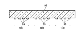
- FIG. 2 is a cross-sectional view showing the organic EL display device 100 manufactured using the vapor deposition device 90 of FIG.
- the organic EL display device 100 may include an organic EL substrate 92 and a vapor deposition layer 99 including a vapor deposition material 98 provided in a pattern.
- the plurality of vapor deposition layers 99 included in one organic EL display device 100 pass through the plurality of first holes 32 of one second mask 30 located in one opening 22 of the first mask 20, and the organic EL substrate 92. It is composed of a vapor deposition material attached to the substrate.
- the organic EL display device 100 of FIG. 2 In the organic EL display device 100 of FIG. 2, electrodes for applying a voltage to the deposition layer 99 and the like are omitted. After the vapor deposition step of forming the vapor deposition layer 99 on the organic EL substrate 92 in a pattern, the organic EL display device 100 of FIG. 2 may further include other components of the organic EL display device. Therefore, the organic EL display device 100 in FIG. 2 can also be called an intermediate of the organic EL display device.
- the vapor deposition devices 90 each having the mask device 10 corresponding to each color are prepared, and the organic EL substrate 92 is sequentially put into each vapor deposition device 90.
- an organic light emitting material for red, an organic light emitting material for green, and an organic light emitting material for blue can be sequentially deposited on the organic EL substrate 92.
- the vapor deposition process may be performed inside the vapor deposition device 90 in a high temperature atmosphere.
- the first mask 20, the second mask 30, the frame 15, and the organic EL substrate 92 held inside the vapor deposition apparatus 90 are also heated during the vapor deposition process.
- the first mask 20, the second mask 30, the frame 15, and the organic EL substrate 92 exhibit a dimensional change behavior based on their respective thermal expansion coefficients.
- the thermal expansion coefficients of the first mask 20, the second mask 30, and the frame 15 are equivalent to the thermal expansion coefficient of the organic EL substrate 92.
- an iron alloy containing nickel can be used as a main material of the first mask 20, the second mask 30, and the frame 15.
- an iron alloy containing 30% by mass or more and 54% by mass or less of nickel can be used as a material of a plate member constituting the first mask 20 and the second mask 30.
- the iron alloy containing nickel examples include an invar material containing 34% by mass or more and 38% by mass or less of nickel, a super invar material containing 30% by mass or more and 34% by mass or less of nickel in addition to cobalt, 38 Low thermal expansion Fe—Ni-based plating alloys containing not less than 54% by mass and not more than 54% by mass of nickel can be exemplified.
- the first mask 20 and the second mask 30 may be made of a material other than the above-described iron alloy.
- an iron alloy other than the above-described iron alloy containing nickel such as an iron alloy containing chromium
- an iron alloy called so-called stainless steel can be used.
- an alloy other than an iron alloy such as nickel or a nickel-cobalt alloy may be used.
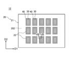
- FIG. 3 is a plan view showing the first mask 20.
- the plurality of openings 22 of the first mask 20 are arranged along the first direction D1 and the second direction D2, as shown in FIG.
- Both the first direction D1 and the second direction D2 are directions parallel to the surface direction of the plate member 21 of the first mask 20.
- the second direction D2 is orthogonal to the first direction D1.
- One opening 22 of the first mask 20 corresponds to a display area of one organic EL display device 100.
- multi-sided deposition of the organic EL display device 100 becomes possible.
- FIG. 4 is a plan view showing a plurality of second masks 30.
- the plurality of second masks 30 are arranged at a pitch corresponding to the plurality of openings 22 of the first mask 20.
- One second mask 30 corresponds to a display area of one organic EL display device 100.
- Each second mask 30 includes a metal layer 31 and a plurality of first holes 32 penetrating the metal layer 31.
- the metal layer 31 includes, for example, a plating layer formed by a plating process.
- FIG. 4 shows an example in which the plurality of first holes 32 are arranged in the first direction D1 and the second direction D2 as in the case of the first mask 20, but the arrangement of the first holes 32 is shown.
- the direction is not particularly limited.
- the plurality of first holes 32 may be arranged in a direction inclined with respect to the first direction D1 and the second direction D2.
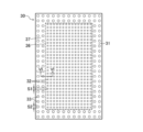
- FIG. 5 is a plan view showing the second mask 30 in an enlarged manner.
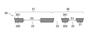
- FIG. 6 is a cross-sectional view of the second mask 30 of FIG. 5 taken along line VI-VI.
- the second mask 30 has an effective area 36 including the plurality of first holes 32 described above, and a peripheral area 37 located on the periphery of the effective area 36.
- the outline of the effective area 36 has a substantially quadrangular shape in plan view, and more precisely a substantially rectangular shape in plan view.
- the effective area 36 can have various contours according to the shape of the display area of the organic EL substrate 92.
- the outline of the effective area 36 may have a circular shape.
- the peripheral region 37 is a region where a bonding portion 40 described later for bonding the first mask 20 and the second mask 30 is provided.
- the second mask 30 includes a third surface 301 and a fourth surface 302 located on the opposite side of the third surface 301.
- the third surface 301 is located on the first surface 201 side of the first mask 20, and the fourth surface 302 is located on the second surface 202 side of the first mask 20. That is, as in the case of the first mask 20, the third surface 301 of the second mask 30 is a surface facing the organic EL substrate 92, and the fourth surface 302 is a surface located on the side of the evaporation source.
- FIG. 5 described above is a plan view illustrating a case where the second mask 30 is viewed from the fourth surface 302 side.
- the peripheral region 37 of the second mask 30 may include a plurality of second holes 33 that are recessed from the fourth surface 302 of the second mask 30 to the third surface 301.
- the second hole 33 is a hole into which a bonding portion 40 described later enters. The contact area between the second mask 30 and the joint 40 can be increased by allowing the joint 40 to enter the second hole 33.
- the second hole 33 in the peripheral region 37 penetrates from the fourth surface 302 side of the second mask 30 to the third surface 301 side.
- the second hole 33 does not have to penetrate to the third surface 301 side.
- the first hole 32 has a shape corresponding to the deposition layer 99 formed on the organic EL substrate 92 in a plan view.
- the shape of the first hole 32 has a circular shape in plan view.
- the first hole 32 may have another shape such as an ellipse or a polygon.
- the second hole 33 is a hole into which a bonding portion 40 described later enters.
- the joint 40 includes a plating layer formed by a plating process, as described later.
- the second holes 33 are configured so that the plating solution easily enters the second holes 33 during the plating process.
- the size S2 of the second hole 33 is preferably larger than the size S1 of the first hole 32.
- the dimension S2 of the second hole 33 may be smaller than the dimension S1 of the first hole 32.
- the dimension S2 of the second hole 33 may be the same as the dimension S1 of the first hole 32.
- the size S1 of the first hole 32 is determined based on the pixel density of the organic EL substrate 92 and the like.
- the dimension S1 of the first hole 32 is, for example, not less than 10 ⁇ m and not more than 60 ⁇ m.
- the dimensions, width, length, thickness, and the like of the first hole 32 and other components of the mask 12 are calculated based on a cross-sectional image of the mask 12 obtained using a scanning microscope, unless otherwise specified. .
- the dimension S2 of the second hole 33 may be 10 ⁇ m or more, 20 ⁇ m or more, 30 ⁇ m or more, or 40 ⁇ m or more.
- the dimension S ⁇ b> 2 of the second hole 33 may be 200 ⁇ m or less, 150 ⁇ m or less, 120 ⁇ m or less, or 100 ⁇ m or less.
- the number of the second holes 33 in the peripheral region 37 can be increased, and the contact area between the second mask 30 and the joint 40 can be increased. .
- the range of the dimension S2 of the second hole 33 may be determined by a combination of any one of the above-mentioned plurality of upper limit candidate values and any one of the above-mentioned plurality of lower limit candidate values.
- the range of the dimension S2 of the second hole 33 may be 10 ⁇ m to 200 ⁇ m, may be 20 ⁇ m to 150 ⁇ m, may be 30 ⁇ m to 120 ⁇ m, and may be 40 ⁇ m to 100 ⁇ m. Is also good.
- the range of the dimension S2 of the second hole 33 may be determined by a combination of any two of the plurality of lower limit candidate values described above.
- the range of the size S2 of the second hole 33 may be 10 ⁇ m to 30 ⁇ m, may be 10 ⁇ m to 20 ⁇ m, may be 20 ⁇ m to 40 ⁇ m, and may be 20 ⁇ m to 30 ⁇ m. Is also good.
- the range of the dimension S2 of the second hole 33 may be determined by a combination of any two of the plurality of upper limit candidate values described above.
- the range of the dimension S2 of the second hole 33 may be 100 ⁇ m or more and 150 ⁇ m or less, 100 ⁇ m or more and 120 ⁇ m or less, 120 ⁇ m or more and 200 ⁇ m or less, or 150 ⁇ m or more and 200 ⁇ m or less. Is also good.
- the shape of the second hole 33 in a plan view is a shape that can easily prevent the joint 40 from being separated from the second hole 33 of the second mask 30 on the fourth surface 302 side of the second mask 30. You may.
- the second hole 33 may include a corner having an interior angle of less than 90 degrees.
- the shape of the second hole 33 may be a triangle, a star, or a parallelogram.
- a plurality of, for example, two second holes 33 are arranged in a direction from the boundary between the effective area 36 and the peripheral area 37 to the outer edge of the peripheral area 37.
- the method of arranging the second holes 33 is not particularly limited.
- one second hole 33 may exist in a direction from a boundary between the effective region 36 and the peripheral region 37 to an outer edge of the peripheral region 37.
- three or more second holes 33 may be arranged in a direction from a boundary between the effective region 36 and the peripheral region 37 to an outer edge of the peripheral region 37.
- the first hole 32 may include a portion where the dimension S1 increases from the third surface 301 side to the fourth surface 302 side. Thereby, it is possible to suppress the occurrence of shadow in the vapor deposition step.
- the shape of the first hole 32 in the sectional view is not limited to the shape shown in FIG.
- the dimension S2 of the second hole 33 is the same on the third surface 301 side and the fourth surface 302 side.
- the second hole 33 may include a portion where the dimension S2 increases from the third surface 301 side to the fourth surface 302 side, like the first hole 32.
- the second hole 33 may include a portion in which the dimension S2 decreases from the third surface 301 side to the fourth surface 302 side. Thereby, it becomes easy to suppress that the bonding part 40 is separated from the second hole 33 of the second mask 30 on the fourth surface 302 side of the second mask 30.
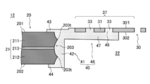
- FIG. 7 is a plan view showing a case where the mask 12 including the first mask 20 and the second mask 30 is viewed from the second surface 202 side.
- the mask 12 includes a first mask 20 including a plurality of openings 22 and a plurality of second masks 30 respectively located in the plurality of openings 22 of the first mask 20.
- the mask 12 further includes a bonding portion 40 for bonding the first mask 20 and the second mask 30.
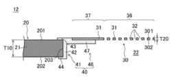
- FIG. 8 is a cross-sectional view of the mask 12 of FIG. 7 taken along the line VIII-VIII.
- the plate member 21 of the first mask 20 has a side surface 203 extending from the first surface 201 to the second surface 202.
- the opening 22 described above is defined by the side surface 203.
- reference numeral T10 indicates the thickness of the plate member 21 of the first mask 20
- reference numeral T20 indicates the thickness of the metal layer 31 of the second mask 30.
- the thickness T10 of the plate member 21 may be, for example, 200 ⁇ m or more, 300 ⁇ m or more, 400 ⁇ m or more, or 500 ⁇ m or more.
- the thickness T10 of the plate member 21 may be, for example, 1000 ⁇ m or less, 800 ⁇ m or less, 700 ⁇ m or less, or 600 ⁇ m or less.
- the range of the thickness T10 of the plate member 21 may be determined by a combination of any one of the above-described plurality of lower limit candidate values and any one of the above-described plurality of upper limit candidate values.
- the range of the thickness T10 of the plate member 21 may be determined by a combination of any two of the plurality of lower limit candidate values described above, and may be, for example, 200 ⁇ m or more and 500 ⁇ m or less, or 200 ⁇ m or more and 400 ⁇ m or less. Or less, may be 300 ⁇ m or more and 500 ⁇ m or less, or may be 300 ⁇ m or more and 400 ⁇ m or less.
- the range of the thickness T10 of the plate member 21 may be determined by a combination of any two of the plurality of upper limit candidate values described above, and may be, for example, from 600 ⁇ m to 1000 ⁇ m, or from 600 ⁇ m to 800 ⁇ m. Or less, 700 ⁇ m or more and 1000 ⁇ m or less, or 700 ⁇ m or more and 800 ⁇ m or less.
- the thickness T20 of the metal layer 31 may be, for example, 4 ⁇ m or more, 5 ⁇ m or more, 7 ⁇ m or more, or 10 ⁇ m or more.
- the thickness T20 of the metal layer 31 may be, for example, 20 ⁇ m or less, 18 ⁇ m or less, 15 ⁇ m or less, or 12 ⁇ m or less.
- the range of the thickness T20 of the metal layer 31 may be determined by a combination of any one of the above plurality of lower limit candidate values and any one of the above plurality of upper limit candidate values.
- the range of the thickness T20 of the metal layer 31 may be determined by a combination of any two of the plurality of lower limit candidate values described above, and may be, for example, 4 ⁇ m or more and 10 ⁇ m or less, or 4 ⁇ m or more and 7 ⁇ m or less. Or less, 5 ⁇ m or more and 10 ⁇ m or less, or 5 ⁇ m or more and 7 ⁇ m or less.
- the range of the thickness T20 of the metal layer 31 may be determined by a combination of any two of the plurality of upper limit candidate values described above, and may be, for example, from 12 ⁇ m to 20 ⁇ m, or from 12 ⁇ m to 18 ⁇ m. Or less, 15 ⁇ m or more and 20 ⁇ m or less, or 15 ⁇ m or more and 18 ⁇ m or less.
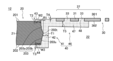
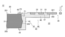
- the bonding portion 40 includes a first portion 41 that is in contact with the first mask 20, and a second portion 46 that is integrally formed with the first portion 41 and is in contact with the peripheral region 37 of the second mask 30.
- the first portion 41 includes at least a side surface portion 42 and a first surface portion 43.
- the side surface portion 42 is a portion of the first portion 41 that is in contact with the side surface 203 of the first mask 20.
- the first surface portion 43 is a portion of the first portion 41 that is in contact with the first surface 201 of the first mask 20.
- the first portion 41 is in contact with the first mask 20 on two surfaces, the side surface 203 and the first surface 201 of the first mask 20, so that when a force is externally applied to the mask 12, the first mask 20 and the joint 40 Can be dispersed in a plurality of directions. Thereby, it is possible to suppress the first portion 41 from being separated from the first mask 20.
- the first portion 41 may further include a second surface portion 44 that is in contact with the second surface 202 of the first mask 20.
- the second portion 46 includes at least a fourth surface portion 47 that is in contact with the fourth surface 302 of the peripheral region 37 of the second mask 30.
- the second portion 46 may further include a hole portion 48 located inside the second hole 33. Since the second portion 46 includes the hole portion 48, the contact area between the peripheral region 37 of the second mask 30 and the second portion 46 of the joint 40 can be increased. Thereby, it is possible to suppress the second portion 46 from being separated from the peripheral region 37 of the second mask 30.
- FIG. 9 is a cross-sectional view showing the mask 12 of FIG. 8 in an enlarged manner.
- the side surface 203 of the first mask 20 may have a protruding portion 203 t protruding toward the second mask 30 located in the opening 22.
- a protruding portion 203t may be generated when the opening 22 is formed in the plate member 21 by wet etching the plate member 21 from both the first surface 201 side and the second surface 202 side, as described later. Since the side surface 203 of the first mask 20 has such a protruding portion 203t, the side surface portion 42 of the first portion 41 of the bonding portion 40 and the side surface of the first mask 20 are compared with the case where the side surface 203 is a flat surface.
- the contact area between the first and second contacts 203 can be increased. Thereby, it is possible to prevent the first portion 41 of the joint portion 40 from being separated from the side surface 203 of the first mask 20. Further, the anchor effect of the projecting portion 203t of the side surface 203 of the first mask 20 with respect to the side surface portion 42 of the first portion 41 of the joint portion 40 also shows that the first portion 41 is separated from the side surface 203 of the first mask 20. It can work to suppress.
- reference numeral R1 denotes a protruding length of the protruding portion 203t of the side surface 203 with respect to the first surface 201.
- the protrusion length R1 of the protrusion 203t may be, for example, 10 ⁇ m or more, 20 ⁇ m or more, 30 ⁇ m or more, or 40 ⁇ m or more.
- the anchor effect can be enhanced by increasing the protrusion length R1 of the protrusion 203t.
- the protrusion length R1 of the protrusion 203t may be 100 ⁇ m or less, 80 ⁇ m or less, 65 ⁇ m or less, or 50 ⁇ m or less.
- the range of the protrusion length R1 of the protrusion 203t may be determined by a combination of any one of the plurality of lower limit candidate values and any one of the plurality of upper limit candidate values. For example, it may be 10 ⁇ m or more and 100 ⁇ m or less, 20 ⁇ m or more and 80 ⁇ m or less, 30 ⁇ m or more and 65 ⁇ m or less, or 40 ⁇ m or more and 50 ⁇ m or less. Further, the range of the protruding length R1 of the protruding portion 203t may be determined by an arbitrary combination of two of the above-described plurality of lower limit candidate values, and may be, for example, 10 ⁇ m or more and 40 ⁇ m or less, or 10 ⁇ m or more.
- the range of the protruding length R1 of the protruding portion 203t may be determined by a combination of any two of the above-described plurality of upper limit candidate values, and may be, for example, 50 ⁇ m or more and 100 ⁇ m or less, or 50 ⁇ m or more. It may be 80 ⁇ m or less, 65 ⁇ m or more and 100 ⁇ m or less, 65 ⁇ m or more and 80 ⁇ m or less, or 80 ⁇ m or more and 100 ⁇ m or less.
- the side surface 203 of the first mask 20 includes a rough surface 203s having irregularities.
- the side surface portion 42 of the first portion 41 of the bonding portion 40 can enter the unevenness of the rough surface 203s of the side surface 203, the adhesion of the side surface portion 42 of the bonding portion 40 to the side surface 203 of the first mask 20 is improved. Can be even higher. Thereby, it is possible to prevent the first portion 41 of the joint portion 40 from being separated from the side surface 203 of the first mask 20.
- the surface roughness of the rough surface 203s of the side surface 203 is the arithmetic average roughness Sa.
- the arithmetic average roughness of the rough surface 203s is calculated by using a measuring instrument based on ISO25178.
- the arithmetic average roughness of the rough surface 203s may be 0.12 ⁇ m or more, 0.14 ⁇ m or more, 0.17 ⁇ m or more, or 0.19 ⁇ m or more.
- the anchor effect can be increased by increasing the arithmetic average roughness of the rough surface 203s of the side surface 203.
- the arithmetic average roughness of the rough surface 203s may be 0.28 ⁇ m or less, 0.25 ⁇ m or less, 0.23 ⁇ m or less, or 0.21 ⁇ m or less. Good.
- the range of the arithmetic average roughness of the rough surface 203s is determined by a combination of any one of the plurality of lower limit candidate values and any one of the plurality of upper limit candidate values. For example, it may be from 0.12 ⁇ m to 0.28 ⁇ m, from 0.14 ⁇ m to 0.25 ⁇ m, from 0.17 ⁇ m to 0.23 ⁇ m, and from 0.19 ⁇ m It may be not less than 0.21 ⁇ m.
- the range of the arithmetic average roughness of the rough surface 203s may be determined by a combination of any two of the above-described plurality of lower limit candidate values, for example, 0.12 ⁇ m or more and 0.19 ⁇ m or less.
- the range of the arithmetic average roughness of the rough surface 203s may be determined by a combination of any two of the above-described plurality of upper limit candidate values, and is, for example, 0.21 ⁇ m or more and 0.28 ⁇ m or less.
- reference symbol T1 represents the thickness of the side surface portion 42 of the first portion 41 of the bonding portion 40 located on the side surface 203 of the first mask 20.
- the symbol T2 indicates the thickness of the first surface portion 43 of the first portion 41 of the bonding portion 40 located on the first surface 201 of the first mask 20.
- Reference symbol T3 represents the thickness of the second surface portion 44 of the first portion 41 of the bonding portion 40 located on the second surface 202 of the first mask 20.
- the thickness T1 of the side surface portion 42 may be, for example, 20 ⁇ m or more, 30 ⁇ m or more, 40 ⁇ m or more, or 50 ⁇ m or more.
- the thickness T1 of the side surface portion 42 may be, for example, 110 ⁇ m or less, 90 ⁇ m or less, 70 ⁇ m or less, or 60 ⁇ m or less.
- the range of the thickness T1 of the side surface portion 42 may be determined by a combination of any one of the plurality of lower limit candidate values and any one of the plurality of upper limit candidate values.
- the range of the thickness T1 of the side surface portion 42 may be determined by an arbitrary combination of two of the plurality of lower limit candidate values described above, and may be, for example, 20 ⁇ m or more and 50 ⁇ m or less, or 20 ⁇ m or more and 40 ⁇ m or less. Or less, may be 30 ⁇ m or more and 50 ⁇ m or less, or may be 30 ⁇ m or more and 40 ⁇ m or less.
- the range of the thickness T1 of the side surface portion 42 may be determined by a combination of any two of the above-described plurality of upper limit candidate values, and may be, for example, from 60 ⁇ m to 110 ⁇ m, or from 60 ⁇ m to 90 ⁇ m. Or less, 70 ⁇ m or more and 110 ⁇ m or less, or 70 ⁇ m or more and 90 ⁇ m or less.
- the thickness T2 of the first surface portion 43 may be, for example, 3 ⁇ m or more, 5 ⁇ m or more, 7 ⁇ m or more, or 10 ⁇ m or more.
- the thickness T2 of the first surface portion 43 may be, for example, 30 ⁇ m or less, 25 ⁇ m or less, 20 ⁇ m or less, or 15 ⁇ m or less.
- the range of the thickness T2 of the first surface portion 43 may be determined by a combination of any one of the plurality of lower limit candidate values and any one of the plurality of upper limit candidate values.
- the thickness may be 3 ⁇ m or more and 30 ⁇ m or less, 5 ⁇ m or more and 25 ⁇ m or less, 7 ⁇ m or more and 20 ⁇ m or less, or 10 ⁇ m or more and 15 ⁇ m or less.
- the range of the thickness T2 of the first surface portion 43 may be determined by a combination of any two of the plurality of lower limit candidate values described above, and may be, for example, 3 ⁇ m or more and 10 ⁇ m or less, or 3 ⁇ m. It may be not less than 7 ⁇ m, not less than 5 ⁇ m and not more than 10 ⁇ m, or not less than 5 ⁇ m and not more than 7 ⁇ m.
- the range of the thickness T2 of the first surface portion 43 may be determined by a combination of any two of the above plurality of upper limit candidate values, and may be, for example, 15 ⁇ m or more and 30 ⁇ m or less, or 15 ⁇ m or less. It may be not less than 25 ⁇ m, not less than 20 ⁇ m and not more than 30 ⁇ m, or not less than 20 ⁇ m and not more than 25 ⁇ m.
- the thickness T3 of the second surface portion 44 may be, for example, 30 ⁇ m or more, 40 ⁇ m or more, 50 ⁇ m or more, or 60 ⁇ m or more.
- the thickness T3 of the second surface portion 44 may be, for example, 150 ⁇ m or less, 120 ⁇ m or less, 90 ⁇ m or less, or 70 ⁇ m or less.
- the range of the thickness T3 of the second surface portion 44 may be determined by a combination of any one of the plurality of lower limit candidate values and any one of the plurality of upper limit candidate values.
- the range of the thickness T3 of the second surface portion 44 may be determined by a combination of any two of the plurality of lower limit candidate values described above, and may be, for example, 30 ⁇ m or more and 60 ⁇ m or less, or 30 ⁇ m or less. It may be not less than 50 ⁇ m, not less than 40 ⁇ m and not more than 60 ⁇ m, or not less than 40 ⁇ m and not more than 50 ⁇ m.
- the range of the thickness T3 of the second surface portion 44 may be determined by a combination of any two of the plurality of upper limit candidate values described above, and may be, for example, 70 ⁇ m or more and 150 ⁇ m or less, or 70 ⁇ m or less. It may be not less than 120 ⁇ m, not less than 90 ⁇ m and not more than 150 ⁇ m, or not less than 90 ⁇ m and not more than 120 ⁇ m.
- the surface of the first surface portion 43 of the first portion 41 of the joint 40 may be located on the same plane as the third surface 301 of the second mask 30.
- the surface of the first surface portion 43 is made to infiltrate a plating solution between a substrate 65 which will be described later, which serves as a base for manufacturing the second mask 30 by plating, and the first surface 201 of the first mask 20. This may occur when the first surface portion 43 is formed.
- “on the same plane” refers to not only the case where the distance T4 between the surface of the first surface portion 43 and the third surface 301 of the second mask 30 in the thickness direction of the second mask 30 is zero, but also the distance.
- the concept includes a case where T4 is 15 ⁇ m or less, a case where it is 10 ⁇ m or less, and a case where T4 is 5 ⁇ m or less.
- the symbol T5 indicates the thickness of the fourth surface portion 47 of the second portion 46 of the joint 40 located on the fourth surface 302 of the second mask 30.
- the thickness T5 of the fourth surface portion 47 may be, for example, 30 ⁇ m or more, 40 ⁇ m or more, 50 ⁇ m or more, or 60 ⁇ m or more.
- the thickness T5 of the fourth surface portion 47 may be, for example, 150 ⁇ m or less, 120 ⁇ m or less, 90 ⁇ m or less, or 70 ⁇ m or less.
- the range of the thickness T5 of the fourth surface portion 47 may be determined by a combination of any one of the plurality of lower limit candidate values and any one of the plurality of upper limit candidate values.
- the thickness T5 of the fourth surface portion 47 may be determined by a combination of any two of the plurality of lower limit candidate values described above, and may be, for example, 30 ⁇ m or more and 60 ⁇ m or less, or 30 ⁇ m or less. It may be not less than 50 ⁇ m, not less than 40 ⁇ m and not more than 60 ⁇ m, or not less than 40 ⁇ m and not more than 50 ⁇ m.
- the range of the thickness T5 of the fourth surface portion 47 may be determined by a combination of any two of the above-described plurality of upper limit candidate values, and may be, for example, 70 ⁇ m or more and 150 ⁇ m or less, or 70 ⁇ m or less. It may be not less than 120 ⁇ m, not less than 90 ⁇ m and not more than 150 ⁇ m, or not less than 90 ⁇ m and not more than 120 ⁇ m. Further, as shown in FIG. 9, the fourth surface portion 47 may include a portion where the thickness T5 increases from the first mask 20 side to the second mask 30 side.
- reference symbol W2 represents the width of the first surface portion 43 of the first portion 41 of the joint 40.
- the width W2 of the first surface portion 43 is the width W2 from the end of the first surface 201 of the first mask 20 on the opening 22 side to the end of the first surface portion 43 of the first portion 41 of the joint 40. This is the distance in the in-plane direction of the first surface 201 of one mask 20.
- the width W2 of the first surface portion 43 may be 3 ⁇ m or more, 5 ⁇ m or more, 7 ⁇ m or more, or 10 ⁇ m or more.
- the width W2 of the first surface portion 43 may be 500 ⁇ m or less, 250 ⁇ m or less, 100 ⁇ m or less, or 30 ⁇ m or less.
- the range of the width W2 of the first surface portion 43 may be determined by a combination of any one of the plurality of lower limit candidate values and any one of the plurality of upper limit candidate values. For example, it may be 3 ⁇ m or more and 500 ⁇ m or less, 5 ⁇ m or more and 250 ⁇ m or less, 7 ⁇ m or more and 100 ⁇ m or less, or 10 ⁇ m or more and 30 ⁇ m or less.
- the range of the width W2 of the first surface portion 43 may be determined by a combination of any two of the plurality of lower limit candidate values described above, and may be, for example, 3 ⁇ m or more and 10 ⁇ m or less, or 3 ⁇ m or less.
- the range of the width W2 of the first surface portion 43 may be determined by a combination of any two of the plurality of upper limit candidate values described above, and may be, for example, 30 ⁇ m or more and 500 ⁇ m or less, or 30 ⁇ m or less. It may be 250 ⁇ m or less, 100 ⁇ m or more and 500 ⁇ m or less, 100 ⁇ m or more and 250 ⁇ m or less, or 250 ⁇ m or more and 500 ⁇ m or less.
- reference symbol W3 represents the width of the second surface portion 44 of the first portion 41 of the joint 40.
- the width W3 of the second surface portion 44 is the width W3 from the end of the second surface 202 of the first mask 20 on the opening 22 side to the end of the second surface portion 44 of the first portion 41 of the joint 40.
- the width W3 of the second surface portion 44 may be 3 ⁇ m or more, 5 ⁇ m or more, 7 ⁇ m or more, or 10 ⁇ m or more.
- the width W3 of the second surface portion 44 may be smaller than the width of the second surface 202, for example, may be 80 ⁇ m or less, may be 60 ⁇ m or less, may be 40 ⁇ m or less, It may be 20 ⁇ m or less.
- the range of the width W3 of the second surface portion 44 may be determined by a combination of any one of the plurality of lower limit candidate values and any one of the plurality of upper limit candidate values. For example, it may be 3 ⁇ m to 80 ⁇ m, may be 5 ⁇ m to 60 ⁇ m, may be 7 ⁇ m to 60 ⁇ m, may be 7 ⁇ m to 40 ⁇ m, and may be 10 ⁇ m to 20 ⁇ m. Is also good.
- the range of the width W3 of the second surface portion 44 may be determined by a combination of any two of the plurality of lower limit candidate values described above, and may be, for example, 3 ⁇ m or more and 10 ⁇ m or less, or 3 ⁇ m It may be not less than 7 ⁇ m, not less than 3 ⁇ m and not more than 5 ⁇ m, not less than 5 ⁇ m and not more than 10 ⁇ m, or not less than 5 ⁇ m and not more than 7 ⁇ m. Further, the range of the width W3 of the second surface portion 44 may be determined by a combination of any two of the plurality of upper limit candidate values described above, and may be, for example, 20 ⁇ m or more and 80 ⁇ m or less, or 20 ⁇ m or less. It may be not less than 60 ⁇ m, not less than 40 ⁇ m and not more than 80 ⁇ m, not less than 40 ⁇ m and not more than 60 ⁇ m, or not less than 60 ⁇ m and not more than 80 ⁇ m.
- the method of manufacturing the mask 12 includes a first mask preparation step of preparing the first mask 20, a second mask preparation step of preparing the second mask 30, and a bonding part for bonding the first mask 20 and the second mask 30. And a bonding part forming step of forming the bonding part 40. Note that the order of the first mask preparation step and the second mask preparation step is arbitrary.
- the first mask preparation step will be described with reference to FIGS.
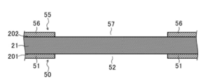
- a plate member 21 made of metal is prepared.
- the plate member 21 has, for example, an iron alloy containing 30% by mass or more and 38% by mass or less of nickel.
- a first surface resist pattern 50 is provided on the first surface 201 of the plate member 21, and a second surface resist pattern 55 is provided on the second surface 202.
- the first surface resist pattern 50 includes a first surface resist layer 51 and an opening 52 formed in the first surface resist layer 51.
- the second surface resist pattern 55 includes a second surface resist layer 56 and an opening 57. The opening 52 and the opening 57 are located in a portion of the plate member 21 where the opening 22 is formed.
- first surface resist layer 51 and the second surface resist layer 56 for example, a dry film containing a photosensitive resist material such as an acrylic photocurable resin is attached to the first surface 201 and the second surface 202 of the plate member 21. Obtained by: The first-side resist layer 51 and the second-side resist layer 56 are formed by applying a coating solution containing a negative photosensitive resist material on the first surface 201 and the second surface 202 of the plate member 21. May be obtained by drying. The opening 52 and the opening 57 are formed by exposing and developing the first surface resist layer 51 and the second surface resist layer 56.
- a photosensitive resist material such as an acrylic photocurable resin
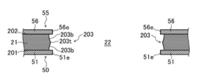
- the plate member 21 is wet-etched from the first surface 201 side and the second surface 202 side using the first surface resist pattern 50 and the second surface resist pattern 55 as a mask.
- the opening 22 can be formed in the plate member 21 as shown in FIG. it can.
- a protrusion 203t may be formed at a position of the side surface 203 of the plate member 21 where the concave portion on the first surface 201 side and the concave portion on the second surface 202 merge.
- a sandblasting step of performing sandblasting on the side surface 203 of the first mask 20 may be performed. Thereby, a rough surface 203s can be formed on the side surface 203 of the first mask 20.
- the sandblasting process may be performed in a state where the first surface resist pattern 50 and the second surface resist pattern 55 are provided on the plate member 21.
- the first surface resist pattern 50 protrudes toward the opening 22 from the end of the first surface 201
- the second surface resist pattern 55 similarly has the second surface 202. It protrudes toward the opening 22 side from the end. Therefore, the arrival of the polishing agent B such as sand on the side surface 203 of the first mask 20 can be hindered by the first surface resist pattern 50 and the second surface resist pattern 55.
- the polishing agent B such as sand on the side surface 203 of the first mask 20
- a first surface resist layer 53 and a second surface resist layer 58 different from the first surface resist layer 51 and the second surface resist layer 56 used in wet etching may be performed in a state where is provided on the first surface 201 and the second surface 202 of the plate member 21.
- the end 53e of the first surface resist layer 53 does not protrude toward the opening 22 compared to the protrusion 203t of the side surface 203 of the first mask 20.
- the end 58 e of the second surface resist layer 58 does not protrude toward the opening 22 than the protrusion 203 t on the side surface 203 of the first mask 20. Accordingly, it is possible to suppress the arrival of the abrasive B such as sand from reaching the side surface 203 of the first mask 20 by the first surface resist layer 53 and the second surface resist layer 58.
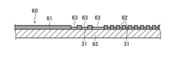
- the substrate 65 is prepared. At least the surface of the substrate 65 is preferably made of a conductive material.
- the substrate 65 includes stainless steel or the like.
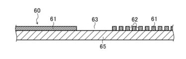
- a first resist pattern 60 is formed on the surface of the substrate 65.
- the first resist pattern 60 has a first resist layer 61, and a plurality of first openings 62 and a plurality of second openings 63 formed in the first resist layer 61.
- the first opening 62 is provided in a portion of the substrate 65 where the metal layer 31 is to be formed in the effective area 36 of the second mask 30.
- the second opening 63 is provided in a portion of the substrate 65 where the metal layer 31 is to be formed in the peripheral region 37 of the second mask 30.
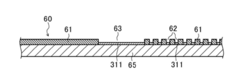
- a plating solution is supplied onto the substrate 65.
- the metal layer 31 made of the plating layer generated by the electrolytic plating can be formed in the first opening 62 and the second opening 63 of the first resist layer 61.
- the plating solution contains, for example, nickel sulfamate and nickel bromide. Further, the plating solution may further contain ferrous sulfamate and the like.
- the first resist pattern 60 is removed.
- the second mask 30 having the plurality of first holes 32 and the second holes 33 can be formed on the substrate 65.
- a photosensitive layer 71 covering the second mask 30 and the substrate 65 is formed on the substrate 65 on which the second mask 30 is provided.
- the photosensitive layer 71 may be obtained by attaching a dry film containing a photosensitive resist material to the substrate 65, as in the case of the above-described first surface resist layer 51. Further, the photosensitive layer 71 may be obtained by applying a coating liquid containing a negative photosensitive resist material on the substrate 65 and drying the coating liquid.
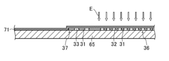
- an exposure step of irradiating light to a portion of the photosensitive layer 71 located on the effective area 36 of the second mask 30 is performed.
- a portion of the photosensitive layer 71 located on the peripheral region 37 of the second mask 30 is not irradiated with light.
- light is not irradiated on a portion of the photosensitive layer 71 located on the substrate 65 at the periphery of the second mask 30.
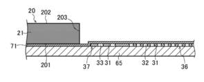
- the first mask 20 is arranged on the photosensitive layer 71 on the substrate 65 so that the second mask 30 is located in the opening 22 of the first mask 20.
- a developing step of developing the photosensitive layer 71 is performed.
- a portion of the photosensitive layer 71 located on the peripheral region 37 of the second mask 30 is removed.
- a portion of the photosensitive layer 71 located between the first surface 201 of the first mask 20 and the substrate 65 and near the side surface 203 of the first mask 20 is removed.
- the developer does not reach or hardly reaches the portion of the photosensitive layer 71 located between the first surface 201 of the first mask 20 and the substrate 65, which is away from the side surface 203 of the first mask 20. . Therefore, as shown in FIG. 18, the unexposed photosensitive layer 71 partially remains between the first surface 201 of the first mask 20 and the substrate 65.
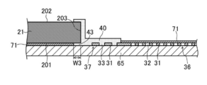
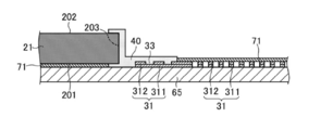
- a plating process is performed in which a plating solution is supplied onto the substrate 65 to form the joint 40.
- the plating solution contacts the side surface 203 of the first mask 20 and the peripheral region 37 of the second mask 30, and the photosensitive layer 71 between the first surface 201 of the first mask 20 and the substrate 65 is formed.
- the plating solution enters the removed space.
- the plating solution that has entered the space from which the photosensitive layer 71 has been removed becomes the first surface portion 43 of the first portion 41 of the joint 40.
- the plating solution remaining on the second surface 202 of the plate member 21 becomes the second surface portion 44 of the first portion 41 of the joint 40.
- a resist layer may be provided on a portion of the second surface 202 of the plate member 21 where the second surface portion 44 should not be formed before performing the plating process. Thereby, the width W3 of the second surface portion 44 formed on the second surface 202 of the plate member 21 can be controlled.
- the amount of the photosensitive layer 71 removed between the first surface 201 of the first mask 20 and the substrate 65 is adjusted by adjusting the time of a developing step for developing the photosensitive layer 71. can do. Thereby, the width W2 of the first surface portion 43 formed by the plating solution entering the space from which the photosensitive layer 71 has been removed can be adjusted.
- the photosensitive layer 71 is removed.
- the first mask 20, the second mask 30, and the bonding portion 40 are separated from the substrate 65. In this way, it is possible to obtain the mask 12 including the first mask 20 and the second mask 30, and the joint 40 that joins the first mask 20 and the second mask 30.
- the order of the exposure step of irradiating light to the portion of the photosensitive layer 71 located on the effective area 36 of the second mask 30 and the arrangement step of arranging the first mask 20 on the photosensitive layer 71 are arbitrary. That is, the arrangement step may be performed after the exposure step, or the exposure step may be performed after the arrangement step.
- FIG. 16 shows an example in which the photosensitive layer 71 is of a photo-curable type that is cured by being irradiated with light, but is not limited thereto.
- the configuration of the photosensitive layer 71 and the configuration of the exposure process are such that a portion of the photosensitive layer 71 located on the effective area 36 of the second mask 30 remains in the subsequent development process, and the peripheral edge of the second mask 30 of the photosensitive layer 71 remains. It is optional as long as the portion located on the region 37 is removed and the portion of the photosensitive layer 71 located between the first mask 20 and the substrate 65 is partially removed.
- FIG. 20 is a diagram illustrating a state where an external force F is applied to the mask according to the comparative example.
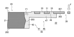
- FIG. 21 is a diagram illustrating a state where an external force F is applied to the mask 12 according to the present embodiment.
- the external force F is applied to the third surface 301 of the second mask 30 in the thickness direction of the second mask 30, for example.
- the first portion 41 of the bonding portion 40 is in contact only with the side surface 203 of the first mask 20 and is not in contact with the first surface 201.
- the first portion 41 of the joint 40 further includes the first surface portion 43.
- the force F1 is generated between the side surface portion 42 and the side surface 203 of the first portion 41, but also the first surface portion 43 and the first surface 201 of the first portion 41 .
- a force F2 is also generated. That is, the force generated between the first portion 41 of the joint 40 and the plate member 21 of the first mask 20 can be dispersed as compared with the case of the comparative embodiment shown in FIG. Thereby, it is possible to suppress the force generated between the first portion 41 of the joint portion 40 and the plate member 21 of the first mask 20 from being locally concentrated.
- separation of the first portion 41 of the joint portion 40 from the first mask 20 can be suppressed. Further, the contact area of the first portion 41 of the bonding portion 40 with the first mask 20 is increased by the amount of the first surface portion 43. Also in this regard, separation of the first portion 41 from the first mask 20 can be suppressed.
- the metal layer 31 of the second mask 30 includes one plating layer.
- the metal layer 31 may include a plurality of plating layers.
- an example in which the metal layer 31 includes two plating layers will be described with reference to FIGS.
- the first resist pattern 60 is formed on the surface of the substrate 65.
- the first resist pattern 60 includes a first resist layer 61, a plurality of first openings 62 formed in the first resist layer 61, and a second opening 63.
- the first opening 62 is provided in a portion of the substrate 65 where the metal layer 31 is to be formed in the effective region 36 of the second mask 30 as in the case of the above-described embodiment shown in FIG.
- the second opening 63 extends over the entire region of the substrate 65 corresponding to the peripheral region 37 of the second mask 30.
- a plating solution is supplied onto the substrate 65.
- the first plating layer 311 is formed in the first opening 62 and the second opening 63 of the first resist layer 61 by electrolytic plating.
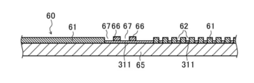
- a second resist layer 66 is formed on the first plating layer 311 formed in the second opening 63.
- An opening 67 is formed in the second resist layer 66.
- the second resist layer 66 is provided in a portion of the second mask 30 where the above-described second hole 33 is to be formed.
- a plating solution is supplied onto the substrate 65.
- the second plating layer 312 is formed in the first opening 62 of the first resist layer 61 and the opening 67 of the second resist layer 66 by electrolytic plating.
- the composition of the second plating layer 312 may be the same as or different from that of the first plating layer 311.
- the first resist layer 61 and the second resist layer 66 are removed.
- the second mask 30 having the effective region 36 including the plurality of first holes 32 and the peripheral region 37 including the plurality of second holes 33.
- the first hole 32 of the effective area 36 penetrates the metal layer 31 including the first plating layer 311 and the second plating layer 312.
- the second holes 33 in the peripheral region 37 penetrate the second plating layer 312 but do not penetrate the first plating layer 311. That is, in the present modification, the second hole 33 in the peripheral region 37 is a concave portion located on the fourth surface 302 side so as not to penetrate the metal layer 31.
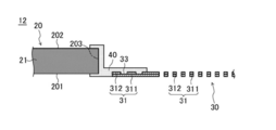
- a joint forming step for forming the joint 40 is performed as in the above-described embodiment. For example, after performing the step of forming the photosensitive layer 71 on the substrate 65, the step of exposing the photosensitive layer 71, the step of disposing the first mask 20, and the step of developing the photosensitive layer 71, as shown in FIG. Then, the bonding solution 40 is formed by supplying a plating solution onto the substrate 65. Also in the present modification, the plating solution penetrates into the second holes 33 in the peripheral region 37 of the second mask 30, so that the adhesion between the bonding portion 40 and the second mask 30 can be increased.
- the photosensitive layer 71 is removed.
- the first mask 20, the second mask 30, and the bonding portion 40 are separated from the substrate 65. In this way, as shown in FIG. 27, it is possible to obtain the mask 12 including the first mask 20 and the second mask 30, and the bonding portion 40 for bonding the first mask 20 and the second mask 30. .
- the plate member 21 of the first mask 20 has one member, but the present invention is not limited to this.
- the plate member 21 may include a plurality of members stacked in the thickness direction.
- an example in which the plate member 21 includes two members joined by an adhesive layer will be described with reference to FIG.
- FIG. 28 is a cross-sectional view showing a mask 12 according to this modification.
- the plate member 21 of the first mask 20 joins the first member 211 located on the first surface 201 side, the second member 212 located on the second surface 202 side, and the first member 211 and the second member 212.
- the adhesive layer 213 includes a resin having an adhesive property.
- the adhesive layer 213 contains an acrylic resin.
- the thickness of the adhesive layer 213 may be, for example, 3 ⁇ m or more, 5 ⁇ m or more, 7 ⁇ m or more, or 10 ⁇ m or more.
- the thickness of the adhesive layer 213 may be, for example, 40 ⁇ m or less, 30 ⁇ m or less, 20 ⁇ m or less, or 10 ⁇ m or less.
- the range of the thickness of the adhesive layer 213 may be determined by a combination of any one of the plurality of lower limit candidate values and any one of the plurality of upper limit candidate values. It may be 3 ⁇ m or more and 40 ⁇ m or less, 5 ⁇ m or more and 30 ⁇ m or less, 7 ⁇ m or more and 20 ⁇ m or less, or 10 ⁇ m or more and 10 ⁇ m or less.
- the range of the thickness of the adhesive layer 213 may be determined by a combination of any two of the plurality of lower limit candidate values described above, and may be, for example, 3 ⁇ m or more and 10 ⁇ m or less, or 3 ⁇ m or more and 7 ⁇ m or less. May be 5 ⁇ m or more and 10 ⁇ m or less, or 5 ⁇ m or more and 7 ⁇ m or less.
- the range of the thickness of the adhesive layer 213 may be determined by a combination of any two of the above plurality of upper limit candidate values, and may be, for example, 10 ⁇ m or more and 40 ⁇ m or less, or 10 ⁇ m or more and 30 ⁇ m or less. May be 20 ⁇ m or more and 40 ⁇ m or less, or may be 20 ⁇ m or more and 30 ⁇ m or less.
- the material of the first member 211 and the material of the second member 212 may be the same or different.
- each of the first member 211 and the second member 212 has an iron alloy containing 30% by mass or more and 38% by mass or less of nickel.
- the first member 211 is wet-etched from the first surface side and the second surface side to form an opening in the first member 211.
- the second member 212 is wet-etched from the first surface side and the second surface side to form an opening in the second member 212.
- the first member 211 and the second member 212 are stacked such that the opening of the first member 211 and the opening of the second member 212 overlap.
- the first mask 20 in which the openings 22 are formed can be obtained.
- Both the side surface 203 of the first member 211 and the side surface 203 of the second member 212 include a protruding portion 203t.
- the opening is formed in the member as compared with the case where the plate member 21 is formed of one member.
- the present invention is not limited to this.
- the second holes 33 may not be formed in the peripheral region 37 of the second mask 30.
- the second portion 46 of the bonding portion 40 includes the fourth surface portion 47 in contact with the fourth surface 302, the second portion 46 is separated from the peripheral region 37 of the second mask 30. Can be suppressed.
- the first portion 41 of the joint 40 includes the side surface portion 42 and the first surface portion 43, the first portion 41 of the joint 40 is generated between the first portion 41 of the joint 40 and the plate member 21 of the first mask 20.
Landscapes
- Chemical & Material Sciences (AREA)
- Engineering & Computer Science (AREA)
- Metallurgy (AREA)
- Chemical Kinetics & Catalysis (AREA)
- Materials Engineering (AREA)
- Organic Chemistry (AREA)
- Mechanical Engineering (AREA)
- Manufacturing & Machinery (AREA)
- Electrochemistry (AREA)
- General Chemical & Material Sciences (AREA)
- Electroluminescent Light Sources (AREA)
- Physical Vapour Deposition (AREA)
- Crystals, And After-Treatments Of Crystals (AREA)
- Preparing Plates And Mask In Photomechanical Process (AREA)
Abstract
Description
図示はしないが、めっき処理工程を実施する前に、板部材21の第2面202のうち第2面部分44が形成されるべきではない部分にレジスト層を設けておいてもよい。これにより、板部材21の第2面202上に形成される第2面部分44の幅W3を制御することができる。
Claims (18)
- 開口部を含む第1マスクであって、第1面と、前記第1面の反対側に位置する第2面と、前記第1面から前記第2面まで広がり、前記開口部を画成する側面と、を有する第1マスクと、
前記第1マスクの前記開口部に位置し、前記第1マスクの前記第1面側に位置する第3面及び前記第1マスクの前記第2面側に位置する第4面を含む第2マスクであって、前記第2マスクを貫通する第1孔を含む有効領域と、前記有効領域の周縁に位置する周縁領域と、を有する第2マスクと、
前記第1マスクの前記側面に接する側面部分及び前記第1マスクの前記第1面に接する第1面部分を少なくとも含む第1部分と、前記第2マスクの前記周縁領域の前記第4面に接する第4面部分を少なくとも含む第2部分と、を有し、前記第1マスクと前記第2マスクを接合する接合部と、を備える、マスク。 - 前記第2マスクの前記第3面と前記接合部の前記第1部分の前記第1面部分の表面とが同一平面上に位置している、請求項1に記載のマスク。
- 前記接合部の前記第1部分の前記第1面部分の幅が3μm以上である、請求項1又は2に記載のマスク。
- 前記接合部の前記第1部分は、前記第1マスクの前記第2面に接する第2面部分を更に含む、請求項1乃至3のいずれか一項に記載のマスク。
- 前記接合部の前記第1部分の前記第2面部分の幅が3μm以上である、請求項4に記載のマスク。
- 前記第2マスクの前記周縁領域は、前記第2マスクの前記第4面側から前記第3面側へ凹んだ第2孔を含み、
前記接合部の前記第2部分は、前記第2マスクの前記周縁領域の前記第2孔の内部に位置する孔部分を更に含む、請求項1乃至5のいずれか一項に記載のマスク。 - 前記第2マスクの前記周縁領域の前記第2孔は、前記第2マスクの前記第4面側から前記第3面側まで貫通している、請求項6に記載のマスク。
- 前記第2マスクの前記周縁領域の前記第2孔は、10μm以上200μm以下の寸法を有する、請求項6又は7に記載のマスク。
- 前記第2マスクの前記周縁領域の前記第2孔の形状は、前記第2マスクの前記第4面の法線方向に沿って見た場合に円形又は矩形を有する、請求項6乃至8のいずれか一項に記載のマスク。
- 前記第1マスクの前記側面は、前記開口部に位置する前記第2マスク側へ突出した突出部を有する、請求項1乃至9のいずれか一項に記載のマスク。
- 前記第1マスクの前記側面は、0.12μm以上の算術平均粗さを有する粗面を含む、請求項1乃至10のいずれか一項に記載のマスク。
- 前記第1マスクの厚みは250μm以上1000μm以下である、請求項1乃至11のいずれか一項に記載のマスク。
- 前記第2マスクの厚みは20μm以下である、請求項1乃至12のいずれか一項に記載のマスク。
- 前記接合部はめっき層を含む、請求項1乃至13のいずれか一項に記載のマスク。
- 開口部を含む第1マスクであって、第1面と、前記第1面の反対側に位置する第2面と、前記第1面から前記第2面まで広がり、前記開口部を画成する側面と、を有する第1マスクを準備する第1マスク準備工程と、
前記第1マスクの前記開口部に位置し、前記第1マスクの前記第1面側に位置する第3面及び前記第1マスクの前記第2面側に位置する第4面を含む第2マスクであって、前記第2マスクを貫通する第1孔を含む有効領域と、前記有効領域の周縁に位置する周縁領域と、を有する第2マスクを準備する第2マスク準備工程と、
前記第1マスクの前記側面に接する側面部分及び前記第1マスクの前記第1面に接する第1面部分を少なくとも含む第1部分と、前記第2マスクの前記第4面に接する第4面部分を少なくとも含む第2部分と、を有する接合部を、めっき処理によって形成する接合部形成工程と、を備える、マスクの製造方法。 - 前記接合部形成工程は、
前記第2マスクが設けられた基板に、前記第2マスク及び前記基板を覆う感光層を形成する工程と、
前記第1マスクの前記開口部に前記第2マスクが位置するように、前記基板上の前記感光層上に前記第1マスクを配置する工程と、
前記感光層のうち前記第2マスクの前記有効領域上に位置する部分が残り、前記感光層のうち前記第2マスクの前記周縁領域上に位置する部分が除去され、且つ、前記感光層のうち前記第1マスクと前記基板との間に位置する部分が部分的に除去されるよう、前記感光層を露光及び現像する工程と、
前記第1マスクの前記側面及び前記第2マスクの前記周縁領域にめっき液が接するとともに、前記第1マスクと前記基板との間の、前記感光層が除去された空間にめっき液が浸入するようにめっき液を供給して、前記接合部を形成する工程と、を有する、請求項15に記載のマスクの製造方法。 - 前記第1マスク準備工程は、
金属からなり、第1面及び前記第1面の反対側に位置する第2面を含む板部材を準備する工程と、
前記板部材を前記第1面側及び前記第2面側からウェットエッチングして、前記板部材に前記開口部を形成する工程と、を有する、請求項15又は16に記載のマスクの製造方法。 - 前記第1マスク準備工程は、前記第1マスクの前記側面にサンドブラスト処理を施す工程を有する、請求項15乃至17のいずれか一項に記載のマスクの製造方法。
Priority Applications (3)
| Application Number | Priority Date | Filing Date | Title |
|---|---|---|---|
| JP2020528996A JP6997975B2 (ja) | 2018-07-03 | 2019-07-02 | マスク及びその製造方法 |
| KR1020217002880A KR102631580B1 (ko) | 2018-07-03 | 2019-07-02 | 마스크 및 그 제조 방법 |
| JP2021205481A JP2022037147A (ja) | 2018-07-03 | 2021-12-17 | マスク及びその製造方法 |
Applications Claiming Priority (2)
| Application Number | Priority Date | Filing Date | Title |
|---|---|---|---|
| JP2018-127076 | 2018-07-03 | ||
| JP2018127076 | 2018-07-03 |
Publications (1)
| Publication Number | Publication Date |
|---|---|
| WO2020009088A1 true WO2020009088A1 (ja) | 2020-01-09 |
Family
ID=69060392
Family Applications (1)
| Application Number | Title | Priority Date | Filing Date |
|---|---|---|---|
| PCT/JP2019/026219 Ceased WO2020009088A1 (ja) | 2018-07-03 | 2019-07-02 | マスク及びその製造方法 |
Country Status (5)
| Country | Link |
|---|---|
| JP (2) | JP6997975B2 (ja) |
| KR (1) | KR102631580B1 (ja) |
| CN (3) | CN115142012B (ja) |
| TW (1) | TWI781328B (ja) |
| WO (1) | WO2020009088A1 (ja) |
Cited By (5)
| Publication number | Priority date | Publication date | Assignee | Title |
|---|---|---|---|---|
| WO2021182072A1 (ja) * | 2020-03-10 | 2021-09-16 | 株式会社ジャパンディスプレイ | メタル蒸着マスクユニットの作製方法 |
| JP2021139001A (ja) * | 2020-03-05 | 2021-09-16 | 株式会社ジャパンディスプレイ | 蒸着マスクユニットの作製方法 |
| KR20210122681A (ko) * | 2020-04-01 | 2021-10-12 | 가부시키가이샤 재팬 디스프레이 | 증착 마스크의 제조 방법 |
| CN113913742A (zh) * | 2020-07-10 | 2022-01-11 | 三星显示有限公司 | 掩模和包括该掩模的沉积装置 |
| CN116162890A (zh) * | 2021-11-25 | 2023-05-26 | 株式会社日本显示器 | 蒸镀掩模及其制造方法 |
Families Citing this family (2)
| Publication number | Priority date | Publication date | Assignee | Title |
|---|---|---|---|---|
| KR102631580B1 (ko) * | 2018-07-03 | 2024-02-01 | 다이니폰 인사츠 가부시키가이샤 | 마스크 및 그 제조 방법 |
| KR20230016733A (ko) * | 2021-07-26 | 2023-02-03 | 삼성디스플레이 주식회사 | 마스크 및 이를 포함하는 증착 설비 |
Citations (2)
| Publication number | Priority date | Publication date | Assignee | Title |
|---|---|---|---|---|
| JP2003068454A (ja) * | 2001-08-24 | 2003-03-07 | Dainippon Printing Co Ltd | 有機el素子製造に用いる真空蒸着用多面付けマスク装置 |
| JP2005015908A (ja) * | 2003-06-05 | 2005-01-20 | Kyushu Hitachi Maxell Ltd | 蒸着マスクとその製造方法 |
Family Cites Families (10)
| Publication number | Priority date | Publication date | Assignee | Title |
|---|---|---|---|---|
| DE60228599D1 (de) * | 2001-08-24 | 2008-10-09 | Dainippon Printing Co Ltd | Maskeneinrichtung zur bildung mehrerer seiten für die vakuumablagerung |
| JP4863247B2 (ja) * | 2004-12-08 | 2012-01-25 | 九州日立マクセル株式会社 | 金属多孔体とその製造方法 |
| JP4677363B2 (ja) * | 2006-04-07 | 2011-04-27 | 九州日立マクセル株式会社 | 蒸着マスクおよびその製造方法 |
| KR20180050766A (ko) * | 2015-02-10 | 2018-05-15 | 다이니폰 인사츠 가부시키가이샤 | 증착 마스크의 제조 방법, 증착 마스크를 제작하기 위해 사용되는 금속판 및 그 제조 방법 |
| CN110551973B (zh) * | 2015-02-10 | 2022-06-14 | 大日本印刷株式会社 | 蒸镀掩模 |
| WO2017013903A1 (ja) * | 2015-07-17 | 2017-01-26 | 凸版印刷株式会社 | メタルマスク基材、メタルマスク、および、メタルマスクの製造方法 |
| JP6722512B2 (ja) * | 2016-05-23 | 2020-07-15 | マクセルホールディングス株式会社 | 蒸着マスクおよびその製造方法 |
| KR102418174B1 (ko) * | 2017-07-05 | 2022-07-08 | 다이니폰 인사츠 가부시키가이샤 | 증착 마스크, 증착 마스크 장치, 증착 마스크의 제조 방법 및 증착 마스크 장치의 제조 방법 |
| KR20200070345A (ko) * | 2017-11-01 | 2020-06-17 | 다이니폰 인사츠 가부시키가이샤 | 증착 마스크 장치 |
| KR102631580B1 (ko) * | 2018-07-03 | 2024-02-01 | 다이니폰 인사츠 가부시키가이샤 | 마스크 및 그 제조 방법 |
-
2019
- 2019-07-02 KR KR1020217002880A patent/KR102631580B1/ko active Active
- 2019-07-02 WO PCT/JP2019/026219 patent/WO2020009088A1/ja not_active Ceased
- 2019-07-02 JP JP2020528996A patent/JP6997975B2/ja active Active
- 2019-07-03 CN CN202210852845.8A patent/CN115142012B/zh active Active
- 2019-07-03 TW TW108123399A patent/TWI781328B/zh active
- 2019-07-03 CN CN201921029729.6U patent/CN210394497U/zh active Active
- 2019-07-03 CN CN201910593177.XA patent/CN110670015B/zh active Active
-
2021
- 2021-12-17 JP JP2021205481A patent/JP2022037147A/ja active Pending
Patent Citations (2)
| Publication number | Priority date | Publication date | Assignee | Title |
|---|---|---|---|---|
| JP2003068454A (ja) * | 2001-08-24 | 2003-03-07 | Dainippon Printing Co Ltd | 有機el素子製造に用いる真空蒸着用多面付けマスク装置 |
| JP2005015908A (ja) * | 2003-06-05 | 2005-01-20 | Kyushu Hitachi Maxell Ltd | 蒸着マスクとその製造方法 |
Cited By (16)
| Publication number | Priority date | Publication date | Assignee | Title |
|---|---|---|---|---|
| JP7391719B2 (ja) | 2020-03-05 | 2023-12-05 | 株式会社ジャパンディスプレイ | 蒸着マスクユニットの作製方法 |
| JP2021139001A (ja) * | 2020-03-05 | 2021-09-16 | 株式会社ジャパンディスプレイ | 蒸着マスクユニットの作製方法 |
| JP2021143359A (ja) * | 2020-03-10 | 2021-09-24 | 株式会社ジャパンディスプレイ | メタル蒸着マスクユニットの作製方法 |
| WO2021182072A1 (ja) * | 2020-03-10 | 2021-09-16 | 株式会社ジャパンディスプレイ | メタル蒸着マスクユニットの作製方法 |
| JP7561504B2 (ja) | 2020-03-10 | 2024-10-04 | 株式会社ジャパンディスプレイ | 蒸着マスクユニットの作製方法 |
| KR20210122681A (ko) * | 2020-04-01 | 2021-10-12 | 가부시키가이샤 재팬 디스프레이 | 증착 마스크의 제조 방법 |
| KR102672615B1 (ko) | 2020-04-01 | 2024-06-07 | 가부시키가이샤 재팬 디스프레이 | 증착 마스크의 제조 방법 |
| CN113913742A (zh) * | 2020-07-10 | 2022-01-11 | 三星显示有限公司 | 掩模和包括该掩模的沉积装置 |
| US11957038B2 (en) | 2020-07-10 | 2024-04-09 | Samsung Display Co., Ltd. | Mask assembly and deposition apparatus including the same |
| EP3943637A3 (en) * | 2020-07-10 | 2022-05-11 | Samsung Display Co., Ltd. | Mask assembly and deposition apparatus including the same |
| KR20220007800A (ko) * | 2020-07-10 | 2022-01-19 | 삼성디스플레이 주식회사 | 마스크 및 이를 포함하는 증착 설비 |
| KR102798150B1 (ko) * | 2020-07-10 | 2025-04-23 | 삼성디스플레이 주식회사 | 마스크 및 이를 포함하는 증착 설비 |
| CN113913742B (zh) * | 2020-07-10 | 2025-12-23 | 三星显示有限公司 | 掩模和包括该掩模的沉积装置 |
| JP2023077788A (ja) * | 2021-11-25 | 2023-06-06 | 株式会社ジャパンディスプレイ | 蒸着マスクとその製造方法 |
| CN116162890A (zh) * | 2021-11-25 | 2023-05-26 | 株式会社日本显示器 | 蒸镀掩模及其制造方法 |
| JP7837536B2 (ja) | 2021-11-25 | 2026-03-31 | 株式会社Magnolia White | 蒸着マスクとその製造方法 |
Also Published As
| Publication number | Publication date |
|---|---|
| TWI781328B (zh) | 2022-10-21 |
| KR102631580B1 (ko) | 2024-02-01 |
| CN115142012B (zh) | 2023-12-29 |
| CN110670015B (zh) | 2022-08-09 |
| JPWO2020009088A1 (ja) | 2021-07-08 |
| TW202006794A (zh) | 2020-02-01 |
| JP6997975B2 (ja) | 2022-01-18 |
| CN210394497U (zh) | 2020-04-24 |
| KR20210025633A (ko) | 2021-03-09 |
| CN115142012A (zh) | 2022-10-04 |
| CN110670015A (zh) | 2020-01-10 |
| JP2022037147A (ja) | 2022-03-08 |
Similar Documents
| Publication | Publication Date | Title |
|---|---|---|
| JP6997975B2 (ja) | マスク及びその製造方法 | |
| TWI833876B (zh) | 蒸鍍罩及其製造方法、蒸鍍罩裝置及其製造方法、中間體、蒸鍍方法、以及有機el顯示裝置之製造方法 | |
| TWI684653B (zh) | 蒸鍍遮罩,蒸鍍遮罩裝置,蒸鍍遮罩的製造方法及蒸鍍遮罩裝置的製造方法 | |
| US11773477B2 (en) | Deposition mask | |
| TW201710527A (zh) | 蒸鍍用磁性掩模板的製作方法 | |
| CN110819938B (zh) | 蒸镀掩模、蒸镀掩模装置及其制造方法、蒸镀方法 | |
| JP2010242141A (ja) | 蒸着マスク及びその製造方法 | |
| WO2019202902A1 (ja) | 蒸着マスク、フレーム付き蒸着マスク、蒸着マスク準備体、蒸着マスクの製造方法、有機半導体素子の製造方法、有機elディスプレイの製造方法、及びパターンの形成方法 | |
| JP2022031239A (ja) | 蒸着マスク及び蒸着マスクの製造方法 | |
| JP7406717B2 (ja) | 蒸着マスク | |
| JP6372755B2 (ja) | 蒸着マスクの製造方法、蒸着マスクを作製するために用いられる金属板および蒸着マスク | |
| JP2020158810A (ja) | マスク | |
| JP7169534B2 (ja) | 蒸着マスクの製造方法、蒸着マスク、及び蒸着マスクを作製するための給電板 | |
| CN108374147A (zh) | 掩模组件的制造方法 | |
| CN111485194A (zh) | 蒸镀掩模、蒸镀掩模装置及其制造方法、中间体、蒸镀方法及有机el显示装置的制造方法 | |
| JP7413713B2 (ja) | 蒸着マスクの製造方法及び蒸着マスク | |
| JP2021066949A (ja) | 蒸着マスクおよび蒸着マスクの製造方法 | |
| JP7232430B2 (ja) | 蒸着マスクの製造方法 | |
| JP2020158808A (ja) | マスクの製造方法 | |
| JP7134589B2 (ja) | 蒸着マスク | |
| CN115497820A (zh) | 三维电极的制备方法 |
Legal Events
| Date | Code | Title | Description |
|---|---|---|---|
| 121 | Ep: the epo has been informed by wipo that ep was designated in this application |
Ref document number: 19831362 Country of ref document: EP Kind code of ref document: A1 |
|
| ENP | Entry into the national phase |
Ref document number: 2020528996 Country of ref document: JP Kind code of ref document: A |
|
| NENP | Non-entry into the national phase |
Ref country code: DE |
|
| ENP | Entry into the national phase |
Ref document number: 20217002880 Country of ref document: KR Kind code of ref document: A |
|
| 122 | Ep: pct application non-entry in european phase |
Ref document number: 19831362 Country of ref document: EP Kind code of ref document: A1 |