WO2020008907A1 - 受光素子、測距モジュール、および、電子機器 - Google Patents
受光素子、測距モジュール、および、電子機器 Download PDFInfo
- Publication number
- WO2020008907A1 WO2020008907A1 PCT/JP2019/024640 JP2019024640W WO2020008907A1 WO 2020008907 A1 WO2020008907 A1 WO 2020008907A1 JP 2019024640 W JP2019024640 W JP 2019024640W WO 2020008907 A1 WO2020008907 A1 WO 2020008907A1
- Authority
- WO
- WIPO (PCT)
- Prior art keywords
- charge
- transfer
- transistor
- receiving element
- light receiving
- Prior art date
- Legal status (The legal status is an assumption and is not a legal conclusion. Google has not performed a legal analysis and makes no representation as to the accuracy of the status listed.)
- Ceased
Links
Images











Classifications
-
- G—PHYSICS
- G01—MEASURING; TESTING
- G01S—RADIO DIRECTION-FINDING; RADIO NAVIGATION; DETERMINING DISTANCE OR VELOCITY BY USE OF RADIO WAVES; LOCATING OR PRESENCE-DETECTING BY USE OF THE REFLECTION OR RERADIATION OF RADIO WAVES; ANALOGOUS ARRANGEMENTS USING OTHER WAVES
- G01S7/00—Details of systems according to groups G01S13/00, G01S15/00, G01S17/00
- G01S7/48—Details of systems according to groups G01S13/00, G01S15/00, G01S17/00 of systems according to group G01S17/00
- G01S7/481—Constructional features, e.g. arrangements of optical elements
- G01S7/4816—Constructional features, e.g. arrangements of optical elements of receivers alone
-
- H—ELECTRICITY
- H10—SEMICONDUCTOR DEVICES; ELECTRIC SOLID-STATE DEVICES NOT OTHERWISE PROVIDED FOR
- H10F—INORGANIC SEMICONDUCTOR DEVICES SENSITIVE TO INFRARED RADIATION, LIGHT, ELECTROMAGNETIC RADIATION OF SHORTER WAVELENGTH OR CORPUSCULAR RADIATION
- H10F39/00—Integrated devices, or assemblies of multiple devices, comprising at least one element covered by group H10F30/00, e.g. radiation detectors comprising photodiode arrays
- H10F39/10—Integrated devices
- H10F39/12—Image sensors
-
- H—ELECTRICITY
- H10—SEMICONDUCTOR DEVICES; ELECTRIC SOLID-STATE DEVICES NOT OTHERWISE PROVIDED FOR
- H10F—INORGANIC SEMICONDUCTOR DEVICES SENSITIVE TO INFRARED RADIATION, LIGHT, ELECTROMAGNETIC RADIATION OF SHORTER WAVELENGTH OR CORPUSCULAR RADIATION
- H10F39/00—Integrated devices, or assemblies of multiple devices, comprising at least one element covered by group H10F30/00, e.g. radiation detectors comprising photodiode arrays
- H10F39/80—Constructional details of image sensors
- H10F39/803—Pixels having integrated switching, control, storage or amplification elements
-
- G—PHYSICS
- G01—MEASURING; TESTING
- G01C—MEASURING DISTANCES, LEVELS OR BEARINGS; SURVEYING; NAVIGATION; GYROSCOPIC INSTRUMENTS; PHOTOGRAMMETRY OR VIDEOGRAMMETRY
- G01C3/00—Measuring distances in line of sight; Optical rangefinders
- G01C3/02—Details
- G01C3/06—Use of electric means to obtain final indication
-
- G—PHYSICS
- G01—MEASURING; TESTING
- G01C—MEASURING DISTANCES, LEVELS OR BEARINGS; SURVEYING; NAVIGATION; GYROSCOPIC INSTRUMENTS; PHOTOGRAMMETRY OR VIDEOGRAMMETRY
- G01C3/00—Measuring distances in line of sight; Optical rangefinders
- G01C3/02—Details
- G01C3/06—Use of electric means to obtain final indication
- G01C3/08—Use of electric radiation detectors
-
- G—PHYSICS
- G01—MEASURING; TESTING
- G01S—RADIO DIRECTION-FINDING; RADIO NAVIGATION; DETERMINING DISTANCE OR VELOCITY BY USE OF RADIO WAVES; LOCATING OR PRESENCE-DETECTING BY USE OF THE REFLECTION OR RERADIATION OF RADIO WAVES; ANALOGOUS ARRANGEMENTS USING OTHER WAVES
- G01S17/00—Systems using the reflection or reradiation of electromagnetic waves other than radio waves, e.g. lidar systems
- G01S17/02—Systems using the reflection of electromagnetic waves other than radio waves
- G01S17/06—Systems determining position data of a target
- G01S17/46—Indirect determination of position data
-
- G—PHYSICS
- G01—MEASURING; TESTING
- G01S—RADIO DIRECTION-FINDING; RADIO NAVIGATION; DETERMINING DISTANCE OR VELOCITY BY USE OF RADIO WAVES; LOCATING OR PRESENCE-DETECTING BY USE OF THE REFLECTION OR RERADIATION OF RADIO WAVES; ANALOGOUS ARRANGEMENTS USING OTHER WAVES
- G01S17/00—Systems using the reflection or reradiation of electromagnetic waves other than radio waves, e.g. lidar systems
- G01S17/88—Lidar systems specially adapted for specific applications
- G01S17/89—Lidar systems specially adapted for specific applications for mapping or imaging
- G01S17/894—Three-dimensional [3D] imaging with simultaneous measurement of time-of-flight at a two-dimensional [2D] array of receiver pixels, e.g. time-of-flight cameras or flash lidar
-
- G—PHYSICS
- G01—MEASURING; TESTING
- G01S—RADIO DIRECTION-FINDING; RADIO NAVIGATION; DETERMINING DISTANCE OR VELOCITY BY USE OF RADIO WAVES; LOCATING OR PRESENCE-DETECTING BY USE OF THE REFLECTION OR RERADIATION OF RADIO WAVES; ANALOGOUS ARRANGEMENTS USING OTHER WAVES
- G01S7/00—Details of systems according to groups G01S13/00, G01S15/00, G01S17/00
- G01S7/48—Details of systems according to groups G01S13/00, G01S15/00, G01S17/00 of systems according to group G01S17/00
- G01S7/481—Constructional features, e.g. arrangements of optical elements
- G01S7/4814—Constructional features, e.g. arrangements of optical elements of transmitters alone
-
- G—PHYSICS
- G01—MEASURING; TESTING
- G01S—RADIO DIRECTION-FINDING; RADIO NAVIGATION; DETERMINING DISTANCE OR VELOCITY BY USE OF RADIO WAVES; LOCATING OR PRESENCE-DETECTING BY USE OF THE REFLECTION OR RERADIATION OF RADIO WAVES; ANALOGOUS ARRANGEMENTS USING OTHER WAVES
- G01S7/00—Details of systems according to groups G01S13/00, G01S15/00, G01S17/00
- G01S7/48—Details of systems according to groups G01S13/00, G01S15/00, G01S17/00 of systems according to group G01S17/00
- G01S7/483—Details of pulse systems
- G01S7/486—Receivers
- G01S7/4861—Circuits for detection, sampling, integration or read-out
- G01S7/4863—Detector arrays, e.g. charge-transfer gates
-
- G—PHYSICS
- G01—MEASURING; TESTING
- G01S—RADIO DIRECTION-FINDING; RADIO NAVIGATION; DETERMINING DISTANCE OR VELOCITY BY USE OF RADIO WAVES; LOCATING OR PRESENCE-DETECTING BY USE OF THE REFLECTION OR RERADIATION OF RADIO WAVES; ANALOGOUS ARRANGEMENTS USING OTHER WAVES
- G01S7/00—Details of systems according to groups G01S13/00, G01S15/00, G01S17/00
- G01S7/48—Details of systems according to groups G01S13/00, G01S15/00, G01S17/00 of systems according to group G01S17/00
- G01S7/491—Details of non-pulse systems
- G01S7/4912—Receivers
- G01S7/4913—Circuits for detection, sampling, integration or read-out
- G01S7/4914—Circuits for detection, sampling, integration or read-out of detector arrays, e.g. charge-transfer gates
-
- H—ELECTRICITY
- H04—ELECTRIC COMMUNICATION TECHNIQUE
- H04N—PICTORIAL COMMUNICATION, e.g. TELEVISION
- H04N25/00—Circuitry of solid-state image sensors [SSIS]; Control thereof
- H04N25/70—SSIS architectures; Circuits associated therewith
- H04N25/76—Addressed sensors, e.g. MOS or CMOS sensors
- H04N25/77—Pixel circuitry, e.g. memories, A/D converters, pixel amplifiers, shared circuits or shared components
-
- H—ELECTRICITY
- H04—ELECTRIC COMMUNICATION TECHNIQUE
- H04N—PICTORIAL COMMUNICATION, e.g. TELEVISION
- H04N25/00—Circuitry of solid-state image sensors [SSIS]; Control thereof
- H04N25/70—SSIS architectures; Circuits associated therewith
- H04N25/76—Addressed sensors, e.g. MOS or CMOS sensors
- H04N25/77—Pixel circuitry, e.g. memories, A/D converters, pixel amplifiers, shared circuits or shared components
- H04N25/771—Pixel circuitry, e.g. memories, A/D converters, pixel amplifiers, shared circuits or shared components comprising storage means other than floating diffusion
-
- H—ELECTRICITY
- H10—SEMICONDUCTOR DEVICES; ELECTRIC SOLID-STATE DEVICES NOT OTHERWISE PROVIDED FOR
- H10F—INORGANIC SEMICONDUCTOR DEVICES SENSITIVE TO INFRARED RADIATION, LIGHT, ELECTROMAGNETIC RADIATION OF SHORTER WAVELENGTH OR CORPUSCULAR RADIATION
- H10F39/00—Integrated devices, or assemblies of multiple devices, comprising at least one element covered by group H10F30/00, e.g. radiation detectors comprising photodiode arrays
- H10F39/10—Integrated devices
- H10F39/12—Image sensors
- H10F39/15—Charge-coupled device [CCD] image sensors
- H10F39/153—Two-dimensional or three-dimensional array CCD image sensors
- H10F39/1538—Time-delay and integration
-
- H—ELECTRICITY
- H10—SEMICONDUCTOR DEVICES; ELECTRIC SOLID-STATE DEVICES NOT OTHERWISE PROVIDED FOR
- H10F—INORGANIC SEMICONDUCTOR DEVICES SENSITIVE TO INFRARED RADIATION, LIGHT, ELECTROMAGNETIC RADIATION OF SHORTER WAVELENGTH OR CORPUSCULAR RADIATION
- H10F39/00—Integrated devices, or assemblies of multiple devices, comprising at least one element covered by group H10F30/00, e.g. radiation detectors comprising photodiode arrays
- H10F39/80—Constructional details of image sensors
- H10F39/802—Geometry or disposition of elements in pixels, e.g. address-lines or gate electrodes
-
- H—ELECTRICITY
- H10—SEMICONDUCTOR DEVICES; ELECTRIC SOLID-STATE DEVICES NOT OTHERWISE PROVIDED FOR
- H10F—INORGANIC SEMICONDUCTOR DEVICES SENSITIVE TO INFRARED RADIATION, LIGHT, ELECTROMAGNETIC RADIATION OF SHORTER WAVELENGTH OR CORPUSCULAR RADIATION
- H10F39/00—Integrated devices, or assemblies of multiple devices, comprising at least one element covered by group H10F30/00, e.g. radiation detectors comprising photodiode arrays
- H10F39/80—Constructional details of image sensors
- H10F39/803—Pixels having integrated switching, control, storage or amplification elements
- H10F39/8037—Pixels having integrated switching, control, storage or amplification elements the integrated elements comprising a transistor
-
- G—PHYSICS
- G01—MEASURING; TESTING
- G01S—RADIO DIRECTION-FINDING; RADIO NAVIGATION; DETERMINING DISTANCE OR VELOCITY BY USE OF RADIO WAVES; LOCATING OR PRESENCE-DETECTING BY USE OF THE REFLECTION OR RERADIATION OF RADIO WAVES; ANALOGOUS ARRANGEMENTS USING OTHER WAVES
- G01S17/00—Systems using the reflection or reradiation of electromagnetic waves other than radio waves, e.g. lidar systems
- G01S17/02—Systems using the reflection of electromagnetic waves other than radio waves
- G01S17/06—Systems determining position data of a target
- G01S17/08—Systems determining position data of a target for measuring distance only
- G01S17/32—Systems determining position data of a target for measuring distance only using transmission of continuous waves, whether amplitude-, frequency-, or phase-modulated, or unmodulated
- G01S17/36—Systems determining position data of a target for measuring distance only using transmission of continuous waves, whether amplitude-, frequency-, or phase-modulated, or unmodulated with phase comparison between the received signal and the contemporaneously transmitted signal
Definitions
- the present technology relates to a light receiving element, a distance measuring module, and an electronic device, and more particularly, to a light receiving element, a distance measuring module, and an electronic device capable of reducing signal deterioration during charge transfer.
- a semiconductor detection element for measuring a distance to an object by a ToF (Time of Flight) method is known.
- a ToF type semiconductor detection element light emitted from a light source is reflected on a target object, and the reflected light is photoelectrically converted by a photodiode.
- the signal charges generated by the photoelectric conversion are distributed to two FDs (floating diffusions) by a pair of gate electrodes driven alternately (for example, see Patent Document 1).
- the present technology has been made in view of such a situation, and is intended to reduce signal deterioration during charge transfer.
- the light receiving element includes a first and a second charge holding unit that holds a charge generated by a photodiode, and a first transfer that transfers the charge to the first charge holding unit.
- a pixel having at least a transistor and a second transfer transistor that transfers the charge to the second charge holding unit, wherein the first and second transfer transistors are vertical transistors having a vertical gate electrode unit. It is configured.
- a ranging module includes a first and a second charge holding unit that holds a charge generated by a photodiode, and a first charge transfer unit that transfers the charge to the first charge holding unit.
- a pixel having at least a transfer transistor and a second transfer transistor for transferring the charge to the second charge holding unit, wherein the first and second transfer transistors have a vertical gate electrode unit ,
- a light source that emits irradiation light whose brightness varies periodically, and a light emission control unit that controls the irradiation timing of the irradiation light.
- An electronic device includes first and second charge holding units that hold charges generated by a photodiode, and a first transfer that transfers the charges to the first charge holding unit.
- a pixel having at least a transistor and a second transfer transistor that transfers the charge to the second charge holding unit, wherein the first and second transfer transistors are vertical transistors having a vertical gate electrode unit. It has a light receiving element configured.
- a pixel includes a first and a second charge holding unit that holds a charge generated by a photodiode, and transfers the charge to the first charge holding unit. And at least a second transfer transistor for transferring the charge to the second charge holding unit, wherein the first and second transfer transistors have a vertical gate electrode unit. It is composed of a type transistor.
- the light receiving element, the distance measuring module, and the electronic device may be an independent device or a module incorporated in another device.
- signal deterioration during charge transfer can be reduced.
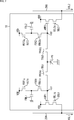
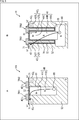
- FIG. 3 is a diagram illustrating an equivalent circuit of a pixel. It is a top view of a pixel. It is sectional drawing of a pixel.
- FIG. 14 is a diagram illustrating an effect of a pixel to which the present technology is applied.
- FIG. 14 is a diagram illustrating an effect of a pixel to which the present technology is applied.
- FIG. 14 is a diagram illustrating an effect of a pixel to which the present technology is applied.
- FIG. 4 is a plan view illustrating a planar shape of a vertical gate electrode unit. It is a figure showing the example of a pixel arrangement of a pixel array part.
- FIG. 4 is a plan view illustrating a planar shape of a vertical gate electrode unit. It is a figure showing the example of a pixel arrangement of a pixel array part.
- FIG. 4 is a diagram illustrating driving of a transfer transistor.
- FIG. 4 is a diagram illustrating driving of a transfer transistor.
- FIG. 3 is a plan view showing an example of the arrangement of a multilayer wiring layer. It is a top view showing a modification of a pixel. It is sectional drawing which shows the modification of a pixel. It is a top view of the pixel of 4 taps. It is a figure explaining drive of a pixel of 4 taps. It is a figure explaining application to a light receiving element of an electric field control type. It is a block diagram showing a configuration example of a distance measuring module to which the present technology is applied.
- FIG. 21 is a block diagram illustrating a configuration example of a smartphone as an electronic device to which the present technology is applied.
- FIG. 3 is a block diagram illustrating an example of a functional configuration of a camera head and a CCU.
- FIG. 1 is a block diagram illustrating an example of a schematic configuration of a vehicle control system. It is explanatory drawing which shows an example of the installation position of a vehicle exterior information detection part and an imaging part.
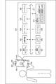
- FIG. 1 is a block diagram illustrating a schematic configuration example of a light receiving element to which the present technology is applied.
- the light receiving element 1 shown in FIG. 1 is an element that outputs distance measurement information by the indirect ToF method.
- the light receiving element 1 receives light (reflected light) reflected from an object with light (irradiation light) emitted from a predetermined light source, and outputs a depth image in which information on a distance to the object is stored as a depth value.
- the irradiation light emitted from the light source is, for example, infrared light having a wavelength in the range of 780 nm to 1000 nm, and is pulse light that is repeatedly turned on and off at a predetermined cycle.
- the light receiving element 1 has a pixel array unit 21 formed on a semiconductor substrate (not shown) and a peripheral circuit unit integrated on the same semiconductor substrate as the pixel array unit 21.
- the peripheral circuit unit includes, for example, a vertical drive unit 22, a column processing unit 23, a horizontal drive unit 24, a system control unit 25, and the like.
- the light receiving element 1 is further provided with a signal processing unit 26 and a data storage unit 27.
- the signal processing unit 26 and the data storage unit 27 may be mounted on the same substrate as the light receiving element 1 or may be arranged on a substrate in an imaging device different from the light receiving element 1.
- the pixel array section 21 has a configuration in which the pixels 10 that generate electric charges according to the amount of received light and output signals according to the electric charges are two-dimensionally arranged in rows and columns in a matrix. That is, the pixel array unit 21 has a plurality of pixels 10 that photoelectrically convert incident light and output a signal corresponding to the resulting charge. Details of the pixel 10 will be described later with reference to FIG.
- the row direction refers to the arrangement direction of the pixels 10 in the horizontal direction
- the column direction refers to the arrangement direction of the pixels 10 in the vertical direction.
- the row direction is the horizontal direction in the figure
- the column direction is the vertical direction in the figure.
- a pixel drive line 28 is wired along a row direction for each pixel row in a matrix pixel array, and two vertical signal lines 29 are provided in each pixel column along the column direction. Wired.
- the pixel drive line 28 transmits a drive signal for driving when reading a signal from the pixel 10.
- the pixel drive line 28 is shown as one line, but is not limited to one line.
- One end of the pixel drive line 28 is connected to an output end of the vertical drive unit 22 corresponding to each row.
- the vertical drive unit 22 includes a shift register, an address decoder, and the like, and drives each pixel 10 of the pixel array unit 21 simultaneously for all pixels or in units of rows. That is, the vertical drive unit 22 constitutes a drive unit that controls the operation of each pixel 10 of the pixel array unit 21 together with the system control unit 25 that controls the vertical drive unit 22.
- the detection signal output from each pixel 10 in the pixel row according to the drive control by the vertical drive unit 22 is input to the column processing unit 23 through the vertical signal line 29.
- the column processing unit 23 performs predetermined signal processing on the detection signal output from each pixel 10 through the vertical signal line 29, and temporarily holds the detection signal after the signal processing. Specifically, the column processing unit 23 performs noise removal processing, AD (Analog to digital) conversion processing, and the like as signal processing.
- the horizontal drive unit 24 is configured by a shift register, an address decoder, and the like, and sequentially selects unit circuits corresponding to the pixel columns of the column processing unit 23. By the selective scanning by the horizontal drive unit 24, the detection signals subjected to signal processing for each unit circuit in the column processing unit 23 are sequentially output.
- the system control unit 25 is configured by a timing generator or the like that generates various timing signals, and based on the various timing signals generated by the timing generator, a vertical driving unit 22, a column processing unit 23, and a horizontal driving unit 24. And the like.
- the signal processing unit 26 has at least an arithmetic processing function, and performs various signal processing such as arithmetic processing based on the detection signal output from the column processing unit 23.
- the data storage unit 27 temporarily stores data required for the signal processing in the signal processing unit 26.
- the light receiving element 1 configured as described above outputs a depth image in which distance information to an object is stored as a depth value in a pixel value.
- the light receiving element 1 is mounted on a vehicle, for example, an in-vehicle system that measures a distance to an object outside the vehicle, or measures a distance to an object such as a user's hand, and based on the measurement result, Can be mounted on a gesture recognition device or the like that recognizes the above gesture.
- FIG. 2 shows an equivalent circuit of the pixels 10 two-dimensionally arranged in the pixel array unit 21.
- the pixel 10 includes a photodiode PD as a photoelectric conversion element.
- the pixel 10 includes two transfer transistors TRG, two floating diffusion regions FD, additional capacitance FDL, two switching transistors FDG, one reset transistor RST, two amplification transistors AMP, and two selection transistors SEL.
- the transfer transistor TRG, the switching transistor FDG, the reset transistor RST, the amplification transistor AMP, and the selection transistor SEL are configured by, for example, N-type MOS transistors.
- the floating diffusion regions FD1 and FD2 are charge holding units for temporarily holding the charges transferred from the photodiode PD.
- the switching transistor FDG1 is turned on in response to the FD drive signal FDG1g supplied to the gate electrode being activated, thereby connecting the additional capacitance FDL1 to the floating diffusion region FD1.
- the switching transistor FDG2 is turned on in response to the FD drive signal FDG2g supplied to the gate electrode being activated, thereby connecting the additional capacitance FDL2 to the floating diffusion region FD2.
- the vertical drive unit 22 activates the switching transistors FDG1 and FDG2 to connect the floating diffusion region FD1 and the additional capacitance FDL1, and connects the floating diffusion region FD2 and the additional capacitance FDL2. Connect. Thereby, more charges can be accumulated at the time of high illuminance.
- the vertical drive unit 22 deactivates the switching transistors FDG1 and FDG2 to separate the additional capacitors FDL1 and FDL2 from the floating diffusion regions FD1 and FD2, respectively. Thereby, conversion efficiency can be improved.
- the reset transistor RST1 resets the potential of the floating diffusion region FD1 to a predetermined level (power supply voltage VDD) by being turned on in response to the reset drive signal RST1g supplied to the gate electrode being activated, in response to the active state.
- the reset transistor RST2 resets the potential of the floating diffusion region FD2 to a predetermined level (power supply voltage VDD) by being turned on in response to the reset drive signal RST2g supplied to the gate electrode being activated, in response to this. .
- the switching transistors FDG1 and FDG2 are also activated at the same time.
- the source electrode of the amplification transistor AMP1 is connected to the vertical signal line 29A via the selection transistor SEL1, thereby connecting to a constant current source (not shown) to form a source follower circuit.
- the source electrode of the amplification transistor AMP2 is connected to the vertical signal line 29B via the selection transistor SEL2, thereby connecting to a constant current source (not shown) to form a source follower circuit.
- the selection transistor SEL1 is connected between the source electrode of the amplification transistor AMP1 and the vertical signal line 29A.
- the selection transistor SEL1 becomes conductive in response to the selection signal SEL1g supplied to the gate electrode being activated, and outputs the detection signal VSL1 output from the amplification transistor AMP1 to the vertical signal line 29A.
- the selection transistor SEL2 is connected between the source electrode of the amplification transistor AMP2 and the vertical signal line 29B.
- the selection transistor SEL2 becomes conductive in response to the selection signal SEL2g supplied to the gate electrode being activated, and outputs the detection signal VSL2 output from the amplification transistor AMP2 to the vertical signal line 29B.
- the vertical drive unit 22 controls the transfer transistors TRG1 and TRG2, the switching transistors FDG1 and FDG2, the reset transistors RST1 and RST2, the amplification transistors AMP1 and AMP2, and the selection transistors SEL1 and SEL2 of the pixel 10.
- the additional capacitances FDL1 and FDL2 and the switching transistors FDG1 and FDG2 for controlling the connection may be omitted.
- the additional capacitance FDL is provided, and is selectively used in accordance with the amount of incident light. A range can be secured.
- a reset operation for resetting the charge of the pixel 10 is performed in all the pixels. That is, the reset transistors RST1 and RST1, the switching transistors FDG1 and FDG2, and the transfer transistors TRG1 and TRG2 are turned on, and the charges accumulated in the photodiode PD, the floating diffusion regions FD1 and FD2, and the additional capacitances FDL1 and FDL2 become constant voltage. Drained to source VDD and reset.
- the transfer transistors TRG1 and TRG2 are alternately driven. That is, in the first period, the transfer transistor TRG1 is controlled to be on and the transfer transistor TRG2 is controlled to be off. In the first period, the charge generated in the photodiode PD is transferred to the floating diffusion region FD1. In the second period following the first period, the transfer transistor TRG1 is controlled to be off, and the transfer transistor TRG2 is controlled to be on. In the second period, the charge generated in the photodiode PD is transferred to the floating diffusion region FD2. As a result, the charge generated in the photodiode PD is distributed to the floating diffusion regions FD1 and FD2 and accumulated.
- each pixel 10 of the pixel array unit 21 is selected line-sequentially.
- the selection transistors SEL1 and SEL2 are turned on.
- the charges accumulated in the floating diffusion region FD1 are output to the column processing unit 23 via the vertical signal line 29A as the detection signal VSL1.
- the charges accumulated in the floating diffusion region FD2 are output to the column processing unit 23 via the vertical signal line 29B as the detection signal VSL2.
- the reflected light received by the pixel 10 is delayed according to the distance to the object from the timing of irradiation by the light source.
- the distribution ratio of the electric charges stored in the two diffusion regions FD1 and FD2 changes according to the delay time according to the distance to the target object. The distance to can be obtained.
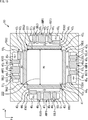
- FIG. 3 is a plan view of the pixel 10 showing the arrangement of the pixel circuits shown in FIG.
- the X direction in FIG. 3 corresponds to the row direction (horizontal direction) in FIG. 1, and the Y direction corresponds to the column direction (vertical direction) in FIG.
- a photodiode PD is formed in the central region of the rectangular pixel 10 in the N-type semiconductor region 41, and faces the photodiode PD in the X direction.
- TRG2 is arranged.
- the floating diffusion region FD1, the switching transistor FDG1, the additional capacitance FDL1, the reset transistor RST1, the amplification transistor AMP1, and the selection transistor SEL1 are arranged mirror-symmetrically.
- the transfer transistor TRG1 is constituted by a gate electrode 42 1, an N-type semiconductor region 41 as the source region, the N-type semiconductor region 43 1 serving as a drain region.
- N-type semiconductor region 41 as the source region is also used as the photodiode PD, N-type semiconductor region 43 1 serving as the drain region is shared with the floating diffusion region FD1.
- Switching transistor FDG1 is constituted by a gate electrode 44 1, an N-type semiconductor region 43 1 serving as a source region, an N-type semiconductor region 45 1 serving as a drain region.
- N-type semiconductor region 43 1 serving as the source region is also used as the floating diffusion region FD1,
- N-type semiconductor region 45 1 serving as the drain region is shared with additional capacitance FDL1.
- Reset transistor RST1 is constituted by a gate electrode 46 1, an N-type semiconductor region 45 1 serving as a source region, an N-type semiconductor region 47 1 serving as a drain region.
- Amplifying transistor AMP1 is constituted by a gate electrode 48 1, an N-type semiconductor region 47 1 serving as a drain region, an N-type semiconductor region 49 1 serving as a source region. N-type semiconductor region 47 1 serving as the drain region is shared with the drain region of the reset transistor RST1.
- Selection transistors SEL1 is constituted by a gate electrode 50 1, an N-type semiconductor region 49 1 serving as a drain region, an N-type semiconductor region 51 1 serving as a source region.
- the N-type semiconductor region 49 1 as a drain region is also used as a source region of the amplification transistor AMP1.
- the reset transistor RST1, the amplification transistor AMP1, and the selection transistor SEL1 are arranged in this order in the Y direction, and the transfer transistor TRG1 and the switching transistor FDG1 are arranged in the X direction.
- Transfer transistor TRG1, switching transistor FDG1, reset transistor RST1, amplifying transistor AMP1, and select transistor SEL1 are merely mirror-symmetrical in the X direction, and description thereof is omitted. Note that, when it is not necessary to particularly distinguish the gate electrodes, the drain regions, and the source regions of the transfer transistors TRG1 and TRG2, the transfer transistor TRG will be described with suffixes omitted.
- ⁇ P-type semiconductor region 52 is formed outside the N-type semiconductor region forming the drain region and the source region of each pixel transistor in pixel 10.
- the photodiode PD and the floating diffusion regions FD1 and FD2 are formed as rectangular regions longer in the Y direction than in the X direction.
- the gate electrode 42 1 and 42 2 of the transfer transistors TRG1 and TRG2, in the Y direction is the longitudinal direction, it is formed longer than the photodiode PD and the floating diffusion region FD1 and FD2.
- the gate width 61 of the gate electrode 42 1 and 42 2 of the transfer transistors TRG1 and TRG2 is greater than Y direction area width of the photodiode PD and the floating diffusion region FD1 and FD2.
- the distance 62 between the gate electrodes 42 1 and 42 2 of the transfer transistors TRG1 and TRG2 is shorter than the gate width 61 of the gate electrode 42 1 and 42 2 of the transfer transistors TRG1 and TRG2.
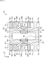
- FIG. 4 shows a cross-sectional view of the pixel 10.
- FIG. 4A is a cross-sectional view of the pixel 10 along the line a1-a2 in FIG. 3
- FIG. 4B is a cross-sectional view of the pixel 10 along the line b1-b2 in FIG.
- the vertical direction indicated by the Z axis in FIG. 4 corresponds to the depth direction of the substrate.
- the transfer transistors TRG1 and TRG2 are configured by vertical transistors having a gate electrode 42 extending in the substrate depth direction. More specifically, the gate electrode 42 1 of the transfer transistor TRG1 has a planar gate electrode portion 42T 1 formed on the upper surface of the semiconductor substrate 70 formed by P-type semiconductor region 52, the vertical gate electrode extending in the substrate depth direction It is composed of a section 42V 1.
- the gate electrode 42 2 of the transfer transistor TRG2 also a planar gate electrode portion 42T 2 formed on the upper surface of the semiconductor substrate 70 formed by P-type semiconductor region 52, and the vertical gate electrode portion 42V 2 extending in the substrate depth direction It is composed of
- the upper surface of the semiconductor substrate 70 on which the transfer transistors TRG1 and TRG2 are formed is the front surface side of the semiconductor substrate 70, and the gate insulating film 71 is formed at the substrate interface. Further, a multilayer wiring layer described later with reference to FIG. 12 is formed on the front side of the semiconductor substrate 70.
- a gate insulating film 71 and a P-type semiconductor region 72 are formed between the P-type semiconductor region 52 and the vertical gate electrode portion 42V.
- the impurity concentration of the P-type semiconductor region 72 is higher than the impurity concentration of the P-type semiconductor region 52, and the P-type semiconductor region 72 functions as a pinning region for suppressing generation of dark current.
- the lower surface side of the semiconductor substrate 70 which is the lower side in FIG. 4B, is an incident surface on which reflected light is incident, on which an unillustrated on-chip lens or the like is formed.
- the N-type semiconductor region 41 constituting the photodiode PD includes an N-type semiconductor region 41A below (on the back side of the semiconductor substrate) the vertical gate electrode portion 42V of the transfer transistor TRG and a vertical gate electrode portion 42 of the two transfer transistors TRG. It comprises an N-type semiconductor region 41B and an N-type semiconductor region 41C formed between them.
- the impurity concentrations of the N-type semiconductor regions 41A to 41C are increased in the order of the N-type semiconductor region 41A, the N-type semiconductor region 41B, and the N-type semiconductor region 41C.
- the impurity concentration of the N-type semiconductor region is described as “N ++”, “N +”, “N”, “N ⁇ ”, and the impurity concentration of “N ++” is the highest, “N ++”, It indicates that the impurity concentration decreases in the order of “N +”, “N”, and “N ⁇ ”.
- the vertical transfer transistor TRG can be formed by forming a trench (vertical hole) by dry etching from the substrate surface side, forming the gate insulating film 71, and then embedding polysilicon or the like serving as a gate electrode.
- the N-type semiconductor regions 43 1 and 43 2 as floating diffusion regions FD1 and FD2 Is formed.
- a plurality of vertical gate electrode portions 42V are formed at predetermined intervals so as to have a comb shape in a cross-sectional view in the Y direction which is the direction of the gate width 61.
- a gate insulating film 71 and a P-type semiconductor region 72 are formed on the outer peripheral portion of the plurality of vertical gate electrode portions 42V of the transfer transistor TRG, and the P-type semiconductor region 72 formed on the outer peripheral portion of the vertical gate electrode portion 42V is formed. Between them, the P-type semiconductor region 52 is formed with a lower concentration than the P-type semiconductor region 72.
- the two transfer transistors TRG1 and TRG2 of the pixel 10 are composed of vertical transistors having a plurality of vertical gate electrodes 42V in the gate width direction.
- a of FIG. 5 is a cross-sectional view taken along line b1-b2 of the pixel 10X when the transfer transistors TRG1 and TRG2 are formed of normal planar transistors.
- 5B is a cross-sectional view of the pixel 10 taken along line b1-b2, similar to FIG.
- portions corresponding to the pixel 10 are denoted by the same reference numerals as those of the pixel 10 for easy comparison.
- the state transfer transistor TRG1 is controlled to be on, electrons (charge) 80 generated by the N-type semiconductor region 41 constituting the photodiode PD, which is transferred to the N-type semiconductor region 43 1 serving as the floating diffusion region FD think of.
- the electrons 80 generated in the N-type semiconductor region 41 is transferred to the N-type semiconductor region 43 1.
- the N-type semiconductor region 41 of the pixel 10 is composed of only the N-type semiconductor regions 41B and 41C, and the N-type semiconductor region 41A closest to the rear surface of the substrate is not formed. Further, in order to transfer the electrons 80 generated at a deep position in the substrate, it is necessary to make the depth 81 of the N-type semiconductor region 41C having a high impurity concentration deeper than the depth 81 of the pixel 10 in FIG. is there.
- the transfer transistors TRG1 and TRG2 are generated in the N-type semiconductor region 41.
- electronic 80 in addition to the lower planar gate electrode portion 42T 1, through a channel formed between the comb-like plurality of vertical gate electrode portion 42V, is transferred to the N-type semiconductor region 43 1.
- electrons 80 as shown by the arrows in B of FIG. 5, can be moved linearly with respect to N-type semiconductor regions 43 1, it is possible to shorten the transfer path. As a result, the time required for the transfer is reduced.
- the plurality of vertical gate electrode portions 42V even the electrons 80 generated at a deep position in the substrate can be transferred at a high speed.
- the region 81A can be formed, and the depth 81 of the N-type semiconductor region 41C having a high impurity concentration can be made smaller than the depth 81 of the pixel 10X of FIG.
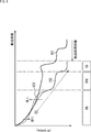
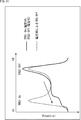
- FIG. 6 is a graph showing potentials and transfer paths when the planar transistor of FIG. 5A is used as the transfer transistor and when the vertical transistor of FIG. 5B is used as the transfer transistor.
- the vertical axis of the graph in FIG. 6 represents the potential, and the horizontal axis represents the electron transfer path from the photodiode PD to the floating diffusion region FD.
- a solid line 101 in the graph of FIG. 6 indicates a potential gradient in the pixel 10X using the planar transistor of FIG. 5A.
- the broken line 102 in the graph of FIG. 6 indicates a potential gradient when the transfer transistor of the pixel 10X in FIG. 5A is changed from a planar transistor to the same vertical transistor as the transfer transistor TRG.
- the N-type semiconductor region 41 as the photodiode PD is the same as the pixel 10X in FIG.
- the solid line 103 in the graph of FIG. 6 indicates the potential gradient of the pixel 10 in FIG. 5B. That is, the solid line 103 changes the transfer transistor of the pixel 10X in FIG. 5A from a planar transistor to a vertical transistor, and changes the N-type semiconductor region 41 as the photodiode PD as shown in FIG.
- the potential gradient when the depth 81 of the N-type semiconductor region 41C having a high impurity concentration is made shallow and the N-type semiconductor region 41A is formed near the rear surface of the substrate is shown.
- the transfer path can be shortened. Further, the depth 81 of the N-type semiconductor region 41C having a high impurity concentration is made shallow, and the N-type semiconductor region 41A is formed near the rear surface of the substrate, so that the potential of the deep portion of the photodiode PD is deepened. The potential can be reduced.
- the photoelectric conversion region can be enlarged and the saturation charge can be increased.
- FIG. 7 shows a potential distribution corresponding to the solid line 101, the dashed line 102, and the solid line 103 in FIG.
- FIG. 7 shows a cross-sectional view along line b1-b2 (upper part) and a potential distribution (lower part) of pixel 10X using a planar transistor as a transfer transistor.
- a in FIG. 7 corresponds to the solid line 101 in FIG.
- ⁇ Circle around (b) ⁇ of FIG. 7 shows a cross-sectional view along line b1-b2 (upper row) and a potential distribution (lower row) of pixel 10X using a vertical transistor as a transfer transistor. 7B corresponds to the broken line 102 in FIG.
- ⁇ Circle around (c) ⁇ in FIG. 7 shows a cross-sectional view of the pixel 10 of the light receiving element 1 along the line b1-b2 (upper part) and a potential distribution (lower part).
- C in FIG. 7 corresponds to the solid line 103 in FIG.
- each of the potential distributions A to C in FIG. 7 indicates a potential distribution in a state where the transfer transistor TRG1 is controlled to be turned on. Also, in the pixels 10X of FIGS. 7A and 7B, portions corresponding to the pixels 10 are denoted by the same reference numerals as those of the pixels 10, as in FIG.
- the N-type semiconductor region 41A is formed in a region near the rear surface of the substrate, so that the pixel 10 of FIGS.
- the depletion layer is enlarged to the vicinity of the back surface of the substrate. High sensitivity can be realized by this potential structure.
- FIG. 8 is a plan view illustrating the planar shape of the vertical gate electrode portion 42V.
- the planar shape of the vertical gate electrode portion 42V can be, for example, a round shape as shown in FIG. However, when the plane shape of the vertical gate electrode portion 42V is round, the area of the vertical gate electrode portion 42V with respect to the XY plane becomes large, and electrons may collide with the vertical gate electrode portion 42V, thereby lowering the transfer speed. There is.
- planar shape of the vertical gate electrode portion 42V is, for example, as shown in FIG. ) Can be formed in an elongated shape having a long width. Further, the planar shape of the vertical gate electrode portion 42V can be formed in an elongated shape in which the photodiode PD side is convex. This makes it difficult for electrons to collide with the vertical gate electrode portion 42V, thereby suppressing a decrease in transfer speed.
- FIG. 9 shows an example of a pixel array of the pixel array unit 21.
- FIG. 9 shows only 16 ⁇ 4 ⁇ 16 pixels in which four pixels 10 are arranged in the row and column directions due to space limitations, but the number of pixels is not limited to this.
- reference numerals are omitted due to space limitations.
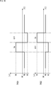
- FIG. 10 is a diagram showing an applied voltage when driving the transfer transistor TRG.
- the pixel 10 of the light receiving element 1 distributes electric charges to the floating diffusion regions FD1 and FD2 by alternately performing control of turning on one of the two transfer transistors TRG1 and TRG2 and turning off the other.
- the vertical drive unit 22 sets the applied voltage of one of the transfer transistors TRG (for example, the transfer transistor TRG1) to be turned on to the pixel 10 as a first predetermined drive, a positive predetermined voltage VA, and the other of the transfer transistors to be turned off. Control can be performed such that the voltage applied to the TRG (for example, the transfer transistor TRG2) is set to a predetermined negative voltage VB (first negative bias VB).
- the first negative bias VB is a negative bias for pinning for suppressing a white point and a dark current.
- the vertical drive unit 22 applies a voltage applied to one of the transfer transistors TRG (for example, the transfer transistor TRG1) to be turned on to the pixel 10 as a second drive, as shown in FIG.
- the control can be performed such that the voltage applied to the other transfer transistor TRG (for example, the transfer transistor TRG2) to be turned off is set to the voltage VA and the negative predetermined voltage VC (second negative bias VC).
- the second negative bias VC is a larger negative bias than the first negative bias VB for pinning.
- FIG. 11 shows the potential between the two transfer transistors TRG1 and TRG2 when the second drive is performed.
- the solid line in the graph of FIG. 11 indicates the potential between the two transfer transistors TRG1 and TRG2 when the second drive is performed, and the broken line indicates the potential when the transfer transistors TRG1 and TRG2 are turned off by the first negative bias VB. The potential is shown.
- the gradient of the electric field can be further improved.
- the size can be increased, and charge transfer can be assisted. Therefore, the charge transfer characteristics can be improved by the second driving.
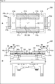
- FIG. 12 shows an arrangement example of a multilayer wiring layer of the light receiving element 1 formed on the front surface side of the semiconductor substrate 70.
- FIG. 12 portions corresponding to those in FIG. 3 are denoted by the same reference numerals, but some reference numerals are omitted.
- the light receiving element 1 has, for example, a multilayer wiring layer including four wiring layers including a first wiring layer M1 to a fourth wiring layer M4 and an interlayer insulating layer.
- the four wiring layers are, in order from the side closer to the semiconductor substrate 70, a first wiring layer M1, a second wiring layer M2, a third wiring layer M3, and a fourth wiring layer M4.
- FIG. 12A shows the gate electrode and the N-type semiconductor region of the pixel transistor formed on the surface side of the semiconductor substrate 70, the first wiring layer M1, and the contact between the gate electrode of the pixel transistor and the first wiring layer M1. It is a top view showing arrangement.
- the first wiring layer M1 is formed at least at the boundary between the pixels 10, and is connected to GND.
- the first wiring layer M1 is connected to the gate electrode of the pixel transistor via a contact.
- N-type semiconductor region 43 1 serving as the floating diffusion region FD1 via the wiring 151 1 is connected to the gate electrode 48 1 of the amplification transistor AMP1
- N-type semiconductor region 43 2 that functions as a floating diffusion region FD2 is wiring 151 2 through, and is connected to the gate electrode 48 and second amplifying transistor AMP2.
- ⁇ B of FIG. 12 is a plan view showing the arrangement of the first wiring layer M1, the second wiring layer M2, and the vias connecting the first wiring layer M1 and the second wiring layer M2.
- 12C is a plan view showing the arrangement of the second wiring layer M2, the third wiring layer M3, and vias connecting the second wiring layer M2 and the third wiring layer M3.
- control lines and power lines for transmitting the pixel array section 21 in the horizontal direction are arranged.
- the third wiring layer M3 includes wirings 161 1 and 161 2 for transmitting transfer drive signals TRG1g and TRG2g supplied to the gate electrodes of the transfer transistors TRG1 and TRG2, and gate electrodes of the switching transistors FDG1 and FDG2.
- 12D is a plan view showing the arrangement of the third wiring layer M3, the fourth wiring layer M4, and vias connecting the third wiring layer M3 and the fourth wiring layer M4.
- the vertical signal lines 29A and 29B for transmitting the pixel array section 21 in the vertical direction and the power supply lines are arranged.
- FIG. 13 and FIG. 14 are diagrams illustrating modified examples of the pixel 10.
- FIG. 13 is a plan view of a modification of the pixel 10
- FIG. 14 is a cross-sectional view of a modification of the pixel 10.
- the plan view of FIG. 13 corresponds to the plan view of the pixel 10 shown in FIG. 3
- the cross-sectional view of FIG. 14 corresponds to the cross-sectional view of the pixel 10 shown in FIG.
- FIGS. 13 and 14 show a pixel structure when the capacitance of the floating diffusion regions FD1 and FD2 is reduced in order to increase the conversion efficiency.
- the circuit configuration of the pixel 10 is the same as the equivalent circuit shown in FIG.
- N-type area of the semiconductor regions 43 1 and 43 2 as floating diffusion regions FD1 and FD2 (volume) is formed smaller as compared with FIG. Transfer transistors TRG1 and the gate electrode 42 1 of TRG2 and 42 2 of the gate width 201, shorter than the gate width 61 of the pixel 10 of Figure 3.
- the transfer transistor TRG As the N-type semiconductor regions 43 1 and 43 change 2 region size as the floating diffusion region FD1 and FD2, the transfer transistor TRG, switching transistors FDG, a reset transistor RST, the amplifying transistor AMP, and the pixel transistors of the selection transistor SEL The placement has been changed.
- the N-type semiconductor region 51 1 serving as the source region of the select transistor SEL1 and SEL2, and is formed in a region of the pixel 10 adjacent to the vertical direction.
- N-type semiconductor region 43 1 serving as the floating diffusion region FD1 via the wiring 151 is connected to the gate electrode 48 1 of the amplification transistor AMP1
- N-type semiconductor region 43 which serves as a floating diffusion region FD2 2 through the wiring 151 2 is connected to the gate electrode 48 and second amplifying transistor AMP2.
- FIG. 14A is a cross-sectional view of the pixel 10 along the line a1-a2 in FIG. 13, and FIG. 14B is a cross-sectional view of the pixel 10 along the line b1-b2 in FIG.
- the gate electrode 42 2 of the transfer transistor TRG2 includes a planar gate electrode portion 42T 2, is constituted by one and the vertical gate electrode portion 42V 2.
- the number of the vertical gate electrode portions 42V may be plural, such as two or three, depending on the gate width 201 of the gate electrode 42 of the transfer transistor TRG.
- FIG. 15 is a plan view showing still another modified example of the pixel 10.
- the pixel 10 shown in FIGS. 3 and 13 has two transfer transistors TRG1 and TRG2 and floating diffusion regions FD1 and FD2 with respect to one photodiode PD, and stores the charges generated by the photodiode PD. It has a two-tap pixel structure that is divided into two floating diffusion regions FD1 and FD2.
- the pixel 10 shown in FIG. 15 has four transfer transistors TRG1 to TRG4 and floating diffusion regions FD1 to FD4 for one photodiode PD, and is generated by the photodiode PD. It has a four-tap pixel structure for distributing charges to four floating diffusion regions FD1 to FD4.
- the pixel 10 has four transfer transistors TRG, floating diffusion regions FD, additional capacitances FDL, switching transistors FDG, reset transistors RST, amplification transistors AMP, and four selection transistors SEL.
- a combination (one set) of the transfer transistor TRG, the floating diffusion region FD, the additional capacitance FDL, the switching transistor FDG, the reset transistor RST, the amplification transistor AMP, and the selection transistor SEL is a rectangular pixel region.
- the four taps in FIG. 15 are arranged on each side.
- each set of the transfer transistor TRG, the floating diffusion region FD, the additional capacitance FDL, the switching transistor FDG, the reset transistor RST, the amplification transistor AMP, and the selection transistor SEL has any one of 1 to 4. They are distinguished by letters.
- the cross-sectional view of the pixel 10 along the line a1-a2 in FIG. 15 is the same as that in FIG. 4A, and all the transfer transistors TRG are configured by vertical transistors. Note that, of course, the number of the vertical gate electrode portions 42V of the transfer transistor TRG may be different from the case of two taps.
- the distance 222 between the gate electrodes 42 of the two transfer transistors TRG opposed to each other is set to the same length as the gate width 221 of the gate electrode 42 of the transfer transistor TRG.
- the transfer transistor TRG is a vertical transistor, the modulation capability is enhanced, and a second negative bias VC larger than the first negative bias VB for pinning is applied to the transfer transistor TRG on the side to be turned off. By performing the second drive, high-speed transfer of charges is possible.
- FIG. 16 is a timing chart illustrating the second drive in the 4-tap pixel 10.
- the vertical drive unit 22 sets the transfer transistor TRG opposite to the predetermined one transfer transistor TRG to be turned on to the second negative bias VC, and sets the remaining two transfer transistors orthogonal to each other.
- One transfer transistor TRG is controlled to the first negative bias VB.
- the vertical driving unit 22 turns on the transfer transistor TRG1, controls the transfer transistor TRG3 to the second negative bias VC, and sets the transfer transistors TRG2 and TRG4 to the first negative bias. Control to VB.
- the vertical drive unit 22 turns on the transfer transistor TRG2, controls the transfer transistor TRG4 to the second negative bias VC, and sets the transfer transistors TRG1 and TRG3 to the first negative bias VB. To control.
- the vertical drive unit 22 turns on the transfer transistor TRG3, controls the transfer transistor TRG1 to the second negative bias VC, and sets the transfer transistors TRG2 and TRG4 to the first negative bias VB. To control.
- the vertical drive unit 22 turns on the transfer transistor TRG4, controls the transfer transistor TRG2 to the second negative bias VC, and sets the transfer transistors TRG1 and TRG3 to the first negative bias VB. To control.
- FIG. 17A is a plan view of a pixel of the electric field control type light receiving element
- FIG. 17B is a sectional view and a potential diagram of the pixel of the electric field control type light receiving element.
- the pixel 300 of the light-receiving element of the electric field control type transfers the electric charge generated in the N-type semiconductor region 301 as the photoelectric conversion region to a pair of the first electric field control electrodes 311a and 311b and a pair of the second electric field control electrodes 311a and 311b adjacent thereto.
- the electric charge is distributed to the two charge accumulation regions 313a and 313b.
- the charges stored in the two charge storage regions 313a and 313b are transferred to the charge readout regions 314a and 314b by the transfer transistors TRGa and TRGb, respectively.
- the N-type semiconductor region 301 which is a photoelectric conversion region, that has passed through the rectangular opening region of the light shielding plate 302 shown in FIG.
- a pair of first electric field control electrodes 311a and 311b and a pair of adjacent second electric field control electrodes 312a and 312b shown in FIG. 17A are arranged between the light shielding plate 302 and the insulating film 303.
- the P-type semiconductor region 304 between the N-type semiconductor region 301 and the insulating film 303 is a pinning layer.
- the configuration of the transfer transistors TRG1 and TRG2 described above that is, A configuration of a vertical transistor having a comb-shaped vertical gate electrode portion 42V can be employed.
- the modulation ability is improved and an electric field is easily generated, so that the transfer characteristics can be improved.
- FIG. 18 is a block diagram illustrating a configuration example of a ranging module that outputs ranging information using the light receiving element 1 described above.
- the distance measuring module 500 includes a light emitting unit 511, a light emission control unit 512, and a light receiving unit 513.
- the light emitting unit 511 has a light source that emits light of a predetermined wavelength, and emits irradiation light whose brightness varies periodically to irradiate the object.
- the light emitting unit 511 includes, as a light source, a light emitting diode that emits infrared light having a wavelength in the range of 780 nm to 1000 nm, and emits light in synchronization with a rectangular wave light emission control signal CLKp supplied from the light emission control unit 512. Generates light.
- the light emission control signal CLKp is not limited to a rectangular wave as long as it is a periodic signal.
- the light emission control signal CLKp may be a sine wave.
- the light emission control unit 512 supplies the light emission control signal CLKp to the light emitting unit 511 and the light receiving unit 513, and controls the irradiation timing of the irradiation light.
- the frequency of the light emission control signal CLKp is, for example, 20 megahertz (MHz).
- the frequency of the light emission control signal CLKp is not limited to 20 megahertz (MHz) but may be 5 megahertz (MHz).
- the light receiving unit 513 receives the light reflected from the object, calculates distance information for each pixel according to the light reception result, and generates a depth image in which the distance to the object is represented by a gradation value for each pixel. Output.
- the light receiving element 1 as the light receiving unit 513 alternately drives a plurality of transfer transistors TRG of each pixel 10 of the pixel array unit 21 based on, for example, a light emission control signal CLKp, and generates a plurality of electric charges generated by the photodiode PD.
- the light receiving element 1 calculates distance information for each pixel from the signal intensities detected by the plurality of charge storage units.
- the light receiving element 1 described above can be incorporated as the light receiving unit 513 of the distance measuring module 500 that obtains and outputs distance information to a subject by the indirect ToF method. Thereby, the ranging characteristics of the ranging module 500 can be improved.
- the light receiving element 1 can be applied to a distance measuring module as described above.
- various electronic devices such as an imaging device having a distance measuring function, such as a digital still camera and a digital video camera, and a smartphone having a distance measuring function. Can be applied to
- FIG. 19 is a block diagram illustrating a configuration example of a smartphone as an electronic device to which the present technology is applied.
- the smartphone 601 includes a distance measuring module 602, an imaging device 603, a display 604, a speaker 605, a microphone 606, a communication module 607, a sensor unit 608, a touch panel 609, and a control unit 610, which are connected to a bus 611. It is connected and configured through.
- the control unit 610 has functions as an application processing unit 621 and an operation system processing unit 622 when the CPU executes the program.
- the distance measuring module 500 shown in FIG. 18 is applied to the distance measuring module 602.
- the distance measurement module 602 is disposed in front of the smartphone 601 and performs distance measurement for a user of the smartphone 601 to obtain a depth value of a surface shape of the user's face, hand, finger, or the like. Can be output as
- the imaging device 603 is disposed on the front of the smartphone 601 and captures an image of the user of the smartphone 601 by performing imaging with the user of the smartphone 601 as a subject.
- a configuration in which the imaging device 603 is also arranged on the back surface of the smartphone 601 may be adopted.
- the display 604 displays an operation screen for performing processing by the application processing unit 621 and the operation system processing unit 622, an image captured by the imaging device 603, and the like.
- the speaker 605 and the microphone 606 output, for example, the voice of the other party and collect the voice of the user when making a call with the smartphone 601.
- the communication module 607 is a network via a communication network such as the Internet, a public telephone line network, a wide area communication network for wireless mobile such as a so-called 3G line or 4G line, a WAN (Wide Area Network), and a LAN (Local Area Network). It performs communication, short-range wireless communication such as Bluetooth (registered trademark) and NFC (Near Field Communication).
- the sensor unit 608 senses speed, acceleration, proximity, and the like, and the touch panel 609 acquires a user's touch operation on the operation screen displayed on the display 604.
- the application processing unit 621 performs a process for providing various services by the smartphone 601. For example, based on the depth value supplied from the distance measurement module 602, the application processing unit 621 can perform a process of creating a computer graphics face that virtually reproduces the user's expression and displaying the face on the display 604. . Further, the application processing unit 621 can perform, for example, a process of creating three-dimensional shape data of an arbitrary three-dimensional object based on the depth value supplied from the distance measurement module 602.
- the operation system processing unit 622 performs processing for realizing basic functions and operations of the smartphone 601. For example, the operation system processing unit 622 can perform a process of authenticating the user's face and unlocking the smartphone 601 based on the depth value supplied from the distance measurement module 602. Further, the operation system processing unit 622 performs, for example, a process of recognizing a user's gesture based on the depth value supplied from the distance measurement module 602, and performs a process of inputting various operations according to the gesture. Can be.
- the smartphone 601 configured as described above, by applying the above-described distance measurement module 500 as the distance measurement module 602, for example, the distance to a predetermined object is measured and displayed, or the tertiary of the predetermined object is measured. Processing for creating and displaying original shape data can be performed.
- Example of application to endoscopic surgery system The technology (the present technology) according to the present disclosure can be applied to various products.
- the technology according to the present disclosure may be applied to an endoscopic surgery system.
- FIG. 20 is a diagram illustrating an example of a schematic configuration of an endoscopic surgery system to which the technology (the present technology) according to the present disclosure may be applied.
- FIG. 20 shows a state in which an operator (doctor) 11131 is performing an operation on a patient 11132 on a patient bed 11133 using the endoscopic surgery system 11000.
- the endoscopic surgery system 11000 includes an endoscope 11100, other surgical tools 11110 such as an insufflation tube 11111 and an energy treatment tool 11112, and a support arm device 11120 that supports the endoscope 11100.
- a cart 11200 on which various devices for endoscopic surgery are mounted.
- the endoscope 11100 includes a lens barrel 11101 having a region of a predetermined length from the distal end inserted into the body cavity of the patient 11132, and a camera head 11102 connected to the proximal end of the lens barrel 11101.
- the endoscope 11100 which is configured as a so-called rigid endoscope having a hard barrel 11101 is illustrated.
- the endoscope 11100 may be configured as a so-called flexible endoscope having a soft barrel. Good.
- An opening in which the objective lens is fitted is provided at the tip of the lens barrel 11101.
- a light source device 11203 is connected to the endoscope 11100, and light generated by the light source device 11203 is guided to a distal end of the lens barrel by a light guide extending inside the lens barrel 11101, and an objective is provided. The light is radiated toward the observation target in the body cavity of the patient 11132 via the lens.
- the endoscope 11100 may be a direct view, a perspective view, or a side view.
- An optical system and an image sensor are provided inside the camera head 11102, and the reflected light (observation light) from the observation target is focused on the image sensor by the optical system.
- the observation light is photoelectrically converted by the imaging element, and an electric signal corresponding to the observation light, that is, an image signal corresponding to the observation image is generated.
- the image signal is transmitted to a camera control unit (CCU: ⁇ Camera ⁇ Control ⁇ Unit) 11201 as RAW data.
- the $ CCU 11201 is configured by a CPU (Central Processing Unit), a GPU (Graphics Processing Unit), and the like, and controls the operations of the endoscope 11100 and the display device 11202 overall. Further, the CCU 11201 receives an image signal from the camera head 11102, and performs various image processing on the image signal for displaying an image based on the image signal, such as a development process (demosaicing process).
- a development process demosaicing process
- the display device 11202 displays an image based on an image signal on which image processing has been performed by the CCU 11201 under the control of the CCU 11201.
- the light source device 11203 includes a light source such as an LED (Light Emitting Diode), for example, and supplies the endoscope 11100 with irradiation light when imaging an operation part or the like.
- a light source such as an LED (Light Emitting Diode), for example, and supplies the endoscope 11100 with irradiation light when imaging an operation part or the like.
- the input device 11204 is an input interface to the endoscopic surgery system 11000.
- the user can input various information and input instructions to the endoscopic surgery system 11000 via the input device 11204.
- the user inputs an instruction or the like to change imaging conditions (type of irradiation light, magnification, focal length, and the like) by the endoscope 11100.
- the treatment instrument control device 11205 controls the driving of the energy treatment instrument 11112 for cauterizing, incising a tissue, sealing a blood vessel, and the like.
- the insufflation device 11206 is used to inflate the body cavity of the patient 11132 for the purpose of securing the visual field by the endoscope 11100 and securing the working space of the operator.
- the recorder 11207 is a device that can record various types of information related to surgery.
- the printer 11208 is a device that can print various types of information on surgery in various formats such as text, images, and graphs.
- the light source device 11203 that supplies the endoscope 11100 with irradiation light at the time of imaging the operation site can be configured by a white light source configured by, for example, an LED, a laser light source, or a combination thereof.
- a white light source configured by a combination of the RGB laser light sources
- the output intensity and output timing of each color (each wavelength) can be controlled with high accuracy. It can be carried out.
- laser light from each of the RGB laser light sources is irradiated to the observation target in a time-division manner, and the driving of the image pickup device of the camera head 11102 is controlled in synchronization with the irradiation timing, so that each of the RGB laser light sources is controlled. It is also possible to capture the image obtained in a time-division manner. According to this method, a color image can be obtained without providing a color filter in the image sensor.
- the driving of the light source device 11203 may be controlled so as to change the intensity of the output light every predetermined time.
- the driving of the image pickup device of the camera head 11102 in synchronization with the timing of the change of the light intensity, an image is acquired in a time-division manner, and the image is synthesized, so that a high dynamic image without a so-called blackout or whiteout is obtained.
- An image of the range can be generated.
- the light source device 11203 may be configured to be able to supply light in a predetermined wavelength band corresponding to special light observation.
- special light observation for example, by utilizing the wavelength dependence of light absorption in body tissue, by irradiating light in a narrower band compared to irradiation light (ie, white light) during normal observation, the surface of the mucous membrane is exposed.
- a narrow band light observation (Narrow / Band / Imaging) for photographing a predetermined tissue such as a blood vessel with high contrast is performed.
- a fluorescence observation for obtaining an image by fluorescence generated by irradiating the excitation light may be performed.
- a body tissue is irradiated with excitation light to observe fluorescence from the body tissue (autofluorescence observation), or a reagent such as indocyanine green (ICG) is locally injected into the body tissue and the body tissue is subjected to the fluorescence observation.
- ICG indocyanine green
- Irradiation with excitation light corresponding to the fluorescence wavelength of the reagent can be performed to obtain a fluorescence image.
- the light source device 11203 can be configured to be able to supply narrowband light and / or excitation light corresponding to such special light observation.
- FIG. 21 is a block diagram showing an example of a functional configuration of the camera head 11102 and the CCU 11201 shown in FIG.
- the camera head 11102 includes a lens unit 11401, an imaging unit 11402, a driving unit 11403, a communication unit 11404, and a camera head control unit 11405.
- the CCU 11201 includes a communication unit 11411, an image processing unit 11412, and a control unit 11413.
- the camera head 11102 and the CCU 11201 are communicably connected to each other by a transmission cable 11400.
- the lens unit 11401 is an optical system provided at a connection with the lens barrel 11101. Observation light taken in from the tip of the lens barrel 11101 is guided to the camera head 11102, and enters the lens unit 11401.
- the lens unit 11401 is configured by combining a plurality of lenses including a zoom lens and a focus lens.
- the imaging unit 11402 includes an imaging element.
- the number of imaging elements constituting the imaging unit 11402 may be one (so-called single-panel type) or plural (so-called multi-panel type).
- image signals corresponding to RGB may be generated by the imaging elements, and a color image may be obtained by combining the image signals.
- the imaging unit 11402 may be configured to include a pair of imaging devices for acquiring right-eye and left-eye image signals corresponding to 3D (Dimensional) display. By performing the 3D display, the operator 11131 can more accurately grasp the depth of the living tissue in the operative part.
- a plurality of lens units 11401 may be provided for each imaging device.
- the imaging unit 11402 does not necessarily need to be provided in the camera head 11102.
- the imaging unit 11402 may be provided inside the lens barrel 11101 immediately after the objective lens.
- the driving unit 11403 is configured by an actuator, and moves the zoom lens and the focus lens of the lens unit 11401 by a predetermined distance along the optical axis under the control of the camera head control unit 11405.
- the magnification and the focus of the image captured by the imaging unit 11402 can be appropriately adjusted.
- the communication unit 11404 is configured by a communication device for transmitting and receiving various information to and from the CCU 11201.
- the communication unit 11404 transmits the image signal obtained from the imaging unit 11402 as RAW data to the CCU 11201 via the transmission cable 11400.
- the communication unit 11404 receives a control signal for controlling the driving of the camera head 11102 from the CCU 11201 and supplies the control signal to the camera head control unit 11405.
- the control signal includes, for example, information indicating the frame rate of the captured image, information indicating the exposure value at the time of imaging, and / or information indicating the magnification and focus of the captured image. Contains information about the condition.
- imaging conditions such as the frame rate, the exposure value, the magnification, and the focus may be appropriately designated by the user, or may be automatically set by the control unit 11413 of the CCU 11201 based on the acquired image signal. Good.
- a so-called AE (Auto Exposure) function, an AF (Auto Focus) function, and an AWB (Auto White Balance) function are mounted on the endoscope 11100.
- the camera head controller 11405 controls driving of the camera head 11102 based on a control signal from the CCU 11201 received via the communication unit 11404.
- the communication unit 11411 is configured by a communication device for transmitting and receiving various information to and from the camera head 11102.
- the communication unit 11411 receives an image signal transmitted from the camera head 11102 via the transmission cable 11400.
- the communication unit 11411 transmits a control signal for controlling driving of the camera head 11102 to the camera head 11102.
- the image signal and the control signal can be transmitted by electric communication, optical communication, or the like.
- the image processing unit 11412 performs various types of image processing on an image signal that is RAW data transmitted from the camera head 11102.
- the control unit 11413 performs various kinds of control relating to imaging of the operation section and the like by the endoscope 11100 and display of a captured image obtained by imaging the operation section and the like. For example, the control unit 11413 generates a control signal for controlling driving of the camera head 11102.
- control unit 11413 causes the display device 11202 to display a captured image showing the operative part or the like based on the image signal on which the image processing is performed by the image processing unit 11412.
- the control unit 11413 may recognize various objects in the captured image using various image recognition techniques. For example, the control unit 11413 detects a surgical tool such as forceps, a specific living body site, a bleeding, a mist at the time of using the energy treatment tool 11112, and the like by detecting the shape and color of the edge of the object included in the captured image. Can be recognized.
- the control unit 11413 may use the recognition result to superimpose and display various types of surgery support information on the image of the operative site. By superimposing the operation support information and presenting it to the operator 11131, the burden on the operator 11131 can be reduced, and the operator 11131 can surely proceed with the operation.
- the transmission cable 11400 connecting the camera head 11102 and the CCU 11201 is an electric signal cable corresponding to electric signal communication, an optical fiber corresponding to optical communication, or a composite cable thereof.
- the communication is performed by wire using the transmission cable 11400, but the communication between the camera head 11102 and the CCU 11201 may be performed wirelessly.
- the technology according to the present disclosure can be applied to the imaging unit 11402 in the configuration described above.
- the light receiving element 1 including the pixel 10 can be applied as a part of the configuration of the imaging unit 11402.
- the technology according to the present disclosure may be applied to, for example, a microscopic surgery system and the like.
- the technology (the present technology) according to the present disclosure can be applied to various products.
- the technology according to the present disclosure is realized as a device mounted on any type of moving object such as an automobile, an electric vehicle, a hybrid electric vehicle, a motorcycle, a bicycle, a personal mobility, an airplane, a drone, a ship, and a robot. May be.
- FIG. 22 is a block diagram illustrating a schematic configuration example of a vehicle control system that is an example of a mobile object control system to which the technology according to the present disclosure can be applied.
- Vehicle control system 12000 includes a plurality of electronic control units connected via communication network 12001.
- the vehicle control system 12000 includes a drive system control unit 12010, a body system control unit 12020, an outside information detection unit 12030, an inside information detection unit 12040, and an integrated control unit 12050.
- a microcomputer 12051, an audio / video output unit 12052, and a vehicle-mounted network I / F (interface) 12053 are illustrated.
- the drive system control unit 12010 controls the operation of the device related to the drive system of the vehicle according to various programs.
- the drive system control unit 12010 includes a drive force generation device for generating a drive force of the vehicle such as an internal combustion engine or a drive motor, a drive force transmission mechanism for transmitting the drive force to wheels, and a steering angle of the vehicle. It functions as a control device such as a steering mechanism for adjusting and a braking device for generating a braking force of the vehicle.
- the body control unit 12020 controls the operation of various devices mounted on the vehicle body according to various programs.
- the body control unit 12020 functions as a keyless entry system, a smart key system, a power window device, or a control device for various lamps such as a head lamp, a back lamp, a brake lamp, a blinker, a fog lamp, and the like.
- a radio wave or various switch signals transmitted from a portable device that substitutes for a key may be input to the body control unit 12020.
- the body control unit 12020 receives the input of these radio waves or signals, and controls a door lock device, a power window device, a lamp, and the like of the vehicle.
- Out-of-vehicle information detection unit 12030 detects information external to the vehicle on which vehicle control system 12000 is mounted.
- an imaging unit 12031 is connected to the outside-of-vehicle information detection unit 12030.
- the out-of-vehicle information detection unit 12030 causes the image capturing unit 12031 to capture an image outside the vehicle, and receives the captured image.
- the outside-of-vehicle information detection unit 12030 may perform an object detection process or a distance detection process of a person, a vehicle, an obstacle, a sign, a character on a road surface, or the like based on the received image.
- the imaging unit 12031 is an optical sensor that receives light and outputs an electric signal according to the amount of received light.
- the imaging unit 12031 can output the electric signal as an image or can output the electric signal as distance measurement information.
- the light received by the imaging unit 12031 may be visible light or non-visible light such as infrared light.
- the in-vehicle information detection unit 12040 detects information in the vehicle.
- the in-vehicle information detection unit 12040 is connected to, for example, a driver status detection unit 12041 that detects the status of the driver.
- the driver state detection unit 12041 includes, for example, a camera that captures an image of the driver, and the in-vehicle information detection unit 12040 determines the degree of fatigue or concentration of the driver based on the detection information input from the driver state detection unit 12041. The calculation may be performed, or it may be determined whether the driver has fallen asleep.
- the microcomputer 12051 calculates a control target value of the driving force generation device, the steering mechanism, or the braking device based on the information on the inside and outside of the vehicle acquired by the outside information detection unit 12030 or the inside information detection unit 12040, and the drive system control unit.
- a control command can be output to 12010.
- the microcomputer 12051 implements the functions of ADAS (Advanced Driver Assistance System) including vehicle collision avoidance or impact mitigation, following running based on the following distance, vehicle speed maintaining running, vehicle collision warning, vehicle lane departure warning, and the like.
- ADAS Advanced Driver Assistance System
- the cooperative control for the purpose can be performed.
- the microcomputer 12051 controls the driving force generation device, the steering mechanism, the braking device, and the like based on information on the surroundings of the vehicle acquired by the outside-of-vehicle information detection unit 12030 or the inside-of-vehicle information detection unit 12040, so that the driver It is possible to perform cooperative control for automatic driving or the like in which the vehicle travels autonomously without relying on the operation.
- the microcomputer 12051 can output a control command to the body system control unit 12020 based on information on the outside of the vehicle acquired by the outside information detection unit 12030.
- the microcomputer 12051 controls the headlamp in accordance with the position of the preceding vehicle or the oncoming vehicle detected by the outside-of-vehicle information detection unit 12030, and performs cooperative control for the purpose of anti-glare such as switching a high beam to a low beam. It can be carried out.
- the audio image output unit 12052 transmits at least one of an audio signal and an image signal to an output device capable of visually or audibly notifying a passenger of the vehicle or the outside of the vehicle of information.
- an audio speaker 12061, a display unit 12062, and an instrument panel 12063 are illustrated as output devices.
- the display unit 12062 may include, for example, at least one of an on-board display and a head-up display.
- FIG. 23 is a diagram illustrating an example of an installation position of the imaging unit 12031.
- the vehicle 12100 has imaging units 12101, 12102, 12103, 12104, and 12105 as the imaging unit 12031.
- the imaging units 12101, 12102, 12103, 12104, and 12105 are provided, for example, at positions such as a front nose, a side mirror, a rear bumper, a back door, and an upper portion of a windshield in the vehicle interior of the vehicle 12100.
- An imaging unit 12101 provided in the front nose and an imaging unit 12105 provided above a windshield in the vehicle cabin mainly acquire an image in front of the vehicle 12100.
- the imaging units 12102 and 12103 provided in the side mirror mainly acquire images of the side of the vehicle 12100.
- the imaging unit 12104 provided in the rear bumper or the back door mainly acquires an image behind the vehicle 12100.
- the forward images acquired by the imaging units 12101 and 12105 are mainly used for detecting a preceding vehicle, a pedestrian, an obstacle, a traffic light, a traffic sign, a lane, and the like.
- FIG. 23 shows an example of the imaging range of the imaging units 12101 to 12104.
- the imaging range 12111 indicates the imaging range of the imaging unit 12101 provided on the front nose
- the imaging ranges 12112 and 12113 indicate the imaging ranges of the imaging units 12102 and 12103 provided on the side mirrors, respectively
- the imaging range 12114 indicates 14 shows an imaging range of an imaging unit 12104 provided in a rear bumper or a back door. For example, by overlaying image data captured by the imaging units 12101 to 12104, a bird's-eye view image of the vehicle 12100 viewed from above can be obtained.
- At least one of the imaging units 12101 to 12104 may have a function of acquiring distance information.
- at least one of the imaging units 12101 to 12104 may be a stereo camera including a plurality of imaging elements or an imaging element having pixels for detecting a phase difference.
- the microcomputer 12051 calculates the distance to each three-dimensional object in the imaging ranges 12111 to 12114 and the temporal change of this distance (relative speed with respect to the vehicle 12100). , It is possible to extract, as a preceding vehicle, a three-dimensional object that travels at a predetermined speed (for example, 0 km / h or more) in a direction substantially the same as the vehicle 12100, which is the closest three-dimensional object on the traveling path of the vehicle 12100. it can.
- a predetermined speed for example, 0 km / h or more
- microcomputer 12051 can set an inter-vehicle distance to be secured before the preceding vehicle, and perform automatic brake control (including follow-up stop control), automatic acceleration control (including follow-up start control), and the like. As described above, it is possible to perform cooperative control for automatic driving or the like in which the vehicle travels autonomously without depending on the operation of the driver.
- the microcomputer 12051 converts the three-dimensional object data relating to the three-dimensional object into other three-dimensional objects such as a two-wheeled vehicle, a normal vehicle, a large vehicle, a pedestrian, and a utility pole based on the distance information obtained from the imaging units 12101 to 12104. It can be classified and extracted and used for automatic avoidance of obstacles. For example, the microcomputer 12051 distinguishes obstacles around the vehicle 12100 into obstacles that are visible to the driver of the vehicle 12100 and obstacles that are difficult to see.
- the microcomputer 12051 determines a collision risk indicating a risk of collision with each obstacle, and when the collision risk is equal to or higher than the set value and there is a possibility of collision, the microcomputer 12051 transmits the signal via the audio speaker 12061 or the display unit 12062.
- driving assistance for collision avoidance can be performed.
- At least one of the imaging units 12101 to 12104 may be an infrared camera that detects infrared light.
- the microcomputer 12051 can recognize a pedestrian by determining whether or not a pedestrian exists in the captured images of the imaging units 12101 to 12104. The recognition of such a pedestrian is performed by, for example, extracting a feature point in an image captured by the imaging unit 12101 to 12104 as an infrared camera, and performing a pattern matching process on a series of feature points indicating the outline of the object to determine whether the object is a pedestrian.
- the audio image output unit 12052 outputs a rectangular contour for emphasis to the recognized pedestrian.
- the display unit 12062 is controlled so that is superimposed. Further, the sound image output unit 12052 may control the display unit 12062 so as to display an icon or the like indicating a pedestrian at a desired position.
- the technology according to the present disclosure can be applied to the out-of-vehicle information detection unit 12030 and the imaging unit 12031 among the configurations described above.
- the light receiving element 1 or the distance measuring module 500 can be applied to a distance detection processing block of the outside information detection unit 12030 and the imaging unit 12031.
- the photoelectric conversion region is constituted by a P-type semiconductor region
- the semiconductor substrate 70 is constituted by an N-type semiconductor region
- the holes as signal carriers are detected in the photoelectric conversion region.
- the charge transferred from the photodiode PD is held in the floating diffusion regions FD1 and FD2.
- the charge may be held by forming a memory unit as a charge holding unit. Good.
- the light receiving element 1 described above may be configured as a single chip by itself, or may be configured in any form such as a module or a distance measuring device packaged together with a light source, an optical system, a signal processing circuit, and the like. Is also good.
- the present technology may also have the following configurations.
- First and second charge holding units for holding the charge generated by the photodiode; A first transfer transistor that transfers the charge to the first charge holding unit; And a second transfer transistor that transfers the charge to the second charge holding unit.
- the light receiving element wherein the first and second transfer transistors are constituted by a vertical transistor having a vertical gate electrode portion.
- the pixel is A first additional capacitor for storing the charge; A first connection transistor that connects the first additional capacitance to the first charge holding unit, a second additional capacitance that stores the charge,
- the pixel is A third charge holding unit for holding the charge, A third transfer transistor that transfers the charge to the third charge holding unit; A fourth charge holding unit for holding the charge, And a fourth transfer transistor that transfers the charge to the fourth charge holding unit.
- the second transfer transistor opposed to the first transfer transistor has a voltage larger than a first negative bias. It is configured such that a second negative bias is applied, and configured such that the first negative bias is applied to the third transfer transistor and the fourth transfer transistor.
- a negative bias is applied to the second transfer transistor.
- First and second charge holding units for holding the charge generated by the photodiode; A first transfer transistor that transfers the charge to the first charge holding unit; And a second transfer transistor that transfers the charge to the second charge holding unit.
- the first and second transfer transistors include a light receiving element formed of a vertical transistor having a vertical gate electrode portion; A light source that emits irradiation light whose brightness varies periodically, A light emission control unit that controls the irradiation timing of the irradiation light.
- First and second charge holding units for holding charges generated by the photodiode; A first transfer transistor that transfers the charge to the first charge holding unit; And a second transfer transistor that transfers the charge to the second charge holding unit.
- An electronic device comprising: a light receiving element in which each of the first and second transfer transistors is a vertical transistor having a vertical gate electrode portion.
- Light receiving element ⁇ 10 ⁇ pixel, ⁇ 21 ⁇ pixel array, FD1, FD2 floating diffusion region, FDG1, FDG2 switching transistor, FDL1, FDL2 additional capacitance, PD photodiode, RST1, RST2 reset transistor, SEL1, SEL2 selection transistor, TRG1, TRG2 Transfer transistor, ⁇ 42 ⁇ gate electrode, ⁇ 42T ⁇ plane gate electrode section, ⁇ 42V ⁇ vertical gate electrode section, ⁇ 61 ⁇ gate width, ⁇ 500 ⁇ distance measuring module, ⁇ 511 ⁇ light emitting section, ⁇ 512 ⁇ light emission control section, ⁇ 513 ⁇ light receiving section, ⁇ 601 ⁇ smartphone, ⁇ 602 ⁇ ranging module
Landscapes
- Engineering & Computer Science (AREA)
- Physics & Mathematics (AREA)
- General Physics & Mathematics (AREA)
- Radar, Positioning & Navigation (AREA)
- Remote Sensing (AREA)
- Computer Networks & Wireless Communication (AREA)
- Electromagnetism (AREA)
- Signal Processing (AREA)
- Multimedia (AREA)
- Solid State Image Pick-Up Elements (AREA)
- Transforming Light Signals Into Electric Signals (AREA)
- Photo Coupler, Interrupter, Optical-To-Optical Conversion Devices (AREA)
- Measurement Of Optical Distance (AREA)
- Electrodes Of Semiconductors (AREA)
Abstract
Description
1.受光素子の構成例
2.画素の等価回路
3.画素の平面図
4.画素の断面図
5.縦型トランジスタの効果
6.縦ゲート電極部の平面形状
7.複数画素の配列例
8.転送トランジスタの駆動
9.配線層の配置例
10.画素の変形例
11.4タップの画素構成例
12.電界制御型の受光素子への適用
13.測距モジュールの構成例
14.電子機器の構成例
15.内視鏡手術システムへの応用例
16.移動体への応用例
図1は、本技術を適用した受光素子の概略構成例を示すブロック図である。
図2は、画素アレイ部21に2次元配置された画素10の等価回路を示している。
図3は、図2に示した画素回路の配置を示した画素10の平面図である。
のN型半導体領域431は、浮遊拡散領域FD1と兼用され、ドレイン領域としてのN型半導体領域451は、付加容量FDL1と兼用されている。
図4は、画素10の断面図を示している。
次に、図5を参照して、画素10の2つの転送トランジスタTRG1およびTRG2を縦型トランジスタで形成した場合と、通常の平面型トランジスタで形成した場合を比較する。
図8は、縦ゲート電極部42Vの平面形状を説明する平面図である。
図9は、画素アレイ部21の画素配列例を示している。
次に、図10および図11を参照して、転送トランジスタTRGの駆動について説明する。
図12は、半導体基板70の表面側に形成された受光素子1の多層配線層の配置例を示している。
図13および図14は、画素10の変形例を示す図である。
図15は、画素10のさらにその他の変形例を示す平面図である。
上述した受光素子1の縦型トランジスタの構造は、図17に示すような電界制御型の受光素子にも適用することができる。
図18は、上述した受光素子1を用いて測距情報を出力する測距モジュールの構成例を示すブロック図である。
なお、受光素子1は、上述したように測距モジュールに適用できる他、例えば、測距機能を備えるデジタルスチルカメラやデジタルビデオカメラなどの撮像装置、測距機能を備えたスマートフォンといった各種の電子機器に適用することができる。
本開示に係る技術(本技術)は、様々な製品へ応用することができる。例えば、本開示に係る技術は、内視鏡手術システムに適用されてもよい。
本開示に係る技術(本技術)は、様々な製品へ応用することができる。例えば、本開示に係る技術は、自動車、電気自動車、ハイブリッド電気自動車、自動二輪車、自転車、パーソナルモビリティ、飛行機、ドローン、船舶、ロボット等のいずれかの種類の移動体に搭載される装置として実現されてもよい。
(1)
フォトダイオードで生成された電荷を保持する第1および第2の電荷保持部と、
前記電荷を前記第1の電荷保持部に転送する第1の転送トランジスタと、
前記電荷を前記第2の電荷保持部に転送する第2の転送トランジスタと
を少なくとも有する画素を備え、
前記第1および第2の転送トランジスタは、縦ゲート電極部を有する縦型トランジスタで構成されている
受光素子。
(2)
前記第1の電荷保持部と前記第2の電荷保持部は、前記フォトダイオードを挟んで対向配置されて構成される
前記(1)に記載の受光素子。
(3)
前記第1の転送トランジスタと第2の転送トランジスタとの間の距離は、前記第1または第2の転送トランジスタのゲート幅よりも短い
前記(1)または(2)に記載の受光素子。
(4)
前記第1および第2の転送トランジスタのゲート幅は、同方向の前記フォトダイオードの幅よりも大きく構成される
前記(1)乃至(3)のいずれかに記載の受光素子。
(5)
前記第1および第2の転送トランジスタは、複数の縦ゲート電極部を有する
前記(1)乃至(4)のいずれかに記載の受光素子。
(6)
前記第1および第2の転送トランジスタは、断面視で櫛歯形状に形成されている
前記(5)に記載の受光素子。
(7)
前記縦ゲート電極部の平面形状は、ゲート幅方向の第1の幅よりも、前記ゲート幅方向に直交する第2の幅が長い細長形状で形成されている
前記(1)乃至(6)のいずれかに記載の受光素子。
(8)
前記縦ゲート電極部の平面形状は、前記フォトダイオード側が凸の前記細長形状で形成されている
前記(7)に記載の受光素子。
(9)
前記フォトダイオードの光電変換領域を形成するN型またはP型の半導体領域は、前記第1および第2の転送トランジスタの前記縦ゲート電極部の間と、前記縦ゲート電極部の下側の領域に形成され、空乏層が前記第1および第2の転送トランジスタの形成面と反対側の基板界面近傍まで拡大されるように構成されている
前記(1)乃至(8)のいずれかに記載の受光素子。
(10)
前記画素は、
前記電荷を蓄積する第1の付加容量と、
前記第1の付加容量を前記第1の電荷保持部と接続する第1の接続トランジスタと、 前記電荷を蓄積する第2の付加容量と、
前記第2の付加容量を前記第2の電荷保持部と接続する第2の接続トランジスタと
をさらに有する
前記(1)乃至(9)のいずれかに記載の受光素子。
(11)
前記画素は、
前記電荷を保持する第3の電荷保持部と、
前記電荷を前記第3の電荷保持部に転送する第3の転送トランジスタと、
前記電荷を保持する第4の電荷保持部と、
前記電荷を前記第4の電荷保持部に転送する第4の転送トランジスタと
をさらに有し、
前記第3および第4の転送トランジスタは、縦ゲート電極部を有する縦型トランジスタで構成されている
前記(1)乃至(10)のいずれかに記載の受光素子。
(12)
前記第1の転送トランジスタをオンして前記電荷を前記第1の電荷保持部に転送する際、前記第1の転送トランジスタに対向する前記第2の転送トランジスタには第1の負バイアスよりも大きな第2の負バイアスが印加されるように構成され、前記第3の転送トランジスタおよび前記第4の転送トランジスタには前記第1の負バイアスが印加されるように構成される
前記(1)乃至(11)のいずれかに記載の受光素子。
(13)
前記第1の転送トランジスタをオンして前記電荷を前記第1の電荷保持部に転送する際、前記第2の転送トランジスタには負バイアスが印加されるように構成される
前記(1)乃至(10)のいずれかに記載の受光素子。
(14)
前記負バイアスは、ピニング用の負バイアスよりも大きな負バイアスである
前記(13)に記載の受光素子。
(15)
フォトダイオードで生成された電荷を保持する第1および第2の電荷保持部と、
前記電荷を前記第1の電荷保持部に転送する第1の転送トランジスタと、
前記電荷を前記第2の電荷保持部に転送する第2の転送トランジスタと
を少なくとも有する画素を備え、
前記第1および第2の転送トランジスタは、縦ゲート電極部を有する縦型トランジスタで構成されている受光素子と、
周期的に明るさが変動する照射光を照射する光源と、
前記照射光の照射タイミングを制御する発光制御部と
を備える測距モジュール。
(16)
フォトダイオードで生成された電荷を保持する第1および第2の電荷保持部と、
前記電荷を前記第1の電荷保持部に転送する第1の転送トランジスタと、
前記電荷を前記第2の電荷保持部に転送する第2の転送トランジスタと
を少なくとも有する画素を備え、
前記第1および第2の転送トランジスタは、縦ゲート電極部を有する縦型トランジスタで構成されている
受光素子
を備える電子機器。
Claims (16)
- フォトダイオードで生成された電荷を保持する第1および第2の電荷保持部と、
前記電荷を前記第1の電荷保持部に転送する第1の転送トランジスタと、
前記電荷を前記第2の電荷保持部に転送する第2の転送トランジスタと
を少なくとも有する画素を備え、
前記第1および第2の転送トランジスタは、縦ゲート電極部を有する縦型トランジスタで構成されている
受光素子。 - 前記第1の電荷保持部と前記第2の電荷保持部は、前記フォトダイオードを挟んで対向配置されて構成される
請求項1に記載の受光素子。 - 前記第1の転送トランジスタと第2の転送トランジスタとの間の距離は、前記第1または第2の転送トランジスタのゲート幅よりも短い
請求項1に記載の受光素子。 - 前記第1および第2の転送トランジスタのゲート幅は、同方向の前記フォトダイオードの幅よりも大きく構成される
請求項1に記載の受光素子。 - 前記第1および第2の転送トランジスタは、複数の縦ゲート電極部を有する
請求項1に記載の受光素子。 - 前記第1および第2の転送トランジスタは、断面視で櫛歯形状に形成されている
請求項5に記載の受光素子。 - 前記縦ゲート電極部の平面形状は、ゲート幅方向の第1の幅よりも、前記ゲート幅方向に直交する第2の幅が長い細長形状で形成されている
請求項1に記載の受光素子。 - 前記縦ゲート電極部の平面形状は、前記フォトダイオード側が凸の前記細長形状で形成されている
請求項7に記載の受光素子。 - 前記フォトダイオードの光電変換領域を形成するN型またはP型の半導体領域は、前記第1および第2の転送トランジスタの前記縦ゲート電極部の間と、前記縦ゲート電極部の下側の領域に形成され、空乏層が前記第1および第2の転送トランジスタの形成面と反対側の基板界面近傍まで拡大されるように構成されている
請求項1に記載の受光素子。 - 前記画素は、
前記電荷を蓄積する第1の付加容量と、
前記第1の付加容量を前記第1の電荷保持部と接続する第1の接続トランジスタと、 前記電荷を蓄積する第2の付加容量と、
前記第2の付加容量を前記第2の電荷保持部と接続する第2の接続トランジスタと
をさらに有する
請求項1に記載の受光素子。 - 前記画素は、
前記電荷を保持する第3の電荷保持部と、
前記電荷を前記第3の電荷保持部に転送する第3の転送トランジスタと、
前記電荷を保持する第4の電荷保持部と、
前記電荷を前記第4の電荷保持部に転送する第4の転送トランジスタと
をさらに有し、
前記第3および第4の転送トランジスタは、縦ゲート電極部を有する縦型トランジスタで構成されている
請求項1に記載の受光素子。 - 前記第1の転送トランジスタをオンして前記電荷を前記第1の電荷保持部に転送する際、前記第1の転送トランジスタに対向する前記第2の転送トランジスタには第1の負バイアスよりも大きな第2の負バイアスが印加されるように構成され、前記第3の転送トランジスタおよび前記第4の転送トランジスタには前記第1の負バイアスが印加されるように構成される
請求項11に記載の受光素子。 - 前記第1の転送トランジスタをオンして前記電荷を前記第1の電荷保持部に転送する際、前記第2の転送トランジスタには負バイアスが印加されるように構成される
請求項1に記載の受光素子。 - 前記負バイアスは、ピニング用の負バイアスよりも大きな負バイアスである
請求項13に記載の受光素子。 - フォトダイオードで生成された電荷を保持する第1および第2の電荷保持部と、
前記電荷を前記第1の電荷保持部に転送する第1の転送トランジスタと、
前記電荷を前記第2の電荷保持部に転送する第2の転送トランジスタと
を少なくとも有する画素を備え、
前記第1および第2の転送トランジスタは、縦ゲート電極部を有する縦型トランジスタで構成されている受光素子と、
周期的に明るさが変動する照射光を照射する光源と、
前記照射光の照射タイミングを制御する発光制御部と
を備える測距モジュール。 - フォトダイオードで生成された電荷を保持する第1および第2の電荷保持部と、
前記電荷を前記第1の電荷保持部に転送する第1の転送トランジスタと、
前記電荷を前記第2の電荷保持部に転送する第2の転送トランジスタと
を少なくとも有する画素を備え、
前記第1および第2の転送トランジスタは、縦ゲート電極部を有する縦型トランジスタで構成されている
受光素子
を備える電子機器。
Priority Applications (4)
| Application Number | Priority Date | Filing Date | Title |
|---|---|---|---|
| US17/252,779 US12270943B2 (en) | 2018-07-06 | 2019-06-21 | Light receiving element, distance measurement module, and electronic device |
| CN201980038147.0A CN112219280B (zh) | 2018-07-06 | 2019-06-21 | 光接收元件、测距模块和电子设备 |
| KR1020207037591A KR102697005B1 (ko) | 2018-07-06 | 2019-06-21 | 수광 소자, 거리측정 모듈, 및, 전자 기기 |
| DE112019003449.9T DE112019003449B4 (de) | 2018-07-06 | 2019-06-21 | Lichtempfangselement, abstandsmessungsmodul und elektronische vorrichtung |
Applications Claiming Priority (2)
| Application Number | Priority Date | Filing Date | Title |
|---|---|---|---|
| JP2018-129113 | 2018-07-06 | ||
| JP2018129113A JP2020009883A (ja) | 2018-07-06 | 2018-07-06 | 受光素子、測距モジュール、および、電子機器 |
Publications (1)
| Publication Number | Publication Date |
|---|---|
| WO2020008907A1 true WO2020008907A1 (ja) | 2020-01-09 |
Family
ID=69060324
Family Applications (1)
| Application Number | Title | Priority Date | Filing Date |
|---|---|---|---|
| PCT/JP2019/024640 Ceased WO2020008907A1 (ja) | 2018-07-06 | 2019-06-21 | 受光素子、測距モジュール、および、電子機器 |
Country Status (7)
| Country | Link |
|---|---|
| US (1) | US12270943B2 (ja) |
| JP (1) | JP2020009883A (ja) |
| KR (1) | KR102697005B1 (ja) |
| CN (1) | CN112219280B (ja) |
| DE (1) | DE112019003449B4 (ja) |
| TW (1) | TWI823953B (ja) |
| WO (1) | WO2020008907A1 (ja) |
Cited By (5)
| Publication number | Priority date | Publication date | Assignee | Title |
|---|---|---|---|---|
| WO2022124131A1 (ja) * | 2020-12-11 | 2022-06-16 | ソニーセミコンダクタソリューションズ株式会社 | 受光素子、受光装置及び電子機器 |
| WO2022259855A1 (ja) * | 2021-06-11 | 2022-12-15 | ソニーセミコンダクタソリューションズ株式会社 | 半導体装置およびその製造方法、並びに電子機器 |
| JPWO2023017640A1 (ja) * | 2021-08-13 | 2023-02-16 | ||
| WO2024181273A1 (ja) * | 2023-03-02 | 2024-09-06 | ソニーセミコンダクタソリューションズ株式会社 | 光検出装置及び電子機器 |
| US20240313009A1 (en) * | 2021-07-13 | 2024-09-19 | Sony Semiconductor Solutions Corporation | Solid-state imaging apparatus |
Families Citing this family (10)
| Publication number | Priority date | Publication date | Assignee | Title |
|---|---|---|---|---|
| CN112018133B (zh) * | 2019-05-31 | 2023-06-06 | 宁波飞芯电子科技有限公司 | 半导体元件、半导体元件制备方法以及固态成像装置 |
| KR102667510B1 (ko) * | 2019-07-29 | 2024-05-22 | 에스케이하이닉스 주식회사 | 이미지 센싱 장치 |
| CN115004686B (zh) * | 2020-01-29 | 2025-09-19 | 索尼半导体解决方案公司 | 成像元件和测距模块 |
| JP2021136416A (ja) * | 2020-02-28 | 2021-09-13 | ソニーセミコンダクタソリューションズ株式会社 | センサ素子およびセンサ装置 |
| KR20210132364A (ko) * | 2020-04-27 | 2021-11-04 | 에스케이하이닉스 주식회사 | 이미지 센서 |
| JP2021182701A (ja) * | 2020-05-19 | 2021-11-25 | ソニーセミコンダクタソリューションズ株式会社 | 受光装置およびその駆動制御方法、並びに、測距装置 |
| KR20230015326A (ko) * | 2020-05-26 | 2023-01-31 | 소니 세미컨덕터 솔루션즈 가부시키가이샤 | 거리 측정 장치 |
| TWI782509B (zh) * | 2020-05-27 | 2022-11-01 | 日商索尼半導體解決方案公司 | 固態攝像裝置、像素驅動方法及電子機器 |
| JP2021193696A (ja) | 2020-06-07 | 2021-12-23 | ソニーセミコンダクタソリューションズ株式会社 | センサ装置 |
| WO2025121221A1 (ja) * | 2023-12-08 | 2025-06-12 | ソニーセミコンダクタソリューションズ株式会社 | 光検出装置 |
Citations (7)
| Publication number | Priority date | Publication date | Assignee | Title |
|---|---|---|---|---|
| JP2008258316A (ja) * | 2007-04-03 | 2008-10-23 | Sharp Corp | 固体撮像装置およびその製造方法、電子情報機器 |
| JP2011159756A (ja) * | 2010-01-29 | 2011-08-18 | Sony Corp | 固体撮像装置とその製造方法、及び電子機器 |
| JP2012083214A (ja) * | 2010-10-12 | 2012-04-26 | Hamamatsu Photonics Kk | 距離センサ及び距離画像センサ |
| JP2013021169A (ja) * | 2011-07-12 | 2013-01-31 | Sony Corp | 固体撮像素子、固体撮像素子の製造方法、および電子機器 |
| WO2016098624A1 (ja) * | 2014-12-18 | 2016-06-23 | ソニー株式会社 | 固体撮像素子、撮像装置、および電子機器 |
| JP2017135168A (ja) * | 2016-01-25 | 2017-08-03 | キヤノン株式会社 | 光電変換装置及び情報処理装置 |
| WO2018100998A1 (ja) * | 2016-12-01 | 2018-06-07 | ソニーセミコンダクタソリューションズ株式会社 | 固体撮像素子、固体撮像素子の製造方法、及び、撮像装置 |
Family Cites Families (15)
| Publication number | Priority date | Publication date | Assignee | Title |
|---|---|---|---|---|
| US6906793B2 (en) | 2000-12-11 | 2005-06-14 | Canesta, Inc. | Methods and devices for charge management for three-dimensional sensing |
| GB0109782D0 (en) | 2001-04-20 | 2001-06-13 | Btg Int Ltd | Nanoelectronic devices and circuits |
| US6906302B2 (en) * | 2002-07-30 | 2005-06-14 | Freescale Semiconductor, Inc. | Photodetector circuit device and method thereof |
| US6888122B2 (en) * | 2002-08-29 | 2005-05-03 | Micron Technology, Inc. | High dynamic range cascaded integration pixel cell and method of operation |
| JP2005175381A (ja) | 2003-12-15 | 2005-06-30 | Toshiba Matsushita Display Technology Co Ltd | 半導体素子、アレイ基板およびその製造方法 |
| KR100630704B1 (ko) * | 2004-10-20 | 2006-10-02 | 삼성전자주식회사 | 비평면 구조의 트랜지스터를 구비한 cmos 이미지 센서및 그 제조 방법 |
| JP2009008537A (ja) | 2007-06-28 | 2009-01-15 | Fujifilm Corp | 距離画像装置及び撮像装置 |
| US8035806B2 (en) * | 2008-05-13 | 2011-10-11 | Samsung Electronics Co., Ltd. | Distance measuring sensor including double transfer gate and three dimensional color image sensor including the distance measuring sensor |
| WO2010007594A1 (en) * | 2008-07-17 | 2010-01-21 | Microsoft International Holdings B.V. | Cmos photogate 3d camera system having improved charge sensing cell and pixel geometry |
| FR2960341B1 (fr) | 2010-05-18 | 2012-05-11 | E2V Semiconductors | Capteur d'image matriciel a transfert de charges a grille dissymetrique. |
| US8642938B2 (en) * | 2012-01-13 | 2014-02-04 | Omnivision Technologies, Inc. | Shared time of flight pixel |
| JP2014112760A (ja) | 2012-12-05 | 2014-06-19 | Sony Corp | 固体撮像装置および電子機器 |
| US9762890B2 (en) * | 2013-11-08 | 2017-09-12 | Samsung Electronics Co., Ltd. | Distance sensor and image processing system including the same |
| JP6386798B2 (ja) | 2014-06-09 | 2018-09-05 | 浜松ホトニクス株式会社 | 測距装置 |
| US20180294304A1 (en) * | 2017-04-05 | 2018-10-11 | Semiconductor Components Industries, Llc | Image sensors with vertically stacked photodiodes and vertical transfer gates |
-
2018
- 2018-07-06 JP JP2018129113A patent/JP2020009883A/ja active Pending
-
2019
- 2019-06-20 TW TW108121415A patent/TWI823953B/zh active
- 2019-06-21 US US17/252,779 patent/US12270943B2/en active Active
- 2019-06-21 KR KR1020207037591A patent/KR102697005B1/ko active Active
- 2019-06-21 DE DE112019003449.9T patent/DE112019003449B4/de not_active Expired - Fee Related
- 2019-06-21 CN CN201980038147.0A patent/CN112219280B/zh active Active
- 2019-06-21 WO PCT/JP2019/024640 patent/WO2020008907A1/ja not_active Ceased
Patent Citations (7)
| Publication number | Priority date | Publication date | Assignee | Title |
|---|---|---|---|---|
| JP2008258316A (ja) * | 2007-04-03 | 2008-10-23 | Sharp Corp | 固体撮像装置およびその製造方法、電子情報機器 |
| JP2011159756A (ja) * | 2010-01-29 | 2011-08-18 | Sony Corp | 固体撮像装置とその製造方法、及び電子機器 |
| JP2012083214A (ja) * | 2010-10-12 | 2012-04-26 | Hamamatsu Photonics Kk | 距離センサ及び距離画像センサ |
| JP2013021169A (ja) * | 2011-07-12 | 2013-01-31 | Sony Corp | 固体撮像素子、固体撮像素子の製造方法、および電子機器 |
| WO2016098624A1 (ja) * | 2014-12-18 | 2016-06-23 | ソニー株式会社 | 固体撮像素子、撮像装置、および電子機器 |
| JP2017135168A (ja) * | 2016-01-25 | 2017-08-03 | キヤノン株式会社 | 光電変換装置及び情報処理装置 |
| WO2018100998A1 (ja) * | 2016-12-01 | 2018-06-07 | ソニーセミコンダクタソリューションズ株式会社 | 固体撮像素子、固体撮像素子の製造方法、及び、撮像装置 |
Cited By (8)
| Publication number | Priority date | Publication date | Assignee | Title |
|---|---|---|---|---|
| WO2022124131A1 (ja) * | 2020-12-11 | 2022-06-16 | ソニーセミコンダクタソリューションズ株式会社 | 受光素子、受光装置及び電子機器 |
| JPWO2022124131A1 (ja) * | 2020-12-11 | 2022-06-16 | ||
| JP7826226B2 (ja) | 2020-12-11 | 2026-03-09 | ソニーセミコンダクタソリューションズ株式会社 | 受光素子、受光装置及び電子機器 |
| WO2022259855A1 (ja) * | 2021-06-11 | 2022-12-15 | ソニーセミコンダクタソリューションズ株式会社 | 半導体装置およびその製造方法、並びに電子機器 |
| US20240313009A1 (en) * | 2021-07-13 | 2024-09-19 | Sony Semiconductor Solutions Corporation | Solid-state imaging apparatus |
| JPWO2023017640A1 (ja) * | 2021-08-13 | 2023-02-16 | ||
| JP7813798B2 (ja) | 2021-08-13 | 2026-02-13 | ソニーセミコンダクタソリューションズ株式会社 | 撮像装置及び電子機器 |
| WO2024181273A1 (ja) * | 2023-03-02 | 2024-09-06 | ソニーセミコンダクタソリューションズ株式会社 | 光検出装置及び電子機器 |
Also Published As
| Publication number | Publication date |
|---|---|
| US12270943B2 (en) | 2025-04-08 |
| TW202011616A (zh) | 2020-03-16 |
| US20210255282A1 (en) | 2021-08-19 |
| JP2020009883A (ja) | 2020-01-16 |
| KR102697005B1 (ko) | 2024-08-22 |
| DE112019003449B4 (de) | 2025-08-14 |
| DE112019003449T5 (de) | 2021-04-29 |
| CN112219280B (zh) | 2024-10-18 |
| KR20210027288A (ko) | 2021-03-10 |
| CN112219280A (zh) | 2021-01-12 |
| TWI823953B (zh) | 2023-12-01 |
Similar Documents
| Publication | Publication Date | Title |
|---|---|---|
| CN112219280B (zh) | 光接收元件、测距模块和电子设备 | |
| US12230654B2 (en) | Imaging device and electronic apparatus | |
| WO2021106732A1 (ja) | 撮像装置および電子機器 | |
| US11756971B2 (en) | Solid-state imaging element and imaging apparatus | |
| TWI857044B (zh) | 成像元件及距離測量裝置 | |
| WO2021235101A1 (ja) | 固体撮像装置 | |
| JP2022015325A (ja) | 固体撮像装置および電子機器 | |
| WO2019176303A1 (ja) | 撮像装置駆動回路および撮像装置 | |
| WO2022259855A1 (ja) | 半導体装置およびその製造方法、並びに電子機器 | |
| TW202345371A (zh) | 光檢測裝置 | |
| KR20230157329A (ko) | 촬상 소자 및 촬상 장치 | |
| WO2022158170A1 (ja) | 光検出素子および電子機器 | |
| WO2024262370A1 (ja) | 光検出装置及び電子機器 | |
| KR20250040985A (ko) | 고체 촬상 장치 및 그 제조 방법 | |
| WO2024057806A1 (ja) | 撮像装置および電子機器 | |
| WO2026014286A1 (ja) | 光検出装置及び電子機器 | |
| WO2024034411A1 (ja) | 半導体装置およびその製造方法 | |
| WO2024057805A1 (ja) | 撮像素子および電子機器 |
Legal Events
| Date | Code | Title | Description |
|---|---|---|---|
| 121 | Ep: the epo has been informed by wipo that ep was designated in this application |
Ref document number: 19830644 Country of ref document: EP Kind code of ref document: A1 |
|
| ENP | Entry into the national phase |
Ref document number: 20207037591 Country of ref document: KR Kind code of ref document: A |
|
| 122 | Ep: pct application non-entry in european phase |
Ref document number: 19830644 Country of ref document: EP Kind code of ref document: A1 |
|
| WWG | Wipo information: grant in national office |
Ref document number: 17252779 Country of ref document: US |
|
| WWG | Wipo information: grant in national office |
Ref document number: 112019003449 Country of ref document: DE |