WO2020008573A1 - 周波数変調発振源、レーダ装置及び周波数変調発振源の制御方法 - Google Patents
周波数変調発振源、レーダ装置及び周波数変調発振源の制御方法 Download PDFInfo
- Publication number
- WO2020008573A1 WO2020008573A1 PCT/JP2018/025401 JP2018025401W WO2020008573A1 WO 2020008573 A1 WO2020008573 A1 WO 2020008573A1 JP 2018025401 W JP2018025401 W JP 2018025401W WO 2020008573 A1 WO2020008573 A1 WO 2020008573A1
- Authority
- WO
- WIPO (PCT)
- Prior art keywords
- frequency
- voltage
- signal
- modulation
- value
- Prior art date
- Legal status (The legal status is an assumption and is not a legal conclusion. Google has not performed a legal analysis and makes no representation as to the accuracy of the status listed.)
- Ceased
Links
Images








Classifications
-
- H—ELECTRICITY
- H03—ELECTRONIC CIRCUITRY
- H03C—MODULATION
- H03C3/00—Angle modulation
- H03C3/02—Details
- H03C3/09—Modifications of modulator for regulating the mean frequency
- H03C3/0908—Modifications of modulator for regulating the mean frequency using a phase locked loop
- H03C3/0958—Modifications of modulator for regulating the mean frequency using a phase locked loop applying frequency modulation by varying the characteristics of the voltage controlled oscillator
-
- H—ELECTRICITY
- H03—ELECTRONIC CIRCUITRY
- H03C—MODULATION
- H03C3/00—Angle modulation
- H03C3/02—Details
- H03C3/09—Modifications of modulator for regulating the mean frequency
- H03C3/0908—Modifications of modulator for regulating the mean frequency using a phase locked loop
- H03C3/0916—Modifications of modulator for regulating the mean frequency using a phase locked loop with frequency divider or counter in the loop
- H03C3/0925—Modifications of modulator for regulating the mean frequency using a phase locked loop with frequency divider or counter in the loop applying frequency modulation at the divider in the feedback loop
-
- H—ELECTRICITY
- H03—ELECTRONIC CIRCUITRY
- H03C—MODULATION
- H03C3/00—Angle modulation
- H03C3/02—Details
- H03C3/09—Modifications of modulator for regulating the mean frequency
- H03C3/0908—Modifications of modulator for regulating the mean frequency using a phase locked loop
- H03C3/0941—Modifications of modulator for regulating the mean frequency using a phase locked loop applying frequency modulation at more than one point in the loop
-
- H—ELECTRICITY
- H03—ELECTRONIC CIRCUITRY
- H03C—MODULATION
- H03C3/00—Angle modulation
- H03C3/02—Details
- H03C3/09—Modifications of modulator for regulating the mean frequency
- H03C3/0908—Modifications of modulator for regulating the mean frequency using a phase locked loop
- H03C3/0966—Modifications of modulator for regulating the mean frequency using a phase locked loop modulating the reference clock
-
- H—ELECTRICITY
- H03—ELECTRONIC CIRCUITRY
- H03L—AUTOMATIC CONTROL, STARTING, SYNCHRONISATION OR STABILISATION OF GENERATORS OF ELECTRONIC OSCILLATIONS OR PULSES
- H03L1/00—Stabilisation of generator output against variations of physical values, e.g. power supply
- H03L1/02—Stabilisation of generator output against variations of physical values, e.g. power supply against variations of temperature only
- H03L1/022—Stabilisation of generator output against variations of physical values, e.g. power supply against variations of temperature only by indirect stabilisation, i.e. by generating an electrical correction signal which is a function of the temperature
- H03L1/026—Stabilisation of generator output against variations of physical values, e.g. power supply against variations of temperature only by indirect stabilisation, i.e. by generating an electrical correction signal which is a function of the temperature by using a memory for digitally storing correction values
-
- H—ELECTRICITY
- H03—ELECTRONIC CIRCUITRY
- H03L—AUTOMATIC CONTROL, STARTING, SYNCHRONISATION OR STABILISATION OF GENERATORS OF ELECTRONIC OSCILLATIONS OR PULSES
- H03L7/00—Automatic control of frequency or phase; Synchronisation
- H03L7/06—Automatic control of frequency or phase; Synchronisation using a reference signal applied to a frequency- or phase-locked loop
- H03L7/08—Details of the phase-locked loop
- H03L7/085—Details of the phase-locked loop concerning mainly the frequency- or phase-detection arrangement including the filtering or amplification of its output signal
- H03L7/087—Details of the phase-locked loop concerning mainly the frequency- or phase-detection arrangement including the filtering or amplification of its output signal using at least two phase detectors or a frequency and phase detector in the loop
-
- H—ELECTRICITY
- H03—ELECTRONIC CIRCUITRY
- H03L—AUTOMATIC CONTROL, STARTING, SYNCHRONISATION OR STABILISATION OF GENERATORS OF ELECTRONIC OSCILLATIONS OR PULSES
- H03L7/00—Automatic control of frequency or phase; Synchronisation
- H03L7/06—Automatic control of frequency or phase; Synchronisation using a reference signal applied to a frequency- or phase-locked loop
- H03L7/08—Details of the phase-locked loop
- H03L7/10—Details of the phase-locked loop for assuring initial synchronisation or for broadening the capture range
- H03L7/104—Details of the phase-locked loop for assuring initial synchronisation or for broadening the capture range using an additional signal from outside the loop for setting or controlling a parameter in the loop
-
- H—ELECTRICITY
- H03—ELECTRONIC CIRCUITRY
- H03L—AUTOMATIC CONTROL, STARTING, SYNCHRONISATION OR STABILISATION OF GENERATORS OF ELECTRONIC OSCILLATIONS OR PULSES
- H03L7/00—Automatic control of frequency or phase; Synchronisation
- H03L7/06—Automatic control of frequency or phase; Synchronisation using a reference signal applied to a frequency- or phase-locked loop
- H03L7/16—Indirect frequency synthesis, i.e. generating a desired one of a number of predetermined frequencies using a frequency- or phase-locked loop
- H03L7/18—Indirect frequency synthesis, i.e. generating a desired one of a number of predetermined frequencies using a frequency- or phase-locked loop using a frequency divider or counter in the loop
-
- H—ELECTRICITY
- H03—ELECTRONIC CIRCUITRY
- H03L—AUTOMATIC CONTROL, STARTING, SYNCHRONISATION OR STABILISATION OF GENERATORS OF ELECTRONIC OSCILLATIONS OR PULSES
- H03L2207/00—Indexing scheme relating to automatic control of frequency or phase and to synchronisation
- H03L2207/06—Phase locked loops with a controlled oscillator having at least two frequency control terminals
Definitions
- the present invention relates to a frequency-modulated oscillation source that outputs a frequency-modulated wave using a voltage-controlled oscillator (Voltage-Controlled Oscillator: VCO), a radar device including the frequency-modulated oscillation source, and a method of controlling the frequency-modulated oscillation source.
- VCO Voltage-Controlled Oscillator
- Patent Document 1 a reference signal source provided in a frequency modulation oscillation source converts a reference signal discretely swept at a first time interval equal to or less than a loop time constant into a second time interval equal to or more than the loop time constant.
- a technique for outputting the data periodically is disclosed.
- the discrete and steep frequency change of the reference signal output from the reference signal source is smoothed by a phase locked loop (Phase Locked Loop).
- Phase Locked Loop Phase Locked Loop
- the oscillation frequency of the VCO changes due to the characteristic variation (hereinafter referred to as “individual variation”) of each individual device unique to the semiconductor process.
- the oscillation frequency of the VCO also changes due to the temperature drift of the environment in which the VCO is used.
- voltage frequency characteristic is a characteristic of the oscillation frequency f with respect to the modulation control voltage V P (hereinafter, referred to as "V P -f characteristic") is important.
- V P -f characteristic is a characteristic of the oscillation frequency f with respect to the modulation control voltage V P (hereinafter, referred to as "V P -f characteristic”) is important.
- V P -f characteristic the modulation control voltage
- the oscillation frequency of the VCO does not change linearly with respect to the tuning voltage, and the modulation sensitivity of the VCO changes with respect to the tuning voltage.
- the modulation sensitivity means a gradient of a change in the output frequency of the VCO with respect to the tuning voltage, and the tuning voltage has the same meaning as a modulation control voltage described later.
- the frequency is circuit-locked to the reference signal source by the PLL.
- the modulation control voltage that controls the VCO from the PLL converges in a circuit to a modulation control voltage that provides a PLL lock frequency on the V P -f characteristic curve of the VCO.
- the modulation control voltage for obtaining the lock frequency at the operating point of the VCO fluctuates according to the fluctuation of the oscillation frequency due to the individual variation or the difference in the temperature drift as described above. As a result, the lock frequency, that is, the modulation sensitivity of the VCO at the operating point varies.
- Patent Literature 1 The fluctuation of the VCO modulation sensitivity deteriorates the phase noise characteristic of the PLL.
- Patent Literature 1 there is no description regarding VCO modulation sensitivity, and when frequency control is performed by a PLL, the modulation sensitivity changes due to a variation in the voltage-frequency characteristics of the VCO and a temperature drift. For this reason, Patent Literature 1 recognizes a problem that the phase noise characteristic is deteriorated due to the fluctuation of the VCO modulation sensitivity.
- the present invention has been made in view of the above, and an object of the present invention is to provide a frequency modulation oscillation source capable of suppressing deterioration of a phase noise characteristic of a PLL due to a change in VCO modulation sensitivity.
- a frequency modulation oscillation source includes a voltage-controlled oscillator and a control unit.
- the voltage controlled oscillator constitutes a phase locked loop circuit, and integrates a comparison result signal corresponding to a phase difference between the reference signal and the frequency-divided signal to generate a first voltage and a first voltage divided by the first voltage and the frequency-divided signal.
- the oscillation frequency is controlled based on the second voltage set based on the frequency.
- the control unit moves the modulation operation point in the frequency characteristic of the first voltage of the voltage controlled oscillator with the second voltage, and controls the second voltage so that the modulation sensitivity at the modulation operation point has a value within a target range.
- the frequency modulation oscillation source According to the frequency modulation oscillation source according to the present invention, it exhibits V P -f characteristic of VCO, that is, the effect that the deterioration of the phase noise characteristics of the PLL caused by the change of the modulation sensitivity can be suppressed.
- FIG. 2 is a block diagram showing a configuration of the frequency modulation oscillation source according to the first embodiment.
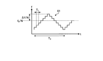
- 4 is a diagram illustrating an example of a signal waveform generated by a reference signal generation unit according to Embodiment 1.
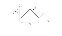
- 6 shows an example of a signal waveform generated by the VCO in Embodiment 1.
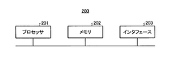
- FIG. 3 is a diagram illustrating an example of a hardware configuration of a processing circuit according to the first embodiment. Diagram for explaining variation of operating point due to individual variation or temperature drift
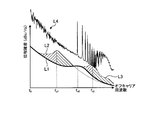
- FIG. 7 is a diagram for explaining fluctuations in PLL cutoff characteristics and phase noise characteristics due to fluctuations in modulation sensitivity.
- FIG. 7 is a view for explaining how the modulation sensitivity approaches a target value by the processing of the flowchart shown in FIG. 7.
- FIG. 4 is a block diagram showing a configuration of a frequency modulation oscillation source according to a second embodiment. Flowchart for explaining the operation of the frequency modulation oscillation source according to the second embodiment The figure which shows an example of the VT table shown in FIG. The figure which shows an example of the VP table shown in FIG.
- FIG. 10 is a view for explaining how the modulation control voltage approaches a target value by the processing of the flowchart shown in FIG. 10.
- FIG. 6 is a block diagram showing a configuration of a frequency modulation oscillation source according to a third embodiment.
- FIG. 15 is a view for explaining how the modulation sensitivity approaches a target value by the processing of the flowchart shown in FIG.
- Flowchart for explaining operation of the frequency modulation oscillation source according to the fourth embodiment First diagram explaining the process of creating V T -V P approximate curve of the fourth embodiment Second diagram explaining the process of creating V T -V P approximate curve of the fourth embodiment Third diagram explaining the process of creating V T -V P approximate curve of the fourth embodiment Time chart for explaining compensation operation of the frequency compensation voltage V T at the time of actual operation when using the method of controlling the frequency modulation oscillator source according to the first to fifth embodiments FIG.
- FIG. 14 is a block diagram showing a configuration of a frequency modulation oscillation source according to a sixth embodiment.
- FIG. 14 is a block diagram showing a configuration of a frequency modulation oscillation source according to a seventh embodiment.
- FIG. 4 is a block diagram showing a configuration of a radar device including any of the frequency modulation oscillation sources described in the first to seventh embodiments.
- FIG. 24 is a block diagram showing a modification of the radar device shown in FIG.
- FIG. 1 is a block diagram showing a configuration of the frequency modulation oscillation source according to the first embodiment.
- FIG. 2 is a diagram illustrating an example of a signal waveform generated by the reference signal generation unit according to the first embodiment.
- FIG. 3 is a diagram illustrating an example of a signal waveform generated by the VCO according to the first embodiment.
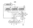
- the frequency modulation oscillation source 100 includes a reference signal generation unit 1, a phase frequency comparison unit (Phase Frequency Detector: PFD) 2, a charge pump (Charge Pump: CP) 3, A loop filter (Loop Filter: LF) 4, VCO 5, frequency divider control unit 6, frequency divider 7, frequency division number setting unit 10, and frequency compensation control unit 30 are provided.
- FIG. 2 shows an example of a divided signal waveform generated by the frequency divider 7 controlled by the frequency divider control unit 6 based on the setting signal of the frequency division number setting unit 10.
- the frequency divider 7 discretely sets the frequency f to f 0 / N ⁇ ⁇ f / N at the first time interval T 1 (where f 0 is the signal of the signal output from the VCO 5).
- center frequency ", Delta] f is" frequency sweep width ", N represents generates a divided signal 68 that is swept in the range of representative) a" division number "periodically at a second time interval T 2.
- T 1 ⁇ T 2 between the first time interval T 1 and the second time interval T 2 .
- first time interval T 1 is set below ⁇ loop time constant of the PLL
- second time interval T 2 is set equal to or larger than ⁇ loop time constant.
- the center frequency f 0 / N of the frequency-divided signal matches the reference signal frequency output from the reference signal generator 1 by the PLL loop.
- the reference signal generator 1 generates the reference signal 61.
- the phase frequency comparator 2 compares the reference signal 61 output from the reference signal generator 1 with the frequency-divided signal 68 output from the frequency divider 7.
- the phase frequency comparing section 2 outputs a comparison result signal 62 corresponding to the phase difference between the reference signal 61 and the frequency-divided signal 68.
- the comparison result signal 62 is a signal in which a frequency difference and a phase difference between the reference signal 61 and the frequency-divided signal 68 are detected.
- the comparison result signal 62 from the phase frequency comparison unit 2 is input to the charge pump 3.
- the charge pump 3 generates a drive current 63 for operating the loop filter 4 based on the comparison result signal 62 and inputs the drive current 63 to the loop filter 4.
- the drive current 63 output by the charge pump 3 is generally called a “charge pump current”.
- the loop filter 4 integrates the electric charge of the driving current 63 supplied from the charge pump 3.
- the loop filter 4 is a low-pass filter for averaging a DC signal including a ripple output from the drive current 63 and converting the signal into a DC signal having a small AC component.
- the loop filter 4 generally includes a passive circuit including a resistor and a capacitor, and an active circuit in which an operational amplifier and the like are combined. Further, the loop filter 4 plays a role in determining a transfer characteristic for stably performing the loop control of the PLL.
- the output of the loop filter 4, as the modulation control voltage V P is input to the VCO 5.
- the VCO 5 is provided with a modulation terminal 50 and a frequency compensation terminal 52.
- the modulation terminal 50, the modulation control voltage V P, which is the first voltage is input.
- the frequency compensation pin 52, a frequency compensation voltage V T is the second voltage is input.
- Oscillation frequency of VCO5 includes a modulation control voltage V P, based on the frequency compensation voltage V T, it is possible to control the frequency at each voltage independently.
- Oscillation frequency of VCO5 includes a modulation control voltage V P output from the loop filter 4 is controlled based on the frequency compensation voltage V T output from the frequency compensation controller 30 to be described later.
- the frequency compensation voltage VT is set to a predetermined value
- the frequency is synchronized with the reference signal 61 output from the reference signal generation unit 1 and the frequency is temporally changed by the frequency division number controlled by the frequency divider control unit 6.
- a changing frequency modulated (FM) signal 65 is output from the VCO 5.
- the frequency division number setting unit 10 outputs a frequency or a frequency division number setting signal corresponding to the frequency to the frequency divider control unit 6 and the frequency compensation control unit 30.
- the frequency divider control unit 6 and the frequency compensation control unit 30 perform frequency division control and frequency calculation described later based on the setting signal.
- the set value of the frequency output from the frequency division number setting unit 10 is one of the setting signals (serial signal) of the PLL operation parameter, and only the frequency (frequency division) setting has a meaning here. This is called the division number setting unit.
- Other PLL operation parameters include modulation parameters such as chirp start frequency, phase, delay time from reference time, chirp signal shape (slope, modulation width), time increment, frequency increment, and number of chirps during product operation.
- setting signals such as a frequency compensation voltage V T related to the PLL operation and a charge pump current Icp described later.
- the frequency divider control unit 6 generates a frequency division control signal 67 for controlling the frequency division number N in the frequency divider 7 based on the setting signal of the frequency division number setting unit 10.
- the feedback signal 66 of the FM signal 65 generated by the VCO 5 is input to the frequency divider 7.
- the frequency divider 7 divides the input feedback signal 66 based on the time set in the frequency division control signal 67 and the frequency division number N, and divides the frequency f of the FM signal 65 by N.
- a frequency-divided signal 68 multiplied by 1 / N is generated and output to the phase frequency comparison unit 2.
- the frequency division control signal 67 has a temporally inverted relationship with respect to the frequency division signal 68 shown in FIG.
- a feedback signal 66 that is the same signal as the FM signal 65 is input to the frequency divider 7.
- a signal obtained by fixedly dividing the frequency of the FM signal 65 is input to the frequency divider 7. Is also good.
- FIG. 3 shows an example of a signal waveform output from the VCO 5 by the PLL control.
- the VCO 5 generates an FM signal 65 whose frequency f changes linearly within a range of f 0 ⁇ ⁇ f, as shown in FIG. Note that the cycle of the FM signal 65 matches the second time interval T2, which is the interval between valleys (or peaks) in the frequency-divided signal 68.
- T2 the second time interval
- FIG. 3 shows a triangular wave (an example in which the frequency f changes linearly with a constant gradient with respect to time) as an example of the FM signal, a chirp signal having a plurality of gradients by PLL control, It is also possible to generate an up-only or down-only chirp signal, or a chirp signal that changes not linearly but in a curved manner (second-order or higher polynomial, exponential function, logarithmic function).
- a frequency compensation control unit 30 is added to suppress phase noise fluctuation due to fluctuation of PLL cutoff characteristics due to individual fluctuation and temperature drift. Have been.
- the frequency compensation control unit 30 forms a “control unit”.
- Frequency compensation control unit 30 by inputting the modulation control voltage V P frequency compensation pin 52 by generating a frequency compensation voltage V T, which is calculated on the basis, and the dividing number N set, V P -f Control is performed to move the operating point of the VCO 5 on the characteristic curve.
- the frequency compensation controller 30 includes a modulation control voltage detector 32, a frequency compensation voltage calculator 33, and a frequency compensation voltage generator 34.
- Modulation control voltage detector 32 monitors the modulation control voltage V P of the loop filter 4 outputs to the modulation terminal 50 of the VCO 5.
- Frequency compensation voltage calculation unit 33 calculates a frequency compensation voltage V T on the basis of the frequency division number N is set detected value of the modulation control voltage detecting unit 32, and the frequency-division control signal 67.
- Frequency compensation voltage generating unit 34 outputs the frequency compensation pin 52 of VCO5 by generating a frequency compensation voltage V T based on the calculated value of the frequency compensation voltage calculation unit 33 has calculated.
- the modulation control voltage detection unit 32 configures a “voltage detection unit”
- the frequency compensation voltage calculation unit 33 configures a “calculation unit”
- the “frequency compensation voltage generation unit 34” configures a “voltage generation unit”. Is constituted.
- FIG. 4 is a diagram illustrating an example of a hardware configuration of the processing circuit 200 according to the first embodiment.
- the processing circuit 200 can be configured to include a processor 201 that performs operations, a memory 202 that stores programs and data read by the processor 201, and an interface 203 that inputs and outputs signals.
- the frequency compensation control unit 30 executes, for example, the processing in which the processor 201 illustrated in FIG. It is realized by executing.
- the function of the frequency compensation control unit 30 may be realized in cooperation with a processor (not shown) that controls the PLL 16. Further, a part of the function of the frequency compensation control unit 30 may be implemented as an electronic circuit, and the other part may be realized using the processor 201 and the memory 202.
- the interface 203 includes an AD converter that converts an analog signal into a digital signal, and a DA converter that converts a digital signal into an analog signal.
- the processor 201 may be an arithmetic unit such as an arithmetic device, a microprocessor, a microcomputer, a CPU (Central Processing Unit), or a DSP (Digital Signal Processor).
- the memory 202 may be a non-volatile or volatile semiconductor memory such as a RAM (Random Access Memory), a ROM (Read Only Memory), a flash memory, an EPROM (Erasable Programmable ROM), an EEPROM (registered trademark) (Electrically EPROM). can do.
- the processor 201 transmits and receives necessary information via the interface 203, executes the program stored in the memory 202, and refers to the table stored in the memory 202. It can be carried out.
- the calculation result of the processor 201 can be stored in the memory 202.
- FIG. 5 is a diagram for explaining a change in an operating point due to individual variation or temperature drift.
- FIG. 6 is a diagram for explaining a change in a PLL cutoff characteristic and a phase noise characteristic due to a change in the modulation sensitivity Kv.
- Kv value the value of the modulation sensitivity Kv is referred to as “Kv value”.
- V P -f characteristic of the VCO becomes a curved characteristic as shown in FIG. 5 shows, in the case of the frequency compensation voltage V T is a constant value, or the tuning voltage terminal V P only, V P -f characteristics at room temperature (f d1) is indicated by the solid line, at high temperature V P - The f characteristic (f d2 ) is indicated by a dashed line, and the V P -f characteristic (f d3 ) at a low temperature is indicated by a broken line.
- the V P -f characteristic of the VCO changes due to the temperature drift.
- the difference in the V P -f characteristics shown in FIG. 5 also appears due to individual variations. That is, due to the individual variation, the V P -f characteristic of the VCO mainly fluctuates in the frequency absolute value on the vertical axis as shown by the curve indicated by f d1 , f d2 , or f d3 in FIG.
- phase margin In a frequency modulation source using a PLL, as long as the phase condition of a PLL loop (hereinafter, referred to as “phase margin”) is satisfied, the oscillation frequency f 0 is locked in a circuit. In a range that satisfies the loop phase margin, a change in Kv is allowed. Therefore, the fluctuation range of the PLL is operable Kv by individual variations or temperature drift, the operating point on the V P -f characteristic varies as shown in FIG.
- the operating point when outputting the oscillation frequency f 0 is P d1
- the V P -f characteristic of the VCO is f d2
- the oscillation frequency f d is P d2
- the operating point when outputting the oscillation frequency f 0 is P d3 .
- a VCO output that changes according to the set frequency division number is shown by a broken line.
- the set frequency division number is a frequency division number set by the frequency division number setting unit 10, controlled by the frequency divider control unit 6, and output by the frequency divider 7.
- the modulation control voltage subjected to frequency division control by the PLL corresponds to the operating points P d1 , P d2 , and P d3 along the respective V P -f characteristic curves.
- the horizontal axis changes as indicated by the thick line in the drawing.
- the slope of the thick line represents the modulation sensitivity Kv.
- the modulation sensitivity Kv is the smallest when the operating point P d2, is greatest when the operating point P d3.
- the modulation sensitivity Kv also changes according to the change in the operating point of the VCO output controlled by the PLL.
- the loop cutoff characteristic (also called “cutoff characteristic”) of the PLL is given by a cutoff frequency.
- the following represents the cut-off frequency "f c”.
- Cut-off frequency f c is the square root of the modulation sensitivity Kv of the operating point of the VCO 5, proportional to the product of the transfer characteristic, and the charge pump current of the loop filter. Therefore, a change in the modulation sensitivity Kv causes a change in the cutoff frequency fc in the PLL loop.
- the cutoff characteristic of the PLL loop fluctuates, the phase noise characteristic deteriorates.
- the time constant ⁇ of the PLL loop described above with respect to the first and second time intervals during the frequency sweep by the PLL in FIGS. 2 and 3 is the reciprocal of fc.
- the horizontal axis of FIG. 6 represents the off carrier frequency when the center frequency f 0 of the coordinate origin, and the vertical axis represents phase noise.
- curve L1 is a PLL cutoff characteristics when a cutoff frequency f c is f c0
- curve L2 is PLL cutoff characteristics when a cutoff frequency of f c1
- curve L3 is cut This is a PLL cutoff characteristic when the off frequency is fc2 .
- the lower side than the cut-off frequency fc is a negative feedback region (hereinafter, referred to as “in the loop band”) of the PLL loop, and the phase is controlled by the free-running phase noise of the VCO suppressed by the negative feedback loop.
- the noise level is determined.
- a higher frequency side than the cutoff frequency fc is a filter region of the PLL loop (hereinafter, referred to as “out of the loop band”), which is affected by noise characteristics of the loop filter 4.
- the phase noise of the PLL is determined by the sum of the noise within the loop band and the noise outside the loop band. For this reason, the design center of the cutoff frequency fc is set in consideration of both levels.
- the design center of the cutoff frequency fc is set in consideration of both levels.
- the design center of the cutoff frequency fc is set in consideration of both levels.
- Relative cut-off frequency f c f c0 corresponding to the modulation sensitivity Kv of the design center, if the modulation sensitivity Kv is smaller than the value of the design center, the cut-off frequency f c is shifted to f c1 lower frequency ,
- the phase noise within the loop band and the filter noise, which is the phase noise outside the loop band, increase. 6, the portion indicated by hatching to the left than f c1 is the phase noise in the loop bandwidth, the portion indicated by hatching to the right than f c1 is a phase noise outside the loop bandwidth.
- phase noise outside the loop bandwidth is increased.
- the PLL loop is unlocked (UNLOCK), and the frequency cannot be controlled.
- the phase noise characteristic is significantly deteriorated, and a large number of spurious components are generated.
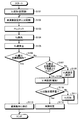
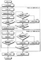
- FIG. 7 is a flowchart for explaining the operation of the frequency modulation oscillation source 100 according to the first embodiment.
- all of the flowcharts in the present embodiment including Embodiments 2 to 4 to be described later, show adjustment steps (hereinafter, appropriately referred to as “adjustments”) performed to suppress deterioration of phase noise characteristics.
- the adjustment of the frequency compensation voltage V T and the charge pump current and the optimization control are performed, and after the adjustment is completed, the operation shifts to a normal PLL modulation operation.
- the frequency compensation voltage VT and the charge pump current are operated at fixed and optimized fixed values within the operation cycle. When an ambient temperature change or the like occurs, the adjustment process is performed again (details will be described later).
- the frequency compensation voltage generating unit 34 to generate a frequency compensation voltage V T is applied to the frequency compensation pin 52 of the VCO 5 (step S101).
- the frequency compensation voltage V T is set in step S101, the initial value of the frequency compensation voltage V T.
- a predetermined center value or the like is set in consideration of the characteristics of the VCO 5.
- the setting value may be a value stored in a memory or the like.
- the division number setting unit 10 and the frequency divider control unit 6 set the oscillation frequency of the VCO 5 near the center of the modulation frequency during normal PLL operation (step S102). For example, when the frequency division number N is set by the frequency division number setting unit 10 and the frequency division control unit 6, the oscillation frequency f of the VCO 5 is synchronized with the reference signal 61 by the PLL loop, and is N times the frequency of the reference signal frequency. Lock to. PLL 16 operates, (step S103) in a state where the modulation frequency is locked in the PLL 16, the modulation control voltage detecting unit 32, the modulation control voltage V P at PLL 16 is detected (step S104). Then, the frequency compensation control unit 30, a known oscillation frequency f is set by the frequency division number N, and based on the detected V P value, to calculate the Kv value (step S105).
- step S104 the two points of the frequency f 1, f 2 in the vicinity of the center of the modulation frequency during normal PLL operation, V P value corresponding to each is detected. That, V P1 is detected V P value when the operating frequency f 1, V P2 is detected V P value when the operating frequency f 2.
- the operating frequencies f 1 and f 2 are set by the frequency division number N given to the frequency divider 7 by the frequency division number setting unit 10 and the frequency divider control unit 6.
- step S105 the frequency compensation control unit 30 calculates a Kv value using the following equation (1).
- the frequency compensation control unit 30 determines whether the Kv value calculated in step S105 is within a target range (step S106). If the calculated Kv value is not a value within the target range (step S106, No), the process proceeds to step S107. In step S107, it is determined whether the Kv value calculated in step S105 is smaller than the lower limit of the target range. If Kv value is smaller than the lower limit of the target range (step S107, Yes), the frequency compensation control unit 30 updates the value of the frequency compensation voltage V T, resets the frequency compensation voltage V T of the updated (hereinafter , Update and reset are collectively referred to as “reset”). Resetting of the frequency compensation voltage V T is performed by increasing the value of the frequency compensation voltage V T previously calculated (step S108).
- step S109 If the Kv value calculated in step S105 is equal to or larger than the lower limit of the target range (No in step S107), the process proceeds to step S109. Since it has been determined in step S106 that the Kv value is not within the target range, the determination of “No” in step S107 is that the Kv value calculated in step S105 is larger than the upper limit of the target range. Means that. Therefore, reconfiguration of the frequency compensation voltage V T at the step S109 is performed by decreasing the value of the frequency compensation voltage V T previously calculated.
- step S107 it is determined whether the Kv value calculated in step S105 is smaller than the lower limit value of the target range. However, it is determined whether the calculated Kv value is larger than the upper limit value of the target range. May be. In this case, when the calculated Kv value is greater than the upper limit of the target range, the frequency compensation control unit 30 resets the frequency compensation voltage V T. Resetting of the frequency compensation voltage V T is performed by decreasing the value of the frequency compensation voltage V T previously calculated. Further, when the calculated Kv value is less than the upper limit of the target range, the frequency compensation controller 30, a new frequency compensation voltage V T which is calculated by increasing the value of the frequency compensation voltage V T previously calculated again Set.
- the frequency compensation control unit 30 determines whether the reset frequency compensation voltage VT is equal to the set limit value (step S110). If the frequency compensation voltage VT is at the set limit value (step S110, Yes), it is determined that a failure has occurred, and the process ends (step S112). On the other hand, when the frequency compensation voltage V T is not set limit value (step S110, No), re-set frequency compensation voltage V T is applied to the frequency compensation voltage generating unit 34. Frequency compensation voltage generating unit 34 to generate the indicated frequency compensation voltage V T, is applied to the frequency compensation pin 52 of the VCO 5 (step S111). After the process in step S111, the process returns to step S102. Thereafter, the processing from step S102 is repeated.
- step S106 if the calculated Kv value is within the target range (step S106, Yes), the process shifts to normal operation and ends (step S113).
- the normal operation is an operation of generating a modulated wave by the PLL 16 based on the frequency division number set by the frequency division number setting unit 10 and controlled by the frequency divider control unit 6.
- the final adjusted frequency compensation voltage V T, the operating point optimal Kv value is obtained, VCO 5 outputs an FM signal 65.
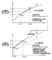
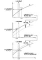
- FIG. 8 is a view for explaining how the modulation sensitivity Kv approaches the target value by the processing of the flowchart shown in FIG.
- the vertical axis represents the frequencies f 1 and f 2 set by the PLL 16 based on the frequency division number set by the frequency division number setting unit 10 and controlled by the frequency divider control unit 6.
- V P value detected by the modulation control voltage detecting unit 32 at each of frequencies f 1, f 2 (V P1 (1), V P2 (1)) are shown.
- the frequencies f 1 and f 2 set near the center frequency f 0 of the modulation frequency during normal operation are locked by the PLL 16.
- P 1 (1) is an operating point for outputting the frequency f 1
- P 2 (1) is an operating point for outputting the frequency f 2 .
- values near the center frequency f 0 are selected.
- Frequency f 1 is smaller than the center frequency f 0, the frequency f 2 is greater than the center frequency f 0.
- Kv value is calculated by the equation (1), if the Kv value within the target range can not be obtained, a new V T value is reset. By the new V T values, how a new Kv value is calculated it is shown in the lower portion of FIG.
- the operating point of the VCO5 moves the curve K2 corresponding to the new V T value. Therefore, the frequency f 1 becomes a P 1 (2) a new operating point on the curve K2, the frequency f 2 is, P 2 on the curve K2 (2) becomes the new operating point.
- the Kv value is calculated. And changing the operating point by re-setting of the V T value, recalculation of Kv value, Kv value which is newly calculated is repeated until a value within the target range. Calculated Kv value, when a value within the target range, the search process of the V T value is ended.
- Last set V T value is in the normal operation, the V T value of the modulation center frequency f 0 of the PLL applied to VCO 5.
- the Kv value calculated last is a Kv value that determines the operating point of the VCO 5 during normal operation.
- the modulation control voltage generated by integrating the comparison result signal corresponding to the phase difference between the reference signal and the frequency-divided signal, and The oscillation frequency of the VCO is controlled based on a frequency compensation voltage set based on the modulation control voltage and the frequency division number. Then, the modulation operation point in the voltage frequency characteristic of the VCO is moved by the frequency compensation voltage, and the frequency compensation voltage is controlled such that the modulation sensitivity at the modulation operation point becomes a value within the target range.
- the frequency modulation oscillation source according to the first embodiment since the cutoff characteristic fluctuation of the PLL can be suppressed, a sufficient operation margin can be obtained with respect to the phase margin in the PLL design. As a result, it is possible to reduce the risk of occurrence of an event that the operating frequency of the PLL is unlocked unexpectedly. Therefore, if the frequency modulation oscillation source according to the first embodiment is applied to a radar device, it is possible to reduce the risk of deviation from radio regulations due to unintended transmission frequency output and radar transmission / reception failure.
- FIG. 9 is a block diagram showing a configuration of a frequency modulation oscillation source 100A according to the second embodiment.
- a frequency compensation voltage table hereinafter, referred to as a “VT table” 40
- a modulation control A voltage table hereinafter, referred to as a “VP table” 42
- a temperature detector 45 is added.
- Other configurations are the same or equivalent to the configurations of the first embodiment, and the same or equivalent components are denoted by the same reference numerals.
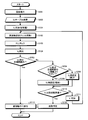
- FIG. 10 is a flowchart for explaining the operation of the frequency modulation oscillation source 100A according to the second embodiment.
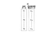
- FIG. 11 is a diagram showing an example of the VT table 40 shown in FIG.
- FIG. 12 is a diagram showing an example of the VP table 42 shown in FIG.
- the same or equivalent processes as those in the flowchart shown in FIG. 7 are denoted by the same step numbers.
- the VT table 40 and the VP table 42 are tables that refer to or store the results calculated by the frequency compensation control unit 30.
- the VT table 40 constitutes a “first table”
- the VP table 42 constitutes a “second table”.
- the VT table 40 and the VP table 42 can be realized using the memory 202 shown in FIG.
- the temperature detector 45 is a detector that detects an ambient temperature. The detection value of the temperature detector 45 is obtained when the frequency compensation control unit 30 reads out the frequency compensation voltage VT and the modulation control voltage VP from each table at the temperature, calculates the VT table 40, and calculates the VT table 40. Is stored in the memory 202. Details of V T tables 40 and V P table 42, and for details of operation when the frequency compensation control unit 30 utilizes a V T tables 40 and V P table 42 will be described later.
- V T table 40 as shown in FIG. 11, the corresponding temperature data (T1, ?? T0, « T2 ) and a frequency compensation voltage data (V T1, ?? V T0, « V T2) and It is a table in which the relationship is described.
- V P table 42 as shown in FIG. 12, the temperature data (T1, ?? T0, « T2 ) and the modulation control voltage data (V P1, ?? V P0, ?? V P2) and Is a table in which the correspondence relationship is described.
- the target range of V P value corresponding to the Kv value of the target range can be obtained by reference to the V P table 42 as shown in FIG. 12.
- Frequency compensation control unit 30 refers to the V T table 40, reads the frequency compensation voltage V T corresponding to the detected ambient temperature (step S202).
- the read frequency compensation voltage VT is provided to the frequency compensation voltage generator 34.
- Frequency compensation voltage generating unit 34 to generate the indicated frequency compensation voltage V T is applied to the frequency compensation pin 52 of the VCO 5 (step S101). Note that, in FIG. 10, the processing from step S101 to step S104 is the same processing as in FIG. 7, and a description thereof will be omitted.
- step S203 Frequency compensation control unit 30, V P value detected in step S104, it is determined whether the value of the target range (step S203). If the detected V P value is not a value within the target range (step S203, No), the process proceeds to step S204.
- step S204 V P value detected in step S104 whether greater than the upper limit of the target range is determined. When V P value is greater than the upper limit of the target range (step S204, Yes), the frequency compensation control unit 30 resets the frequency compensation voltage V T. Resetting of the frequency compensation voltage V T is performed by increasing the value of the frequency compensation voltage V T previously calculated (step S205). Further, if V P value detected in step S104 is equal to or less than the upper limit of the target range (step S204, No), the process proceeds to step S206.
- step S203 since already V P value is determined not to be a value within the target range, the determination of "No" in step S204, the detected V P value lower limit of the target range at step S104 Means less than. Therefore, reconfiguration of the frequency compensation voltage V T at the step S206 is performed by decreasing the value of the frequency compensation voltage V T previously calculated.
- step S110 The processing from step S110 to step S112 is the same processing as in FIG. 7, and the description here is omitted.
- step S204 although V P value detected in step S104 is determined whether greater than the upper limit of the target range, whether the detected V P value is smaller than the lower limit of the target range May be determined. In this case, if the detected V P value is smaller than the lower limit of the target range, the frequency compensation control unit 30 resets the frequency compensation voltage V T. Resetting of the frequency compensation voltage V T is performed by decreasing the value of the frequency compensation voltage V T previously calculated. Further, if the detected V P value is more than the lower limit of the target range, the frequency compensation controller 30, a new frequency compensation voltage V T which is calculated by increasing the value of the frequency compensation voltage V T previously calculated Reset.
- the target range of V P value grasps the V P -f characteristic of VCO5 shown in FIG. 5, previously obtained in advance by an initial adjustment.
- the modulation sensitivity Kv value may be determined as described in the first embodiment, and the modulation sensitivity Kv value may be determined from the Kv value that is the design center of the PLL loop characteristic.
- V P -kv characteristics varactor characteristics are not fluctuated in individuals is approximately constant, is possible not greater variation with temperature I know it.
- FIG. 10 is a diagram for explaining a state approaching the value of the modulation control voltage V P is targeted by the process of the flowchart shown in FIG. 10.
- the vertical axis is shown the center frequency f 0 that is set by the PLL 16, the horizontal axis, V P value detected (V P (1)) are shown.
- P 0 (1) is an operating point for outputting the center frequency f 0 in the curve K1 representing the V P ⁇ f characteristic.
- Curve K1 is determined by the initial value of the frequency compensation voltage V T.
- VP (1) does not fall within the VP value target range indicated by hatching. Therefore, a new VT value is reset. The manner in which the new VT value is reset is shown in the middle part of FIG.
- the operating point of the VCO5 moves on a curve K4 corresponding to the new V T value.
- the center frequency f 0 is locked by the PLL 16.
- P 0 (3) on the curve K3 is a new operating point.
- P 0 V P values in (3) (V P (3 )) is contained in V P value target range.
- the last set V T value is in the normal operation, the V T value of the modulation center frequency f 0 of the PLL applied to VCO 5.
- the operating point of the VCO 5 is an operating point at which an optimum Kv value is obtained.
- the flowchart of FIG. 10 in the second embodiment and the adjustment flow of the frequency compensation voltage V T and stores the value calculated and determined by the adjustment flow V T table 40, at the time of subsequent adjustment time or operational it may be referred to as a monitoring of the frequency compensation voltage V T.
- the detected V P value V stored in the P table 42 may be a reference for the modulation control voltage V P at the time of subsequent adjustment time or operation.
- the VT table 40 and the VP table 42 set upper and lower limits with a predetermined width for the adjustment results, and monitor whether or not the temperature falls within the upper and lower limits at each temperature during operation. It may be. In this way, the effect of shortening the adjustment time in the next adjustment flow can be obtained.
- frequency compensation voltage VT is controlled such that modulation control voltage VP has a value within a target range.
- the frequency modulation oscillation source according to the second embodiment fluctuations in the cut-off characteristics of the PLL can be suppressed, so that a sufficient operation margin can be obtained with respect to the phase margin in the PLL design. As a result, it is possible to reduce the risk of occurrence of an event that the operating frequency of the PLL is unlocked unexpectedly. Therefore, if the frequency modulation oscillation source according to the first embodiment is applied to a radar device, it is possible to reduce the risk of deviation from radio regulations due to unintended transmission frequency output and radar transmission / reception failure.
- FIG. 14 is a block diagram showing a configuration of the frequency modulation oscillation source according to the third embodiment.
- frequency compensation control section 30 is changed to frequency compensation control section 30A in the configuration of frequency modulation oscillation source 100 according to the first embodiment shown in FIG. Have been.
- the signal switch 8 is added to the PLL 16 in the first embodiment shown in FIG. 1 to constitute a PLL 16A. Further, a frequency detection unit 31 is added.
- a signal changeover switch 8 is provided between the loop filter 4 and the VCO 5, and an output of the signal changeover switch 8 is input to the VCO 5.
- a frequency compensation voltage / modulation control voltage calculator 35 and a modulation control voltage generator 36 are added in place of the modulation control voltage detector 32 and the frequency compensation voltage calculator 33.
- a frequency detection unit 31 is provided, and the frequency detected by the frequency detection unit 31 is input to the frequency compensation voltage and modulation control voltage calculation unit 35. Therefore, in FIG. 14, the output of the frequency division number setting unit 10 is not input to the frequency compensation voltage and modulation control voltage calculation unit 35 but is input only to the division period control unit 6.
- the other configuration is the same as or equivalent to the configuration of the first embodiment, and the same or equivalent components are denoted by the same reference numerals and redundant description will be omitted.
- the frequency compensation control unit 30A is the output frequency of the VCO 5 at the time of the modulation control voltage V P of the frequency compensation control unit 30A has generated is input to the VCO 5, read from the frequency detector 31.
- the output frequency of the VCO 5 is detected by the frequency detector 31 from the reference signal 61 and the feedback signal 66.
- This repetition, frequency compensation control unit 30A finds out the operating point of VCO5 target Kv value is obtained on the V P -f characteristic curve, performs control to move the operating point.
- the frequency compensation control unit 30A is input to the frequency compensation pin 52 by generating a frequency compensation voltage V T, similarly the output frequency from the reference signal 61 and feedback signal 66 frequency detecting unit 31 is input VCO5 To detect.
- the frequency compensation control unit 30A includes a frequency compensation voltage and modulation control voltage calculation unit 35, a frequency compensation voltage generation unit 34, and a modulation control voltage generation unit 36.
- the frequency detection unit 31 configures a “detection unit”
- the frequency compensation voltage and modulation control voltage calculation unit 35 configures a “calculation unit”
- the modulation control voltage generation unit 36 configures a “first voltage”.
- a frequency compensation voltage generator 34 as a “second voltage generator”.
- Modulation control voltage generating unit 36 generates a modulation control voltage V P to be input to the modulation terminal 50 of the VCO 5.
- Modulation control voltage V P to be input to the modulation terminal 50 of VCO5 is inputted via the signal changeover switch 8.
- Signal changeover switch 8 the receiving a first terminal 8a for receiving a modulation control voltage V P output from the loop filter 4, a modulation control voltage V P output from the modulation control voltage generating unit 36 of the frequency compensation control unit 30A And two terminals 8b.
- the signal changeover switch 8 is switched to the first terminal 8a side, to PLL operation the VCO 5.
- the frequency compensation control unit 30A switches the signal changeover switch 8 to the second terminal 8b side, PLL The loop is disconnected from the VCO 5, and the VCO 5 is independently operated in the open loop.
- the signal changeover switch 8 switches the modulation control voltage V P is a first voltage input to VCO5 outputted from the loop filter 4, the third voltage output from the modulation control voltage generating unit 36 constitute a "voltage switching unit" for inputting the certain modulation control voltage V P to the VCO 5.
- the frequency compensation voltage and the modulation control voltage calculation unit 35 respectively a frequency compensation voltage V T and the modulation control voltage V P is set as an initial value, the output from the frequency compensation voltage generating unit 34 and the modulation control voltage generating unit 36 Then, it is input to the VCO 5.
- the frequency detection unit 31 is based on the output signal of the VCO 5 at each of the input voltages, that is, the feedback signal 66 output to the frequency divider 7 and the reference signal 61 output to the phase frequency comparison unit 2 by the reference signal generation unit 1. Then, the oscillation frequency of the VCO 5 is detected.
- the frequency compensation voltage and modulation control voltage calculator 35 calculates the detection value of the frequency detector 31, that is, the oscillation frequency of the VCO 5 detected by the frequency detector 31 and the modulation control voltage V P output from the modulation control voltage generator 36. , The modulation sensitivity Kv is calculated. When the target of the modulation sensitivity Kv is not obtained, the frequency compensation voltage and the modulation control voltage calculation unit 35 sets the following modulation control voltage V P, and enter into VCO5 output from the modulation control voltage generating unit 36, again , The modulation sensitivity Kv is calculated. Or more repeat, the goal of the modulation sensitivity Kv calculates the modulation control voltage V P to be obtained. In the process up to calculate the above modulation control voltage V P, the frequency compensation voltage V T is maintained at the initial value.
- the frequency at this time is detected by the frequency detection unit 31.
- the frequency compensation voltage V T of the target frequency is obtained is calculated.
- the target frequency of the VCO 5 is selected so as to be the center frequency during normal PLL operation, that is, during modulation.
- the frequency compensation voltage V T which is determined by the adjustment of the above, is set by the frequency compensation voltage and the modulation control voltage calculation unit 35, is input from the frequency compensation voltage generating unit 34 for frequency compensation terminal 52 of VCO5 You.
- Frequency compensation control unit 30A switches the signal changeover switch 8 to the first terminal 8a side, a modulation control voltage V P is inputted from the loop filter 4 in VCO 5, to PLL operation the PLL 16a.
- PLL16A is the setting frequency compensation voltage V T by adjusting the output frequency and modulation sensitivity Kv to PLL operation at the target value.
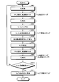
- FIG. 15 is a flowchart for explaining the operation of the frequency modulation oscillation source 100B according to the third embodiment.
- V P value corresponding to the Kv value of the target is not known in advance.
- V P value summary may set the V P value as an initial value.
- a frequency compensation voltage generating unit 34 applies the initial value of the frequency compensation voltage V T to the frequency compensation pin 52 of the VCO 5 (step S301). Then, the modulation control voltage generator 36 via the signal changeover switch 8, and applies a modulation control voltage V P to the modulation terminal 50 of the VCO 5 (step S302).
- the frequency detector 31 detects the oscillation frequency of the VCO 5 (Step S303). The detection of the applied and the oscillation frequency of the modulation control voltage V P is carried out in at least two points.
- Frequency compensation control unit 30A includes a modulation control voltage V P applied at step S302, based on the oscillation frequency f detected in step S303, calculates the Kv value (step S304).
- the frequency compensation control unit 30A determines whether the Kv value calculated in step S304 is within a target range (step S305). If the calculated Kv value is not within the target range (No at Step S305), the process proceeds to Step S306. In step S306, it is determined whether the Kv value calculated in step S304 is smaller than the lower limit of the target range. If Kv value is smaller than the lower limit of the target range (step S306, Yes), the frequency compensation control unit 30A updates the value of the modulation control voltage V P, resets the modulation control voltage V P of the updated. Resetting of the modulation control voltage V P is performed by decreasing the value of the modulation control voltage V P previously calculated (step S307).
- step S306 If the Kv value calculated in step S304 is equal to or larger than the lower limit of the target range (step S306, No), the process proceeds to step S308. Since it is determined in step S305 that the Kv value is not within the target range, the determination of “No” in step S306 is that the Kv value calculated in step S304 is larger than the upper limit of the target range. Means that. Therefore, resetting of the modulation control voltage V P at the step S308 is performed by increasing the value of the modulation control voltage V P previously calculated.
- step S306 it is determined whether the Kv value calculated in step S304 is smaller than the lower limit of the target range. However, it is determined whether the calculated Kv value is larger than the upper limit of the target range. May be. In this case, when the calculated Kv value is greater than the upper limit of the target range, the frequency compensation control unit 30A resets the modulation control voltage V P. Resetting of the modulation control voltage V P is performed by increasing the value of the modulation control voltage V P previously calculated. Further, when the calculated Kv value is less than the upper limit of the target range, the frequency compensation controller 30, a new modulation control voltage V P which is calculated by reducing the value of the modulation control voltage V P previously calculated again Set.
- the frequency compensation control unit 30A determines whether the reset modulation control voltage VP is at the set limit value (step S309). If the modulation control voltage VP is at the set limit value (step S309, Yes), it is determined that a failure has occurred, and the process ends (step S318). On the other hand, if the modulation control voltage V P is not set limit value (step S309, No), the flow returns to step S302. Thereafter, the processing from step S302 to step S309 is repeated.
- the reset modulation control voltage VP is supplied to the modulation control voltage generator 36. Modulation control voltage generating unit 36 generates a designated modulation control voltage V P, applied to the modulation terminal 50 of VCO5 via the signal changeover switch 8.
- step S305 if the calculated Kv value is within the target range (step S305, Yes), the process proceeds to step S310.
- the processing from step S302 to step S309 is the adjustment step of the modulation control voltage V P by Kv value (determination step).
- the modulation control voltage V P that gives the Kv value within the target range is determined.
- Modulation control voltage generation unit 36 applies to the modulation terminal 50 of VCO5 decision value of the modulation control voltage V P via the signal changeover switch 8.
- the modulation control voltage V P applied here is different from the modulation control voltage V P applied at step S302, a value of one point center.
- the process proceeds to step S311.
- step S311 under the condition that the modulation control voltage V P which is determined in step S305 is applied to the modulation terminal 50 of the VCO 5, the frequency compensation voltage generating unit 34, frequency compensation of the VCO 5 frequency compensation voltage V T To the terminal 52.
- the frequency detector 31 detects the oscillation frequency of the VCO 5 (Step S312).
- the frequency compensation control unit 30A determines whether the frequency detected in step S312 is within a target range (step S313). If the detected frequency is not a value within the target range (step S313, No), the process proceeds to step S314. In step S314, it is determined whether the frequency detected in step S312 is larger than the upper limit of the target range. If the detected frequency is greater than the upper limit of the target range (step S314, Yes), the frequency compensation control unit 30A updates the value of the frequency compensation voltage V T, resets the value of the updated. Resetting of the frequency compensation voltage V T is performed by decreasing the value of the frequency compensation voltage V T previously calculated (step S315).
- step S312 If the frequency detected in step S312 is equal to or lower than the upper limit value of the target range (step S314, No), the process proceeds to step S316. Since it is determined in step S313 that the frequency already detected is not a value within the target range, the determination of “No” in step S314 is that the frequency detected in step S312 is smaller than the lower limit of the target range. It means big. Therefore, reconfiguration of the frequency compensation voltage V T at the step S316 is performed by increasing the value of the frequency compensation voltage V T previously calculated.
- step S314 it is determined whether the frequency detected in step S312 is higher than the upper limit of the target range. However, it is determined whether the detected frequency is lower than the lower limit of the target range. Is also good. In this case, if the detected frequency is smaller than the lower limit of the target range, the frequency compensation control unit 30A resets the frequency compensation voltage V T. Resetting of the frequency compensation voltage V T is performed by increasing the value of the frequency compensation voltage V T previously calculated. Further, if the detected frequency above the lower limit of the target range, the frequency compensation control unit 30A is reset and a new frequency compensation voltage V T which is calculated by reducing the value of the frequency compensation voltage V T previously calculated I do.
- the frequency compensation control unit 30A determines whether or not the reset frequency compensation voltage VT is at the set limit value (step S317). If the frequency compensation voltage V T is set limit value (step S317, Yes), it terminates the malfunction determination to process (step S318). On the other hand, when the frequency compensation voltage V T is not set limit value (step S317, No), the flow returns to step S311. Thereafter, the processing from step S311 to step S317 is repeated.
- the reset frequency compensation voltage VT is provided to the frequency compensation voltage generator 34. Frequency compensation voltage generating unit 34 generates a designated frequency compensation voltage V T, is applied to the frequency compensation pin 52 of the VCO 5.
- step S313 if the frequency detected in step S312 is within the target range (step S313, Yes), the process shifts to normal operation and ends (step S319).
- the processing from step S311 to step S317 is the adjustment step of the frequency compensation voltage V T by the frequency (determining step).
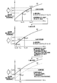
- FIG. 16 is a view for explaining how the modulation sensitivity Kv approaches the target value by the processing of the flowchart shown in FIG.
- the vertical axis the oscillation frequency f 1 of VCO5 controlled by the modulation control voltage V P (1) and f 2 (1) is shown in the horizontal axis
- V P is set
- the values (V P1 (1), V P2 (1)) are shown.
- P 1 (1) is an operating point for outputting the oscillation frequency f 1 (1)
- P 2 (1) is an operating point for outputting the oscillation frequency f 2 (1).
- P 0 (1) is an operating point for outputting the oscillation frequency f 0 (1) located between the oscillation frequency f 1 (1) and the oscillation frequency f 2 (1) in the curve K5.
- the Kv value is calculated by the following equation (2).
- Kv value is calculated by the equation (2), if the Kv value within the target range can not be obtained, a new V P value is calculated. By the new V P values, how a new Kv value is calculated it is shown in the middle portion of FIG. 16.
- the operating point of VCO5 P 0 (1) is moved to the operation point corresponding to the new V P value P 0 (2).
- P 1 (2) corresponding to V P1 (2) and P 2 (2) corresponding to V P2 (2) are new operating points.
- the frequency detection unit 31 the frequency f 1 (2) in the new operating point P 1 (2), and the frequency f 2 in the new operating point P 2 (2) (2) is detected.
- the Kv value at the new operating point is calculated by the following equation (3).
- the change of the operating point and the recalculation of the Kv value are repeated until the newly calculated Kv value becomes a value within the target range.
- Calculated Kv value when a value within the target range, the search processing of V P value is ended.
- the finally calculated Kv value is a Kv value that determines the operating point of the VCO 5 during normal operation, and corresponds to the operating point P 0 (2) in the middle part of FIG. P 0 (2) is an operating point for outputting the oscillation frequency f 0 (2) at the modulation control voltage V P0 .
- V T value is a set value of the frequency compensation voltage V T is performed. How search for V T value is performed is shown in the lower portion of FIG. 16.
- the operating point P 0 (2) on the curve K5 is the same as P 0 (2) shown in the middle part of FIG. 16, and the oscillation frequency f 0 (2) at the modulation control voltage V P0 . ) Is output.
- the frequency compensation voltage VT is reset so that a target frequency that is a frequency within the target range is obtained.
- V P -f characteristic of VCO5 controlled by new frequency compensation voltage V T is represented by a curve K6.
- P 0 (3) in the curve K6 is an operating point for outputting the oscillation frequency f 0 (3).
- the oscillation frequency f 0 (3) at the operating point P 0 (3) is within the target range. Incidentally, when the target frequency is not obtained, until the target frequency is obtained, the process of searching the frequency compensation voltage V T is performed.
- the Kv value at the operating point P 0 (2) and the Kv value at the operating point P 0 (3) are operating points determined by the same modulation control voltage V P0 , and both have substantially the same value. However, in order to know the exact Kv value, the final frequency compensation voltage V T After determining it may be performed calculation of the Kv value.
- V P value was finally determined by the flow and Kv value of 15, may be stored in the memory 202 shown in FIG. 4, may be stored in V P table 42 shown in FIG. 9 .
- the method described in the first or second embodiment can be applied to the next VT value search process.
- an effect of shortening the search time can be expected.
- the modulation control voltage VP and the frequency compensation voltage VT are controlled such that the modulation sensitivity Kv (Kv value) falls within a target range.
- the method according to the third embodiment it is possible to enter the VCO 5 disconnect the PLL loop from VCO 5 is independent operation, the modulation control voltage V P output from the frequency compensation controller 30A to VCO 5.
- the V P value corresponding to the Kv value of the target is not known in advance, it is possible to search for V P value for obtaining the Kv value of the target.
- the frequency modulation oscillation source according to the third embodiment since a change in the cutoff characteristic of the PLL can be suppressed, a sufficient operation margin can be obtained with respect to the phase margin in the PLL design. As a result, it is possible to reduce the risk of occurrence of an event that the operating frequency of the PLL is unlocked unexpectedly. Therefore, if the frequency modulation oscillation source according to the third embodiment is applied to a radar device, it is possible to reduce the risk of deviation from radio regulations due to unintended transmission frequency output and radar transmission / reception failure.
- FIG. 17 is a flowchart for explaining the operation of the frequency modulation oscillation source according to the fourth embodiment.
- Figure 18 is a first diagram for explaining the process of creating V T -V P approximate curve in the fourth embodiment.
- Figure 19 is a second diagram explaining the process of creating V T -V P approximate curve in the fourth embodiment.
- Figure 20 is a third diagram explaining the process of creating V T -V P approximate curve in the fourth embodiment.
- the function of the frequency modulation oscillation source according to the fourth embodiment can be realized with the same or equivalent configuration as that of the first embodiment shown in FIG.
- V P verification step may be in place is referred to as Kv verification step.
- V P detection step consists of three steps from step S401 to step S403.
- the VT (T) calculation step includes three steps from step S404 to step S406.
- V T (T) calculation step is a step of calculating the V T (T) is a frequency compensation voltage V T for obtaining a V P value of the target.
- V P verification step consists of four steps from step S407 to step S410.
- V P verification step steps of applying V T obtained in V T (T) calculation step (T) is the VCO 5, that V P value of the target is obtained and verified by actually detected It is. If V T (T) V T which is calculated by the calculation step (T) shall be feasible, V P verification step may be omitted.
- Step S411 is a V T (T) update step.
- the frequency compensation voltage generator 34 applies the frequency compensation voltage VT to the frequency compensation terminal 52 (Step S401).
- PLL 16 operates, frequency is locked at the modulation center frequency f 0 in the normal operation (step S402).
- the modulation control voltage detecting unit 32 detects the modulation control voltage V P (step S403). Specific examples of these steps will be described with reference to the example of FIG.
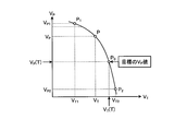
- FIG. 18 shows four curves K7, K8, K9, and K10 representing the V P -f characteristics.
- the initial operating point that is, the operating point at the start of compensation is the point P on the curve K7.
- V P is detected.
- the example of FIG. 18 is an example in the case where there are three operating points. As shown in FIG. 18, when the V T V T1 value is less than is applied, the operating point becomes P 1 point on the curve K8, V P1 is detected. Also, if V T2 also is greater than V T is applied, the operating point becomes P 2 points on the curve K9, V P2 is detected. In the example of FIG.
- Kv value of P 0 point on the curve K10 is the target, i.e., are shown as operating point giving the Kv value within the target range.
- step S404 a frequency compensation voltage V T was applied at step S401, on the basis of the detected modulation control voltage V P at step S403, a process of mapping these (hereinafter, " V T is referred to as -V P mapped ") is performed (step S404).
- V T is referred to as -V P mapped .
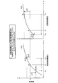
- FIG. 19 separately shows the relationship between the frequency compensation voltage VT and the frequency f, and the relationship between the modulation control voltage VP and the frequency f.
- the oscillation frequency of the VCO 5 is set by the frequency division number setting unit 10 and locked to the frequency f 0 corresponding to the frequency division number controlled by the frequency divider control unit 6. Therefore, the frequency compensation voltage V T and the modulation control voltage V P changes in balance with each other. Therefore, the oscillation frequency of the VCO 5 remains at f0 within the range in which the PLL 16 operates. This can be explained with the contents shown in the next section.
- the frequency difference between the operating point P and the operating point P 3 (P 1 ) in the curve K11 in the left diagram is the operating point P and the operating point in the curve K12 in the right diagram. coincides with the frequency difference between the P 1.
- the frequency compensation voltage is changed from V T to V T2, the oscillation frequency of VCO5 acts in the direction to rise only .DELTA.f2.
- the PLL operation in a state in which frequency compensation voltage is changed from V T to V T2 acts in a direction in which the oscillation frequency of the VCO 5 is lowered by .DELTA.f2, change modulation operating point of the VCO 5, modulation control voltage is changed from V P to V P1.
- the frequency difference between the operating point P in the curve K11 in the left side of FIG operating point P 2 is the operating point P in the curve K12 in the right side of FIG operating point P 2 Match the frequency difference between
- V T -V P mapping process data (hereinafter, “(V T , V P) ” is a pair of the frequency compensation voltage V T applied to the VCO 5 and the modulation control voltage V P detected at that time. ) ”).
- the frequency compensation control unit 30 based on collected in the process of step S404 (V T, V P), V T representing the relationship between the frequency compensation voltage V T and the modulation control voltage V P - A VP approximate curve is created (step S405). Then, the frequency compensation controller 30 uses the V T -V P approximated curve generated in step S405, calculates a frequency compensation voltage V T for obtaining a V P value of the target (T) (step S406 ). Specific examples of the processing of these steps will be described with reference to the example of FIG.
- FIG. 20 shows an example of V T -V P approximation curves are shown.
- V T -V P approximate curve shown in Figure 20 three data pairs collected in the process of step S404 (V T, V P) , the (V T1, V P1) and (V T2, V P2) The three data pairs are plotted and connected by a curve.
- V T corresponding to V P (T) (T) becomes the frequency compensation voltage V T for obtaining a V P value of the target.
- V T -V P approximate curve frequency compensation voltage V T for obtaining a V P value of target (T) can be calculated directly.
- the frequency compensation voltage generator 34 applies the frequency compensation voltage V T (T) calculated in step S406 to the frequency compensation terminal 52 (step S407).
- the frequency compensation control unit 30 causes the VCO 5 to perform a PLL operation at the frequency f 0 corresponding to the frequency division number set by the frequency division number setting unit 10 and controlled by the frequency divider control unit 6, and the oscillation of the VCO 5 The frequency is locked (step S408).
- the oscillation frequency of VCO5 at this time the frequency f 0 which is set at 18 and 19.
- Modulation control voltage detecting unit 32 detects the modulation control voltage V P at which VCO5 is locked to the frequency f 0 (step S409).
- the frequency compensation control unit 30 determines whether or not the detected VP value is within a target range (Step S410).
- step S410 If the detected V P value is not a value within the target range (step S410, No), the flow returns to step S401.
- Frequency compensation control unit 30 discards the V T -V P approximated curve generated in step S405, creates a new V T -V P trendline.
- step S410 if the detected VP value is within the target range (step S410, Yes), the frequency compensation voltage V T (T) calculated in step S406 is reflected in the memory 202, and the process ends (step S410). S411).
- the modulation control voltage V P at the time of frequency locked To detect. Then, to create a V T -V P approximate curve based the applied frequency compensation voltage V T, and the detected modulation control voltage V P. Then, based on V T -V P approximated curve generated, to calculate a frequency compensation voltage V T for obtaining a V P value of the target. Thereby, the modulation sensitivity Kv is controlled to be a value within the target range.
- a frequency compensation voltage V T calculated in the above process is applied to the VCO, that V P value of the target is obtained, the actual Includes the steps of detecting and verifying. Therefore, this verification step may be selected and executed as necessary. Executing the verification step has the effect of ensuring that the target VP value is obtained.
- Embodiment 5 the target of the Kv value and V P value, a description will be given of a control in a case where the frequency compensation voltage V T exceeds the set limit value.
- the control according to the present embodiment can be executed by the frequency compensation control unit 30 or the frequency compensation control unit 30A.
- the charge pump current output from the charge pump 3 to the loop filter 4 is not controlled. Therefore, in the fifth embodiment, when the frequency compensation voltage V T is determined to exceed the set limit value, controls the charge pump current, resetting Kv value for the target, and V P value a target Then, the frequency compensation voltage VT is adjusted.
- the charge pump current is appropriately described as “Icp”.
- the PLL loop characteristic (fc characteristic) that affects the phase noise characteristic of the PLL is proportional to the product of the square root of the Kv value, the transfer function of the loop filter 4, and Icp.
- the transfer function of the loop filter 4 is determined by the resistance value of the resistance constituting the loop filter 4, the capacitance value of the capacitor, the GBW (product of open loop gain and frequency) of the operational amplifier, and the like. It is uniformly determined as a circuit constant. Therefore, the Kv value and Icp are used as control parameters.
- Kv 1 the Kv value (hereinafter referred to as “Kv 1 ”) as a new target value is calculated based on the following equation (4). to calculate the corresponding Icp 1.
- Icp 1 ⁇ (Kv 0 / Kv 1 ) ⁇ Icp 0 (4)
- the frequency modulation oscillation source when the frequency compensation voltage V T is determined to be set limit value calculates the Kv value when it is determined that exceeds the set limit value, The charge pump current is calculated based on the calculated Kv value and the newly set target Kv value. Then, a charge pump current based on the calculated value of the charge pump current, that is, a new drive current level in the charge pump 3 is set, and a charge pump current having the set drive current level is generated to drive the loop filter 4.
- a target it is possible to adjust and re-set the Kv value and V P value, within the setting limits of the frequency compensation voltage V T, Kv value and V P value to target obtained There is an effect that it can be.
- FIG. 21 is a time chart for explaining compensation operation of the frequency compensation voltage V T at the time of actual operation when using the method of controlling the frequency modulation oscillator source according to the first to fifth embodiments.
- FIG. 21 shows waveforms of main parts related to a control (adjustment) method during the actual operation of the frequency modulation oscillation source according to the first to fifth embodiments.
- (1) PLL operation setting signal, (2) modulation (normal operation) start trigger, (3) VCO output signal (frequency), (4) VT output (setting), (4) 5) Icp setting are shown the waveforms of the (6) V P output.
- the PLL operation setting signal and the modulation (normal operation) start trigger are a PLL operation parameter setting signal (serial signal) output from the processor 201 and a reference timing signal.
- the VCO output signal (frequency) is set by the frequency division number setting unit 10 according to the reference timing signal, and is controlled by the frequency divider control unit 6 into a frequency division signal 68 that is swept based on the frequency division number and time. Output correspondingly.
- V T output is set on the basis of the PLL operation setting signal, time waveform, Icp set of frequency compensation voltage V T applied from the frequency compensation voltage generating unit 34 for frequency compensation terminal 52 of VCO5 Is a charge pump current set for the charge pump 3 based on the PLL operation setting signal.
- V P output in the above PLL operation, the output from the loop filter 4, a time waveform of the modulation control voltage to frequency sweep the VCO 5.
- V T the adjustment frequency compensation voltage
- Icp setting shows an example in which the invariant.
- the PLL is started at time t0 when the PLL operation setting signal falls, and locked at time t1.
- a modulation start trigger is input at time t2, and the modulation mode starts at time t3 when the modulation start trigger falls.
- a frequency divider setting signal whose frequency changes linearly with time is generated.
- a period from time t3 to time t4 is an output period of the FM signal.
- a period from time t4 to time t5 is an output section of a fixed frequency CW signal in which FM modulation is not performed.
- the period from time t5 to time t6 is a period during which the FM signal is not transmitted from a transmission amplifier (not shown) located downstream of the frequency modulation oscillation source of the present application (hereinafter, referred to as a “signal non-transmission period”).
- the signal non-transmission period is a period different from the period during which the normal operation in the actual operation is performed.
- Kv compensation is performed using the signal non-transmission period.
- the processing from step S401 to step S410 or the processing from step S401 to step S406 is executed during the signal non-transmission period.
- Kv compensation i.e. adjusted, optimized controlled V T
- Icp charge pump current
- the PLL operation setting signal includes a control signal such as a frequency compensation voltage V T for performing Kv compensation and a charge pump current Icp.
- V T is the time when the next modulation start trigger falls.
- the operation cycle is from time t3 to time t7.
- V P variation during PLL operation generated by the change of such ambient temperature, i.e. against Kv variation of VCO (the period from time t4 to time t6)
- V P fluctuates i.e. Kv variation of the VCO is compensated to the original value.
- Kv compensation can be performed during actual operation. For this reason, it is also effective in suppressing a change in the Kv value of the VCO due to aging.
- FIG. 22 is a block diagram showing a configuration of the frequency modulation oscillation source according to the sixth embodiment.
- a direct digital signal is provided between the reference signal generator 1 and the phase frequency comparator 2 in the configuration of the first embodiment shown in FIG.
- a synthesizer (Direct ⁇ Digital ⁇ Synthesizer: DDS) 9 is provided.
- the DDS 9 is a circuit that includes an adder, a latch circuit, a ROM, a DA converter, and the like, and digitally generates an arbitrary signal waveform or an arbitrary frequency signal by discrete sampling processing.
- the phase frequency comparison unit 2, charge pump 3, loop filter 4, VCO 5, frequency divider 7, and DDS 9 constitute a PLL 16B.
- FIG. 22 is different from that of FIG. 1 in that the configuration does not include the frequency divider control unit 6.
- the frequency modulation oscillation source 100C includes the DDS 9 arranged before the phase frequency comparison unit 2.
- the DDS 9 generates the DDS reference signal 71 input to the phase frequency comparison unit 2 using the reference signal 61 output from the reference signal generation unit 1 and the frequency (division number) set value of the frequency division number setting unit 10. I do.
- DDS reference signal 71 is discretely swept in a first time interval T 1 of the following loop time constant, periodic loop time constant ⁇ over a second time interval T 2, linearly relative to and time This is a reference signal whose frequency changes. That is, the DDS reference signal 71 is a second reference signal that changes a frequency set with respect to time based on the input reference signal 61 as the first reference signal.
- the phase frequency comparison unit 2 generates a comparison result signal 62 corresponding to the phase difference between the DDS reference signal 71 and the frequency-divided signal 68 output from the frequency divider 7 and sends it to the loop filter 4. Subsequent operations are as described above.
- the frequency modulation oscillation unit 100C includes the frequency compensation control unit 30 as in the first embodiment shown in FIG. Therefore, by using the method described in Embodiment 1, Embodiment 2, or Embodiment 4, the same effect as in Embodiment 1, Embodiment 2, or Embodiment 4 can be obtained.
- the configuration in which the DDS 9 is provided between the reference signal generation unit 1 and the phase frequency comparison unit 2 is applied to FIG. 1, but this configuration is applied to the configuration of the second embodiment shown in FIG. This configuration may be applied, or this configuration may be applied to the configuration of the third embodiment shown in FIG.
- the same effect as in the third embodiment can be obtained.
- FIG. 23 is a block diagram showing a configuration of the frequency modulation oscillation source according to the seventh embodiment.
- a DDS 9 is provided between the phase frequency comparison unit 2 and the frequency divider 7 in the configuration of the first embodiment shown in FIG. Can be
- the phase frequency comparator 2, the charge pump 3, the loop filter 4, the VCO 5, the frequency divider 7, and the DDS 9 constitute a PLL 16C.
- FIG. 23 The configuration of FIG. 23 is different from that of FIG. 1 in that the configuration does not include the frequency divider control unit 6.
- the phase frequency comparison unit 2 Is generated.
- DDS division signal 72 is discretely swept in a first time interval T 1 of the following loop time constant, linear with respect to periodic and time loop time constant ⁇ or more second time interval T 2 Is a frequency-divided signal whose frequency changes. That is, the DDS frequency-divided signal 72 is a second frequency-divided signal that changes in frequency set with respect to time based on the frequency-divided signal 68 that is the first frequency-divided signal output from the frequency divider 7. It is.
- the phase frequency comparison unit 2 generates a comparison result signal 62 corresponding to the phase difference between the DDS frequency-divided signal 72 and the reference signal 61 output from the reference signal generation unit 1, and sends the comparison result signal 62 to the loop filter 4. Subsequent operations are as described above.
- the frequency compensation oscillation unit 30 is provided, as in the first embodiment shown in FIG. Therefore, by using the method described in Embodiment 1, Embodiment 2, or Embodiment 4, the same effect as in Embodiment 1, Embodiment 2, or Embodiment 4 can be obtained.
- the configuration in which the DDS 9 is provided between the phase frequency comparison unit 2 and the frequency divider 7 is applied to the configuration of the first embodiment shown in FIG. It may be applied to the configuration of the third embodiment.
- the same effect as in the third embodiment can be obtained.
- FIG. 24 is a block diagram showing a configuration of a radar device 500 including any of the frequency modulation oscillation sources described in the first to seventh embodiments.
- FIG. 25 is a block diagram showing a modified example of the radar device 500 shown in FIG. 24 and 25, modulation signal generator 510 uses any one of the frequency modulation oscillation sources described in the first to seventh embodiments.
- the FM signal output from the modulation signal generator 510 is amplified to a required power by the power amplifier 520 to generate a transmission signal.
- the transmission signal is transmitted toward the space by the transmission antenna 530.
- the transmitted signal is reflected by an object (not shown), and the reflected signal is received by the receiving antenna 540.
- the received signal obtained from the receiving antenna 540 is subjected to voltage amplification by a preamplifier 550 which is a low noise amplifier.
- the mixer circuit 560 multiplies the amplified signal output from the preamplifier 550 by the FM signal output from the modulation signal generator 510. As a result, a sine wave signal having a frequency that depends on the distance from the radar device to the target and the relative speed between the target and the radar device is output from the mixer circuit 560 to the radar output terminal 570.
- the transmission antenna 530 and the reception antenna 540 are separately provided. However, as shown in FIG. 25, by using a transmission / reception separator 590 such as a transmission / reception changeover switch, an isolator or a duplexer, transmission and reception can be performed. It is also possible to share one transmitting / receiving antenna 580. If necessary, an amplifier can be added to both the transmitter and the receiver, and a filter can be used.
- a transmission / reception separator 590 such as a transmission / reception changeover switch, an isolator or a duplexer, transmission and reception can be performed. It is also possible to share one transmitting / receiving antenna 580. If necessary, an amplifier can be added to both the transmitter and the receiver, and a filter can be used.
- any one of the frequency modulation oscillation sources described in the first to seventh embodiments is used.
- a radar device in which the risk of transmission / reception failure is reduced can be realized.
- the configuration described in the above embodiment is an example of the content of the present invention, and can be combined with another known technology, and can be configured without departing from the gist of the present invention. May be omitted or changed.
Landscapes
- Stabilization Of Oscillater, Synchronisation, Frequency Synthesizers (AREA)
- Radar Systems Or Details Thereof (AREA)
Abstract
周波数変調発振源(100)は、基準信号(61)と分周信号(68)との間の位相差に対応した比較結果信号(62)を積分して生成した変調制御電圧、及び変調制御電圧と分周信号(68)の分周数とに基づいて設定される周波数補償電圧に基づいて発振周波数が制御される電圧制御発振器(5)と、周波数補償電圧に基づいて電圧制御発振器(5)の動作点を移動させ、動作点における変調感度が目標範囲内の値となるように周波数補償電圧を制御する周波数補償制御部(30)と、を備える。
Description
本発明は、電圧制御発振器(Voltage-Controlled Oscillator:VCO)を用いて周波数変調波を出力する周波数変調発振源、当該周波数変調発振源を備えたレーダ装置、及び当該周波数変調発振源の制御方法に関する。
下記特許文献1では、周波数変調発振源に具備される基準信号源が、ループ時定数以下の第1の時間間隔で離散的に掃引される基準信号を、ループ時定数以上の第2の時間間隔で周期的に出力する技術が開示されている。基準信号源が出力する基準信号の離散的で急峻な周波数変化は、位相同期回路(Phase Locked Loop:PLL)によって平滑化される。これにより、特許文献1では、周波数変調波の周波数範囲において、周波数がほぼ直線的に変化するVCO出力が得られると記載されている。
VCOは、半導体プロセス固有の個体ごとの特性ばらつき(以下、「個体ばらつき」と呼ぶ)によって、発振周波数が変化する。VCOの発振周波数は、VCOを使用する環境の温度ドリフトによっても変化する。VCOにおいては、変調制御電圧VPに対する発振周波数fの特性である電圧周波数特性(以下、適宜「VP-f特性」と呼ぶ)が重要である。VCOにおいて、直線性の高いVP-f特性を得ることは、同調回路に具備される半導体素子(バラクタ等)の特性制約から、技術的に困難である。このため、同調電圧に対して、VCOの発振周波数は線形には変化せず、VCOの変調感度は同調電圧に対して変化してしまう。なお、変調感度とは、同調電圧に対するVCOの出力周波数変化の傾きを意味し、同調電圧は後述する変調制御電圧と同義である。
また、PLLを用いた周波数変調波発振源では、PLLによって回路的に周波数が基準信号源にロックされる。PLLからVCOを制御する変調制御電圧は、VCOのVP-f特性曲線上のPLLロック周波数が得られる変調制御電圧に回路的に収束する。以下、このVP-f特性曲線上の周波数と変調制御電圧とが対応するポイントを「変調動作点」、もしくは、単に「動作点」と呼ぶ。VCOの動作点におけるロック周波数を得るための変調制御電圧は、前述したような個体ばらつき又は温度ドリフトの差異に起因する発振周波数の変動に応じて変動する。その結果、ロック周波数、すなわち動作点におけるVCOの変調感度は変動する。
VCO変調感度の変動は、PLLの位相雑音特性を劣化させる。上記特許文献1には、VCO変調感度に関する記載は見当たらず、PLLで周波数制御する際に、VCOの電圧周波数特性ばらつき、及び温度ドリフトによって変調感度が変化する。このため、特許文献1では、VCO変調感度の変動に起因して位相雑音特性が劣化するという課題が認められる。
本発明は、上記に鑑みてなされたものであって、VCO変調感度の変動に起因するPLLの位相雑音特性の劣化を抑制することができる周波数変調発振源を得ることを目的とする。
上述した課題を解決し、目的を達成するため、本発明に係る周波数変調発振源は、電圧制御発振器と、制御部とを備える。電圧制御発振器は、位相同期回路を構成し、基準信号と分周信号との間の位相差に対応した比較結果信号を積分して生成した第1電圧、及び第1電圧と分周信号の分周数とに基づいて設定される第2電圧に基づいて発振周波数が制御される。制御部は、第2電圧により、電圧制御発振器の第1電圧の周波数特性における変調動作点を移動させ、変調動作点における変調感度が目標範囲内の値となるように第2電圧を制御する。
本発明に係る周波数変調発振源によれば、VCOのVP-f特性、すなわち変調感度の変動に起因するPLLの位相雑音特性の劣化を抑制することができるという効果を奏する。
以下に添付図面を参照し、本発明の実施の形態に係る周波数変調発振源、レーダ装置及び周波数変調発振源の制御方法について詳細に説明する。なお、以下の実施の形態により、本発明が限定されるものではない。
実施の形態1.
図1は、実施の形態1に係る周波数変調発振源の構成を示すブロック図である。図2は、実施の形態1における基準信号生成部が生成する信号波形の一例を示す図である。図3は、実施の形態1におけるVCOが生成する信号波形の一例を示す図である。
図1は、実施の形態1に係る周波数変調発振源の構成を示すブロック図である。図2は、実施の形態1における基準信号生成部が生成する信号波形の一例を示す図である。図3は、実施の形態1におけるVCOが生成する信号波形の一例を示す図である。
実施の形態1に係る周波数変調発振源100は、図1に示されるように、基準信号生成部1、位相周波数比較部(Phase Frequency Detector:PFD)2、チャージポンプ(Charge Pump:CP)3、ループフィルタ(Loop Filter:LF)4、VCO5、分周器制御部6、分周器7、分周数設定部10及び周波数補償制御部30を有する。
図2には、分周数設定部10の設定信号に基づいて分周器制御部6によって制御された分周器7が生成する分周信号波形の一例が示されている。分周器7は、図2に示されるように、周波数fが第1の時間間隔T1で離散的にf0/N±Δf/N(但し、f0は、VCO5が出力する信号の「中心周波数」、Δfは「周波数掃引幅」、Nは「分周数」を表す)の範囲において掃引される分周信号68を第2の時間間隔T2で周期的に生成する。ここで、第1の時間間隔T1と第2の時間間隔T2との間には、T1<T2の関係がある。また、第1の時間間隔T1は、PLLのループ時定数τ以下に設定され、第2の時間間隔T2は、ループ時定数τ以上に設定される。また、分周信号の中心周波数f0/Nは、PLLループにより、基準信号生成部1から出力される基準信号周波数に一致する。
基準信号生成部1は、基準信号61を生成する。位相周波数比較部2は、基準信号生成部1から出力される基準信号61と分周器7から出力される分周信号68との比較を行う。位相周波数比較部2は、基準信号61と分周信号68との位相差に対応した比較結果信号62を出力する。比較結果信号62は、基準信号61と分周信号68との間の周波数差、位相差を検出した信号である。位相周波数比較部2からの比較結果信号62は、チャージポンプ3に入力される。
チャージポンプ3は、比較結果信号62に基づき、ループフィルタ4を動作させる駆動電流63を生成してループフィルタ4に入力する。チャージポンプ3が電流駆動型である場合、チャージポンプ3が出力する駆動電流63は、一般的に「チャージポンプ電流」と呼ばれる。ループフィルタ4は、チャージポンプ3から供給される駆動電流63の電荷を積分する。ループフィルタ4は、駆動電流63から出力されるリプルを含んだ直流信号を平均化し、交流成分の少ない直流信号に変換するためのローパスフィルタである。ループフィルタ4は、一般的に、抵抗とキャパシタとで構成される受動型の回路と、オペアンプ等を組合せた能動型の回路とを含む。また、ループフィルタ4は、PLLのループ制御を安定に行なうための伝達特性を決定する役割を果たす。ループフィルタ4の出力は、変調制御電圧VPとして、VCO5に入力される。
VCO5には、変調用端子50と、周波数補償用端子52とが設けられている。変調用端子50には、第1電圧である変調制御電圧VPが入力される。周波数補償用端子52には、第2電圧である周波数補償電圧VTが入力される。VCO5の発振周波数は、変調制御電圧VPと、周波数補償電圧VTとに基づいて、独立に各々の電圧で周波数を制御することができる。
位相周波数比較部2、チャージポンプ3、ループフィルタ4、VCO5及び分周器7は、PLL16を構成する。VCO5の発振周波数は、ループフィルタ4から出力される変調制御電圧VPと、後述する周波数補償制御部30から出力される周波数補償電圧VTとに基づいて制御される。周波数補償電圧VTが所定値に定められた条件では、基準信号生成部1から出力される基準信号61に同期し、分周器制御部6によって制御される分周数で時間的に周波数が変化する周波数変調(Frequency Modulated:FM)信号65がVCO5から出力される。
分周数設定部10は、分周器制御部6と、周波数補償制御部30とに対して、周波数もしくは周波数に相当する分周数の設定信号を出力する。分周器制御部6及び周波数補償制御部30は、この設定信号に基づき、後述する分周制御及び周波数算出を行う。分周数設定部10から出力される周波数の設定値は、PLL動作パラメータの設定信号(シリアル信号)の1つであり、ここでは周波数(分周)設定のみが意味を持つため、便宜的に分周数設定部と呼んでいる。他のPLL動作パラメータとしては、製品動作時におけるチャープ開始周波数、位相、基準時刻からの遅延時間、チャープ信号の形状(傾き、変調幅)、時間の刻み、周波数の刻み、チャープ数などの変調パラメータが含まれ、また、PLL動作に関わる周波数補償電圧VT、後述するチャージポンプ電流Icp等の設定信号も含まれる。
分周器制御部6は、分周数設定部10の設定信号に基づいて、分周器7における分周数Nを制御する分周制御信号67を生成する。分周器7には、VCO5が生成したFM信号65の帰還信号66が入力される。分周器7は、入力された帰還信号66を、分周制御信号67に設定された時間と分周数Nとに基づいて分周動作し、FM信号65の周波数fをNで除算した信号、換言すれば1/N倍した分周信号68を生成して位相周波数比較部2に出力する。なお、分周制御信号67は、図2に示す分周信号68、及び図3に後述するVCO5から出力される信号波形に対して、時間的に逆転した関係となる。また、図1では、FM信号65と同一の信号である帰還信号66が分周器7に入力されているが、FM信号65を固定分周した後の信号が分周器7に入力されてもよい。
図3には、PLL制御によってVCO5から出力される信号波形の一例が示されている。VCO5は、図3に示されるように、周波数fが、f0±Δfの範囲内において直線的に変化するFM信号65を生成する。なお、FM信号65の周期は、分周信号68における谷と谷(もしくは山と山)の間隔である第2の時間間隔T2に一致する。なお、図3においては、FM信号の一例として三角波(周波数fが時間に対して一定の傾きで直線的に変化する事例)を示しているが、PLL制御により、複数の傾きを有するチャープ信号、上りのみ、もしくは下りのみのチャープ信号、あるいは直線的ではなく曲線的(2次以上の多項式、指数関数的、対数関数的)に変化するチャープ信号を生成することも可能である。
実施の形態1に係る周波数変調発振源100では、個体ばらつき及び温度ドリフトに起因したPLLカットオフ特性の変動による位相雑音変動を抑えるため、図1に示されるように、周波数補償制御部30が追加されている。実施の形態1において、周波数補償制御部30は「制御部」を構成する。
周波数補償制御部30は、変調制御電圧VP、及び設定した分周数Nに基づいて算出された周波数補償電圧VTを発生させて周波数補償用端子52に入力することで、VP-f特性曲線上におけるVCO5の動作点を移動させる制御を行う。具体的に、周波数補償制御部30は、変調制御電圧検出部32、周波数補償電圧算出部33及び周波数補償電圧発生部34を備える。変調制御電圧検出部32は、ループフィルタ4がVCO5の変調用端子50に出力する変調制御電圧VPをモニタする。周波数補償電圧算出部33は、変調制御電圧検出部32の検出値、及び分周制御信号67により設定される分周数Nに基づいて周波数補償電圧VTを算出する。周波数補償電圧発生部34は、周波数補償電圧算出部33が算出した算出値に基づく周波数補償電圧VTを発生させてVCO5の周波数補償用端子52に出力する。実施の形態1において、変調制御電圧検出部32は「電圧検出部」を構成し、周波数補償電圧算出部33は「算出部」を構成し、「周波数補償電圧発生部34」は「電圧発生部」を構成する。
実施の形態1における周波数補償制御部30の機能の全部又は一部は、例えば、図4に示したハードウェア構成の処理回路200として実現される。図4は、実施の形態1に係る処理回路200のハードウェア構成の一例を示す図である。処理回路200は、演算を行うプロセッサ201、プロセッサ201によって読みとられるプログラム及びデータが記憶されるメモリ202、及び信号の入出力を行うインタフェース203を含む構成とすることができる。
周波数補償制御部30が図4に示したハードウェア構成の処理回路200として実現される場合には、周波数補償制御部30は、例えば、図4に示すプロセッサ201がメモリ202に記憶されたプログラムを実行することにより実現される。なお、PLL16を制御する図示しないプロセッサと連携して、周波数補償制御部30の機能を実現してもよい。また、周波数補償制御部30の機能のうちの一部を電子回路として実装し、他の部分をプロセッサ201及びメモリ202を用いて実現してもよい。
インタフェース203には、アナログ信号をディジタル信号に変換するAD変換器と、ディジタル信号をアナログ信号に変換するDA変換器とが含まれる。
プロセッサ201は、演算装置、マイクロプロセッサ、マイクロコンピュータ、CPU(Central Processing Unit)、又はDSP(Digital Signal Processor)といった演算手段であってもよい。また、メモリ202として、RAM(Random Access Memory)、ROM(Read Only Memory)、フラッシュメモリ、EPROM(Erasable Programmable ROM)、EEPROM(登録商標)(Electrically EPROM)といった不揮発性又は揮発性の半導体メモリを例示することができる。
プロセッサ201は、インタフェース203を介して必要な情報を授受し、メモリ202に格納されたプログラムをプロセッサ201が実行し、メモリ202に格納されたテーブルをプロセッサ201が参照することにより、上述した処理を行うことができる。プロセッサ201による演算結果は、メモリ202に記憶することができる。
次に、上記で説明した、個体ばらつき又は温度ドリフトに起因する位相雑音特性の劣化について、図5及び図6を参照して説明する。図5は、個体ばらつき又は温度ドリフトによる動作点の変動を説明するための図である。図6は、変調感度Kvの変動によるPLLのカットオフ特性及び位相雑音特性の変動を説明するための図である。なお、以下の説明では、変調感度Kvの値を「Kv値」と呼ぶ。
上述したように、直線性の高いVP-f特性、すなわち変調制御電圧対する発振周波数の特性を有するVCOを得ることは、コスト的にも技術的にも困難である。このため、VCOにおける通常のVP-f特性は、図5に示すような湾曲した特性となる。図5には、周波数補償電圧VTが一定値、もしくは同調電圧端子がVPのみの場合の、常温時のVP-f特性(fd1)が実線で示され、高温時のVP-f特性(fd2)が一点鎖線で示され、低温時のVP-f特性(fd3)が破線で示されている。このように、VCOのVP-f特性は温度ドリフトによって変動する。また、図5に示されるVP-f特性の差異は、個体ばらつきによっても現れる。すなわち、個体ばらつきによって、VCOのVP-f特性は、図5のfd1、fd2、又はfd3で示される曲線のように主として、縦軸の周波数絶対値が変動する。
PLLを用いた周波数変調源では、PLLループの位相条件(以下、「位相余裕」と呼ぶ)を満たす限りは、回路的に発振周波数f0がロックする。ループ位相余裕を満足する範囲では、Kvの変動が許容される。このため、PLLが動作可能なKvの変動範囲内では個体ばらつき又は温度ドリフトによって、VP-f特性上の動作点は図5に示すように変動する。例えば、VCOのVP-f特性がfd1である場合、発振周波数f0を出力するときの動作点はPd1であり、VCOのVP-f特性がfd2である場合、発振周波数f0を出力するときの動作点はPd2であり、VCOのVP-f特性がfd3である場合、発振周波数f0を出力するときの動作点はPd3である。
図5において、縦軸の左側には、設定分周数に従って変化するVCO出力が破線で示されている。設定分周数は、分周数設定部10によって設定され、分周器制御部6によって制御され、分周器7によって出力される分周数である。VCO出力周波数が破線のように変動するとき、PLLによって分周制御される変調制御電圧は、それぞれのVP-f特性曲線に沿って、動作点Pd1,Pd2,Pd3に対応して、図示の太線のように横軸を変化する。太線の傾きは、変調感度Kvを表している。図5の例の場合、変調感度Kvは、動作点Pd2のときが最も小さく、動作点Pd3のときが最も大きくなる。このように、PLLによって制御されるVCO出力の動作点の変動に従って、変調感度Kvも変動する。
上記のように、VCOにおける個体ばらつき、又はVCOを使用する環境の温度ドリフトは、VCOの変調感度Kvを変動させる。PLLのループ遮断特性(「カットオフ特性」とも言う)はカットオフ周波数で与えられる。以下、カットオフ周波数を「fc」で表す。カットオフ周波数fcは、VCO5の動作点における変調感度Kvの平方根、ループフィルタの伝達特性、及びチャージポンプ電流の積に比例する。このため、変調感度Kvの変動は、PLLループにおけるカットオフ周波数fcの変動を招く。PLLループのカットオフ特性が変動すると、位相雑音特性が劣化する。従って、変調感度Kvの変動は、位相雑音特性の劣化に影響を与える。なお、図2、図3においてPLLによる周波数掃引時の第1、第2の時間間隔について前述したPLLのループの時定数τは、fcの逆数である。
図6の横軸は座標原点を中心周波数f0としたときのオフキャリア周波数を表し、縦軸は位相雑音を表している。また、図6において、曲線L1はカットオフ周波数fcがfc0のときのPLLカットオフ特性であり、曲線L2はカットオフ周波数がfc1のときのPLLカットオフ特性であり、曲線L3はカットオフ周波数がfc2のときのPLLカットオフ特性である。
PLLカットオフ特性において、カットオフ周波数fcより低域側はPLLループの負帰還領域(以下、「ループ帯域内」と呼ぶ)であり、負帰還ループで抑制されるVCOの自走位相雑音によって位相雑音レベルが決まる。また、カットオフ周波数fcより高域側は、PLLループのフィルタ領域(以下、「ループ帯域外」と呼ぶ)であり、ループフィルタ4の雑音特性が影響する。PLLの位相雑音は、ループ帯域内の雑音とループ帯域外の雑音との総和によって決まる。このため、カットオフ周波数fcの設計中心は、両者のレベルを考慮して設定される。VCO5の動作点(すなわち変調感度Kv)、ループフィルタの回路定数、及びチャージポンプ電流は、上記のカットオフ周波数fcを得るために、所定の設計値が選ばれる。
設計中心の変調感度Kvに対応するカットオフ周波数fc=fc0に対して、変調感度Kvが設計中心の値に対して小さい場合、カットオフ周波数fcは低域側のfc1にシフトし、ループ帯域内の位相雑音、及びループ帯域外の位相雑音であるフィルタ雑音が大きくなる。図6において、fc1よりも左側にあるハッチングで示される部分がループ帯域内の位相雑音であり、fc1よりも右側にあるハッチングで示される部分がループ帯域外の位相雑音である。一方、変調感度Kvが設計中心の値に対して大きい場合は、カットオフ周波数fcは高域側のfc2にシフトし、ループ帯域外の位相雑音が増加する。また、変調感度Kvの変動によりPLLの位相余裕が不足した場合には、PLLループがアンロック(UNLOCK)となり、周波数が制御不可能となる。この場合、図6の曲線L4に示されるように、位相雑音特性が大幅に劣化し、多数のスプリアスが発生する。
次に、実施の形態1に係る周波数変調発振源100において、位相雑音特性の劣化を抑制するための動作の要部について説明する。図7は、実施の形態1に係る周波数変調発振源100における動作の説明に供するフローチャートである。なお、後述する実施の形態2~4も含め、本実施の形態におけるフローチャートは、全て位相雑音特性の劣化を抑制するために実施する調整工程(以下、適宜「調整」と呼ぶ)を示しており、この工程で周波数補償電圧VT、チャージポンプ電流の調整、及び最適化制御を行い、調整完了後は通常のPLLによる変調動作に移行する。通常の変調動作においては、その動作周期内で、周波数補償電圧VT及びチャージポンプ電流は、調整及び最適化された固定値で運用される。なお、周囲温度変動等が発生した場合は、再び調整工程が実施される(詳細は後述する)。
図7において、周波数補償電圧発生部34は、周波数補償電圧VTを発生させて、VCO5の周波数補償用端子52に印加する(ステップS101)。なお、ステップS101で設定される周波数補償電圧VTは、周波数補償電圧VTの初期値である。初期値は、VCO5の特性を考慮して、予め決められた中心値等が設定される。この設定値は、メモリ等に記憶されたものを読み出してもよい。
VCO5の発振周波数が通常のPLL動作時における変調周波数の中心付近となるように、分周数設定部10及び分周器制御部6によって設定される(ステップS102)。例えば、分周数設定部10及び分周制御部6によって分周数Nが設定されると、PLLループにより、VCO5の発振周波数fは基準信号61に同期し、基準信号周波数のN倍の周波数にロックする。PLL16が動作し、PLL16の変調周波数がロックした状態において(ステップS103)、変調制御電圧検出部32によって、PLL16における変調制御電圧VPが検出される(ステップS104)。次いで、周波数補償制御部30は、分周数Nで設定される既知の発振周波数f、及び検出されたVP値に基づいて、Kv値を算出する(ステップS105)。
ステップS102からステップS104の処理では、通常のPLL動作時における変調周波数の中心付近の周波数f1,f2の2点について、それぞれに対応するVP値が検出される。すなわち、VP1は、動作周波数f1のときに検出されたVP値であり、VP2は、動作周波数f2のときに検出されたVP値である。動作周波数f1,f2は、分周数設定部10及び分周器制御部6が分周器7に付与する分周数Nによって設定される。
ステップS105において、周波数補償制御部30は、以下の(1)式を用いてKv値を算出する。
Kv=(f2-f1)/(VP2-VP1) …(1)
周波数補償制御部30は、ステップS105で算出されたKv値が目標範囲内の値であるか否かを判定する(ステップS106)。算出されたKv値が目標範囲内の値ではない場合(ステップS106,No)、ステップS107に進む。ステップS107では、ステップS105で算出されたKv値が目標範囲の下限値より小さいか否かが判定される。Kv値が目標範囲の下限値より小さい場合(ステップS107,Yes)、周波数補償制御部30は、周波数補償電圧VTの値を更新し、更新後の周波数補償電圧VTで再設定する(以下、更新及び再設定を合わせて「再設定」と呼ぶ)。周波数補償電圧VTの再設定は、前回算出した周波数補償電圧VTの値を増加させることで行われる(ステップS108)。また、ステップS105で算出されたKv値が目標範囲の下限値以上である場合(ステップS107,No)、ステップS109に進む。なお、ステップS106において、既にKv値が目標範囲内の値ではないと判定されているので、ステップS107における“No”の判定は、ステップS105で算出されたKv値が目標範囲の上限値より大きいことを意味する。このため、ステップS109における周波数補償電圧VTの再設定は、前回算出した周波数補償電圧VTの値を減少させることで行われる。
なお、ステップS107では、ステップS105で算出されたKv値が目標範囲の下限値より小さいか否かを判定しているが、算出されたKv値が目標範囲の上限値より大きいか否を判定してもよい。この場合、算出されたKv値が目標範囲の上限値より大きい場合、周波数補償制御部30は、周波数補償電圧VTを再設定する。周波数補償電圧VTの再設定は、前回算出した周波数補償電圧VTの値を減少させることで行われる。また、算出されたKv値が目標範囲の上限値以下の場合、周波数補償制御部30は、前回算出した周波数補償電圧VTの値を増加させることで算出した新たな周波数補償電圧VTを再設定する。
周波数補償制御部30は、再設定された周波数補償電圧VTが設定限界値であるか否かを判定する(ステップS110)。当該周波数補償電圧VTが設定限界値である場合(ステップS110,Yes)、故障と判定して処理を終える(ステップS112)。一方、周波数補償電圧VTが設定限界値でない場合(ステップS110,No)、再設定された周波数補償電圧VTは、周波数補償電圧発生部34に与えられる。周波数補償電圧発生部34は、指示された周波数補償電圧VTを発生させて、VCO5の周波数補償用端子52に印加する(ステップS111)。ステップS111の処理後は、ステップS102に戻る。以降、ステップS102からの処理が繰り返される。
ステップS106に戻り、算出されたKv値が目標範囲内の値である場合(ステップS106,Yes)、通常動作に移行して処理を終える(ステップS113)。通常動作は、分周数設定部10によって設定され、分周器制御部6によって制御された分周数に基づいて、PLL16により変調波を生成する動作である。通常動作では、最終的に調整された周波数補償電圧VTにより、最適なKv値が得られる動作点において、VCO5がFM信号65を出力する。
図7に示されるフローチャートの処理については、更に図8を参照して説明する。図8は、図7に示されるフローチャートの処理によって、変調感度Kvが目標の値に近づく様子を説明する図である。
図8の上段部において、縦軸には、分周数設定部10によって設定され、分周器制御部6によって制御された分周数に基づいて、PLL16によって設定される周波数f1,f2が示され、横軸には、周波数f1,f2のそれぞれにおいて変調制御電圧検出部32によって検出されるVP値(VP1(1),VP2(1))が示されている。
通常動作時における変調周波数の中心周波数f0付近に設定される周波数f1,f2は、PLL16によってロックされる。VP-f特性を表す曲線K1において、P1(1)は、周波数f1を出力する動作点であり、P2(1)は、周波数f2を出力する動作点である。周波数f1,f2としては、中心周波数f0付近の値が選ばれる。周波数f1は、中心周波数f0よりも小さく、周波数f2は、中心周波数f0よりも大きい。
Kv値は、上記(1)式によって算出されるが、目標範囲内のKv値が得られない場合、新たなVT値が再設定される。新たなVT値によって、新たなKv値が算出される様子は、図8の下段部に示されている。
図8の下段部において、VCO5の動作点は、新たなVT値に対応する曲線K2に移動する。従って、周波数f1については、曲線K2上のP1(2)が新たな動作点となり、周波数f2については、曲線K2上のP2(2)が新たな動作点となる。また、新たな動作点において、Kv値が算出される。VT値の再設定による動作点の変更と、Kv値の再計算は、新たに算出されたKv値が、目標範囲内の値となるまで繰り返される。算出されたKv値が、目標範囲内の値になると、VT値の探索処理は終了する。最後に設定されたVT値は、通常動作時において、VCO5に付与されるPLLの変調中心周波数f0のVT値となる。また、最後に算出されたKv値は、通常動作時において、VCO5の動作点を決めるKv値となる。
以上説明したように、実施の形態1に係る周波数変調発振源によれば、基準信号と分周信号との間の位相差に対応した比較結果信号を積分して生成した変調制御電圧、並びに、変調制御電圧及び分周数に基づいて設定される周波数補償電圧に基づいてVCOの発振周波数が制御される。そして、周波数補償電圧により、VCOの電圧周波数特性における変調動作点を移動させ、変調動作点における変調感度が目標範囲内の値となるように周波数補償電圧が制御される。これにより、個体ばらつき及び温度ドリフトに起因するVCOの変調感度の変動を抑制して、PLLのカットオフ特性変動を抑制することができる。PLLのカットオフ特性を抑制できるので、PLLの位相雑音特性の劣化を抑制することが可能となる。
また、実施の形態1に係る周波数変調発振源によれば、PLLのカットオフ特性変動を抑制できるので、PLLの設計における位相余裕に関して、十分な動作マージンを得ることができる。これにより、PLLの動作周波数のロックが不意に外れるといった事象が起こるリスクを低減することができる。従って、実施の形態1に係る周波数変調発振源をレーダ装置に適用して構成すれば、意図しない送信周波数出力による電波法規の逸脱、及びレーダ送受信不良のリスクを低減することが可能となる。
実施の形態2.
図9は、実施の形態2に係る周波数変調発振源100Aの構成を示すブロック図である。図9に示される周波数変調発振源100Aでは、図1に示す実施の形態1に係る周波数変調発振源100の構成において、周波数補償電圧テーブル(以下、「VTテーブル」と呼ぶ)40、変調制御電圧テーブル(以下、「VPテーブル」と呼ぶ)42及び温度検出器45が追加されている。その他の構成については、実施の形態1の構成と同一又は同等であり、同一又は同等の構成部には同一の符号が付されて示されている。
図9は、実施の形態2に係る周波数変調発振源100Aの構成を示すブロック図である。図9に示される周波数変調発振源100Aでは、図1に示す実施の形態1に係る周波数変調発振源100の構成において、周波数補償電圧テーブル(以下、「VTテーブル」と呼ぶ)40、変調制御電圧テーブル(以下、「VPテーブル」と呼ぶ)42及び温度検出器45が追加されている。その他の構成については、実施の形態1の構成と同一又は同等であり、同一又は同等の構成部には同一の符号が付されて示されている。
次に、実施の形態2に係る周波数変調発振源100Aの要部の動作について、図9から図12の図面を参照して説明する。図10は、実施の形態2に係る周波数変調発振源100Aにおける動作の説明に供するフローチャートである。図11は、図9に示されるVTテーブル40の一例を示す図である。図12は、図9に示されるVPテーブル42の一例を示す図である。なお、図10に示されるフローチャートにおいて、図7に示されるフローチャートと同一又は同等の処理については、同一のステップ番号を付している。
VTテーブル40及びVPテーブル42は、周波数補償制御部30で算出された結果を参照又は記憶するテーブルである。実施の形態2において、VTテーブル40は「第1のテーブル」を構成し、VPテーブル42は「第2のテーブル」を構成する。VTテーブル40及びVPテーブル42は、図4に示されるメモリ202を用いて実現することができる。温度検出器45は、周囲温度を検出する検出器である。温度検出器45の検出値は、周波数補償制御部30が当該温度にて周波数補償電圧VT及び変調制御電圧VPを各テーブルから読み出す際、並びにVTテーブル40を算出し、VTテーブル40をメモリ202に記憶する際などに使用される。なお、VTテーブル40及びVPテーブル42の詳細、及び周波数補償制御部30がVTテーブル40及びVPテーブル42を利用する場合の動作の詳細については、後述する。
VTテーブル40は、図11に示されるように、温度データ(T1,……T0,……T2)と、周波数補償電圧データ(VT1,……VT0,……VT2)との対応関係が記されているテーブルである。また、VPテーブル42は、図12に示されるように、温度データ(T1,……T0,……T2)と、変調制御電圧データ(VP1,……VP0,……VP2)との対応関係が記されているテーブルである。
実施の形態2において、目標範囲のKv値に対応するVP値の目標範囲は、図12に示されるようなVPテーブル42を参照することにより得ることができる。
図10において、まず、温度検出器45によって、周囲温度が検出される(ステップS201)。周波数補償制御部30は、VTテーブル40を参照し、検出された周囲温度に対応する周波数補償電圧VTを読み出す(ステップS202)。
読み出された周波数補償電圧VTは、周波数補償電圧発生部34に与えられる。周波数補償電圧発生部34は、指示された周波数補償電圧VTを発生させて、VCO5の周波数補償用端子52に印加する(ステップS101)。なお、図10において、ステップS101からステップS104の処理は図7と同一の処理であり、ここでの説明は割愛する。
周波数補償制御部30は、ステップS104で検出されたVP値が目標範囲内の値であるか否かを判定する(ステップS203)。検出されたVP値が目標範囲内の値ではない場合(ステップS203,No)、ステップS204に進む。ステップS204では、ステップS104で検出されたVP値が目標範囲の上限値より大きいか否かが判定される。VP値が目標範囲の上限値より大きい場合(ステップS204,Yes)、周波数補償制御部30は、周波数補償電圧VTを再設定する。周波数補償電圧VTの再設定は、前回算出した周波数補償電圧VTの値を増加させることで行われる(ステップS205)。また、ステップS104で検出されたVP値が目標範囲の上限値以下である場合(ステップS204,No)、ステップS206に進む。なお、ステップS203において、既にVP値が目標範囲内の値ではないと判定されているので、ステップS204における“No”の判定は、ステップS104で検出されたVP値が目標範囲の下限値より小さいことを意味する。このため、ステップS206における周波数補償電圧VTの再設定は、前回算出した周波数補償電圧VTの値を減少させることで行われる。ステップS205及びステップS206の処理が終了すると、ステップS110に進む。ステップS110からステップS112までの処理は、図7と同一の処理であり、ここでの説明は割愛する。
なお、ステップS204では、ステップS104で検出されたVP値が目標範囲の上限値より大きいか否かを判定しているが、検出されたVP値が目標範囲の下限値より小さいか否かを判定してもよい。この場合、検出されたVP値が目標範囲の下限値より小さい場合、周波数補償制御部30は、周波数補償電圧VTを再設定する。周波数補償電圧VTの再設定は、前回算出した周波数補償電圧VTの値を減少させることで行われる。また、検出されたVP値が目標範囲の下限値以上の場合、周波数補償制御部30は、前回算出した周波数補償電圧VTの値を増加させることで算出した新たな周波数補償電圧VTを再設定する。
なお、実施の形態2において、VP値の目標範囲は、図5に示されるVCO5のVP-f特性を把握し、予め初期調整等で求めておく。或いは、実施の形態1で説明したように変調感度Kv値を求めることにより、PLLループ特性の設計中心とするKv値から定めておくことでもよい。なお、実際のVCO特性において、発振周波数の変動は発生するが、バラクタ特性で概ね決まるVP-Kv特性の関係は、個体ではばらつかず、おおよそ一定であり、温度による変動も大きくないことが分かっている。
図10に示されるフローチャートの処理については、更に図13を参照して説明する。図13は、図10に示されるフローチャートの処理によって変調制御電圧VPが目標の値に近づく様子を説明する図である。
図13の上段部において、縦軸には、PLL16によって設定される中心周波数f0が示され、横軸には、検出されるVP値(VP(1))が示されている。P0(1)は、VP-f特性を表す曲線K1において、中心周波数f0を出力する動作点である。曲線K1は、周波数補償電圧VTの初期値によって決まる。VP(1)は、ハッチングで示されるVP値目標範囲には入っていない。このため、新たなVT値が再設定される。新たなVT値が再設定される様子は、図13の中段部に示されている。
図13の中段部において、VCO5の動作点は、新たなVT値に対応する曲線K3上に移動する。中心周波数f0は、PLL16によってロックされる。従って、曲線K3上のP0(2)が新たな動作点となる。P0(2)におけるVP値(VP(2))は、P0(1)におけるVP値(VP(1))よりもVP値目標範囲に近づいているが、VP値目標範囲を飛び越してVP値目標範囲の左側に移動している。このため、新たなVT値が再設定される。新たなVT値が再設定される様子は、図13の下段部に示されている。
図13の下段部において、VCO5の動作点は、新たなVT値に対応する曲線K4上に移動する。中心周波数f0は、PLL16によってロックされる。この例では、曲線K3上のP0(3)が新たな動作点となる。P0(3)におけるVP値(VP(3))は、VP値目標範囲に入っている。このため、目標範囲内のVP値が得られたので、探索処理は終了する。なお、最後に設定されたVT値は、通常動作時において、VCO5に付与されるPLLの変調中心周波数f0のVT値となる。PLL16により変調波を出力する通常動作では、VCO5の動作点は、最適なKv値が得られる動作点となる。
また、実施の形態2における図10のフローチャートを周波数補償電圧VTの調整フローとするとき、この調整フローで算出及び決定した値をVTテーブル40に記憶し、以降の調整時又は運用時における周波数補償電圧VTの監視用として参照してもよい。また、調整フローにおいて、分周数設定部10によって設定され、分周器制御部6によって制御された分周数Nに基づきPLL16によって設定される周波数fに対し、検出されたVP値をVPテーブル42に記憶し、以降の調整時又は運用時における変調制御電圧VPの参照用としてもよい。さらに、VTテーブル40及びVPテーブル42は調整結果に対して、所定の幅を与えた上下限値を設定して、運用時に各温度でこの上下限値に入っているかどうかを監視する運用としてもよい。このようにすれば、次回の調整フローにおいて、調整の時間を短縮化できる効果が得られる。
実施の形態2に係る周波数変調発振源によれば、変調制御電圧VPが目標範囲内の値となるように周波数補償電圧VTを制御する。これにより、個体ばらつき及び温度ドリフトに起因するVCOのKv値の変動を抑制して、PLLのカットオフ特性の変動を抑制することができる。PLLのカットオフ特性の変動を抑制できるので、PLLの位相雑音特性の劣化を抑制することが可能となる。
また、実施の形態2に係る周波数変調発振源によれば、PLLのカットオフ特性の変動を抑制できるので、PLLの設計における位相余裕に関して、十分な動作マージンを得ることができる。これにより、PLLの動作周波数のロックが不意に外れるといった事象が起こるリスクを低減することができる。従って、実施の形態1に係る周波数変調発振源をレーダ装置に適用して構成すれば、意図しない送信周波数出力による電波法規の逸脱、及びレーダ送受信不良のリスクを低減することが可能となる。
実施の形態3.
図14は、実施の形態3に係る周波数変調発振源の構成を示すブロック図である。図14に示される実施の形態3に係る周波数変調発振源100Bでは、図1に示す実施の形態1に係る周波数変調発振源100の構成において、周波数補償制御部30が周波数補償制御部30Aに変更されている。図1に示す実施の形態1におけるPLL16に信号切替スイッチ8が追加されて、PLL16Aを構成している。また、周波数検出部31が追加されている。
図14は、実施の形態3に係る周波数変調発振源の構成を示すブロック図である。図14に示される実施の形態3に係る周波数変調発振源100Bでは、図1に示す実施の形態1に係る周波数変調発振源100の構成において、周波数補償制御部30が周波数補償制御部30Aに変更されている。図1に示す実施の形態1におけるPLL16に信号切替スイッチ8が追加されて、PLL16Aを構成している。また、周波数検出部31が追加されている。
PLL16Aでは、ループフィルタ4とVCO5との間に信号切替スイッチ8が設けられ、信号切替スイッチ8の出力がVCO5に入力されるように構成されている。また、周波数補償制御部30Aでは、変調制御電圧検出部32及び周波数補償電圧算出部33に代えて、周波数補償電圧及び変調制御電圧算出部35、並びに変調制御電圧発生部36が追加されている。
また、図14の構成では、図1と異なり、周波数検出部31が具備され、周波数検出部31によって検出された周波数は、周波数補償電圧及び変調制御電圧算出部35に入力される。このため、図14において、分周数設定部10の出力は、周波数補償電圧及び変調制御電圧算出部35には入力されず、分周期制御部6のみに入力される構成となる。なお、その他の構成については、実施の形態1の構成と同一又は同等であり、同一又は同等の構成部には同一の符号を付して重複する説明は割愛する。
実施の形態3では、通常動作時に設定する変調制御電圧VP及び周波数補償電圧VTを決定するために、以下の制御、すなわち調整が行なわれる。
調整時、周波数補償制御部30Aは、周波数補償制御部30Aが生成した変調制御電圧VPがVCO5に入力されたときのVCO5の出力周波数を、周波数検出部31から読み取る。VCO5の出力周波数は、周波数検出部31によって、基準信号61及び帰還信号66から検出される。この繰返しにより、周波数補償制御部30Aは、VP-f特性曲線上における目標Kv値が得られるVCO5の動作点を見つけ出し、当該動作点を移動させる制御を行う。また、周波数補償制御部30Aは、周波数補償電圧VTを発生させて周波数補償用端子52に入力し、同様に基準信号61及び帰還信号66が入力された周波数検出部31からVCO5の出力周波数を検出する。周波数補償電圧VTを変更する制御は、目標周波数が得られるまでの間、繰返して行われる。具体的に、周波数補償制御部30Aは、周波数補償電圧及び変調制御電圧算出部35、周波数補償電圧発生部34、及び変調制御電圧発生部36を備える。実施の形態3において、周波数検出部31は「検出部」を構成し、周波数補償電圧及び変調制御電圧算出部35は「算出部」を構成し、変調制御電圧発生部36は「第1の電圧発生部」を構成し、周波数補償電圧発生部34は「第2の電圧発生部」を構成する。
変調制御電圧発生部36は、VCO5の変調用端子50に入力する変調制御電圧VPを生成する。VCO5の変調用端子50に入力する変調制御電圧VPは、信号切替スイッチ8を介して入力される。信号切替スイッチ8は、ループフィルタ4から出力される変調制御電圧VPを受け入れる第1端子8aと、周波数補償制御部30Aの変調制御電圧発生部36から出力される変調制御電圧VPを受け入れる第2端子8bとを有している。通常動作時にループフィルタ4から出力される変調制御電圧VPを受け入れる場合、信号切替スイッチ8は第1端子8a側に切り替えられ、VCO5をPLL動作させる。一方、調整時に周波数補償制御部30Aの変調制御電圧発生部36から出力される変調制御電圧VPを受け入れる場合、周波数補償制御部30Aは、信号切替スイッチ8を第2端子8b側に切り替え、PLLループをVCO5から切り離し、オープンループでVCO5を単独動作させる。このように、信号切替スイッチ8は、ループフィルタ4から出力されるVCO5に入力される第1電圧である変調制御電圧VPを切り替えて、変調制御電圧発生部36から出力される第3電圧である変調制御電圧VPをVCO5に入力する「電圧切替部」を構成する。
調整時において、周波数補償電圧及び変調制御電圧算出部35は、初期値として設定する周波数補償電圧VT及び変調制御電圧VPをそれぞれ、周波数補償電圧発生部34及び変調制御電圧発生部36から出力し、VCO5に入力させる。周波数検出部31は、上記の各入力電圧におけるVCO5の出力信号、すなわち分周器7に出力する帰還信号66と、基準信号生成部1が位相周波数比較部2に出力する基準信号61とに基づいて、VCO5の発振周波数を検出する。周波数補償電圧及び変調制御電圧算出部35は、周波数検出部31の検出値、すなわち、周波数検出部31によって検出されたVCO5の発振周波数及び変調制御電圧発生部36から出力される変調制御電圧VPに基づいて変調感度Kvを算出する。目標の変調感度Kvが得られない場合、周波数補償電圧及び変調制御電圧算出部35は、次の変調制御電圧VPを設定し、変調制御電圧発生部36から出力してVCO5に入力し、再び、変調感度Kvを算出する。以上の繰り返しにより、目標の変調感度Kvが得られる変調制御電圧VPを算出する。なお、以上の変調制御電圧VPを算出するまでの過程では、周波数補償電圧VTは初期値に保たれる。
変調制御電圧VPを決定した後、変調制御電圧発生部36からVCO5に算出された最終的な変調制御電圧VPを入力させた状態で、入力周波数補償電圧及び変調制御電圧算出部35は、周波数補償電圧VTを設定し、周波数補償電圧発生部34から出力してVCO5に入力し、このときの周波数を周波数検出部31により検出する。以上の繰り返しにより、目標周波数が得られる周波数補償電圧VTが算出される。なお、VCO5の目標周波数は、通常のPLL動作時、すなわち変調時の中心周波数となるように選ばれる。通常動作時は、上記の調整により決定された周波数補償電圧VTが、周波数補償電圧及び変調制御電圧算出部35により設定され、周波数補償電圧発生部34からVCO5の周波数補償用端子52に入力される。周波数補償制御部30Aは、信号切替スイッチ8を第1端子8a側に切り替え、変調制御電圧VPをループフィルタ4からVCO5に入力させ、PLL16AをPLL動作させる。PLL16Aは、調整により設定された周波数補償電圧VTにより、出力周波数及び変調感度Kvが目標とする値でPLL動作する。
次に、実施の形態3に係る周波数変調発振源100Bにおける動作の要部について説明する。図15は、実施の形態3に係る周波数変調発振源100Bにおける動作の説明に供するフローチャートである。なお、図15のフローチャートでは、目標のKv値に対応するVP値が予め分かっていない場合を想定している。但し、VCO5の特性から経験的に、概略のVP値が分かっている場合には、当該VP値を初期値として設定してもよい。
図15において、まず、VCO5を発振させるため、周波数補償電圧発生部34は、周波数補償電圧VTの初期値をVCO5の周波数補償用端子52に印加する(ステップS301)。次に、変調制御電圧発生部36は、信号切替スイッチ8を介して、変調制御電圧VPをVCO5の変調用端子50に印加する(ステップS302)。周波数検出部31は、VCO5の発振周波数を検出する(ステップS303)。なお、変調制御電圧VPの印加及び発振周波数の検出は、少なくとも2点で行われる。
周波数補償制御部30Aは、ステップS302で印加された変調制御電圧VPと、ステップS303で検出された発振周波数fに基づいて、Kv値を算出する(ステップS304)。
周波数補償制御部30Aは、ステップS304で算出されたKv値が目標範囲内の値であるか否かを判定する(ステップS305)。算出されたKv値が目標範囲内の値ではない場合(ステップS305,No)、ステップS306に進む。ステップS306では、ステップS304で算出されたKv値が目標範囲の下限値より小さいか否かが判定される。Kv値が目標範囲の下限値より小さい場合(ステップS306,Yes)、周波数補償制御部30Aは、変調制御電圧VPの値を更新し、更新後の変調制御電圧VPで再設定する。変調制御電圧VPの再設定は、前回算出した変調制御電圧VPの値を減少させることで行われる(ステップS307)。また、ステップS304で算出されたKv値が目標範囲の下限値以上である場合(ステップS306,No)、ステップS308に進む。なお、ステップS305において、既にKv値が目標範囲内の値ではないと判定されているので、ステップS306における“No”の判定は、ステップS304で算出されたKv値が目標範囲の上限値より大きいことを意味する。このため、ステップS308における変調制御電圧VPの再設定は、前回算出した変調制御電圧VPの値を増加させることで行われる。
なお、ステップS306では、ステップS304で算出されたKv値が目標範囲の下限値より小さいか否かを判定しているが、算出されたKv値が目標範囲の上限値より大きいか否かを判定してもよい。この場合、算出されたKv値が目標範囲の上限値より大きい場合、周波数補償制御部30Aは、変調制御電圧VPを再設定する。変調制御電圧VPの再設定は、前回算出した変調制御電圧VPの値を増加させることで行われる。また、算出されたKv値が目標範囲の上限値以下の場合、周波数補償制御部30は、前回算出した変調制御電圧VPの値を減少させることで算出した新たな変調制御電圧VPを再設定する。
周波数補償制御部30Aは、再設定された変調制御電圧VPが設定限界値であるか否かを判定する(ステップS309)。当該変調制御電圧VPが設定限界値である場合(ステップS309,Yes)、故障と判定して処理を終える(ステップS318)。一方、変調制御電圧VPが設定限界値でない場合(ステップS309,No)、ステップS302に戻る。以降、ステップS302からステップS309の処理が繰り返される。再設定された変調制御電圧VPは、変調制御電圧発生部36に与えられる。変調制御電圧発生部36は、指示された変調制御電圧VPを発生させ、信号切替スイッチ8を介してVCO5の変調用端子50に印加する。ステップS305に戻り、算出されたKv値が目標範囲内の値である場合(ステップS305,Yes)、ステップS310に進む。なお、ステップS302からステップS309までの処理は、Kv値による変調制御電圧VPの調整工程(決定工程)である。
ステップS310では、目標範囲内のKv値を与える変調制御電圧VPが決定される。変調制御電圧発生部36は、変調制御電圧VPの決定値を信号切替スイッチ8を介してVCO5の変調用端子50に印加する。なお、ここで印加される変調制御電圧VPは、ステップS302で印加される変調制御電圧VPとは異なり、中心1点の値である。変調制御電圧VPが印加されると、ステップS311に進む。
ステップS311において、ステップS305で決定された変調制御電圧VPがVCO5の変調用端子50に印加されているという条件の下、周波数補償電圧発生部34は、周波数補償電圧VTをVCO5の周波数補償用端子52に印加する。次に、周波数検出部31は、VCO5の発振周波数を検出する(ステップS312)。
周波数補償制御部30Aは、ステップS312で検出された周波数が目標範囲内の値であるか否かを判定する(ステップS313)。検出された周波数が目標範囲内の値ではない場合(ステップS313,No)、ステップS314に進む。ステップS314では、ステップS312で検出された周波数が目標範囲の上限値より大きいか否かが判定される。検出された周波数が目標範囲の上限値より大きい場合(ステップS314,Yes)、周波数補償制御部30Aは、周波数補償電圧VTの値を更新し、更新後の値で再設定する。周波数補償電圧VTの再設定は、前回算出した周波数補償電圧VTの値を減少させることで行われる(ステップS315)。また、ステップS312で検出された周波数が目標範囲の上限値以下である場合(ステップS314,No)、ステップS316に進む。なお、ステップS313において、既に検出された周波数が目標範囲内の値ではないと判定されているので、ステップS314における“No”の判定は、ステップS312で検出された周波数が目標範囲の下限値より大きいことを意味する。このため、ステップS316における周波数補償電圧VTの再設定は、前回算出した周波数補償電圧VTの値を増加させることで行われる。
なお、ステップS314では、ステップS312で検出された周波数が目標範囲の上限値より大きいか否かを判定しているが、検出された周波数が目標範囲の下限値より小さいか否かを判定してもよい。この場合、検出された周波数が目標範囲の下限値より小さい場合、周波数補償制御部30Aは、周波数補償電圧VTを再設定する。周波数補償電圧VTの再設定は、前回算出した周波数補償電圧VTの値を増加させることで行われる。また、検出された周波数が目標範囲の下限値以上の場合、周波数補償制御部30Aは、前回算出した周波数補償電圧VTの値を減少させることで算出した新たな周波数補償電圧VTを再設定する。
周波数補償制御部30Aは、再設定された周波数補償電圧VTが設定限界値であるか否かを判定する(ステップS317)。当該周波数補償電圧VTが設定限界値である場合(ステップS317,Yes)、故障と判定して処理を終える(ステップS318)。一方、周波数補償電圧VTが設定限界値でない場合(ステップS317,No)、ステップS311に戻る。以降、ステップS311からステップS317の処理が繰り返される。再設定された周波数補償電圧VTは、周波数補償電圧発生部34に与えられる。周波数補償電圧発生部34は、指示された周波数補償電圧VTを発生させ、VCO5の周波数補償用端子52に印加する。
ステップS313に戻り、ステップS312で検出された周波数が目標範囲内の値である場合(ステップS313,Yes)、通常動作に移行して処理を終える(ステップS319)。なお、ステップS311からステップS317までの処理は、周波数による周波数補償電圧VTの調整工程(決定工程)である。
図15に示されるフローチャートの処理については、更に図16を参照して説明する。図16は、図15に示されるフローチャートの処理によって変調感度Kvが目標の値に近づく様子を説明する図である。
図16の上段部において、縦軸には、変調制御電圧VPによって制御されるVCO5の発振周波数f1(1)及びf2(1)が示され、横軸には、設定されるVP値(VP1(1),VP2(1))が示されている。VP-f特性を表す曲線K5において、P1(1)は発振周波数f1(1)を出力する動作点であり、P2(1)は発振周波数f2(1)を出力する動作点である。また、P0(1)は、曲線K5において、発振周波数f1(1)と、発振周波数f2(1)との間に位置する発振周波数f0(1)を出力する動作点である。
図16の上段部において、Kv値は、以下の(2)式で算出される。
Kv={f2(1)-f1(1)}/{VP2(1)-VP1(1)}…(2)
Kv値は、上記(2)式によって算出されるが、目標範囲内のKv値が得られない場合、新たなVP値が算出される。新たなVP値によって、新たなKv値が算出される様子は、図16の中段部に示されている。
図16の中段部において、VCO5の動作点P0(1)は、新たなVP値に対応する動作点P0(2)に移動する。VP1(2)に対応するP1(2)と、VP2(2)に対応するP2(2)とが、新たな動作点となる。周波数検出部31によって、新たな動作点P1(2)における周波数f1(2)と、新たな動作点P2(2)における周波数f2(2)とが検出される。新たな動作点におけるKv値は、以下の(3)式で算出される。
Kv={f2(2)-f1(2)}/{VP2(2)-VP1(2)}…(3)
動作点の変更と、Kv値の再計算は、新たに算出されたKv値が、目標範囲内の値となるまで繰り返される。算出されたKv値が、目標範囲内の値になると、VP値の探索処理は終了する。最後に算出されたKv値は、通常動作時において、VCO5の動作点を決めるKv値となり、図16の中段部において、動作点P0(2)がこれに当たる。P0(2)は変調制御電圧VP0において、発振周波数f0(2)を出力する動作点である。
変調制御電圧VPの設定値、及びKv値が決定されると、次は、周波数補償電圧VTの設定値であるVT値の探索が行われる。VT値の探索が行われる様子は、図16の下段部に示されている。
図16の下段部において、曲線K5における動作点P0(2)は、図16の中段部に示されるP0(2)と同一であり、変調制御電圧VP0において、発振周波数f0(2)を出力する動作点である。
周波数補償電圧VTは、目標範囲内の周波数である目標周波数が得られるように再設定される。新たな周波数補償電圧VTによって制御されるVCO5のVP-f特性は、曲線K6で示される。曲線K6におけるP0(3)は、発振周波数f0(3)を出力する動作点である。図16の下段部において、動作点P0(3)における発振周波数f0(3)は、目標範囲内に入っている。なお、目標周波数が得られない場合、目標周波数が得られるまで、周波数補償電圧VTを探索する処理が行われる。
なお、動作点P0(2)におけるKv値と、動作点P0(3)におけるKv値は、同一の変調制御電圧VP0で決まる動作点であり、両者は概ね同等の値となる。但し、正確なKv値を把握するため、最終的な周波数補償電圧VTを決定した後に、Kv値の演算を行ってもよい。
なお、図15のフローチャートで最終的に求められたVP値とKv値は、図4に示すメモリ202に記憶してもよいし、図9に示されるVPテーブル42に記憶してもよい。メモリ202又はVPテーブル42に記憶することにより、例えば次回のVT値の探索処理において、実施の形態1又は実施の形態2で説明した手法を適用できる。実施の形態1又は実施の形態2の手法の適用により、探索時間の短縮化の効果が期待できる。
実施の形態3に係る周波数変調発振源によれば、変調感度Kv(Kv値)が目標範囲内の値となるように変調制御電圧VP及び周波数補償電圧VTを制御する。これにより、個体ばらつき及び温度ドリフトに起因するVCOのKv値の変動を抑制して、PLLのカットオフ特性の変動を抑制することができる。PLLのカットオフ特性の変動を抑制できるので、PLLの位相雑音特性の劣化を抑制することが可能となる。
また、実施の形態3に係る手法は、PLLループをVCO5から切り離してVCO5を単独動作させ、周波数補償制御部30Aから出力される変調制御電圧VPをVCO5に入力することができる。これにより、目標のKv値に対応するVP値が予め分かっていない場合でも、目標のKv値を得るためのVP値の探索が可能となる。
また、実施の形態3に係る周波数変調発振源によれば、PLLのカットオフ特性の変動を抑制できるので、PLLの設計における位相余裕に関して、十分な動作マージンを得ることができる。これにより、PLLの動作周波数のロックが不意に外れるといった事象が起こるリスクを低減することができる。従って、実施の形態3に係る周波数変調発振源をレーダ装置に適用して構成すれば、意図しない送信周波数出力による電波法規の逸脱や、レーダ送受信不良のリスクを低減することが可能となる。
実施の形態4.
次に、実施の形態4に係る周波数変調発振源の制御方法について、図17から図20の図面を参照して説明する。図17は、実施の形態4に係る周波数変調発振源における動作の説明に供するフローチャートである。図18は、実施の形態4におけるVT-VP近似曲線の作成処理の説明に供する第1の図である。図19は、実施の形態4におけるVT-VP近似曲線の作成処理の説明に供する第2の図である。図20は、実施の形態4におけるVT-VP近似曲線の作成処理の説明に供する第3の図である。なお、実施の形態4に係る周波数変調発振源の機能は、図1に示される実施の形態1のものと同一又は同等の構成で実現できる。
次に、実施の形態4に係る周波数変調発振源の制御方法について、図17から図20の図面を参照して説明する。図17は、実施の形態4に係る周波数変調発振源における動作の説明に供するフローチャートである。図18は、実施の形態4におけるVT-VP近似曲線の作成処理の説明に供する第1の図である。図19は、実施の形態4におけるVT-VP近似曲線の作成処理の説明に供する第2の図である。図20は、実施の形態4におけるVT-VP近似曲線の作成処理の説明に供する第3の図である。なお、実施の形態4に係る周波数変調発振源の機能は、図1に示される実施の形態1のものと同一又は同等の構成で実現できる。
図17に示されるフローチャートは、VP検出ステップ、VT(T)算出ステップ、VP検証ステップ及びVT(T)更新ステップの4つに区分される。VP検証ステップは、Kv検証ステップと言い替えてもよい。VP検出ステップは、ステップS401からステップS403までの3つのステップからなる。VT(T)算出ステップは、ステップS404からステップS406までの3つのステップからなる。VT(T)算出ステップは、目標のVP値を得るための周波数補償電圧VTであるVT(T)を算出するステップである。VP検証ステップは、ステップS407からステップS410までの4つのステップからなる。VP検証ステップは、VT(T)算出ステップで得られたVT(T)をVCO5に印加して、目標のVP値が得られていることを、実際に検出して検証するステップである。VT(T)算出ステップで算出されるVT(T)が確実なものであるならば、VP検証ステップは、省略してもよい。ステップS411は、VT(T)更新ステップである。
まず、周波数補償電圧発生部34は、周波数補償電圧VTを周波数補償用端子52に印加する(ステップS401)。この状態で、PLL16が動作し、通常動作における変調中心周波数f0で周波数がロックする(ステップS402)。次に、変調制御電圧検出部32は、変調制御電圧VPを検出する(ステップS403)。これらのステップの具体例を図18の例で説明する。
図18には、VP-f特性を表す4つの曲線K7,K8,K9,K10が示されている。初期の動作点、すなわち、補償開始時の動作点は、曲線K7上のP点である。ステップS402の処理によって、VPが検出される。図18の例は、動作点が3つの場合の例である。図18に示されるように、VTよりも値が小さいVT1が印加された場合、動作点は曲線K8上のP1点となり、VP1が検出される。また、VTよりも値が大きいVT2が印加された場合、動作点は曲線K9上のP2点となり、VP2が検出される。なお、図18の例では、曲線K10上のP0点が目標のKv値、すなわち、目標範囲内のKv値を与える動作点として示されている。このように、複数の周波数補償電圧VTの設定値に対して、PLL16を動作させ、周波数をロックさせることによって、曲線K7から曲線K10上で同一周波数f0となる複数の変調制御電圧VPとの組み合わせが得られる。
図17に戻り、周波数補償制御部30は、ステップS401で印加した周波数補償電圧VTと、ステップS403で検出された変調制御電圧VPとに基づいて、これらをマップ化する処理(以下、「VT-VPマップ化」と呼ぶ)を行う(ステップS404)。ステップS404の処理の具体例を図19の例で説明する。
図19には、周波数補償電圧VTと周波数fとの関係、及び変調制御電圧VPと周波数fとの関係が個別に示されている。PLL16の動作中、VCO5の発振周波数は、分周数設定部10によって設定され、分周器制御部6によって制御された分周数に対応する周波数f0にロックされる。このため、周波数補償電圧VT及び変調制御電圧VPは、相互にバランスして変化する。このため、PLL16が動作する範囲内においては、VCO5の発振周波数は、f0のままである。このことは、次節に示す内容で説明することができる。
図19の左側の図に示される曲線K11において、周波数補償電圧がVTからVT1に変更されると、VCO5の発振周波数がΔf1だけ下がる方向に働く。一方、図19の右側の図に示される曲線K12において、周波数補償電圧がVTからVT1に変更された状態でPLL動作すると、VCO5の発振周波数がΔf1だけ上がる方向に働き、VCO5の変調動作点が変化し、変調制御電圧がVPからVP1に変更される。同じΔf1で示されているように、左側の図の曲線K11における動作点Pと動作点P3(P1)との間の周波数差は、右側の図の曲線K12における動作点Pと動作点P1との間の周波数差に一致する。
また、図19の左側の図において、周波数補償電圧がVTからVT2に変更されると、VCO5の発振周波数がΔf2だけ上がる方向に働く。一方、図19の右側の図において、周波数補償電圧がVTからVT2に変更された状態でPLL動作すると、VCO5の発振周波数がΔf2だけ下がる方向に働き、VCO5の変調動作点が変化し、変調制御電圧がVPからVP1に変更される。同じΔf2で示されているように、左側の図の曲線K11における動作点Pと動作点P2との間の周波数差は、右側の図の曲線K12における動作点Pと動作点P2との間の周波数差に一致する。
VT-VPマップ化の処理においては、VCO5に印加した周波数補償電圧VTと、そのときに検出された変調制御電圧VPとを対にしたデータ(以下、「(VT,VP)」と表記)を収集する処理となる。
図17に戻り、周波数補償制御部30は、ステップS404の処理で収集された(VT,VP)に基づいて、周波数補償電圧VTと変調制御電圧VPとの関係を表すVT-VP近似曲線を作成する(ステップS405)。次に、周波数補償制御部30は、ステップS405で作成されたVT-VP近似曲線を用いて、目標のVP値を得るための周波数補償電圧VT(T)を算出する(ステップS406)。これらのステップの処理の具体例を図20の例で説明する。
図20には、VT-VP近似曲線の一例が示されている。図20に示されるVT-VP近似曲線は、ステップS404の処理で収集された3つのデータ対(VT,VP)、(VT1,VP1)及び(VT2,VP2)をプロットし、これら3つのデータ対を曲線で繋いだものである。ここで、目標のVP値をVP(T)とすれば、VP(T)に対応するVT(T)が、目標のVP値を得るための周波数補償電圧VTとなる。VT-VP近似曲線を使用すれば、目標のVP値を得るための周波数補償電圧VT(T)をダイレクトに算出することができる。
図17に戻り、周波数補償電圧発生部34は、ステップS406で算出された周波数補償電圧VT(T)を周波数補償用端子52に印加する(ステップS407)。次に、周波数補償制御部30は、分周数設定部10によって設定され、分周器制御部6によって制御された分周数に対応する周波数f0において、VCO5をPLL動作させ、VCO5の発振周波数をロックさせる(ステップS408)。なお、このときのVCO5の発振周波数は、図18及び図19において設定した周波数f0である。変調制御電圧検出部32は、VCO5が周波数f0にロックされたときの変調制御電圧VPを検出する(ステップS409)。周波数補償制御部30は、検出されたVP値が目標範囲内の値であるか否かを判定する(ステップS410)。
検出されたVP値が目標範囲内の値ではない場合(ステップS410,No)、ステップS401に戻る。周波数補償制御部30は、ステップS405で作成したVT-VP近似曲線を破棄し、新たなVT-VP近似曲線を作成する。
一方、検出されたVP値が目標範囲内の値である場合(ステップS410,Yes)、ステップS406で算出された周波数補償電圧VT(T)がメモリ202に反映されて処理を終える(ステップS411)。
実施の形態4に係る周波数変調発振源の制御方法によれば、周波数補償電圧VTを印加し、当該周波数補償電圧VTを印加したときのPLL動作、周波数ロック時の変調制御電圧VPを検出する。そして、印加した周波数補償電圧VT、及び検出した変調制御電圧VPに基づいてVT-VP近似曲線を作成する。そして、作成したVT-VP近似曲線に基づいて、目標のVP値を得るための周波数補償電圧VTを算出する。これにより、変調感度Kvが目標範囲内の値となるように制御される。その結果、個体ばらつき及び温度ドリフトに起因するVCOのKv値の変動を抑制して、PLLのカットオフ特性変動を抑制することができる。また、PLLのカットオフ特性変動を抑制できるので、PLLの位相雑音特性の劣化を抑制することが可能となる。
なお、実施の形態4に係る周波数変調発振源の制御方法には、上記の処理で算出した周波数補償電圧VTをVCOに印加して、目標のVP値が得られていることを、実際に検出して検証するステップが含まれる。このため、必要に応じて、この検証ステップを選択して実行してもよい。検証ステップの実行により、目標のVP値が得られていることが保証されるという効果がある。
実施の形態5.
実施の形態5では、目標のKv値及びVP値に対して、周波数補償電圧VTが設定限界値を超える場合の制御について説明する。なお、本実施の形態に係る制御は、周波数補償制御部30又は周波数補償制御部30Aによって、実行することができる。
実施の形態5では、目標のKv値及びVP値に対して、周波数補償電圧VTが設定限界値を超える場合の制御について説明する。なお、本実施の形態に係る制御は、周波数補償制御部30又は周波数補償制御部30Aによって、実行することができる。
実施の形態1における図7のフローチャート、及び実施の形態2における図10のフローチャートでは、周波数補償電圧VTが設定限界値を超える場合(ステップS110,Yes)、故障と判定して処理を終了していた。また、実施の形態3における図15のフローチャートでは、周波数補償電圧VTが設定限界値を超える場合(ステップS317,Yes)、故障と判定して処理を終了していた。
一方、実施の形態1から実施の形態4までの手法では、チャージポンプ3がループフィルタ4に出力するチャージポンプ電流は、制御されていない。そこで、実施の形態5では、周波数補償電圧VTが設定限界値を超えると判定された場合には、チャージポンプ電流を制御し、目標とするKv値、及び目標とするVP値を再設定して、周波数補償電圧VTを調整を行う。以下、チャージポンプ電流を、適宜「Icp」と表記する。
PLLにおいて、PLLの位相雑音特性に影響を与える、PLLループ特性(fc特性)は、Kv値の平方根と、ループフィルタ4の伝達関数と、Icpとの積に比例する。ループフィルタ4の伝達関数は、ループフィルタ4を構成する抵抗の抵抗値、及びコンデンサの容量値、オペアンプのGBW(オープンループゲインと周波数との積)等によって決まり、且つ、これらの値は部品や回路定数として一律的に決まっている。このため、Kv値とIcpとを制御パラメータとする。
(1)まず、周波数補償電圧VTが設定限界値を超えると判定されたときのKv値を算出する。このときのKv値を「Kv0」とする。
(2)Icpはチャージポンプの回路設計で与えられ、回路として可変に設定できる。なお、変調感度「Kv0」に対応して設定した値を、ここでは、「Icp0」とする。
(3)fc特性、すなわちKv値の平方根と、Icpとの積を一定とするため、以下の(4)式に基づいて、新たに目標値とするKv値(「Kv1」とする)に対応するIcp1を算出する。
(2)Icpはチャージポンプの回路設計で与えられ、回路として可変に設定できる。なお、変調感度「Kv0」に対応して設定した値を、ここでは、「Icp0」とする。
(3)fc特性、すなわちKv値の平方根と、Icpとの積を一定とするため、以下の(4)式に基づいて、新たに目標値とするKv値(「Kv1」とする)に対応するIcp1を算出する。
Icp1=√(Kv0/Kv1)×Icp0 …(4)
上記(4)式に従って求めたIcp1がチャージポンプ3に流れるようにチャージポンプ3を制御すれば、新たに目標値とするKv1に対して、「√(Kv)×Icp」の値を一定にすることができるので、Icp変更前と同等のPLLループ特性(fc特性)が得られる。
実施の形態5に係る周波数変調発振源によれば、周波数補償電圧VTが設定限界値であると判定された場合には、設定限界値を超えると判定されたときのKv値を算出し、算出したKv値と、新たに設定する目標のKv値とに基づいて、チャージポンプ電流を算出する。そして、チャージポンプ電流の算出値に基づくチャージポンプ電流、即ちチャージポンプ3における新たな駆動電流レベルを設定し、設定した駆動電流レベルのチャージポンプ電流を発生させてループフィルタ4を駆動する。これにより、目標とする、Kv値及びVP値を再設定して調整を行うことができるため、周波数補償電圧VTの設定限界の範囲内で、目標とするKv値及びVP値が得られるという効果がある。
図21は、実施の形態1から5に係る周波数変調発振源の制御方法を用いたときの実運用時における周波数補償電圧VTの補償運用の説明に供するタイムチャートである。図21には、実施の形態1から5に係る周波数変調発振源の実運用時における制御(調整)方法に関する要部の波形が示されている。図21では、上段部側から順に、(1)PLL動作設定信号、(2)変調(通常動作)開始トリガ、(3)VCO出力信号(周波数)、(4)VT出力(設定)、(5)Icp設定、(6)VP出力の各波形が示されている。PLL動作設定信号及び変調(通常動作)開始トリガは、プロセッサ201から出力されるPLL動作パラメータの設定信号(シリアル信号)、及び基準タイミング信号である。VCO出力信号(周波数)は、基準タイミング信号に従って、分周数設定部10によって設定され、分周器制御部6によって制御された、分周数及び時間に基づいて掃引される分周信号68に対応して出力される。上記のPLL動作において、VT出力は、PLL動作設定信号に基づいて設定され、周波数補償電圧発生部34からVCO5の周波数補償用端子52に印加される周波数補償電圧VTの時間波形、Icp設定はPLL動作設定信号に基づいてチャージポンプ3に対して設定されたチャージポンプ電流である。VP出力は、上記のPLL動作において、ループフィルタ4から出力され、VCO5を周波数掃引する変調制御電圧の時間波形である。なお、図21では、周波数補償電圧VTのみを調整、最適化制御し、チャージポンプ電流Icp設定値は不変とした例を示している。
まず、PLL動作設定信号が立ち下がる時刻t0でPLLが起動され、時刻t1でPLLがロックする。時刻t2で変調開始トリガが入力され、変調開始トリガが立ち下がる時刻t3で変調モードがスタートする。図示の例では、変調モードにおいて、FM信号を出力するため、時間に対して、直線的に周波数が変化する分周器設定信号が生成される。時刻t3から時刻t4までの期間は、FM信号の出力期間である。時刻t4から時刻t5までの期間はFM変調を実施しない固定周波数のCW信号の出力区間である。
時刻t5から時刻t6までの期間は、FM信号を本願の周波数変調発振源の後段に位置する図示しない送信アンプから送出しない期間(以下、「信号非送出期間」と呼ぶ)である。信号非送出期間は、実運用時における通常動作を行う期間とは異なる期間である。実施の形態1から5では、信号非送出期間を利用してKv補償を行う。例えば、実施の形態4では、ステップS401からステップS410までの処理、或いはステップS401からステップS406までの処理は、信号非送出期間で実行される。
Kv補償の処理、すなわち調整、最適化制御されたVT、Icpの補償反映は、次のPLL動作設定信号が入力されるまでに実施される。図21の例では、時刻t6にPLL動作設定信号が入力されている。PLL動作設定信号には、Kv補償を行うための周波数補償電圧VT、チャージポンプ電流Icpなどの制御信号が含まれる。信号非送出期間では、最適なKv補償を得るための周波数補償電圧VT、Icp算出が行われる。また、時刻t6から時刻t7までのVT、Icp更新期間においてメモリ202への書き込みが行われる。なお、時刻t7は、次の変調開始トリガが立ち下がる時刻である。時刻t3から時刻t7までが、動作周期である。時刻t7以降、上記と同様に、動作周期内の処理が繰り返される。図示の例では、周囲温度等の変化で発生したPLL動作時のVP変動、すなわちVCOのKv変動(時刻t4から時刻t6までの期間)に対して、VTの更新(時刻t6後)によりVP変動、すなわちVCOのKv変動が元の値に補償されている。
また、実施の形態1から5に係る周波数変調発振源、及びその制御方法によれば、実運用中において、Kv補償が可能となる。このため、経年変化に起因するVCOのKv値の変動の抑制にも効果的である。
実施の形態6.
次に、実施の形態6に係る周波数変調発振源について、図22を参照して説明する。図22は、実施の形態6に係る周波数変調発振源の構成を示すブロック図である。
次に、実施の形態6に係る周波数変調発振源について、図22を参照して説明する。図22は、実施の形態6に係る周波数変調発振源の構成を示すブロック図である。
図22に示される実施の形態6に係る周波数変調発振源100Cにおいては、図1に示される実施の形態1の構成において、基準信号生成部1と位相周波数比較部2との間に、ダイレクトデジタルシンセサイザ(Direct Digital Synthesizer:DDS)9が備えられる。DDS9は、加算器、ラッチ回路、ROM、DA変換器などを備え、任意の信号波形又は任意の周波数の信号を離散的なサンプリング処理でディジタル的に生成する回路である。位相周波数比較部2、チャージポンプ3、ループフィルタ4、VCO5、分周器7及びDDS9は、PLL16Bを構成する。
なお、図22の構成では、図1と異なり、分周器制御部6を有さない構成である。
上述のように、実施の形態6に係る周波数変調発振源100Cは、位相周波数比較部2の前段に配置されるDDS9を備える。DDS9は、基準信号生成部1から出力される基準信号61及び分周数設定部10の周波数(分周数)設定値を用いて、位相周波数比較部2に入力されるDDS基準信号71を生成する。DDS基準信号71は、ループ時定数以下の第1の時間間隔T1で離散的に掃引され、ループ時定数τ以上の第2の時間間隔T2で周期的、且つ時間に対して直線的に周波数が変化する基準信号である。すなわち、DDS基準信号71は、入力される第1の基準信号である基準信号61に基づいて、時間に対して設定された周波数変化をする第2の基準信号である。
位相周波数比較部2は、DDS基準信号71と分周器7から出力される分周信号68との間の位相差に対応した比較結果信号62を生成してループフィルタ4に送る。以降の動作は、上述した通りである。
実施の形態6に係る周波数変調発振源100Cによれば、図1に示される実施の形態1と同様に、周波数補償制御部30を備えている。このため、実施の形態1、実施の形態2又は実施の形態4で説明した手法を用いることにより、実施の形態1、実施の形態2又は実施の形態4と同様の効果を得ることができる。
なお、実施の形態6では、DDS9を基準信号生成部1と位相周波数比較部2との間に備える構成を図1に適用したが、本構成を図9に示される実施の形態2の構成に適用してもよいし、本構成を図14に示される実施の形態3の構成に適用してもよい。実施の形態3で説明した手法を用いることにより、実施の形態3と同様の効果を得ることができる。
実施の形態7.
次に、実施の形態7に係る周波数変調発振源について、図23を参照して説明する。図23は、実施の形態7に係る周波数変調発振源の構成を示すブロック図である。図23に示される実施の形態7に係る周波数変調発振源100Dにおいては、図1に示される実施の形態1の構成において、位相周波数比較部2と分周器7との間に、DDS9が備えられる。位相周波数比較部2、チャージポンプ3、ループフィルタ4、VCO5、分周器7及びDDS9は、PLL16Cを構成する。
次に、実施の形態7に係る周波数変調発振源について、図23を参照して説明する。図23は、実施の形態7に係る周波数変調発振源の構成を示すブロック図である。図23に示される実施の形態7に係る周波数変調発振源100Dにおいては、図1に示される実施の形態1の構成において、位相周波数比較部2と分周器7との間に、DDS9が備えられる。位相周波数比較部2、チャージポンプ3、ループフィルタ4、VCO5、分周器7及びDDS9は、PLL16Cを構成する。
また、図23の構成では、図1と異なり、分周器制御部6を有さない構成である。
実施の形態7に係る周波数変調発振源100Dでは、分周器7から出力される分周信号68及び分周数設定部10の周波数(分周数)設定値を用いて、位相周波数比較部2に入力されるDDS分周信号72が生成される。DDS分周信号72は、ループ時定数以下の第1の時間間隔T1で離散的に掃引され、ループ時定数τ以上の第2の時間間隔T2で周期的、且つ時間に対して直線的に周波数が変化する分周信号である。すなわち、DDS分周信号72は、分周器7から出力される第1の分周信号である分周信号68に基づいて、時間に対して設定された周波数変化をする第2の分周信号である。
位相周波数比較部2は、DDS分周信号72と基準信号生成部1から出力される基準信号61との間の位相差に対応した比較結果信号62を生成してループフィルタ4に送る。以降の動作は、上述した通りである。
実施の形態7に係る周波数変調発振源100Dによれば、図1に示される実施の形態1と同様に、周波数補償制御部30を備えている。このため、実施の形態1、実施の形態2又は実施の形態4で説明した手法を用いることにより、実施の形態1、実施の形態2又は実施の形態4と同様の効果を得ることができる。
なお、実施の形態7では、DDS9を位相周波数比較部2と分周器7との間に備える構成を図1に示す実施の形態1の構成に適用したが、本構成を図14に示す実施の形態3の構成に適用してもよい。実施の形態3で説明した手法を用いることにより、実施の形態3と同様の効果を得ることができる。
実施の形態8.
次に、実施の形態8に係るレーダ装置について、図24及び図25を参照して説明する。図24は、実施の形態1から実施の形態7で説明した何れかの周波数変調発振源を含むレーダ装置500の構成を示すブロック図である。図25は、図24に示すレーダ装置500の変形例を示すブロック図である。図24及び図25において、変調信号生成器510は、実施の形態1から実施の形態7で説明した何れかの周波数変調発振源を用いたものである。
次に、実施の形態8に係るレーダ装置について、図24及び図25を参照して説明する。図24は、実施の形態1から実施の形態7で説明した何れかの周波数変調発振源を含むレーダ装置500の構成を示すブロック図である。図25は、図24に示すレーダ装置500の変形例を示すブロック図である。図24及び図25において、変調信号生成器510は、実施の形態1から実施の形態7で説明した何れかの周波数変調発振源を用いたものである。
変調信号生成器510から出力されるFM信号は、電力増幅器520により所要の電力まで増幅され、送信信号が生成される。送信信号は、送信アンテナ530によって空間に向けて送信される。送信された信号は図示しない対象物によって反射され、反射された信号は受信アンテナ540によって受信される。受信アンテナ540から得られる受信信号は、低雑音増幅器である前置増幅器550によって電圧増幅が行われる。
ミキサ回路560では、前置増幅器550から出力される増幅信号と変調信号生成器510から出力されるFM信号との乗算が行われる。これにより、ミキサ回路560から、レーダ装置から対象物までの距離、及び対象物とレーダ装置との相対速度に依存した周波数を持つ正弦波信号がレーダ出力端子570へ出力される。
図24では、送信アンテナ530と受信アンテナ540を別々に設けているが、図25に示されるように、送受切替スイッチ、アイソレータ又はデュプレクサといった送受分離器590を使用することにより、送信及び受信間で1つの送受アンテナ580を共有することも可能である。また、必要に応じて、送受信機共に増幅器を追加したり、フィルタを使用したりすることも可能である。
以上のように、実施の形態8によれば、実施の形態1から実施の形態7で説明した何れかの周波数変調発振源を用いているので、意図しない送信周波数出力による電波法規の逸脱や、送受信不良のリスクを低減させたレーダ装置を実現することができる。
また、以上の実施の形態に示した構成は、本発明の内容の一例を示すものであり、別の公知の技術と組み合わせることも可能であるし、本発明の要旨を逸脱しない範囲で、構成の一部を省略、変更することも可能である。
1 基準信号生成部、2 位相周波数比較部、3 チャージポンプ、4 ループフィルタ、5 電圧制御発振器、6 分周器制御部、7 分周器、8 信号切替スイッチ、8a 第1端子、8b 第2端子、9 ダイレクトデジタルシンセサイザ、10 分周数設定部、16,16A,16B,16C PLL、30,30A 周波数補償制御部、31 周波数検出部、32 変調制御電圧検出部、33 周波数補償電圧算出部、34 周波数補償電圧発生部、35 周波数補償電圧及び変調制御電圧算出部、36 変調制御電圧発生部、40 VTテーブル、42 VPテーブル、45 温度検出器、50 変調用端子、52 周波数補償用端子、61 基準信号、62 比較結果信号、63 駆動電流、65 FM信号、66 帰還信号、67 分周制御信号、68 分周信号、71 DDS基準信号、72 DDS分周信号、100,100A,100B,100C,100D 周波数変調発振源、200 処理回路、201 プロセッサ、202 メモリ、203 インタフェース、500 レーダ装置、510 変調信号生成器、520 電力増幅器、530 送信アンテナ、540 受信アンテナ、550 前置増幅器、560 ミキサ回路、570 レーダ出力端子、580 送受アンテナ、590 送受分離器。
Claims (17)
- 位相同期回路を構成し、基準信号と分周信号との間の位相差に対応した比較結果信号を積分して生成した第1電圧、及び前記第1電圧と前記分周信号の分周数とに基づいて設定される第2電圧に基づいて発振周波数が制御される電圧制御発振器と、
前記第2電圧により、前記電圧制御発振器の前記第1電圧の周波数特性における変調動作点を移動させ、前記変調動作点における変調感度が目標範囲内の値となるように前記第2電圧を制御する制御部と、
を備えたことを特徴とする周波数変調発振源。 - 前記基準信号を生成する基準信号生成部と、
分周制御信号を生成する分周器制御部と、
を備え、
前記位相同期回路は、前記電圧制御発振器の出力信号を前記分周制御信号に基づいて分周出力する分周器を備え、
前記制御部は、
前記第1電圧を検出する電圧検出部と、
前記電圧検出部の検出値、及び前記分周器制御部で設定される分周数に基づいて前記第2電圧を算出する算出部と、
前記算出部の算出値に基づく第2電圧を発生させて前記電圧制御発振器に入力する電圧発生部と、
を備えたことを特徴とする請求項1に記載の周波数変調発振源。 - 前記算出部は、前記電圧検出部の検出値、及び前記分周数に基づいて前記変調感度を算出し、算出した前記変調感度が目標範囲内の値となる前記第2電圧を求めることを特徴とする請求項2に記載の周波数変調発振源。
- 前記算出部は、前記電圧検出部の検出値が目標範囲内の値となる前記第2電圧を求めることを特徴とする請求項2に記載の周波数変調発振源。
- 周囲温度を検出する検出器と、
前記検出器が検出した温度データと前記第2電圧との関係が記される第1のテーブルと、
前記検出器が検出した温度データと前記第1電圧との関係が記される第2のテーブルと、
を備え、
前記制御部は、求めた前記第2電圧を前記第1のテーブルに記憶し、求めた前記第1電圧を前記第2のテーブルに記憶することを特徴とする請求項4に記載の周波数変調発振源。 - 前記制御部は、前記第1電圧を検出する際に前記電圧制御発振器に入力する前記第2電圧の初期値を、前記第1のテーブルを参照して設定することを特徴とする請求項5に記載の周波数変調発振源。
- 前記制御部は、
前記電圧制御発振器の出力信号と前記基準信号とに基づいて、前記電圧制御発振器の発振周波数を検出する周波数検出部と、
前記電圧制御発振器に入力するための第3電圧を発生させる第1の電圧発生部と、
前記電圧制御発振器に入力される第1電圧を切り替えて、前記第3電圧を前記電圧制御発振器に入力する電圧切替部と、
前記周波数検出部の検出値、及び前記第3電圧に基づいて前記第1電圧を算出すると共に、算出した前記第1電圧を前記電圧制御発振器に入力した条件下で、前記周波数検出部の検出値が目標範囲内の値となる前記第2電圧を算出する算出部と、
前記算出部の算出値に基づく前記第2電圧を発生させて前記電圧制御発振器に入力する第2の電圧発生部と、
を備えたことを特徴とする請求項1に記載の周波数変調発振源。 - 前記算出部は、前記周波数検出部の検出値、及び設定した前記第3電圧に基づいて前記変調感度を算出し、算出した前記変調感度が目標範囲内の値となる前記第1電圧を求めることを特徴とする請求項7に記載の周波数変調発振源。
- 前記基準信号を生成する基準信号生成部と、
分周制御信号を生成する分周器制御部と、
を備え
前記位相同期回路は、
前記電圧制御発振器の出力信号を前記分周制御信号に基づいて分周出力する分周器と、
前記分周信号と前記基準信号との位相差に対応した前記比較結果信号を生成する位相周波数比較部と、
前記比較結果信号を駆動電流に変換するチャージポンプと、
前記チャージポンプから供給される駆動電流を積分するループフィルタと、
を備えたことを特徴とする請求項1から8の何れか1項に記載の周波数変調発振源。 - 前記制御部は、
前記チャージポンプの新たな駆動電流レベルを設定し、設定した前記駆動電流レベルに基づいて前記第1電圧又は前記変調感度の目標範囲を再設定することを特徴とする請求項9に記載の周波数変調発振源。 - 請求項3、4、8又は10に記載の周波数変調発振源における調整は、実運用時における通常変調動作を行う期間とは異なる期間に行われることを特徴とする請求項3、4、8又は10に記載の周波数変調発振源。
- 前記基準信号を生成する基準信号生成部を備え、
前記位相同期回路は、
前記電圧制御発振器の出力信号を分周した分周信号を出力する分周器と、
入力される第1の基準信号を、時間に対して設定された周波数変調を行い、第2の基準信号を生成するダイレクトデジタルシンセサイザと、
前記分周信号と前記第2の基準信号との位相差に対応した比較結果信号を生成する位相周波数比較部と、
前記比較結果信号を駆動電流に変換するチャージポンプと、
前記チャージポンプから供給される駆動電流を積分するループフィルタと、
を備えたことを特徴とする請求項1に記載の周波数変調発振源。 - 前記基準信号を生成する基準信号生成を備え、
前記位相同期回路は、
前記電圧制御発振器の出力信号を分周した第1の分周信号を出力する分周器と、
前記分周器から出力される前記第1の分周信号に対し、時間に対して設定された周波数変調を行い、第2の分周信号を生成するダイレクトデジタルシンセサイザと、
前記基準信号と前記第2の分周信号との位相差に対応した比較結果信号を生成する位相周波数比較部と、
前記比較結果信号を駆動電流に変換するチャージポンプと、
前記チャージポンプから供給される駆動電流を積分するループフィルタと、
を備えたことを特徴とする請求項1に記載の周波数変調発振源。 - 請求項1から13の何れか1項に記載の周波数変調発振源と、
前記周波数変調発振源により生成される周波数変調信号に基づいて生成した送信信号を空間に向けて送信する送信アンテナと、
前記送信アンテナから送信された前記送信信号が対象物により反射された信号を受信する受信アンテナと、
前記受信アンテナが受信した信号を増幅した信号と前記周波数変調信号との乗算を行った信号を生成するミキサ回路と、
を備えたことを特徴とするレーダ装置。 - 基準信号と分周信号との間の位相差に対応した比較結果信号を積分して生成した第1電圧、及び前記第1電圧と前記分周信号の分周数とに基づいて設定される第2電圧に基づいて発振周波数が制御される電圧制御発振器を備えた周波数変調発振源に適用される周波数変調発振源の制御方法であって、
前記第2電圧を前記電圧制御発振器に印加する第1ステップと、
前記第2電圧を印加し、位相同期回路出力の周波数をロックしたときに生成される前記第1電圧を検出する第2ステップと、
印加された前記第2電圧及び検出された前記第1電圧に基づいて前記第1電圧と前記第2電圧との間の関係を表す近似曲線を作成する第3ステップと、
前記第3ステップで作成した前記近似曲線に基づいて、目標となる第1電圧を得るための第2電圧を算出する第4ステップと、
前記第4ステップで算出された前記第2電圧を更新する第5ステップと、
を含むことを特徴とする周波数変調発振源の制御方法。 - 前記第4ステップと前記第5ステップとの間に、前記第4ステップで算出された算出値に基づく第2電圧を前記電圧制御発振器に印加し、位相同期回路出力の周波数をロックさせ、目標となる前記第1電圧が得られていることを実際に検出して検証するステップを含むことを特徴とする請求項15に記載の周波数変調発振源の制御方法。
- 前記第1から第5ステップによる制御は、実運用時における通常変調動作を行う期間とは異なる期間に行われることを特徴とする請求項15又は16に記載の周波数変調発振源の制御方法。
Priority Applications (3)
| Application Number | Priority Date | Filing Date | Title |
|---|---|---|---|
| PCT/JP2018/025401 WO2020008573A1 (ja) | 2018-07-04 | 2018-07-04 | 周波数変調発振源、レーダ装置及び周波数変調発振源の制御方法 |
| JP2020528610A JP6903234B2 (ja) | 2018-07-04 | 2018-07-04 | 周波数変調発振源、レーダ装置及び周波数変調発振源の制御方法 |
| DE112018007795.0T DE112018007795T5 (de) | 2018-07-04 | 2018-07-04 | Frequenzmodulierte oszillationsquelle, radarvorrichtung und verfahren zur steuerung einer frequenzmodulierten oszillationsquelle |
Applications Claiming Priority (1)
| Application Number | Priority Date | Filing Date | Title |
|---|---|---|---|
| PCT/JP2018/025401 WO2020008573A1 (ja) | 2018-07-04 | 2018-07-04 | 周波数変調発振源、レーダ装置及び周波数変調発振源の制御方法 |
Publications (1)
| Publication Number | Publication Date |
|---|---|
| WO2020008573A1 true WO2020008573A1 (ja) | 2020-01-09 |
Family
ID=69060225
Family Applications (1)
| Application Number | Title | Priority Date | Filing Date |
|---|---|---|---|
| PCT/JP2018/025401 Ceased WO2020008573A1 (ja) | 2018-07-04 | 2018-07-04 | 周波数変調発振源、レーダ装置及び周波数変調発振源の制御方法 |
Country Status (3)
| Country | Link |
|---|---|
| JP (1) | JP6903234B2 (ja) |
| DE (1) | DE112018007795T5 (ja) |
| WO (1) | WO2020008573A1 (ja) |
Cited By (1)
| Publication number | Priority date | Publication date | Assignee | Title |
|---|---|---|---|---|
| WO2021177072A1 (ja) * | 2020-03-04 | 2021-09-10 | ソニーセミコンダクタソリューションズ株式会社 | レーダ装置及びレーダ装置の制御方法 |
Citations (5)
| Publication number | Priority date | Publication date | Assignee | Title |
|---|---|---|---|---|
| JP2005072876A (ja) * | 2003-08-22 | 2005-03-17 | Matsushita Electric Ind Co Ltd | 広帯域変調pllおよびその変調度調整方法 |
| JP2005072875A (ja) * | 2003-08-22 | 2005-03-17 | Matsushita Electric Ind Co Ltd | 広帯域変調pllおよびその変調度調整方法 |
| JP2005191999A (ja) * | 2003-12-26 | 2005-07-14 | Matsushita Electric Ind Co Ltd | 変調器、半導体集積回路、有線および無線通信装置 |
| JP2010071899A (ja) * | 2008-09-19 | 2010-04-02 | Toshiba Corp | Fmcw信号生成器及びそれを用いたレーダ装置 |
| JP2013217854A (ja) * | 2012-04-11 | 2013-10-24 | Mitsubishi Electric Corp | 周波数変調発振源およびレーダ装置 |
Family Cites Families (4)
| Publication number | Priority date | Publication date | Assignee | Title |
|---|---|---|---|---|
| GB2031676B (en) * | 1978-09-02 | 1983-05-11 | Marconi Instruments Ltd | Frequency modulation systems |
| EP2045616B1 (en) * | 2006-07-21 | 2013-09-11 | Mitsubishi Electric Corporation | Modulation signal generation circuit, transmission/reception module, and radar device |
| JP4855190B2 (ja) * | 2006-09-12 | 2012-01-18 | 富士通株式会社 | 位相同期発振器及びその制御方法 |
| EP2184857A4 (en) * | 2007-08-28 | 2013-10-16 | Fujitsu Ltd | PHASE LOCKED OSCILLATOR AND RADAR EQUIPMENT THEREWITH |
-
2018
- 2018-07-04 DE DE112018007795.0T patent/DE112018007795T5/de active Pending
- 2018-07-04 WO PCT/JP2018/025401 patent/WO2020008573A1/ja not_active Ceased
- 2018-07-04 JP JP2020528610A patent/JP6903234B2/ja active Active
Patent Citations (5)
| Publication number | Priority date | Publication date | Assignee | Title |
|---|---|---|---|---|
| JP2005072876A (ja) * | 2003-08-22 | 2005-03-17 | Matsushita Electric Ind Co Ltd | 広帯域変調pllおよびその変調度調整方法 |
| JP2005072875A (ja) * | 2003-08-22 | 2005-03-17 | Matsushita Electric Ind Co Ltd | 広帯域変調pllおよびその変調度調整方法 |
| JP2005191999A (ja) * | 2003-12-26 | 2005-07-14 | Matsushita Electric Ind Co Ltd | 変調器、半導体集積回路、有線および無線通信装置 |
| JP2010071899A (ja) * | 2008-09-19 | 2010-04-02 | Toshiba Corp | Fmcw信号生成器及びそれを用いたレーダ装置 |
| JP2013217854A (ja) * | 2012-04-11 | 2013-10-24 | Mitsubishi Electric Corp | 周波数変調発振源およびレーダ装置 |
Cited By (1)
| Publication number | Priority date | Publication date | Assignee | Title |
|---|---|---|---|---|
| WO2021177072A1 (ja) * | 2020-03-04 | 2021-09-10 | ソニーセミコンダクタソリューションズ株式会社 | レーダ装置及びレーダ装置の制御方法 |
Also Published As
| Publication number | Publication date |
|---|---|
| JPWO2020008573A1 (ja) | 2021-03-11 |
| JP6903234B2 (ja) | 2021-07-14 |
| DE112018007795T5 (de) | 2021-04-01 |
Similar Documents
| Publication | Publication Date | Title |
|---|---|---|
| EP3190704B1 (en) | Digital phase locked loops | |
| US7772931B2 (en) | Oscillator and a tuning method of a loop bandwidth of a phase-locked-loop | |
| JP6479155B2 (ja) | Fm−cwレーダおよびfm−cw信号の生成方法 | |
| JP5988662B2 (ja) | 周波数変調発振源およびレーダ装置 | |
| KR101544994B1 (ko) | 2점 위상 변조기 및 이 장치의 변환 이득 교정 방법 | |
| US6275115B1 (en) | PLL circuit having current control oscillator receiving the sum of two control currents | |
| JP6647396B2 (ja) | Fm−cwレーダ | |
| WO2012120795A1 (ja) | Pll回路、キャリブレーション方法及び無線通信端末 | |
| CN101361007B (zh) | 调制信号发生电路、发送接收模块、以及雷达装置 | |
| JP6903234B2 (ja) | 周波数変調発振源、レーダ装置及び周波数変調発振源の制御方法 | |
| KR102038557B1 (ko) | 레이더 시스템의 신호 선형화 장치 및 방법 | |
| CN104579333A (zh) | 相位噪声最优化装置及方法 | |
| JP5701149B2 (ja) | 高周波発振源 | |
| US9614535B2 (en) | PLL circuit, method, and electronic apparatus | |
| CN109921789A (zh) | 压控振荡器电路 | |
| KR102938535B1 (ko) | 고속 주파수 스위칭을 구현하기 위하여 주파수 프리세팅 기술, 루프 대역폭 가변 기술 및 전압 제어 발진기의 튜닝 감도 선형화 기술이 적용된 하이브리드 주파수 합성기 | |
| CN102611389B (zh) | 调制信号发生电路、发送接收模块、以及雷达装置 | |
| JP2016161499A (ja) | 周波数変調回路 | |
| KR100795478B1 (ko) | 전압제어발진기 | |
| US7671690B2 (en) | Method and signal control system providing fast transitions in an oscillating signal | |
| JP5786184B2 (ja) | Ifftクロック調整装置、デジタルテレビジョン放送装置およびifftクロックの調整方法 | |
| US12362707B2 (en) | Device and method for signal synthesis compensating the frequency offset of open loop | |
| US20240364352A1 (en) | Signal synthesis apparatus and method capable of correcting frequency offset of open loop | |
| US20240356557A1 (en) | Pll circuit | |
| JP7448795B2 (ja) | 無線局および周波数誤差補正方法 |
Legal Events
| Date | Code | Title | Description |
|---|---|---|---|
| 121 | Ep: the epo has been informed by wipo that ep was designated in this application |
Ref document number: 18925092 Country of ref document: EP Kind code of ref document: A1 |
|
| WWE | Wipo information: entry into national phase |
Ref document number: 2020528610 Country of ref document: JP |
|
| 122 | Ep: pct application non-entry in european phase |
Ref document number: 18925092 Country of ref document: EP Kind code of ref document: A1 |