WO2020004606A1 - 電子部品搭載用パッケージ及び電子モジュール - Google Patents
電子部品搭載用パッケージ及び電子モジュール Download PDFInfo
- Publication number
- WO2020004606A1 WO2020004606A1 PCT/JP2019/025765 JP2019025765W WO2020004606A1 WO 2020004606 A1 WO2020004606 A1 WO 2020004606A1 JP 2019025765 W JP2019025765 W JP 2019025765W WO 2020004606 A1 WO2020004606 A1 WO 2020004606A1
- Authority
- WO
- WIPO (PCT)
- Prior art keywords
- cavity
- electronic component
- metal film
- component mounting
- inner peripheral
- Prior art date
- Legal status (The legal status is an assumption and is not a legal conclusion. Google has not performed a legal analysis and makes no representation as to the accuracy of the status listed.)
- Ceased
Links
Images






Classifications
-
- H—ELECTRICITY
- H10—SEMICONDUCTOR DEVICES; ELECTRIC SOLID-STATE DEVICES NOT OTHERWISE PROVIDED FOR
- H10H—INORGANIC LIGHT-EMITTING SEMICONDUCTOR DEVICES HAVING POTENTIAL BARRIERS
- H10H20/00—Individual inorganic light-emitting semiconductor devices having potential barriers, e.g. light-emitting diodes [LED]
- H10H20/80—Constructional details
- H10H20/85—Packages
- H10H20/8506—Containers
-
- H—ELECTRICITY
- H10—SEMICONDUCTOR DEVICES; ELECTRIC SOLID-STATE DEVICES NOT OTHERWISE PROVIDED FOR
- H10F—INORGANIC SEMICONDUCTOR DEVICES SENSITIVE TO INFRARED RADIATION, LIGHT, ELECTROMAGNETIC RADIATION OF SHORTER WAVELENGTH OR CORPUSCULAR RADIATION
- H10F77/00—Constructional details of devices covered by this subclass
-
- H—ELECTRICITY
- H10—SEMICONDUCTOR DEVICES; ELECTRIC SOLID-STATE DEVICES NOT OTHERWISE PROVIDED FOR
- H10H—INORGANIC LIGHT-EMITTING SEMICONDUCTOR DEVICES HAVING POTENTIAL BARRIERS
- H10H20/00—Individual inorganic light-emitting semiconductor devices having potential barriers, e.g. light-emitting diodes [LED]
- H10H20/80—Constructional details
- H10H20/84—Coatings, e.g. passivation layers or antireflective coatings
- H10H20/841—Reflective coatings, e.g. dielectric Bragg reflectors
-
- H—ELECTRICITY
- H10—SEMICONDUCTOR DEVICES; ELECTRIC SOLID-STATE DEVICES NOT OTHERWISE PROVIDED FOR
- H10H—INORGANIC LIGHT-EMITTING SEMICONDUCTOR DEVICES HAVING POTENTIAL BARRIERS
- H10H20/00—Individual inorganic light-emitting semiconductor devices having potential barriers, e.g. light-emitting diodes [LED]
- H10H20/80—Constructional details
- H10H20/85—Packages
- H10H20/855—Optical field-shaping means, e.g. lenses
- H10H20/856—Reflecting means
-
- H—ELECTRICITY
- H10—SEMICONDUCTOR DEVICES; ELECTRIC SOLID-STATE DEVICES NOT OTHERWISE PROVIDED FOR
- H10H—INORGANIC LIGHT-EMITTING SEMICONDUCTOR DEVICES HAVING POTENTIAL BARRIERS
- H10H20/00—Individual inorganic light-emitting semiconductor devices having potential barriers, e.g. light-emitting diodes [LED]
- H10H20/80—Constructional details
- H10H20/85—Packages
- H10H20/857—Interconnections, e.g. lead-frames, bond wires or solder balls
-
- H—ELECTRICITY
- H10—SEMICONDUCTOR DEVICES; ELECTRIC SOLID-STATE DEVICES NOT OTHERWISE PROVIDED FOR
- H10W—GENERIC PACKAGES, INTERCONNECTIONS, CONNECTORS OR OTHER CONSTRUCTIONAL DETAILS OF DEVICES COVERED BY CLASS H10
- H10W70/00—Package substrates; Interposers; Redistribution layers [RDL]
- H10W70/60—Insulating or insulated package substrates; Interposers; Redistribution layers
- H10W70/67—Insulating or insulated package substrates; Interposers; Redistribution layers characterised by their insulating layers or insulating parts
- H10W70/68—Shapes or dispositions thereof
-
- H—ELECTRICITY
- H10—SEMICONDUCTOR DEVICES; ELECTRIC SOLID-STATE DEVICES NOT OTHERWISE PROVIDED FOR
- H10W—GENERIC PACKAGES, INTERCONNECTIONS, CONNECTORS OR OTHER CONSTRUCTIONAL DETAILS OF DEVICES COVERED BY CLASS H10
- H10W76/00—Containers; Fillings or auxiliary members therefor; Seals
- H10W76/10—Containers or parts thereof
Definitions
- the present disclosure relates to an electronic component mounting package and an electronic module.
- a ceramic package for a light-emitting element in which a cavity having an electronic component mounting portion formed on a bottom surface of a ceramic base and a light-emitting element such as an LED is mounted on the electronic component mounting portion is known.
- Japanese Patent Application Laid-Open No. 2006-41179 The inner peripheral surface of the cavity for accommodating the light emitting element is inclined outward from the bottom surface toward the opening, and the light emitted from the light emitting element and reflected on the side surface of the cavity is emitted to the outside from the opening end, and the light is efficiently emitted. It is configured to emit light.
- a metal film is applied to the side surface (Japanese Patent Application Laid-Open No. 2007-234846).
- a first aspect of the present disclosure includes a substrate having a cavity in which a ceramic base material, an electronic component mounting portion is located on a bottom surface, and a metal film is located on an inner peripheral surface, and an inner periphery of the cavity has a corner.
- the electronic component mounting package has a portion and a straight portion, and in the inner periphery at the same distance from the bottom surface, the metal film is thicker in the straight portion than in the corner portion.
- a second aspect of the present disclosure includes a substrate having a ceramic as a base material, an electronic component mounting portion located on a bottom surface, and a cavity having a metal film located on an inner peripheral surface, wherein the inner periphery of the cavity has a corner. And an electronic component mounting package having a portion and a straight portion, wherein the surface roughness of the metal film in the inner portion at the same distance from the bottom surface is larger in the straight portion than in the corner portion.
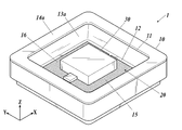
- 1 is a perspective view illustrating an electronic component mounting package according to an embodiment of the present disclosure.
- 1 is a perspective view illustrating an electronic component mounting package according to an embodiment of the present disclosure, showing a package on which electronic components have been mounted.
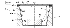
- 1 is a plan view schematically illustrating an electronic module according to an embodiment of the present disclosure. It is A1-A2 sectional view showing typically an electronic module concerning one embodiment of the present disclosure.
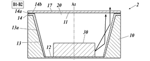
- 1 is a B1-B2 cross-sectional view schematically illustrating an electronic module according to an embodiment of the present disclosure.
- 1 is a schematic cross-sectional view for defining a direction on an inner peripheral surface of an electronic component mounting package according to an embodiment of the present disclosure.
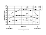
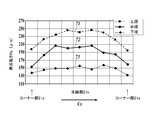
- FIG. 4 is a graph illustrating a film thickness distribution of a metal film according to an embodiment of the present disclosure.
- 4 is a graph illustrating a film thickness distribution of a metal film according to an embodiment of the present disclosure.
- 5 is a graph illustrating a distribution of surface roughness of a metal film according to an embodiment of the present disclosure.
- 5 is a graph illustrating a distribution of surface roughness of a metal film according to an embodiment of the present disclosure.
- FIG. 3 is a plan view illustrating a heat distribution of an adhesive sealing portion in the optical module according to an embodiment of the present disclosure.
- the optical element mounting package 1 of the present embodiment is mainly composed of a substrate 10 made of ceramic.
- the main surface (bottom and top) of the substrate 10 is a quadrilateral, and directions parallel to the sides are X and Y, and a direction perpendicular to the XY plane is Z, and triaxial orthogonal coordinates are described in the drawing.
- the substrate 10 has a cavity 20 that is open on the upper surface.
- the inner periphery 21 of the cavity 20 has a shape conforming to the outer shape of the substrate 10 and has a corner portion 21a and a straight portion 21b.
- four sides of the substrate 10 and four sides of the cavity 20 are arranged in parallel, and each corner has an R (roundness) with a predetermined curvature.
- the inner peripheral surface 13 of the cavity 20 is inclined outward from the bottom surface 12 toward the opening 11 of the cavity.
- the inner peripheral surface 13 of the cavity 20 is inclined so as to be closest to the bottom surface 12 and farthest to the opening 11 with respect to the center axis Az of the cavity 20 in the Z direction. Therefore, the area of the XY cross section of the cavity 20 is smallest at the bottom surface 12 and wide at the opening 11.
- a metal film 13 a is located on the inner peripheral surface 13 of the cavity 20. Further, the metal film 14a is also located on the upper end surface 14 of the substrate around the cavity 20. These metal films 13a and 14a are located, for example, continuously.
- As the metal film 13a for example, an aluminum film which is a metal having a high thermal conductivity and a high reflectance is applied, and has at least one metal film selected from a tungsten film, a nickel film, and a gold film in the inner layer. May be. Further, at least one metal film selected from a tungsten film, a nickel film, and a gold film is applied as the metal film 14a.
- Electrode patterns 15 and 16 are located on the bottom surface 12 of the cavity 20 to form an electronic component mounting portion.
- the electrodes of the optical element 30 are electrically and mechanically connected to the electrode patterns 15 and 16 and mounted.
- the electrode patterns 15 and 16 are electrically connected to external connection pads on the bottom surface of the substrate 10.
- a translucent lid 17 covering the opening 11 of the cavity 20 is joined to the substrate upper end surface 14 around the cavity 20 (via a metal film 14 a and an adhesive 14 b), and the lid 17 closes the cavity 20.
- the optical module 2 is provided.
- FIG. 4 shows a direction on the inner peripheral surface 13 of the cavity 20. That is, the circumferential direction of the inner peripheral surface 13 is Cz, and the direction from the opening 11 to the bottom surface 12 along the inner peripheral surface 13 is Dz.
- FIG. 5 shows a graph of the film thickness distribution of the metal film 13a in the Cz direction. An upper graph 51 near the opening 11, a lower graph 53 near the bottom surface 12, and a middle graph 52 between them are shown. The range shown is one side (from a corner to the next corner).
- FIG. 6 shows a graph of the thickness distribution of the metal film 13a in the Dz direction. A graph 61 of the thickness distribution in the Dz direction at the center of the straight portion 21b and a graph 62 of the thickness distribution in the Dz direction at the corner 21a are shown.
- the metal film 13a has a greater thickness in the straight portion 21b than in the corner portion 21a on the inner circumference at the same distance from the bottom surface 12.
- the upper graph 51 shows the thickness distribution in the Cz direction on the inner circumference at the same distance from the bottom surface 12.
- each of the middle graph 52 and the lower graph 53 shows the thickness distribution in the Cz direction on the inner circumference at the same distance from the bottom surface 12.
- the thickness of the metal film 13a is larger at the straight portion than at the corner.
- FIG. 6 it can be confirmed that the thickness of the metal film 13a is larger in the straight portion than in the corner portion.
- the thickness of the metal film 13a gradually decreases as the position approaches the bottom surface 12 from the opening 11 of the cavity 20 in each of the corner portion 21a and the straight portion 21b.
- the surface roughness of the metal film 13a is larger in the straight portion 21b than in the corner portion 21a.
- the surface roughness of the metal film 13a gradually decreases as approaching the bottom surface 12 from the opening 11 of the cavity 20.
- the thick embossed area 13b shown in FIGS. 3A and 3B is an area schematically showing a part of the metal film 13a that is thicker than its surroundings and has a rough surface.
- FIG. 9 shows a heat distribution of the adhesive sealing portion in the optical module 2 of the present embodiment.
- FIG. 9 is a graph showing the density of the heat distribution generated at the time of sealing the adhesive at the upper end surface (14) of the substrate around the cavity (20) by shading.
- the thickness of the metal film 13a in the corner portion 21a is relatively small, but as shown by the arrow in FIG.
- the heat path through which heat is absorbed and radiated is located, and the non-uniformity of the heat distribution of the sealing portion is reduced.
- the metal film 13a in the thick embossed region 13b has a large surface area due to the large surface roughness and is excellent in heat dissipation. As a result, the reliability of the sealing structure is improved.
- the optical characteristics are as follows.
- the optical element 30 is a light emitting element such as a light emitting diode
- the light emitted from the optical element 30 toward the inner peripheral surface 13 travels as shown by arrows in FIGS. 3B and 3C.
- FIG. 3B in the cross section A1-A2 crossing the straight portions 21b, 21b opposed to each other, the light is reflected by the metal film 13a in the thick embossed region 13b, and cannot be emitted outside through the opening 11 and the lid 17. Light that travels and is confined is produced. This is because the surface roughness of the metal film 13a in the thick embossed area 13b is large.
- the loss due to the light that cannot be emitted to the outside is called light confinement loss. Therefore, it can be said that light confinement loss is large in the vicinity of the linear portion 21b due to the surface of the thick embossed region 13b having a large surface roughness. As shown in FIG. 3C, in section B1-B2 crossing corner portions 21a facing each other, the thickness of metal film 13a is relatively small even near opening 11, and the surface roughness of metal film 13a is small. Therefore, the light confinement loss can be reduced. Therefore, the light emission efficiency of the optical module 2 can be improved. When the optical element is a light receiving element such as a photodiode, the light receiving efficiency of the optical module 2 can be improved.
- the light emission amount near the corner portion 21a far from the center of the optical element 30 as the light source is increased.
- the light emission amount can be made uniform over the entire light emitting surface of the optical module 2.
- the optical element is a light receiving element such as a photodiode, it is possible to make the amount of light received uniform over the entire light receiving surface of the optical module 2.
- the electronic component mounted on the electronic component mounting package is an optical element.
- the electronic component mounting package of the present disclosure is not limited to this, and any electronic component may be mounted. . In either case, the effect of improving the reliability of the sealing structure can be obtained.
- the above optical characteristics are for the case where the electronic component is an optical element.
- the present disclosure can be used for electronic component mounting packages and electronic modules.
Landscapes
- Led Device Packages (AREA)
Abstract
電子部品搭載用パッケージ及び電子モジュールは、セラミックを基材とし、底面に電子部品実装部が位置し、内周面に金属膜が施されたキャビティが形成された基板を備える。キャビティの内周は、コーナー部と直線部を有した形状に形成され、底面から同距離の内周において、金属膜がコーナー部より直線部において厚く、また表面粗さが粗く形成されており、金属膜のうち周囲より厚く、表面が粗い厚盛領域が直線部の上部に設けられる。
Description
本開示は、電子部品搭載用パッケージ及び電子モジュールに関する。
従来、セラミックを基材とし、底面に電子部品実装部が構成されたキャビティを形成し、当該電子部品実装部にLEDなどの発光素子を実装するようにした発光素子用セラミックパッケージが知られている(特開2006-41179号)。発光素子を収めるそのキャビティの内周面は、底面から開口に向かって外側に傾斜しており、発光素子から出射しキャビティの側面で反射した光が開口端から外部に出射し、高効率に光出射するように構成されている。キャビティの側面の反射率を向上するために当該側面に金属膜を施すことが行われる(特開2007-234846号)。
本開示の第一の態様は、セラミックを基材とし、底面に電子部品実装部が位置し、内周面に金属膜が位置したキャビティを有した基板を備え、前記キャビティの内周は、コーナー部と直線部を有しており、前記底面から同距離の内周において、前記金属膜が前記コーナー部より前記直線部において厚みが大きい電子部品搭載用パッケージである。
本開示の第二の態様は、セラミックを基材とし、底面に電子部品実装部が位置し、内周面に金属膜が位置したキャビティを有した基板を備え、前記キャビティの内周は、コーナー部と直線部を有しており、前記底面から同距離の内周において、前記金属膜の表面粗さが前記コーナー部より前記直線部において大きい電子部品搭載用パッケージである。
以下に本開示の一実施形態につき図面を参照して説明する。
本実施形態においては、電子部品搭載用パッケージに実装する電子部品を光学素子(発光ダイオード)とした光学モジュールの例につき説明する。
図1から図3A-Cに示すように本実施形態の光学素子搭載用パッケージ1は、セラミックを基材とした基板10を主体として構成される。基板10は、主面(底面及び上面)が四辺形であり、その辺々と平行な方向をX,Yとし、XY平面に垂直な方向をZとして3軸直交座標を図中に記載する。
図1から図3A-Cに示すように本実施形態の光学素子搭載用パッケージ1は、セラミックを基材とした基板10を主体として構成される。基板10は、主面(底面及び上面)が四辺形であり、その辺々と平行な方向をX,Yとし、XY平面に垂直な方向をZとして3軸直交座標を図中に記載する。
基板10には、上面に開口するキャビティ20が形成されている。Z方向視(図3A)においてキャビティ20の内周21は、基板10の外形に合せた形状であり、コーナー部21aと直線部21bを有している。Z方向視において、基板10の4辺と、キャビティ20の4辺とが平行に配置され、ぞれぞれの角は所定曲率のR(丸み)を有している。
キャビティ20の内周面13は底面12からキャビティの開口11に向かって外側に傾斜している。すなわち、キャビティ20のZ方向の中心軸Azに対して、キャビティ20の内周面13は、底面12で最も近く、開口11で最も離れるように傾斜している。したがって、キャビティ20のXY断面の面積は、底面12で最も小さく、開口11で広くなる。
キャビティ20の内周面13は底面12からキャビティの開口11に向かって外側に傾斜している。すなわち、キャビティ20のZ方向の中心軸Azに対して、キャビティ20の内周面13は、底面12で最も近く、開口11で最も離れるように傾斜している。したがって、キャビティ20のXY断面の面積は、底面12で最も小さく、開口11で広くなる。
キャビティ20の内周面13には、金属膜13aが位置している。さらにキャビティ20の周囲の基板上端面14にも金属膜14aが位置している。これらの金属膜13a,14aは、例えば連続して位置している。金属膜13aとしては、例えば、熱伝導率が大きく、反射率が高い金属であるアルミニウム膜が適用され、タングステン膜、ニッケル膜および金膜の中から選ばれる少なくとも1つの金属膜を内層に有していてもよい。また、金属膜14aとしては、タングステン膜、ニッケル膜および金膜の中から選ばれる少なくとも1つの金属膜が適用される。
キャビティ20の底面12には、電極パターン15,16が位置して電子部品実装部が構成されている。光学素子30の電極が電極パターン15,16に電気的及び機械的に接続されて実装される。電極パターン15,16は、基板10の底面の外部接続パッドに導通している。
キャビティ20の開口11を覆う透光性の蓋体17が、キャビティ20の周囲の基板上端面14に(金属膜14a、接着剤14bを介して)接合され、蓋体17がキャビティ20を塞いで光学モジュール2とされる。
キャビティ20の開口11を覆う透光性の蓋体17が、キャビティ20の周囲の基板上端面14に(金属膜14a、接着剤14bを介して)接合され、蓋体17がキャビティ20を塞いで光学モジュール2とされる。
次に、金属膜13aの膜厚と表面粗さの分布につき説明する。
図4に示すように、キャビティ20の内周面13上における方向を定義する。すなわち、内周面13の周方向をCzとし、内周面13に沿って開口11から底面12への方向をDzとする。
図5にCz方向の金属膜13aの膜厚分布のグラフを示す。開口11に近い上段のグラフ51、底面12に近い下段のグラフ53と、その中間の中段のグラフ52をそれぞれ示した。示される範囲としては1辺分(コーナー部から次のコーナー部まで)である。図6にDz方向の金属膜13aの厚み分布のグラフが示す。直線部21b中央におけるDz方向の膜厚分布のグラフ61と、コーナー部21aにおけるDz方向の膜厚分布のグラフ62とを示す。
図4に示すように、キャビティ20の内周面13上における方向を定義する。すなわち、内周面13の周方向をCzとし、内周面13に沿って開口11から底面12への方向をDzとする。
図5にCz方向の金属膜13aの膜厚分布のグラフを示す。開口11に近い上段のグラフ51、底面12に近い下段のグラフ53と、その中間の中段のグラフ52をそれぞれ示した。示される範囲としては1辺分(コーナー部から次のコーナー部まで)である。図6にDz方向の金属膜13aの厚み分布のグラフが示す。直線部21b中央におけるDz方向の膜厚分布のグラフ61と、コーナー部21aにおけるDz方向の膜厚分布のグラフ62とを示す。
図5、図6に示すように、底面12から同距離の内周において、金属膜13aがコーナー部21aより直線部21bにおいて厚みが大きい。図5に示すように、上段のグラフ51は、底面12から同距離の内周におけるCz方向の厚み分布を示す。同様に中段のグラフ52及び下段のグラフ53のそれぞれも、底面12から同距離の内周におけるCz方向の厚み分布を示す。これらのいずれのグラフを参照してもわかるように、金属膜13aがコーナー部より直線部において厚みが大きい。また、図6を参照しても、金属膜13aがコーナー部より直線部において厚みが大きいことが確認できる。
また、図6に示すようにコーナー部21a及び直線部21bのそれぞれにおいてキャビティ20の開口11から底面12に近づくほど、金属膜13aの厚みが次第に小さい。
図7に示すように底面12から同距離の内周において、金属膜13aの表面粗さがコーナー部21aより直線部21bにおいて大きい。
また、図8に示すようにコーナー部21a及び直線部21bのそれぞれにおいてキャビティ20の開口11から底面12に近づくほど、金属膜13aの表面粗さが次第に小さい。
以上説明したことから、図3A,Bに示す厚盛領域13bは、金属膜13aのうち周囲より厚く、表面が粗い部分を模式的に示した領域である。
また、図8に示すようにコーナー部21a及び直線部21bのそれぞれにおいてキャビティ20の開口11から底面12に近づくほど、金属膜13aの表面粗さが次第に小さい。
以上説明したことから、図3A,Bに示す厚盛領域13bは、金属膜13aのうち周囲より厚く、表面が粗い部分を模式的に示した領域である。
次に、以上説明した構成による作用効果につき説明する。
図9に本実施形態の光学モジュール2における接着封止部の熱分布を示す。図9は、キャビティ(20)の周囲の基板上端面(14)における接着剤封止時に生じる熱分布の高低を濃淡で表現したものである。
本実施形態の光学モジュール2にあっては、コーナー部21aの金属膜13aの厚みは比較的小さいが、図9中に矢印で示すように、比較的容量の大きい厚盛領域13bの金属膜13aに吸熱され、放熱される熱経路が位置し、封止部の熱分布の不均一性が緩和される。厚盛領域13bの金属膜13aは、表面粗さが大きい分表面積が大きく放熱性に優れる。その結果、封止構造の信頼性が向上する。
図9に本実施形態の光学モジュール2における接着封止部の熱分布を示す。図9は、キャビティ(20)の周囲の基板上端面(14)における接着剤封止時に生じる熱分布の高低を濃淡で表現したものである。
本実施形態の光学モジュール2にあっては、コーナー部21aの金属膜13aの厚みは比較的小さいが、図9中に矢印で示すように、比較的容量の大きい厚盛領域13bの金属膜13aに吸熱され、放熱される熱経路が位置し、封止部の熱分布の不均一性が緩和される。厚盛領域13bの金属膜13aは、表面粗さが大きい分表面積が大きく放熱性に優れる。その結果、封止構造の信頼性が向上する。
また、光学特性については次の通りである。
光学素子30が発光ダイオード等の発光素子である場合、光学素子30から内周面13方向へ出射した光は、図3B,C中に矢印で示すように進行する。
図3Bに示すように互いに対向する直線部21b,21bを横断する断面A1-A2においては、厚盛領域13bの金属膜13aで反射して、開口11及び蓋体17を通して外部に出射できない方向に進行し閉じ込められる光が生じる。厚盛領域13bの金属膜13aの表面粗さが大きいためである。光学素子30が発光した光のうち、外部に出射できない光による損失分を、光閉じ込めロスと呼ぶ。したがって、表面粗さが大きい厚盛領域13bの表面によって、直線部21b近傍では光閉じ込めロスが大きいということができる。
図3Cに示すように互いに対向するコーナー部21a,21aを横断する断面B1-B2においては、金属膜13aの厚みは開口11近傍であっても比較的小さく、金属膜13aの表面粗さが小さいため、光閉じ込めロスが小さく抑えられる。
したがって、光学モジュール2の光出射効率を向上することができる。
光学素子をフォトダイオード等の受光素子とした場合には、光学モジュール2の受光効率を向上することができる。
また、光源である光学素子30の中心に近い直線部21b近傍での光出射量を抑える一方で、光源である光学素子30の中心から遠いコーナー部21a近傍での光出射量を上げることで、光学モジュール2の発光面全域における発光量の均一化を図ることができる。
光学素子をフォトダイオード等の受光素子とした場合には、光学モジュール2の受光面全域における受光量の均一化を図ることができる。
光学素子30が発光ダイオード等の発光素子である場合、光学素子30から内周面13方向へ出射した光は、図3B,C中に矢印で示すように進行する。
図3Bに示すように互いに対向する直線部21b,21bを横断する断面A1-A2においては、厚盛領域13bの金属膜13aで反射して、開口11及び蓋体17を通して外部に出射できない方向に進行し閉じ込められる光が生じる。厚盛領域13bの金属膜13aの表面粗さが大きいためである。光学素子30が発光した光のうち、外部に出射できない光による損失分を、光閉じ込めロスと呼ぶ。したがって、表面粗さが大きい厚盛領域13bの表面によって、直線部21b近傍では光閉じ込めロスが大きいということができる。
図3Cに示すように互いに対向するコーナー部21a,21aを横断する断面B1-B2においては、金属膜13aの厚みは開口11近傍であっても比較的小さく、金属膜13aの表面粗さが小さいため、光閉じ込めロスが小さく抑えられる。
したがって、光学モジュール2の光出射効率を向上することができる。
光学素子をフォトダイオード等の受光素子とした場合には、光学モジュール2の受光効率を向上することができる。
また、光源である光学素子30の中心に近い直線部21b近傍での光出射量を抑える一方で、光源である光学素子30の中心から遠いコーナー部21a近傍での光出射量を上げることで、光学モジュール2の発光面全域における発光量の均一化を図ることができる。
光学素子をフォトダイオード等の受光素子とした場合には、光学モジュール2の受光面全域における受光量の均一化を図ることができる。
以上説明した実施形態においては、電子部品搭載用パッケージに実装する電子部品を光学素子としたが、本開示の電子部品搭載用パッケージはこれに限らず、どのような電子部品を搭載してもよい。いずれの場合も封止構造の信頼性向上の効果が得られる。但し、上記の光学特性については、電子部品を光学素子とした場合である。
本開示は、電子部品搭載用パッケージ及び電子モジュールに利用することができる。
Claims (9)
- セラミックを基材とし、底面に電子部品実装部が位置し、内周面に金属膜が位置したキャビティを有した基板を備え、
前記キャビティの内周は、コーナー部と直線部を有しており、
前記底面から同距離の内周において、前記金属膜が前記コーナー部より前記直線部において厚みが大きい電子部品搭載用パッケージ。 - 前記底面から同距離の内周において、前記金属膜の表面粗さが前記コーナー部より前記直線部において大きい請求項1に記載の電子部品搭載用パッケージ。
- セラミックを基材とし、底面に電子部品実装部が位置し、内周面に金属膜が位置したキャビティを有した基板を備え、
前記キャビティの内周は、コーナー部と直線部を有しており、
前記底面から同距離の内周において、前記金属膜の表面粗さが前記コーナー部より前記直線部において大きい電子部品搭載用パッケージ。 - 前記コーナー部及び前記直線部のそれぞれにおいて前記キャビティの開口から底面に近づくほど、前記金属膜の厚みが次第に小さい請求項1から請求項3のうちいずれか一に記載の電子部品搭載用パッケージ。
- 前記コーナー部及び前記直線部のそれぞれにおいて前記キャビティの開口端から底面に近づくほど、前記金属膜の表面粗さが次第に小さい請求項1から請求項4のうちいずれか一に記載の電子部品搭載用パッケージ。
- 前記内周面に隣接する前記キャビティの周囲の端面に金属膜が位置し、当該端面上の金属膜と、前記内周面上の金属膜とが連続して位置している請求項1から請求項5のうちいずれか一に記載の電子部品搭載用パッケージ。
- 前記内周面は前記底面から前記キャビティの開口に向かって外側に傾斜している請求項1から請求項6のうちいずれか一に記載の電子部品搭載用パッケージ。
- 請求項1から請求項7のうちいずれか一に記載の電子部品搭載用パッケージが適用された電子モジュールであって、
前記電子部品実装部に電子部品が実装され、前記キャビティの開口を覆う蓋体が、前記キャビティの周囲の端面に接合され、前記蓋体が前記キャビティを塞いだ電子モジュール。 - 請求項7に記載の電子部品搭載用パッケージが適用された電子モジュールであって、
前記電子部品実装部に光学素子が実装され、前記キャビティの開口を覆う透光性の蓋体が、前記キャビティの周囲の端面に接合され、前記蓋体が前記キャビティを塞いだ電子モジュール。
Priority Applications (3)
| Application Number | Priority Date | Filing Date | Title |
|---|---|---|---|
| US17/256,038 US11876152B2 (en) | 2018-06-29 | 2019-06-28 | Electronic component mounting package and electronic module |
| CN201980042914.5A CN112368823B (zh) | 2018-06-29 | 2019-06-28 | 电子部件搭载用封装件以及电子模块 |
| JP2020527673A JP7117379B2 (ja) | 2018-06-29 | 2019-06-28 | 電子部品搭載用パッケージ及び電子モジュール |
Applications Claiming Priority (2)
| Application Number | Priority Date | Filing Date | Title |
|---|---|---|---|
| JP2018124327 | 2018-06-29 | ||
| JP2018-124327 | 2018-06-29 |
Publications (1)
| Publication Number | Publication Date |
|---|---|
| WO2020004606A1 true WO2020004606A1 (ja) | 2020-01-02 |
Family
ID=68986666
Family Applications (1)
| Application Number | Title | Priority Date | Filing Date |
|---|---|---|---|
| PCT/JP2019/025765 Ceased WO2020004606A1 (ja) | 2018-06-29 | 2019-06-28 | 電子部品搭載用パッケージ及び電子モジュール |
Country Status (4)
| Country | Link |
|---|---|
| US (1) | US11876152B2 (ja) |
| JP (1) | JP7117379B2 (ja) |
| CN (1) | CN112368823B (ja) |
| WO (1) | WO2020004606A1 (ja) |
Citations (3)
| Publication number | Priority date | Publication date | Assignee | Title |
|---|---|---|---|---|
| JP2003282955A (ja) * | 2001-07-19 | 2003-10-03 | Rohm Co Ltd | 反射ケース付半導体発光装置 |
| JP2005191111A (ja) * | 2003-12-24 | 2005-07-14 | Kyocera Corp | 発光素子収納用パッケージおよび発光装置 |
| JP2018037583A (ja) * | 2016-09-01 | 2018-03-08 | 日機装株式会社 | 光半導体装置および光半導体装置の製造方法 |
Family Cites Families (15)
| Publication number | Priority date | Publication date | Assignee | Title |
|---|---|---|---|---|
| JPH05235113A (ja) * | 1992-02-21 | 1993-09-10 | Toshiba Corp | 半導体装置 |
| JP2001147156A (ja) * | 1999-11-19 | 2001-05-29 | Murata Mfg Co Ltd | 赤外線センサ用熱吸収体およびその形成方法 |
| JP3929851B2 (ja) * | 2002-08-08 | 2007-06-13 | 三菱化学産資株式会社 | 床暖房用放熱板ブロック、および床暖房用放熱板ブロックの敷設方法 |
| JP4070195B2 (ja) * | 2002-11-27 | 2008-04-02 | 京セラ株式会社 | 発光素子収納用パッケージ |
| JP4038199B2 (ja) | 2004-07-27 | 2008-01-23 | 日本特殊陶業株式会社 | Led用セラミックパッケージ及びその製造方法 |
| US7700885B2 (en) * | 2005-04-25 | 2010-04-20 | Ngk Spark Plug Co., Ltd. | Wiring board |
| US20100002455A1 (en) * | 2005-11-24 | 2010-01-07 | Yoichi Matsuoka | Electronic Component Mounting Board and Method for Manufacturing Such Board |
| US7928462B2 (en) * | 2006-02-16 | 2011-04-19 | Lg Electronics Inc. | Light emitting device having vertical structure, package thereof and method for manufacturing the same |
| JP2007234846A (ja) | 2006-03-01 | 2007-09-13 | Ngk Spark Plug Co Ltd | 発光素子用セラミックパッケージ |
| JP2007305785A (ja) * | 2006-05-11 | 2007-11-22 | Nichia Chem Ind Ltd | 発光装置 |
| DE102009042479A1 (de) * | 2009-09-24 | 2011-03-31 | Msg Lithoglas Ag | Verfahren zum Herstellen einer Anordnung mit einem Bauelement auf einem Trägersubstrat und Anordnung sowie Verfahren zum Herstellen eines Halbzeuges und Halbzeug |
| KR20120027737A (ko) * | 2010-09-13 | 2012-03-22 | 현대모비스 주식회사 | 외장 앰프용 히트 싱크 |
| CN102969438A (zh) * | 2012-12-21 | 2013-03-13 | 左洪波 | Led用蓝宝石支架 |
| US9935251B1 (en) * | 2013-03-15 | 2018-04-03 | Hutchinson Technology Incorporated | LED chip packaging with high performance thermal dissipation |
| US9520281B2 (en) * | 2013-03-18 | 2016-12-13 | Epistar Corporation | Method of fabricating an optoelectronic device with a hollow component in epitaxial layer |
-
2019
- 2019-06-28 US US17/256,038 patent/US11876152B2/en active Active
- 2019-06-28 WO PCT/JP2019/025765 patent/WO2020004606A1/ja not_active Ceased
- 2019-06-28 JP JP2020527673A patent/JP7117379B2/ja active Active
- 2019-06-28 CN CN201980042914.5A patent/CN112368823B/zh active Active
Patent Citations (3)
| Publication number | Priority date | Publication date | Assignee | Title |
|---|---|---|---|---|
| JP2003282955A (ja) * | 2001-07-19 | 2003-10-03 | Rohm Co Ltd | 反射ケース付半導体発光装置 |
| JP2005191111A (ja) * | 2003-12-24 | 2005-07-14 | Kyocera Corp | 発光素子収納用パッケージおよび発光装置 |
| JP2018037583A (ja) * | 2016-09-01 | 2018-03-08 | 日機装株式会社 | 光半導体装置および光半導体装置の製造方法 |
Also Published As
| Publication number | Publication date |
|---|---|
| US20210151636A1 (en) | 2021-05-20 |
| US11876152B2 (en) | 2024-01-16 |
| CN112368823B (zh) | 2024-12-03 |
| JP7117379B2 (ja) | 2022-08-12 |
| CN112368823A (zh) | 2021-02-12 |
| JPWO2020004606A1 (ja) | 2021-07-08 |
Similar Documents
| Publication | Publication Date | Title |
|---|---|---|
| CN109404746B (zh) | 发光装置 | |
| JP5902823B2 (ja) | 発光素子パッケージ及びそれを備えるバックライトユニット | |
| KR20070042710A (ko) | 엘이디 패키지 | |
| CN102959746A (zh) | 光电子半导体构件 | |
| TWI899085B (zh) | 光學裝置 | |
| US8648360B2 (en) | Light-emitting diode structure | |
| JP2010103294A (ja) | 発光ダイオード | |
| JP6439776B2 (ja) | 発光装置 | |
| JP7117379B2 (ja) | 電子部品搭載用パッケージ及び電子モジュール | |
| JP6458825B2 (ja) | 光源装置 | |
| JP3915196B2 (ja) | 半導体発光装置 | |
| JP7174230B2 (ja) | 光源装置 | |
| JP2024111284A (ja) | 電子装置 | |
| JP7277844B2 (ja) | 発光装置 | |
| KR20190084807A (ko) | 발광 장치 | |
| KR20180105012A (ko) | 자동차 외장용 발광다이오드 패키지 | |
| JP6543391B2 (ja) | 半導体装置 | |
| TW201904093A (zh) | 發光二極體封裝結構及其製作方法、平面光源模組 | |
| JP2019140385A (ja) | 発光ダイオードのパッケージング構造 | |
| JP2020127056A (ja) | 発光装置 | |
| JP7506341B2 (ja) | 発光装置 | |
| JP2020188183A (ja) | 発光装置 | |
| US10082271B2 (en) | Laser light optical module utilizing reflective films for improved efficiency | |
| KR101294488B1 (ko) | 발광장치 | |
| JPWO2024058087A5 (ja) |
Legal Events
| Date | Code | Title | Description |
|---|---|---|---|
| 121 | Ep: the epo has been informed by wipo that ep was designated in this application |
Ref document number: 19825784 Country of ref document: EP Kind code of ref document: A1 |
|
| ENP | Entry into the national phase |
Ref document number: 2020527673 Country of ref document: JP Kind code of ref document: A |
|
| NENP | Non-entry into the national phase |
Ref country code: DE |
|
| 122 | Ep: pct application non-entry in european phase |
Ref document number: 19825784 Country of ref document: EP Kind code of ref document: A1 |