WO2020003725A1 - ピラー形成用導電ペースト - Google Patents
ピラー形成用導電ペースト Download PDFInfo
- Publication number
- WO2020003725A1 WO2020003725A1 PCT/JP2019/017602 JP2019017602W WO2020003725A1 WO 2020003725 A1 WO2020003725 A1 WO 2020003725A1 JP 2019017602 W JP2019017602 W JP 2019017602W WO 2020003725 A1 WO2020003725 A1 WO 2020003725A1
- Authority
- WO
- WIPO (PCT)
- Prior art keywords
- conductive paste
- acid
- copper
- fine particles
- pillar
- Prior art date
- Legal status (The legal status is an assumption and is not a legal conclusion. Google has not performed a legal analysis and makes no representation as to the accuracy of the status listed.)
- Ceased
Links
Images

Classifications
-
- H—ELECTRICITY
- H01—ELECTRIC ELEMENTS
- H01B—CABLES; CONDUCTORS; INSULATORS; SELECTION OF MATERIALS FOR THEIR CONDUCTIVE, INSULATING OR DIELECTRIC PROPERTIES
- H01B1/00—Conductors or conductive bodies characterised by the conductive materials; Selection of materials as conductors
- H01B1/20—Conductive material dispersed in non-conductive organic material
- H01B1/22—Conductive material dispersed in non-conductive organic material the conductive material comprising metals or alloys
-
- H—ELECTRICITY
- H10—SEMICONDUCTOR DEVICES; ELECTRIC SOLID-STATE DEVICES NOT OTHERWISE PROVIDED FOR
- H10W—GENERIC PACKAGES, INTERCONNECTIONS, CONNECTORS OR OTHER CONSTRUCTIONAL DETAILS OF DEVICES COVERED BY CLASS H10
- H10W70/00—Package substrates; Interposers; Redistribution layers [RDL]
- H10W70/20—Conductive package substrates serving as an interconnection, e.g. metal plates
- H10W70/24—Conductive package substrates serving as an interconnection, e.g. metal plates characterised by materials
-
- B—PERFORMING OPERATIONS; TRANSPORTING
- B22—CASTING; POWDER METALLURGY
- B22F—WORKING METALLIC POWDER; MANUFACTURE OF ARTICLES FROM METALLIC POWDER; MAKING METALLIC POWDER; APPARATUS OR DEVICES SPECIALLY ADAPTED FOR METALLIC POWDER
- B22F1/00—Metallic powder; Treatment of metallic powder, e.g. to facilitate working or to improve properties
- B22F1/05—Metallic powder characterised by the size or surface area of the particles
- B22F1/054—Nanosized particles
- B22F1/0545—Dispersions or suspensions of nanosized particles
-
- B—PERFORMING OPERATIONS; TRANSPORTING
- B22—CASTING; POWDER METALLURGY
- B22F—WORKING METALLIC POWDER; MANUFACTURE OF ARTICLES FROM METALLIC POWDER; MAKING METALLIC POWDER; APPARATUS OR DEVICES SPECIALLY ADAPTED FOR METALLIC POWDER
- B22F1/00—Metallic powder; Treatment of metallic powder, e.g. to facilitate working or to improve properties
- B22F1/10—Metallic powder containing lubricating or binding agents; Metallic powder containing organic material
- B22F1/102—Metallic powder coated with organic material
-
- B—PERFORMING OPERATIONS; TRANSPORTING
- B22—CASTING; POWDER METALLURGY
- B22F—WORKING METALLIC POWDER; MANUFACTURE OF ARTICLES FROM METALLIC POWDER; MAKING METALLIC POWDER; APPARATUS OR DEVICES SPECIALLY ADAPTED FOR METALLIC POWDER
- B22F1/00—Metallic powder; Treatment of metallic powder, e.g. to facilitate working or to improve properties
- B22F1/10—Metallic powder containing lubricating or binding agents; Metallic powder containing organic material
- B22F1/107—Metallic powder containing lubricating or binding agents; Metallic powder containing organic material containing organic material comprising solvents, e.g. for slip casting
-
- B—PERFORMING OPERATIONS; TRANSPORTING
- B22—CASTING; POWDER METALLURGY
- B22F—WORKING METALLIC POWDER; MANUFACTURE OF ARTICLES FROM METALLIC POWDER; MAKING METALLIC POWDER; APPARATUS OR DEVICES SPECIALLY ADAPTED FOR METALLIC POWDER
- B22F9/00—Making metallic powder or suspensions thereof
- B22F9/16—Making metallic powder or suspensions thereof using chemical processes
- B22F9/18—Making metallic powder or suspensions thereof using chemical processes with reduction of metal compounds
- B22F9/24—Making metallic powder or suspensions thereof using chemical processes with reduction of metal compounds starting from liquid metal compounds, e.g. solutions
-
- H—ELECTRICITY
- H10—SEMICONDUCTOR DEVICES; ELECTRIC SOLID-STATE DEVICES NOT OTHERWISE PROVIDED FOR
- H10W—GENERIC PACKAGES, INTERCONNECTIONS, CONNECTORS OR OTHER CONSTRUCTIONAL DETAILS OF DEVICES COVERED BY CLASS H10
- H10W72/00—Interconnections or connectors in packages
- H10W72/20—Bump connectors, e.g. solder bumps or copper pillars; Dummy bumps; Thermal bumps
-
- B—PERFORMING OPERATIONS; TRANSPORTING
- B22—CASTING; POWDER METALLURGY
- B22F—WORKING METALLIC POWDER; MANUFACTURE OF ARTICLES FROM METALLIC POWDER; MAKING METALLIC POWDER; APPARATUS OR DEVICES SPECIALLY ADAPTED FOR METALLIC POWDER
- B22F1/00—Metallic powder; Treatment of metallic powder, e.g. to facilitate working or to improve properties
- B22F1/17—Metallic particles coated with metal
-
- B—PERFORMING OPERATIONS; TRANSPORTING
- B22—CASTING; POWDER METALLURGY
- B22F—WORKING METALLIC POWDER; MANUFACTURE OF ARTICLES FROM METALLIC POWDER; MAKING METALLIC POWDER; APPARATUS OR DEVICES SPECIALLY ADAPTED FOR METALLIC POWDER
- B22F2304/00—Physical aspects of the powder
- B22F2304/05—Submicron size particles
-
- B—PERFORMING OPERATIONS; TRANSPORTING
- B22—CASTING; POWDER METALLURGY
- B22F—WORKING METALLIC POWDER; MANUFACTURE OF ARTICLES FROM METALLIC POWDER; MAKING METALLIC POWDER; APPARATUS OR DEVICES SPECIALLY ADAPTED FOR METALLIC POWDER
- B22F2999/00—Aspects linked to processes or compositions used in powder metallurgy
-
- H—ELECTRICITY
- H10—SEMICONDUCTOR DEVICES; ELECTRIC SOLID-STATE DEVICES NOT OTHERWISE PROVIDED FOR
- H10W—GENERIC PACKAGES, INTERCONNECTIONS, CONNECTORS OR OTHER CONSTRUCTIONAL DETAILS OF DEVICES COVERED BY CLASS H10
- H10W72/00—Interconnections or connectors in packages
- H10W72/01—Manufacture or treatment
- H10W72/012—Manufacture or treatment of bump connectors, dummy bumps or thermal bumps
- H10W72/01221—Manufacture or treatment of bump connectors, dummy bumps or thermal bumps using local deposition
- H10W72/01223—Manufacture or treatment of bump connectors, dummy bumps or thermal bumps using local deposition in liquid form, e.g. by dispensing droplets or by screen printing
-
- H—ELECTRICITY
- H10—SEMICONDUCTOR DEVICES; ELECTRIC SOLID-STATE DEVICES NOT OTHERWISE PROVIDED FOR
- H10W—GENERIC PACKAGES, INTERCONNECTIONS, CONNECTORS OR OTHER CONSTRUCTIONAL DETAILS OF DEVICES COVERED BY CLASS H10
- H10W72/00—Interconnections or connectors in packages
- H10W72/01—Manufacture or treatment
- H10W72/012—Manufacture or treatment of bump connectors, dummy bumps or thermal bumps
- H10W72/01251—Changing the shapes of bumps
- H10W72/01255—Changing the shapes of bumps by using masks
-
- H—ELECTRICITY
- H10—SEMICONDUCTOR DEVICES; ELECTRIC SOLID-STATE DEVICES NOT OTHERWISE PROVIDED FOR
- H10W—GENERIC PACKAGES, INTERCONNECTIONS, CONNECTORS OR OTHER CONSTRUCTIONAL DETAILS OF DEVICES COVERED BY CLASS H10
- H10W72/00—Interconnections or connectors in packages
- H10W72/01—Manufacture or treatment
- H10W72/012—Manufacture or treatment of bump connectors, dummy bumps or thermal bumps
- H10W72/01261—Chemical or physical modification, e.g. by sintering or anodisation
-
- H—ELECTRICITY
- H10—SEMICONDUCTOR DEVICES; ELECTRIC SOLID-STATE DEVICES NOT OTHERWISE PROVIDED FOR
- H10W—GENERIC PACKAGES, INTERCONNECTIONS, CONNECTORS OR OTHER CONSTRUCTIONAL DETAILS OF DEVICES COVERED BY CLASS H10
- H10W72/00—Interconnections or connectors in packages
- H10W72/20—Bump connectors, e.g. solder bumps or copper pillars; Dummy bumps; Thermal bumps
- H10W72/221—Structures or relative sizes
- H10W72/225—Bumps having a filler embedded in a matrix
-
- H—ELECTRICITY
- H10—SEMICONDUCTOR DEVICES; ELECTRIC SOLID-STATE DEVICES NOT OTHERWISE PROVIDED FOR
- H10W—GENERIC PACKAGES, INTERCONNECTIONS, CONNECTORS OR OTHER CONSTRUCTIONAL DETAILS OF DEVICES COVERED BY CLASS H10
- H10W72/00—Interconnections or connectors in packages
- H10W72/20—Bump connectors, e.g. solder bumps or copper pillars; Dummy bumps; Thermal bumps
- H10W72/251—Materials
- H10W72/252—Materials comprising solid metals or solid metalloids, e.g. PbSn, Ag or Cu
-
- H—ELECTRICITY
- H10—SEMICONDUCTOR DEVICES; ELECTRIC SOLID-STATE DEVICES NOT OTHERWISE PROVIDED FOR
- H10W—GENERIC PACKAGES, INTERCONNECTIONS, CONNECTORS OR OTHER CONSTRUCTIONAL DETAILS OF DEVICES COVERED BY CLASS H10
- H10W72/00—Interconnections or connectors in packages
- H10W72/20—Bump connectors, e.g. solder bumps or copper pillars; Dummy bumps; Thermal bumps
- H10W72/251—Materials
- H10W72/253—Materials not comprising solid metals or solid metalloids, e.g. polymers or ceramics
Definitions
- the present invention relates to a conductive paste containing metal fine particles for a metal pillar (Pillar) or a metal post (Post), which is a terminal for flip chip mounting, which is a connection method between a semiconductor chip and a package interposer, in a semiconductor package.
- an electronic circuit is formed on a semiconductor chip, and an electrode on the semiconductor chip is connected to an electrode on a semiconductor package.
- electrodes on a semiconductor chip and electrodes on a semiconductor package have been electrically connected using a bonding wire made of gold or copper.
- a flip chip method is used as an electrical connection method between a semiconductor chip and a semiconductor package.
- a gold bump or a solder bump is used as a typical connection method in the flip chip method.
- flip chip technology using copper pillars has recently attracted attention.
- the copper pillar is formed on a semiconductor chip, and a tip of the copper pillar is connected to an electrode of a semiconductor package.
- Copper pillars having a pillar diameter of 70 ⁇ m or less and a pillar height of 50 to 60 ⁇ m are generally used. Since the copper pillar is made of copper having a low electric resistance, the copper pillar can cope with a large current as compared with the solder bump. In addition, the copper pillar can reduce the amount of supplied solder as compared with the solder bump, so that the bump pitch can be reduced. Furthermore, while gold bumps have a small contact area with electrodes, copper pillars can handle large currents because they can maintain the same cross-sectional area from the electrodes on the semiconductor chip to the electrodes on the semiconductor package. Has advantages. For the above reasons, the production of copper pillars is important in semiconductor mounting, and a method for easily producing copper pillars is desired.
- a method of forming a copper pillar on a substrate a method using a plating technique is known.
- a plating layer called a seed layer is formed on an electrode pad, and copper pillars are formed by electrolytic plating.
- a step of removing the patterned resist layer and seed layer after manufacturing the pillars is required because a seed layer is provided on the entire surface.
- the step of removing the seed layer by etching there is a problem that it is difficult to form fine pillars by plating using an undercut.
- a method of forming a copper pillar by a plating technique there is a method of using electroless plating.
- a method of forming a photoresist layer on a semiconductor chip, opening a photoresist layer at a portion where a copper pillar is to be formed, forming copper plating in an electroless portion at the opening portion, and further forming a solder plating on a top portion of the copper plating. is there.
- this method in order to form an elongated copper pillar having a large height / diameter ratio (aspect ratio) of the copper pillar, it is necessary to grow plating in a deep hole having a small diameter. In this case, it is difficult to continuously supply a plating solution having a sufficient concentration to the opening, and the growth of the plating is slowed and the throughput is deteriorated. There is a problem that quality and reproducibility are problematic due to the occurrence of voids in the copper to be produced.
- the plating method requires a large amount of waste liquid to be regenerated or disposed of, and has a large environmental load and requires high costs for equipment maintenance, so alternative means are desired.
- An object of the present invention is to provide a metal pillar having the same shape with good reproducibility while preventing undercut by producing a pillar by an embedding method using the pillar-forming conductive paste of the present invention.
- a conductive paste which is fine metal fine particles and is characterized by a specific metal fine particle content is particularly notable in forming pillars. was found to be effective.
- the present invention is a conductive paste for forming a pillar, comprising metal fine particles and a protective agent, wherein the metal fine particles have a particle diameter of less than 1 ⁇ m, and the content of the metal fine particles in the conductive paste is less than 1 ⁇ m. It is a conductive paste for forming pillars, which has a concentration of 40 to less than 95% by mass.
- the present invention is a conductive paste for producing a pillar by a filling method.
- a pillar can be easily formed by filling a conductive paste in an opening portion of a patterned resist layer with a squeegee or the like without using a plating technique which is a conventional technique.
- the undercut at the time of etching which has been a problem of the conventional method, can be solved, and fine copper pillars can be formed. Pillar fabrication using a conductive paste is not subject to restrictions such as deterioration of the plating solution or the rate of diffusion of ions, and thus it is considered that the problems of the quality and reproducibility of the electroless plating method may be solved.
- the metal species that can be used as the metal fine particles of the present invention is not particularly limited as long as the metal species can chemically bond to a functional group in a protective agent described later.
- gold, silver, copper, nickel, zinc, aluminum, platinum, palladium, tin, chromium, lead, tungsten, and the like can be used.
- the metal species may be one kind, a mixture of two or more kinds, or an alloy.
- the content of the metal fine particles in the conductive paste can be used in a range of 40 to less than 95% by mass. More preferably, it can be used in a concentration range of 60 to 90% by mass.
- a compound having a functional group having an affinity for metal fine particles or a solvent can be arbitrarily selected.
- the protective agent used can be used regardless of the molecular weight.
- a protective agent having a carboxy group, a phosphoric acid group, a sulfonic acid group, a heteroaromatic group (for example, an imidazole group) or the like having a rather strong adsorption capacity for metal high dispersion stability to fine particles can be obtained.
- Sex can be added.
- amino groups eg, dimethylaminoethyl group, dimethylaminopropyl group
- hydroxy groups hydroxyethyl group, hydroxypropyl group
- the protective agent concentration in the conductive paste can be used within a range of 15% by mass or less in the entire paste. More preferably, it is in the range of 10% by mass or less. If the concentration of the protective agent is too high, a necking phenomenon between metal particles does not sufficiently occur during sintering, and it becomes difficult to develop high conductivity.
- carboxylic acids having a carboxyl group include formic acid, acetic acid, propionic acid, butyric acid, valeric acid, caproic acid, enanthic acid, caprylic acid, pelargonic acid, capric acid, lauric acid, myristic acid, palmitic acid, margaric acid, Stearic acid, behenic acid, oleic acid, palmitooleic acid, eicosenoic acid, erucic acid, nervonic acid, ricinoleic acid, oxalic acid, malonic acid, succinic acid, glutaric acid, adipic acid, pimelic acid, suberic acid, azelaic acid, Sebacic acid, diglycolic acid, maleic acid, itaconic acid, benzoic acid, N-oleyl sarcosine, N-carbobenzoxy-4-aminobutyric acid,
- amines having an amino group include 2-methoxyethylamine, 2-ethoxyethylamine, 2-isopropoxyethylamine, 3-methoxypropylamine, 3-ethoxypropylamine, 3-isopropoxypropylamine, 3- (2- Ethylhexyloxy) propylamine, N-methylethylenediamine, N-ethylethylenediamine, N-isopropylethylenediamine, N-methyl-1,3-propanediamine, 3-isopropylaminopropylamine, N, N-dimethylethylenediamine, N, N- Diethylethylenediamine, N, N-dimethyl-1,3-propanediamine, N, N-diethyl-1,3-propanediamine, N- (3-aminopropyl) morpholine, N- (tert-butoxycarbonyl) -1, -Diaminobutane, N- (tert-butoxycarbonyl)
- an organic compound having a polyethylene oxide structure having 8 to 200 carbon atoms can be used.
- the polyethylene oxide portion of the protective agent has excellent affinity with the specific solvent used in the present invention such as an alcoholic solvent having a boiling point of 250 ° C. or lower, so that aggregation of metal fine particles can be strongly suppressed and high dispersion of metal fine particles can be achieved. Make it possible. In other words, since the metal fine particles are in a state of being densely packed, a high-density packing is possible without generating a void due to the decomposition and removal of the protective agent and the solvent by the heat treatment.
- the metal fine particles synthesized using the protective agent of the present invention have a small amount of the protective agent as low as about 2 to 10% by mass and do not prevent the necking phenomenon of the metal particles during firing.
- metal fine particles composite of an organic compound and metal fine particles
- organic compound having a polyethylene oxide structure having 8 to 200 carbon atoms used in the present invention
- Japanese Patent No. 4784847 and Japanese Patent Application Laid-Open No. 2013-60637 are disclosed.
- Japanese Patent No. 5077728 can be mentioned, and can be synthesized by the method described herein.
- the thioether type (RSR ′) compound has an appropriate affinity adsorption effect on the metal particle surface and a quick desorption property by heating, and has a low-temperature fusion property. It has been developed as the metal particles shown below.
- metal fine particles in which a polymer compound having a polyethylene oxide moiety having 8 to 200 carbon atoms is complex are exemplified.
- the production of these polymer compounds having a polyethylene oxide structure can be carried out according to the methods described in these publications.
- these phosphoric acid ester type organic compounds having a polyethylene oxide structure have a thioether group and also a phosphoric acid ester group. Appropriate affinity adsorption effect and rapid desorption by heating can be added.
- a chain functional group having an ethylene oxide structure as a repeating unit functions as a solvent affinity part.
- the polyethylene oxide structure preferably has 8 to 200 carbon atoms, and more preferably has 8 to 100 carbon atoms.
- the solvent that can be used in the present invention is not particularly limited as long as it has a boiling point of 250 ° C. or lower, regardless of the molecular weight. Water or / and an organic solvent can be used as the solvent. As the solvent, it is preferable to use a good solvent that does not agglomerate the metal fine particles from the viewpoint of producing a conductive paste having a uniform particle system.
- organic solvents containing a hydroxyl group include methanol, ethanol, 1-propanol, isopropanol, 1-butanol, isobutanol, sec-butanol, tert-butanol, amyl alcohol, tert-amyl alcohol, 1-hexanol, cyclohexanol, benzyl alcohol , 2-ethyl-1-butanol, 1-heptanol, 1-octanol, 4-methyl-2-pentanol, neopentyl glycol, propionitrile, ethylene glycol, propylene glycol, 1,3-butanediol, 1,4 -Butanediol, 2,3-butanediol, isobutylene glycol, 2,2-dimethyl-1,3-butanediol, 2-methyl-1,3-pentanediol, 2-methyl-2,4-pentanediol, Tylene
- organic solvents not containing a hydroxyl group include acetone, cyclopentanone, cyclohexanone, acetophenone, acrylonitrile, propionitrile, n-butyronitrile, isobutyronitrile, ⁇ -butyrolactone, ⁇ -caprolactone, propiolactone, and carbonic acid-2.
- the solvent concentration in the conductive paste can be used in a range of 60% by mass or less. More preferably, the concentration is in the range of 30% by mass or less.
- the internal temperature at the time when air bubbles are generated in the internal solution is read, and is set as the boiling point of the mixed solution.
- the boiling point estimated according to the above specific example can be adopted as the boiling point of the solvent.
- a mixed solvent obtained by combining two or more solvents there is no particular limitation as long as the mixed solvent has a boiling point of 250 ° C. or lower.
- a chemical reduction method is employed, but any method can be employed as long as the surface of the metal fine particles can be protected by a protective agent and the particle diameter is 1 ⁇ m or less.
- a thermal decomposition method and an electrochemical method can be used as the wet method.
- a dry method a gas evaporation method or a sputtering method can be adopted.
- the divalent copper ion compound generally available copper compounds can be used, and sulfates, nitrates, carboxylates, carbonates, chlorides, acetylacetonate complexes and the like can be used.
- the complex may be started from a divalent compound or produced from a monovalent compound, and may have water or water of crystallization.
- CuSO 4 Cu (NO 3 ) 2 , Cu (OAc) 2 , Cu (CH 3 CH 2 COO) 2 , Cu (HCOO) 2 , CuCO 3 , CuCl 2 , Cu 2 O, C 5 H 7 CuO 2 and the like.
- basic salts obtained by heating or exposing the above salts to a basic atmosphere such as Cu (OAc) 2 .CuO, Cu (OAc) 2 .2CuO, Cu 2 Cl (OH) 3, etc. It can be most preferably used.
- These basic salts may be prepared in the reaction system or may be separately prepared outside the reaction system. Further, a general method of forming a complex by adding ammonia or an amine compound to secure the solubility and then using for reduction is also applicable.
- the monovalent silver ion compound generally available silver compounds can be used.
- These copper or silver ion compounds are dissolved or mixed in a medium in which a thioether-type organic compound has been dissolved or dispersed in advance.
- a medium in which a thioether-type organic compound has been dissolved or dispersed in advance.
- water, ethanol, acetone, ethylene glycol, diethylene glycol, glycerin and a mixture thereof are preferably used, depending on the structure of the organic compound to be used, and a water-ethylene glycol mixture is particularly preferable. preferable.
- the concentration of the thioether-type organic compound in various media is preferably adjusted in the range of 0.3 to 10% by mass from the viewpoint that the subsequent reduction reaction can be easily controlled.
- the above-mentioned copper or silver ion compound is added in a lump or dividedly to the medium prepared above, and mixed.
- a method in which the medium is dissolved in a small amount of a good solvent in advance and then added to the medium may be used.
- the mixing ratio of the thioether type organic compound and the copper or silver ion compound to be mixed is preferably appropriately selected according to the protective ability of the thioether type organic compound in the reaction medium.
- the thioether-type organic compound is prepared in the range of 1 to 30 mmol (about 2 to 60 g when a polymer having a molecular weight of 2,000 is used), and particularly preferably in the range of 15 to 30 mmol.
- the same can be carried out by using a phosphoric acid ester type organic compound having a polyethylene oxide structure, and the amount of the organic compound used per 1 mol of the copper or silver ion compound is the same as the previous period.
- reducing agents hydrazine compounds, hydroxylamine and derivatives thereof, metal hydrides, phosphinates, aldehydes, enediols, hydroxyketones, etc.
- reducing agent hydrazine compounds, hydroxylamine and derivatives thereof, metal hydrides, phosphinates, aldehydes, enediols, hydroxyketones, etc.
- metal hydrides, phosphinates, aldehydes, enediols, hydroxyketones, etc. perform a copper or silver reduction reaction at a temperature from ice-cold temperature to 80 ° C or less.
- Compounds that can be allowed to proceed are preferred because they give complexes with less precipitate formation.
- strong reducing agents such as hydrazine hydrate, asymmetric dimethylhydrazine, aqueous hydroxylamine, and sodium borohydride are preferable. Since these compounds have the ability to reduce copper compounds to zero valence, they are suitable for producing a composite of an organic compound and nano copper particles by using divalent and monovalent copper compounds as reduced copper.
- Conditions suitable for the reduction reaction vary depending on the copper compound used as a raw material, the type of reducing agent, the presence or absence of complexation, the medium, and the type of thioether type organic compound.
- copper (II) acetate is reduced with sodium borohydride in an aqueous system
- zero-valent nano-copper particles can be prepared even at a temperature of about ice-cooling.
- hydrazine is used, the reaction is slow at room temperature, and a smooth reduction reaction occurs only after heating to about 60 ° C.
- reducing copper acetate with an ethylene glycol / water system it takes about 2 hours at 60 ° C. Reaction time is required.
- the reduction reaction is completed in this way, a reaction mixture containing a complex of the organic compound and the copper-based fine particles is obtained.
- the copper fine particles thus prepared can be completely dispersed as in the state before drying even after the solvent is added again after completely removing water to obtain a dry powder. is there.
- a mixture of thioether-type organic compound and the medium, and a mixture of nanocopper in a mixture of silver ion compounds is adjusted in advance, and then a reducing agent is added to reduce silver ions by the method described above.
- Copper core silver shell fine particles in which the nanocopper surface is coated with silver can be obtained.
- a step for removing a metal compound residue, a reducing reagent residue, an excess organic compound having a polyethylene oxide structure, and the like is provided as necessary.
- reprecipitation, centrifugal sedimentation or ultrafiltration can be applied, and the resulting reaction mixture containing the complex is washed with a washing solvent such as water, ethanol, acetone and a mixture thereof.
- the aforementioned impurities can be washed away.
- the pillar-forming conductive paste of the present invention can be given the suitability as the conductive paste of the present invention by adding a solvent that is easy to use as a filling paste to the produced metal fine particles, or by changing the medium.
- a binder component such as a resin, an anti-drying agent, an antifoaming agent, an adhesion-imparting agent to a substrate, and an oxidizing agent, as long as the effects of the present invention are not impaired, are required.
- Inhibitors, various catalysts for promoting film formation, various surfactants such as silicone-based surfactants and fluorine-based surfactants, leveling agents, mold release accelerators, and the like can be added as assistants.
- a flux component can be added to the conductive paste of the present invention as long as the effects of the present invention are not impaired. By adding a flux component, it can be used with more reducing power.
- a flux component a commonly used general flux can be used, and there is no particular limitation.
- the flux may contain a rosin, an activator, a thixotropic agent and the like which are usually used.
- the content of the metal fine particles in the conductive paste in the present invention can be calculated by thermogravimetric analysis (TG / DTA).
- the conductive paste is precisely weighed in an aluminum pan for thermogravimetric analysis, placed on a differential thermogravimetric analyzer, and heated at a rate of 10 ° C / min from room temperature to 600 ° C in an inert gas atmosphere to reduce the weight loss rate. Based on this, the metal fine particle content was calculated.
- the method for forming the pillar in the present invention is not particularly limited.
- the pillars can be formed by filling a conductive paste into an opening of a substrate having a plurality of openings and sintering the conductive paste.
- the material used for the substrate metal, silicon, ceramic, resin, a composite material thereof, or the like can be used.
- a substrate having a plurality of openings can be manufactured by forming a resist film on the substrate and patterning the openings. The resist film may be removed after the pillars are formed, but may be left as a permanent film.
- the method for filling the conductive paste is not particularly limited, and a rubber squeegee, a doctor blade, a dispenser, an inkjet, a press injection, or the like can be used.
- the conductive paste of the present invention is filled in the opening portion of the substrate and heated to a temperature at which the metal fine particles are fused, whereby a pillar can be manufactured.
- the formation can be performed under a forming gas containing hydrogen, under a nitrogen atmosphere, or under an atmosphere of nitrogen containing formic acid that has been passed through formic acid.
- the conductive paste for forming pillars according to the present invention can exhibit sufficient performance only by filling and sintering the openings without the need for pressurizing during heat sintering.
- the application can be performed under a reduced pressure atmosphere of 0.9 to 0.01 atm (900 hPa to 1 hPa) and then returned to normal pressure, whereby the conductive paste can be pushed into the openings.
- the firing temperature is in the range of 150 to 350 ° C.
- fusion can be performed, and if the firing time is in the range of 1 to 60 minutes, sufficient performance can be obtained.
- baking at 250 ° C. or lower for 5 to 15 minutes is preferable.
- calcination may be performed using a temperature profile, such as performing calcination for evaporating the solvent at a low temperature and then performing calcination in the range of 150 to 350 ° C.
- the percentage containing the metal fine particles be at least 40% by mass.
- the content of the metal fine particles in the conductive paste exceeds 95% by mass, it is difficult to fill the openings with a high aspect ratio uniformly and without voids due to high viscosity and thixotropic properties. Further, it is difficult to make the shape of the upper part of the pillar which is a feature of the present invention concave. From the above, it is preferable that the ratio including the metal fine particles be 95% by mass or less.
- thermogravimetric analysis 2 to 25 mg of the conductive paste is precisely weighed in an aluminum pan for thermogravimetric analysis, and placed on an EXSTAR TG / DTA6300 type differential thermogravimetric analyzer (manufactured by SII Nanotechnology Co., Ltd.). The temperature was raised at a rate of 10 ° C./minute to 100 ° C., and the weight loss rate at 100 ° C. to 600 ° C. was measured. The metal fine particle content and the protective agent content were calculated from the weight loss rate.
- Example 1 Copper (II) acetate monohydrate (3.00 g, 15.0 mmol) (manufactured by Tokyo Chemical Industry Co., Ltd.), ethyl 3- (3- (methoxy (polyethoxy) ethoxy) -2-hydroxypropylsulfanyl) propionate [polyethylene glycol Methyl glycidyl ether (addition compound of ethyl 3-mercaptopropionate to polyethylene glycol chain having a molecular weight of 2,000 (carbon number: 91)) (0.451 g) (manufactured by DIC) and ethylene glycol (10 mL) (manufactured by Kanto Chemical Co., Ltd.) ) was heated while blowing nitrogen at a flow rate of 50 mL / min, followed by degassing by aeration and stirring at 125 ° C for 2 hours.
- the mixture was returned to room temperature, and a solution of hydrazine hydrate (1.50 g, 30.0 mmol) (manufactured by Tokyo Kasei Kogyo Co., Ltd.) diluted with 7 mL of water was slowly added dropwise using a syringe pump. About 1/4 volume was slowly added dropwise over 2 hours. At this point, the addition was stopped, and after stirring for 2 hours, it was confirmed that the foaming had subsided. Then, the remaining amount was added over 1 hour. The resulting brown solution was heated to 60 ° C. and stirred for another 2 hours to terminate the reduction reaction.
- aqueous dispersion ⁇ Preparation of aqueous dispersion> Subsequently, the reaction mixture was circulated through a hollow fiber type ultrafiltration membrane module (HIT-1-FUS1582, 145 cm 2 , molecular weight cut off 150,000) manufactured by Daisen Membrane Systems Co., Ltd. And purified by circulating the filtrate from the ultrafiltration module to about 500 mL while adding a 0.1% aqueous solution of hydrazine hydrate. The supply of the 0.1% hydrazine hydrate aqueous solution was stopped, and the mixture was concentrated by ultrafiltration to obtain 2.85 g of an aqueous dispersion of a complex of an organic compound containing a thioether and copper fine particles.
- HIT-1-FUS1582, 145 cm 2 , molecular weight cut off 150,000 manufactured by Daisen Membrane Systems Co., Ltd.
- purified by circulating the filtrate from the ultrafiltration module to about 500 mL while adding a 0.1% aque
- a dry powder of a copper fine particle composite was obtained.
- ethylene glycol subjected to nitrogen bubbling for 30 minutes was added, and mixed in a mortar for 10 minutes to prepare a conductive paste having a metal fine particle content of 80% by mass.
- a fluorine-based leveling agent MEGAFACE manufactured by DIC was added to adjust the surface tension.
- Example 2 5.6 g of copper nitrate (manufactured by Tokyo Chemical Industry Co., Ltd.), 9.2 g of octylamine (manufactured by Tokyo Chemical Industry Co., Ltd.) and 2.1 g of linoleic acid (manufactured by Tokyo Chemical Industry Co., Ltd.) as a protective agent were trimethylpentane (manufactured by Tokyo Chemical Industry Co., Ltd.) ) 1 liter, stirred, mixed and dissolved.
- TEM transmission electron microscope
- terpineol manufactured by Wako Pure Chemical Industries, Ltd.
- a glove bag purged with argon gas to 1.0 g of the obtained copper fine-particle dry powder was added, and the mixture was mixed in a mortar for 10 minutes.
- a conductive paste having a content of 80% by mass was prepared.
- a fluorine-based leveling agent MEGAFACE manufactured by DIC was added to adjust the surface tension.
- Example 3 In an argon gas atmosphere, 153.2 g (1.738 mol) of N, N-dimethylethylenediamine (manufactured by Tokyo Chemical Industry Co., Ltd.), 3- (2-ethylhexyloxy) propylamine (manufactured by Tokyo Chemical Industry Co., Ltd.) 325. After adding 6 g (1.738 mol), the mixture was heated and stirred in an oil bath until the internal temperature of the mixture reached 30 ° C. Under heating and stirring, 35.2 g (0.116 mol) of silver oxalate (manufactured by Matsuda Sangyo Co., Ltd.) was added, and the mixture was heated and stirred until the internal temperature reached 40 ° C.
- Table 1 shows a list of evaluation results when the conductive paste produced by the method described in Examples 1 to 3 was embedded in a pattern having openings.
- the shape of the opening is cylindrical.
- the diameter is 100, 50, 40, 30, 20 ⁇ m, and the depth of the opening is 56 ⁇ m.
- the aspect ratios are 0.6, 1.1, 1.4, 1.9, and 2.8, respectively.
- embedding was performed using a rubber squeegee for screen printing. After filling the paste into the opening with a rubber squeegee, the paste was sintered at 250 ° C. for 10 minutes in an inert gas atmosphere.
- FIG. 1 shows the shape of the resist surface when a conductive paste is filled into an opening having a diameter of 30 ⁇ m and sintered. Used conductive paste This is the conductive paste described in Example 1. It became clear that the conductive paste was uniformly filled in any of the openings.
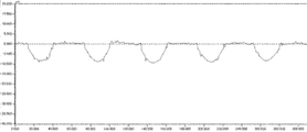
- FIG. 2 shows a cross-sectional curve when an opening having a diameter of 30 ⁇ m is filled with a conductive paste and sintered. The position of 0 ⁇ m on the vertical axis indicated by the broken line indicates the resist surface. From this figure, it became clear that the embedded conductive paste had a concave shape at the top. The center of the recess was dented to about 10 ⁇ m.
- About evaluation criteria A state in which the conductive paste is filled at a rate of 90 or more in 100 opening patterns. That is, the yield is 90% or more. :: A state in which the conductive paste is filled at a rate of 70 or more in 100 opening patterns. That is, the yield is 70% or more. ⁇ : A state in which 50 or more conductive pastes are filled in 100 opening patterns. That is, the yield is 50% or more. ⁇ : A state in which the conductive paste is filled in a proportion of less than 50 out of 100 opening patterns. That is, the yield is less than 50%.
- conductive pillars can be produced regardless of the type of protective agent and metal type.
- the same pillar can be formed not only in the diameter of the opening but also in a fine diameter of 20 ⁇ m.
- Example 4 Ethylene glycol, which was bubbled with nitrogen for 30 minutes, was added to the dry powder of the copper fine particle composite prepared by the method described in Example 1 in a glove bag purged with argon gas, and mixed in a mortar for 10 minutes to obtain a metal fine particle content of 90%. A conductive paste having a concentration of mass% was prepared.
- Example 5 To a dry copper fine particle composite powder produced by the method described in Example 1, ethylene glycol bubbled with nitrogen for 30 minutes was added in a glove bag purged with argon gas, and mixed in a mortar for 10 minutes to obtain a metal fine particle content of 70%. A conductive paste having a concentration of mass% was prepared.
- Example 6 Ethylene glycol, which was bubbled with nitrogen for 30 minutes, was added to the dry powder of the copper fine particle composite prepared by the method described in Example 1 in a glove bag purged with argon gas, and mixed in a mortar for 10 minutes to obtain a metal fine particle content of 40. A conductive paste having a concentration of mass% was prepared.
- Example 1 To a dry copper fine particle composite powder prepared by the method described in Example 1, ethylene glycol subjected to nitrogen bubbling for 30 minutes in a glove bag purged with argon gas was added, and mixed in a mortar for 10 minutes to obtain a metal fine particle content of 20%. A conductive paste having a concentration of mass% was prepared.
- Example 2 Ethylene glycol bubbled with nitrogen for 30 minutes was added to the dry powder of copper fine particles composite prepared by the method described in Example 1 in a glove bag purged with argon gas, and mixed in a mortar for 10 minutes to obtain a metal fine particle content of 95. A conductive paste having a concentration of mass% was prepared.
- Table 2 shows a list of evaluation results when the conductive pastes prepared by the methods described in Examples 4 to 6 and Comparative Examples 1 and 2 were embedded in a pattern having openings.
- the shape of the opening is cylindrical.
- the diameter is 100, 50, 40, 30, 20 ⁇ m, and the depth of the opening is 56 ⁇ m.
- the aspect ratios are 0.6, 1.1, 1.4, 1.9, and 2.8, respectively.
- embedding was performed using a rubber squeegee for screen printing. After filling the paste into the opening with a rubber squeegee, the paste was sintered at 250 ° C. for 10 minutes in an inert gas atmosphere. The surface state of the sintered film was observed and evaluated using an optical microscope and a laser microscope.
- About evaluation criteria A state in which the conductive paste is filled at a rate of 90 or more in 100 opening patterns. That is, the yield is 90% or more. :: A state in which the conductive paste is filled at a rate of 70 or more in 100 opening patterns. That is, the yield is 70% or more. ⁇ : A state in which 50 or more conductive pastes are filled in 100 opening patterns. That is, the yield is 50% or more. ⁇ : A state in which the conductive paste is filled in a proportion of less than 50 out of 100 opening patterns. That is, the yield is less than 50%.
Landscapes
- Chemical & Material Sciences (AREA)
- Dispersion Chemistry (AREA)
- Engineering & Computer Science (AREA)
- Nanotechnology (AREA)
- Physics & Mathematics (AREA)
- Spectroscopy & Molecular Physics (AREA)
- Chemical Kinetics & Catalysis (AREA)
- General Chemical & Material Sciences (AREA)
- Inorganic Chemistry (AREA)
- Conductive Materials (AREA)
- Non-Insulated Conductors (AREA)
Abstract
従来方法である電解メッキ法においてはアンダーカットの影響を受けずに微細なピラーを形成することが困難であるという問題があった。また、無電解メッキ法においてはボイドなく同一形状のピラーを形成することが困難であるという問題があった。そこで、本発明のピラー形成用導電ペーストを用いて、埋め込み法によりピラーを作製することにより、アンダーカットを防止できるとともに、再現性良く同一形状の金属ピラーを提供することを目的とする。 微細な金属微粒子であり、かつ、特定の微粒子の含有率を特徴とする導電ペーストがピラーの形成において、特段に効果があることを見出した。
Description
本発明は、半導体パッケージ内において、半導体チップとパッケージインターポーザの接続方式であるフリップチップ実装の端子である、金属ピラー(Pillar)あるいは金属ポスト(Post)用の金属微粒子を含有する導電ペーストに関する。
半導体装置においては、半導体チップ上に電子回路を形成し、半導体チップ上の電極と半導体パッケージ上の電極とを接続して形成される。従来、半導体チップ上の電極と半導体パッケージ上の電極との間は、金あるいは銅製のボンディングワイヤを用いて電気的に接続されていた。半導体チップと半導体パッケージの間の電気的な接続方法としてフリップチップ法が用いられている。フリップチップ法における代表的な接続方法として、金バンプやはんだバンプが用いられている。
しかしながら、近年のチップの高集積化に伴い、最近は銅ピラーを用いたフリップチップ技術が注目されている。銅ピラーは、半導体チップ上に形成し、銅ピラー先端を半導体パッケージの電極と接続する。銅ピラーとしては、ピラー直径70μm以下、ピラー高さが50~60μmのものが一般に用いられている。
銅ピラーは材質が低電気抵抗の銅であることから、はんだバンプに比べて大電流に対応できる。また、銅ピラーははんだバンプに比較してはんだ供給量を抑えることができるため、バンプピッチの微細化が可能である。さらに、金バンプは電極との接触面積が小さいのに対し、銅ピラーは半導体チップ上の電極から半導体パッケージ上の電極に至るまで同じ断面積を維持できることからも、大電流に対応可能であるという利点を有する。
上記理由により、銅ピラーの作製は半導体実装において重要であり、銅ピラーを簡便に作製する方法が望まれている。
しかしながら、近年のチップの高集積化に伴い、最近は銅ピラーを用いたフリップチップ技術が注目されている。銅ピラーは、半導体チップ上に形成し、銅ピラー先端を半導体パッケージの電極と接続する。銅ピラーとしては、ピラー直径70μm以下、ピラー高さが50~60μmのものが一般に用いられている。
銅ピラーは材質が低電気抵抗の銅であることから、はんだバンプに比べて大電流に対応できる。また、銅ピラーははんだバンプに比較してはんだ供給量を抑えることができるため、バンプピッチの微細化が可能である。さらに、金バンプは電極との接触面積が小さいのに対し、銅ピラーは半導体チップ上の電極から半導体パッケージ上の電極に至るまで同じ断面積を維持できることからも、大電流に対応可能であるという利点を有する。
上記理由により、銅ピラーの作製は半導体実装において重要であり、銅ピラーを簡便に作製する方法が望まれている。
基板上に銅ピラーを形成する方法として、メッキ技術を利用した方法が知られている。
シード層と呼ばれるメッキ層を電極パッド上に作製し、電解メッキにより銅ピラーを形成する方法である。しかしながら、メッキによりピラーを形成する場合、全面にシード層を設けるため、ピラー作製後にパターニングされたレジスト層及びシード層を除去する工程が必要となる。シード層をエッチングにより除去する工程において、アンダーカットによりメッキ法により微細なピラーを作製することは困難であるという課題が存在する 。
また、メッキ技術により銅ピラーを形成する方法として、無電解メッキを使用する方法もある。半導体チップ上にフォトレジスト層を形成し、銅ピラーを形成する部分のフォトレジスト層を開口し、開口部分に無電解で銅めっきを形成し、さらに銅めっきの頂部にはんだめっきを形成する方法である。しかしながら、当該方法において、銅ピラーの高さ/直径比(アスペクト比)が大きい細長い銅ピラーを形成するためには、直径が小さく深い穴にめっきを成長させる必要がある。この場合、開口部に十分な濃度のめっき液を送り続けることが難しく、めっきの成長が遅くなりスループットが悪化すること、銅ピラーの直径が目標より細くなるなど形状が不安定になること、析出する銅にボイドが生じること、などから品質及び再現性に問題が生じるという課題がある 。
シード層と呼ばれるメッキ層を電極パッド上に作製し、電解メッキにより銅ピラーを形成する方法である。しかしながら、メッキによりピラーを形成する場合、全面にシード層を設けるため、ピラー作製後にパターニングされたレジスト層及びシード層を除去する工程が必要となる。シード層をエッチングにより除去する工程において、アンダーカットによりメッキ法により微細なピラーを作製することは困難であるという課題が存在する 。
また、メッキ技術により銅ピラーを形成する方法として、無電解メッキを使用する方法もある。半導体チップ上にフォトレジスト層を形成し、銅ピラーを形成する部分のフォトレジスト層を開口し、開口部分に無電解で銅めっきを形成し、さらに銅めっきの頂部にはんだめっきを形成する方法である。しかしながら、当該方法において、銅ピラーの高さ/直径比(アスペクト比)が大きい細長い銅ピラーを形成するためには、直径が小さく深い穴にめっきを成長させる必要がある。この場合、開口部に十分な濃度のめっき液を送り続けることが難しく、めっきの成長が遅くなりスループットが悪化すること、銅ピラーの直径が目標より細くなるなど形状が不安定になること、析出する銅にボイドが生じること、などから品質及び再現性に問題が生じるという課題がある 。
また、メッキ法は大量の廃液を再生又は処分する必要があり、環境負荷が大きく設備維持にコストも要することから代替手段が望まれている。
したがって、従来方法である電解メッキ法においてはアンダーカットの影響を受けずに微細なピラーを形成することが困難であるという問題があった。また、無電解メッキ法においてはボイドなく同一形状のピラーを形成することが困難であるという問題があった。
本発明のピラー形成用導電ペーストを用いて、埋め込み法によりピラーを作製することにより、アンダーカットを防止できるとともに、再現性良く同一形状の金属ピラーを提供することを目的とする。
本発明者らは、前記諸問題を解決するために鋭意検討を重ねた結果、微細な金属微粒子であり、かつ、特定の金属微粒子の含有率を特徴とする導電ペーストがピラーの形成において、特段に効果があることを見出した。
すなわち本発明は、
(1)本発明は、金属微粒子と、保護剤と、を含むピラー形成用導電ペーストであって、前記金属微粒子の粒子径が1μm未満であり、かつ、前記導電ペースト中の金属微粒子含有率が40以上95質量%濃度未満であることを特徴とするピラー形成用導電ペーストである。
(1)本発明は、金属微粒子と、保護剤と、を含むピラー形成用導電ペーストであって、前記金属微粒子の粒子径が1μm未満であり、かつ、前記導電ペースト中の金属微粒子含有率が40以上95質量%濃度未満であることを特徴とするピラー形成用導電ペーストである。
(2)さらに沸点250℃以下の溶剤を含むことを特徴とする(1)記載のピラー形成用導電ペーストである。
(3)前記記載の保護剤として炭素数8~200のポリエチレンオキシド構造を含む有機化合物を含有することを特徴とする(1)又は(2)記載のピラー形成用導電ペーストである。
(4)前記記載の炭素数8~200のポリエチレンオキシド構造を含む有機化合物の含有率が全ペースト中15質量%濃度以下である、(1)~(3)いずれかに記載のピラー形成用導電ペースト。
(5)前記記載の金属微粒子の金属が、銀、銅又はこれらの複合体である、(1)から(4)いずれかに記載のピラー形成用導電ペースト。
(6)(1)から(5)いずれかに記載のピラー形成用導電ペーストを用いて作製されたピラー。
を提供するものである。
を提供するものである。
本発明は、充填法によりピラーを作製するための導電ペーストである。
本発明を用いることにより、従来技術であるメッキ技術を使用することなく、スキージ等であらかじめ導電ペーストをパターニングされたレジスト層の開口部分に充填させることでピラーを簡便に形成することができる。
導電ペーストを用いて電極基板上に直接ピラーを形成することにより、従来方法による課題であったエッチング時のアンダーカットを解決することができ、微細な銅ピラーの形成が可能となる。
導電ペーストによるピラー作製は、メッキ液の劣化や、イオンの拡散律速などの制限を受けないため、無電解メッキ法の品質や再現性の課題も解決できる可能性があると考えられる。
本発明を用いることにより、従来技術であるメッキ技術を使用することなく、スキージ等であらかじめ導電ペーストをパターニングされたレジスト層の開口部分に充填させることでピラーを簡便に形成することができる。
導電ペーストを用いて電極基板上に直接ピラーを形成することにより、従来方法による課題であったエッチング時のアンダーカットを解決することができ、微細な銅ピラーの形成が可能となる。
導電ペーストによるピラー作製は、メッキ液の劣化や、イオンの拡散律速などの制限を受けないため、無電解メッキ法の品質や再現性の課題も解決できる可能性があると考えられる。
以下、本発明を詳細に説明する。
<金属微粒子>
本発明の金属微粒子として用いることができる金属種は、当該金属種が後述する保護剤中の官能基と化学的に結合できるものであれば特に制限されない。例えば、金、銀、銅、ニッケル、亜鉛、アルミニウム、白金、パラジウム、スズ、クロム、鉛、タングステン等を用いることができる。また、金属種は一種類であっても、二種類以上の混合物、または合金であっても良い。
導電ペースト中の金属微粒子含有率は、40以上95質量%濃度未満の範囲で使用することができる。より好ましくは60~90質量%濃度の範囲で使用可能である。
本発明の金属微粒子として用いることができる金属種は、当該金属種が後述する保護剤中の官能基と化学的に結合できるものであれば特に制限されない。例えば、金、銀、銅、ニッケル、亜鉛、アルミニウム、白金、パラジウム、スズ、クロム、鉛、タングステン等を用いることができる。また、金属種は一種類であっても、二種類以上の混合物、または合金であっても良い。
導電ペースト中の金属微粒子含有率は、40以上95質量%濃度未満の範囲で使用することができる。より好ましくは60~90質量%濃度の範囲で使用可能である。
<保護剤>
本発明の保護剤は、金属微粒子や溶剤との親和性を有する官能基を有する化合物を任意に選択することができる。また、使用する保護剤は、分子量の大小にかかわらず使用することができる。使用する金属種や所望する物性に応じて保護剤を設計することで高導電性や分散安定性を金属微粒子に付与することが可能である。
本発明の保護剤は、金属微粒子や溶剤との親和性を有する官能基を有する化合物を任意に選択することができる。また、使用する保護剤は、分子量の大小にかかわらず使用することができる。使用する金属種や所望する物性に応じて保護剤を設計することで高導電性や分散安定性を金属微粒子に付与することが可能である。
具体的には、金属に対しやや強い吸着能を有するカルボキシ基、リン酸基、スルホン酸基、複素芳香族基(例えばイミダゾール基)等を有する保護剤を使用することにより、微粒子に高い分散安定性を付加することができる。
また、金属に対し中程度の相互作用を示し分散媒の液性によって吸着能が変化するアミノ基(例、ジメチルアミノエチル基、ジメチルアミノプロピル基)、ヒドロキシ基(ヒドロキシエチル基、ヒドロキシプロピル基)、芳香族基(たとえばベンジル基)等を有する保護剤を使用することにより、低温焼結においても低い体積抵抗率を発現する高導電性を付加することができる。
このように種々の目的に応じて金属微粒子用保護剤を選択することで金属微粒子の特性を自在に変更することができる。低分子量の保護剤を用いる場合は、二種以上の化合物を併用することで様々な特性を発現できる。高分子量の保護剤を用いる場合は、化合物中の官能基の数及び種類を変更することで様々な特性を発現できる。
また、金属に対し中程度の相互作用を示し分散媒の液性によって吸着能が変化するアミノ基(例、ジメチルアミノエチル基、ジメチルアミノプロピル基)、ヒドロキシ基(ヒドロキシエチル基、ヒドロキシプロピル基)、芳香族基(たとえばベンジル基)等を有する保護剤を使用することにより、低温焼結においても低い体積抵抗率を発現する高導電性を付加することができる。
このように種々の目的に応じて金属微粒子用保護剤を選択することで金属微粒子の特性を自在に変更することができる。低分子量の保護剤を用いる場合は、二種以上の化合物を併用することで様々な特性を発現できる。高分子量の保護剤を用いる場合は、化合物中の官能基の数及び種類を変更することで様々な特性を発現できる。
導電ペースト中の保護剤濃度は、全ペースト中15質量%濃度以下の範囲で使用することができる。より、好ましくは10質量%濃度以下の範囲である。保護剤濃度が高すぎる場合には、焼結時に金属粒子同士のネッキング現象が十分に生じず、高い導電性を発現させることが困難となる。
保護剤の具体例として以下の物質を例として列挙することができる、
例えば、カルボキシル基を有するカルボン酸としては、蟻酸、酢酸、プロピオン酸、酪酸、吉草酸、カプロン酸、エナント酸、カプリル酸、ペラルゴン酸、カプリン酸、ラウリン酸、ミリスチン酸、パルミチン酸、マルガリン酸、ステアリン酸、ベヘン酸、オレイン酸、パルミトオレイン酸、エイコセン酸、エルカ酸、ネルボン酸、リシノール酸、シュウ酸、マロン酸、コハク酸、グルタル酸、アジピン酸、ピメリン酸、スベリン酸、アゼライン酸、セバシン酸、ジグリコール酸、マレイン酸、イタコン酸、安息香酸、N-オレイルサルコシン、N-カルボベンゾキシ-4-アミノ酪酸、p-クマル酸、3-(4-ヒドロキシフェニル)プロピオン酸、3-ヒドロキシミリスチン酸、2-ヒドロキシパルミチン酸、2-ヒドロキシイコサン酸、2-ヒドロキシドコサン酸、2-ヒドロキシトリコサン酸、2-ヒドロキシテトラコサン酸、3-ヒドロキシカプロン酸、3-ヒドロキシオクタン酸、3-ヒドロキシノナン酸、3-ヒドロキシデカン酸、3-ヒドロキシウンデカン酸、3-ヒドロキシドデカン酸、3-ヒドロキシトリデカン酸、3-ヒドロキシテトラデカン酸、3-ヒドロキシヘキサデカン酸、3-ヒドロキシヘプタデカン酸、3-ヒドロキシオクタデカン酸、15-ヒドロキシペンタデカン酸、17-ヒドロキシヘプタデカン酸、15-ヒドロキシペンタデカン酸、17-ヒドロキシヘプタデカン酸、ラウロイルサルコシン、6-アミノヘキサン酸、2-ベンゾイル安息香酸、12-ヒドロキシステアリン酸、12-ヒドロキシペンタデカン酸、2-ヒドロキシパルミチン酸、3-ヒドロキシデカン酸、15-ヒドロキシペンタデカン酸、ラウロイルサルコシン、6-アミノヘキサン酸、N-(tert-ブトキシカルボニル)-6-アミノヘキサン酸、[2-(2-メトキシエトキシ)エトキシ]酢酸、N-カルボベンゾキシ-β-アラニン等を例示することができる。また、多量体を形成する化合物であれば、これらの二量体及び三量体から六量体までの多量体を用いても良い。また、1又は2以上のカルボン酸を任意の割合で組み合わせて用いることもできる。
例えば、カルボキシル基を有するカルボン酸としては、蟻酸、酢酸、プロピオン酸、酪酸、吉草酸、カプロン酸、エナント酸、カプリル酸、ペラルゴン酸、カプリン酸、ラウリン酸、ミリスチン酸、パルミチン酸、マルガリン酸、ステアリン酸、ベヘン酸、オレイン酸、パルミトオレイン酸、エイコセン酸、エルカ酸、ネルボン酸、リシノール酸、シュウ酸、マロン酸、コハク酸、グルタル酸、アジピン酸、ピメリン酸、スベリン酸、アゼライン酸、セバシン酸、ジグリコール酸、マレイン酸、イタコン酸、安息香酸、N-オレイルサルコシン、N-カルボベンゾキシ-4-アミノ酪酸、p-クマル酸、3-(4-ヒドロキシフェニル)プロピオン酸、3-ヒドロキシミリスチン酸、2-ヒドロキシパルミチン酸、2-ヒドロキシイコサン酸、2-ヒドロキシドコサン酸、2-ヒドロキシトリコサン酸、2-ヒドロキシテトラコサン酸、3-ヒドロキシカプロン酸、3-ヒドロキシオクタン酸、3-ヒドロキシノナン酸、3-ヒドロキシデカン酸、3-ヒドロキシウンデカン酸、3-ヒドロキシドデカン酸、3-ヒドロキシトリデカン酸、3-ヒドロキシテトラデカン酸、3-ヒドロキシヘキサデカン酸、3-ヒドロキシヘプタデカン酸、3-ヒドロキシオクタデカン酸、15-ヒドロキシペンタデカン酸、17-ヒドロキシヘプタデカン酸、15-ヒドロキシペンタデカン酸、17-ヒドロキシヘプタデカン酸、ラウロイルサルコシン、6-アミノヘキサン酸、2-ベンゾイル安息香酸、12-ヒドロキシステアリン酸、12-ヒドロキシペンタデカン酸、2-ヒドロキシパルミチン酸、3-ヒドロキシデカン酸、15-ヒドロキシペンタデカン酸、ラウロイルサルコシン、6-アミノヘキサン酸、N-(tert-ブトキシカルボニル)-6-アミノヘキサン酸、[2-(2-メトキシエトキシ)エトキシ]酢酸、N-カルボベンゾキシ-β-アラニン等を例示することができる。また、多量体を形成する化合物であれば、これらの二量体及び三量体から六量体までの多量体を用いても良い。また、1又は2以上のカルボン酸を任意の割合で組み合わせて用いることもできる。
例えば、アミノ基を有するアミンとしては、2-メトキシエチルアミン、2-エトキシエチルアミン、2-イソプロポキシエチルアミン、3-メトキシプロピルアミン、3-エトキシプロピルアミン、3-イソプロポキシプロピルアミン、3-(2-エチルヘキシルオキシ)プロピルアミン、N-メチルエチレンジアミン、N-エチルエチレンジアミン、N-イソプロピルエチレンジアミン、N-メチル-1,3-プロパンジアミン、3-イソプロピルアミノプロピルアミン、N,N-ジメチルエチレンジアミン、N,N-ジエチルエチレンジアミン、N,N-ジメチル-1,3-プロパンジアミン、N,N-ジエチル-1,3-プロパンジアミン、N-(3-アミノプロピル)モルホリン、N-(tert-ブトキシカルボニル)-1,4-ジアミノブタン、N-(tert-ブトキシカルボニル)-1,5-ジアミノペンタン、N-(tert-ブトキシカルボニル)-1,6-ジアミノヘキサン、2-(アミノエチルアミノ)エタノール、2-(アミノエトキシ)エタノール、3-(2-ヒドロキシエチルアミノ)プロピルアミン、N-(2-ヒドロキシプロピル)エチレンジアミン、N-(3-アミノプロピル)ジエタノールアミン等を例示することができる。この他に、アミン類として第二級アミン化合物、又は、第三級アミン化合物も併用することができる。
本発明で用いる保護剤の一例として、炭素数8~200のポリエチレンオキシド構造を含む有機化合物を用いることができる。当該保護剤のポリエチレンオキシド部位は、沸点が250℃以下のアルコール系溶媒など本発明で用いる特定の溶媒との親和性に優れることから、金属微粒子の凝集を強く抑制でき、金属微粒子の高分散を可能とする。これは即ち、金属微粒子が高密度に充填されている状態であるため、加熱処理による保護剤及び溶媒の分解除去に伴うボイド発生を起こさず、高密度充填を可能とする。
また、本発明の保護剤を用いて合成した金属微粒子は、保護剤存在量が2~10質量%濃度程度と少なく、焼成時の金属粒子同士のネッキング現象を妨げない。
また、本発明の保護剤を用いて合成した金属微粒子は、保護剤存在量が2~10質量%濃度程度と少なく、焼成時の金属粒子同士のネッキング現象を妨げない。
本発明で用いられる炭素数8~200のポリエチレンオキシド構造を含む有機化合物を含有する金属微粒子(有機化合物と金属微粒子の複合体)の例として、特許第4784847号公報、特開2013-60637号公報又は特許第5077728号公報が挙げられ、ここに記載の方法で合成することができる。これらは、チオエーテル型(R-S-R’)化合物が金属粒子表面に対して適切な親和吸着効果と、加熱による迅速な脱離性を有することが特徴となっており、低温融着特性を示す金属微粒子として開発されている。
また、他の例として、特開2010-209421号公報に記載のチオエーテル基を有する高分子化合物のうち、炭素数8~200のポリエチレンオキシド部位を有する高分子化合物が複合した金属微粒子、さらには、特許第4697356号公報に記載のチオエーテル基を有しリン酸エステル基を有する高分子化合物のうち、炭素数8~200のポリエチレンオキシド部位を有する高分子化合物が複合した金属微粒子などが挙げられる。これらのポリエチレンオキシド構造を含む高分子化合物の製造は、これら公報に記載の方法に従い行うことができる。
また、本発明においてこれらのポリエチレンオキシド構造を含むリン酸エステル型有機化合物は、チオエーテル基を有しリン酸エステル基をも有しており、これらの基を有することにより、金属微粒子表面に対して適切な親和吸着効果と、加熱による迅速な脱離性を付加することができる。
また、本発明においてこれらのポリエチレンオキシド構造を含むリン酸エステル型有機化合物は、チオエーテル基を有しリン酸エステル基をも有しており、これらの基を有することにより、金属微粒子表面に対して適切な親和吸着効果と、加熱による迅速な脱離性を付加することができる。
エチレンオキシド構造を繰り返し単位として有する鎖状の官能基は、溶媒親和部として機能する。このポリエチレンオキシド構造の炭素数は、8~200のものを用いることが好適であり、炭素数8~100のものを用いることがより好適である。
<溶媒>
本発明で用いることができる溶媒としては、沸点が250℃以下の化合物であれば分子量の大小にかかわらず、特に制限されることはない。水又は/及び有機溶剤を溶媒として用いることが可能である。前記溶媒は、金属微粒子を凝集させない良溶媒を用いることが、均一な粒子系を有する導電ペーストを製造する上では好ましい。
本発明で用いることができる溶媒としては、沸点が250℃以下の化合物であれば分子量の大小にかかわらず、特に制限されることはない。水又は/及び有機溶剤を溶媒として用いることが可能である。前記溶媒は、金属微粒子を凝集させない良溶媒を用いることが、均一な粒子系を有する導電ペーストを製造する上では好ましい。
溶媒は、導電ペースト焼結時に揮発することが望ましい。しかし、高い焼結温度はレジスト膜を変質させ、ダメージを与えてしまう。したがって、レジスト膜へのダメージが生じない温度範囲に沸点を有する有機溶剤を溶媒として使用することがより望ましい。
以下に、特に好適に用いることができる有機溶剤について例示列挙するが、本発明はこれら化合物に限定されるものではない。
例えば、水酸基を含む有機溶剤としてメタノール、エタノール、1-プロパノール、イソプロパノール、1-ブタノール、イソブタノール、sec-ブタノール、tert-ブタノール、アミルアルコール、tert-アミルアルコール、1-ヘキサノール、シクロヘキサノール、ベンジルアルコール、2-エチル-1-ブタノール、1-ヘプタノール、1-オクタノール、4-メチル-2-ペンタノール、ネオペンチルグリコール、プロピオニトリル、エチレングリコール、プロピレングリコール、1,3-ブタンジオール、1,4-ブタンジオール、2,3-ブタンジオール、イソブチレングリコール、2,2-ジメチル-1,3-ブタンジオール、2-メチル-1,3-ペンタンジオール、2-メチル-2,4-ペンタンジオール、ジエチレングリコール、トリエチレングリコール、テトラエチレングリコール、1,5-ペンタンジオール、2,4-ペンタンジオール、ジプロピレングリコール、2,5-ヘキサンジオール、グリセリン、ジエチレングリコールモノブチルエーテル、エチレングリコールモノベンジルエーテル、エチレングリコールモノエチルエーテル、エチレングリコールモノメチルエーテル、エチレングリコールモノフェニルエーテル、プロピレングリコールジメチルエーテル、ポリエチレングリコール、ポリプロピレングリコールなどを例示することができる。
その他、水酸基を含まない有機溶剤として、アセトン、シクロペンタノン、シクロヘキサノン、アセトフェノン、アクリロニトリル、プロピオニトリル、n-ブチロニトリル、イソブチロニトリル、γ-ブチロラクトン、ε-カプロラクト、プロピオラクトン、炭酸-2,3-ブチレン、炭酸エチレン、炭酸1,2-エチレン、炭酸ジメチル、炭酸エチレン、マロン酸ジメチル、乳酸エチル、安息香酸メチル、サリチル酸メチル、二酢酸エチレングリコール、ε-カプロラクタム、ジメチルスルホキシド、N,N-ジメチルホルムアミド、N,N-ジメチルアセトアミド、N-メチルホルムアミド、N-メチルアセトアミド、N-エチルアセトアミド、N,N-ジエチルホルムアミド、ホルムアミド、ピロリジン、1-メチル-2-ピロリジノン、ヘキサメチルリン酸トリアミド、ナフタレンも例示することができる。
その他、水酸基を含まない有機溶剤として、アセトン、シクロペンタノン、シクロヘキサノン、アセトフェノン、アクリロニトリル、プロピオニトリル、n-ブチロニトリル、イソブチロニトリル、γ-ブチロラクトン、ε-カプロラクト、プロピオラクトン、炭酸-2,3-ブチレン、炭酸エチレン、炭酸1,2-エチレン、炭酸ジメチル、炭酸エチレン、マロン酸ジメチル、乳酸エチル、安息香酸メチル、サリチル酸メチル、二酢酸エチレングリコール、ε-カプロラクタム、ジメチルスルホキシド、N,N-ジメチルホルムアミド、N,N-ジメチルアセトアミド、N-メチルホルムアミド、N-メチルアセトアミド、N-エチルアセトアミド、N,N-ジエチルホルムアミド、ホルムアミド、ピロリジン、1-メチル-2-ピロリジノン、ヘキサメチルリン酸トリアミド、ナフタレンも例示することができる。
導電ペースト中の溶媒濃度は、60質量%濃度以下の範囲で使用することができる。より、好ましくは30質量%濃度以下の範囲である。
(混合物の沸点測定方法)
複数の溶媒を組み合わせた混合溶媒を用いる場合、前期混合溶媒(溶液)の沸点は、JIS K2233-1989「自動車用非鉱油系ブレーキ液」7.1に規定する「平衡還流沸点試験方法」に準じて測定することができる。
具体例をあげると、
(1)100mL三つ口フラスコに、2種の溶媒を混合した混合溶液60mLと撹拌子を入れる。
(2)オイルバスの液面とフラスコ内の液面をあわせ、オイルバスを用いて加熱する。
(3)内溶液に気泡が発生した時点の内温を読み取り、混合溶液の沸点とする。
上記具体例に沿って見積もられた沸点を溶媒の沸点として採用することができる。二種以上の溶媒を組み合わせた混合溶媒を本発明に使用する場合には、混合溶媒の沸点が250℃以下であれば特に制限されることはない。
複数の溶媒を組み合わせた混合溶媒を用いる場合、前期混合溶媒(溶液)の沸点は、JIS K2233-1989「自動車用非鉱油系ブレーキ液」7.1に規定する「平衡還流沸点試験方法」に準じて測定することができる。
具体例をあげると、
(1)100mL三つ口フラスコに、2種の溶媒を混合した混合溶液60mLと撹拌子を入れる。
(2)オイルバスの液面とフラスコ内の液面をあわせ、オイルバスを用いて加熱する。
(3)内溶液に気泡が発生した時点の内温を読み取り、混合溶液の沸点とする。
上記具体例に沿って見積もられた沸点を溶媒の沸点として採用することができる。二種以上の溶媒を組み合わせた混合溶媒を本発明に使用する場合には、混合溶媒の沸点が250℃以下であれば特に制限されることはない。
<金属微粒子の合成>
本発明の金属微粒子の合成方法としては、化学還元方法を採用したが、金属微粒子表面を保護剤より保護することができ、かつ、粒子径が1μm以下であれば、任意の方法を採用することができる。例えば、湿式法として化学還元法のほかに熱分解法、電気化学法を採用することもできる。乾式法としてガス中蒸発法、スパッタ法を採用することもできる。
本発明の金属微粒子の合成方法としては、化学還元方法を採用したが、金属微粒子表面を保護剤より保護することができ、かつ、粒子径が1μm以下であれば、任意の方法を採用することができる。例えば、湿式法として化学還元法のほかに熱分解法、電気化学法を採用することもできる。乾式法としてガス中蒸発法、スパッタ法を採用することもできる。
本発明の効果を説明する一例として、以下に本発明で使用する保護剤として炭素数8~200のポリエチレンオキシド構造を含む有機化合物を使用した際の金属微粒子の製造方法について説明する。
前記製造方法の具体例を示すにあたり、金属種を銅又は銀とした場合について記述するが、本発明の導電ペーストの金属種を銅又は銀に限定するわけではない。
炭素数8~200のポリエチレンオキシド構造を含む有機化合物が複合した金属微粒子は、チオエーテル型有機化合物の存在下で、2価の銅イオン化合物又は1価の銀イオン化合物を溶媒と混合する工程と、銅イオン又は銀イオンを還元する工程と組み合わせることで容易に作製することが可能である。
前記製造方法の具体例を示すにあたり、金属種を銅又は銀とした場合について記述するが、本発明の導電ペーストの金属種を銅又は銀に限定するわけではない。
炭素数8~200のポリエチレンオキシド構造を含む有機化合物が複合した金属微粒子は、チオエーテル型有機化合物の存在下で、2価の銅イオン化合物又は1価の銀イオン化合物を溶媒と混合する工程と、銅イオン又は銀イオンを還元する工程と組み合わせることで容易に作製することが可能である。
2価の銅イオン化合物としては、一般的に入手可能な銅化合物が利用可能であり、硫酸塩、硝酸塩、カルボン酸塩、炭酸塩、塩化物、アセチルアセトナート錯体等が利用できる。0価の銅微粒子との複合体を得る場合には2価の化合物から出発しても1価の化合物から製造してもよく、水分や結晶水を有していても差し支えない。具体的には、結晶水を除いて表現すれば、CuSO4、Cu(NO3)2、Cu(OAc)2、Cu(CH3CH2COO)2、Cu(HCOO)2、CuCO3、CuCl2、Cu2O、C5H7CuO2などが挙げられる。さらに、上記塩類を加熱したり、塩基性雰囲気に曝したりすることにより得られる塩基性塩、たとえばCu(OAc)2・CuO、Cu(OAc)2・2CuO、Cu2Cl(OH)3等は最も好適に用いることができる。これら塩基性塩は、反応系内で調製してもよいし、反応系外で別途調製したものを使用してもよい。また、アンモニアやアミン化合物を加えて錯体形成し、溶解度を確保してから還元に用いる一般的な方法も適用可能である。
1価の銀イオン化合物としては、一般的に入手可能な銀化合物が利用可能であり、硝酸銀、酸化銀、酢酸銀、フッ化銀、銀アセチルアセトナート、安息香酸銀、炭酸銀、クエン酸銀、銀ヘキサフルオロフォスフェート、乳酸銀、亜硝酸銀、ペンタフルオロプロピオン酸銀等が挙げられ、取り扱い容易性、工業的入手容易性の観点から、硝酸銀または酸化銀を用いることが好ましい。
これらの銅又は銀イオン化合物を、予めチオエーテル型有機化合物を溶解又は分散した媒体に溶解、または混合する。このとき用いることができる媒体としては、使用する有機化合物の構造にもよるが、水、エタノール、アセトン、エチレングリコール、ジエチレングリコール、グリセリンおよびそれらの混合物が好適に用いられ、水-エチレングリコール混合物は特に好ましい。
チオエーテル型有機化合物の、各種媒体中における濃度としては、引き続き行なう還元反応の制御が容易になる点から、0.3~10質量%濃度の範囲に調整することが好ましい。
上記で調整した媒体中に、前記銅又は銀イオン化合物を、一括又は分割して添加し、混合する。溶解しにくい媒体を使用する場合には、予め少量の良溶媒に溶解させておいてから、媒体中に添加する方法であっても良い。
混合するチオエーテル型有機化合物と銅又は銀イオン化合物との使用割合としては、反応媒体中でのチオエーテル型有機化合物の保護能力に応じて適宜選択することが好ましいが、通常、銅又は銀イオン化合物1molあたりに、チオエーテル型有機化合物として1mmol~30mmol(分子量2000のポリマーを用いる場合、2~60g程度)の範囲で調製し、特に15~30mmolの範囲で用いることが好ましい。ここで、ポリエチレンオキシド構造を含むリン酸エステル型有機化合物を用いても同様に行うことができ、銅又は銀イオン化合物1molあたりの有機化合物の使用量も前期と同様である。
引き続き、銅又は銀イオンの還元を、各種還元剤を用いて行なう。還元剤としては、ヒドラジン化合物、ヒドロキシルアミンおよびその誘導体、金属水素化物、ホスフィン酸塩類、アルデヒド類、エンジオール類、ヒドロキシケトン類など、氷冷温から80℃以下の温度で銅又は銀の還元反応を進行させることができる化合物であることが、沈殿物形成の少ない複合体を与えるため、好適である。
銅イオンの還元において、具体的にはヒドラジン水和物、非対称ジメチルヒドラジン、ヒドロキシルアミン水溶液、水素化ホウ素ナトリウムなどの強力な還元剤が好適である。これらは、銅化合物を0価まで還元する能力を有するので、2価および1価の銅化合物を還元銅とし、有機化合物とナノ銅粒子との複合体を製造する場合に適している。
還元反応に適する条件は、原料として用いる銅化合物、還元剤の種類、錯化の有無、媒体、チオエーテル型有機化合物の種類によって様々である。例えば、水系で酢酸銅(II)を水素化ホウ素ナトリウムで還元する場合には、氷冷程度の温度でも0価のナノ銅粒子が調製できる。一方、ヒドラジンを用いる場合には、室温では反応は遅く、60℃程度に加熱してはじめて円滑な還元反応が起こり、エチレングリコール/水系で酢酸銅を還元する場合には、60℃で2時間程度の反応時間を要する。このようにして還元反応が終了すると、有機化合物と銅系微粒子との複合体を含む反応混合物が得られる。
このように調製した銅微粒子は保護剤の効果により、水分を完全に除去して乾燥体粉末とした後に、再び溶媒を添加しても乾燥前の状態と同じように高分散させることが可能である。
また、チオエーテル型有機化合物と前記媒体、および銅イオン化合物の混合液中にナノ銀を添加した混合液をあらかじめ調整し、次いで還元剤を添加して銅イオンを前記方法で還元させると、ナノ銀表面を銅が被覆した、銀コア銅シェル微粒子を得ることができる。
また、逆にチオエーテル型有機化合物と前記媒体、および銀イオン化合物の混合液中にナノ銅を添加した混合液をあらかじめ調整し、次いで還元剤を添加して銀イオンを前記方法で還元させると、ナノ銅表面を銀が被覆した、銅コア銀シェル微粒子を得ることができる。
還元反応後は、必要に応じて金属化合物残渣、還元試薬残渣、余剰のポリエチレンオキシド構造を含む有機化合物等を除く工程が設けられる。複合体の精製には、再沈殿、遠心沈降または限外濾過が適用可能であり、得られた複合体を含む反応混合物を洗浄溶媒、例えば水、エタノール、アセトンおよびこれらの混合物によって洗浄することで、前述の不純物を洗い流すことができる。
<ピラー形成用導電ペーストの作製>
本発明のピラー形成用導電ペーストは、作製した金属微粒子に充填用のペーストとして使い易い溶媒を加え、あるいは、媒体交換することにより、本発明の導電ペーストとしての適性を付与することができる。
本発明のピラー形成用導電ペーストは、作製した金属微粒子に充填用のペーストとして使い易い溶媒を加え、あるいは、媒体交換することにより、本発明の導電ペーストとしての適性を付与することができる。
本発明のピラー形成用導電ペーストには、本発明の効果を損なわせない範囲において、必要に応じて、樹脂等のバインダー成分、乾燥防止剤、消泡剤、基材への密着付与剤、酸化防止剤、皮膜形成促進のための各種触媒、シリコーン系界面活性剤、フッ素系界面活性剤の様な各種界面活性剤、レベリング剤、離型促進剤等を助剤として添加できる。
本発明の導電ペーストは、本発明の効果を損なわない範囲内でフラックス成分を加えることができる。フラックス成分を加えることにより、一層の還元力を持たせて使用することもできる。フラックスとしては、通常用いられる一般的なフラックスを用いることが可能であり、特に制限するものではない。このフラックス中には、通常用いられるロジン、活性剤、チキソ剤等が含まれていても構わない。
<金属微粒子含有率の計算>
本発明における導電ペースト中の金属微粒子を含有率は、熱重量分析(TG/DTA)により算出することができる。導電ペーストを熱重量分析用アルミパンに精密にはかり、示差熱重量分析装置に載せ、不活性ガス雰囲気下において、室温~600℃まで毎分10℃の割合で昇温して、重量減少率に基づいて金属微粒子含有率を計算した。
本発明における導電ペースト中の金属微粒子を含有率は、熱重量分析(TG/DTA)により算出することができる。導電ペーストを熱重量分析用アルミパンに精密にはかり、示差熱重量分析装置に載せ、不活性ガス雰囲気下において、室温~600℃まで毎分10℃の割合で昇温して、重量減少率に基づいて金属微粒子含有率を計算した。
<ピラーの形成方法>
本発明におけるピラーの形成方法については、特に制限されるものではない。例えば、簡便にピラーを形成する方法として、開口部を複数有する基板の開口部分に導電ペーストを充填し、焼結することで作製することもできる。
基板として用いる材料に特に制限は無いが、金属、シリコン、セラミック、樹脂、及びこれらの複合材料等を用いることができる。前記基板上にレジスト膜を作製し、開口部をパターニングすることによって開口部を複数有する基板を作製することができる。レジスト膜は、ピラー形成後に除去しても良いが、永久膜として残存させておくこともできる。
導電ペーストの充填方法としては、特に制限されるものではなく、ゴムスキージ、ドクターブレード、ディスペンサ、インクジェット、プレス注入等を採用することができる。
本発明におけるピラーの形成方法については、特に制限されるものではない。例えば、簡便にピラーを形成する方法として、開口部を複数有する基板の開口部分に導電ペーストを充填し、焼結することで作製することもできる。
基板として用いる材料に特に制限は無いが、金属、シリコン、セラミック、樹脂、及びこれらの複合材料等を用いることができる。前記基板上にレジスト膜を作製し、開口部をパターニングすることによって開口部を複数有する基板を作製することができる。レジスト膜は、ピラー形成後に除去しても良いが、永久膜として残存させておくこともできる。
導電ペーストの充填方法としては、特に制限されるものではなく、ゴムスキージ、ドクターブレード、ディスペンサ、インクジェット、プレス注入等を採用することができる。
本発明の導電ペーストを、基板の開口部分充填し、金属微粒子が融着する温度まで加熱し、ピラーを作製することができる。このとき、酸化しやすい金属を材料として用いる場合には、水素を含むフォーミングガス下、窒素雰囲気下又はギ酸を通過させて含ませたギ酸を含む窒素の雰囲気下のいずれでも行うことができる。
本発明のピラー形成用導電ペーストは、加熱焼結時に加圧を必要とせず、開口部に充填し焼結するだけで、十分な性能を発揮できる。
本発明のピラー形成用導電ペーストは、加熱焼結時に加圧を必要とせず、開口部に充填し焼結するだけで、十分な性能を発揮できる。
また、塗布を0.9~0.01気圧(900hPa~1hPa)の減圧雰囲気下で行い、その後常圧に戻すことで、開口部に導電ペーストを押し込むこともできる。
焼成温度は150~350℃の範囲であれば融着可能であり、焼成時間は1~60分間の範囲あれば十分な性能を発揮するが、作業を短時間にする点、及び、その後のレジスト膜の除去を考えると250℃以下で5~15分間の焼成が好ましい。本発明の導電ペーストを使用すれば、短時間焼成においても十分な性能を発揮することができる。
また、必要に応じて、低温で溶媒を揮発させる仮焼成を行ってから、150~350℃の範囲で本焼成を行う等の、温度プロファイルを用いて焼成を行うこともできる。
また、必要に応じて、低温で溶媒を揮発させる仮焼成を行ってから、150~350℃の範囲で本焼成を行う等の、温度プロファイルを用いて焼成を行うこともできる。
ここで、導電ペースト中の金属微粒子含有率が40質量%濃度未満の場合、開口部に充填し、焼結させた場合に、金属成分が少なすぎるために金属微粒子同士の融着が進まない。したがって、レジスト剥離後にピラーが自立できないばかりではなく、導電性も十分に発揮されない、という問題が生じる。
以上より、金属微粒子を含む率は少なくとも40質量%濃度有することが好ましい。
以上より、金属微粒子を含む率は少なくとも40質量%濃度有することが好ましい。
導電ペースト中の金属微粒子含有率が95質量%濃度を超える場合、高い粘度及びチキソトロピー性により、高アスペクト比の開口部へ均一かつ空隙無く充填することは難しい。また、本発明の特徴であるピラー上部の形状を凹型にすることは難しい。
以上より、金属微粒子を含む率は95質量%濃度以下とすることが好ましい。
以上より、金属微粒子を含む率は95質量%濃度以下とすることが好ましい。
以下、実施例をもって本発明を具体的に説明する。ここで「%」は、特に指定がない限り「質量%」である。
〔熱重量分析による重量減少率の測定〕
導電ペースト2~25mgを熱重量分析用アルミパンに精密にはかり、EXSTAR TG/DTA6300型示差熱重量分析装置(エスアイアイ・ナノテクノロジー株式会社製)に載せ、不活性ガス雰囲気下において、室温~600℃まで毎分10℃の割合で昇温して、100℃~600℃の重量減少率を測定した。前記重量減少率より金属微粒子含有率及び保護剤の含有率を計算した。
導電ペースト2~25mgを熱重量分析用アルミパンに精密にはかり、EXSTAR TG/DTA6300型示差熱重量分析装置(エスアイアイ・ナノテクノロジー株式会社製)に載せ、不活性ガス雰囲気下において、室温~600℃まで毎分10℃の割合で昇温して、100℃~600℃の重量減少率を測定した。前記重量減少率より金属微粒子含有率及び保護剤の含有率を計算した。
(実施例1)
酢酸銅(II)一水和物(3.00g、15.0mmol)(東京化成工業社製)、エチル3-(3-(メトキシ(ポリエトキシ)エトキシ)-2-ヒドロキシプロピルスルファニル)プロピオナート〔ポリエチレングリコールメチルグリシジルエーテル(ポリエチレングリコール鎖の分子量2000(炭素数91))への3-メルカプトプロピオン酸エチルの付加化合物〕(0.451g)(DIC社製)、およびエチレングリコール(10mL)(関東化学社製)からなる混合物に、窒素を50mL/分の流量で吹き込みながら加熱し、125℃で2時間通気攪拌して脱気した。この混合物を室温に戻し、ヒドラジン水和物(1.50g、30.0mmol)(東京化成工業社製)を水7mLで希釈した溶液を、シリンジポンプを用いてゆっくり滴下した。約1/4量を2時間かけてゆっくり滴下し、ここで一旦滴下を停止し、2時間攪拌して発泡が沈静化するのを確認した後、残量を更に1時間かけて滴下した。得られた褐色の溶液を60℃に昇温して、さらに2時間攪拌し、還元反応を終結させた。
<水分散液の調製>
つづいて、この反応混合物をダイセン・メンブレン・システムズ社製の中空糸型限外濾過膜モジュール(HIT-1-FUS1582、145cm2、分画分子量15万)中に循環させ、滲出する濾液と同量の0.1%ヒドラジン水和物水溶液を加えながら、限外濾過モジュールからの濾液が約500mLとなるまで循環させて精製した。0.1%ヒドラジン水和物水溶液の供給を止め、そのまま限外濾過法により濃縮すると、2.85gのチオエーテルを含む有機化合物と銅微粒子との複合体の水分散液が得られた。
得られた銅微粒子を透過型電子顕微鏡(TEM)により観察すると、得られた銅微粒子の一次粒子径は20nmであった。水分散液中の不揮発物含量は16質量%濃度であった。TG-DTA測定による重量減少より、得られた銅微粒子には3%のポリエチレンオキシド構造を含む有機物が存在していた。
<導電ペーストの調製>
上記の水分散液5mLをそれぞれ50mL三口フラスコに封入し、ウォーターバスを用いて40℃に加温を行いながら、減圧下、窒素を5ml/minの流速で流すことで、水を完全に除去し、銅微粒子複合体乾燥粉末1.0gを得た。次に得られた乾燥粉末にアルゴンガス置換したグローブバッグ内で、30分間窒素バブリングしたエチレングリコールを添加し、乳鉢で10分間混合することで金属微粒子含有率80質量%濃度の導電ペーストを作製した。また、表面張力を調整するためにフッ素系レベリング剤MEGAFACE(DIC社製)を添加した。
酢酸銅(II)一水和物(3.00g、15.0mmol)(東京化成工業社製)、エチル3-(3-(メトキシ(ポリエトキシ)エトキシ)-2-ヒドロキシプロピルスルファニル)プロピオナート〔ポリエチレングリコールメチルグリシジルエーテル(ポリエチレングリコール鎖の分子量2000(炭素数91))への3-メルカプトプロピオン酸エチルの付加化合物〕(0.451g)(DIC社製)、およびエチレングリコール(10mL)(関東化学社製)からなる混合物に、窒素を50mL/分の流量で吹き込みながら加熱し、125℃で2時間通気攪拌して脱気した。この混合物を室温に戻し、ヒドラジン水和物(1.50g、30.0mmol)(東京化成工業社製)を水7mLで希釈した溶液を、シリンジポンプを用いてゆっくり滴下した。約1/4量を2時間かけてゆっくり滴下し、ここで一旦滴下を停止し、2時間攪拌して発泡が沈静化するのを確認した後、残量を更に1時間かけて滴下した。得られた褐色の溶液を60℃に昇温して、さらに2時間攪拌し、還元反応を終結させた。
<水分散液の調製>
つづいて、この反応混合物をダイセン・メンブレン・システムズ社製の中空糸型限外濾過膜モジュール(HIT-1-FUS1582、145cm2、分画分子量15万)中に循環させ、滲出する濾液と同量の0.1%ヒドラジン水和物水溶液を加えながら、限外濾過モジュールからの濾液が約500mLとなるまで循環させて精製した。0.1%ヒドラジン水和物水溶液の供給を止め、そのまま限外濾過法により濃縮すると、2.85gのチオエーテルを含む有機化合物と銅微粒子との複合体の水分散液が得られた。
得られた銅微粒子を透過型電子顕微鏡(TEM)により観察すると、得られた銅微粒子の一次粒子径は20nmであった。水分散液中の不揮発物含量は16質量%濃度であった。TG-DTA測定による重量減少より、得られた銅微粒子には3%のポリエチレンオキシド構造を含む有機物が存在していた。
<導電ペーストの調製>
上記の水分散液5mLをそれぞれ50mL三口フラスコに封入し、ウォーターバスを用いて40℃に加温を行いながら、減圧下、窒素を5ml/minの流速で流すことで、水を完全に除去し、銅微粒子複合体乾燥粉末1.0gを得た。次に得られた乾燥粉末にアルゴンガス置換したグローブバッグ内で、30分間窒素バブリングしたエチレングリコールを添加し、乳鉢で10分間混合することで金属微粒子含有率80質量%濃度の導電ペーストを作製した。また、表面張力を調整するためにフッ素系レベリング剤MEGAFACE(DIC社製)を添加した。
(実施例2)
硝酸銅(東京化成工業社製)5.6g、保護剤としてオクチルアミン(東京化成工業社製)9.2g、リノール酸(東京化成工業社製)2.1gをトリメチルペンタン(東京化成工業社製)1リットルに加え、攪拌混合し溶解した。この混合溶液に、0.01モル/リットルの水素化ホウ素ナトリウム(東京化成工業社製)を含むプロパノール(東京化成工業社製)溶液1リットルを1時間かけて滴下し銅を還元した。さらに、3時間攪拌して黒色の液体を得た。得られた黒色の液体をエバポレーターによって濃縮した後、これにメタノール2リットルを加えて褐色の沈殿物を生成させた後、吸引ろ過により沈殿物を回収した。生成した沈殿物をトリメチルペンタンに再分散させ、ろ過した後、乾燥させて、銅微粒子を黒色の固体として得た。得られた銅微粒子を透過型電子顕微鏡(TEM)により観察すると、得られた銅微粒子の一次粒子径は6nmであった。次に、TG-DTA測定による重量減少より、得られた銅微粒子には15%の有機物が存在していることを確認した。
硝酸銅(東京化成工業社製)5.6g、保護剤としてオクチルアミン(東京化成工業社製)9.2g、リノール酸(東京化成工業社製)2.1gをトリメチルペンタン(東京化成工業社製)1リットルに加え、攪拌混合し溶解した。この混合溶液に、0.01モル/リットルの水素化ホウ素ナトリウム(東京化成工業社製)を含むプロパノール(東京化成工業社製)溶液1リットルを1時間かけて滴下し銅を還元した。さらに、3時間攪拌して黒色の液体を得た。得られた黒色の液体をエバポレーターによって濃縮した後、これにメタノール2リットルを加えて褐色の沈殿物を生成させた後、吸引ろ過により沈殿物を回収した。生成した沈殿物をトリメチルペンタンに再分散させ、ろ過した後、乾燥させて、銅微粒子を黒色の固体として得た。得られた銅微粒子を透過型電子顕微鏡(TEM)により観察すると、得られた銅微粒子の一次粒子径は6nmであった。次に、TG-DTA測定による重量減少より、得られた銅微粒子には15%の有機物が存在していることを確認した。
次に、得られた銅微粒子乾燥粉末1.0gにアルゴンガス置換したグローブバッグ内で、30分間窒素バブリングしたテルピネオール(和光純薬工業製)を添加し、乳鉢で10分間混合することで金属微粒子含有率80質量%濃度の導電ペーストを作製した。また、表面張力を調整するためにフッ素系レベリング剤MEGAFACE(DIC社製)を添加した。
(実施例3)
アルゴンガス雰囲気下で1Lフラスコに、N,N-ジメチルエチレンジアミン(東京化成工業社製)153.2g(1.738mol)、3-(2-エチルヘキシルオキシ)プロピルアミン(東京化成工業社製)325.6g(1.738mol)を添加後、この混合液の内温が30℃になるまでオイルバスで加熱攪拌した。加熱攪拌下、シュウ酸銀(松田産業社製)35.2g(0.116mol)を添加して、内温が40℃になるまで加熱攪拌した。1時間加熱攪拌を維持した後、フラスコ上部を開放し、オイルバスを95℃まで昇温した。シュウ酸銀とアミンの熱分解により反応液が90-97℃まで上昇することを確認後、フラスコをオイルバスから外し、アルゴンガス雰囲気下で反応液の内温が40℃以下になるまで冷却し、銀微粒子分散体を得た。
(銀微粒子分散体のデカンテーション)
過剰なアミンを銀微粒子分散体から除去するために、N-ヘキサン(関東化学社製)によりデカンテーションを実施し、銀微粒子分散体を洗浄した。デカンテーション後、銀微粒子分散体約22gを得た。
(銀微粒子分散体の再分散)
得られた銀微粒子分散体に銀に対して2.0質量%濃度になるように、リシノール酸(東京化成工業社製)を加えた1-ブタノール(関東化学社製)混合液を銀濃度が80質量%になるように添加した。0.5時間程度攪拌し、褐色の導電ペーストを得た。また、表面張力を調整するためにフッ素系レベリング剤MEGAFACE(DIC社製)を添加した。
アルゴンガス雰囲気下で1Lフラスコに、N,N-ジメチルエチレンジアミン(東京化成工業社製)153.2g(1.738mol)、3-(2-エチルヘキシルオキシ)プロピルアミン(東京化成工業社製)325.6g(1.738mol)を添加後、この混合液の内温が30℃になるまでオイルバスで加熱攪拌した。加熱攪拌下、シュウ酸銀(松田産業社製)35.2g(0.116mol)を添加して、内温が40℃になるまで加熱攪拌した。1時間加熱攪拌を維持した後、フラスコ上部を開放し、オイルバスを95℃まで昇温した。シュウ酸銀とアミンの熱分解により反応液が90-97℃まで上昇することを確認後、フラスコをオイルバスから外し、アルゴンガス雰囲気下で反応液の内温が40℃以下になるまで冷却し、銀微粒子分散体を得た。
(銀微粒子分散体のデカンテーション)
過剰なアミンを銀微粒子分散体から除去するために、N-ヘキサン(関東化学社製)によりデカンテーションを実施し、銀微粒子分散体を洗浄した。デカンテーション後、銀微粒子分散体約22gを得た。
(銀微粒子分散体の再分散)
得られた銀微粒子分散体に銀に対して2.0質量%濃度になるように、リシノール酸(東京化成工業社製)を加えた1-ブタノール(関東化学社製)混合液を銀濃度が80質量%になるように添加した。0.5時間程度攪拌し、褐色の導電ペーストを得た。また、表面張力を調整するためにフッ素系レベリング剤MEGAFACE(DIC社製)を添加した。
得られた銅微粒子を透過型電子顕微鏡(TEM)により観察すると、得られた銀微粒子の一次粒子径は17nmであった。次に、TG-DTA測定による重量減少より、得られた銀微粒子には7質量%濃度の有機物が存在していることを確認した。
表1は、実施例1から3に記載した方法により作製した導電ペーストを、開口部を有するパターンに埋め込んだ際の評価結果の一覧を示している。
開口部の形状は、円柱状である。直径は、100、50、40、30、20μm、開口部の深さは、56μmである。したがって、アスペクト比は、それぞれ0.6、1.1、1.4、1.9、及び2.8である。パターンは、Hole:Space=1:1となるようにデザインした。
本実施例においては、埋め込みはスクリーン印刷用のゴムスキージを用いておこなった。ゴムスキージによりペーストを開口部に充填した後、不活性ガス雰囲気下において250℃で10分間焼結させた。
焼結した膜の表面状態を光学顕微鏡及びレーザー顕微鏡を用いて観察し、評価した。
図1には、直径30μmの開口部に導電ペーストを充填し、焼結した際のレジスト表面の形状を示している。使用した導電ペースト実施例1記載の導電ペーストである。いずれの開口部においても導電ペーストが均一に充填されていることが明らかとなった。
図2には、直径30μmの開口部に導電ペーストを充填し、焼結した際の断面曲線を示している。破線で示した縦軸0μmの位置がレジスト表面を示している。この図から、埋め込まれた導電ペーストは上部に凹部形状を有していることが明らかとなった。凹部の中心は、役10μm程度へこんでいた。
開口部の形状は、円柱状である。直径は、100、50、40、30、20μm、開口部の深さは、56μmである。したがって、アスペクト比は、それぞれ0.6、1.1、1.4、1.9、及び2.8である。パターンは、Hole:Space=1:1となるようにデザインした。
本実施例においては、埋め込みはスクリーン印刷用のゴムスキージを用いておこなった。ゴムスキージによりペーストを開口部に充填した後、不活性ガス雰囲気下において250℃で10分間焼結させた。
焼結した膜の表面状態を光学顕微鏡及びレーザー顕微鏡を用いて観察し、評価した。
図1には、直径30μmの開口部に導電ペーストを充填し、焼結した際のレジスト表面の形状を示している。使用した導電ペースト実施例1記載の導電ペーストである。いずれの開口部においても導電ペーストが均一に充填されていることが明らかとなった。
図2には、直径30μmの開口部に導電ペーストを充填し、焼結した際の断面曲線を示している。破線で示した縦軸0μmの位置がレジスト表面を示している。この図から、埋め込まれた導電ペーストは上部に凹部形状を有していることが明らかとなった。凹部の中心は、役10μm程度へこんでいた。
評価基準について、
◎:100個の開口パターン中、90個以上の割合で導電ペーストが充填されている状態。すなわち、歩留まり90%以上を示す。
○:100個の開口パターン中、70個以上の割合で導電ペーストが充填されている状態。すなわち、歩留まり70%以上を示す。
△:100個の開口パターン中、50個以上の割合で導電ペーストが充填されている状態。すなわち、歩留まり50%以上を示す。
×:100個の開口パターン中、50個未満の割合で導電ペーストが充填されている状態。すなわち、歩留まり50%未満を示す。
◎:100個の開口パターン中、90個以上の割合で導電ペーストが充填されている状態。すなわち、歩留まり90%以上を示す。
○:100個の開口パターン中、70個以上の割合で導電ペーストが充填されている状態。すなわち、歩留まり70%以上を示す。
△:100個の開口パターン中、50個以上の割合で導電ペーストが充填されている状態。すなわち、歩留まり50%以上を示す。
×:100個の開口パターン中、50個未満の割合で導電ペーストが充填されている状態。すなわち、歩留まり50%未満を示す。

本結果は、保護剤の種類及び金属種に限らず導電性ピラーの作製が可能であることを示している。また、開口部の径に限らず20μmの微細径においても同様のピラーを形成可能である。
(実施例4)
実施例1記載の方法により作製した銅微粒子複合体乾燥粉末に、アルゴンガス置換したグローブバッグ内で、30分間窒素バブリングしたエチレングリコールを添加し、乳鉢で10分間混合することで金属微粒子含有率90質量%濃度の導電ペーストを作製した。
実施例1記載の方法により作製した銅微粒子複合体乾燥粉末に、アルゴンガス置換したグローブバッグ内で、30分間窒素バブリングしたエチレングリコールを添加し、乳鉢で10分間混合することで金属微粒子含有率90質量%濃度の導電ペーストを作製した。
(実施例5)
実施例1記載の方法により作製した銅微粒子複合体乾燥粉末に、アルゴンガス置換したグローブバッグ内で、30分間窒素バブリングしたエチレングリコールを添加し、乳鉢で10分間混合することで金属微粒子含有率70質量%濃度の導電ペーストを作製した。
実施例1記載の方法により作製した銅微粒子複合体乾燥粉末に、アルゴンガス置換したグローブバッグ内で、30分間窒素バブリングしたエチレングリコールを添加し、乳鉢で10分間混合することで金属微粒子含有率70質量%濃度の導電ペーストを作製した。
(実施例6)
実施例1記載の方法により作製した銅微粒子複合体乾燥粉末に、アルゴンガス置換したグローブバッグ内で、30分間窒素バブリングしたエチレングリコールを添加し、乳鉢で10分間混合することで金属微粒子含有率40質量%濃度の導電ペーストを作製した。
実施例1記載の方法により作製した銅微粒子複合体乾燥粉末に、アルゴンガス置換したグローブバッグ内で、30分間窒素バブリングしたエチレングリコールを添加し、乳鉢で10分間混合することで金属微粒子含有率40質量%濃度の導電ペーストを作製した。
(比較例1)
実施例1記載の方法により作製した銅微粒子複合体乾燥粉末に、アルゴンガス置換したグローブバッグ内で、30分間窒素バブリングしたエチレングリコールを添加し、乳鉢で10分間混合することで金属微粒子含有率20質量%濃度の導電ペーストを作製した。
実施例1記載の方法により作製した銅微粒子複合体乾燥粉末に、アルゴンガス置換したグローブバッグ内で、30分間窒素バブリングしたエチレングリコールを添加し、乳鉢で10分間混合することで金属微粒子含有率20質量%濃度の導電ペーストを作製した。
(比較例2)
実施例1記載の方法により作製した銅微粒子複合体乾燥粉末に、アルゴンガス置換したグローブバッグ内で、30分間窒素バブリングしたエチレングリコールを添加し、乳鉢で10分間混合することで金属微粒子含有率95質量%濃度の導電ペーストを作製した。
実施例1記載の方法により作製した銅微粒子複合体乾燥粉末に、アルゴンガス置換したグローブバッグ内で、30分間窒素バブリングしたエチレングリコールを添加し、乳鉢で10分間混合することで金属微粒子含有率95質量%濃度の導電ペーストを作製した。
表2は、実施例4から6まで及び比較例1、比較例2に記載した方法により作製した導電ペーストを、開口部を有するパターンに埋め込んだ際の評価結果の一覧を示している。
開口部の形状は、円柱状である。直径は、100、50、40、30、20μm、開口部の深さは、56μmである。したがって、アスペクト比は、それぞれ0.6、1.1、1.4、1.9、及び2.8である。パターンは、Hole:Space=1:1となるようにデザインした。
本実施例においては、埋め込みはスクリーン印刷用のゴムスキージを用いておこなった。ゴムスキージによりペーストを開口部に充填した後、不活性ガス雰囲気下において250℃で10分間焼結させた。
焼結させた膜の表面状態を光学顕微鏡及びレーザー顕微鏡を用いて観察し、評価した。
開口部の形状は、円柱状である。直径は、100、50、40、30、20μm、開口部の深さは、56μmである。したがって、アスペクト比は、それぞれ0.6、1.1、1.4、1.9、及び2.8である。パターンは、Hole:Space=1:1となるようにデザインした。
本実施例においては、埋め込みはスクリーン印刷用のゴムスキージを用いておこなった。ゴムスキージによりペーストを開口部に充填した後、不活性ガス雰囲気下において250℃で10分間焼結させた。
焼結させた膜の表面状態を光学顕微鏡及びレーザー顕微鏡を用いて観察し、評価した。
評価基準について、
◎:100個の開口パターン中、90個以上の割合で導電ペーストが充填されている状態。すなわち、歩留まり90%以上を示す。
○:100個の開口パターン中、70個以上の割合で導電ペーストが充填されている状態。すなわち、歩留まり70%以上を示す。
△:100個の開口パターン中、50個以上の割合で導電ペーストが充填されている状態。すなわち、歩留まり50%以上を示す。
×:100個の開口パターン中、50個未満の割合で導電ペーストが充填されている状態。すなわち、歩留まり50%未満を示す。
◎:100個の開口パターン中、90個以上の割合で導電ペーストが充填されている状態。すなわち、歩留まり90%以上を示す。
○:100個の開口パターン中、70個以上の割合で導電ペーストが充填されている状態。すなわち、歩留まり70%以上を示す。
△:100個の開口パターン中、50個以上の割合で導電ペーストが充填されている状態。すなわち、歩留まり50%以上を示す。
×:100個の開口パターン中、50個未満の割合で導電ペーストが充填されている状態。すなわち、歩留まり50%未満を示す。
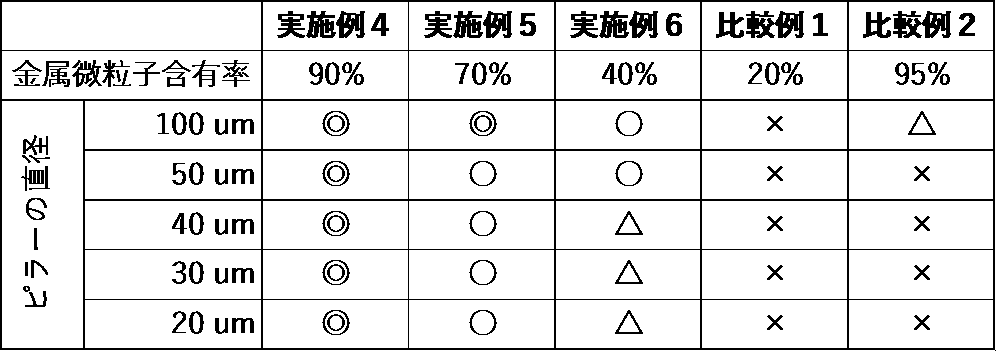
本結果は、金属微粒子含有率が40以上95質量%濃度未満の範囲内であれば、いずれの径においても導電性ピラーを作製可能であることを示している。
金属微粒子含有率が、40%未満である場合(例えば比較例1)には、その低い金属含有率により焼結後に導電性ピラーを形成することができないことが明らかとなった。
一方で、金属微粒子含有率が95%以上である場合(例えば比較例2)には、ペーストの粘度が高く、流動性が悪い。これにより、ゴムスキージを用いた場合には、開口部に導電ペーストが充填されないことが明らかとなった。
金属微粒子含有率が、40%未満である場合(例えば比較例1)には、その低い金属含有率により焼結後に導電性ピラーを形成することができないことが明らかとなった。
一方で、金属微粒子含有率が95%以上である場合(例えば比較例2)には、ペーストの粘度が高く、流動性が悪い。これにより、ゴムスキージを用いた場合には、開口部に導電ペーストが充填されないことが明らかとなった。
Claims (6)
- 金属微粒子と、
保護剤と、
を含有するピラー形成用導電ペーストであって、
前記金属微粒子の粒子径が1μm未満であり、かつ、前記導電ペースト中の金属微粒子含有率が40以上95質量%濃度未満であることを特徴とするピラー形成用導電ペースト。 - さらに沸点250℃以下の溶剤を含有することを特徴とする請求項1記載のピラー形成用導電ペースト。
- 請求項1記載の保護剤が炭素数8~200のポリエチレンオキシド構造を含む有機化合物を含有することを特徴とする請求項1又は2記載のピラー形成用導電ペースト。
- 請求項3記載の炭素数8~200のポリエチレンオキシド構造を含む有機化合物の含有率が全ペースト中15質量%濃度以下である、請求項1~3いずれか一項記載のピラー形成用導電ペースト。
- 請求項1記載の金属微粒子の金属が、銀、銅又はこれらの複合体である、請求項1~4いずれか一項記載のピラー形成用導電ペースト。
- 請求項1~5いずれか一項記載のピラー形成用導電ペーストを用いて作製されたピラー。
Priority Applications (3)
| Application Number | Priority Date | Filing Date | Title |
|---|---|---|---|
| CN201980039134.5A CN112272863A (zh) | 2018-06-27 | 2019-04-25 | 支柱形成用导电糊剂 |
| US15/733,948 US20210229172A1 (en) | 2018-06-27 | 2019-04-25 | Electrically conductive paste for forming pillars |
| KR1020207031556A KR20210023811A (ko) | 2018-06-27 | 2019-04-25 | 필러 형성용 도전 페이스트 |
Applications Claiming Priority (2)
| Application Number | Priority Date | Filing Date | Title |
|---|---|---|---|
| JP2018-121936 | 2018-06-27 | ||
| JP2018121936A JP2020004816A (ja) | 2018-06-27 | 2018-06-27 | ピラー形成用導電ペースト |
Publications (1)
| Publication Number | Publication Date |
|---|---|
| WO2020003725A1 true WO2020003725A1 (ja) | 2020-01-02 |
Family
ID=68984777
Family Applications (1)
| Application Number | Title | Priority Date | Filing Date |
|---|---|---|---|
| PCT/JP2019/017602 Ceased WO2020003725A1 (ja) | 2018-06-27 | 2019-04-25 | ピラー形成用導電ペースト |
Country Status (6)
| Country | Link |
|---|---|
| US (1) | US20210229172A1 (ja) |
| JP (1) | JP2020004816A (ja) |
| KR (1) | KR20210023811A (ja) |
| CN (1) | CN112272863A (ja) |
| TW (1) | TW202000806A (ja) |
| WO (1) | WO2020003725A1 (ja) |
Citations (1)
| Publication number | Priority date | Publication date | Assignee | Title |
|---|---|---|---|---|
| JP2014111800A (ja) * | 2012-12-05 | 2014-06-19 | Nippon Handa Kk | ペースト状金属微粒子組成物、固形状金属または固形状金属合金の製造方法、金属製部材の接合方法、プリント配線板の製造方法および電気回路接続用バンプの製造方法 |
Family Cites Families (3)
| Publication number | Priority date | Publication date | Assignee | Title |
|---|---|---|---|---|
| US8592995B2 (en) | 2009-07-02 | 2013-11-26 | Taiwan Semiconductor Manufacturing Company, Ltd. | Method and structure for adhesion of intermetallic compound (IMC) on Cu pillar bump |
| JP5672524B2 (ja) | 2010-07-02 | 2015-02-18 | 日立化成株式会社 | 半導体素子搭載用パッケージ基板の製造方法 |
| KR102344790B1 (ko) | 2014-08-29 | 2021-12-30 | 닛데쓰마이크로메탈가부시키가이샤 | 반도체 접속의 Cu 필러용 원기둥상 형성물 |
-
2018
- 2018-06-27 JP JP2018121936A patent/JP2020004816A/ja active Pending
-
2019
- 2019-04-25 KR KR1020207031556A patent/KR20210023811A/ko not_active Ceased
- 2019-04-25 CN CN201980039134.5A patent/CN112272863A/zh active Pending
- 2019-04-25 WO PCT/JP2019/017602 patent/WO2020003725A1/ja not_active Ceased
- 2019-04-25 US US15/733,948 patent/US20210229172A1/en not_active Abandoned
- 2019-05-10 TW TW108116154A patent/TW202000806A/zh unknown
Patent Citations (1)
| Publication number | Priority date | Publication date | Assignee | Title |
|---|---|---|---|---|
| JP2014111800A (ja) * | 2012-12-05 | 2014-06-19 | Nippon Handa Kk | ペースト状金属微粒子組成物、固形状金属または固形状金属合金の製造方法、金属製部材の接合方法、プリント配線板の製造方法および電気回路接続用バンプの製造方法 |
Also Published As
| Publication number | Publication date |
|---|---|
| TW202000806A (zh) | 2020-01-01 |
| JP2020004816A (ja) | 2020-01-09 |
| CN112272863A (zh) | 2021-01-26 |
| US20210229172A1 (en) | 2021-07-29 |
| KR20210023811A (ko) | 2021-03-04 |
Similar Documents
| Publication | Publication Date | Title |
|---|---|---|
| JP5190412B2 (ja) | 合金ナノ粒子及びその製造方法、並びにその合金ナノ粒子を用いたインク及びペースト | |
| JP5521207B2 (ja) | 導電膜形成用組成物及びその製造方法、並びに導電膜の形成方法 | |
| JP4047304B2 (ja) | 微粒銀粒子付着銀粉及びその微粒銀粒子付着銀粉の製造方法 | |
| US8337726B2 (en) | Fine particle dispersion and method for producing fine particle dispersion | |
| JP5306966B2 (ja) | 銅微粒子分散水溶液の製造方法、及び銅微粒子分散水溶液の保管方法 | |
| JP5377483B2 (ja) | 微小金属粒子含有組成物及びその製造方法 | |
| JP7434786B2 (ja) | 銅/酸化銅微粒子ペースト | |
| JP6016664B2 (ja) | 銅微粒子分散溶液、焼結導電体の製造方法、及び導電接続部材の製造方法 | |
| TWI780326B (zh) | 使用導電糊之導電柱之製造方法 | |
| JP5439827B2 (ja) | 銅微粒子分散体及びその製造方法 | |
| US20100178420A1 (en) | Method of preparing conductive ink composition for printed circuit board and method of producing printed circuit board | |
| JP2006328472A (ja) | 銀ナノ粒子の製造方法、銀ナノ粒子およびその用途 | |
| JP7453619B2 (ja) | 銅および酸化銅含有微粒子及びその製造方法 | |
| JP5063003B2 (ja) | 銅ナノ粒子の製造方法、銅ナノ粒子、導電性組成物および電子デバイス | |
| WO2020003725A1 (ja) | ピラー形成用導電ペースト | |
| US20140127409A1 (en) | Method for producing fine particle dispersion | |
| WO2016015382A1 (zh) | 导电墨水及其制备方法 | |
| JP2020102316A (ja) | ピラー用導電性ペースト | |
| JP7243827B2 (ja) | 導電性ピラー | |
| JP2008235035A (ja) | 金属ナノ粒子ペースト及び当該金属ナノ粒子ペーストの製造方法 | |
| JP4761110B2 (ja) | 金属被膜とその形成方法 | |
| KR101117694B1 (ko) | 전도성 나노 잉크 조성물 제조 방법 | |
| JP6722495B2 (ja) | 銀被覆銅粉およびその製造方法 |
Legal Events
| Date | Code | Title | Description |
|---|---|---|---|
| 121 | Ep: the epo has been informed by wipo that ep was designated in this application |
Ref document number: 19827261 Country of ref document: EP Kind code of ref document: A1 |
|
| NENP | Non-entry into the national phase |
Ref country code: DE |
|
| 122 | Ep: pct application non-entry in european phase |
Ref document number: 19827261 Country of ref document: EP Kind code of ref document: A1 |