WO2020003646A1 - 固体撮像素子、撮像装置、および、固体撮像素子の制御方法 - Google Patents
固体撮像素子、撮像装置、および、固体撮像素子の制御方法 Download PDFInfo
- Publication number
- WO2020003646A1 WO2020003646A1 PCT/JP2019/011034 JP2019011034W WO2020003646A1 WO 2020003646 A1 WO2020003646 A1 WO 2020003646A1 JP 2019011034 W JP2019011034 W JP 2019011034W WO 2020003646 A1 WO2020003646 A1 WO 2020003646A1
- Authority
- WO
- WIPO (PCT)
- Prior art keywords
- signal
- level
- pixels
- pixel
- pair
- Prior art date
- Legal status (The legal status is an assumption and is not a legal conclusion. Google has not performed a legal analysis and makes no representation as to the accuracy of the status listed.)
- Ceased
Links
Images















Classifications
-
- H—ELECTRICITY
- H04—ELECTRIC COMMUNICATION TECHNIQUE
- H04N—PICTORIAL COMMUNICATION, e.g. TELEVISION
- H04N25/00—Circuitry of solid-state image sensors [SSIS]; Control thereof
- H04N25/50—Control of the SSIS exposure
- H04N25/57—Control of the dynamic range
-
- H—ELECTRICITY
- H04—ELECTRIC COMMUNICATION TECHNIQUE
- H04N—PICTORIAL COMMUNICATION, e.g. TELEVISION
- H04N25/00—Circuitry of solid-state image sensors [SSIS]; Control thereof
- H04N25/50—Control of the SSIS exposure
- H04N25/57—Control of the dynamic range
- H04N25/58—Control of the dynamic range involving two or more exposures
- H04N25/587—Control of the dynamic range involving two or more exposures acquired sequentially, e.g. using the combination of odd and even image fields
-
- H—ELECTRICITY
- H04—ELECTRIC COMMUNICATION TECHNIQUE
- H04N—PICTORIAL COMMUNICATION, e.g. TELEVISION
- H04N25/00—Circuitry of solid-state image sensors [SSIS]; Control thereof
- H04N25/70—SSIS architectures; Circuits associated therewith
- H04N25/76—Addressed sensors, e.g. MOS or CMOS sensors
- H04N25/77—Pixel circuitry, e.g. memories, A/D converters, pixel amplifiers, shared circuits or shared components
-
- H—ELECTRICITY
- H04—ELECTRIC COMMUNICATION TECHNIQUE
- H04N—PICTORIAL COMMUNICATION, e.g. TELEVISION
- H04N25/00—Circuitry of solid-state image sensors [SSIS]; Control thereof
- H04N25/70—SSIS architectures; Circuits associated therewith
- H04N25/76—Addressed sensors, e.g. MOS or CMOS sensors
- H04N25/77—Pixel circuitry, e.g. memories, A/D converters, pixel amplifiers, shared circuits or shared components
- H04N25/778—Pixel circuitry, e.g. memories, A/D converters, pixel amplifiers, shared circuits or shared components comprising amplifiers shared between a plurality of pixels, i.e. at least one part of the amplifier must be on the sensor array itself
-
- H—ELECTRICITY
- H04—ELECTRIC COMMUNICATION TECHNIQUE
- H04N—PICTORIAL COMMUNICATION, e.g. TELEVISION
- H04N25/00—Circuitry of solid-state image sensors [SSIS]; Control thereof
- H04N25/70—SSIS architectures; Circuits associated therewith
- H04N25/76—Addressed sensors, e.g. MOS or CMOS sensors
- H04N25/78—Readout circuits for addressed sensors, e.g. output amplifiers or A/D converters
Definitions
- the present technology relates to a solid-state imaging device, an imaging device, and a method for controlling the solid-state imaging device. More specifically, the present invention relates to a solid-state imaging device that differentially amplifies pixel signals, an imaging device, and a method for controlling the solid-state imaging device.
- a solid-state imaging device has been used for capturing image data in an imaging device or the like. If the sensitivity of each pixel of the solid-state imaging device is relatively low, when the amount of ambient light is relatively small, image data may be entirely dark and image quality may be degraded. Therefore, in order to increase the sensitivity, for example, a solid-state imaging device has been proposed in which a current mirror circuit is connected to a pair of pixels and a differential amplifier circuit including the pixels and the current mirror circuit is configured (for example, See Patent Document 1.).
- the differential amplifier circuit differentially amplifies the respective signals of the pair of pixels, so that the sensitivity of the pixels can be made higher than when the current mirror circuit is not connected.
- the dynamic range may be insufficient and image quality may be degraded. If a plurality of pieces of image data (frames) having different exposure times are imaged and synthesized, a synthesized frame having a wide dynamic range can be obtained, but the frame rate is reduced instead.
- the frame rate of the synthesized frame is reduced to 30 Hertz (Hz).
- the above-described solid-state imaging device has a problem that the dynamic range of image data cannot be widened without lowering the frame rate.
- the present technology has been created in view of such a situation, and has an object to broaden a dynamic range without lowering a frame rate in a solid-state imaging device provided with a differential amplifier circuit.
- a first aspect of the present technology is a process of outputting a differentially amplified signal obtained by amplifying a difference between generated voltages of a pair of pixels and a process of outputting the differentially amplified signal.
- a readout circuit that performs a process of outputting a pixel signal of the generated voltage of at least one of the pixels each time the pair of pixels is exposed, and the output differential amplified signal and the output pixel signal.
- a solid-state imaging device including a processing unit that performs a combining process for combining, and a control method thereof. This brings about an effect that the dynamic range is expanded by combining the differential amplified signal and the image signal.
- each of the pair of pixels may generate a reset level as the generated voltage when initialized, and generate a signal level as the generated voltage when exposure is completed. Good. This brings about an effect that the dynamic range is expanded by combining the signals obtained from the reset level and the signal level.
- the readout circuit may include a first reset level obtained by differentially amplifying the reset level of each of the pair of pixels and a second reset level that is the reset level of any of the pair of pixels. And outputting a first signal level obtained by differentially amplifying the signal level of each of the pair of pixels and a second signal level which is the signal level of one of the pair of pixels. You may. This brings about an effect that a dynamic range is expanded by combining signals obtained from at least one of the first reset level and the second reset level and the first signal level and the second signal level.
- the readout circuit may output the first signal level and the second signal level after outputting the first reset level and the second reset level. This brings about an effect that the dynamic range is expanded by combining the signals obtained from the first reset level, the second reset level, the first signal level, and the second signal level.
- the readout circuit may further output the second signal level and the second reset level after outputting the first reset level and the first signal level. This brings about an effect that the dynamic range is expanded by combining the first reset level, the first signal level, the second signal level, and the signal obtained from the second reset level.
- the processing unit sequentially converts the first reset level, the first signal level, the second signal level, and the second reset level into digital signals. And converting the first reset level and the first signal level into a digital signal in order when the illuminance is less than the predetermined value, and performing the synthesizing process based on the digital signal. And a synthesizing processing unit for performing the processing. Thereby, when the illuminance is less than the predetermined value, the conversion of the second signal level and the second reset level is stopped.
- the processing section selects and outputs the differential amplified signal when the illuminance is less than a predetermined value, and outputs the pixel signal when the illuminance exceeds the predetermined value. May be selected and output. This brings about an effect that a signal corresponding to the illuminance is selected.
- the readout circuit may output one of the first signal level and the second signal level after outputting the first reset level and the second reset level. This brings about an effect that conversion of one of the first signal level and the second signal level becomes unnecessary.
- the readout circuit includes a plurality of unit readout circuits each including a current mirror circuit, a current source, and a switch arranged in a predetermined direction, and the switch includes a plurality of unit readout circuits of the plurality of unit readout circuits.
- the respective current mirror circuits and the current sources may be connected to each other. This brings about an effect that the current mirror circuit and the current source are horizontally connected.
- the first aspect may further include a pixel array unit in which a plurality of pixels are arranged in a two-dimensional lattice, and the pair of pixels may be arranged in the pixel array unit in a horizontal direction. This brings about the effect that the differential amplified signal is read out from the pair of pixels arranged horizontally.
- the first side surface may further include a pixel array unit in which a plurality of pixels are arranged in a two-dimensional lattice, and the pair of pixels may be arranged in the pixel array unit in a vertical direction. This brings about an effect that the differential amplified signal is read from a pair of pixels arranged in the vertical direction.
- the image processing apparatus further includes a pixel array unit in which a plurality of pixels each assigned a vertical address and a horizontal address are arranged in a two-dimensional lattice.
- both the vertical address and the horizontal address may be different pixels. This brings about the effect that the differentially amplified signal is read out from the pair of pixels arranged diagonally.
- the first aspect further includes a pixel array unit in which a plurality of readout pixels and reference pixels associated with the plurality of readout pixels are arranged, and one of the pair of pixels includes the plurality of readout pixels.
- One of the readout pixels, and the other of the pair of pixels is the reference pixel, and the readout circuit outputs a differential amplified signal obtained by amplifying a difference between a pixel signal of each of the readout pixel and the reference pixel. And outputting the pixel signal of the readout pixel. This brings about an effect that the differential amplified signal is read from the read pixel and the reference pixel.
- the read circuit may include a current mirror circuit. This brings about an effect that a differential amplified signal is read from a pair of pixels to which the current mirror circuit is connected.
- the current mirror circuit may be a cascode current mirror circuit. This brings about the effect that the differentially amplified signal is read from a pair of pixels to which the cascode current mirror circuit is connected.
- the current mirror circuit is connected to a pair of vertical signal lines
- the readout circuit further includes a switch for selecting one of the pair of vertical signal lines and connecting to the processing unit. May be provided. This brings about the effect that the differential amplified signal or the pixel signal is read from one of the pair of vertical signal lines.
- a digital-to-analog converter including a current source for generating a predetermined reference current and a resistor for generating a predetermined reference signal corresponding to the reference current, and controlling a value of the reference current
- the processing unit may further include a system control unit, and the processing unit may include a comparator that compares the signal output by the readout circuit with a predetermined reference signal. This brings about an effect that power consumption is reduced by controlling the reference current.
- a process of outputting a pair of pixels and a differentially amplified signal obtained by amplifying a difference between respective generated voltages of the pair of pixels and a method of outputting the generated voltage of at least one of the pair of pixels
- a readout circuit that performs the process of outputting the pixel signal of each time the pair of pixels are exposed, and a processing unit that performs a combining process of combining the output differential amplified signal and the output pixel signal. It is an imaging device provided with. The dynamic range is expanded by combining the differentially amplified signal and the image signal from the pair of pixels.
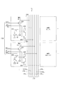
- FIG. 1 is a block diagram illustrating a configuration example of a solid-state imaging device according to a first embodiment of the present technology.
- FIG. 2 is a block diagram illustrating a configuration example of a pixel circuit according to the first embodiment of the present technology.
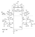
- FIG. 2 is a circuit diagram illustrating a configuration example of a column readout circuit unit according to the first embodiment of the present technology.
- FIG. 2 is a circuit diagram illustrating a configuration example of a unit readout circuit according to the first embodiment of the present technology.
- FIG. 2 is a circuit diagram illustrating a configuration example of a differential amplifier circuit including a unit readout circuit and a pixel according to the first embodiment of the present technology.
- FIG. 2 is a block diagram illustrating a configuration example of a column signal processing unit according to the first embodiment of the present technology.
- FIG. 2 is a circuit diagram illustrating a configuration example of an ADC (Analog to Digital Converter) according to the first embodiment of the present technology.
- FIG. 2 is a circuit diagram illustrating a configuration example of a synthesis processing unit according to the first embodiment of the present technology.
- 6 is a graph illustrating an example of a relationship between an incident light amount and a level of a pixel signal according to the first embodiment of the present technology.
- 5 is a timing chart illustrating an example of differential reading according to the first embodiment of the present technology.
- 5 is a timing chart illustrating an example of SF (Source / Follower) reading in the first embodiment of the present technology.
- FIG. 5 is a timing chart illustrating an example of control for reading out a pixel signal according to the first embodiment of the present technology.
- FIG. 7 is a diagram illustrating an example of an operation of a column readout circuit unit and a column signal processing unit according to the first embodiment of the present technology and a comparative example.
- 5 is a flowchart illustrating an example of an operation of the solid-state imaging device according to the first embodiment of the present technology.
- FIG. 11 is a circuit diagram illustrating a configuration example of a unit readout circuit according to a second embodiment of the present technology.
- 13 is a timing chart illustrating an example of differential reading according to the second embodiment of the present technology.
- 15 is a timing chart illustrating an example of SF reading according to the second embodiment of the present technology.
- FIG. 11 is a circuit diagram illustrating a configuration example of a unit readout circuit according to a second embodiment of the present technology.
- 13 is a timing chart illustrating an example of differential reading according to the second embodiment of the present
- 14 is a circuit diagram illustrating a configuration example of an ADC and a synthesis processing unit according to a third embodiment of the present technology.
- 13 is a timing chart illustrating an example of an operation of the solid-state imaging device according to the third embodiment of the present technology.
- 15 is a timing chart illustrating an example of an operation of a solid-state imaging device according to a modification example of the third embodiment of the present technology.
- 15 is a timing chart illustrating an example of an operation of the solid-state imaging device at low illuminance according to the fourth embodiment of the present technology.
- 15 is a timing chart illustrating an example of an operation of a solid-state imaging device at high illuminance according to a fifth embodiment of the present technology.
- FIG. 21 is a circuit diagram illustrating a configuration example of a differential amplifier circuit according to a seventh embodiment of the present technology.
- FIG. 21 is a circuit diagram illustrating a configuration example of a differential amplifier circuit according to an eighth embodiment of the present technology.
- 21 is a timing chart illustrating an example of an operation of a solid-state imaging device according to an eighth embodiment of the present technology.
- FIG. 21 is a block diagram illustrating a configuration example of a solid-state imaging device according to a ninth embodiment of the present technology.
- FIG. 28 is a circuit diagram illustrating a configuration example of a DAC (Digital to Analog) and a comparator according to a ninth embodiment of the present technology.
- FIG. 2 is a block diagram illustrating a schematic configuration example of a vehicle control system.
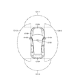
- FIG. 4 is an explanatory diagram illustrating an example of an installation position of an imaging unit.
- FIG. 1 is a block diagram illustrating a configuration example of a solid-state imaging device 10 according to the first embodiment of the present technology.
- the solid-state imaging device 10 includes a pixel array unit 11, a vertical drive unit 12, a column readout circuit unit 13, a column signal processing unit 14, a horizontal drive unit 15, a system control unit 16, a signal processing unit 17, and a data storage unit 18. It is comprised including.
- the circuits such as the pixel array unit 11 and the like are formed on a plurality of the same or electrically connected laminated semiconductor substrates (chips).
- the pixel array unit 11 includes a unit pixel (hereinafter, referred to as an effective unit pixel) having a photoelectric conversion element capable of photoelectrically converting a charge amount according to an incident light amount, storing the charge amount therein, and outputting the signal as a signal. They are two-dimensionally arranged in a matrix.
- the pixel array unit 11 may include a region in which dummy unit pixels and light-shielding unit pixels are two-dimensionally arranged in a matrix in addition to the effective unit pixels.
- the dummy unit pixel is a pixel having a structure without a photodiode for performing photoelectric conversion
- the light-shielding unit pixel is a pixel equivalent to an effective pixel except that the light receiving surface is shielded to block external light incidence. It is.
- the photocharge having a charge amount corresponding to the incident light amount may be simply described as “charge”, and the unit pixel may be simply described as “pixel”.
- a pixel drive line 31 is further formed for each row in the matrix pixel array along the left-right direction in the drawing (pixel array direction of the pixel row), and a vertical pixel wiring 32 is provided for each column. Are formed along the vertical direction in the figure (the arrangement direction of the pixels in the pixel column).
- One end of the pixel drive line 31 is connected to an output end corresponding to each row of the vertical drive unit 12.
- the column readout circuit section 13 includes at least a circuit for supplying a constant current for each column in a pixel in a selected row of the pixel array section 11, a current mirror circuit forming a high gain amplifier, and a readout mode switch. These constitute an amplifier together with the transistors in the selected pixel of the pixel array unit 11. This amplifier converts a photocharge signal into a voltage signal and outputs the voltage signal to the vertical pixel wiring 32. Note that the column readout circuit unit 13 is an example of a readout circuit described in the claims.
- the vertical drive unit 12 is a pixel drive unit that includes a shift register, an address decoder, and the like, and drives each pixel of the pixel array unit 11 simultaneously for all pixels or in units of rows. Although the specific configuration of the vertical drive unit 12 is not shown, the vertical drive unit 12 has a configuration including a read-out scanning system and a sweep-out scanning system, or batch sweeping and batch transfer.
- the readout scanning system selectively scans the unit pixels in the pixel array unit in order of rows in order to read out signals from the unit pixels.
- the sweeping scan is performed for the readout row on which the readout scanning is performed by the readout scanning system by a time corresponding to the shutter speed before the readout scanning.
- global exposure global shutter operation
- batch sweeping is performed ahead of batch transfer by the shutter speed time.
- the electronic shutter operation refers to an operation of discarding unnecessary photocharges accumulated in the photoelectric conversion element until immediately before and newly starting exposure (starting accumulation of photocharges).
- the signal read out by the readout operation by the readout scanning system corresponds to the amount of light incident after the immediately preceding readout operation or the electronic shutter operation.
- the period from the readout timing by the immediately preceding readout operation or the sweep timing by the electronic shutter operation to the readout timing by the current readout operation is the photocharge accumulation time (exposure time) in the unit pixel.
- the time from batch sweep to batch transfer is the accumulation time (exposure time).
- the pixel signal output from each unit pixel of the pixel row selectively scanned by the vertical driving unit 12 is supplied to the column signal processing unit 14 through each of the vertical pixel wirings 32.
- the column signal processing unit 14 performs predetermined signal processing on a pixel signal output from each unit pixel in the selected row through the vertical pixel wiring 32 for each pixel column of the pixel array unit, and performs pixel processing after the signal processing. Temporarily.
- the column signal processing unit 14 performs at least noise removal processing, for example, CDS (Correlated Double Sampling) processing as signal processing.
- CDS Correlated Double Sampling
- the column signal processing unit may be provided with, for example, an AD (Analog-Digital) conversion function in addition to the noise removal processing, and output the signal level as a digital signal.
- AD Analog-Digital
- the horizontal drive unit 15 is configured by a shift register, an address decoder, and the like, and sequentially selects unit circuits corresponding to the pixel columns of the column signal processing unit 14.
- the pixel signals subjected to the signal processing by the column signal processing unit 14 are sequentially output to the signal processing unit 17 by the selective scanning by the horizontal driving unit 15.
- the system control unit 16 includes a timing generator that generates various timing signals.
- the system control unit 16 controls driving of the vertical driving unit 12, the column readout circuit unit 13, the column signal processing unit 14, the horizontal driving unit 15, and the like based on various timing signals generated by the timing generator.
- the solid-state imaging device 10 further includes a signal processing unit 17 and a data storage unit 18.
- the signal processing unit 17 has at least an addition processing function, and performs various signal processing such as addition processing on the pixel signal output from the column signal processing unit 14.
- the data storage unit 18 temporarily stores data necessary for the signal processing in the signal processing unit 17.
- the signal processing unit 17 and the data storage unit 18 may be processed by an external signal processing unit provided on a substrate different from the solid-state imaging device 10, for example, a DSP (Digital Signal Processor) or software. Alternatively, they may be mounted on the same substrate as the solid-state imaging device 10.
- DSP Digital Signal Processor
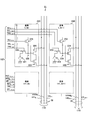
- FIG. 2 is a circuit diagram illustrating a configuration example of the pixels 220 and 230 according to the first embodiment of the present technology.
- a plurality of pixels such as the pixels 220 and 230 are arranged in a two-dimensional lattice.
- the pixel 220 is a pixel adjacent to the pixel 230.
- the pixels 220 are arranged in 2k (k is an integer) columns which are even columns, and the pixels 230 are arranged in 2k + 1 columns which are odd columns.
- the pixel 220 includes a photodiode 221, a transfer transistor 222, a floating diffusion region 226, a reset transistor 223, an amplification transistor 224, and a selection transistor 225.
- MOS Metal-Oxide-Semiconductor
- a pixel drive line 31 having one end connected to the vertical drive section 12 is wired for each row along the horizontal direction.
- Each row of pixel drive lines 31 includes six signal lines. These signal lines transmit six drive signals.
- a vertical pixel wiring 32 In the pixel array section 11, a vertical pixel wiring 32, one end of which is connected to the column readout circuit section 13, is wired for each column along the vertical direction.
- Each of the even-numbered column vertical pixel wirings 32 includes a vertical signal line VSL 2k , a vertical reset input line VRD 2k, and a vertical current supply line VCOM 2k .
- the odd-numbered vertical pixel lines 32 include a vertical signal line VSL 2k + 1 , a vertical reset input line VRD 2k + 1, and a vertical current supply line VCOM 2k + 1 .
- the number of columns is J (J is an integer)
- the number of wirings in the vertical direction is 3 ⁇ J.
- the anode of the photodiode 221 is grounded, and the cathode of the photodiode 221 is connected to the source of the transfer transistor 222.
- the drain of the transfer transistor 222 is connected to the source of the reset transistor 223 and the gate of the amplification transistor 224. This connection point constitutes the floating diffusion region 226.
- the drain of the reset transistor 223 is connected to the vertical reset input line VRD 2k .
- the source of the amplification transistor 224 is connected to the vertical current supply line VCOM 2k .
- the drain of the amplifying transistor 224 is connected to the source of the selection transistor 225, the drain of the selection transistor 225 is connected to the vertical signal line VSL 2k.
- the gates of the transfer transistor 222, the reset transistor 223, and the selection transistor 225 are connected to the vertical drive unit 12 via the pixel drive lines 31, respectively. A pulse as a drive signal is supplied to each of these transistors.
- the pixel 230 includes a photodiode 231, a transfer transistor 232, a floating diffusion region 236, a reset transistor 233, an amplification transistor 234, and a selection transistor 235.
- the connection configuration of these elements is similar to that of the pixel 220.
- the configuration of the pixels in the even columns other than the pixel 220 is the same as that of the pixel 220, and the configuration of the pixels in the odd columns other than the pixel 230 is the same as the pixel 230. That is, the even columns are connected to the vertical signal line VSL 2k , and the odd columns are connected to the vertical signal line VSL 2k + 1 .
- the reset transistor 223 turns on and off the discharge of the charge accumulated in the floating diffusion region 226 according to the drive signal RST (i, 2k) supplied from the vertical drive unit 12.
- the number of rows is I (I is an integer), and the subscript i is an integer from 0 to I.
- the reset transistor 223 discharges (resets) the charge accumulated in the floating diffusion region 226.
- the floating diffusion region 226 is electrically disconnected from the vertical reset input line VRD 2k to be in a floating state.
- the photodiode 221 photoelectrically converts incident light, and generates and accumulates charges corresponding to the amount of light.
- the transfer transistor 222 turns on and off the transfer of charges from the photodiode 221 to the floating diffusion region 226 according to the drive signal TRG (i, 2k) supplied from the vertical drive unit 12. For example, when the high-level drive signal TRG (i, 2k) is supplied, the transfer transistor 222 transfers the charge accumulated in the photodiode 221 to the floating diffusion region 226, and the low-level drive signal TRG (i , 2k), the transfer of charges is stopped. Note that while the transfer transistor 222 stops transferring charges to the floating diffusion region 226, the charges that have been photoelectrically converted are accumulated in the photodiode 221.
- the floating diffusion region 226 has a function of accumulating charges transferred from the photodiode 221 via the transfer transistor 222. In the floating state where the reset transistor 223 is turned off, the potential of the floating diffusion region 226 is modulated in accordance with the accumulated charge amount.
- the amplifying transistor 224 functions as an amplifier using the potential fluctuation of the floating diffusion region 226 connected to its gate as an input signal, and the output voltage signal is output to the vertical signal line VSL 2k via the selection transistor 225.
- the selection transistor 225 turns on and off the output of the voltage signal from the amplification transistor 224 to the vertical signal line VSL 2k according to the drive signal SEL (i, 2k) supplied from the vertical drive unit 12. For example, when the high-level drive signal SEL (i, 2k) is supplied, the selection transistor 225 outputs a voltage signal to the vertical signal line VSL 2k , and the low-level drive signal SEL (i, 2k) is supplied. Then, the output of the voltage signal is stopped. This makes it possible to extract only the output of the selected pixel from the vertical signal line to which a plurality of pixels are connected.
- drive signals RST (i, 2k + 1) , TRG (i, 2k + 1), and SEL (i, 2k + 1) are supplied to the transistors in the pixel 230, and the same as the corresponding transistors in the pixel 220 according to the drive signals.
- drive signals RST (i, 2k + 1) , TRG (i, 2k + 1), and SEL (i, 2k + 1) are supplied to the transistors in the pixel 230, and the same as the corresponding transistors in the pixel 220 according to the drive signals.
- FIG. 3 is a block diagram illustrating a configuration example of the column readout circuit unit 13 according to the first embodiment of the present technology.
- unit readout circuits 300 are arranged every two columns. Assuming that the number of columns is J, J / 2 unit readout circuits 300 are arranged.
- Each unit readout circuit 300 is connected to the pixel array unit 11 via vertical signal lines VSL 2k and VSL 2k + 1 , vertical reset input lines VRD 2k and VRD 2k + 1 , and vertical current supply lines VCOM 2k and VCOM 2k + 1. I have.
- the unit readout circuit 300 supplies voltage signals from the vertical signal lines VSL 2k and VSL 2k + 1 to the column signal processing unit 14 as pixel signals Vout 2k and Vout2 k + 1 .
- FIG. 4 is a circuit diagram illustrating a configuration example of the unit readout circuit 300 according to the first embodiment of the present technology.
- the unit read circuit 300 includes P-type transistors 311 and 312, switches 313 and 314, switches 316 to 329, and current sources 331 and 332.
- P-type transistors 311 and 312 for example, MOS transistors are used.
- P-type transistors 311 and 312 are connected in parallel to the terminal of power supply voltage VDD, and their gates are connected.
- the switch 313 short-circuits the gate and the drain of the P-type transistor 311 according to the drive signal DAS1 from the system control unit 16. For example, when the drive signal DAS1 is at a high level, the switch 313 shifts to the ON state, and the gate and the drain of the P-type transistor 311 are short-circuited.
- the switch 314 short-circuits the gate and the drain of the P-type transistor 312 according to the drive signal DAS2 from the system control unit 16. For example, when the drive signal DAS2 is at a high level, the switch 314 is turned on, and the gate and the drain of the P-type transistor 312 are short-circuited.
- the P-type transistors 311 and 312 function as a current mirror circuit.
- the switch 316 connects the terminal of the power supply voltage VDD to the vertical reset input line VRD 2k according to the drive signal SFEN from the system control unit 16.
- the drive signal SFEN is the case of high level
- the power supply voltage VDD is connected to the vertical reset input line VRD 2k.
- the switch 317 connects a terminal of a reset voltage Vrst different from the power supply voltage VDD to the vertical reset input line VRD 2k according to the drive signal DAS1 from the system control unit 16.
- the drive signal DAS1 is the case of high level
- the reset voltage Vrst is connected to the vertical reset input line VRD 2k.
- the reset voltage Vrst a voltage lower than the power supply voltage VDD is applied as the reset voltage Vrst.
- the power supply voltage VDD is 3.3 volts (V)
- the reset voltage Vrst is 2.2 volts (V).
- the higher the reset voltage Vrst the more advantageous the charge transfer is, and can transfer a lot of signal charges.
- the lower the reset voltage Vrst the larger the amplitude of the output voltage.
- the switch 318 connects the P-type transistor 311 to the vertical reset input line VRD 2k according to the drive signal DAS2 from the system control unit 16.
- the drive signal DAS2 is P-type transistor 311 is connected to a vertical reset input line VRD 2k in the case of a high level.
- the switch 319 connects the P-type transistor 311 to the vertical signal line VSL 2k according to the drive signal DAEN from the system control unit 16. For example, when the drive signal DAEN is at a high level, the P-type transistor 311 is connected to the vertical signal line VSL 2k .
- the switch 320 connects the terminal of the power supply voltage VDD to the vertical current supply line VCOM 2k according to the drive signal SFEN from the system control unit 16. For example, when the drive signal SFEN is at a high level, the power supply voltage VDD is connected to the vertical current supply line VCOM 2k .
- the switch 321 connects the terminal of the power supply voltage VDD to the vertical reset input line VRD 2k + 1 according to the drive signal SFEN from the system control unit 16. For example, when the drive signal SFEN is at a high level, the power supply voltage VDD is connected to the vertical reset input line VRD 2k + 1 .
- the switch 322 connects the terminal of the reset voltage Vrst to the vertical reset input line VRD 2k + 1 according to the drive signal DAS2 from the system control unit 16. For example, when the drive signal DAS2 is at a high level, the reset voltage Vrst is connected to the vertical reset input line VRD 2k + 1 .
- the switch 323 connects the P-type transistor 312 to the vertical reset input line VRD 2k + 1 according to the drive signal DAS1 from the system control unit 16. For example, when the drive signal DAS1 is at a high level, the P-type transistor 312 is connected to the vertical reset input line VRD 2k + 1 .
- the switch 324 connects the P-type transistor 312 to the vertical signal line VSL 2k + 1 according to the drive signal DAEN from the system control unit 16. For example, when the driving signal DAEN is at a high level, the P-type transistor 312 is connected to the vertical signal line VSL 2k + 1 .
- the switch 325 connects the terminal of the power supply voltage VDD to the vertical current supply line VCOM 2k + 1 according to the drive signal SFEN from the system control unit 16. For example, when the drive signal SFEN is at a high level, the power supply voltage VDD is connected to the vertical current supply line VCOM 2k + 1 .
- the switch 326 connects the vertical current supply line VCOM 2k to the current source 331 according to the drive signal DAEN from the system control unit 16. For example, when the drive signal DAEN is at a high level, the vertical current supply line VCOM 2k is connected to the current source 331.
- the switch 327 connects the vertical signal line VSL 2k to the current source 331 according to the drive signal SFEN from the system control unit 16. For example, when the drive signal SFEN is at a high level, the vertical signal line VSL 2k is connected to the current source 331.
- the switch 328 connects the vertical current supply line VCOM 2k + 1 to the current source 332 according to the drive signal DAEN from the system control unit 16. For example, when the drive signal DAEN is at a high level, the vertical current supply line VCOM 2k + 1 is connected to the current source 332.
- the switch 329 connects the vertical signal line VSL 2k + 1 to the current source 332 in accordance with the drive signal SFEN from the system control unit 16. For example, when the drive signal SFEN is at a high level, the vertical signal line VSL 2k + 1 is connected to the current source 332.
- the unit readout circuit 300 and the pixels 220 and 230 form a differential amplifier circuit by the low-level drive signal SFEN and the high-level drive signal DAEN.
- the operation of reading the differential amplified signal from the differential amplifier circuit is called "differential read”.
- a mode in which only the differential reading is performed in the 1 V period which is the period of the vertical synchronization signal is hereinafter referred to as a “differential mode”.
- the unit readout circuit 300 and the pixels 220 and 230 form a source follower circuit by the high-level drive signal SFEN and the low-level drive signal DAEN.
- the operation of reading a pixel signal from this source follower circuit is referred to as “SF (Source @ Follower) reading”.
- SF mode A mode in which only SF reading is performed in the 1 V period is hereinafter referred to as an “SF mode”.
- the conversion efficiency can be greatly increased by increasing the gain for the image signal, but the operating point is narrow and it is difficult to expand the dynamic range.
- the differential mode since the image signal can be amplified with a relatively high gain, the differential mode is suitable for imaging in a dark place.
- the image signal in the SF mode, the image signal can be amplified only with a relatively low gain, but the dynamic range can be relatively widened, so that it is suitable for imaging in a bright place. For this reason, for example, the differential mode is set when the amount of ambient light is smaller than a predetermined threshold, and the SF mode is set when the amount of light is equal to or greater than the threshold.
- the differential mode a pair of pixels arranged in the vertical direction is selected, one of which is selected as a “read pixel” and the other is selected as a “reference pixel”.
- the readout pixel is a pixel from which a voltage corresponding to the amount of the photoelectrically converted charge is read out as a signal voltage.
- the reference pixel is a voltage in which the voltage of the floating diffusion region has been initialized to a predetermined reference voltage. In the differential mode, a signal obtained by amplifying the difference between the signal voltage and the reference voltage is read.
- the readout pixel and the reference pixel can be switched by controlling the drive signals DAS1 and DAS2. For example, when only the drive signal DAS1 of the drive signals DAS1 and DAS2 is set to the high level, one of the pixels 220 and 230 becomes a readout pixel. Conversely, when only the drive signal DAS2 is set to the high level, the pixels 220 and 230 The other is a readout pixel.
- both the differential read and the SF read can be performed within the 1 V period. Since this mode is used to perform high dynamic range synthesis, this mode is hereinafter referred to as “HDR (High Dynamic Dynamic Range) mode”.
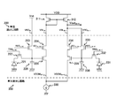
- FIG. 5 is a circuit diagram illustrating a configuration example of a differential amplifier circuit including the unit readout circuit 300 and the pixels 220 and 230 according to the first embodiment of the present technology.
- This differential amplifier circuit includes a read pixel to be read, a reference pixel that applies a reference voltage, a current mirror circuit arranged in the column read circuit unit 13, and a current source 330.
- the pixel 220 is used as a reference pixel
- the pixel 230 is used as a readout pixel.
- the current source 330 is an element in which the current sources 331 and 332 are combined into one for convenience of description. It should be noted that, in the figure, a switch group is omitted for convenience of description.
- the vertical reset input line VRD 2k is connected to a predetermined reset voltage Vrst in the unit read circuit 300 in the column read circuit section 13. At the time of reset, a desired input voltage signal is applied to the floating diffusion region 226 of the selected reference pixel, that is, the input terminal of the reference-side amplification transistor 224 through this wiring.
- the vertical signal line VSL 2k on the reference side is connected to the drain and gate of the P-type transistor 311 and the gate of the P-type transistor 312 of the current mirror circuit in the column readout circuit unit 13.
- the read-side vertical signal line VSL 2k + 1 is connected to the drain of the P-type transistor 312 in the column read-out circuit unit 13 and the floating diffusion region 236 of the read-out pixel (that is, the input terminal of the read-side amplification transistor 234) by the reset transistor 233. Connected via Thus, the output signal of the differential amplifier circuit is negatively fed back. The output signal of the differential amplifier circuit is taken out from the vertical signal line VSL 2k + 1 . Further, the vertical current supply lines VCOM 2k and VCOM 2k + 1 on the reference side and the read side are connected to the current source 330.
- the reset transistor 223 When the reference pixel (here, pixel 220) generates the reference voltage, the reset transistor 223 is turned on, and supplies the reset voltage Vrst to the floating diffusion region 226.
- the read pixel here, the pixel 230
- the reset transistor 233 when reading the signal voltage, the reset transistor 233 is turned on immediately before the transfer, and a voltage different from the reset voltage Vrst according to the power supply voltage VDD is supplied via the current mirror circuit.
- the floating diffusion region 236 is supplied. Then, charges are transferred from the photodiode 231 in the read pixel, and a signal voltage is generated.
- a signal obtained by amplifying the difference between the reference voltage and the signal voltage is read as the pixel signal Vout 2k + 1 .
- the positional relationship between the reference pixel and the readout pixel is not fixed, and can be interchanged as described above. For example, after the pixel 220 is selected as the reference pixel and the pixel 230 as the readout pixel, the pixel 220 is then selected as the readout pixel and the pixel 230 as the reference pixel.
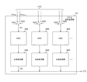
- FIG. 6 is a block diagram illustrating a configuration example of the column signal processing unit 14 according to the first embodiment of the present technology.
- the column signal processing unit 14 includes a switch 410, an ADC 420, and a synthesis processing unit 430 for every two columns.
- the switch 410 selects one of the pixel signals Vout 2k and Vout 2k + 1 from the corresponding two columns in the pixel array unit 11 in accordance with the drive signal DAS1, and supplies the analog signal Ain to the ADC 420.
- the ADC 420 converts the analog signal Ain into a digital signal.
- the ADC 420 supplies the digital signal to the synthesis processing unit 430.
- the combining processing unit 430 performs HDR combining processing for widening the dynamic range of the digital signal from the ADC 420 in the HDR mode. On the other hand, in the differential mode and the SF mode, the HDR combining processing is not executed.
- the synthesis processing unit 430 outputs the pixel data SIG after the HDR synthesis processing to the signal processing unit 17.
- FIG. 7 is a circuit diagram illustrating a configuration example of the ADC 420 according to the first embodiment of the present technology.
- the ADC 420 includes a comparator 520, a switch 423, and counters 421 and 422.
- the comparator 520 compares the reference signal V slope whose level changes like a slope with the analog signal Ain. It is assumed that the amplitude range of the reference signal V slope at the time of differential reading is the same as that at the time of SF reading. The comparator 520 supplies the comparison result to the counters 421 and 422.
- the switch 423 short-circuits the output terminal of the comparator 520 and the input terminal on the analog signal Ain side according to the drive signal AZ for auto-zero from the system control unit 16.
- the counters 421 and 422 count the count value within a period until the comparison result is inverted under the control of the system control unit 16.
- the system control unit 16 controls the counter 422 to count the difference between the P-phase level and the D-phase level from the source follower circuit.
- the P-phase level is a voltage (level) of a pixel signal Vout 2k or Vout 2k + 1 generated by the pixel 220 or 230 when the floating diffusion region is initialized.
- the D-phase level is a voltage (level) of a pixel signal Vout 2k or Vout 2k + 1 generated by the pixel 220 or 230 when the exposure of the pixel 220 or 230 is completed.
- P2 level and the D-phase level of the source follower circuit are referred to as “P2 level” and “D2 level”.
- the P-phase level and the D-phase level are examples of the generated voltage described in the claims.
- the P2 level is an example of a second reset level described in the claims
- the D2 level is an example of a second signal level described in the claims.
- the system control unit 16 controls the counter 421 to count the difference between the P-phase level and the D-phase level from the differential amplifier circuit.
- the P-phase level from the differential amplifier circuit is the level of a differentially amplified signal obtained by amplifying the difference between the P-phase level of the read pixel and the P-phase level of the reference pixel.
- the D-phase level from the differential amplifier circuit is a level of a differential amplification signal obtained by amplifying a difference between the D-phase level of the readout pixel and the D-phase level of the reference pixel.
- P1 level and the D-phase level of the differential amplifier circuit are referred to as “P1 level” and “D1 level”.
- the P1 level and the D1 level are examples of the differentially amplified signal described in the claims.
- the P1 level is an example of a first reset level described in the appended claims
- the D1 level is an example of a first signal level described in the appended claims.
- the counter 421 outputs a digital signal indicating a difference between the P1 level and the D1 level to the synthesis processing unit 430 as a digital signal Dout1.
- the counter 422 outputs a digital signal indicating a difference between the P2 level and the D2 level to the synthesis processing unit 430 as a digital signal Dout2.
- the processing for obtaining these differences corresponds to the CDS processing.
- FIG. 8 is a circuit diagram illustrating a configuration example of the synthesis processing unit 430 according to the first embodiment of the present technology.
- the synthesis processing unit 430 includes a multiplier 431, a determination circuit 432, and a switch 433.
- the multiplier 431 multiplies the digital signal Dout2 indicating the difference between the P2 level and the D2 level by a predetermined coefficient A, and outputs a result of the multiplication to the determination circuit 432.
- the coefficient A for example, a value represented by the following equation is set.
- ⁇ D is the conversion efficiency at the time of differential reading
- G AD is the analog gain at the time of differential reading
- ⁇ S is the conversion efficiency at the time of SF reading
- G AS is the analog gain at the time of SF reading.
- the determination circuit 432 determines whether the multiplication result is larger than a predetermined threshold. The determination circuit 432 supplies the determination result to the switch 433.
- the switch 433 selects one of the digital signal Dout1 indicating the difference between the P1 level and the D1 level and the digital signal Dout2 indicating the difference between the P2 level and the D2 level, according to the determination result. For example, when it is determined that the multiplication result is equal to or smaller than the threshold, the switch 433 selects the digital signal Dout1 that has been differentially read and outputs it as pixel data SIG. On the other hand, when it is determined that the multiplication result is larger than the threshold value, the switch 433 selects the digital signal Dout2 read from the SF and outputs the digital signal Dout2 as pixel data SIG. Through these processes, a combined frame is generated by combining a frame consisting of the digital signal Dout1 read differentially and a frame consisting of the digital signal Dout2 read SF.
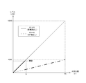
- FIG. 9 is a graph showing an example of the relationship between the amount of incident light and the level of a pixel signal according to the first embodiment of the present technology.
- the vertical axis in the figure is a value representing the level of the digital signal in the unit of LSB (Least Significant Bit).
- the horizontal axis in the figure is the amount of incident light on the pixel.
- the solid line indicates the characteristic of the digital signal Dout1 indicating the difference between the P1 level and the D1 level, and the dashed line indicates the characteristic of the digital signal Dout2 indicating the difference between the P2 level and the D2 level.
- the output range of the ADC 420 having a gradation of 12 bits is 4095 LSB
- the output value is saturated when the amount of incident light is N (e ⁇ ) in the case of differential reading, whereas it is 4N (e) in the case of SF reading. -) does not saturate up to.
- the dynamic range can be expanded to four times (in other words, +12 decibels) as compared with the read only of the differential read.
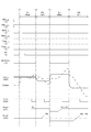
- FIG. 10 is a timing chart illustrating an example of differential reading in the first embodiment of the present technology.
- the vertical drive unit 12 supplies the drive signals RST (i, 2k) and RST (i, 2k + 1) at a timing T1, and supplies the drive signal TRG (i, 2k) at a timing T3. Then, the vertical drive unit 12 supplies the drive signals RST (i, 2k) and RST (i, 2k + 1) at timing T5, and supplies the drive signal TRG (i, 2k + 1) at timing T7.
- the drive signals SEL (i, 2k) and SEL (i, 2k + 1) are controlled to a high level.
- the system control unit 16 sets the drive signal SFEN to low level and sets the drive signal DAEN to high level.
- a differential amplifier circuit is configured.
- the system control unit 16 sets the drive signal DAS1 to a low level and the drive signal DAS2 to a high level from immediately before the timing T1 to immediately before the timing T5.
- the pixel (i, 2k) becomes a readout pixel
- the pixel (i, 2k + 1) becomes a reference pixel.
- the system control unit 16 sets the drive signal DAS1 to high level and sets the drive signal DAS2 to low level.
- the reference pixel and the readout pixel are exchanged.
- the P1 level pixel signal Vout 2k (differential amplified signal) is read during the period from timing T1 to T3, and the D1 level pixel signal Vout 2k is read during the period from timing T3 to T5.
- the P1 level pixel signal Vout 2k + 1 is read during the period from timing T5 to T7, and the D1 level pixel signal Vout 2k + 1 is read after timing T7.
- the above-described differential reading is performed within a 1 V period in the differential mode.
- SF reading is performed in addition to the differential reading.
- FIG. 11 is a timing chart illustrating an example of SF reading according to the first embodiment of the present technology.
- the vertical drive unit 12 supplies the drive signal RST (i, 2k) at the timing T2 and supplies the drive signal TRG (i, 2k) at the timing T4. Then, the vertical drive unit 12 supplies the drive signal RST (i, 2k + 1) at a timing T6, and supplies the drive signal TRG (i, 2k + 1) at a timing T8.
- the drive signal SEL (i, 2k) is controlled to a high level until immediately before timing T6, and SEL (i, 2k + 1) is controlled to a low level. After that, the drive signal SEL (i, 2k) is controlled to low level, and SEL (i, 2k + 1) is controlled to high level.
- the system control unit 16 sets the drive signal SFEN to high level and sets the drive signal DAEN to low level. This constitutes a source follower circuit.
- the drive signals DAS1 and DAS2 are controlled to a low level.
- the pixel signal Vout 2k of P2 level within the period of time T2 to T4 is read, D2 level of the pixel signal Vout 2k is read within a period of time T4 to T6.
- Pixel signal Vout 2k + 1 of the P2 level within the period of the timing T6 to T8 are read, the pixel signals Vout 2k + 1 of the D2 level after the timing T8 is read.
- FIG. 12 is a timing chart illustrating an example of control for reading out a pixel signal according to the first embodiment of the present technology. This readout control is executed each time the 1 V period elapses (in other words, each time the exposure of the reference pixel and the readout pixel ends).
- the vertical drive unit 12 supplies the drive signals RST (i, 2k) and RST (i, 2k + 1) at a timing T1, and supplies the drive signal TRG (i, 2k) at a timing T3.
- the drive signals SEL (i, 2k) and SEL (i, 2k + 1) are controlled to a high level.
- the system control unit 16 supplies the driving signal AZ at the timing T1, sets the AMPMODE indicating whether or not the differential reading is performed to the low level between the timings T1 and T2, and sets the AMPMODE to the low level between the timings T2 and T3.
- AMPMODE is set to a high level.
- the comparator 520 compares the pixel signal Vout 2k with the reference signal V slope and outputs a comparison result Vcm.
- the system control unit 16 sets an initial value (such as “0”) in the counter 421 and causes the counter 421 to start counting.
- the counter 421 counts until the comparison result Vcm is inverted. Thereby, the P1 level from the differential amplifier circuit is converted into a digital signal.
- the system control unit 16 sets an initial value (“0” or the like) in the counter 422 at the timing T2, and causes the counter 422 to start counting.
- the counter 422 counts until the comparison result Vcm is inverted. As a result, the P2 level from the source follower circuit is converted into a digital signal.
- the system control unit 16 Inverts the sign of the value held by the counter 421 and causes the counter 421 to start counting from the value.
- the counter 421 counts until the comparison result Vcm is inverted. Thereby, the D1 level from the differential amplifier circuit is converted into a digital signal. Since the counting is started from the inverted value of the P1 level, the digital signal Dout1 at the end of the counting indicates the difference between the D1 level and the P1 level.
- the system control unit 16 Inverts the sign of the value held by the counter 422, and causes the counter 422 to start counting from that value after timing T4.
- the counter 422 counts until the comparison result Vcm is inverted.
- the D2 level from the source follower circuit is converted into a digital signal. Since the counting is started from the inverted value of the D2 level, the digital signal Dout2 at the end of the counting indicates the difference between the D2 level and the P2 level.
- the column readout circuit unit 13 reads out in the order of the P1 level, the P2 level, the D1 level, and the D2 level, but is not limited to this order. Further, as described later, only one of the D1 level and the D2 level can be read. That is, the column readout circuit unit 13 reads out the P1 level and the P2 level and at least one of the D1 level and the D2 level.
- FIG. 13 is a diagram illustrating an example of an operation of the column readout circuit unit 13 and the column signal processing unit 14 according to the first embodiment of the present technology and a comparative example.
- “A” in the figure shows an example of the operation in the HDR mode of the first embodiment.
- “B” in the figure shows an example of the operation of the comparative example in which only one of the differential reading and the SF reading is performed within the 1 V period.
- the column readout circuit unit 13 in the HDR mode sequentially performs the differential readout and the SF readout at the end of the exposure during the 1 V period (eg, 1/60 second) from timing T0 to timing T10. Further, the column signal processing unit 14 combines the signal read differentially and the signal read SF, and generates an HDR frame. Similarly, after the timing T10, each time the 1 V period elapses (in other words, each time the exposure ends), the differential reading and the SF reading are sequentially performed. As a result, every time the 1 V period elapses, a synthesized frame having a wide dynamic range is generated.
- the 1 V period eg, 1/60 second
- the column readout circuit unit 13 performs only the differential readout at the end of the exposure during the 1 V period from the timing T0 to the timing T10. Then, in the next 1 V period from the timing T10 to the timing T20, the column readout circuit unit 13 performs only the SF readout at the end of the exposure.
- the column signal processing unit 14 can generate a synthesized frame by synthesizing a frame obtained by differential reading and a frame obtained by SF reading.
- the solid-state imaging device can also read out a plurality of frames by changing the exposure time only in the SF mode and combine them. In this case, similarly, a synthesized frame having a wide dynamic range can be generated.
- the dynamic range can be expanded, but the frame rate of the synthesized frame is reduced.
- the frame rate of the synthesized frame is reduced. For example, when a plurality of frames are imaged at a frame rate of 60 Hertz (Hz) and are synthesized two by two, the frame rate of the synthesized frame is reduced to 30 Hertz (Hz).
- FIG. 14 is a flowchart illustrating an example of an operation of the solid-state imaging device 10 according to the first embodiment of the present technology. This operation is started, for example, when the HDR mode is set.
- the vertical drive unit 12 and the system control unit 16 select a pixel to be read (step S901), and control the pixel to generate a P1 level by differential reading (step S902). Then, the vertical drive unit 12 and the like generate the P2 level by SF reading (step S903), and generate the D1 level by differential reading (step S904). The vertical drive unit 12 and the like generate the D2 level by reading the SF (step S905).
- the ADC 420 performs the CDS processing (Step S906), and the combining processing unit 430 determines whether or not the difference between the D2 level and the P2 level related to SF reading exceeds a threshold (that is, high illuminance) (Step S906). Step S907).
- step S907: Yes the synthesis processing unit 430 selects the digital signal Dout2 indicating the difference between the D2 level and the P2 level, and outputs the digital signal Dout2 as pixel data SIG (step S908).
- step S907: No the combining processing unit 430 selects the digital signal Dout1 indicating the difference between the D1 level and the P1 level, and outputs the digital signal Dout1 as pixel data SIG (step S909).
- step S910 determines whether or not reading of all pixels has been completed. If the reading of all pixels has not been completed (step S910: No), the vertical drive unit 12 repeats step S901 and subsequent steps. On the other hand, when the reading of all pixels is completed (step S910: Yes), the solid-state imaging device 10 ends the operation for imaging. When two or more synthesized frames are continuously imaged, the processing of steps S901 to S910 is repeatedly performed in synchronization with the vertical synchronization signal.
- the solid-state imaging device 10 combines the differentially amplified signal with the large gain and the pixel signal in the SF mode with the small gain, so that the solid-state imaging device 10 does not combine the signals. Can also widen the dynamic range.
- the solid-state imaging device 10 performs the differential reading. However, while the differential reading can increase the signal amplification factor, the noise may be amplified. .
- the solid-state imaging device 10 according to the second embodiment differs from the first embodiment in that noise is suppressed by connecting nodes in the column readout circuit unit 13 sideways.
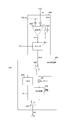
- FIG. 15 is a circuit diagram illustrating a configuration example of the unit readout circuit 300 according to the second embodiment of the present technology.
- the unit read circuit 300 according to the second embodiment is different from the first embodiment in that switches 315, 333, and 334 are further provided.
- the switch 315 connects the gates of the P-type transistors 311 and 312 and one end of each of the switches 313 and 314 to a horizontal signal line wired in the horizontal direction according to a drive signal DAHZ from the system control unit 16. For example, when the high-level drive signal DAHZ is supplied, the switch 315 is turned on.
- the system control unit 16 can connect a plurality of current mirror circuits arranged in the horizontal direction by horizontal connection.
- the switch 333 connects a connection point between the current source 331 and the switch 326 and a connection point between the current source 332 and the switch 328 according to a drive signal DAEN from the system control unit 16. For example, when the high-level drive signal DAEN is supplied, the switch 333 connects the current sources 331 and 332.
- the switch 334 connects a connection point between the current source 332 and the switch 328 and a connection point between the current source 331 and the switch 326 in the adjacent unit readout circuit 300 according to the drive signal DAHZ. For example, when the high-level drive signal DAHZ is supplied, the switch 334 connects the current sources 332 and 331.
- the system control unit 16 can connect a plurality of current sources arranged in a horizontal direction by supplying a high-level drive signal DAEN or DAHZ.
- switches 315, 333 and 334 are arranged, only the switch 315 or only the switches 333 and 334 can be arranged. By arranging them all, the effect of noise suppression can be improved.
- the present invention is not limited to the case where all pixel pairs (differential pairs) of the pixel array arranged in the pixel array unit 11 are connected, and the effect of noise reduction can be obtained by connecting the pixels horizontally in units of two or more columns.
- R Red
- G Green
- B Blue
- FIG. 16 is a timing chart showing an example of differential reading in the second embodiment of the present technology.
- the system control unit 16 further supplies a high-level drive signal DAHZ. Thereby, at the time of differential reading, noise can be suppressed by horizontal connection.
- FIG. 17 is a timing chart showing an example of SF reading according to the second embodiment of the present technology.
- the system control unit 16 further supplies a low-level drive signal DAHZ.
- the switches 315, 333, and 334 horizontally connect the current mirror circuit and the current source during differential reading, so that noise is suppressed and signal quality is reduced. Can be improved.
- the counters 421 and 422 are arranged and counted for every two columns. However, as the number of columns increases, the circuit scale may increase.
- the solid-state imaging device 10 according to the third embodiment is different from the first embodiment in that one counter is reduced for every two columns.
- FIG. 18 is a circuit diagram illustrating a configuration example of the ADC 420 and the synthesis processing unit 430 according to the third embodiment of the present technology.
- the ADC 420 according to the third embodiment is different from the first embodiment in that the counter 422 is not provided.
- the combination processing unit 430 according to the third embodiment is different from the first embodiment in further including a switch 434 and a memory 435.
- the ADC 420 according to the third embodiment outputs a digital signal Dout.
- the switch 434 supplies the digital signal Dout to one of the multiplier 431 and the memory 435 under the control of the system control unit 16.
- the switch 434 selects one of the digital signal Dout2 which is a digital signal Dout at the time of SF reading and the digital signal Dout1 held in the memory 435.
- FIG. 19 is a timing chart showing an example of the operation of the solid-state imaging device 10 according to the third embodiment of the present technology.
- the vertical driver 12 generates the P1 level by differential reading between the timings T1 and T2, and generates the D1 level by differential reading between the timings T2 and T3.
- the system control unit 16 Inverts the sign of the count value of the counter 421.
- the digital signal Dout at the end of the counting indicates a difference between the D1 level and the P1 level.
- the system control unit 16 controls the switch 434 to cause the memory 435 to hold the difference between the D1 level and the P1 level as a digital signal Dout1.
- the vertical drive unit 12 generates the D2 level by the SF reading, and generates the P2 level by the differential reading after the timing T4. Further, the system control unit 16 initializes the counter 421 at the timing T3, and inverts the sign of the count value at the timing T4. Thus, the digital signal Dout at the end of the counting indicates a difference between the D2 level and the P2 level.
- the system control unit 16 controls the switch 434 to supply the difference between the D2 level and the P2 level to the multiplier 431 as a digital signal Dout2.
- the difference between the D2 level and the P2 level is a DDS (Double Data Sampling) read signal having no correlation of the kTC noise in the floating diffusion region.
- DDS Double Data Sampling
- noise increases compared to the CDS read.
- SF reading is for a bright signal, and the light shot noise is dominant in the bright state, so that the influence of the noise increase can be ignored.
- the combining processing unit 430 selects either the digital signal Dout1 for differential reading or the digital signal Dout2 for SF reading, which is held in the memory 435. Thus, the HDR combining process is performed.
- the counter 421 calculates the difference between the P1 level and the D1 level, and the D2 level and the P2 level. And the level difference can be obtained in order.
- the counter 422 that operates in parallel with the counter 421 and obtains the difference between the P2 level and the D2 level can be reduced.
- the ADC 420 performs AD conversion on all of the P1, D1, D2, and P2 levels. However, as the number of columns increases, the number of conversions increases and power consumption increases. There is a possibility that.
- the ADC 420 according to the modification of the third embodiment is different from the third embodiment in that the AD conversion of the D2 level and the P2 level related to SF reading is stopped at low illuminance to reduce power consumption.
- FIG. 20 is a timing chart illustrating an example of an operation of the solid-state imaging device 10 according to a modification of the third embodiment of the present technology.
- the system control unit 16 according to the modification of the third embodiment refers to the determination result of the determination circuit 432 at the timing T3, and the difference between the D1 level and the P1 level exceeds the threshold (that is, the illuminance is higher than a predetermined value). ) Is determined. When the illuminance is equal to or less than the predetermined value, the system control unit 16 disables the counter 421 and stops the AD conversion of the D2 level and the P2 level.
- the system control unit 16 operates the counter 421 to AD-convert the D2 level and the P2 level.
- the counter 421 when the illuminance is equal to or less than the predetermined value, the counter 421 does not perform the AD conversion of the D2 level and the P2 level. Power consumption can be reduced as compared with the case of performing the conversion.
- the ADC 420 reads out all of the P1, P2, D1, and D2 levels and performs AD conversion. However, as the number of columns increases, the number of conversions increases, and the reading speed increases. May decrease.
- the ADC 420 according to the modification of the fourth embodiment differs from the third embodiment in that the reading speed is improved by reading only one of the D1 level and the D2 level.
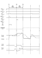
- FIG. 21 is a timing chart showing an example of the operation of the solid-state imaging device at low illuminance in the fourth embodiment of the present technology.
- the vertical driver 12 generates the P1 level by differential reading between the timings T1 and T2, and generates the P2 level by SF reading from the timing T2 to T3.
- the system control unit 16 controls the switch 434 to cause the memory 435 to hold the P1 level. Then, at a predetermined timing immediately after the timing T3, the system control unit 16 refers to the comparison result Vcm of the comparator 520 and determines whether or not the comparison result Vcm is inverted (that is, the illuminance is higher than a predetermined value). When the illuminance is equal to or less than the predetermined value, the system control unit 16 initializes the count value of the counter 421 to -P1. Also, the vertical drive unit 12 refers to the comparison result Vcm, and generates the D1 level by differential reading when the illuminance is equal to or less than a predetermined value. The count value of the counter 421 at the end of counting is the difference between the D1 level and the P1 level. The difference between the D1 level and the P1 level is output as it is as pixel data SIG.
- the column signal processing unit 14 of the fourth embodiment is different from the third embodiment in that only the memory 435 is arranged instead of the synthesis processing unit 430.
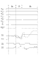
- FIG. 22 is a timing chart showing an example of the operation of the solid-state imaging device at high illuminance according to the fourth embodiment of the present technology.
- the control up to the timing T3 is the same as at the time of low illuminance.
- the system control unit 16 refers to the comparison result Vcm and determines whether the illuminance is higher than a predetermined value. When the illuminance is higher than the predetermined value, the system control unit 16 inverts the sign of the count value P2 of the counter 421.
- the vertical drive unit 12 also refers to the comparison result Vcm, and generates a D2 level by differential reading when the illuminance is higher than a predetermined value.
- the count value at the end of counting by the counter 421 is a difference between the D2 level and the P2 level.
- the difference between the D2 level and the P2 level is output as it is as pixel data SIG.
- the read speed is reduced as compared with the case where both of them are AD-converted. Can be improved. As a result, the frame rate of the synthesized frame can be improved.
- the differential readout is performed with the pixels 220 and 230 adjacent in the horizontal direction as the readout pixel and the reference pixel.
- the number of horizontal signal lines between the vertical driving unit 12 and the pixel array unit 11 may increase.
- the solid-state imaging device 10 according to the fifth embodiment differs from the first embodiment in that the number of horizontal signal lines is reduced by using pixels 220 and 230 adjacent in the vertical direction as readout pixels and reference pixels.
- FIG. 23 is a plan view illustrating an example of the pixel array unit 11 according to the fifth embodiment of the present technology.
- the pixel array section 11 of the fifth embodiment is different from the pixel array section 11 of the first embodiment in that the pixels 220 are arranged in 2k rows, which are even rows, and the pixels 230 are arranged in 2k + 1 rows, which are odd rows. And different.
- vertical signal lines VSL 2k and VSL 2k + 1 , vertical reset input lines VRD 2k and VRD 2k + 1 , and vertical current supply lines VCOM 2k and VCOM 2k + 1 are wired for each column.
- the pixel 220 is connected to a vertical signal line VSL 2k , a vertical reset input line VRD 2k, and a vertical current supply line VCOM 2k .
- the pixel 230 is connected to a vertical signal line VSL 2k + 1 , a vertical reset input line VRD 2k + 1, and a vertical current supply line VCOM 2k + 1 .
- the pixel 220 and the pixel 230 forming a pair may be arranged at positions where both the vertical address and the horizontal address are different from each other.
- the pixel 220 is arranged at the address (i, j)
- the pixel 230 is arranged at the lower right address (i + 1, j + 1).
- the vertical driving unit 12 since the vertical driving unit 12 drives the pixels 220 and 230 that are adjacent in the vertical direction, the horizontal signal line transmitting the driving signal from the vertical driving unit 12 is used. Can be reduced.
- the differential readout is performed by replacing the readout pixel and the reference pixel.
- the solid-state imaging device 10 according to the sixth embodiment differs from the first embodiment in that the positions of the reference pixels are fixed and the number of switches is reduced.
- FIG. 25 is a plan view illustrating an example of the pixel array unit 11 according to the sixth embodiment of the present technology.
- a plurality of readout pixels 240 and a plurality of reference pixels 250 are arranged in a two-dimensional lattice.
- the reference pixels 250 are arranged in a specific row, for example.
- the readout pixels 240 are arranged in a different row from the reference pixels 250.
- the readout pixel 240 includes a photodiode 241, a transfer transistor 242, a floating diffusion region 246, a reset transistor 243, an amplification transistor 244, and a selection transistor 245.
- the connection configuration of these elements is similar to that of the pixel 220.
- the reference pixel 250 is a pseudo pixel that exhibits the same reset feedthrough characteristic as the read pixel 240.
- the reference pixel 250 includes a photodiode 251, a transfer transistor 252, a floating diffusion region 256, a reset transistor 253, an amplification transistor 254, and a selection transistor 255.
- the connection configuration of these elements is similar to that of the pixel 220.
- a pixel having the same configuration as the read pixel 240 except that the number of light-shielded pixels and photodiodes is reduced can be disposed as the reference pixel 250.
- the unit readout circuit 300 is arranged for each column, and reads out a differentially amplified signal from the reference pixel 250 and one of the readout pixels 240 in the corresponding column.
- the unit readout circuit 300 is not provided with a switch (switch 313 and the like) group for replacing the readout pixel and the reference pixel.
- the circuit scale can be reduced.
- the ordinary current mirror circuit in which the P-type transistors 311 and 312 are connected in parallel to the power supply voltage is used.
- the output from the current mirror circuit is caused by the fluctuation of the power supply voltage.
- the pixel signal Vout may fluctuate.
- the solid-state imaging device 10 according to the seventh embodiment differs from the first embodiment in that a cascode current mirror circuit suppresses the influence of fluctuations in power supply voltage.
- FIG. 26 is a circuit diagram illustrating a configuration example of a differential amplifier circuit according to the seventh embodiment of the present technology.
- the differential amplifier circuit according to the seventh embodiment is different from the first embodiment in that the unit read circuit 300 further includes P-type transistors 345 and 346.
- P-type transistor 345 is cascode-connected to P-type transistor 311, and P-type transistor 346 is cascode-connected to P-type transistor 312.
- the drain and the gate of the P-type transistor 345 are connected to, for example, the reference-side vertical signal line VSL 2k .
- the drain of the P-type transistor 346 is connected to, for example, the vertical signal line VSL 2k + 1 on the read side.
- Such a current mirror circuit is called a cascode current mirror circuit.
- the pixel signal Vout due to the fluctuation of the power supply voltage is compared with the case where the normal current mirror circuit that is not cascode-connected is disposed. Can be suppressed.
- the switch 410, the ADC 420, and the synthesis processing unit 430 are arranged for each column in the column signal processing unit 14. However, as the number of columns increases, the circuit scale of the column signal processing unit 14 increases. May increase.
- the solid-state imaging device 10 according to the eighth embodiment differs from the first embodiment in that the number of switches 410 is reduced.
- FIG. 27 is a circuit diagram illustrating a configuration example of a differential amplifier circuit according to the eighth embodiment of the present technology.
- the differential amplifier circuit according to the eighth embodiment differs from the first embodiment in that switches 351 and 352 are further arranged in the unit readout circuit 300.
- the switch 351 connects the vertical signal line VSL 2k to the column signal processing unit 14 according to the drive signal SW1 from the system control unit 16. For example, when the high-level drive signal SW1 is supplied, the switch 351 connects the vertical signal line VSL 2k to the column signal processing unit 14.
- the switch 352 connects the vertical signal line VSL 2k + 1 to the column signal processing unit 14 according to the drive signal SW2 from the system control unit 16. For example, when the high-level drive signal SW2 is supplied, the switch 352 connects the vertical signal line VSL 2k + 1 to the column signal processing unit 14.
- the drive signal SW3 is input to the switch 313, and the drive signal SW4 is input to the switch 314.
- the drive signal SW5 is input to the switch 317, and the drive signal SW6 is input to the switch 318.
- the drive signal SW7 is input to the switch 322, and the drive signal SW8 is input to the switch 323.
- the switch 410 is not provided in the column signal processing unit 14 according to the eighth embodiment.
- FIG. 28 is a timing chart illustrating an example of an operation of the solid-state imaging device 10 according to the eighth embodiment of the present technology.
- the vertical drive unit 12 supplies the drive signals RST (i, 2k) and TRG (i, 2k) to start exposure of the pixel (i, 2k).
- the vertical drive unit 12 supplies the drive signals RST (i, 2k + 1) and TRG (i, 2k + 1) to start exposure of the pixel (i, 2k + 1).
- the vertical drive unit 12 supplies the drive signals RST (i, 2k) and RST (i, 2k + 1) to generate a P-phase level.
- the vertical drive unit 12 supplies the drive signal TRG (i, 2k) , ends the exposure of the pixel (i, 2k), and generates a D-phase level.
- the vertical drive unit 12 supplies the drive signals RST (i, 2k) and RST (i, 2k + 1) to generate a P-phase level.
- the vertical drive unit 12 supplies the drive signal TRG (i, 2k + 1) , ends the exposure of the pixel (i, 2k + 1), and generates a D-phase level.
- the system control unit 16 supplies the drive signal SW8 at the timing T10, and supplies the drive signal SW5 at the timing T11.
- the system control unit 16 sets the drive signals SW2, SW3, SW5, and SW8 to high level and the rest to low level during the timing T12 to T14.
- the system control unit 16 sets the drive signals SW1, SW4, SW6, and SW7 to high level and sets the rest to low level during the timings T14 to T16.
- the P1 level is AD-converted between the timings T12 and T13
- the D1 level is AD-converted between the timings T13 and T14
- the P2 level is AD-converted between timings T14 and T15
- the D2 level is AD-converted between timings T15 and T16.
- the switches 351 and 352 for switching the vertical signal lines are arranged in the unit readout circuit 300, the switches having the same functions as those in the column signal processing unit 14 are provided. There is no need to arrange the 410. Thereby, the circuit scale of the column signal processing unit 14 can be reduced.
- the AD conversion is performed using the reference signal V slope having the same amplitude range as that in the SF reading.
- the power consumption is sufficiently reduced. May not be possible.
- the solid-state imaging device 10 according to the ninth embodiment differs from the first embodiment in that the current in the DAC is controlled to reduce power consumption.
- FIG. 29 is a block diagram illustrating a configuration example of a solid-state imaging device 10 according to a ninth embodiment of the present technology.
- a DAC 510 is arranged in the solid-state imaging device 10 according to the ninth embodiment.
- the DAC 510 generates a reference signal V slope according to a control signal from the system control unit 16 and supplies the reference signal V slope to the comparator 520.
- FIG. 30 is a circuit diagram illustrating a configuration example of a DAC 510 and a comparator 520 according to the ninth embodiment of the present technology.
- the DAC 510 includes a P-type transistor 511, a current source 512, a plurality of P-type transistors 513, a plurality of switches 514, and a variable resistor 515.
- M is an integer
- P-type transistors 513 are arranged, and a switch 514 is provided for each P-type transistor 513.
- MOS transistors are used as these P-type transistors.
- the current source 512 is for generating a predetermined reference current.
- the system control unit 16 can control the value of the reference current. For example, the system control unit 16 generates a reference current I DA_D in differential reading, and generates a reference current I DA_S different from I DS_A in SF reading.
- the P-type transistor 511 and the plurality of P-type transistors 513 are connected in parallel to a power supply voltage terminal. Further, the gate of the P-type transistor 511 is connected to each gate of the plurality of P-type transistors 513. The drain of the P-type transistor 511 is connected to the current source 512 and its own gate.
- the switch 514 connects the drain of the corresponding P-type transistor 513 to the variable resistor 515 according to the control signal SW2m (m is an integer of 1 to M) from the system control unit 16. For example, when the high-level control signal SW2m is supplied, the switch 514 connects the drain of the corresponding P-type transistor 513 to the variable resistor 515.
- a reference signal V slope is output from a connection point between the variable resistor 515 and the switch 514.
- the system controller 16 can control the resistance value of the variable resistor 515. For example, the resistance value is controlled to R_D in differential reading, and the resistance value is R_S in SF reading.
- the above-described P-type transistor 511 and the M P-type transistors 513 form a current mirror circuit.
- the system control unit 16 turns on and off the M switches 514 in a time sharing manner, fluctuates the current flowing from the current mirror circuit to the variable resistor 515, and generates a slope-shaped reference signal V slope .
- Comparator 520 includes P-type transistors 521, 522 and 523, N-type transistors 524 and 525, and current sources 526 and 527. As these transistors, for example, MOS transistors are used.
- P-type transistors 521 and 522 are connected in parallel to a power supply voltage terminal.
- the gate of the P-type transistor 521 is connected to its own drain and the gate of the P-type transistor 522.
- the drain of the P-type transistor 521 is connected to the drain of the N-type transistor 524.
- the drain of P-type transistor 522 is connected to the gate of P-type transistor 523 and the drain of N-type transistor 525.
- N-type transistors 524 and 525 form a differential pair, and a reference signal V slope is input to the gate of N-type transistor 524.
- an analog signal Ain is input to a gate of the N-type transistor 525.
- Sources of N-type transistors 524 and 525 are commonly connected to current source 526.
- the P-type transistor 523 and the current source 527 are connected in series to the power supply voltage terminal, and the comparison result Vcm is output from the connection point.
- the tail current flowing to the current source 526 at the time of differential reading is defined as ICM_D1
- the output current flowing to the current source 527 is defined as ICM_D2 .
- the tail current flowing to the current source 526 at the time of SF reading is defined as ICM_S1
- the output current flowing to the current source 527 is defined as ICM_S2 .
- a load MOS circuit 530 is connected to a signal line for transmitting the analog signal Ain.
- the load current flowing through the load MOS circuit 530 at the time of differential reading is ILM_D
- the load current flowing at the time of SF reading is ILM_S .
- there are disadvantages such as an increase in power consumption and a decrease in the amplitude range of the output signal.
- the load currents I LM_D and I LM_S have different current values, and a current value suitable for each read mode can be set by controlling the reference current.
- the reference currents I DA_D and I DA_S have different current values, and a current value suitable for each read mode can be set by the control of the system control unit 16. For example, assume that the reference current I DA_D is smaller than the reference current I DA_S and the resistance value R_D is larger than the resistance value R_S. In the DAC 510, the thermal noise of the variable resistor 515 is a dominant component of the total noise, and the lower the resistance value, the lower the noise.
- the current values of the tail current ICM_D1 and the tail current ICM_S1 are different, and the current values of the output current ICM_D2 and the output current ICM_S2 are different.
- the tail current I CM_D1 smaller than the tail current I CM_S1, when less than the output current I CM_S2 the output current I CM_D2, it is possible to reduce the power consumption in the differential read. Instead, the noise of the comparator 520 deteriorates, but the conversion efficiency is increased by the differential reading, so that the image quality effect of the subsequent noise deterioration is negligible.
- the reference current and the load current in the DAC 510 are reduced during the differential reading, so that the power consumption during the differential reading can be reduced.
- the technology (the present technology) according to the present disclosure can be applied to various products.
- the technology according to the present disclosure is realized as a device mounted on any type of moving object such as an automobile, an electric vehicle, a hybrid electric vehicle, a motorcycle, a bicycle, a personal mobility, an airplane, a drone, a ship, and a robot. May be.
- FIG. 31 is a block diagram illustrating a schematic configuration example of a vehicle control system that is an example of a moving object control system to which the technology according to the present disclosure can be applied.
- Vehicle control system 12000 includes a plurality of electronic control units connected via communication network 12001.
- the vehicle control system 12000 includes a drive system control unit 12010, a body system control unit 12020, an outside information detection unit 12030, an inside information detection unit 12040, and an integrated control unit 12050.
- a microcomputer 12051, an audio / video output unit 12052, and a vehicle-mounted network I / F (interface) 12053 are illustrated.
- the drive system control unit 12010 controls the operation of the device related to the drive system of the vehicle according to various programs.
- the drive system control unit 12010 includes a drive force generation device for generating a drive force of the vehicle such as an internal combustion engine or a drive motor, a drive force transmission mechanism for transmitting the drive force to wheels, and a steering angle of the vehicle. It functions as a control device such as a steering mechanism for adjusting and a braking device for generating a braking force of the vehicle.
- the body control unit 12020 controls the operation of various devices mounted on the vehicle body according to various programs.
- the body control unit 12020 functions as a keyless entry system, a smart key system, a power window device, or a control device for various lamps such as a head lamp, a back lamp, a brake lamp, a blinker, a fog lamp, and the like.
- a radio wave or various switch signals transmitted from a portable device that substitutes for a key may be input to the body control unit 12020.
- the body control unit 12020 receives the input of these radio waves or signals, and controls a door lock device, a power window device, a lamp, and the like of the vehicle.
- Out-of-vehicle information detection unit 12030 detects information outside the vehicle on which vehicle control system 12000 is mounted.
- an imaging unit 12031 is connected to the outside-of-vehicle information detection unit 12030.
- the out-of-vehicle information detection unit 12030 causes the imaging unit 12031 to capture an image of the outside of the vehicle, and receives the captured image.
- the outside-of-vehicle information detection unit 12030 may perform an object detection process or a distance detection process of a person, a vehicle, an obstacle, a sign, or a character on a road surface based on the received image.
- the imaging unit 12031 is an optical sensor that receives light and outputs an electric signal according to the amount of received light.
- the imaging unit 12031 can output the electric signal as an image or can output the electric signal as distance measurement information.
- the light received by the imaging unit 12031 may be visible light or non-visible light such as infrared light.
- the in-vehicle information detection unit 12040 detects information in the vehicle.
- the in-vehicle information detection unit 12040 is connected to, for example, a driver status detection unit 12041 that detects the status of the driver.
- the driver state detection unit 12041 includes, for example, a camera that captures an image of the driver, and the in-vehicle information detection unit 12040 determines the degree of fatigue or concentration of the driver based on the detection information input from the driver state detection unit 12041. The calculation may be performed, or it may be determined whether the driver has fallen asleep.
- the microcomputer 12051 calculates a control target value of the driving force generation device, the steering mechanism, or the braking device based on the information on the inside and outside of the vehicle acquired by the outside information detection unit 12030 or the inside information detection unit 12040, and the drive system control unit.
- a control command can be output to 12010.
- the microcomputer 12051 implements functions of ADAS (Advanced Driver Assistance System) including a vehicle collision avoidance or shock mitigation, a following operation based on an inter-vehicle distance, a vehicle speed maintenance operation, a vehicle collision warning, or a vehicle lane departure warning.
- ADAS Advanced Driver Assistance System
- the cooperative control for the purpose can be performed.
- the microcomputer 12051 controls the driving force generation device, the steering mechanism, the braking device, and the like based on information on the surroundings of the vehicle acquired by the outside-of-vehicle information detection unit 12030 or the inside-of-vehicle information detection unit 12040, so that the driver's It is possible to perform cooperative control for automatic driving or the like in which the vehicle travels autonomously without relying on the operation.
- the microcomputer 12051 can output a control command to the body system control unit 12020 based on information on the outside of the vehicle acquired by the outside information detection unit 12030.
- the microcomputer 12051 controls the headlamp according to the position of the preceding vehicle or the oncoming vehicle detected by the outside-of-vehicle information detection unit 12030, and performs cooperative control for the purpose of preventing glare such as switching a high beam to a low beam. It can be carried out.
- the audio image output unit 12052 transmits at least one of an audio signal and an image signal to an output device capable of visually or audibly notifying a passenger of the vehicle or the outside of the vehicle of information.
- an audio speaker 12061, a display unit 12062, and an instrument panel 12063 are illustrated as output devices.
- the display unit 12062 may include, for example, at least one of an on-board display and a head-up display.
- FIG. 32 is a diagram illustrating an example of an installation position of the imaging unit 12031.
- imaging unit 12031 there are imaging units 12101, 12102, 12103, 12104, and 12105.
- the imaging units 12101, 12102, 12103, 12104, and 12105 are provided, for example, at positions such as a front nose, a side mirror, a rear bumper, a back door, and an upper portion of a windshield in the vehicle interior of the vehicle 12100.
- An imaging unit 12101 provided in the front nose and an imaging unit 12105 provided above a windshield in the vehicle cabin mainly acquire an image in front of the vehicle 12100.
- the imaging units 12102 and 12103 provided in the side mirror mainly acquire images of the side of the vehicle 12100.
- the imaging unit 12104 provided in the rear bumper or the back door mainly acquires an image behind the vehicle 12100.
- the imaging unit 12105 provided above the windshield in the passenger compartment is mainly used for detecting a preceding vehicle or a pedestrian, an obstacle, a traffic light, a traffic sign, a lane, or the like.
- FIG. 32 shows an example of the imaging range of the imaging units 12101 to 12104.
- the imaging range 12111 indicates the imaging range of the imaging unit 12101 provided on the front nose
- the imaging ranges 12112 and 12113 indicate the imaging ranges of the imaging units 12102 and 12103 provided on the side mirrors, respectively
- the imaging range 12114 indicates 14 shows an imaging range of an imaging unit 12104 provided in a rear bumper or a back door. For example, by overlaying image data captured by the imaging units 12101 to 12104, a bird's-eye view image of the vehicle 12100 viewed from above can be obtained.
- At least one of the imaging units 12101 to 12104 may have a function of acquiring distance information.
- at least one of the imaging units 12101 to 12104 may be a stereo camera including a plurality of imaging elements or an imaging element having pixels for detecting a phase difference.
- the microcomputer 12051 calculates the distance to each three-dimensional object in the imaging ranges 12111 to 12114 and the temporal change of this distance (relative speed with respect to the vehicle 12100). , It is possible to extract, as a preceding vehicle, a three-dimensional object that travels at a predetermined speed (for example, 0 km / h or more) in a direction substantially the same as the vehicle 12100, which is the closest three-dimensional object on the traveling path of the vehicle 12100. it can.
- a predetermined speed for example, 0 km / h or more
- microcomputer 12051 can set an inter-vehicle distance to be secured before the preceding vehicle, and perform automatic brake control (including follow-up stop control), automatic acceleration control (including follow-up start control), and the like. As described above, it is possible to perform cooperative control for automatic driving or the like in which the vehicle travels autonomously without depending on the operation of the driver.
- the microcomputer 12051 converts the three-dimensional object data relating to the three-dimensional object into other three-dimensional objects such as a two-wheeled vehicle, a normal vehicle, a large vehicle, a pedestrian, and a utility pole based on the distance information obtained from the imaging units 12101 to 12104. It can be classified and extracted and used for automatic avoidance of obstacles. For example, the microcomputer 12051 distinguishes obstacles around the vehicle 12100 into obstacles that are visible to the driver of the vehicle 12100 and obstacles that are difficult to see.
- the microcomputer 12051 determines a collision risk indicating a risk of collision with each obstacle, and when the collision risk is equal to or higher than the set value and there is a possibility of collision, the microcomputer 12051 transmits the signal via the audio speaker 12061 or the display unit 12062.
- driving assistance for collision avoidance can be performed.
- At least one of the imaging units 12101 to 12104 may be an infrared camera that detects infrared light.
- the microcomputer 12051 can recognize a pedestrian by determining whether or not a pedestrian exists in the captured images of the imaging units 12101 to 12104. The recognition of such a pedestrian is performed by, for example, extracting a feature point in an image captured by the imaging units 12101 to 12104 as an infrared camera, and performing a pattern matching process on a series of feature points indicating an outline of the object to determine whether the object is a pedestrian.
- the audio image output unit 12052 outputs a rectangular contour for emphasis to the recognized pedestrian.
- the display unit 12062 is controlled so that is superimposed. Further, the sound image output unit 12052 may control the display unit 12062 so as to display an icon or the like indicating a pedestrian at a desired position.
- the technology according to the present disclosure can be applied to the imaging unit 12031 in the configuration described above.
- the solid-state imaging device 10 in FIG. 1 can be applied to the imaging unit 12031.
- the processing procedure described in the above embodiment may be considered as a method having a series of these procedures, and a program for causing a computer to execute the series of procedures or a recording medium for storing the program. May be caught.
- a recording medium for example, a CD (Compact Disc), an MD (MiniDisc), a DVD (Digital Versatile Disc), a memory card, a Blu-ray Disc (Blu-ray (registered trademark) Disc), or the like can be used.
- the pair of pixels performs a process of outputting a differentially amplified signal obtained by amplifying a difference between generated voltages of the pair of pixels and a process of outputting a pixel signal of the generated voltage of at least one of the pair of pixels.
- a readout circuit for each exposure A solid-state imaging device comprising: a processing unit that performs a synthesis process of synthesizing the output differential amplified signal and the output pixel signal.
- the read circuit sets at least one of a first reset level obtained by differentially amplifying the reset level of each of the pair of pixels and a second reset level that is the reset level of one of the pair of pixels.
- the method according to (2) further comprising outputting a first signal level obtained by differentially amplifying the signal level of each of the pair of pixels and a second signal level which is the signal level of one of the pair of pixels.
- Solid-state imaging device (4) The solid-state imaging device according to (3), wherein the readout circuit outputs the first signal level and the second signal level after outputting the first reset level and the second reset level.
- the solid-state imaging device wherein the readout circuit further outputs the second signal level and the second reset level after outputting the first reset level and the first signal level.
- the processing unit converts the first reset level, the first signal level, the second signal level, and the second reset level into a digital signal in order, and An analog-to-digital converter that sequentially converts the first reset level and the first signal level into a digital signal when is less than the predetermined value;
- the solid-state imaging device according to (5) further including: a synthesis processing unit configured to perform the synthesis processing based on the digital signal.
- the processing unit selects and outputs the differential amplified signal when the illuminance is less than a predetermined value, and selects and outputs the pixel signal when the illuminance exceeds the predetermined value.
- the solid-state imaging device according to any one of (3) to (6).
- the readout circuit outputs one of the first signal level and the second signal level after outputting the first reset level and the second reset level.
- a plurality of unit read circuits each including a current mirror circuit, a current source, and a switch are arranged in a predetermined direction
- the solid-state imaging device according to any one of (1) to (8), wherein the switch connects the current mirror circuit and the current source of each of the plurality of unit readout circuits to each other.
- (10) further comprising a pixel array section in which a plurality of pixels are arranged in a two-dimensional lattice;
- the solid-state imaging device according to any one of (1) to (9), wherein the pair of pixels are arranged in the pixel array unit in a horizontal direction.
- the solid-state imaging device according to any one of (1) to (9), wherein the pair of pixels are vertically arranged in the pixel array unit.
- the image display apparatus further includes a pixel array unit in which a plurality of pixels to which a vertical address and a horizontal address are respectively assigned are arranged in a two-dimensional lattice.
- the solid-state imaging device according to any one of (1) to (9), wherein the pair of pixels are pixels in which both the vertical address and the horizontal address are different from each other in the pixel array unit.
- a pixel array unit in which a plurality of readout pixels and reference pixels associated with the plurality of readout pixels are arranged, One of the pair of pixels is any of the plurality of readout pixels, and the other of the pair of pixels is the reference pixel,
- the readout circuit performs a process of outputting a differential amplified signal obtained by amplifying a difference between a pixel signal of each of the readout pixel and the reference pixel and a process of outputting the pixel signal of the readout pixel.
- the solid-state imaging device according to any of (12).
- the solid-state imaging device wherein the current mirror circuit is a cascode current mirror circuit.
- the current mirror circuit is connected to a pair of vertical signal lines, The solid-state imaging device according to (14) or (15), wherein the readout circuit further includes a switch that selects one of the pair of vertical signal lines and connects to the processing unit.
- a digital-to-analog converter including a current source for generating a predetermined reference current and a resistor for generating a predetermined reference signal corresponding to the reference current; A system control unit that controls a value of the reference current,
- the solid-state imaging device according to any one of (1) to (16), wherein the processing unit includes a comparator that compares a signal output from the readout circuit with a predetermined reference signal.
- a pair of pixels The process of outputting a differential amplified signal obtained by amplifying the difference between the generated voltages of the pair of pixels and the process of outputting the pixel signal of the generated voltage of at least one of the pair of pixels are performed by exposing the pair of pixels.
- An imaging apparatus comprising: a processing unit that performs a combining process of combining the output differential amplified signal and the output pixel signal.
- the pair of pixels performs a process of outputting a differentially amplified signal obtained by amplifying a difference between generated voltages of the pair of pixels and a process of outputting a pixel signal of the generated voltage of at least one of the pair of pixels.
Landscapes
- Engineering & Computer Science (AREA)
- Multimedia (AREA)
- Signal Processing (AREA)
- Transforming Light Signals Into Electric Signals (AREA)
- Solid State Image Pick-Up Elements (AREA)
Abstract
差動増幅回路を設けた固体撮像素子において、フレームレートを低下させずにダイナミックレンジを広くする。 固体撮像素子は、読出し回路および処理部を具備する。読出し回路は、一対の画素のそれぞれの生成電圧の差分を増幅した差動増幅信号を出力する処理と一対の画素の少なくとも一方の前記生成電圧の画素信号を出力する処理とを前記一対の画素が露光されるたびに行う。処理部は、出力された差動増幅信号と出力された画素信号とを合成する合成処理を行う。
Description
本技術は、固体撮像素子、撮像装置、および、固体撮像素子の制御方法に関する。詳しくは、画素信号を差動増幅する固体撮像素子、撮像装置、および、固体撮像素子の制御方法に関する。
従来より、撮像装置などにおいて画像データを撮像するために固体撮像素子が用いられている。この固体撮像素子の個々の画素の感度が比較的低いと、環境光の光量が比較的少ない場合に、画像データが全体的に暗くなり、画質が低下するおそれがある。そこで、感度を高くするために、例えば、一対の画素にカレントミラー回路を接続し、それらの画素とカレントミラー回路とからなる差動増幅回路を構成する固体撮像素子が提案されている(例えば、特許文献1参照。)。
上述の従来技術では、差動増幅回路が、一対の画素のそれぞれの信号を差動増幅するため、カレントミラー回路を接続しない場合よりも画素の感度を高くすることができる。しかしながら、上述の固体撮像素子では、強い光により影が生じている場合など、環境光の光量の変動が激しい場合に、ダイナミックレンジが不足して画質が低下するおそれがある。露光時間の異なる複数枚の画像データ(フレーム)を撮像し、それらを合成すればダイナミックレンジの広い合成フレームが得られるが、その代わりにフレームレートが低下してしまう。例えば、60ヘルツ(Hz)のフレームレートで複数枚のフレームを撮像し、2枚ずつ合成する場合、合成フレームのフレームレートは30ヘルツ(Hz)に低下してしまう。このように、上述の固体撮像素子では、フレームレートを低下させずに画像データのダイナミックレンジを広くすることができないという問題がある。
本技術はこのような状況に鑑みて生み出されたものであり、差動増幅回路を設けた固体撮像素子において、フレームレートを低下させずにダイナミックレンジを広くすることを目的とする。
本技術は、上述の問題点を解消するためになされたものであり、その第1の側面は、一対の画素のそれぞれの生成電圧の差分を増幅した差動増幅信号を出力する処理と上記一対の画素の少なくとも一方の上記生成電圧の画素信号を出力する処理とを上記一対の画素が露光されるたびに行う読出し回路と、上記出力された差動増幅信号と上記出力された画素信号とを合成する合成処理を行う処理部とを具備する固体撮像素子、および、その制御方法である。これにより、差動増幅信号および画像信号の合成によってダイナミックレンジが拡大されるという作用をもたらす。
また、この第1の側面において、上記一対の画素のそれぞれは、初期化されたときに上記生成電圧としてリセットレベルを生成し、露光が終了したときに上記生成電圧として信号レベルを生成してもよい。これにより、リセットレベルおよび信号レベルから得られた信号の合成によってダイナミックレンジが拡大されるという作用をもたらす。
また、この第1の側面において、上記読出し回路は、上記一対の画素のそれぞれの上記リセットレベルを差動増幅した第1リセットレベルと上記一対の画素のいずれかの上記リセットレベルである第2リセットレベルとの少なくとも一方を出力するとともに上記一対の画素のそれぞれの上記信号レベルを差動増幅した第1信号レベルと上記一対の画素のいずれかの上記信号レベルである第2信号レベルとを出力してもよい。これにより、第1リセットレベルおよび第2リセットレベルの少なくとも一方と、第1信号レベル、第2信号レベルとから得られた信号の合成によってダイナミックレンジが拡大されるという作用をもたらす。
また、この第1の側面において、上記読出し回路は、上記第1リセットレベルおよび上記第2リセットレベルの出力後に上記第1信号レベルおよび上記第2信号レベルを出力してもよい。これにより、第1リセットレベル、第2リセットレベル、第1信号レベルおよび第2信号レベルから得られた信号の合成によってダイナミックレンジが拡大されるという作用をもたらす。
また、この第1の側面において、上記読出し回路は、上記第1リセットレベルおよび上記第1信号レベルの出力後に上記第2信号レベルおよび上記第2リセットレベルをさらに出力してもよい。これにより、第1リセットレベル、第1信号レベル、第2信号レベルおよび第2リセットレベルから得られた信号の合成によってダイナミックレンジが拡大されるという作用をもたらす。
また、この第1の側面において、上記処理部は、照度が所定値より高い場合には上記第1リセットレベル、上記第1信号レベル、上記第2信号レベルおよび上記第2リセットレベルを順にデジタル信号に変換し、上記照度が上記所定値に満たない場合には上記第1リセットレベルおよび上記第1信号レベルを順にデジタル信号に変換するアナログデジタル変換器と、上記デジタル信号に基づいて上記合成処理を行う合成処理部とを備えてもよい。これにより、照度が所定値に満たない場合には第2信号レベルおよび第2リセットレベルの変換が停止するという作用をもたらす。
また、この第1の側面において、上記処理部は、照度が所定値に満たない場合には上記差動増幅信号を選択して出力し、上記照度が上記所定値を超える場合には上記画素信号を選択して出力してもよい。これにより、照度に応じた信号が選択されるという作用をもたらす。
また、この第1の側面において、上記読出し回路は、上記第1リセットレベルおよび上記第2リセットレベルの出力後に上記第1信号レベルおよび上記第2信号レベルの一方を出力してもよい。これにより、第1信号レベルおよび第2信号レベルの一方の変換が不要になるという作用をもたらす。
また、この第1の側面において、上記読出し回路には、カレントミラー回路、電流源およびスイッチをそれぞれが含む複数の単位読出し回路が所定方向に配列され、上記スイッチは、上記複数の単位読出し回路のそれぞれの上記カレントミラー回路および上記電流源を互いに接続してもよい。これにより、カレントミラー回路および電流源が横繋ぎされるという作用をもたらす。
また、この第1の側面において、複数の画素が二次元格子状に配列された画素アレイ部をさらに具備し、上記一対の画素は、上記画素アレイ部において水平方向に配列されてもよい。これにより、水平に配列された一対の画素から差動増幅信号が読み出されるという作用をもたらす。
また、この第1の側面において、複数の画素が二次元格子状に配列された画素アレイ部をさらに具備し、上記一対の画素は、上記画素アレイ部において垂直方向に配列されてもよい。これにより、垂直方向に配列された一対の画素から差動増幅信号が読み出されるという作用をもたらす。
また、この第1の側面において、垂直アドレスおよび水平アドレスがそれぞれに割り当てられた複数の画素が二次元格子状に配列された画素アレイ部をさらに具備し、上記一対の画素は、上記画素アレイ部において上記垂直アドレスおよび上記水平アドレスの両方が互いに異なる画素であってもよい。これにより、斜めに配列された一対の画素から差動増幅信号が読み出されるという作用をもたらす。
また、この第1の側面において、複数の読出画素と上記複数の読出画素に対応付けられた参照画素とが配列された画素アレイ部をさらに具備し、上記一対の画素の一方は、上記複数の読出画素のいずれかであり、上記一対の画素の他方は、上記参照画素であり、上記読出し回路は、上記読出画素および上記参照画素のそれぞれの画素信号の差分を増幅した差動増幅信号を出力する処理と上記読出画素の上記画素信号を出力する処理とを行ってもよい。これにより、読出画素および参照画素から差動増幅信号が読み出されるという作用をもたらす。
また、この第1の側面において、上記読出し回路は、カレントミラー回路を備えてもよい。これにより、カレントミラー回路が接続された一対の画素から差動増幅信号が読み出されるという作用をもたらす。
また、この第1の側面において、上記カレントミラー回路は、カスコードカレントミラー回路であってもよい。これにより、カスコードカレントミラー回路が接続された一対の画素から差動増幅信号が読み出されるという作用をもたらす。
また、この第1の側面において、上記カレントミラー回路は、一対の垂直信号線に接続され、上記読出し回路は、上記一対の垂直信号線の一方を選択して上記処理部に接続するスイッチをさらに備えてもよい。これにより、一対の垂直信号線の一方から差動増幅信号または画素信号が読み出されるという作用をもたらす。
また、この第1の側面において、所定の基準電流を生成する電流源と上記基準電流に応じた所定の参照信号を生成する抵抗とを備えるデジタルアナログ変換器と、上記基準電流の値を制御するシステム制御部とをさらに具備し、上記処理部は、上記読出し回路により出力された信号と所定の参照信号とを比較する比較器を備えてもよい。これにより、基準電流の制御によって消費電力が削減されるという作用をもたらす。
また、本技術の第2の側面は、一対の画素と、上記一対の画素のそれぞれの生成電圧の差分を増幅した差動増幅信号を出力する処理と上記一対の画素の少なくとも一方の上記生成電圧の画素信号を出力する処理とを上記一対の画素が露光されるたびに行う読出し回路と、上記出力された差動増幅信号と上記出力された画素信号とを合成する合成処理を行う処理部とを具備する撮像装置である。一対の画素からの差動増幅信号および画像信号の合成によってダイナミックレンジが拡大されるという作用をもたらす。
本技術によれば、差動増幅回路を設けた固体撮像素子において、フレームレートを低下させずにダイナミックレンジを広くすることができるという優れた効果を奏し得る。なお、ここに記載された効果は必ずしも限定されるものではなく、本開示中に記載されたいずれかの効果であってもよい。
以下、本技術を実施するための形態(以下、実施の形態と称する)について説明する。説明は以下の順序により行う。
1.第1の実施の形態(差動増幅信号と画素信号とを合成する例)
2.第2の実施の形態(ノードを横繋ぎし、差動増幅信号と画素信号とを合成する例)
3.第3の実施の形態(カウンタを削減し、差動増幅信号と画素信号とを合成する例)
4.第4の実施の形態(信号レベルの変換回数を削減し、差動増幅信号と画素信号とを合成する例)
5.第5の実施の形態(垂直方向に配列した一対の画素からの差動増幅信号と画素信号とを合成する例)
6.第6の実施の形態(読出画素および参照画素からの差動増幅信号と画素信号とを合成する例)
7.第7の実施の形態(カスコードカレントミラー回路からの差動増幅信号と画素信号とを合成する例)
8.第8の実施の形態(スイッチを配置した読出し回路からの差動増幅信号と画素信号とを合成する例)
9.第9の実施の形態(カラム信号処理部内の電流を制御し、差動増幅信号と画素信号とを合成する例)
10.移動体への応用例
1.第1の実施の形態(差動増幅信号と画素信号とを合成する例)
2.第2の実施の形態(ノードを横繋ぎし、差動増幅信号と画素信号とを合成する例)
3.第3の実施の形態(カウンタを削減し、差動増幅信号と画素信号とを合成する例)
4.第4の実施の形態(信号レベルの変換回数を削減し、差動増幅信号と画素信号とを合成する例)
5.第5の実施の形態(垂直方向に配列した一対の画素からの差動増幅信号と画素信号とを合成する例)
6.第6の実施の形態(読出画素および参照画素からの差動増幅信号と画素信号とを合成する例)
7.第7の実施の形態(カスコードカレントミラー回路からの差動増幅信号と画素信号とを合成する例)
8.第8の実施の形態(スイッチを配置した読出し回路からの差動増幅信号と画素信号とを合成する例)
9.第9の実施の形態(カラム信号処理部内の電流を制御し、差動増幅信号と画素信号とを合成する例)
10.移動体への応用例
<1.第1の実施の形態>
[固体撮像素子の構成例]
図1は、本技術の第1の実施の形態における固体撮像素子10の一構成例を示すブロック図である。この固体撮像素子10は、画素アレイ部11、垂直駆動部12、カラム読出し回路部13、カラム信号処理部14、水平駆動部15、システム制御部16、信号処理部17、およびデータ格納部18を含んで構成される。これらの画素アレイ部11等の回路は、同一または電気的に接続された複数の積層半導体基板(チップ)上に形成されている。
[固体撮像素子の構成例]
図1は、本技術の第1の実施の形態における固体撮像素子10の一構成例を示すブロック図である。この固体撮像素子10は、画素アレイ部11、垂直駆動部12、カラム読出し回路部13、カラム信号処理部14、水平駆動部15、システム制御部16、信号処理部17、およびデータ格納部18を含んで構成される。これらの画素アレイ部11等の回路は、同一または電気的に接続された複数の積層半導体基板(チップ)上に形成されている。
画素アレイ部11には、入射光量に応じた電荷量を光電変換して内部に蓄積し、信号として出力を行う事が可能な光電変換素子を有する単位画素(以下では有効単位画素と呼ぶ)が行列状に2次元配置されている。また、画素アレイ部11には、上記有効単位画素の他に、ダミー単位画素や遮光単位画素が行列状に2次元配置されている領域を含む場合がある。ダミー単位画素は、光電変換を行うフォトダイオードを持たない構造の画素であり、遮光単位画素は、受光面を遮光して外部からの光入射を遮断している事以外は有効画素と等価な画素である。
なお、以下では、入射光量に応じた電荷量の光電荷を、単に「電荷」と記述し、単位画素を、単に「画素」と記述する場合もある。
画素アレイ部11にはさらに、行列状の画素配列に対して行ごとに画素駆動線31が図の左右方向(画素行の画素の配列方向)に沿って形成され、列ごとに垂直画素配線32が図の上下方向(画素列の画素の配列方向)に沿って形成されている。画素駆動線31の一端は、垂直駆動部12の各行に対応した出力端に接続されている。
カラム読出し回路部13は少なくとも、画素アレイ部11の選択行の画素内の列毎に定電流を供給する回路、高ゲインアンプを構成するカレントミラー回路、読出しモード切替スイッチから成る。これらは、画素アレイ部11の選択画素内のトランジスタと共に増幅器を構成する。この増幅器は、光電荷信号を電圧信号に変換して垂直画素配線32に出力する。なお、カラム読出し回路部13は、特許請求の範囲に記載の読出し回路の一例である。
垂直駆動部12は、シフトレジスタやアドレスデコーダなどによって構成され、画素アレイ部11の各画素を、全画素同時あるいは行単位等で駆動する画素駆動部である。この垂直駆動部12は、その具体的な構成については図示を省略するが、読み出し走査系と、掃き出し走査系あるいは、一括掃き出し、一括転送を有する構成となっている。
読み出し走査系は、単位画素から信号を読み出すために、画素アレイ部の単位画素を行単位で順に選択走査する。行駆動(ローリングシャッタ動作)の場合、掃き出しについては、読み出し走査系によって読み出し走査が行われる読み出し行に対して、その読み出し走査よりもシャッタスピードの時間分だけ先行して掃き出し走査が行なわれる。また、グローバル露光(グローバルシャッタ動作)の場合は、一括転送よりもシャッタスピードの時間分先行して一括掃き出しが行なわれる。この掃き出しにより、読み出し行の単位画素の光電変換素子から不要な電荷が掃き出される(リセットされる)。そして、不要電荷の掃き出し(リセット)により、いわゆる電子シャッタ動作が行われる。ここで、電子シャッタ動作とは、直前まで光電変換素子に溜まっていた不要な光電荷を捨てて、新たに露光を開始する(光電荷の蓄積を開始する)動作のことを言う。読み出し走査系による読み出し動作によって読み出される信号は、その直前の読み出し動作または電子シャッタ動作以降に入射した光量に対応するものである。行駆動の場合は、直前の読み出し動作による読み出しタイミングまたは電子シャッタ動作による掃出しタイミングから、今回の読み出し動作による読み出しタイミングまでの期間が、単位画素における光電荷の蓄積時間(露光時間)となる。グローバル露光の場合は、一括掃き出しから一括転送までの時間が蓄積時間(露光時間)となる。
垂直駆動部12によって選択走査された画素行の各単位画素から出力される画素信号は、垂直画素配線32の各々を通してカラム信号処理部14に供給される。カラム信号処理部14は、画素アレイ部の画素列ごとに、選択行の各単位画素から垂直画素配線32を通して出力される画素信号に対して所定の信号処理を行うとともに、信号処理後の画素信号を一時的に保持する。
具体的には、カラム信号処理部14は、信号処理として少なくとも、ノイズ除去処理、例えばCDS(Correlated Double Sampling:相関二重サンプリング)処理を行う。このカラム信号処理部14による相関二重サンプリングにより、リセットノイズや増幅トランジスタの閾値ばらつき等の画素固有の固定パターンノイズが除去される。なお、カラム信号処理部にノイズ除去処理以外に、例えば、AD(Analog-Digital)変換機能を持たせ、信号レベルをデジタル信号で出力することも可能である。なお、カラム信号処理部14は、特許請求の範囲に記載の処理部の一例である。
水平駆動部15は、シフトレジスタやアドレスデコーダなどによって構成され、カラム信号処理部14の画素列に対応する単位回路を順番に選択する。この水平駆動部15による選択走査により、カラム信号処理部14で信号処理された画素信号が順番に信号処理部17に出力される。
システム制御部16は、各種のタイミング信号を生成するタイミングジェネレータ等によって構成される。システム制御部16は、タイミングジェネレータで生成された各種のタイミング信号を基に垂直駆動部12、カラム読出し回路部13、カラム信号処理部14、および水平駆動部15などの駆動制御を行う。
固体撮像素子10はさらに、信号処理部17およびデータ格納部18を備えている。信号処理部17は、少なくとも加算処理機能を有し、カラム信号処理部14から出力される画素信号に対して加算処理等の種々の信号処理を行う。データ格納部18は、信号処理部17での信号処理に当たって、その処理に必要なデータを一時的に格納する。これら信号処理部17およびデータ格納部18については、固体撮像素子10とは別の基板に設けられる外部信号処理部、例えばDSP(Digital Signal Processor)やソフトウェアによる処理でも構わない。あるいは、それらを固体撮像素子10と同じ基板上に搭載しても構わない。
[画素の構成例]
図2は、本技術の第1の実施の形態における画素220および230の一構成例を示す回路図である。画素アレイ部11においては、画素220や230などの複数の画素が二次元格子状に配列される。画素220は、画素230に隣接した画素である。例えば、画素220は、偶数列である2k(kは整数)列に配置され、画素230は、奇数列である2k+1列に配置される。
図2は、本技術の第1の実施の形態における画素220および230の一構成例を示す回路図である。画素アレイ部11においては、画素220や230などの複数の画素が二次元格子状に配列される。画素220は、画素230に隣接した画素である。例えば、画素220は、偶数列である2k(kは整数)列に配置され、画素230は、奇数列である2k+1列に配置される。
画素220は、フォトダイオード221、転送トランジスタ222、浮遊拡散領域226、リセットトランジスタ223、増幅トランジスタ224および選択トランジスタ225を備える。これらのトランジスタとして、例えば、MOS(Metal-Oxide-Semiconductor)トランジスタが用いられる。
また、画素アレイ部11には、垂直駆動部12に一端が接続される画素駆動線31が水平方向に沿って行ごとに配線される。それぞれの行の画素駆動線31は、6つの信号線を含む。それらの信号線は、6つの駆動信号を伝送する。
また、画素アレイ部11には、カラム読出し回路部13に一端が接続される垂直画素配線32が垂直方向に沿って列ごとに配線される。それぞれの偶数列の垂直画素配線32は、垂直信号線VSL2kと、垂直リセット入力線VRD2kと、垂直電流供給線VCOM2kとを含む。奇数列の垂直画素配線32は、垂直信号線VSL2k+1と、垂直リセット入力線VRD2k+1と、垂直電流供給線VCOM2k+1とを含む。例えば、列数をJ(Jは、整数)とすると、垂直方向の配線数は、3×J本である。
フォトダイオード221のアノードは接地されており、フォトダイオード221のカソードは、転送トランジスタ222のソースに接続されている。転送トランジスタ222のドレインは、リセットトランジスタ223のソースと、増幅トランジスタ224のゲートに接続されている。この接続点が浮遊拡散領域226を構成する。
また、リセットトランジスタ223のドレインは、垂直リセット入力線VRD2kに接続されている。増幅トランジスタ224のソースは、垂直電流供給線VCOM2kに接続されている。増幅トランジスタ224のドレインは、選択トランジスタ225のソースに接続されており、選択トランジスタ225のドレインは、垂直信号線VSL2kに接続されている。転送トランジスタ222、リセットトランジスタ223、および、選択トランジスタ225のそれぞれのゲートは、画素駆動線31を介して、垂直駆動部12にそれぞれ接続されている。これらのトランジスタには、駆動信号としてのパルスがそれぞれ供給される。
画素230は、フォトダイオード231、転送トランジスタ232、浮遊拡散領域236、リセットトランジスタ233、増幅トランジスタ234および選択トランジスタ235を備える。これらの素子の接続構成は、画素220と同様である。画素220以外の偶数列の画素の構成は、画素220と同様であり、画素230以外の奇数列の画素の構成は、画素230と同様である。すなわち、偶数列は、垂直信号線VSL2kに接続され、奇数列は、垂直信号線VSL2k+1に接続される。
次に画素220の基本機能について説明する。リセットトランジスタ223は、垂直駆動部12から供給される駆動信号RST(i,2k)に従って、浮遊拡散領域226に蓄積されている電荷の排出をオンオフする。ここで、行数は、I(Iは、整数)であり、添え字のiは、0乃至Iの整数である。例えば、ハイレベルの駆動信号RST(i,2k)が供給されると、浮遊拡散領域226は垂直リセット入力線VRD2kを通して印可される電圧にクランプされる。そして、リセットトランジスタ223は、浮遊拡散領域226に蓄積されていた電荷を排出(リセット)する。
また、リセットトランジスタ223に、ローレベルの駆動信号RST(i,2k)が供給されると、浮遊拡散領域226は垂直リセット入力線VRD2kと電気的に切断され、浮遊状態になる。
また、フォトダイオード221は、入射光を光電変換し、その光量に応じた電荷を生成して蓄積する。転送トランジスタ222は、垂直駆動部12から供給される駆動信号TRG(i,2k)に従って、フォトダイオード221から浮遊拡散領域226への電荷の転送をオンオフする。例えば、転送トランジスタ222は、ハイレベルの駆動信号TRG(i,2k)が供給されると、フォトダイオード221に蓄積されている電荷を浮遊拡散領域226に転送し、ローレベルの駆動信号TRG(i,2k)が供給されると電荷の転送を停止する。なお、転送トランジスタ222が、浮遊拡散領域226への電荷の転送を停止している間、光電変換された電荷は、フォトダイオード221に蓄積される。
浮遊拡散領域226は、フォトダイオード221から転送トランジスタ222を介して転送されてくる電荷を蓄積する機能を持つ。リセットトランジスタ223がオフした浮遊状態では、その蓄積された電荷量に応じて浮遊拡散領域226の電位は変調される。
増幅トランジスタ224は、そのゲートに接続された浮遊拡散領域226の電位変動を入力信号とする増幅器として働き、その出力電圧信号は選択トランジスタ225を介して垂直信号線VSL2kに出力される。
選択トランジスタ225は、垂直駆動部12から供給される駆動信号SEL(i,2k)に従って、増幅トランジスタ224からの電圧信号の垂直信号線VSL2kへの出力をオンオフする。例えば、選択トランジスタ225は、ハイレベルの駆動信号SEL(i,2k)が供給されると、電圧信号を垂直信号線VSL2kに出力し、ローレベルの駆動信号SEL(i,2k)が供給されると、電圧信号の出力を停止する。これにより複数の画素が接続された垂直信号線において、選択した画素の出力のみを取り出す事が可能となる。
一方、画素230内のトランジスタには、駆動信号RST(i,2k+1)、TRG(i,2k+1)およびSEL(i,2k+1)が供給され、それらの駆動信号に従って画素220内の対応するトランジスタと同様に動作する。
[カラム読出し回路部の構成例]
図3は、本技術の第1の実施の形態におけるカラム読出し回路部13の一構成例を示すブロック図である。このカラム読出し回路部13には、2列ごとに単位読出し回路300が配置される。列数をJとすると、J/2個の単位読出し回路300が配置される。
図3は、本技術の第1の実施の形態におけるカラム読出し回路部13の一構成例を示すブロック図である。このカラム読出し回路部13には、2列ごとに単位読出し回路300が配置される。列数をJとすると、J/2個の単位読出し回路300が配置される。
それぞれの単位読出し回路300は、垂直信号線VSL2kおよびVSL2k+1と、垂直リセット入力線VRD2kおよびVRD2k+1と、垂直電流供給線VCOM2kおよびVCOM2k+1とを介して画素アレイ部11と接続されている。また、単位読出し回路300は、垂直信号線VSL2kおよびVSL2k+1のそれぞれからの電圧信号を画素信号Vout2kおよびVout2k+1としてカラム信号処理部14に供給する。
図4は、本技術の第1の実施の形態における単位読出し回路300の一構成例を示す回路図である。単位読出し回路300は、P型トランジスタ311および312と、スイッチ313および314と、スイッチ316乃至329と、電流源331および332とを備える。P型トランジスタ311および312として、例えば、MOSトランジスタが用いられる。P型トランジスタ311および312は、電源電圧VDDの端子に並列に接続され、それらのゲートは接続される。
スイッチ313は、システム制御部16からの駆動信号DAS1に従ってP型トランジスタ311のゲートおよびドレインを短絡するものである。例えば、駆動信号DAS1がハイレベルの際に、スイッチ313がオン状態に移行してP型トランジスタ311のゲートおよびドレインが短絡される。
スイッチ314は、システム制御部16からの駆動信号DAS2に従ってP型トランジスタ312のゲートおよびドレインを短絡するものである。例えば、駆動信号DAS2がハイレベルの際に、スイッチ314がオン状態に移行してP型トランジスタ312のゲートおよびドレインが短絡される。
スイッチ313および314の一方がオン状態に、他方がオフ状態に移行することにより、P型トランジスタ311および312は、カレントミラー回路として機能する。
スイッチ316は、システム制御部16からの駆動信号SFENに従って電源電圧VDDの端子を垂直リセット入力線VRD2kに接続するものである。例えば、駆動信号SFENがハイレベルの場合に、電源電圧VDDが垂直リセット入力線VRD2kに接続される。
スイッチ317は、システム制御部16からの駆動信号DAS1に従って電源電圧VDDと異なるリセット電圧Vrstの端子を垂直リセット入力線VRD2kに接続するものである。例えば、駆動信号DAS1がハイレベルの場合に、リセット電圧Vrstが垂直リセット入力線VRD2kに接続される。
ここで、リセット電圧Vrstとして、例えば、電源電圧VDDより低い電圧が印加される。例えば、電源電圧VDDは3.3ボルト(V)であり、リセット電圧Vrstは、2.2ボルト(V)である。リセット電圧Vrstは、高い方が電荷の転送には有利で、多くの信号電荷を転送することができる。その一方で、リセット電圧Vrstが低い方が、出力電圧の振幅を大きくすることができる。なお、フォトダイオードの極性が逆の場合には、それぞれが逆の電位設定が有利とされる。
スイッチ318は、システム制御部16からの駆動信号DAS2に従ってP型トランジスタ311を垂直リセット入力線VRD2kに接続するものである。例えば、駆動信号DAS2がハイレベルの場合にP型トランジスタ311が垂直リセット入力線VRD2kに接続される。
スイッチ319は、システム制御部16からの駆動信号DAENに従ってP型トランジスタ311を垂直信号線VSL2kに接続するものである。例えば、駆動信号DAENがハイレベルの場合にP型トランジスタ311が垂直信号線VSL2kに接続される。
スイッチ320は、システム制御部16からの駆動信号SFENに従って電源電圧VDDの端子を垂直電流供給線VCOM2kに接続するものである。例えば、駆動信号SFENがハイレベルの場合に、電源電圧VDDが垂直電流供給線VCOM2kに接続される。
スイッチ321は、システム制御部16からの駆動信号SFENに従って電源電圧VDDの端子を垂直リセット入力線VRD2k+1に接続するものである。例えば、駆動信号SFENがハイレベルの場合に、電源電圧VDDが垂直リセット入力線VRD2k+1に接続される。
スイッチ322は、システム制御部16からの駆動信号DAS2に従ってリセット電圧Vrstの端子を垂直リセット入力線VRD2k+1に接続するものである。例えば、駆動信号DAS2がハイレベルの場合に、リセット電圧Vrstが垂直リセット入力線VRD2k+1に接続される。
スイッチ323は、システム制御部16からの駆動信号DAS1に従ってP型トランジスタ312を垂直リセット入力線VRD2k+1に接続するものである。例えば、駆動信号DAS1がハイレベルの場合にP型トランジスタ312が垂直リセット入力線VRD2k+1に接続される。
スイッチ324は、システム制御部16からの駆動信号DAENに従ってP型トランジスタ312を垂直信号線VSL2k+1に接続するものである。例えば、駆動信号DAENがハイレベルの場合にP型トランジスタ312が垂直信号線VSL2k+1に接続される。
スイッチ325は、システム制御部16からの駆動信号SFENに従って電源電圧VDDの端子を垂直電流供給線VCOM2k+1に接続するものである。例えば、駆動信号SFENがハイレベルの場合に、電源電圧VDDが垂直電流供給線VCOM2k+1に接続される。
スイッチ326は、システム制御部16からの駆動信号DAENに従って、垂直電流供給線VCOM2kを電流源331に接続するものである。例えば、駆動信号DAENがハイレベルの場合に、垂直電流供給線VCOM2kが電流源331に接続される。
スイッチ327は、システム制御部16からの駆動信号SFENに従って、垂直信号線VSL2kを電流源331に接続するものである。例えば、駆動信号SFENがハイレベルの場合に、垂直信号線VSL2kが電流源331に接続される。
スイッチ328は、システム制御部16からの駆動信号DAENに従って、垂直電流供給線VCOM2k+1を電流源332に接続するものである。例えば、駆動信号DAENがハイレベルの場合に、垂直電流供給線VCOM2k+1が電流源332に接続される。
スイッチ329は、システム制御部16からの駆動信号SFENに従って、垂直信号線VSL2k+1を電流源332に接続するものである。例えば、駆動信号SFENがハイレベルの場合に、垂直信号線VSL2k+1が電流源332に接続される。
上述の構成において、ローレベルの駆動信号SFENとハイレベルの駆動信号DAENとにより、単位読出し回路300と、画素220および230とは、差動増幅回路を構成する。この差動増幅回路から差動増幅信号を読み出す動作を「差動読出し」と称する。また、垂直同期信号の周期である1V期間において、差動読出しのみを行うモードを以下、「差動モード」と称する。
一方、ハイレベルの駆動信号SFENとローレベルの駆動信号DAENとにより、単位読出し回路300と、画素220および230とは、ソースフォロワ回路を構成する。このソースフォロワ回路から画素信号を読み出す動作を「SF(Source Follower)読出し」と称する。また、1V期間において、SF読出しのみを行うモードを以下、「SFモード」と称する。
差動モードでは、画像信号に対するゲインを大きくして変換効率を大幅に大きくすることができるが、動作点が狭く、ダイナミックレンジの拡大が困難である。ただし、画像信号を比較的高いゲインにより増幅することができるため、差動モードは暗所での撮像に適している。一方、SFモードでは、画像信号を比較的低いゲインでしか増幅することができないが、ダイナミックレンジを比較的広くすることができるため、明所での撮像に適している。このため、例えば、環境光の測光量が所定の閾値より小さい場合に差動モードが設定され、その測光量が閾値以上の場合にSFモードが設定される。
また、差動モードにおいては、垂直方向に配列された一対の画素が選択され、その一方が「読出画素」、他方が「参照画素」として選択される。これらのうち読出画素は、光電変換された電荷の量に応じた電圧が信号電圧として読み出される画素である。一方、参照画素は、浮遊拡散領域の電圧が、所定の参照電圧に初期化された電圧である。差動モードにおいては、これらの信号電圧および参照電圧の差分を増幅した信号が読み出される。
また、差動モードにおいては、駆動信号DAS1およびDAS2を制御することにより、読出画素および参照画素を切り替えることができる。例えば、駆動信号DAS1およびDAS2のうち駆動信号DAS1のみをハイレベルにした場合、画素220および230の一方が読出画素となり、逆に、駆動信号DAS2のみをハイレベルにした場合、画素220および230の他方が読出画素となる。
また、差動モードおよびSFモードの他、1V期間内において差動読出し、および、SF読出しの両方を行うこともできる。このモードは、ハイダイナミックレンジ合成を行うために用いられるため、このモードを以下、「HDR(High Dynamic Range)モード」と称する。
図5は、本技術の第1の実施の形態における単位読出し回路300と画素220および230とからなる差動増幅回路の一構成例を示す回路図である。この差動増幅回路は、読出し対象の読出画素と、参照電圧を与える参照画素と、カラム読出し回路部13に配置されたカレントミラー回路と、電流源330とで構成される。例えば、画素220が参照画素として用いられ、画素230が読出画素として用いられる。電流源330は、電流源331および332を記載の便宜上、1つにまとめた素子である。なお、同図では、記載の便宜上、スイッチ群は省略されている。
垂直リセット入力線VRD2kは、カラム読出し回路部13内の単位読出し回路300で所定のリセット電圧Vrstに接続されている。リセット時にはこの配線を通して選択された参照画素の浮遊拡散領域226、すなわち参照側の増幅トランジスタ224の入力端子に所望の入力電圧信号が印可される。
参照側の垂直信号線VSL2kは、カラム読出し回路部13で、カレントミラー回路のP型トランジスタ311のドレインおよびゲートとP型トランジスタ312のゲートとに接続されている。
一方、読出し側の垂直信号線VSL2k+1は、カラム読出し回路部13でP型トランジスタ312のドレインと、読出画素の浮遊拡散領域236(すなわち、読出し側の増幅トランジスタ234の入力端子)にリセットトランジスタ233を介して接続される。これにより、差動型増幅回路の出力信号が負帰還される。差動型増幅回路の出力信号は垂直信号線VSL2k+1から取り出される。また、参照側および読出し側の垂直電流供給線VCOM2kおよびVCOM2k+1は、電流源330に接続される。
参照画素(ここでは、画素220)が参照電圧を生成する場合にリセットトランジスタ223がオン状態となり、浮遊拡散領域226にリセット電圧Vrstを供給する。一方、読出画素(ここでは、画素230)では、信号電圧を読み出す場合にリセットトランジスタ233が転送直前にオン状態となり、カレントミラー回路を介して電源電圧VDDに応じた、リセット電圧Vrstと異なる電圧を浮遊拡散領域236に供給する。そして、読出画素においてフォトダイオード231から電荷が転送され、信号電圧が生成される。これらの参照電圧と信号電圧との差分を増幅した信号が画素信号Vout2k+1として読み出される。
参照画素と読出画素との位置関係は固定ではなく、前述したように入れ替えることができる。例えば、画素220が参照画素、画素230が読出画素として選択された後に、次いで、画素220が読出画素、画素230が参照画素として選択される。
[カラム信号処理部の構成例]
図6は、本技術の第1の実施の形態におけるカラム信号処理部14の一構成例を示すブロック図である。このカラム信号処理部14は、2列ごとにスイッチ410、ADC420および合成処理部430を備える。
図6は、本技術の第1の実施の形態におけるカラム信号処理部14の一構成例を示すブロック図である。このカラム信号処理部14は、2列ごとにスイッチ410、ADC420および合成処理部430を備える。
スイッチ410は、画素アレイ部11内の対応する2列からの画素信号Vout2kおよびVout2k+1のいずれかを駆動信号DAS1に従って選択し、ADC420にアナログ信号Ainとして供給するものである。
ADC420は、アナログ信号Ainをデジタル信号に変換するものである。このADC420は、デジタル信号を合成処理部430に供給する。
合成処理部430は、HDRモードにおいて、ADC420からのデジタル信号に対してダイナミックレンジを広くするためのHDR合成処理を行うものである。一方、差動モードおよびSFモードにおいては、HDR合成処理は実行されない。この合成処理部430は、HDR合成処理後の画素データSIGを信号処理部17へ出力する。
図7は、本技術の第1の実施の形態におけるADC420の一構成例を示す回路図である。このADC420は、比較器520と、スイッチ423と、カウンタ421および422とを備える。
比較器520は、スロープ状にレベルが変化する参照信号Vslopeと、アナログ信号Ainとを比較するものである。差動読出しの際の参照信号Vslopeの振幅レンジは、SF読出しのときと同様であるものとする。この比較器520は、比較結果をカウンタ421および422に供給する。
スイッチ423は、システム制御部16からのオートゼロのための駆動信号AZに従って、比較器520の出力端子と、アナログ信号Ain側の入力端子とを短絡するものである。
カウンタ421および422は、システム制御部16の制御に従って比較結果が反転するまでの期間内に計数値を計数するものである。
システム制御部16は、カウンタ422を制御してソースフォロワ回路からのP相レベルとD相レベルとの差分を計数させる。ここで、P相レベルは、浮遊拡散領域が初期化されたときに画素220や230により生成された画素信号Vout2kやVout2k+1の電圧(レベル)である。また、D相レベルは、画素220や230の露光が終了したときに画素220や230により生成された画素信号Vout2kやVout2k+1の電圧(レベル)である。以下、ソースフォロワ回路のP相レベルおよびD相レベルを「P2レベル」および「D2レベル」とする。なお、P相レベルおよびD相レベルは、特許請求の範囲に記載の生成電圧の一例である。P2レベルは、特許請求の範囲に記載の第2リセットレベルの一例であり、D2レベルは、特許請求の範囲に記載の第2信号レベルの一例である。
また、システム制御部16は、カウンタ421を制御して差動増幅回路からのP相レベルとD相レベルとの差分を計数させる。ここで、差動増幅回路からのP相レベルは、読出画素のP相レベルと参照画素のP相レベルとの差分を増幅した差動増幅信号のレベルである。また、差動増幅回路からのD相レベルは、読出画素のD相レベルと参照画素のD相レベルとの差分を増幅した差動増幅信号のレベルである。以下、差動増幅回路のP相レベルおよびD相レベルを「P1レベル」および「D1レベル」とする。なお、P1レベルおよびD1レベルは、特許請求の範囲に記載の差動増幅信号の一例である。また、P1レベルは、特許請求の範囲に記載の第1リセットレベルの一例であり、D1レベルは、特許請求の範囲に記載の第1信号レベルの一例である。
カウンタ421は、P1レベルとD1レベルとの差分を示すデジタル信号をデジタル信号Dout1として合成処理部430に出力する。カウンタ422は、P2レベルとD2レベルとの差分を示すデジタル信号をデジタル信号Dout2として合成処理部430に出力する。これらの差分を求める処理は、CDS処理に該当する。
[合成処理部の構成例]
図8は、本技術の第1の実施の形態における合成処理部430の一構成例を示す回路図である。この合成処理部430は、乗算器431、判定回路432およびスイッチ433を備える。乗算器431は、P2レベルおよびD2レベルの差分を示すデジタル信号Dout2に対して所定の係数Aを乗算し、乗算結果を判定回路432に出力するものである。この係数Aは、例えば、次の式に示す値が設定される。
A=(ηD×GAD)÷(ηS×GAS)
上式において、ηDは、差動読出し時の変換効率であり、GADは、差動読出し時のアナログゲインである。ηSは、SF読出し時の変換効率であり、GASは、SF読出し時のアナログゲインである。
図8は、本技術の第1の実施の形態における合成処理部430の一構成例を示す回路図である。この合成処理部430は、乗算器431、判定回路432およびスイッチ433を備える。乗算器431は、P2レベルおよびD2レベルの差分を示すデジタル信号Dout2に対して所定の係数Aを乗算し、乗算結果を判定回路432に出力するものである。この係数Aは、例えば、次の式に示す値が設定される。
A=(ηD×GAD)÷(ηS×GAS)
上式において、ηDは、差動読出し時の変換効率であり、GADは、差動読出し時のアナログゲインである。ηSは、SF読出し時の変換効率であり、GASは、SF読出し時のアナログゲインである。
判定回路432は、乗算結果が所定の閾値より大きいか否かを判定するものである。この判定回路432は、判定結果をスイッチ433に供給する。
スイッチ433は、判定結果に応じて、P1レベルおよびD1レベルの差分を示すデジタル信号Dout1と、P2レベルおよびD2レベルの差分を示すデジタル信号Dout2とのいずれかを選択するものである。例えば、乗算結果が閾値以下と判定された場合にスイッチ433は、差動読出しされたデジタル信号Dout1を選択して画素データSIGとして出力する。一方、乗算結果が閾値より大きいと判定された場合にスイッチ433は、SF読出しされたデジタル信号Dout2を選択して画素データSIGとして出力する。これらの処理により、差動読出ししたデジタル信号Dout1からなるフレームとSF読出ししたデジタル信号Dout2からなるフレームとを合成した合成フレームが生成される。
図9は、本技術の第1の実施の形態における入射光量と画素信号のレベルとの関係の一例を示すグラフである。同図における縦軸は、デジタル信号のレベルをLSB(Least Significant Bit)の単位で表した値である。同図における横軸は、画素の入射光量である。また、実線は、P1レベルおよびD1レベルの差分を示すデジタル信号Dout1の特性を示し、一点鎖線は、P2レベルおよびD2レベルの差分を示すデジタル信号Dout2の特性を示す。
同等の入射光量のとき、SF読出しされたデジタル信号Dout2(=D2-P2)のレベルに対し、差動増幅読出しされたデジタル信号Dout1(=D1-P1)は、例えば4倍となる。階調12ビットのADC420の出力レンジを4095LSBとすると、差動読出しの場合は、入射光量がN(e-)のときに出力値が飽和してしまうのに対し、SF読出しでは、4N(e-)まで飽和しない。
そこで、合成処理部430は、Dout2(=D2-P2)に4倍の係数(デジタルゲイン)を乗算し、閾値を4000LSBとして、乗算結果と比較する。そして、合成処理部430は、4000LSB以下の場合は差動読出しに係るデジタル信号を選択し、4000LSBを超える場合はソースフォロワ読出しに係るデジタル信号を選択する。これにより、差動読出しのみの読出しに比べ、ダイナミックレンジを4倍(言い換えれば、+12デシベル)に拡大することができる。
また、ηD/ηSの値が「4」で、GAD/GASの値が「2」とすると、SF読出しされたデジタル信号Dout2のレベルに対し、差動増幅読出しされたデジタル信号Dout1は、8倍となる。階調12ビットのADC420の出力レンジを4095LSBとすると、差動読出しの場合は、入射光量がN(e-)のときに出力値が飽和してしまうのに対し、SF読出しでは、8N(e-)まで飽和しない。この際は、合成処理部430は、Dout2(=D2-P2)に8倍の係数(デジタルゲイン)を乗算すればよい。
[固体撮像素子の動作例]
図10は、本技術の第1の実施の形態における差動読出しの一例を示すタイミングチャートである。例えば、垂直駆動部12は、タイミングT1において駆動信号RST(i,2k)およびRST(i,2k+1)を供給し、タイミングT3において駆動信号TRG(i,2k)を供給する。そして、垂直駆動部12は、タイミングT5において駆動信号RST(i,2k)およびRST(i,2k+1)を供給し、タイミングT7において駆動信号TRG(i,2k+1)を供給する。駆動信号SEL(i,2k)およびSEL(i,2k+1)はハイレベルに制御される。
図10は、本技術の第1の実施の形態における差動読出しの一例を示すタイミングチャートである。例えば、垂直駆動部12は、タイミングT1において駆動信号RST(i,2k)およびRST(i,2k+1)を供給し、タイミングT3において駆動信号TRG(i,2k)を供給する。そして、垂直駆動部12は、タイミングT5において駆動信号RST(i,2k)およびRST(i,2k+1)を供給し、タイミングT7において駆動信号TRG(i,2k+1)を供給する。駆動信号SEL(i,2k)およびSEL(i,2k+1)はハイレベルに制御される。
また、システム制御部16は、駆動信号SFENをローレベルにし、駆動信号DAENをハイレベルにする。これにより、差動増幅回路が構成される。システム制御部16は、タイミングT1の直前からタイミングT5の直前まで駆動信号DAS1をローレベルにし、駆動信号DAS2をハイレベルにする。これにより、画素(i,2k)が読出画素となり、画素(i,2k+1)が参照画素となる。そしてシステム制御部16は、タイミングT5の直前以降は、駆動信号DAS1をハイレベルにし、駆動信号DAS2をローレベルにする。これにより、参照画素と読出画素とが入れ替えられる。
上述の制御により、タイミングT1乃至T3の期間内にP1レベルの画素信号Vout2k(差動増幅信号)が読み出され、タイミングT3乃至T5の期間内にD1レベルの画素信号Vout2kが読み出される。タイミングT5乃至T7の期間内にP1レベルの画素信号Vout2k+1が読み出され、タイミングT7以降にD1レベルの画素信号Vout2k+1が読み出される。
上述の差動読出しは、差動モードにおいて1V期間内に行われる。また、HDRモードにおいては、この差動読出しに加えてSF読出しが行われる。
図11は、本技術の第1の実施の形態におけるSF読出しの一例を示すタイミングチャートである。例えば、垂直駆動部12は、タイミングT2において駆動信号RST(i,2k)を供給し、タイミングT4において駆動信号TRG(i,2k)を供給する。そして、垂直駆動部12は、タイミングT6において駆動信号RST(i,2k+1)を供給し、タイミングT8において駆動信号TRG(i,2k+1)を供給する。駆動信号SEL(i,2k)は、タイミングT6の直前までハイレベルに制御され、SEL(i,2k+1)はローレベルに制御される。また、それ以降は、駆動信号SEL(i,2k)は、ローレベルに制御され、SEL(i,2k+1)はハイレベルに制御される。
また、システム制御部16は、駆動信号SFENをハイレベルにし、駆動信号DAENをローレベルにする。これにより、ソースフォロワ回路が構成される。駆動信号DAS1およびDAS2は、ローレベルに制御される。
上述の制御により、タイミングT2乃至T4の期間内にP2レベルの画素信号Vout2kが読み出され、タイミングT4乃至T6の期間内にD2レベルの画素信号Vout2kが読み出される。タイミングT6乃至T8の期間内にP2レベルの画素信号Vout2k+1が読み出され、タイミングT8以降にD2レベルの画素信号Vout2k+1が読み出される。
上述のSF読出しは、SFモードにおいて1V期間内に行われる。また、HDRモードにおいては、このSF読出しに加えて差動読出しが行われる。
図12は、本技術の第1の実施の形態における画素信号を読み出す制御の一例を示すタイミングチャートである。この読出し制御は、1V期間が経過するたび(言い換えれば参照画素および読出画素の露光が終了するたび)に実行される。
垂直駆動部12は、タイミングT1において駆動信号RST(i,2k)およびRST(i,2k+1)を供給し、タイミングT3において駆動信号TRG(i,2k)を供給する。駆動信号SEL(i,2k)およびSEL(i,2k+1)はハイレベルに制御される。
また、システム制御部16は、タイミングT1において駆動信号AZを供給し、タイミングT1からT2までの間において、差動読出しであるか否かを示すAMPMODEをローレベルにし、タイミングT2からT3までの間においてAMPMODEをハイレベルにする。
比較器520は、画素信号Vout2kと参照信号Vslopeとを比較し、比較結果Vcmを出力する。
また、システム制御部16は、タイミングT1においてカウンタ421に初期値(「0」など)を設定し、カウンタ421に計数を開始させる。カウンタ421は、比較結果Vcmが反転するまで計数する。これにより、差動増幅回路からのP1レベルがデジタル信号に変換される。
システム制御部16は、タイミングT2においてカウンタ422に初期値(「0」など)を設定し、カウンタ422に計数を開始させる。カウンタ422は、比較結果Vcmが反転するまで計数する。これにより、ソースフォロワ回路からのP2レベルがデジタル信号に変換される。
そして、システム制御部16は、タイミングT3においてカウンタ421の保持値の正負を反転させ、その値からの計数をカウンタ421に開始させる。カウンタ421は、比較結果Vcmが反転するまで計数する。これにより、差動増幅回路からのD1レベルがデジタル信号に変換される。P1レベルの反転値から計数が開始されたため、計数終了時のデジタル信号Dout1は、D1レベルとP1レベルとの差分を示す。
そして、システム制御部16は、タイミングT3においてカウンタ422の保持値の正負を反転させ、タイミングT4以降において、その値からの計数をカウンタ422に開始させる。カウンタ422は、比較結果Vcmが反転するまで計数する。これにより、ソースフォロワ回路からのD2レベルがデジタル信号に変換される。D2レベルの反転値から計数が開始されたため、計数終了時のデジタル信号Dout2は、D2レベルとP2レベルとの差分を示す。
次に読出画素と参照画素とが入れ替えられ、同様の制御が行われる。これにより、2列が読み出される。以降は、全ての列が読み出されるまで同様の制御が繰り返される。
なお、カラム読出し回路部13は、P1レベル、P2レベル、D1レベルおよびD2レベルの順に読み出しているが、この順に限定されない。また、後述するように、D1レベルおよびD2レベルの一方のみを読み出すこともできる。すなわち、カラム読出し回路部13は、P1レベルおよびP2レベルと、D1レベルおよびD2レベルの少なくとも一方とを読み出す。
これらのデジタル信号Dout1およびDout2を合成することにより、ダイナミックレンジの広い合成フレームの画素データが得られる。
図13は、本技術の第1の実施の形態と比較例とにおけるカラム読出し回路部13およびカラム信号処理部14の動作の一例を示す図である。同図におけるaは、第1の実施の形態のHDRモードの動作の一例を示す。同図におけるbは、差動読出し、および、SF読出しの一方のみを1V期間内に行う比較例の動作の一例を示す。
HDRモードのカラム読出し回路部13は、タイミングT0からタイミングT10までの1V期間(1/60秒など)において、露光の終了時に差動読出し、および、SF読出しを順に行う。また、カラム信号処理部14は、差動読出しされた信号とSF読出しされた信号とを合成し、HDRフレームを生成する。タイミングT10以降においても同様に、1V期間が経過するたび(言い換えれば、露光が終了するたび)に、差動読出し、および、SF読出しが順に行われる。これにより、1V期間の経過するたびに、ダイナミックレンジの広い合成フレームが生成される。
一方、比較例では、カラム読出し回路部13は、タイミングT0からタイミングT10までの1V期間において、露光の終了時に差動読出しのみを行う。そして、カラム読出し回路部13は、タイミングT10からタイミングT20までの次の1V期間において、露光の終了時にSF読出しのみを行う。カラム信号処理部14は、差動読出しによるフレームと、SF読出しによるフレームとを合成することにより、合成フレームを生成することができる。なお、固体撮像素子は、SFモードのみにより、露光時間を変えて複数のフレームを読み出し、それらを合成することもできる。この場合も同様に、ダイナミックレンジの広い合成フレームを生成することができる。
比較例ではダイナミックレンジを拡大することができるが、合成フレームのフレームレートが低下してしまう。例えば、60ヘルツ(Hz)のフレームレートで複数枚のフレームを撮像し、2枚ずつ合成する場合、合成フレームのフレームレートは30ヘルツ(Hz)に低下してしまう。
これに対して、1V期間内に差動読出し、SF読出しの両方を行う固体撮像素子10では、1V期間ごとに合成フレームを生成することができるため、フレームレートの低下を抑制することができる。
図14は、本技術の第1の実施の形態における固体撮像素子10の動作の一例を示すフローチャートである。この動作は、例えば、HDRモードが設定されたときに開始される。
垂直駆動部12およびシステム制御部16は、露光終了時に、読出し対象の画素を選択し(ステップS901)、その画素を制御して差動読出しによりP1レベルを生成させる(ステップS902)。そして、垂直駆動部12等は、SF読出しによりP2レベルを生成させ(ステップS903)、差動読出しによりD1レベルを生成させる(ステップS904)。垂直駆動部12等は、SF読出しによりD2レベルを生成させる(ステップS905)。ADC420は、CDS処理を行い(ステップS906)、合成処理部430は、SF読出しに係るD2レベルとP2レベルとの差分が、閾値を超える(すなわち、高照度である)か否かを判定する(ステップS907)。
差分が閾値を超える場合(ステップS907:Yes)、合成処理部430は、D2レベルとP2レベルとの差分を示すデジタル信号Dout2を選択し、画素データSIGとして出力する(ステップS908)。一方、差分が閾値以下の場合(ステップS907:No)、合成処理部430は、D1レベルとP1レベルとの差分を示すデジタル信号Dout1を選択し、画素データSIGとして出力する(ステップS909)。
ステップS908またはS909の後に、垂直駆動部12は、全画素の読出しが完了したか否かを判断する(ステップS910)。全画素の読出しが完了していない場合(ステップS910:No)、垂直駆動部12は、ステップS901以降を繰り返す。一方、全画素の読出しが完了した場合(ステップS910:Yes)、固体撮像素子10は、撮像のための動作を終了する。2枚以上の合成フレームを連続して撮像する場合には、ステップS901乃至S910の処理が、垂直同期信号に同期して繰り返し実行される。
このように、本技術の第1の実施の形態によれば、固体撮像素子10は、ゲインの大きい差動増幅信号と、ゲインの小さなSFモードによる画素信号とを合成するため、合成しない場合よりもダイナミックンレンジを広くすることができる。
<2.第2の実施の形態>
上述の第1の実施の形態では、固体撮像素子10は、差動読出しを行っていたが、差動読出しにより信号の増幅率を高くすることができる一方でノイズも増幅されてしまうおそれがある。この第2の実施の形態の固体撮像素子10は、カラム読出し回路部13内のノードを横繋ぎすることにより、ノイズを抑制する点において第1の実施の形態と異なる。
上述の第1の実施の形態では、固体撮像素子10は、差動読出しを行っていたが、差動読出しにより信号の増幅率を高くすることができる一方でノイズも増幅されてしまうおそれがある。この第2の実施の形態の固体撮像素子10は、カラム読出し回路部13内のノードを横繋ぎすることにより、ノイズを抑制する点において第1の実施の形態と異なる。
図15は、本技術の第2の実施の形態における単位読出し回路300の一構成例を示す回路図である。この第2の実施の形態の単位読出し回路300は、スイッチ315、333および334をさらに備える点において第1の実施の形態と異なる。
スイッチ315は、P型トランジスタ311および312のゲートとスイッチ313および314のそれぞれの一端とを、システム制御部16からの駆動信号DAHZに従って水平方向に配線された水平信号線に接続するものである。例えば、ハイレベルの駆動信号DAHZが供給された際に、スイッチ315はオン状態に移行する。
システム制御部16は、ハイレベルの駆動信号DAHZを供給することにより、水平方向に配列された複数のカレントミラー回路を横繋ぎで接続することができる。
スイッチ333は、電流源331およびスイッチ326の接続点と、電流源332およびスイッチ328の接続点とをシステム制御部16からの駆動信号DAENに従って接続するものである。例えば、ハイレベルの駆動信号DAENが供給された際に、スイッチ333は電流源331および332を接続する。
また、スイッチ334は、電流源332およびスイッチ328の接続点と、隣接する単位読出し回路300内の電流源331およびスイッチ326の接続点とを、駆動信号DAHZに従って接続するものである。例えば、ハイレベルの駆動信号DAHZが供給された際に、スイッチ334は電流源332および331を接続する。
システム制御部16は、ハイレベルの駆動信号DAENまたはDAHZを供給することにより、水平方向に配列された複数の電流源を横繋ぎで接続することができる。
このような横繋ぎを行うことで、各画素の増幅トランジスタでは、そのソース側とドレイン側の両方を結線し、各々の横繋ぎノードで発生するノイズを、横繋ぎ数に応じて抑圧することができる。
なお、スイッチ315、333および334の全てを配置しているが、スイッチ315のみ、あるいは、スイッチ333および334のみを配置することもできる。これらを全て配置することにより、ノイズ抑圧の効果を向上させることができる。
横繋ぎの単位は、カラム数が多ければ多いほど、ノイズ抑圧効果は大きくなる。画素アレイ部11に配置された画素配列の全ての画素ペア(差動対)を接続する場合に限らず、2カラム以上の単位で横繋ぎをすれば、ノイズ低減の効果を得ることができる。
例えば、R(Red)、G(Green)、B(Blue)の色別に分離して横繋ぎをしたり、あるいは、画角に応じて複数の領域で横繋ぎをしたり、それらの領域をモードに応じて切り替えられるようにしてもよい。
図16は、本技術の第2の実施の形態における差動読出しの一例を示すタイミングチャートである。この第2の実施の形態においてシステム制御部16は、ハイレベルの駆動信号DAHZをさらに供給する。これにより、差動読出しの際に、横繋ぎによりノイズを抑制することができる。
図17は、本技術の第2の実施の形態におけるSF読出しの一例を示すタイミングチャートである。この第2の実施の形態においてシステム制御部16は、ローレベルの駆動信号DAHZをさらに供給する。
このように、本技術の第2の実施の形態によれば、差動読出しの際にスイッチ315、333および334が、カレントミラー回路および電流源を横繋ぎするため、ノイズを抑制して信号品質を向上させることができる。
<3.第3の実施の形態>
上述の第1の実施の形態では、2列ごとにカウンタ421および422を配置して計数していたが、列数が多くなるほど、回路規模が増大するおそれがある。この第3の実施の形態の固体撮像素子10は、2列ごとにカウンタを1つ削減した点において第1の実施の形態と異なる。
上述の第1の実施の形態では、2列ごとにカウンタ421および422を配置して計数していたが、列数が多くなるほど、回路規模が増大するおそれがある。この第3の実施の形態の固体撮像素子10は、2列ごとにカウンタを1つ削減した点において第1の実施の形態と異なる。
図18は、本技術の第3の実施の形態におけるADC420および合成処理部430の一構成例を示す回路図である。この第3の実施の形態のADC420は、カウンタ422が配置されない点において第1の実施の形態と異なる。また、第3の実施の形態の合成処理部430は、スイッチ434およびメモリ435をさらに備える点において第1の実施の形態と異なる。第3の実施の形態のADC420は、デジタル信号Doutを出力する。
スイッチ434は、システム制御部16の制御に従って、デジタル信号Doutを乗算器431およびメモリ435のいずれかに供給するものである。
メモリ435は、差動読出しの際のデジタル信号Dout(=P1-D1)をDout1として保持するものである。
第3の実施の形態のスイッチ434は、SF読出しの際のデジタル信号DoutであるDout2と、メモリ435に保持されたデジタル信号Dout1とのいずれかを選択する。
図19は、本技術の第3の実施の形態における固体撮像素子10の動作の一例を示すタイミングチャートである。タイミングT1からT2までの間において垂直駆動部12は、差動読出しによりP1レベルを生成させ、タイミングT2からT3までの間において差動読出しによりD1レベルを生成させる。
また、システム制御部16は、タイミングT2において、カウンタ421の計数値の符号を反転する。これにより、計数終了時のデジタル信号Doutは、D1レベルとP1レベルとの差分を示す。また、システム制御部16は、スイッチ434を制御してメモリ435に、D1レベルおよびP1レベルの差分をデジタル信号Dout1として保持させる。
タイミングT3からT4までの間において垂直駆動部12は、SF読出しによりD2レベルを生成させ、タイミングT4以降において差動読出しによりP2レベルを生成させる。また、システム制御部16は、タイミングT3においてカウンタ421を初期化し、タイミングT4において、その計数値の符号を反転する。これにより、計数終了時のデジタル信号Doutは、D2レベルとP2レベルとの差分を示す。システム制御部16は、スイッチ434を制御し、D2レベルおよびP2レベルの差分をデジタル信号Dout2として乗算器431に供給させる。
ここで、D2レベルとP2レベルとの差分は、浮遊拡散領域のkTCノイズの相関がないDDS(Double Data Sampling)読出しの信号である。このDDS読出しは、CDS読出しに対しノイズが増大する。しかし、SF読出しは明るい信号が対象であり、明時は光ショットノイズが支配的であるためノイズ増大の影響を無視することができる。
合成処理部430は、メモリ435に保持された、差動読出しの際のデジタル信号Dout1と、SF読出しの際のデジタル信号Dout2とのいずれかを選択する。これにより、HDR合成処理が行われる。
このように、本技術の第3の実施の形態によれば、P1レベル、D1レベル、D2レベルおよびP2レベルを順に読み出すため、カウンタ421は、P1レベルおよびD1レベルの差分と、D2レベルおよびP2レベルの差分とを順に求めることができる。これにより、カウンタ421と並列に動作して、P2レベルおよびD2レベルの差分を求めるカウンタ422を削減することができる。
[変形例]
上述の第3の実施の形態では、ADC420は、P1レベル、D1レベル、D2レベルおよびP2レベルの全てをAD変換していたが、列数が多くなるほど、変換回数が多くなり、消費電力が増大するおそれがある。この第3の実施の形態の変形例のADC420は、低照度時にSF読出しに係るD2レベルおよびP2レベルのAD変換を停止して消費電力を削減した点において第3の実施の形態と異なる。
上述の第3の実施の形態では、ADC420は、P1レベル、D1レベル、D2レベルおよびP2レベルの全てをAD変換していたが、列数が多くなるほど、変換回数が多くなり、消費電力が増大するおそれがある。この第3の実施の形態の変形例のADC420は、低照度時にSF読出しに係るD2レベルおよびP2レベルのAD変換を停止して消費電力を削減した点において第3の実施の形態と異なる。
図20は、本技術の第3の実施の形態の変形例における固体撮像素子10の動作の一例を示すタイミングチャートである。第3の実施の形態の変形例のシステム制御部16は、タイミングT3において判定回路432の判定結果を参照し、D1レベルとP1レベルとの差分が閾値を超える(すなわち、照度が所定値より高い)か否かを判断する。そして、照度が所定値以下の場合に、システム制御部16は、カウンタ421をディセーブルにして、D2レベルおよびP2レベルのAD変換を停止させる。
一方、照度が所定値を超える場合にシステム制御部16は、カウンタ421を動作させてD2レベルおよびP2レベルをAD変換させる。
このように、本技術の第3の実施の形態の変形例によれば、照度が所定値以下の場合に、カウンタ421がD2レベルおよびP2レベルのAD変換をしないため、照度に関わらず、それらの変換を行う場合と比較して消費電力を削減することができる。
<4.第4の実施の形態>
上述の第3の実施の形態では、ADC420は、P1レベル、P2レベル、D1レベルおよびD2レベルの全てを読み出してAD変換していたが、列数が多くなるほど、変換回数が多くなり、読出し速度が低下するおそれがある。この第4の実施の形態の変形例のADC420は、D1レベルおよびD2レベルの一方のみを読み出すことにより読出し速度を向上させた点において第3の実施の形態と異なる。
上述の第3の実施の形態では、ADC420は、P1レベル、P2レベル、D1レベルおよびD2レベルの全てを読み出してAD変換していたが、列数が多くなるほど、変換回数が多くなり、読出し速度が低下するおそれがある。この第4の実施の形態の変形例のADC420は、D1レベルおよびD2レベルの一方のみを読み出すことにより読出し速度を向上させた点において第3の実施の形態と異なる。
図21は、本技術の第4の実施の形態における低照度時の固体撮像素子の動作の一例を示すタイミングチャートである。タイミングT1からT2までの間において垂直駆動部12は、差動読出しによりP1レベルを生成させ、タイミングT2からT3までの間においてSF読出しによりP2レベルを生成させる。
また、システム制御部16は、スイッチ434を制御して、P1レベルをメモリ435に保持させる。そして、タイミングT3の直後の所定タイミングでシステム制御部16は、比較器520の比較結果Vcmを参照し、比較結果Vcmが反転した(すなわち、照度が所定値より高い)か否かを判断する。照度が所定値以下の場合にシステム制御部16は、カウンタ421の計数値を-P1に初期化する。また、垂直駆動部12も比較結果Vcmを参照し、照度が所定値以下の場合に差動読出しによりD1レベルを生成させる。カウンタ421の計数終了時の計数値は、D1レベルおよびP1レベルの差分となる。D1レベルおよびP1レベルの差分はそのまま画素データSIGとして出力される。
また、第4の実施の形態のカラム信号処理部14には、合成処理部430の代わりにメモリ435のみが配置される点において第3の実施の形態と異なる。
図22は、本技術の第4の実施の形態における高照度時の固体撮像素子の動作の一例を示すタイミングチャートである。タイミングT3までの制御は、低照度時と同様である。
タイミングT3の直後にシステム制御部16は、比較結果Vcmを参照し、照度が所定値より高いか否かを判断する。照度が所定値より高い場合にシステム制御部16は、カウンタ421の計数値P2の符号を反転させる。垂直駆動部12も比較結果Vcmを参照し、照度が所定値より高い場合に差動読出しによりD2レベルを生成させる。カウンタ421の計数終了時の計数値は、D2レベルおよびP2レベルの差分となる。D2レベルおよびP2レベルの差分はそのまま画素データSIGとして出力される。
このように、本技術の第4の実施の形態によれば、照度に応じてD1レベルおよびD2レベルの一方のみをAD変換するため、それらの両方をAD変換する場合と比較して読出し速度を向上させることができる。これにより、合成フレームのフレームレートを向上させることができる。
<5.第5の実施の形態>
上述の第1の実施の形態では、水平方向に隣接する画素220および230を読出画素および参照画素として差動読出しを行っていた。しかし、この構成では、行数が多くなるほど、垂直駆動部12と画素アレイ部11との間の水平信号線の本数が増大するおそれがある。この第5の実施の形態の固体撮像素子10は、垂直方向に隣接する画素220および230を読出画素および参照画素として、水平信号線の本数を削減した点において第1の実施の形態と異なる。
上述の第1の実施の形態では、水平方向に隣接する画素220および230を読出画素および参照画素として差動読出しを行っていた。しかし、この構成では、行数が多くなるほど、垂直駆動部12と画素アレイ部11との間の水平信号線の本数が増大するおそれがある。この第5の実施の形態の固体撮像素子10は、垂直方向に隣接する画素220および230を読出画素および参照画素として、水平信号線の本数を削減した点において第1の実施の形態と異なる。
図23は、本技術の第5の実施の形態における画素アレイ部11の一例を示す平面図である。この第5の実施の形態の画素アレイ部11は、画素220は、偶数行である2k行に配置され、画素230は、奇数行である2k+1行に配置される点において第1の実施の形態と異なる。
また、画素アレイ部11と垂直駆動部12との間には、行ごとに3本の水平信号線が配線される。
また、垂直信号線VSL2kおよびVSL2k+1と、垂直リセット入力線VRD2kおよびVRD2k+1と、垂直電流供給線VCOM2kおよびVCOM2k+1とが列ごとに配線される。画素220は、垂直信号線VSL2kと、垂直リセット入力線VRD2kと、垂直電流供給線VCOM2kとに接続される。一方、画素230は、垂直信号線VSL2k+1と、垂直リセット入力線VRD2k+1と、垂直電流供給線VCOM2k+1とに接続される。
なお、図24に例示するように、ペアとなる画素220と画素230とを垂直アドレスおよび水平アドレスの両方が互いに異なる位置に配置することもできる。例えば、画素220は、アドレス(i,j)に配置され、画素230は、その右斜め下のアドレス(i+1,j+1)に配置される。
このように、本技術の第5の実施の形態によれば、垂直方向に隣接する画素220および230を垂直駆動部12が駆動するため、垂直駆動部12からの駆動信号を伝送する水平信号線の本数を削減することができる。
<6.第6の実施の形態>
上述の第1の実施の形態では、読出画素および参照画素を入れ替えて差動読出しを行っていたが、この構成では、入れ替えるための多数のスイッチをカラム読出し回路部13に配置する必要があり、それらのスイッチの分、回路規模が増大する。この第6の実施の形態の固体撮像素子10は、参照画素の位置を固定として、スイッチを削減した点において第1の実施の形態と異なる。
上述の第1の実施の形態では、読出画素および参照画素を入れ替えて差動読出しを行っていたが、この構成では、入れ替えるための多数のスイッチをカラム読出し回路部13に配置する必要があり、それらのスイッチの分、回路規模が増大する。この第6の実施の形態の固体撮像素子10は、参照画素の位置を固定として、スイッチを削減した点において第1の実施の形態と異なる。
図25は、本技術の第6の実施の形態における画素アレイ部11の一例を示す平面図である。この第6の実施の形態の画素アレイ部11には、複数の読出画素240と複数の参照画素250とが二次元格子状に配列される。参照画素250は、例えば、特定の行に配列される。読出画素240は、参照画素250と異なる行に配列される。
読出画素240は、フォトダイオード241、転送トランジスタ242、浮遊拡散領域246、リセットトランジスタ243、増幅トランジスタ244および選択トランジスタ245を備える。これらの素子の接続構成は、画素220と同様である。
参照画素250は、読出画素240と同様なリセットフィードスルー特性を示す疑似画素である。例えば、参照画素250は、フォトダイオード251、転送トランジスタ252、浮遊拡散領域256、リセットトランジスタ253、増幅トランジスタ254および選択トランジスタ255を備える。これらの素子の接続構成は、画素220と同様である。
なお、遮光した画素や、フォトダイオードを削減した点以外は読出画素240と同様の構成の画素を参照画素250として配置することもできる。
また、第6の実施の形態の単位読出し回路300は、列ごとに配置され、対応する列の参照画素250と、いずれかの読出画素240とから差動増幅信号を読み出す。単位読出し回路300には、読出画素および参照画素の入れ替えのためのスイッチ(スイッチ313など)群が設けられない。
このように、本技術の第6の実施の形態では、参照画素の位置を固定としたため、参照画素と読出画素とを入れ替える必要がなくなり、入れ替えのためのスイッチ群の分、単位読出し回路300の回路規模を削減することができる。
<7.第7の実施の形態>
上述の第1の実施の形態では、P型トランジスタ311および312を電源電圧に並列に接続した通常のカレントミラー回路を用いていたが、電源電圧の変動に起因してカレントミラー回路から出力される画素信号Voutが変動するおそれがある。この第7の実施の形態の固体撮像素子10は、カスコードカレントミラー回路により電源電圧の変動の影響を抑制する点において第1の実施の形態と異なる。
上述の第1の実施の形態では、P型トランジスタ311および312を電源電圧に並列に接続した通常のカレントミラー回路を用いていたが、電源電圧の変動に起因してカレントミラー回路から出力される画素信号Voutが変動するおそれがある。この第7の実施の形態の固体撮像素子10は、カスコードカレントミラー回路により電源電圧の変動の影響を抑制する点において第1の実施の形態と異なる。
図26は、本技術の第7の実施の形態における差動増幅回路の一構成例を示す回路図である。この第7の実施の形態の差動増幅回路は、単位読出し回路300が、P型トランジスタ345および346をさらに備える点において第1の実施の形態と異なる。
P型トランジスタ345は、P型トランジスタ311とカスコード接続され、P型トランジスタ346は、P型トランジスタ312とカスコード接続されている。P型トランジスタ345のドレインおよびゲートが、例えば、参照側の垂直信号線VSL2kに接続される。また、P型トランジスタ346のドレインが、例えば、読出し側の垂直信号線VSL2k+1に接続される。このようなカレントミラー回路は、カスコードカレントミラー回路と呼ばれる。
このように、本技術の第7の実施の形態によれば、カスコードカレントミラー回路を配置したため、カスコード接続されない通常のカレントミラー回路を配置した場合と比較して、電源電圧の変動による画素信号Voutの変動を抑制することができる。
<8.第8の実施の形態>
上述の第1の実施の形態では、カラム信号処理部14内において列ごとにスイッチ410、ADC420および合成処理部430を配置していたが、列数が多くなるほど、カラム信号処理部14の回路規模が増大するおそれがある。この第8の実施の形態の固体撮像素子10は、スイッチ410を削減した点において第1の実施の形態と異なる。
上述の第1の実施の形態では、カラム信号処理部14内において列ごとにスイッチ410、ADC420および合成処理部430を配置していたが、列数が多くなるほど、カラム信号処理部14の回路規模が増大するおそれがある。この第8の実施の形態の固体撮像素子10は、スイッチ410を削減した点において第1の実施の形態と異なる。
図27は、本技術の第8の実施の形態における差動増幅回路の一構成例を示す回路図である。この第8の実施の形態の差動増幅回路は、単位読出し回路300内にスイッチ351および352をさらに配置した点において第1の実施の形態と異なる。
スイッチ351は、システム制御部16からの駆動信号SW1に従って垂直信号線VSL2kをカラム信号処理部14に接続するものである。例えば、ハイレベルの駆動信号SW1が供給された際に、スイッチ351は、垂直信号線VSL2kをカラム信号処理部14に接続する。
スイッチ352は、システム制御部16からの駆動信号SW2に従って垂直信号線VSL2k+1をカラム信号処理部14に接続するものである。例えば、ハイレベルの駆動信号SW2が供給された際に、スイッチ352は、垂直信号線VSL2k+1をカラム信号処理部14に接続する。
また、第8の実施の形態において、スイッチ313には駆動信号SW3が入力され、スイッチ314には駆動信号SW4が入力される。また、スイッチ317には駆動信号SW5が入力され、スイッチ318には駆動信号SW6が入力される。スイッチ322には駆動信号SW7が入力され、スイッチ323には駆動信号SW8が入力される。
また、第8の実施の形態のカラム信号処理部14には、スイッチ410が配置されない。
図28は、本技術の第8の実施の形態における固体撮像素子10の動作の一例を示すタイミングチャートである。タイミングT10において垂直駆動部12は、駆動信号RST(i,2k)およびTRG(i,2k)を供給し、画素(i,2k)の露光を開始させる。タイミングT11において垂直駆動部12は、駆動信号RST(i,2k+1)およびTRG(i,2k+1)を供給し、画素(i,2k+1)の露光を開始させる。
タイミングT12において垂直駆動部12は、駆動信号RST(i,2k)およびRST(i,2k+1)を供給し、P相レベルを生成させる。タイミングT13において垂直駆動部12は、駆動信号TRG(i,2k)を供給し、画素(i,2k)の露光を終了させ、D相レベルを生成させる。
タイミングT14において垂直駆動部12は、駆動信号RST(i,2k)およびRST(i,2k+1)を供給し、P相レベルを生成させる。タイミングT15において垂直駆動部12は、駆動信号TRG(i,2k+1)を供給し、画素(i,2k+1)の露光を終了させ、D相レベルを生成させる。
一方、システム制御部16は、タイミングT10において駆動信号SW8を供給し、タイミングT11において駆動信号SW5を供給する。また、システム制御部16は、タイミングT12乃至T14の間において、駆動信号SW2、SW3、SW5およびSW8をハイレベルにし、残りをローレベルにする。システム制御部16は、タイミングT14乃至T16の間において、駆動信号SW1、SW4、SW6およびSW7をハイレベルにし、残りをローレベルにする。
上述の制御により、タイミングT12乃至T13の間にP1レベルがAD変換され、タイミングT13乃至T14の間にD1レベルがAD変換される。また、タイミングT14乃至T15の間にP2レベルがAD変換され、タイミングT15乃至T16の間にD2レベルがAD変換される。
このように、本技術の第8の実施の形態では、単位読出し回路300内に垂直信号線を切り替えるスイッチ351および352を配置したため、カラム信号処理部14内に、それらと同等の機能を持つスイッチ410を配置する必要が無くなる。これにより、カラム信号処理部14の回路規模を削減することができる。
<9.第9の実施の形態>
上述の第1の実施の形態では、差動読出しにおいて、SF読出しのときと同様の振幅レンジの参照信号Vslopeを用いてAD変換を行っていたが、この構成では、消費電力を充分に削減することができないおそれがある。この第9の実施の形態の固体撮像素子10は、DAC内の電流を制御して消費電力を削減した点において第1の実施の形態と異なる。
上述の第1の実施の形態では、差動読出しにおいて、SF読出しのときと同様の振幅レンジの参照信号Vslopeを用いてAD変換を行っていたが、この構成では、消費電力を充分に削減することができないおそれがある。この第9の実施の形態の固体撮像素子10は、DAC内の電流を制御して消費電力を削減した点において第1の実施の形態と異なる。
図29は、本技術の第9の実施の形態における固体撮像素子10の一構成例を示すブロック図である。この第9の実施の形態の固体撮像素子10には、DAC510が配置される。
DAC510は、システム制御部16からの制御信号に従って、参照信号Vslopeを生成し、比較器520に供給するものである。
図30は、本技術の第9の実施の形態におけるDAC510および比較器520の一構成例を示す回路図である。DAC510は、P型トランジスタ511と、電流源512と、複数のP型トランジスタ513と、複数のスイッチ514と、可変抵抗515とを備える。P型トランジスタ513は、M(Mは、整数)個配置され、スイッチ514は、P型トランジスタ513ごとに設けられる。これらのP型トランジスタとして、例えば、MOSトランジスタが用いられる。
電流源512は、所定の基準電流を生成するものである。システム制御部16は、この基準電流の値を制御することができる。例えば、差動読出しにおいてシステム制御部16は、基準電流IDA_Dを生成させ、SF読出しにおいて、IDS_Aと異なる基準電流IDA_Sを生成させる。
P型トランジスタ511と、複数のP型トランジスタ513とは、電源電圧の端子に並列に接続される。また、P型トランジスタ511のゲートは、複数のP型トランジスタ513のそれぞれのゲートと接続される。P型トランジスタ511のドレインは、電流源512と、自身のゲートとに接続される。
スイッチ514は、システム制御部16からの制御信号SW2m(mは、1乃至Mの整数)に従って、対応するP型トランジスタ513のドレインを可変抵抗515に接続するものである。例えば、ハイレベルの制御信号SW2mが供給されると、スイッチ514は、対応するP型トランジスタ513のドレインを可変抵抗515に接続する。
可変抵抗515とスイッチ514との接続点からは、参照信号Vslopeが出力される。この可変抵抗515の抵抗値をシステム制御部16は制御することができる。例えば、差動読出しにおいてR_Dの抵抗値に制御され、SF読出しにおいて、R_Sの抵抗値に制御される。
上述のP型トランジスタ511と、M個のP型トランジスタ513とにより、カレントミラー回路が構成される。システム制御部16は、M個のスイッチ514を時分割でオンオフし、カレントミラー回路から可変抵抗515に流れる電流を変動させ、スロープ状の参照信号Vslopeを生成させる。
また、比較器520は、P型トランジスタ521、522および523と、N型トランジスタ524および525と、電流源526および527とを備える。これらのトランジスタとして、例えば、MOSトランジスタが用いられる。
P型トランジスタ521および522は、電源電圧の端子に並列に接続される。P型トランジスタ521のゲートは、自身のドレインと、P型トランジスタ522のゲートとに接続される。P型トランジスタ521のドレインは、N型トランジスタ524のドレインに接続される。P型トランジスタ522のドレインは、P型トランジスタ523のゲートと、N型トランジスタ525のドレインとに接続される。
N型トランジスタ524および525は、差動対を構成し、N型トランジスタ524のゲートには参照信号Vslopeが入力される。一方、N型トランジスタ525のゲートには、アナログ信号Ainが入力される。N型トランジスタ524および525のソースは、電流源526に共通に接続される。
P型トランジスタ523および電流源527は、電源電圧の端子に直列に接続され、それらの接続点から比較結果Vcmが出力される。差動読出しの際に電流源526に流れるテール電流をICM_D1とし、電流源527に流れる出力電流をICM_D2とする。また、SF読出しの際に電流源526に流れるテール電流をICM_S1とし、電流源527に流れる出力電流をICM_S2とする。
また、アナログ信号Ainを伝送する信号線には、負荷MOS回路530が接続される。この負荷MOS回路530に差動読出しの際に流れる負荷電流をILM_Dとし、SF読出しの際に流れる負荷電流をILM_Sとする。これらの電流値が大きいほどノイズが低下し、応答速度が速くなるというメリットがあるが、消費電力の増大や出力信号の振幅レンジの減少といったデメリットがある。負荷電流ILM_DおよびILM_Sはそれぞれ異なる電流値であり、それぞれの読出しモードに適した電流値を、基準電流の制御により設定することができる。例えば、負荷電流ILM_Dを負荷電流ILM_Sより大きくすると暗い場所での撮像を想定した差動増幅読出し時にノイズを低減し、明るい場所での撮像を想定したSF読出し時に信号振幅のレンジを拡大することができる。
また、DAC510において、基準電流IDA_DおよびIDA_Sはそれぞれ異なる電流値であり、それぞれの読出しモードに適した電流値を、システム制御部16の制御により設定することができる。例えば、基準電流IDA_Dが基準電流IDA_Sより小さく、抵抗値R_Dが抵抗値R_Sより大きいとする。DAC510においては可変抵抗515の熱ノイズが総ノイズの支配成分であり、その抵抗値が小さいほど低ノイズとなる。しかし、差動読出し時に大きな抵抗値にしてDACのノイズを悪化させても、変換効率が高いため後段のノイズ悪化の画質影響は無視できるレベルであり、さらに電流値が小さいため消費電力を削減できる。
また、比較器において電流源526および527に流れる電流の電流値が大きいほどノイズが低下し、応答速度が速くなるというメリットがあるが、消費電力の増大や出力信号の振幅レンジの減少といったデメリットがある。テール電流ICM_D1とテール電流ICM_S1との電流値は異なり、出力電流ICM_D2と出力電流ICM_S2との電流値は異なる。例えば、テール電流ICM_D1をテール電流ICM_S1より小さく、出力電流ICM_D2を出力電流ICM_S2より小さくすると、差動読出しの際の消費電力を削減することができる。その代りに比較器520のノイズは悪化するが差動読出しにより変換効率が高くなっているため後段のノイズ悪化の画質影響は無視できるレベルに小さい。
このように、本技術の第9の実施の形態では、DAC510内の基準電流や負荷電流を差動読出しの際に低下させるため、差動読出しの際の消費電力を削減することができる。
<10.移動体への応用例>
本開示に係る技術(本技術)は、様々な製品へ応用することができる。例えば、本開示に係る技術は、自動車、電気自動車、ハイブリッド電気自動車、自動二輪車、自転車、パーソナルモビリティ、飛行機、ドローン、船舶、ロボット等のいずれかの種類の移動体に搭載される装置として実現されてもよい。
本開示に係る技術(本技術)は、様々な製品へ応用することができる。例えば、本開示に係る技術は、自動車、電気自動車、ハイブリッド電気自動車、自動二輪車、自転車、パーソナルモビリティ、飛行機、ドローン、船舶、ロボット等のいずれかの種類の移動体に搭載される装置として実現されてもよい。
図31は、本開示に係る技術が適用され得る移動体制御システムの一例である車両制御システムの概略的な構成例を示すブロック図である。
車両制御システム12000は、通信ネットワーク12001を介して接続された複数の電子制御ユニットを備える。図31に示した例では、車両制御システム12000は、駆動系制御ユニット12010、ボディ系制御ユニット12020、車外情報検出ユニット12030、車内情報検出ユニット12040、及び統合制御ユニット12050を備える。また、統合制御ユニット12050の機能構成として、マイクロコンピュータ12051、音声画像出力部12052、及び車載ネットワークI/F(interface)12053が図示されている。
駆動系制御ユニット12010は、各種プログラムにしたがって車両の駆動系に関連する装置の動作を制御する。例えば、駆動系制御ユニット12010は、内燃機関又は駆動用モータ等の車両の駆動力を発生させるための駆動力発生装置、駆動力を車輪に伝達するための駆動力伝達機構、車両の舵角を調節するステアリング機構、及び、車両の制動力を発生させる制動装置等の制御装置として機能する。
ボディ系制御ユニット12020は、各種プログラムにしたがって車体に装備された各種装置の動作を制御する。例えば、ボディ系制御ユニット12020は、キーレスエントリシステム、スマートキーシステム、パワーウィンドウ装置、あるいは、ヘッドランプ、バックランプ、ブレーキランプ、ウィンカー又はフォグランプ等の各種ランプの制御装置として機能する。この場合、ボディ系制御ユニット12020には、鍵を代替する携帯機から発信される電波又は各種スイッチの信号が入力され得る。ボディ系制御ユニット12020は、これらの電波又は信号の入力を受け付け、車両のドアロック装置、パワーウィンドウ装置、ランプ等を制御する。
車外情報検出ユニット12030は、車両制御システム12000を搭載した車両の外部の情報を検出する。例えば、車外情報検出ユニット12030には、撮像部12031が接続される。車外情報検出ユニット12030は、撮像部12031に車外の画像を撮像させるとともに、撮像された画像を受信する。車外情報検出ユニット12030は、受信した画像に基づいて、人、車、障害物、標識又は路面上の文字等の物体検出処理又は距離検出処理を行ってもよい。
$
$
撮像部12031は、光を受光し、その光の受光量に応じた電気信号を出力する光センサである。撮像部12031は、電気信号を画像として出力することもできるし、測距の情報として出力することもできる。また、撮像部12031が受光する光は、可視光であっても良いし、赤外線等の非可視光であっても良い。
車内情報検出ユニット12040は、車内の情報を検出する。車内情報検出ユニット12040には、例えば、運転者の状態を検出する運転者状態検出部12041が接続される。運転者状態検出部12041は、例えば運転者を撮像するカメラを含み、車内情報検出ユニット12040は、運転者状態検出部12041から入力される検出情報に基づいて、運転者の疲労度合い又は集中度合いを算出してもよいし、運転者が居眠りをしていないかを判別してもよい。
マイクロコンピュータ12051は、車外情報検出ユニット12030又は車内情報検出ユニット12040で取得される車内外の情報に基づいて、駆動力発生装置、ステアリング機構又は制動装置の制御目標値を演算し、駆動系制御ユニット12010に対して制御指令を出力することができる。例えば、マイクロコンピュータ12051は、車両の衝突回避あるいは衝撃緩和、車間距離に基づく追従走行、車速維持走行、車両の衝突警告、又は車両のレーン逸脱警告等を含むADAS(Advanced Driver Assistance System)の機能実現を目的とした協調制御を行うことができる。
また、マイクロコンピュータ12051は、車外情報検出ユニット12030又は車内情報検出ユニット12040で取得される車両の周囲の情報に基づいて駆動力発生装置、ステアリング機構又は制動装置等を制御することにより、運転者の操作に拠らずに自律的に走行する自動運転等を目的とした協調制御を行うことができる。
また、マイクロコンピュータ12051は、車外情報検出ユニット12030で取得される車外の情報に基づいて、ボディ系制御ユニット12020に対して制御指令を出力することができる。例えば、マイクロコンピュータ12051は、車外情報検出ユニット12030で検知した先行車又は対向車の位置に応じてヘッドランプを制御し、ハイビームをロービームに切り替える等の防眩を図ることを目的とした協調制御を行うことができる。
音声画像出力部12052は、車両の搭乗者又は車外に対して、視覚的又は聴覚的に情報を通知することが可能な出力装置へ音声及び画像のうちの少なくとも一方の出力信号を送信する。図31の例では、出力装置として、オーディオスピーカ12061、表示部12062及びインストルメントパネル12063が例示されている。表示部12062は、例えば、オンボードディスプレイ及びヘッドアップディスプレイの少なくとも一つを含んでいてもよい。
図32は、撮像部12031の設置位置の例を示す図である。
図32では、撮像部12031として、撮像部12101,12102,12103,12104,12105を有する。
撮像部12101,12102,12103,12104,12105は、例えば、車両12100のフロントノーズ、サイドミラー、リアバンパ、バックドア及び車室内のフロントガラスの上部等の位置に設けられる。フロントノーズに備えられる撮像部12101及び車室内のフロントガラスの上部に備えられる撮像部12105は、主として車両12100の前方の画像を取得する。サイドミラーに備えられる撮像部12102,12103は、主として車両12100の側方の画像を取得する。リアバンパ又はバックドアに備えられる撮像部12104は、主として車両12100の後方の画像を取得する。車室内のフロントガラスの上部に備えられる撮像部12105は、主として先行車両又は、歩行者、障害物、信号機、交通標識又は車線等の検出に用いられる。
なお、図32には、撮像部12101ないし12104の撮影範囲の一例が示されている。撮像範囲12111は、フロントノーズに設けられた撮像部12101の撮像範囲を示し、撮像範囲12112,12113は、それぞれサイドミラーに設けられた撮像部12102,12103の撮像範囲を示し、撮像範囲12114は、リアバンパ又はバックドアに設けられた撮像部12104の撮像範囲を示す。例えば、撮像部12101ないし12104で撮像された画像データが重ね合わせられることにより、車両12100を上方から見た俯瞰画像が得られる。
撮像部12101ないし12104の少なくとも1つは、距離情報を取得する機能を有していてもよい。例えば、撮像部12101ないし12104の少なくとも1つは、複数の撮像素子からなるステレオカメラであってもよいし、位相差検出用の画素を有する撮像素子であってもよい。
例えば、マイクロコンピュータ12051は、撮像部12101ないし12104から得られた距離情報を基に、撮像範囲12111ないし12114内における各立体物までの距離と、この距離の時間的変化(車両12100に対する相対速度)を求めることにより、特に車両12100の進行路上にある最も近い立体物で、車両12100と略同じ方向に所定の速度(例えば、0km/h以上)で走行する立体物を先行車として抽出することができる。さらに、マイクロコンピュータ12051は、先行車の手前に予め確保すべき車間距離を設定し、自動ブレーキ制御(追従停止制御も含む)や自動加速制御(追従発進制御も含む)等を行うことができる。このように運転者の操作に拠らずに自律的に走行する自動運転等を目的とした協調制御を行うことができる。
例えば、マイクロコンピュータ12051は、撮像部12101ないし12104から得られた距離情報を元に、立体物に関する立体物データを、2輪車、普通車両、大型車両、歩行者、電柱等その他の立体物に分類して抽出し、障害物の自動回避に用いることができる。例えば、マイクロコンピュータ12051は、車両12100の周辺の障害物を、車両12100のドライバが視認可能な障害物と視認困難な障害物とに識別する。そして、マイクロコンピュータ12051は、各障害物との衝突の危険度を示す衝突リスクを判断し、衝突リスクが設定値以上で衝突可能性がある状況であるときには、オーディオスピーカ12061や表示部12062を介してドライバに警報を出力することや、駆動系制御ユニット12010を介して強制減速や回避操舵を行うことで、衝突回避のための運転支援を行うことができる。
撮像部12101ないし12104の少なくとも1つは、赤外線を検出する赤外線カメラであってもよい。例えば、マイクロコンピュータ12051は、撮像部12101ないし12104の撮像画像中に歩行者が存在するか否かを判定することで歩行者を認識することができる。かかる歩行者の認識は、例えば赤外線カメラとしての撮像部12101ないし12104の撮像画像における特徴点を抽出する手順と、物体の輪郭を示す一連の特徴点にパターンマッチング処理を行って歩行者か否かを判別する手順によって行われる。マイクロコンピュータ12051が、撮像部12101ないし12104の撮像画像中に歩行者が存在すると判定し、歩行者を認識すると、音声画像出力部12052は、当該認識された歩行者に強調のための方形輪郭線を重畳表示するように、表示部12062を制御する。また、音声画像出力部12052は、歩行者を示すアイコン等を所望の位置に表示するように表示部12062を制御してもよい。
以上、本開示に係る技術が適用され得る車両制御システムの一例について説明した。本開示に係る技術は、以上説明した構成のうち、撮像部12031に適用され得る。例えば、図1の固体撮像素子10は、撮像部12031に適用することができる。撮像部12031に本開示に係る技術を適用することにより、ダイナミックレンジを広くして、より見やすい撮影画像を得ることができるため、ドライバの疲労を軽減することが可能になる。
なお、上述の実施の形態は本技術を具現化するための一例を示したものであり、実施の形態における事項と、特許請求の範囲における発明特定事項とはそれぞれ対応関係を有する。同様に、特許請求の範囲における発明特定事項と、これと同一名称を付した本技術の実施の形態における事項とはそれぞれ対応関係を有する。ただし、本技術は実施の形態に限定されるものではなく、その要旨を逸脱しない範囲において実施の形態に種々の変形を施すことにより具現化することができる。
また、上述の実施の形態において説明した処理手順は、これら一連の手順を有する方法として捉えてもよく、また、これら一連の手順をコンピュータに実行させるためのプログラム乃至そのプログラムを記憶する記録媒体として捉えてもよい。この記録媒体として、例えば、CD(Compact Disc)、MD(MiniDisc)、DVD(Digital Versatile Disc)、メモリカード、ブルーレイディスク(Blu-ray(登録商標)Disc)等を用いることができる。
なお、本明細書に記載された効果はあくまで例示であって、限定されるものではなく、また、他の効果があってもよい。
なお、本技術は以下のような構成もとることができる。
(1)一対の画素のそれぞれの生成電圧の差分を増幅した差動増幅信号を出力する処理と前記一対の画素の少なくとも一方の前記生成電圧の画素信号を出力する処理とを前記一対の画素が露光されるたびに行う読出し回路と、
前記出力された差動増幅信号と前記出力された画素信号とを合成する合成処理を行う処理部と
を具備する固体撮像素子。
(2)前記一対の画素のそれぞれは、初期化されたときに前記生成電圧としてリセットレベルを生成し、露光が終了したときに前記生成電圧として信号レベルを生成する
前記(1)記載の固体撮像素子。
(3)前記読出し回路は、前記一対の画素のそれぞれの前記リセットレベルを差動増幅した第1リセットレベルと前記一対の画素のいずれかの前記リセットレベルである第2リセットレベルとの少なくとも一方を出力するとともに前記一対の画素のそれぞれの前記信号レベルを差動増幅した第1信号レベルと前記一対の画素のいずれかの前記信号レベルである第2信号レベルとを出力する
前記(2)記載の固体撮像素子。
(4)前記読出し回路は、前記第1リセットレベルおよび前記第2リセットレベルの出力後に前記第1信号レベルおよび前記第2信号レベルを出力する
前記(3)記載の固体撮像素子。
(5)前記読出し回路は、前記第1リセットレベルおよび前記第1信号レベルの出力後に前記第2信号レベルおよび前記第2リセットレベルをさらに出力する
前記(3)記載の固体撮像素子。
(6)前記処理部は、照度が所定値より高い場合には前記第1リセットレベル、前記第1信号レベル、前記第2信号レベルおよび前記第2リセットレベルを順にデジタル信号に変換し、前記照度が前記所定値に満たない場合には前記第1リセットレベルおよび前記第1信号レベルを順にデジタル信号に変換するアナログデジタル変換器と、
前記デジタル信号に基づいて前記合成処理を行う合成処理部と
を備える
前記(5)記載の固体撮像素子。
(7)前記処理部は、照度が所定値に満たない場合には前記差動増幅信号を選択して出力し、前記照度が前記所定値を超える場合には前記画素信号を選択して出力する
前記(3)から(6)のいずれかに記載の固体撮像素子。
(8)前記読出し回路は、前記第1リセットレベルおよび前記第2リセットレベルの出力後に前記第1信号レベルおよび前記第2信号レベルの一方を出力する
前記(3)記載の固体撮像素子。
(9)前記読出し回路には、カレントミラー回路、電流源およびスイッチをそれぞれが含む複数の単位読出し回路が所定方向に配列され、
前記スイッチは、前記複数の単位読出し回路のそれぞれの前記カレントミラー回路および前記電流源を互いに接続する
前記(1)から(8)のいずれかに記載の固体撮像素子。
(10)複数の画素が二次元格子状に配列された画素アレイ部をさらに具備し、
前記一対の画素は、前記画素アレイ部において水平方向に配列される
前記(1)から(9)のいずれかに記載の固体撮像素子。
(11)複数の画素が二次元格子状に配列された画素アレイ部をさらに具備し、
前記一対の画素は、前記画素アレイ部において垂直方向に配列される
前記(1)から(9)のいずれかに記載の固体撮像素子。
(12)垂直アドレスおよび水平アドレスがそれぞれに割り当てられた複数の画素が二次元格子状に配列された画素アレイ部をさらに具備し、
前記一対の画素は、前記画素アレイ部において前記垂直アドレスおよび前記水平アドレスの両方が互いに異なる画素である
前記(1)から(9)のいずれかに記載の固体撮像素子。
(13)複数の読出画素と前記複数の読出画素に対応付けられた参照画素とが配列された画素アレイ部をさらに具備し、
前記一対の画素の一方は、前記複数の読出画素のいずれかであり、前記一対の画素の他方は、前記参照画素であり、
前記読出し回路は、前記読出画素および前記参照画素のそれぞれの画素信号の差分を増幅した差動増幅信号を出力する処理と前記読出画素の前記画素信号を出力する処理とを行う
前記(1)から(12)のいずれかに記載の固体撮像素子。
(14)前記読出し回路は、カレントミラー回路を備える
前記(1)から(13)のいずれかに記載の固体撮像素子。
(15)前記カレントミラー回路は、カスコードカレントミラー回路である
前記(14)記載の固体撮像素子。
(16)前記カレントミラー回路は、一対の垂直信号線に接続され、
前記読出し回路は、前記一対の垂直信号線の一方を選択して前記処理部に接続するスイッチをさらに備える
前記(14)または(15)に記載の固体撮像素子。
(17)所定の基準電流を生成する電流源と前記基準電流に応じた所定の参照信号を生成する抵抗とを備えるデジタルアナログ変換器と、
前記基準電流の値を制御するシステム制御部と
をさらに具備し、
前記処理部は、前記読出し回路により出力された信号と所定の参照信号とを比較する比較器を備える
前記(1)から(16)のいずれかに記載の固体撮像素子。
(18)一対の画素と、
前記一対の画素のそれぞれの生成電圧の差分を増幅した差動増幅信号を出力する処理と前記一対の画素の少なくとも一方の前記生成電圧の画素信号を出力する処理とを前記一対の画素が露光されるたびに行う読出し回路と、
前記出力された差動増幅信号と前記出力された画素信号とを合成する合成処理を行う処理部と
を具備する撮像装置。
(19)一対の画素のそれぞれの生成電圧の差分を増幅した差動増幅信号を出力する処理と前記一対の画素の少なくとも一方の前記生成電圧の画素信号を出力する処理とを前記一対の画素が露光されるたびに行う読出し手順と、
前記出力された差動増幅信号と前記出力された画素信号とを合成する合成処理を行う処理手順と
を具備する固体撮像素子の制御方法。
(1)一対の画素のそれぞれの生成電圧の差分を増幅した差動増幅信号を出力する処理と前記一対の画素の少なくとも一方の前記生成電圧の画素信号を出力する処理とを前記一対の画素が露光されるたびに行う読出し回路と、
前記出力された差動増幅信号と前記出力された画素信号とを合成する合成処理を行う処理部と
を具備する固体撮像素子。
(2)前記一対の画素のそれぞれは、初期化されたときに前記生成電圧としてリセットレベルを生成し、露光が終了したときに前記生成電圧として信号レベルを生成する
前記(1)記載の固体撮像素子。
(3)前記読出し回路は、前記一対の画素のそれぞれの前記リセットレベルを差動増幅した第1リセットレベルと前記一対の画素のいずれかの前記リセットレベルである第2リセットレベルとの少なくとも一方を出力するとともに前記一対の画素のそれぞれの前記信号レベルを差動増幅した第1信号レベルと前記一対の画素のいずれかの前記信号レベルである第2信号レベルとを出力する
前記(2)記載の固体撮像素子。
(4)前記読出し回路は、前記第1リセットレベルおよび前記第2リセットレベルの出力後に前記第1信号レベルおよび前記第2信号レベルを出力する
前記(3)記載の固体撮像素子。
(5)前記読出し回路は、前記第1リセットレベルおよび前記第1信号レベルの出力後に前記第2信号レベルおよび前記第2リセットレベルをさらに出力する
前記(3)記載の固体撮像素子。
(6)前記処理部は、照度が所定値より高い場合には前記第1リセットレベル、前記第1信号レベル、前記第2信号レベルおよび前記第2リセットレベルを順にデジタル信号に変換し、前記照度が前記所定値に満たない場合には前記第1リセットレベルおよび前記第1信号レベルを順にデジタル信号に変換するアナログデジタル変換器と、
前記デジタル信号に基づいて前記合成処理を行う合成処理部と
を備える
前記(5)記載の固体撮像素子。
(7)前記処理部は、照度が所定値に満たない場合には前記差動増幅信号を選択して出力し、前記照度が前記所定値を超える場合には前記画素信号を選択して出力する
前記(3)から(6)のいずれかに記載の固体撮像素子。
(8)前記読出し回路は、前記第1リセットレベルおよび前記第2リセットレベルの出力後に前記第1信号レベルおよび前記第2信号レベルの一方を出力する
前記(3)記載の固体撮像素子。
(9)前記読出し回路には、カレントミラー回路、電流源およびスイッチをそれぞれが含む複数の単位読出し回路が所定方向に配列され、
前記スイッチは、前記複数の単位読出し回路のそれぞれの前記カレントミラー回路および前記電流源を互いに接続する
前記(1)から(8)のいずれかに記載の固体撮像素子。
(10)複数の画素が二次元格子状に配列された画素アレイ部をさらに具備し、
前記一対の画素は、前記画素アレイ部において水平方向に配列される
前記(1)から(9)のいずれかに記載の固体撮像素子。
(11)複数の画素が二次元格子状に配列された画素アレイ部をさらに具備し、
前記一対の画素は、前記画素アレイ部において垂直方向に配列される
前記(1)から(9)のいずれかに記載の固体撮像素子。
(12)垂直アドレスおよび水平アドレスがそれぞれに割り当てられた複数の画素が二次元格子状に配列された画素アレイ部をさらに具備し、
前記一対の画素は、前記画素アレイ部において前記垂直アドレスおよび前記水平アドレスの両方が互いに異なる画素である
前記(1)から(9)のいずれかに記載の固体撮像素子。
(13)複数の読出画素と前記複数の読出画素に対応付けられた参照画素とが配列された画素アレイ部をさらに具備し、
前記一対の画素の一方は、前記複数の読出画素のいずれかであり、前記一対の画素の他方は、前記参照画素であり、
前記読出し回路は、前記読出画素および前記参照画素のそれぞれの画素信号の差分を増幅した差動増幅信号を出力する処理と前記読出画素の前記画素信号を出力する処理とを行う
前記(1)から(12)のいずれかに記載の固体撮像素子。
(14)前記読出し回路は、カレントミラー回路を備える
前記(1)から(13)のいずれかに記載の固体撮像素子。
(15)前記カレントミラー回路は、カスコードカレントミラー回路である
前記(14)記載の固体撮像素子。
(16)前記カレントミラー回路は、一対の垂直信号線に接続され、
前記読出し回路は、前記一対の垂直信号線の一方を選択して前記処理部に接続するスイッチをさらに備える
前記(14)または(15)に記載の固体撮像素子。
(17)所定の基準電流を生成する電流源と前記基準電流に応じた所定の参照信号を生成する抵抗とを備えるデジタルアナログ変換器と、
前記基準電流の値を制御するシステム制御部と
をさらに具備し、
前記処理部は、前記読出し回路により出力された信号と所定の参照信号とを比較する比較器を備える
前記(1)から(16)のいずれかに記載の固体撮像素子。
(18)一対の画素と、
前記一対の画素のそれぞれの生成電圧の差分を増幅した差動増幅信号を出力する処理と前記一対の画素の少なくとも一方の前記生成電圧の画素信号を出力する処理とを前記一対の画素が露光されるたびに行う読出し回路と、
前記出力された差動増幅信号と前記出力された画素信号とを合成する合成処理を行う処理部と
を具備する撮像装置。
(19)一対の画素のそれぞれの生成電圧の差分を増幅した差動増幅信号を出力する処理と前記一対の画素の少なくとも一方の前記生成電圧の画素信号を出力する処理とを前記一対の画素が露光されるたびに行う読出し手順と、
前記出力された差動増幅信号と前記出力された画素信号とを合成する合成処理を行う処理手順と
を具備する固体撮像素子の制御方法。
10 固体撮像素子
11 画素アレイ部
12 垂直駆動部
13 カラム読出し回路部
14 カラム信号処理部
15 水平駆動部
16 システム制御部
17 信号処理部
18 データ格納部
220、230 画素
221、231、241、251 フォトダイオード
222、232、242、252 転送トランジスタ
223、233、243、253 リセットトランジスタ
224、234、244、254 増幅トランジスタ
225、235、245、255 選択トランジスタ
226、236、246、256 浮遊拡散領域
240 読出画素
250 参照画素
300 単位読出し回路
311、312、345、346、511、513、521~523 P型トランジスタ
313~329、333、334、351、352、410、423、433、434、514 スイッチ
330、331、332、512、526、527 電流源
420 ADC
421、422 カウンタ
430 合成処理部
431 乗算器
432 判定回路
435 メモリ
510 DAC
515 可変抵抗
520 比較器
524、525 N型トランジスタ
530 負荷MOS回路
12031 撮像部
11 画素アレイ部
12 垂直駆動部
13 カラム読出し回路部
14 カラム信号処理部
15 水平駆動部
16 システム制御部
17 信号処理部
18 データ格納部
220、230 画素
221、231、241、251 フォトダイオード
222、232、242、252 転送トランジスタ
223、233、243、253 リセットトランジスタ
224、234、244、254 増幅トランジスタ
225、235、245、255 選択トランジスタ
226、236、246、256 浮遊拡散領域
240 読出画素
250 参照画素
300 単位読出し回路
311、312、345、346、511、513、521~523 P型トランジスタ
313~329、333、334、351、352、410、423、433、434、514 スイッチ
330、331、332、512、526、527 電流源
420 ADC
421、422 カウンタ
430 合成処理部
431 乗算器
432 判定回路
435 メモリ
510 DAC
515 可変抵抗
520 比較器
524、525 N型トランジスタ
530 負荷MOS回路
12031 撮像部
Claims (19)
- 一対の画素のそれぞれの生成電圧の差分を増幅した差動増幅信号を出力する処理と前記一対の画素の少なくとも一方の前記生成電圧の画素信号を出力する処理とを前記一対の画素が露光されるたびに行う読出し回路と、
前記出力された差動増幅信号と前記出力された画素信号とを合成する合成処理を行う処理部と
を具備する固体撮像素子。 - 前記一対の画素のそれぞれは、初期化されたときに前記生成電圧としてリセットレベルを生成し、露光が終了したときに前記生成電圧として信号レベルを生成する
請求項1記載の固体撮像素子。 - 前記読出し回路は、前記一対の画素のそれぞれの前記リセットレベルを差動増幅した第1リセットレベルと前記一対の画素のいずれかの前記リセットレベルである第2リセットレベルとの少なくとも一方を出力するとともに前記一対の画素のそれぞれの前記信号レベルを差動増幅した第1信号レベルと前記一対の画素のいずれかの前記信号レベルである第2信号レベルとを出力する
請求項2記載の固体撮像素子。 - 前記読出し回路は、前記第1リセットレベルおよび前記第2リセットレベルの出力後に前記第1信号レベルおよび前記第2信号レベルを出力する
請求項3記載の固体撮像素子。 - 前記読出し回路は、前記第1リセットレベルおよび前記第1信号レベルの出力後に前記第2信号レベルおよび前記第2リセットレベルをさらに出力する
請求項3記載の固体撮像素子。 - 前記処理部は、照度が所定値より高い場合には前記第1リセットレベル、前記第1信号レベル、前記第2信号レベルおよび前記第2リセットレベルを順にデジタル信号に変換し、前記照度が前記所定値に満たない場合には前記第1リセットレベルおよび前記第1信号レベルを順にデジタル信号に変換するアナログデジタル変換器と、
前記デジタル信号に基づいて前記合成処理を行う合成処理部と
を備える
請求項5記載の固体撮像素子。 - 前記処理部は、照度が所定値に満たない場合には前記差動増幅信号を選択して出力し、前記照度が前記所定値を超える場合には前記画素信号を選択して出力する
請求項3記載の固体撮像素子。 - 前記読出し回路は、前記第1リセットレベルおよび前記第2リセットレベルの出力後に前記第1信号レベルおよび前記第2信号レベルの一方を出力する
請求項3記載の固体撮像素子。 - 前記読出し回路には、カレントミラー回路、電流源およびスイッチをそれぞれが含む複数の単位読出し回路が所定方向に配列され、
前記スイッチは、前記複数の単位読出し回路のそれぞれの前記カレントミラー回路および前記電流源を互いに接続する
請求項1記載の固体撮像素子。 - 複数の画素が二次元格子状に配列された画素アレイ部をさらに具備し、
前記一対の画素は、前記画素アレイ部において水平方向に配列される
請求項1記載の固体撮像素子。 - 複数の画素が二次元格子状に配列された画素アレイ部をさらに具備し、
前記一対の画素は、前記画素アレイ部において垂直方向に配列される
請求項1記載の固体撮像素子。 - 垂直アドレスおよび水平アドレスがそれぞれに割り当てられた複数の画素が二次元格子状に配列された画素アレイ部をさらに具備し、
前記一対の画素は、前記画素アレイ部において前記垂直アドレスおよび前記水平アドレスの両方が互いに異なる画素である
請求項1記載の固体撮像素子。 - 複数の読出画素と前記複数の読出画素に対応付けられた参照画素とが配列された画素アレイ部をさらに具備し、
前記一対の画素の一方は、前記複数の読出画素のいずれかであり、前記一対の画素の他方は、前記参照画素であり、
前記読出し回路は、前記読出画素および前記参照画素のそれぞれの画素信号の差分を増幅した差動増幅信号を出力する処理と前記読出画素の前記画素信号を出力する処理とを行う
請求項1記載の固体撮像素子。 - 前記読出し回路は、カレントミラー回路を備える
請求項1記載の固体撮像素子。 - 前記カレントミラー回路は、カスコードカレントミラー回路である
請求項14記載の固体撮像素子。 - 前記カレントミラー回路は、一対の垂直信号線に接続され、
前記読出し回路は、前記一対の垂直信号線の一方を選択して前記処理部に接続するスイッチをさらに備える
請求項14記載の固体撮像素子。 - 所定の基準電流を生成する電流源と前記基準電流に応じた所定の参照信号を生成する抵抗とを備えるデジタルアナログ変換器と、
前記基準電流の値を制御するシステム制御部と
をさらに具備し、
前記処理部は、前記読出し回路により出力された信号と所定の参照信号とを比較する比較器を備える
請求項1記載の固体撮像素子。 - 一対の画素と、
前記一対の画素のそれぞれの生成電圧の差分を増幅した差動増幅信号を出力する処理と前記一対の画素の少なくとも一方の前記生成電圧の画素信号を出力する処理とを前記一対の画素が露光されるたびに行う読出し回路と、
前記出力された差動増幅信号と前記出力された画素信号とを合成する合成処理を行う処理部と
を具備する撮像装置。 - 一対の画素のそれぞれの生成電圧の差分を増幅した差動増幅信号を出力する処理と前記一対の画素の少なくとも一方の前記生成電圧の画素信号を出力する処理とを前記一対の画素が露光されるたびに行う読出し手順と、
前記出力された差動増幅信号と前記出力された画素信号とを合成する合成処理を行う処理手順と
を具備する固体撮像素子の制御方法。
Priority Applications (1)
| Application Number | Priority Date | Filing Date | Title |
|---|---|---|---|
| US17/051,675 US11451725B2 (en) | 2018-06-27 | 2019-03-18 | Solid-state imaging element, imaging apparatus, and method for controlling solid-state imaging element |
Applications Claiming Priority (2)
| Application Number | Priority Date | Filing Date | Title |
|---|---|---|---|
| JP2018122328 | 2018-06-27 | ||
| JP2018-122328 | 2018-06-27 |
Publications (1)
| Publication Number | Publication Date |
|---|---|
| WO2020003646A1 true WO2020003646A1 (ja) | 2020-01-02 |
Family
ID=68986934
Family Applications (1)
| Application Number | Title | Priority Date | Filing Date |
|---|---|---|---|
| PCT/JP2019/011034 Ceased WO2020003646A1 (ja) | 2018-06-27 | 2019-03-18 | 固体撮像素子、撮像装置、および、固体撮像素子の制御方法 |
Country Status (2)
| Country | Link |
|---|---|
| US (1) | US11451725B2 (ja) |
| WO (1) | WO2020003646A1 (ja) |
Cited By (3)
| Publication number | Priority date | Publication date | Assignee | Title |
|---|---|---|---|---|
| WO2021157147A1 (ja) * | 2020-02-03 | 2021-08-12 | ソニーセミコンダクタソリューションズ株式会社 | 固体撮像素子、撮像装置、および、固体撮像素子の制御方法 |
| US20240080587A1 (en) * | 2021-01-08 | 2024-03-07 | Sony Semiconductor Solutions Corporation | Solid-state imaging device and electronic instrument |
| WO2025004801A1 (ja) * | 2023-06-27 | 2025-01-02 | ソニーセミコンダクタソリューションズ株式会社 | 光検出装置 |
Families Citing this family (2)
| Publication number | Priority date | Publication date | Assignee | Title |
|---|---|---|---|---|
| CN117793563B (zh) * | 2024-02-23 | 2024-05-28 | 天津希格玛微电子技术有限公司 | 一种用于图像传感器的读出装置 |
| CN119183031B (zh) * | 2024-09-29 | 2025-10-24 | 南京大学 | 基于可变斜坡实现hdr的复合介质栅双晶体管读出方法 |
Citations (3)
| Publication number | Priority date | Publication date | Assignee | Title |
|---|---|---|---|---|
| JP2008271280A (ja) * | 2007-04-23 | 2008-11-06 | Sony Corp | 固体撮像装置、固体撮像装置の駆動方法、固体撮像装置の信号処理方法および撮像装置 |
| JP2016201649A (ja) * | 2015-04-09 | 2016-12-01 | キヤノン株式会社 | 撮像装置、撮像システム、および撮像装置の駆動方法 |
| WO2017179319A1 (ja) * | 2016-04-15 | 2017-10-19 | ソニー株式会社 | 固体撮像素子、電子機器、および、固体撮像素子の制御方法 |
Family Cites Families (1)
| Publication number | Priority date | Publication date | Assignee | Title |
|---|---|---|---|---|
| US7602429B2 (en) * | 2006-02-01 | 2009-10-13 | Chi Wah Kok | Paired differential active pixel sensor |
-
2019
- 2019-03-18 US US17/051,675 patent/US11451725B2/en active Active
- 2019-03-18 WO PCT/JP2019/011034 patent/WO2020003646A1/ja not_active Ceased
Patent Citations (3)
| Publication number | Priority date | Publication date | Assignee | Title |
|---|---|---|---|---|
| JP2008271280A (ja) * | 2007-04-23 | 2008-11-06 | Sony Corp | 固体撮像装置、固体撮像装置の駆動方法、固体撮像装置の信号処理方法および撮像装置 |
| JP2016201649A (ja) * | 2015-04-09 | 2016-12-01 | キヤノン株式会社 | 撮像装置、撮像システム、および撮像装置の駆動方法 |
| WO2017179319A1 (ja) * | 2016-04-15 | 2017-10-19 | ソニー株式会社 | 固体撮像素子、電子機器、および、固体撮像素子の制御方法 |
Cited By (4)
| Publication number | Priority date | Publication date | Assignee | Title |
|---|---|---|---|---|
| WO2021157147A1 (ja) * | 2020-02-03 | 2021-08-12 | ソニーセミコンダクタソリューションズ株式会社 | 固体撮像素子、撮像装置、および、固体撮像素子の制御方法 |
| US20240080587A1 (en) * | 2021-01-08 | 2024-03-07 | Sony Semiconductor Solutions Corporation | Solid-state imaging device and electronic instrument |
| US12432472B2 (en) * | 2021-01-08 | 2025-09-30 | Sony Semiconductor Solutions Corporation | Solid-state imaging device and electronic instrument |
| WO2025004801A1 (ja) * | 2023-06-27 | 2025-01-02 | ソニーセミコンダクタソリューションズ株式会社 | 光検出装置 |
Also Published As
| Publication number | Publication date |
|---|---|
| US11451725B2 (en) | 2022-09-20 |
| US20210092311A1 (en) | 2021-03-25 |
Similar Documents
| Publication | Publication Date | Title |
|---|---|---|
| EP3780581B1 (en) | Solid-state imaging device | |
| JP2019057873A (ja) | 固体撮像素子及び電子機器 | |
| TWI870579B (zh) | 固態攝像元件及攝像裝置 | |
| TWI809085B (zh) | 信號處理電路、固體攝像元件及信號處理電路之控制方法 | |
| US11451725B2 (en) | Solid-state imaging element, imaging apparatus, and method for controlling solid-state imaging element | |
| WO2020105314A1 (ja) | 固体撮像素子、および、撮像装置 | |
| CN115398885A (zh) | 固态摄像元件 | |
| TWI885140B (zh) | 固態攝像元件 | |
| US11196956B2 (en) | Solid-state image sensor, imaging device, and method of controlling solid-state image sensor | |
| WO2021090538A1 (ja) | センシングデバイス、電子機器およびセンシングデバイスの制御方法 | |
| CN114697588B (zh) | 光检测装置 | |
| JPWO2019017092A1 (ja) | アナログデジタル変換器、固体撮像素子、および、アナログデジタル変換器の制御方法 | |
| WO2019159499A1 (ja) | 固体撮像素子、撮像装置、および、固体撮像素子の制御方法 | |
| US12262134B2 (en) | Solid-state imaging element, imaging device, and method for controlling solid-state imaging element | |
| WO2023062935A1 (ja) | 固体撮像素子、撮像装置、および、固体撮像素子の制御方法 | |
| WO2023276199A1 (ja) | 固体撮像素子、電子機器、および、固体撮像素子の制御方法 | |
| TW202301656A (zh) | 固體攝像元件及攝像裝置 | |
| US12212872B2 (en) | Solid-state imaging element and imaging device | |
| WO2023067961A1 (ja) | 固体撮像素子、撮像装置、および、固体撮像素子の制御方法 | |
| WO2019193801A1 (ja) | 固体撮像素子、電子機器および固体撮像素子の制御方法 | |
| WO2022172714A1 (ja) | 固体撮像素子 | |
| WO2022153901A1 (ja) | 撮像装置及び電子機器 | |
| WO2019171686A1 (ja) | 増幅回路、撮像装置、および、増幅回路の制御方法 | |
| WO2022004125A1 (ja) | 固体撮像素子、撮像装置、および、固体撮像素子の制御方法 | |
| WO2020137198A1 (ja) | 固体撮像素子および撮像装置 |
Legal Events
| Date | Code | Title | Description |
|---|---|---|---|
| 121 | Ep: the epo has been informed by wipo that ep was designated in this application |
Ref document number: 19825935 Country of ref document: EP Kind code of ref document: A1 |
|
| NENP | Non-entry into the national phase |
Ref country code: DE |
|
| 122 | Ep: pct application non-entry in european phase |
Ref document number: 19825935 Country of ref document: EP Kind code of ref document: A1 |
|
| NENP | Non-entry into the national phase |
Ref country code: JP |