WO2019243957A1 - 記憶装置および電子機器 - Google Patents
記憶装置および電子機器 Download PDFInfo
- Publication number
- WO2019243957A1 WO2019243957A1 PCT/IB2019/054931 IB2019054931W WO2019243957A1 WO 2019243957 A1 WO2019243957 A1 WO 2019243957A1 IB 2019054931 W IB2019054931 W IB 2019054931W WO 2019243957 A1 WO2019243957 A1 WO 2019243957A1
- Authority
- WO
- WIPO (PCT)
- Prior art keywords
- transistor
- insulating layer
- oxide
- semiconductor
- layer
- Prior art date
Links
- 238000003860 storage Methods 0.000 title claims abstract description 96
- 230000015654 memory Effects 0.000 claims abstract description 140
- 239000004065 semiconductor Substances 0.000 claims description 243
- 229910044991 metal oxide Inorganic materials 0.000 claims description 80
- 150000004706 metal oxides Chemical class 0.000 claims description 80
- 229910052738 indium Inorganic materials 0.000 claims description 14
- 229910052725 zinc Inorganic materials 0.000 claims description 9
- 230000002829 reductive effect Effects 0.000 abstract description 64
- 230000015572 biosynthetic process Effects 0.000 abstract description 40
- 239000003990 capacitor Substances 0.000 abstract description 26
- 239000010410 layer Substances 0.000 description 506
- 239000000758 substrate Substances 0.000 description 70
- 238000000034 method Methods 0.000 description 69
- 230000006870 function Effects 0.000 description 64
- QVGXLLKOCUKJST-UHFFFAOYSA-N atomic oxygen Chemical compound [O] QVGXLLKOCUKJST-UHFFFAOYSA-N 0.000 description 59
- 229910052760 oxygen Inorganic materials 0.000 description 59
- 239000001301 oxygen Substances 0.000 description 59
- 239000010408 film Substances 0.000 description 42
- 238000010586 diagram Methods 0.000 description 40
- XUIMIQQOPSSXEZ-UHFFFAOYSA-N Silicon Chemical compound [Si] XUIMIQQOPSSXEZ-UHFFFAOYSA-N 0.000 description 38
- 229910052710 silicon Inorganic materials 0.000 description 38
- 239000010703 silicon Substances 0.000 description 38
- 239000000463 material Substances 0.000 description 36
- IJGRMHOSHXDMSA-UHFFFAOYSA-N Atomic nitrogen Chemical compound N#N IJGRMHOSHXDMSA-UHFFFAOYSA-N 0.000 description 34
- 239000004020 conductor Substances 0.000 description 33
- UFHFLCQGNIYNRP-UHFFFAOYSA-N Hydrogen Chemical compound [H][H] UFHFLCQGNIYNRP-UHFFFAOYSA-N 0.000 description 32
- 239000001257 hydrogen Substances 0.000 description 32
- 229910052739 hydrogen Inorganic materials 0.000 description 32
- 239000012535 impurity Substances 0.000 description 25
- 239000013078 crystal Substances 0.000 description 24
- 239000007789 gas Substances 0.000 description 24
- 239000012212 insulator Substances 0.000 description 24
- 230000003071 parasitic effect Effects 0.000 description 24
- 125000004429 atom Chemical group 0.000 description 22
- 238000004544 sputter deposition Methods 0.000 description 21
- 229910052751 metal Inorganic materials 0.000 description 20
- 238000000231 atomic layer deposition Methods 0.000 description 19
- 238000010438 heat treatment Methods 0.000 description 19
- 239000002184 metal Substances 0.000 description 19
- 239000011701 zinc Substances 0.000 description 18
- PXHVJJICTQNCMI-UHFFFAOYSA-N Nickel Chemical group [Ni] PXHVJJICTQNCMI-UHFFFAOYSA-N 0.000 description 16
- 238000004519 manufacturing process Methods 0.000 description 16
- 229910052757 nitrogen Inorganic materials 0.000 description 16
- 239000010409 thin film Substances 0.000 description 16
- 238000005229 chemical vapour deposition Methods 0.000 description 15
- MWUXSHHQAYIFBG-UHFFFAOYSA-N nitrogen oxide Inorganic materials O=[N] MWUXSHHQAYIFBG-UHFFFAOYSA-N 0.000 description 15
- 238000009792 diffusion process Methods 0.000 description 14
- VYPSYNLAJGMNEJ-UHFFFAOYSA-N silicon dioxide Inorganic materials O=[Si]=O VYPSYNLAJGMNEJ-UHFFFAOYSA-N 0.000 description 13
- 229910052782 aluminium Inorganic materials 0.000 description 12
- XAGFODPZIPBFFR-UHFFFAOYSA-N aluminium Chemical compound [Al] XAGFODPZIPBFFR-UHFFFAOYSA-N 0.000 description 12
- APFVFJFRJDLVQX-UHFFFAOYSA-N indium atom Chemical compound [In] APFVFJFRJDLVQX-UHFFFAOYSA-N 0.000 description 12
- TWNQGVIAIRXVLR-UHFFFAOYSA-N oxo(oxoalumanyloxy)alumane Chemical compound O=[Al]O[Al]=O TWNQGVIAIRXVLR-UHFFFAOYSA-N 0.000 description 12
- 229910052814 silicon oxide Inorganic materials 0.000 description 12
- 229910052581 Si3N4 Inorganic materials 0.000 description 11
- 229910052735 hafnium Inorganic materials 0.000 description 11
- VBJZVLUMGGDVMO-UHFFFAOYSA-N hafnium atom Chemical compound [Hf] VBJZVLUMGGDVMO-UHFFFAOYSA-N 0.000 description 11
- 239000011347 resin Substances 0.000 description 11
- 229920005989 resin Polymers 0.000 description 11
- HQVNEWCFYHHQES-UHFFFAOYSA-N silicon nitride Chemical compound N12[Si]34N5[Si]62N3[Si]51N64 HQVNEWCFYHHQES-UHFFFAOYSA-N 0.000 description 11
- QGZKDVFQNNGYKY-UHFFFAOYSA-N Ammonia Chemical compound N QGZKDVFQNNGYKY-UHFFFAOYSA-N 0.000 description 10
- XEEYBQQBJWHFJM-UHFFFAOYSA-N Iron Chemical group [Fe] XEEYBQQBJWHFJM-UHFFFAOYSA-N 0.000 description 10
- 238000000151 deposition Methods 0.000 description 10
- 230000002093 peripheral effect Effects 0.000 description 10
- 230000008569 process Effects 0.000 description 10
- GYHNNYVSQQEPJS-UHFFFAOYSA-N Gallium Chemical group [Ga] GYHNNYVSQQEPJS-UHFFFAOYSA-N 0.000 description 9
- 230000007547 defect Effects 0.000 description 9
- 238000005530 etching Methods 0.000 description 9
- 229910052733 gallium Inorganic materials 0.000 description 9
- 230000004048 modification Effects 0.000 description 9
- 238000012986 modification Methods 0.000 description 9
- 150000004767 nitrides Chemical class 0.000 description 9
- 238000012545 processing Methods 0.000 description 9
- -1 tantalum oxide Chemical class 0.000 description 9
- GQPLMRYTRLFLPF-UHFFFAOYSA-N Nitrous Oxide Chemical compound [O-][N+]#N GQPLMRYTRLFLPF-UHFFFAOYSA-N 0.000 description 8
- RTAQQCXQSZGOHL-UHFFFAOYSA-N Titanium Chemical group [Ti] RTAQQCXQSZGOHL-UHFFFAOYSA-N 0.000 description 8
- 230000008859 change Effects 0.000 description 8
- 230000007423 decrease Effects 0.000 description 8
- 238000001312 dry etching Methods 0.000 description 8
- 229910052746 lanthanum Inorganic materials 0.000 description 8
- FZLIPJUXYLNCLC-UHFFFAOYSA-N lanthanum atom Chemical group [La] FZLIPJUXYLNCLC-UHFFFAOYSA-N 0.000 description 8
- 229910052759 nickel Inorganic materials 0.000 description 8
- 229910052715 tantalum Inorganic materials 0.000 description 8
- GUVRBAGPIYLISA-UHFFFAOYSA-N tantalum atom Chemical compound [Ta] GUVRBAGPIYLISA-UHFFFAOYSA-N 0.000 description 8
- 229910052719 titanium Inorganic materials 0.000 description 8
- 239000010936 titanium Chemical group 0.000 description 8
- WFKWXMTUELFFGS-UHFFFAOYSA-N tungsten Chemical compound [W] WFKWXMTUELFFGS-UHFFFAOYSA-N 0.000 description 8
- 229910052721 tungsten Inorganic materials 0.000 description 8
- 239000010937 tungsten Substances 0.000 description 8
- HCHKCACWOHOZIP-UHFFFAOYSA-N Zinc Chemical compound [Zn] HCHKCACWOHOZIP-UHFFFAOYSA-N 0.000 description 7
- 230000008021 deposition Effects 0.000 description 7
- 230000000694 effects Effects 0.000 description 7
- 229910052732 germanium Inorganic materials 0.000 description 7
- GNPVGFCGXDBREM-UHFFFAOYSA-N germanium atom Chemical group [Ge] GNPVGFCGXDBREM-UHFFFAOYSA-N 0.000 description 7
- XLYOFNOQVPJJNP-UHFFFAOYSA-N water Substances O XLYOFNOQVPJJNP-UHFFFAOYSA-N 0.000 description 7
- 229910001868 water Inorganic materials 0.000 description 7
- 230000003936 working memory Effects 0.000 description 7
- OKTJSMMVPCPJKN-UHFFFAOYSA-N Carbon Chemical compound [C] OKTJSMMVPCPJKN-UHFFFAOYSA-N 0.000 description 6
- FYYHWMGAXLPEAU-UHFFFAOYSA-N Magnesium Chemical compound [Mg] FYYHWMGAXLPEAU-UHFFFAOYSA-N 0.000 description 6
- XLOMVQKBTHCTTD-UHFFFAOYSA-N Zinc monoxide Chemical compound [Zn]=O XLOMVQKBTHCTTD-UHFFFAOYSA-N 0.000 description 6
- QCWXUUIWCKQGHC-UHFFFAOYSA-N Zirconium Chemical group [Zr] QCWXUUIWCKQGHC-UHFFFAOYSA-N 0.000 description 6
- 230000004888 barrier function Effects 0.000 description 6
- 230000005684 electric field Effects 0.000 description 6
- 230000010354 integration Effects 0.000 description 6
- 229910052749 magnesium Inorganic materials 0.000 description 6
- 239000011777 magnesium Substances 0.000 description 6
- 239000011159 matrix material Substances 0.000 description 6
- 239000000203 mixture Substances 0.000 description 6
- 239000002159 nanocrystal Substances 0.000 description 6
- 229910052727 yttrium Inorganic materials 0.000 description 6
- VWQVUPCCIRVNHF-UHFFFAOYSA-N yttrium atom Chemical group [Y] VWQVUPCCIRVNHF-UHFFFAOYSA-N 0.000 description 6
- 229910052726 zirconium Inorganic materials 0.000 description 6
- ZOXJGFHDIHLPTG-UHFFFAOYSA-N Boron Chemical group [B] ZOXJGFHDIHLPTG-UHFFFAOYSA-N 0.000 description 5
- ZOKXTWBITQBERF-UHFFFAOYSA-N Molybdenum Chemical group [Mo] ZOKXTWBITQBERF-UHFFFAOYSA-N 0.000 description 5
- 229910052779 Neodymium Inorganic materials 0.000 description 5
- NRTOMJZYCJJWKI-UHFFFAOYSA-N Titanium nitride Chemical compound [Ti]#N NRTOMJZYCJJWKI-UHFFFAOYSA-N 0.000 description 5
- 229910052783 alkali metal Inorganic materials 0.000 description 5
- 150000001340 alkali metals Chemical class 0.000 description 5
- 229910052784 alkaline earth metal Inorganic materials 0.000 description 5
- 150000001342 alkaline earth metals Chemical class 0.000 description 5
- 229910021529 ammonia Inorganic materials 0.000 description 5
- 229910052796 boron Inorganic materials 0.000 description 5
- 229910052799 carbon Inorganic materials 0.000 description 5
- 238000010894 electron beam technology Methods 0.000 description 5
- 229910000449 hafnium oxide Inorganic materials 0.000 description 5
- WIHZLLGSGQNAGK-UHFFFAOYSA-N hafnium(4+);oxygen(2-) Chemical compound [O-2].[O-2].[Hf+4] WIHZLLGSGQNAGK-UHFFFAOYSA-N 0.000 description 5
- 229910052742 iron Inorganic materials 0.000 description 5
- 230000014759 maintenance of location Effects 0.000 description 5
- 229910052750 molybdenum Inorganic materials 0.000 description 5
- 239000011733 molybdenum Chemical group 0.000 description 5
- QEFYFXOXNSNQGX-UHFFFAOYSA-N neodymium atom Chemical compound [Nd] QEFYFXOXNSNQGX-UHFFFAOYSA-N 0.000 description 5
- RVTZCBVAJQQJTK-UHFFFAOYSA-N oxygen(2-);zirconium(4+) Chemical compound [O-2].[O-2].[Zr+4] RVTZCBVAJQQJTK-UHFFFAOYSA-N 0.000 description 5
- 229910021420 polycrystalline silicon Inorganic materials 0.000 description 5
- 230000009467 reduction Effects 0.000 description 5
- 229910052707 ruthenium Inorganic materials 0.000 description 5
- 229910001928 zirconium oxide Inorganic materials 0.000 description 5
- XKRFYHLGVUSROY-UHFFFAOYSA-N Argon Chemical compound [Ar] XKRFYHLGVUSROY-UHFFFAOYSA-N 0.000 description 4
- 229910052684 Cerium Inorganic materials 0.000 description 4
- RYGMFSIKBFXOCR-UHFFFAOYSA-N Copper Chemical group [Cu] RYGMFSIKBFXOCR-UHFFFAOYSA-N 0.000 description 4
- OAICVXFJPJFONN-UHFFFAOYSA-N Phosphorus Chemical compound [P] OAICVXFJPJFONN-UHFFFAOYSA-N 0.000 description 4
- ATJFFYVFTNAWJD-UHFFFAOYSA-N Tin Chemical compound [Sn] ATJFFYVFTNAWJD-UHFFFAOYSA-N 0.000 description 4
- 230000005540 biological transmission Effects 0.000 description 4
- ZMIGMASIKSOYAM-UHFFFAOYSA-N cerium Chemical compound [Ce][Ce][Ce][Ce][Ce][Ce][Ce][Ce][Ce][Ce][Ce][Ce][Ce][Ce][Ce][Ce][Ce][Ce][Ce][Ce][Ce][Ce][Ce][Ce][Ce][Ce][Ce][Ce][Ce][Ce][Ce][Ce][Ce][Ce][Ce][Ce][Ce][Ce] ZMIGMASIKSOYAM-UHFFFAOYSA-N 0.000 description 4
- 150000001875 compounds Chemical class 0.000 description 4
- AJNVQOSZGJRYEI-UHFFFAOYSA-N digallium;oxygen(2-) Chemical compound [O-2].[O-2].[O-2].[Ga+3].[Ga+3] AJNVQOSZGJRYEI-UHFFFAOYSA-N 0.000 description 4
- KPUWHANPEXNPJT-UHFFFAOYSA-N disiloxane Chemical class [SiH3]O[SiH3] KPUWHANPEXNPJT-UHFFFAOYSA-N 0.000 description 4
- 230000005669 field effect Effects 0.000 description 4
- 229910001195 gallium oxide Inorganic materials 0.000 description 4
- 239000011521 glass Substances 0.000 description 4
- AMGQUBHHOARCQH-UHFFFAOYSA-N indium;oxotin Chemical compound [In].[Sn]=O AMGQUBHHOARCQH-UHFFFAOYSA-N 0.000 description 4
- MRELNEQAGSRDBK-UHFFFAOYSA-N lanthanum(3+);oxygen(2-) Chemical compound [O-2].[O-2].[O-2].[La+3].[La+3] MRELNEQAGSRDBK-UHFFFAOYSA-N 0.000 description 4
- PLDDOISOJJCEMH-UHFFFAOYSA-N neodymium(3+);oxygen(2-) Chemical compound [O-2].[O-2].[O-2].[Nd+3].[Nd+3] PLDDOISOJJCEMH-UHFFFAOYSA-N 0.000 description 4
- 125000004430 oxygen atom Chemical group O* 0.000 description 4
- 229910052698 phosphorus Inorganic materials 0.000 description 4
- 239000011574 phosphorus Substances 0.000 description 4
- 238000001004 secondary ion mass spectrometry Methods 0.000 description 4
- 239000002356 single layer Substances 0.000 description 4
- 229910052712 strontium Inorganic materials 0.000 description 4
- MZLGASXMSKOWSE-UHFFFAOYSA-N tantalum nitride Chemical compound [Ta]#N MZLGASXMSKOWSE-UHFFFAOYSA-N 0.000 description 4
- 229910052718 tin Inorganic materials 0.000 description 4
- OGIDPMRJRNCKJF-UHFFFAOYSA-N titanium oxide Inorganic materials [Ti]=O OGIDPMRJRNCKJF-UHFFFAOYSA-N 0.000 description 4
- 229910052720 vanadium Inorganic materials 0.000 description 4
- 238000001039 wet etching Methods 0.000 description 4
- MGWGWNFMUOTEHG-UHFFFAOYSA-N 4-(3,5-dimethylphenyl)-1,3-thiazol-2-amine Chemical compound CC1=CC(C)=CC(C=2N=C(N)SC=2)=C1 MGWGWNFMUOTEHG-UHFFFAOYSA-N 0.000 description 3
- KJTLSVCANCCWHF-UHFFFAOYSA-N Ruthenium Chemical compound [Ru] KJTLSVCANCCWHF-UHFFFAOYSA-N 0.000 description 3
- GWEVSGVZZGPLCZ-UHFFFAOYSA-N Titan oxide Chemical compound O=[Ti]=O GWEVSGVZZGPLCZ-UHFFFAOYSA-N 0.000 description 3
- 230000001133 acceleration Effects 0.000 description 3
- 229910045601 alloy Inorganic materials 0.000 description 3
- 239000000956 alloy Substances 0.000 description 3
- 229910052790 beryllium Inorganic materials 0.000 description 3
- ATBAMAFKBVZNFJ-UHFFFAOYSA-N beryllium atom Chemical group [Be] ATBAMAFKBVZNFJ-UHFFFAOYSA-N 0.000 description 3
- 239000000969 carrier Substances 0.000 description 3
- 238000004140 cleaning Methods 0.000 description 3
- 238000004891 communication Methods 0.000 description 3
- 229910052802 copper Inorganic materials 0.000 description 3
- 239000010949 copper Chemical group 0.000 description 3
- 229910021419 crystalline silicon Inorganic materials 0.000 description 3
- 238000011049 filling Methods 0.000 description 3
- YBMRDBCBODYGJE-UHFFFAOYSA-N germanium oxide Inorganic materials O=[Ge]=O YBMRDBCBODYGJE-UHFFFAOYSA-N 0.000 description 3
- 229910003437 indium oxide Inorganic materials 0.000 description 3
- PJXISJQVUVHSOJ-UHFFFAOYSA-N indium(iii) oxide Chemical compound [O-2].[O-2].[O-2].[In+3].[In+3] PJXISJQVUVHSOJ-UHFFFAOYSA-N 0.000 description 3
- 239000011229 interlayer Substances 0.000 description 3
- 239000007788 liquid Substances 0.000 description 3
- JCXJVPUVTGWSNB-UHFFFAOYSA-N nitrogen dioxide Inorganic materials O=[N]=O JCXJVPUVTGWSNB-UHFFFAOYSA-N 0.000 description 3
- QGLKJKCYBOYXKC-UHFFFAOYSA-N nonaoxidotritungsten Chemical compound O=[W]1(=O)O[W](=O)(=O)O[W](=O)(=O)O1 QGLKJKCYBOYXKC-UHFFFAOYSA-N 0.000 description 3
- 239000011368 organic material Substances 0.000 description 3
- 230000001590 oxidative effect Effects 0.000 description 3
- SIWVEOZUMHYXCS-UHFFFAOYSA-N oxo(oxoyttriooxy)yttrium Chemical compound O=[Y]O[Y]=O SIWVEOZUMHYXCS-UHFFFAOYSA-N 0.000 description 3
- PVADDRMAFCOOPC-UHFFFAOYSA-N oxogermanium Chemical compound [Ge]=O PVADDRMAFCOOPC-UHFFFAOYSA-N 0.000 description 3
- BPUBBGLMJRNUCC-UHFFFAOYSA-N oxygen(2-);tantalum(5+) Chemical compound [O-2].[O-2].[O-2].[O-2].[O-2].[Ta+5].[Ta+5] BPUBBGLMJRNUCC-UHFFFAOYSA-N 0.000 description 3
- 230000000704 physical effect Effects 0.000 description 3
- 238000005268 plasma chemical vapour deposition Methods 0.000 description 3
- 229920005591 polysilicon Polymers 0.000 description 3
- 238000004549 pulsed laser deposition Methods 0.000 description 3
- 238000011160 research Methods 0.000 description 3
- 238000005001 rutherford backscattering spectroscopy Methods 0.000 description 3
- 239000007787 solid Substances 0.000 description 3
- 230000005236 sound signal Effects 0.000 description 3
- CIOAGBVUUVVLOB-UHFFFAOYSA-N strontium atom Chemical compound [Sr] CIOAGBVUUVVLOB-UHFFFAOYSA-N 0.000 description 3
- 229910001936 tantalum oxide Inorganic materials 0.000 description 3
- 229910001930 tungsten oxide Inorganic materials 0.000 description 3
- GPPXJZIENCGNKB-UHFFFAOYSA-N vanadium Chemical group [V]#[V] GPPXJZIENCGNKB-UHFFFAOYSA-N 0.000 description 3
- 239000011787 zinc oxide Substances 0.000 description 3
- JBRZTFJDHDCESZ-UHFFFAOYSA-N AsGa Chemical compound [As]#[Ga] JBRZTFJDHDCESZ-UHFFFAOYSA-N 0.000 description 2
- MYMOFIZGZYHOMD-UHFFFAOYSA-N Dioxygen Chemical compound O=O MYMOFIZGZYHOMD-UHFFFAOYSA-N 0.000 description 2
- 239000004593 Epoxy Substances 0.000 description 2
- PXGOKWXKJXAPGV-UHFFFAOYSA-N Fluorine Chemical compound FF PXGOKWXKJXAPGV-UHFFFAOYSA-N 0.000 description 2
- 229910001218 Gallium arsenide Inorganic materials 0.000 description 2
- 229910000577 Silicon-germanium Inorganic materials 0.000 description 2
- 238000004833 X-ray photoelectron spectroscopy Methods 0.000 description 2
- LEVVHYCKPQWKOP-UHFFFAOYSA-N [Si].[Ge] Chemical compound [Si].[Ge] LEVVHYCKPQWKOP-UHFFFAOYSA-N 0.000 description 2
- 229910052786 argon Inorganic materials 0.000 description 2
- 238000013473 artificial intelligence Methods 0.000 description 2
- 125000003118 aryl group Chemical group 0.000 description 2
- 238000006243 chemical reaction Methods 0.000 description 2
- 229910001873 dinitrogen Inorganic materials 0.000 description 2
- 229910001882 dioxygen Inorganic materials 0.000 description 2
- 239000000428 dust Substances 0.000 description 2
- 238000005516 engineering process Methods 0.000 description 2
- 229910052731 fluorine Inorganic materials 0.000 description 2
- 239000011737 fluorine Substances 0.000 description 2
- 125000001153 fluoro group Chemical group F* 0.000 description 2
- 230000012447 hatching Effects 0.000 description 2
- 230000020169 heat generation Effects 0.000 description 2
- 125000004435 hydrogen atom Chemical group [H]* 0.000 description 2
- 238000007654 immersion Methods 0.000 description 2
- 230000006872 improvement Effects 0.000 description 2
- 239000011261 inert gas Substances 0.000 description 2
- 239000011810 insulating material Substances 0.000 description 2
- 238000005468 ion implantation Methods 0.000 description 2
- 238000010884 ion-beam technique Methods 0.000 description 2
- 229910052451 lead zirconate titanate Inorganic materials 0.000 description 2
- 238000001459 lithography Methods 0.000 description 2
- 230000007774 longterm Effects 0.000 description 2
- CPLXHLVBOLITMK-UHFFFAOYSA-N magnesium oxide Inorganic materials [Mg]=O CPLXHLVBOLITMK-UHFFFAOYSA-N 0.000 description 2
- 239000000395 magnesium oxide Substances 0.000 description 2
- AXZKOIWUVFPNLO-UHFFFAOYSA-N magnesium;oxygen(2-) Chemical compound [O-2].[Mg+2] AXZKOIWUVFPNLO-UHFFFAOYSA-N 0.000 description 2
- 230000005389 magnetism Effects 0.000 description 2
- 230000007246 mechanism Effects 0.000 description 2
- 125000000962 organic group Chemical group 0.000 description 2
- 230000001151 other effect Effects 0.000 description 2
- 230000003647 oxidation Effects 0.000 description 2
- 238000007254 oxidation reaction Methods 0.000 description 2
- 238000000623 plasma-assisted chemical vapour deposition Methods 0.000 description 2
- BASFCYQUMIYNBI-UHFFFAOYSA-N platinum Chemical compound [Pt] BASFCYQUMIYNBI-UHFFFAOYSA-N 0.000 description 2
- 230000000754 repressing effect Effects 0.000 description 2
- 229910001925 ruthenium oxide Inorganic materials 0.000 description 2
- WOCIAKWEIIZHES-UHFFFAOYSA-N ruthenium(iv) oxide Chemical compound O=[Ru]=O WOCIAKWEIIZHES-UHFFFAOYSA-N 0.000 description 2
- HBMJWWWQQXIZIP-UHFFFAOYSA-N silicon carbide Chemical compound [Si+]#[C-] HBMJWWWQQXIZIP-UHFFFAOYSA-N 0.000 description 2
- 229910010271 silicon carbide Inorganic materials 0.000 description 2
- 229910000679 solder Inorganic materials 0.000 description 2
- 238000005476 soldering Methods 0.000 description 2
- 238000004611 spectroscopical analysis Methods 0.000 description 2
- 239000000126 substance Substances 0.000 description 2
- 238000002230 thermal chemical vapour deposition Methods 0.000 description 2
- YVTHLONGBIQYBO-UHFFFAOYSA-N zinc indium(3+) oxygen(2-) Chemical compound [O--].[Zn++].[In+3] YVTHLONGBIQYBO-UHFFFAOYSA-N 0.000 description 2
- 239000004925 Acrylic resin Substances 0.000 description 1
- 229920000178 Acrylic resin Polymers 0.000 description 1
- ZAMOUSCENKQFHK-UHFFFAOYSA-N Chlorine atom Chemical compound [Cl] ZAMOUSCENKQFHK-UHFFFAOYSA-N 0.000 description 1
- VYZAMTAEIAYCRO-UHFFFAOYSA-N Chromium Chemical compound [Cr] VYZAMTAEIAYCRO-UHFFFAOYSA-N 0.000 description 1
- 238000004435 EPR spectroscopy Methods 0.000 description 1
- GPXJNWSHGFTCBW-UHFFFAOYSA-N Indium phosphide Chemical compound [In]#P GPXJNWSHGFTCBW-UHFFFAOYSA-N 0.000 description 1
- 240000007594 Oryza sativa Species 0.000 description 1
- 235000007164 Oryza sativa Nutrition 0.000 description 1
- CBENFWSGALASAD-UHFFFAOYSA-N Ozone Chemical compound [O-][O+]=O CBENFWSGALASAD-UHFFFAOYSA-N 0.000 description 1
- 239000004952 Polyamide Substances 0.000 description 1
- 239000004698 Polyethylene Substances 0.000 description 1
- 239000004642 Polyimide Substances 0.000 description 1
- 239000004743 Polypropylene Substances 0.000 description 1
- BQCADISMDOOEFD-UHFFFAOYSA-N Silver Chemical compound [Ag] BQCADISMDOOEFD-UHFFFAOYSA-N 0.000 description 1
- 229910002808 Si–O–Si Inorganic materials 0.000 description 1
- XBDYBAVJXHJMNQ-UHFFFAOYSA-N Tetrahydroanthracene Natural products C1=CC=C2C=C(CCCC3)C3=CC2=C1 XBDYBAVJXHJMNQ-UHFFFAOYSA-N 0.000 description 1
- 230000002411 adverse Effects 0.000 description 1
- 125000000217 alkyl group Chemical group 0.000 description 1
- HSFWRNGVRCDJHI-UHFFFAOYSA-N alpha-acetylene Natural products C#C HSFWRNGVRCDJHI-UHFFFAOYSA-N 0.000 description 1
- UQZIWOQVLUASCR-UHFFFAOYSA-N alumane;titanium Chemical compound [AlH3].[Ti] UQZIWOQVLUASCR-UHFFFAOYSA-N 0.000 description 1
- 229910021417 amorphous silicon Inorganic materials 0.000 description 1
- 238000004458 analytical method Methods 0.000 description 1
- 238000004380 ashing Methods 0.000 description 1
- 208000003464 asthenopia Diseases 0.000 description 1
- 229910052788 barium Inorganic materials 0.000 description 1
- 229910052454 barium strontium titanate Inorganic materials 0.000 description 1
- UMIVXZPTRXBADB-UHFFFAOYSA-N benzocyclobutene Chemical compound C1=CC=C2CCC2=C1 UMIVXZPTRXBADB-UHFFFAOYSA-N 0.000 description 1
- 229910000416 bismuth oxide Inorganic materials 0.000 description 1
- 239000005380 borophosphosilicate glass Substances 0.000 description 1
- 238000004364 calculation method Methods 0.000 description 1
- 239000000919 ceramic Substances 0.000 description 1
- 229910052801 chlorine Inorganic materials 0.000 description 1
- 239000000460 chlorine Substances 0.000 description 1
- 229910052804 chromium Inorganic materials 0.000 description 1
- 239000011651 chromium Substances 0.000 description 1
- 238000002485 combustion reaction Methods 0.000 description 1
- 229920001940 conductive polymer Polymers 0.000 description 1
- 239000000470 constituent Substances 0.000 description 1
- 238000001816 cooling Methods 0.000 description 1
- PMHQVHHXPFUNSP-UHFFFAOYSA-M copper(1+);methylsulfanylmethane;bromide Chemical compound Br[Cu].CSC PMHQVHHXPFUNSP-UHFFFAOYSA-M 0.000 description 1
- 230000008878 coupling Effects 0.000 description 1
- 238000010168 coupling process Methods 0.000 description 1
- 238000005859 coupling reaction Methods 0.000 description 1
- 238000003795 desorption Methods 0.000 description 1
- 238000001514 detection method Methods 0.000 description 1
- TYIXMATWDRGMPF-UHFFFAOYSA-N dibismuth;oxygen(2-) Chemical compound [O-2].[O-2].[O-2].[Bi+3].[Bi+3] TYIXMATWDRGMPF-UHFFFAOYSA-N 0.000 description 1
- 238000007598 dipping method Methods 0.000 description 1
- 238000007599 discharging Methods 0.000 description 1
- 238000006073 displacement reaction Methods 0.000 description 1
- 230000005686 electrostatic field Effects 0.000 description 1
- 230000007613 environmental effect Effects 0.000 description 1
- 238000007667 floating Methods 0.000 description 1
- PCHJSUWPFVWCPO-UHFFFAOYSA-N gold Chemical compound [Au] PCHJSUWPFVWCPO-UHFFFAOYSA-N 0.000 description 1
- 229910052737 gold Inorganic materials 0.000 description 1
- 239000010931 gold Substances 0.000 description 1
- 229910002804 graphite Inorganic materials 0.000 description 1
- 239000010439 graphite Substances 0.000 description 1
- 150000002431 hydrogen Chemical class 0.000 description 1
- 238000010191 image analysis Methods 0.000 description 1
- 238000009616 inductively coupled plasma Methods 0.000 description 1
- 238000009434 installation Methods 0.000 description 1
- 150000002500 ions Chemical class 0.000 description 1
- 229910052741 iridium Inorganic materials 0.000 description 1
- GKOZUEZYRPOHIO-UHFFFAOYSA-N iridium atom Chemical compound [Ir] GKOZUEZYRPOHIO-UHFFFAOYSA-N 0.000 description 1
- 238000004093 laser heating Methods 0.000 description 1
- HFGPZNIAWCZYJU-UHFFFAOYSA-N lead zirconate titanate Chemical compound [O-2].[O-2].[O-2].[O-2].[O-2].[Ti+4].[Zr+4].[Pb+2] HFGPZNIAWCZYJU-UHFFFAOYSA-N 0.000 description 1
- WPBNNNQJVZRUHP-UHFFFAOYSA-L manganese(2+);methyl n-[[2-(methoxycarbonylcarbamothioylamino)phenyl]carbamothioyl]carbamate;n-[2-(sulfidocarbothioylamino)ethyl]carbamodithioate Chemical compound [Mn+2].[S-]C(=S)NCCNC([S-])=S.COC(=O)NC(=S)NC1=CC=CC=C1NC(=S)NC(=O)OC WPBNNNQJVZRUHP-UHFFFAOYSA-L 0.000 description 1
- 150000002739 metals Chemical class 0.000 description 1
- 229910021421 monocrystalline silicon Inorganic materials 0.000 description 1
- RUFLMLWJRZAWLJ-UHFFFAOYSA-N nickel silicide Chemical compound [Ni]=[Si]=[Ni] RUFLMLWJRZAWLJ-UHFFFAOYSA-N 0.000 description 1
- 229910021334 nickel silicide Inorganic materials 0.000 description 1
- 229910052758 niobium Inorganic materials 0.000 description 1
- 239000010955 niobium Substances 0.000 description 1
- GUCVJGMIXFAOAE-UHFFFAOYSA-N niobium atom Chemical compound [Nb] GUCVJGMIXFAOAE-UHFFFAOYSA-N 0.000 description 1
- 229910000484 niobium oxide Inorganic materials 0.000 description 1
- URLJKFSTXLNXLG-UHFFFAOYSA-N niobium(5+);oxygen(2-) Chemical compound [O-2].[O-2].[O-2].[O-2].[O-2].[Nb+5].[Nb+5] URLJKFSTXLNXLG-UHFFFAOYSA-N 0.000 description 1
- 239000001272 nitrous oxide Substances 0.000 description 1
- 238000007645 offset printing Methods 0.000 description 1
- 230000003287 optical effect Effects 0.000 description 1
- 230000036961 partial effect Effects 0.000 description 1
- 239000002245 particle Substances 0.000 description 1
- SLIUAWYAILUBJU-UHFFFAOYSA-N pentacene Chemical compound C1=CC=CC2=CC3=CC4=CC5=CC=CC=C5C=C4C=C3C=C21 SLIUAWYAILUBJU-UHFFFAOYSA-N 0.000 description 1
- 230000000737 periodic effect Effects 0.000 description 1
- 230000035699 permeability Effects 0.000 description 1
- KJOLVZJFMDVPGB-UHFFFAOYSA-N perylenediimide Chemical compound C=12C3=CC=C(C(NC4=O)=O)C2=C4C=CC=1C1=CC=C2C(=O)NC(=O)C4=CC=C3C1=C42 KJOLVZJFMDVPGB-UHFFFAOYSA-N 0.000 description 1
- 239000011295 pitch Substances 0.000 description 1
- 238000001020 plasma etching Methods 0.000 description 1
- 238000009832 plasma treatment Methods 0.000 description 1
- 239000004033 plastic Substances 0.000 description 1
- 229920003023 plastic Polymers 0.000 description 1
- 238000007747 plating Methods 0.000 description 1
- 229910052697 platinum Inorganic materials 0.000 description 1
- 238000005498 polishing Methods 0.000 description 1
- 229920001197 polyacetylene Polymers 0.000 description 1
- 229920002647 polyamide Polymers 0.000 description 1
- 229920000573 polyethylene Polymers 0.000 description 1
- 229920001721 polyimide Polymers 0.000 description 1
- 229920001155 polypropylene Polymers 0.000 description 1
- 229920000123 polythiophene Polymers 0.000 description 1
- 238000005381 potential energy Methods 0.000 description 1
- 239000002243 precursor Substances 0.000 description 1
- 238000007639 printing Methods 0.000 description 1
- 239000010453 quartz Substances 0.000 description 1
- 230000005855 radiation Effects 0.000 description 1
- 230000003252 repetitive effect Effects 0.000 description 1
- 230000000717 retained effect Effects 0.000 description 1
- 235000009566 rice Nutrition 0.000 description 1
- YYMBJDOZVAITBP-UHFFFAOYSA-N rubrene Chemical compound C1=CC=CC=C1C(C1=C(C=2C=CC=CC=2)C2=CC=CC=C2C(C=2C=CC=CC=2)=C11)=C(C=CC=C2)C2=C1C1=CC=CC=C1 YYMBJDOZVAITBP-UHFFFAOYSA-N 0.000 description 1
- 229910052594 sapphire Inorganic materials 0.000 description 1
- 239000010980 sapphire Substances 0.000 description 1
- 238000007650 screen-printing Methods 0.000 description 1
- 229910021332 silicide Inorganic materials 0.000 description 1
- FVBUAEGBCNSCDD-UHFFFAOYSA-N silicide(4-) Chemical compound [Si-4] FVBUAEGBCNSCDD-UHFFFAOYSA-N 0.000 description 1
- 229910052709 silver Inorganic materials 0.000 description 1
- 239000004332 silver Substances 0.000 description 1
- 238000004528 spin coating Methods 0.000 description 1
- 238000005507 spraying Methods 0.000 description 1
- 229910002076 stabilized zirconia Inorganic materials 0.000 description 1
- 239000007858 starting material Substances 0.000 description 1
- VEALVRVVWBQVSL-UHFFFAOYSA-N strontium titanate Chemical compound [Sr+2].[O-][Ti]([O-])=O VEALVRVVWBQVSL-UHFFFAOYSA-N 0.000 description 1
- 125000001424 substituent group Chemical group 0.000 description 1
- 238000006467 substitution reaction Methods 0.000 description 1
- IFLREYGFSNHWGE-UHFFFAOYSA-N tetracene Chemical compound C1=CC=CC2=CC3=CC4=CC=CC=C4C=C3C=C21 IFLREYGFSNHWGE-UHFFFAOYSA-N 0.000 description 1
- PCCVSPMFGIFTHU-UHFFFAOYSA-N tetracyanoquinodimethane Chemical compound N#CC(C#N)=C1C=CC(=C(C#N)C#N)C=C1 PCCVSPMFGIFTHU-UHFFFAOYSA-N 0.000 description 1
- 238000012546 transfer Methods 0.000 description 1
- 230000000007 visual effect Effects 0.000 description 1
- 239000011800 void material Substances 0.000 description 1
- 238000005406 washing Methods 0.000 description 1
- 229910001233 yttria-stabilized zirconia Inorganic materials 0.000 description 1
Images


Classifications
-
- H—ELECTRICITY
- H10—SEMICONDUCTOR DEVICES; ELECTRIC SOLID-STATE DEVICES NOT OTHERWISE PROVIDED FOR
- H10B—ELECTRONIC MEMORY DEVICES
- H10B12/00—Dynamic random access memory [DRAM] devices
-
- G—PHYSICS
- G11—INFORMATION STORAGE
- G11C—STATIC STORES
- G11C11/00—Digital stores characterised by the use of particular electric or magnetic storage elements; Storage elements therefor
- G11C11/21—Digital stores characterised by the use of particular electric or magnetic storage elements; Storage elements therefor using electric elements
- G11C11/34—Digital stores characterised by the use of particular electric or magnetic storage elements; Storage elements therefor using electric elements using semiconductor devices
- G11C11/40—Digital stores characterised by the use of particular electric or magnetic storage elements; Storage elements therefor using electric elements using semiconductor devices using transistors
- G11C11/41—Digital stores characterised by the use of particular electric or magnetic storage elements; Storage elements therefor using electric elements using semiconductor devices using transistors forming static cells with positive feedback, i.e. cells not needing refreshing or charge regeneration, e.g. bistable multivibrator or Schmitt trigger
- G11C11/413—Auxiliary circuits, e.g. for addressing, decoding, driving, writing, sensing, timing or power reduction
- G11C11/417—Auxiliary circuits, e.g. for addressing, decoding, driving, writing, sensing, timing or power reduction for memory cells of the field-effect type
- G11C11/419—Read-write [R-W] circuits
-
- G—PHYSICS
- G11—INFORMATION STORAGE
- G11C—STATIC STORES
- G11C11/00—Digital stores characterised by the use of particular electric or magnetic storage elements; Storage elements therefor
- G11C11/21—Digital stores characterised by the use of particular electric or magnetic storage elements; Storage elements therefor using electric elements
- G11C11/34—Digital stores characterised by the use of particular electric or magnetic storage elements; Storage elements therefor using electric elements using semiconductor devices
- G11C11/40—Digital stores characterised by the use of particular electric or magnetic storage elements; Storage elements therefor using electric elements using semiconductor devices using transistors
- G11C11/401—Digital stores characterised by the use of particular electric or magnetic storage elements; Storage elements therefor using electric elements using semiconductor devices using transistors forming cells needing refreshing or charge regeneration, i.e. dynamic cells
- G11C11/403—Digital stores characterised by the use of particular electric or magnetic storage elements; Storage elements therefor using electric elements using semiconductor devices using transistors forming cells needing refreshing or charge regeneration, i.e. dynamic cells with charge regeneration common to a multiplicity of memory cells, i.e. external refresh
-
- G—PHYSICS
- G11—INFORMATION STORAGE
- G11C—STATIC STORES
- G11C11/00—Digital stores characterised by the use of particular electric or magnetic storage elements; Storage elements therefor
- G11C11/21—Digital stores characterised by the use of particular electric or magnetic storage elements; Storage elements therefor using electric elements
- G11C11/34—Digital stores characterised by the use of particular electric or magnetic storage elements; Storage elements therefor using electric elements using semiconductor devices
- G11C11/40—Digital stores characterised by the use of particular electric or magnetic storage elements; Storage elements therefor using electric elements using semiconductor devices using transistors
- G11C11/401—Digital stores characterised by the use of particular electric or magnetic storage elements; Storage elements therefor using electric elements using semiconductor devices using transistors forming cells needing refreshing or charge regeneration, i.e. dynamic cells
- G11C11/4063—Auxiliary circuits, e.g. for addressing, decoding, driving, writing, sensing or timing
- G11C11/407—Auxiliary circuits, e.g. for addressing, decoding, driving, writing, sensing or timing for memory cells of the field-effect type
- G11C11/409—Read-write [R-W] circuits
- G11C11/4097—Bit-line organisation, e.g. bit-line layout, folded bit lines
-
- G—PHYSICS
- G11—INFORMATION STORAGE
- G11C—STATIC STORES
- G11C5/00—Details of stores covered by group G11C11/00
- G11C5/02—Disposition of storage elements, e.g. in the form of a matrix array
- G11C5/025—Geometric lay-out considerations of storage- and peripheral-blocks in a semiconductor storage device
-
- G—PHYSICS
- G11—INFORMATION STORAGE
- G11C—STATIC STORES
- G11C8/00—Arrangements for selecting an address in a digital store
- G11C8/16—Multiple access memory array, e.g. addressing one storage element via at least two independent addressing line groups
-
- H—ELECTRICITY
- H01—ELECTRIC ELEMENTS
- H01L—SEMICONDUCTOR DEVICES NOT COVERED BY CLASS H10
- H01L29/00—Semiconductor devices adapted for rectifying, amplifying, oscillating or switching, or capacitors or resistors with at least one potential-jump barrier or surface barrier, e.g. PN junction depletion layer or carrier concentration layer; Details of semiconductor bodies or of electrodes thereof ; Multistep manufacturing processes therefor
- H01L29/02—Semiconductor bodies ; Multistep manufacturing processes therefor
- H01L29/04—Semiconductor bodies ; Multistep manufacturing processes therefor characterised by their crystalline structure, e.g. polycrystalline, cubic or particular orientation of crystalline planes
- H01L29/045—Semiconductor bodies ; Multistep manufacturing processes therefor characterised by their crystalline structure, e.g. polycrystalline, cubic or particular orientation of crystalline planes by their particular orientation of crystalline planes
-
- H—ELECTRICITY
- H01—ELECTRIC ELEMENTS
- H01L—SEMICONDUCTOR DEVICES NOT COVERED BY CLASS H10
- H01L29/00—Semiconductor devices adapted for rectifying, amplifying, oscillating or switching, or capacitors or resistors with at least one potential-jump barrier or surface barrier, e.g. PN junction depletion layer or carrier concentration layer; Details of semiconductor bodies or of electrodes thereof ; Multistep manufacturing processes therefor
- H01L29/66—Types of semiconductor device ; Multistep manufacturing processes therefor
- H01L29/68—Types of semiconductor device ; Multistep manufacturing processes therefor controllable by only the electric current supplied, or only the electric potential applied, to an electrode which does not carry the current to be rectified, amplified or switched
- H01L29/76—Unipolar devices, e.g. field effect transistors
- H01L29/772—Field effect transistors
- H01L29/78—Field effect transistors with field effect produced by an insulated gate
- H01L29/786—Thin film transistors, i.e. transistors with a channel being at least partly a thin film
- H01L29/7869—Thin film transistors, i.e. transistors with a channel being at least partly a thin film having a semiconductor body comprising an oxide semiconductor material, e.g. zinc oxide, copper aluminium oxide, cadmium stannate
- H01L29/78693—Thin film transistors, i.e. transistors with a channel being at least partly a thin film having a semiconductor body comprising an oxide semiconductor material, e.g. zinc oxide, copper aluminium oxide, cadmium stannate the semiconducting oxide being amorphous
-
- H—ELECTRICITY
- H10—SEMICONDUCTOR DEVICES; ELECTRIC SOLID-STATE DEVICES NOT OTHERWISE PROVIDED FOR
- H10B—ELECTRONIC MEMORY DEVICES
- H10B41/00—Electrically erasable-and-programmable ROM [EEPROM] devices comprising floating gates
- H10B41/70—Electrically erasable-and-programmable ROM [EEPROM] devices comprising floating gates the floating gate being an electrode shared by two or more components
-
- G—PHYSICS
- G11—INFORMATION STORAGE
- G11C—STATIC STORES
- G11C11/00—Digital stores characterised by the use of particular electric or magnetic storage elements; Storage elements therefor
- G11C11/21—Digital stores characterised by the use of particular electric or magnetic storage elements; Storage elements therefor using electric elements
- G11C11/34—Digital stores characterised by the use of particular electric or magnetic storage elements; Storage elements therefor using electric elements using semiconductor devices
- G11C11/40—Digital stores characterised by the use of particular electric or magnetic storage elements; Storage elements therefor using electric elements using semiconductor devices using transistors
- G11C11/401—Digital stores characterised by the use of particular electric or magnetic storage elements; Storage elements therefor using electric elements using semiconductor devices using transistors forming cells needing refreshing or charge regeneration, i.e. dynamic cells
- G11C11/4063—Auxiliary circuits, e.g. for addressing, decoding, driving, writing, sensing or timing
- G11C11/407—Auxiliary circuits, e.g. for addressing, decoding, driving, writing, sensing or timing for memory cells of the field-effect type
- G11C11/409—Read-write [R-W] circuits
- G11C11/4094—Bit-line management or control circuits
Definitions
- One embodiment of the present invention relates to a storage device.
- One embodiment of the present invention relates to an object, a method, or a manufacturing method. Alternatively, one embodiment of the present invention relates to a process, a machine, a manufacture, or a composition (composition of matter). One embodiment of the present invention relates to a driving method or a manufacturing method thereof.
- a semiconductor device in this specification and the like refers to all devices that can function by utilizing semiconductor characteristics.
- a storage device, a display device, an electro-optical device, a power storage device, a semiconductor circuit, and an electronic device sometimes include a semiconductor device.
- a storage device, a display device, an electro-optical device, a power storage device, a semiconductor circuit, and an electronic device can also be referred to as a semiconductor device.
- an oxide semiconductor As a semiconductor thin film applicable to a transistor, a silicon-based semiconductor material is widely known, but as another material, an oxide semiconductor (OS: Oxide Semiconductor) has attracted attention.
- OS Oxide Semiconductor
- As an oxide semiconductor for example, not only a single metal oxide such as indium oxide and zinc oxide but also a multimetal oxide is known.
- IGZO In-Ga-Zn oxide
- Non-Patent Documents 1 to 3 Through research on IGZO, a CAAC (c-axis aligned aluminum crystal) structure and an nc (nanocrystalline line) structure which are neither single crystal nor amorphous in an oxide semiconductor have been found (see Non-Patent Documents 1 to 3). .).
- Non-Patent Documents 1 and 2 also disclose techniques for manufacturing a transistor using an oxide semiconductor having a CAAC structure. Further, Non-Patent Documents 4 and 5 show that even an oxide semiconductor having lower crystallinity than the CAAC structure and the nc structure has minute crystals.
- Non-Patent Document 6 a transistor using IGZO as an active layer has an extremely low off-state current (see Non-Patent Document 6), and an LSI and a display utilizing the characteristics have been reported (see Non-Patent Documents 7 and 8). .).
- Patent Document 1 discloses an example in which an OS transistor is used for a memory cell (storage element) of a storage device.
- an OS transistor current which flows between a source and a drain in an off state (also referred to as “off current”) is extremely small; thus, a storage capacitor used for a memory element can be reduced or eliminated.
- off current current which flows between a source and a drain in an off state
- An object of one embodiment of the present invention is to provide a semiconductor device with high integration density. Another object of one embodiment of the present invention is to provide a semiconductor device with high operation speed. Another object of one embodiment of the present invention is to provide a semiconductor device which can hold data for a long time. Another object of one embodiment of the present invention is to provide a semiconductor device with reduced power consumption. An object of one embodiment of the present invention is to provide a novel semiconductor device.
- One embodiment of the present invention is a memory device including a plurality of memory cells, in which one memory cell includes a first transistor and a second transistor.
- One of a source and a drain of the first transistor is a storage device electrically connected to the gate of the second transistor through the node SN. Information written through the first transistor is held at the node SN.
- an OS transistor as the first transistor, formation of a storage capacitor can be eliminated.
- a region having a low relative dielectric constant is provided outside the memory cell.
- one embodiment of the present invention is a memory device including a memory cell, a first region, a first word line, a second word line, a first bit line, and a second bit line,
- the memory cell has a first transistor and a second transistor, a semiconductor layer of the first transistor has a metal oxide, a first region has a plurality of voids, a first bit line and a second bit line.
- the bit line extends in a first direction
- the first word line and the second word line extend in a second direction
- a gate of the first transistor is electrically connected to the first word line
- One of a source and a drain is electrically connected to the gate of the second transistor
- the other of the source and the drain of the first transistor is electrically connected to the first bit line
- one of the source and the drain of the second transistor is connected to the first bit line.
- 2 word lines and power And the other of the source and the drain of the second transistor is electrically connected to the second bit line
- the first region has a region extending in the first direction, and extends in the first direction.
- each of the plurality of voids is a storage device having a region extending in a direction intersecting the first direction.
- one embodiment of the present invention includes a memory cell, a first region, a first word line, a second word line, a first bit line, a second bit line, and a first conductive layer.
- the memory device wherein the memory cell includes a first transistor and a second transistor, a semiconductor layer of the first transistor includes a metal oxide, a first region includes a plurality of voids, The first bit line and the second bit line extend in a first direction, the first word line and the second word line extend in a second direction, and a gate of the first transistor is electrically connected to the first word line.
- One of a source and a drain of the first transistor is electrically connected to a gate of the second transistor; the other of a source and a drain of the first transistor is electrically connected to a first bit line; Or one of the drains The other of the source and the drain of the second transistor is electrically connected to the second bit line; the first conductive layer includes a region overlapping with the semiconductor layer of the first transistor; A region overlapping with one of a source and a drain of the transistor, the first region has a region extending in a first direction, and in the region extending in the first direction, each of the plurality of voids is , A storage device having a region extending in a direction intersecting the first direction.
- the first conductive layer has a region functioning as a back gate of the first transistor.
- the semiconductor layer preferably contains at least one or both of In and Zn.
- the first region may have a region extending in the second direction.
- the region extending in the second direction has a plurality of voids.
- Each of the plurality of voids preferably has a region extending in a direction intersecting the second direction.
- the area where the gate electrode of the second transistor overlaps with the semiconductor layer is preferably larger than the area where the gate electrode of the first transistor overlaps with the semiconductor layer.
- the area where the gate electrode of the second transistor overlaps with the semiconductor layer is preferably 1 to 10 times the area where the gate electrode of the first transistor overlaps with the semiconductor layer.
- a semiconductor device with high integration density can be provided. Further, according to one embodiment of the present invention, a semiconductor device with high operation speed can be provided. Further, according to one embodiment of the present invention, a semiconductor device capable of holding data for a long time can be provided. Further, according to one embodiment of the present invention, a semiconductor device with reduced power consumption can be provided. Further, according to one embodiment of the present invention, a novel semiconductor device can be provided.
- FIG. 1 is a diagram illustrating a configuration example of a semiconductor device.
- 2A to 2C are diagrams illustrating a configuration example of a cell array and a memory cell.
- FIG. 3 is a timing chart illustrating the operation of the memory cell.
- FIGS. 4A and 4B are diagrams illustrating electric characteristics of a transistor.
- 5A to 5F are diagrams illustrating a configuration example of a memory cell.
- FIG. 6 is a diagram illustrating a configuration example of a cell array.
- FIG. 7 is a diagram illustrating a configuration example of a cell array.
- FIG. 8 is a diagram illustrating a configuration example of a cell array.
- FIG. 9 is a diagram illustrating a configuration example of a cell array.
- FIGS. 1 is a diagram illustrating a configuration example of a semiconductor device.
- 2A to 2C are diagrams illustrating a configuration example of a cell array and a memory cell.
- FIG. 3 is a timing chart illustrating
- FIGS. 10A and 10B are diagrams illustrating a configuration example of a memory cell.
- FIG. 11 is a cross-sectional view illustrating a configuration example of a memory cell.
- FIG. 12 illustrates a configuration example of a memory cell.
- FIG. 13 is a cross-sectional view illustrating a configuration example of a memory cell.
- FIG. 14 is a diagram illustrating a configuration example of a memory cell.
- FIG. 15 is a diagram illustrating a configuration example of a memory cell.
- FIG. 16 is a diagram illustrating a configuration example of a memory cell.
- FIGS. 17A and 17B are diagrams illustrating a configuration example of a low dielectric constant region.
- FIGS. 18A and 18B are diagrams illustrating a configuration example of a low dielectric constant region.
- FIGS. 19A and 19B are diagrams illustrating a configuration example of a low dielectric constant region.
- FIGS. 20A and 20B are diagrams illustrating a configuration example of a low relative dielectric constant region.
- FIGS. 21A and 21B are diagrams illustrating a configuration example of a low dielectric constant region.
- FIGS. 22A and 22B are diagrams illustrating an example of a manufacturing process of a low dielectric constant region.
- FIGS. 23A to 23C are diagrams illustrating an example of a manufacturing process of a low dielectric constant region.
- FIGS. 24A and 24B are diagrams illustrating an example of a manufacturing process of a low dielectric constant region.
- FIG. 25 is a diagram illustrating a configuration example of a memory cell.
- FIG. 25 is a diagram illustrating a configuration example of a memory cell.
- FIG. 26 is a cross-sectional view illustrating a configuration example of a memory cell.
- FIG. 27 is a diagram illustrating a configuration example of a memory cell.
- FIG. 28 is a cross-sectional view illustrating a configuration example of a memory cell.
- FIGS. 29A to 29C illustrate an example of a structure of a transistor.
- FIGS. 30A to 30C illustrate a structure example of a transistor.
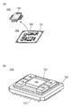
- FIGS. 31A and 31B are diagrams illustrating electronic components.
- FIG. 32 is a diagram illustrating an electronic device.
- FIGS. 33A to 33E are diagrams illustrating electronic devices.
- FIGS. 34A to 34C are diagrams illustrating electronic devices.
- FIGS. 35A to 35C are diagrams illustrating electronic devices.
- FIG. 36 is a diagram illustrating various storage devices for each hierarchy.
- FIG. 37 is a diagram showing the data write time and write durability of various storage devices.
- FIG. 38 is a diagram illustrating data retention times and operating
- H level also referred to as “VDD” or “H potential”
- L level also referred to as “VSS” or “L potential”.
- a voltage refers to a potential difference between two points, and a potential refers to electrostatic energy (electric potential energy) of a unit charge in an electrostatic field at a certain point.
- a potential difference between a potential at a certain point and a reference potential is simply referred to as a potential or a voltage, and the potential and the voltage are often used as synonyms.
- a potential may be read as a voltage or a voltage may be read as a potential unless otherwise specified.
- a metal oxide is a metal oxide in a broad sense. Metal oxides are classified into oxide insulators, oxide conductors (including transparent oxide conductors), oxide semiconductors, and the like. For example, in the case where a metal oxide is used for a semiconductor layer of a transistor, the metal oxide may be referred to as an oxide semiconductor in some cases.
- the term “OS transistor” can be referred to as a transistor including a metal oxide or an oxide semiconductor.
- a metal oxide containing nitrogen may be collectively referred to as a metal oxide.
- the threshold voltage (also referred to as “Vth”) is higher than 0V.
- Embodiment 1 In Embodiment, a storage device according to one embodiment of the present invention will be described.
- FIG. 1 is a block diagram illustrating a configuration example of a storage device.
- the storage device 100 includes a peripheral circuit 111 and a cell array 201.
- the peripheral circuit 111 includes a row decoder 121, a word line driver circuit 122, a column decoder 131, a bit line driver circuit 130, an output circuit 140, and a control logic circuit 160.
- the cell array 201 has memory cells 211, word lines WWL, word lines RWL, bit lines WBL, and bit lines RBL.
- the word line driver circuit 122 has a function of supplying a potential to the word line WWL and the word line RWL.
- the bit line driver circuit 130 has a precharge circuit 132, an amplifier circuit 133, and an input / output circuit 134.
- the precharge circuit 132 has a function of precharging the bit line RBL and the like.
- the amplifier circuit 133 has a function of amplifying a data signal read from the wiring RBL.
- the word lines WWL, word lines RWL, bit lines WBL, and bit lines RBL are wirings connected to the memory cells 211, and will be described later in detail.
- the amplified data signal is output to the outside of the storage device 100 as a digital data signal RDATA via the output circuit 140.
- VDD and VSS are externally supplied to the storage device 100 as power supply potentials.
- a clock signal CLK a chip enable signal CE, a write enable signal WE, a read enable signal RE, an address signal ADDR, a data signal WDATA, and the like are externally input to the storage device 100.
- the address signal ADDR is input to the row decoder 121 and the column decoder 131, and the data signal WDATA is input to the input / output circuit 134.
- the control logic circuit 160 processes the chip enable signal CE, the write enable signal WE, and the read enable signal RE to generate control signals for the row decoder 121 and the column decoder 131. For example, when the chip enable signal CE is at a high level and the write enable signal WE is at a low level, the row decoder 121 and the column decoder 131 perform a read operation, and when the chip enable signal CE is at a high level and the write enable signal WE is at a high level.
- the row decoder 121 and the column decoder 131 perform a write operation, and when the chip enable signal CE is at a low level, the row decoder 121 and the column decoder 131 perform a standby operation regardless of the high level and the low level of the write enable signal WE. be able to.
- control logic circuit 160 signals processed by the control logic circuit 160 are not limited to these. Other signals may be input to the control logic circuit 160 as needed.
- An OS transistor can be used as a transistor included in the cell array 201. Further, an OS transistor can be used as a transistor included in the peripheral circuit 111. By forming the cell array 201 and the peripheral circuit 111 using OS transistors, the cell array 201 and the peripheral circuit 111 can be manufactured in the same manufacturing process, so that manufacturing cost can be reduced.
- OS transistor can be applied not only to a memory device but also to a logic circuit represented by a CPU (Central Processing Unit) or a GPU (Graphics Processing Unit).
- CPU Central Processing Unit
- GPU Graphics Processing Unit
- a general term for an integrated circuit using OS transistors is also referred to as “OS-LSI”.
- FIG. 2A illustrates details of the cell array 201.
- the cell array 201 includes m (m is an integer of 1 or more) pieces in one column and n (n is an integer of 1 or more) pieces in one row, and a total of m ⁇ n memory cells 211, and The cells 211 are arranged in a matrix.
- the address of the memory cell 211 is also shown.
- [1, 1] indicates the memory cell 211 located at the address of the first row and the first column
- [i, j] (i is an integer of 1 or more and m or less, and j is 1 or more and n
- the following integer indicates a memory cell 211 located at the address of the i-th row and the j-th column.
- the number of wirings connecting the cell array 201 and the word line driver circuit 122 is determined by the configuration of the memory cells 211, the number of memory cells 211 included in one column, and the like.
- the number of wirings connecting the cell array 201 and the bit line driver circuit 130 is determined by the configuration of the memory cells 211, the number of memory cells 211 included in one row, and the like.
- the cell array 201 includes n bit lines WBL (WBL [1] to WBL [n]), n bit lines RBL (RBL [1] to RBL [n]), and m words. It has a line WWL (WWL [1] to WWL [m]) and m word lines RWL (RWL [1] to RWL [m]).
- Memory cell 211 is connected to bit line WBL, bit line RBL, word line WWL, and word line RWL. As shown in FIG. 2A, a memory cell 211 whose address is [i, j] is electrically connected to a word line driver circuit 122 via a word line WWL [i] and a word line RWL [i]. , Bit line driver circuit 130 via bit line WBL [j] and bit line RBL [j].
- FIGS. 2B and 2C and FIGS. 5A to 5D illustrate circuit configuration examples applicable to the memory cell 211.
- FIG. FIG. 2B illustrates a circuit configuration example of a gain cell (also referred to as “2Tr1C”) memory cell 211A including two transistors and one capacitor.
- the memory cell 211A includes a transistor M11, a transistor M12, and a capacitor Cs.
- one of the source and the drain of the transistor M11 is electrically connected to the first terminal of the capacitor Cs and the gate of the transistor M12, and the other of the source and the drain of the transistor M11 is electrically connected to the bit line WBL.
- the gate of the transistor M11 is electrically connected to the word line WWL.
- One of a source and a drain of the transistor M12 is electrically connected to the word line RWL, and the other of the source and the drain of the transistor M12 is electrically connected to the bit line RBL.
- the second terminal of the capacitor Cs is electrically connected to the wiring CAL.
- the wiring CAL functions as a wiring for applying a predetermined potential to the second terminal of the capacitor Cs.
- a node at which one of the source and the drain of the transistor M11, the first terminal of the capacitor Cs, and the gate of the transistor M12 are electrically connected is referred to as a node SN.
- the bit line WBL functions as a write bit line
- the bit line RBL functions as a read bit line
- the word line WWL functions as a write word line
- the word line RWL functions as a read word line.
- the transistor M11 has a function as a switch for turning on or off the node SN and the bit line WBL.
- FIG. 3 is a timing chart for explaining the operation of the memory cell 211A.
- VDD is applied to the word line WWL to make the transistor M11 conductive (also referred to as an “on state”), and the node SN is electrically connected to the bit line WBL. It is done by doing.
- the potential of the word line RWL is set to VDD. Further, it is preferable that the potential of the bit line RBL is also set to VDD.
- VDD a potential corresponding to data to be written
- Vdata data to be written
- VSS is applied to the word line WWL to turn off the transistor M11 (also referred to as an “off state”), so that the potential of the node SN is held.
- a parasitic capacitance Cz is generated between the gate of the transistor M11 and one of the source and the drain of the transistor M11.
- the word line WWL and the node SN are capacitively coupled via a parasitic capacitance Cz. Therefore, when the potential of the word line WWL is reduced from VDD to VSS at the end of the write operation, the potential of the node SN decreases by the voltage ⁇ V1.
- the voltage ⁇ V1 is determined by the ratio of the parasitic capacitance Cz to the capacitance Csn.
- the voltage ⁇ V1 can be reduced as the capacitance Csn is larger than the parasitic capacitance Cz.
- the capacitance Csn includes a parasitic capacitance Cx generated at the node SN and the gate capacitance of the transistor M12. By increasing the gate capacitance of the transistor M12, the capacitance Csn can be increased.
- the capacitance value of the parasitic capacitance Cz is proportional to the gate capacitance of the transistor M11. Particularly, it is proportional to the channel width of the transistor M11.
- the capacitance of the capacitance Csn is dominated by the gate capacitance of the transistor M12. In this case, the voltage ⁇ V1 can be reduced by making the gate capacitance of the transistor M12 larger than the gate capacitance of the transistor M11.
- a predetermined potential is applied to the bit line RBL in a data reading period (Tread), and thereafter, the bit line RBL is electrically floated, and then a low-level potential is applied to the word line RWL. This is done by applying.
- applying a predetermined potential to the bit line RBL and then bringing the bit line RBL into a floating state is referred to as precharging the bit line RBL.
- VDD is precharged to the bit line RBL, and then VSS is applied to the word line RWL.
- VSS is applied to the word line RWL.
- the potential difference between the node SN and the word line RWL is equal to or higher than the threshold voltage of the transistor M12, the potential of the bit line RBL decreases at a speed corresponding to the potential difference. That is, by knowing the potential change of the bit line RBL, the potential held at the node SN can be read.
- the row where the memory cells 211A to which data is written is selected by the word line WWL to which VDD is applied, and the row where the memory cells 211 to read data are arranged is selected by the word line RWL to which VSS is applied. Is done. Conversely, the row in which the memory cells 211 to which data is not written is arranged is applied with VSS to the word line WWL, and the row in which the memory cells 211A from which data is not read is arranged is set to the word line RWL and the bit line RBL. By applying a potential higher than the potential to be precharged, non-selection can be performed.
- a transistor including a metal oxide in a channel formation region can be used.
- OS transistor a transistor including a metal oxide in a channel formation region
- indium an element M (the element M is aluminum, gallium, yttrium, copper, vanadium, beryllium, boron, titanium, iron, nickel, germanium, zirconium, molybdenum, lanthanum, Metal oxide containing any one of cerium, neodymium, hafnium, tantalum, tungsten, magnesium, or the like) or zinc can be used.
- a metal oxide composed of indium, gallium, and zinc is preferable.
- the off-state current of the OS transistor is extremely small; therefore, by using the OS transistor as the transistor M11, the potential written to the node SN can be held for a long time. That is, data written to the memory cell 211A can be held for a long time.
- transistor M12 there is no particular limitation on the transistor used as the transistor M12.
- the transistor M12 an OS transistor, a Si transistor, or another transistor may be used.
- silicon used for a semiconductor layer in which a channel is formed includes amorphous silicon, polycrystalline silicon, low-temperature polysilicon (LTPS), single-crystal silicon, or low-temperature polysilicon. do it. Since the Si transistor has higher field-effect mobility than the OS transistor in some cases, the use of a Si transistor as the reading transistor can increase the operation speed in reading.
- an OS transistor is used as the transistor M11 and a Si transistor is used as the transistor M12, both may be stacked in different layers.
- the OS transistor can be manufactured using a manufacturing device and a process similar to those of the Si transistor. Therefore, it is easy to mix (hybridize) the OS transistor and the Si transistor, and it is easy to achieve high integration.
- an OS transistor when used as the transistor M12, leakage current can be extremely reduced when not selected, so that reading accuracy can be improved.
- an OS transistor for both the transistor M11 and the transistor M12, the number of manufacturing steps of a semiconductor device can be reduced, so that productivity can be increased.
- a semiconductor device can be manufactured at a process temperature of 400 ° C. or lower.
- NOSRAM Non-volatile Oxide Semiconductor Semiconductor Random Access Memory
- the memory cell 211A is a 2Tr1C type memory cell.
- the memory cell 211A can operate as a memory by amplifying the accumulated charge with the transistor M12 even when the capacitor Cs for accumulating charge is small.
- the off-state current of the OS transistor is extremely small; therefore, by using the OS transistor as the transistor M11, the capacitor Cs can be reduced or eliminated.
- FIG. 2C illustrates a circuit configuration example of a DRAM (Dynamic Random Access Memory) memory cell 211R including one transistor and one capacitor.
- the memory cell 211R includes a transistor M11 and a capacitor Cs.
- one of the source and the drain of the transistor M11 is electrically connected to the first terminal of the capacitor Cs, and the other of the source and the drain of the transistor M11 is electrically connected to the bit line BL.
- the gate is electrically connected to the word line WL.
- the second terminal of the capacitor Cs is electrically connected to the wiring CAL.
- the wiring CAL functions as a wiring for applying a predetermined potential to the second terminal of the capacitor CS.
- a node at which one of the source and the drain of the transistor M11 and the first terminal of the capacitor Cs are electrically connected is referred to as a node SN.
- the capacitor Cs can be reduced or eliminated. Further, since the written data can be held for a long time by the transistor M11, the refresh frequency of the DRAM memory cell can be reduced. Further, the refresh operation of the DRAM type memory cell can be made unnecessary.
- DOSRAM Dynamic Oxide Semiconductor Semiconductor Random Access Memory
- the area occupied by the memory cell can be reduced. Therefore, miniaturization or high integration of the storage device is easy.
- FIGS. 4A and 4B illustrate an example of an Id-Vg characteristic which is one of electric characteristics of a transistor.
- the Id-Vg characteristic indicates a change in drain current (Id) with respect to a change in gate voltage (Vg).
- the horizontal axis in FIGS. 4A and 4B indicates Vg on a linear scale.
- the vertical axes in FIGS. 4A and 4B indicate Id on a log scale.
- FIG. 4A illustrates the Id-Vg characteristics of the OS transistor.
- FIG. 4B illustrates the Id-Vg characteristics of a transistor in which silicon is used for a semiconductor layer in which a channel is formed (also referred to as a “Si transistor” or a “Si-FET”).
- 4A and 4B show the Id-Vg characteristics of an n-channel transistor.
- the off-state current of the OS transistor does not easily increase even in an operation in a high-temperature environment.
- the OS transistor can achieve an on / off ratio of 10 digits or more even when the operating temperature is 125 ° C. to 150 ° C.
- Vth shifts in the negative direction with an increase in temperature, and the on-current increases. Therefore, the frequency characteristic tends to increase as the operating temperature increases.
- the off-state current of the Si transistor increases as the temperature increases. In the Si transistor, Vth shifts in the positive direction as the temperature increases, and the on-current decreases.
- an operating frequency of 200 MHz or more can be realized in a case where the driving voltage is 2.5 V and the operating temperature is in a range of ⁇ 40 ° C. to 85 ° C., for example.
- FIG. 5A illustrates a circuit configuration example of the memory cell 211 in which the capacitor Cs is not provided.
- the memory cell 211B illustrated in FIG. 5A has a circuit configuration in which the capacitor Cs is removed from the memory cell 211A.
- the charge (potential) written to the node SN is mainly held by the gate capacitance of the transistor M12 and the parasitic capacitance Cx. Note that the gate capacitance can also be considered as a part of the parasitic capacitance Cx.
- a transistor having a back gate may be used as one or both of the transistor M11 and the transistor M12.
- a gate and a back gate are provided so as to overlap with each other via a channel formation region of a semiconductor layer. Both the gate and the back gate can function as gates. Therefore, when one is called “back gate”, the other is sometimes called “gate” or “front gate”. Also, one may be referred to as a “first gate” and the other as a “second gate”.
- the back gate may have the same potential as the gate, a ground potential, or an arbitrary potential. Further, the threshold voltage of the transistor can be changed by changing the potential of the back gate independently without interlocking with the gate.
- the back gate When the back gate is provided and the gate and the back gate are set at the same potential, the region where carriers flow in the semiconductor layer becomes larger in the film thickness direction, so that the amount of carrier movement increases. As a result, the on-state current of the transistor increases and the field-effect mobility increases.
- the transistor can have high on-state current with respect to the occupied area. That is, the area occupied by the transistor can be reduced with respect to the required on-state current. Thus, a highly integrated semiconductor device can be realized.
- FIGS. 5B to 5D illustrate circuit configuration examples in the case where a transistor having a back gate (a four-terminal transistor; also referred to as a “four-terminal element”) is used as the transistors M11 and M12.
- a memory cell 211C illustrated in FIG. 5B, a memory cell 211D illustrated in FIG. 5C, and a memory cell 211E illustrated in FIG. 5D are modifications of the memory cell 211B.
- the gate and the back gate of the transistor M11 are electrically connected. Further, the gate and the back gate of the transistor M12 are electrically connected.
- the back gate of the transistor M11 and the back gate of the transistor M12 are electrically connected to the wiring BGL.
- a predetermined potential can be applied to the back gates of the transistors M11 and M12 through the wiring BGL.
- the threshold voltage of the transistor M11 and the transistor M12 can be changed depending on the potential of the wiring BGL. Specifically, by increasing the potential applied to the back gates of the transistor M11 and the transistor M12, the respective threshold voltages shift to minus. When the threshold voltage shifts in the negative direction, the on-state current of the transistor can be increased and the operation speed of the memory cell 211D can be increased.
- the respective threshold voltages shift to plus.
- the threshold voltage shifts to a positive value off-state current of the transistor is reduced, and data written in the memory cell 211D can be held for a long time.
- the back gate of the transistor M11 is electrically connected to the wiring WBGL
- the back gate of the transistor M12 is electrically connected to the wiring RBGL.
- a storage device including the memory cells 211B to 211E can also be referred to as a NOSRAM.
- MRAM Magneticoresistive Random Access Memory
- ReRAM Resistive Memory Controller
- MTJ Magnetic Tunnel Junction
- phase-change memory Phase-change memory
- the memory device of one embodiment of the present invention is characterized by being excellent in repetitive rewriting durability and having little structural change because it operates by charge or discharge through a transistor when information is rewritten.
- the node SN is easily affected by noise. Specifically, due to the capacitive coupling between the node SN and the adjacent memory cell, the influence of the potential change of the adjacent memory cell is increased. As a result, the data retention time is shortened, the reading accuracy is reduced, and the like, and the reliability of the storage device is reduced.
- the reduction of the noise can be realized by reducing the parasitic capacitance generated between adjacent memory cells.
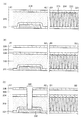
- a region with a low relative dielectric constant (LDR: Low ⁇ Constant ⁇ Region) is provided outside a memory cell in order to reduce parasitic capacitance between adjacent memory cells.
- the relative permittivity of the LDR may be smaller than the relative permittivity of the adjacent insulating layer.
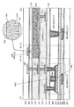
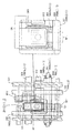
- FIG. 5E an LDR 221 is provided outside the memory cell 211E.
- FIG. 6 shows an example of the arrangement of the memory cells 211 [i, j] to 211 [i + 1, j + 2] arranged in a matrix and the LDR 221 shown in FIG. 5E. Note that in FIG. 6, the memory cell 211E illustrated in FIG. 5D is used as the memory cell 211.
- FIG. 7 shows a modification of FIG. As shown in FIG. 7, some LDRs 221 may be connected and provided.
- the LDR 221 illustrated in FIG. 7 has a region extending along a word line and a region extending along a bit line.
- FIG. 8 illustrates an example of the arrangement of the memory cells 211 [i, j] to 211 [i + 1, j + 2] arranged in a matrix and the LDR 221 illustrated in FIG. 5F.
- a memory cell 211E is used as the memory cell 211.
- the LDR 221 shown in FIG. 8 also has a region extending along a word line and a region extending along a bit line.
- the influence of noise can be reduced and the reliability of the storage device can be increased.
- This embodiment can be implemented in appropriate combination with the structures described in the other embodiments and the like.
- FIG. 9 illustrates a planar configuration example of the memory cells 211 [i, j] to 211 [i + 1, j + 2] arranged in a matrix.
- FIG. 9 is a plan configuration example corresponding to the circuit diagram shown in FIG.
- two adjacent memory cells 211 are arranged to be mirror symmetric.
- the memory cell 211 [i, j] and the memory cell 211 [i, j + 1] are mirror symmetric.
- the memory cell 211 [i, j] and the memory cell 211 [i + 1, j] are also mirror-symmetric.
- FIG. 10A shows a planar configuration example of the memory cell 211 [i + 1, j] in FIG.
- One of a source and a drain of the transistor M11 is electrically connected to the conductive layer 360 through the electrode 341.
- the conductive layer 360 functions as a gate electrode of the transistor M12.
- a region including the electrode 341 and the conductive layer 360 functions as a node SN.
- the other of the source and the drain of the transistor M11 is electrically connected to the conductive layer 339.
- Conductive layer 339 functions as bit line WBL.
- One of a source and a drain of the transistor M12 is electrically connected to the conductive layer 333 through the conductive layer 312, and the other of the source and the drain of the transistor M12 is electrically connected to the conductive layer 338.
- Conductive layer 333 functions as word line RWL
- conductive layer 338 functions as bit line RBL.
- the conductive layer 305 illustrated in FIG. 10A functions as a wiring RBGL, and the conductive layer 306 functions as a wiring WBGL.
- the conductive layer 261 functions as a word line WWL, and the conductive layer 333 functions as a word line RWL.
- Part of the conductive layer 305 functions as a back gate electrode of the transistor M12.
- Part of the conductive layer 306 functions as a back gate electrode of the transistor M11.
- LDR 221 has a region extending along bit line RBL (conductive layer 338) and a region extending along word line RWL.
- the capacitor Cs is not provided; therefore, the area occupied by the memory cell 211 can be reduced.
- the occupied area is small, it is easily affected by noise generated from adjacent memory cells and the like.
- noise transmitted to the node SN can be reduced.
- the gate capacitance of the transistor M12 may be increased by increasing the overlapping area of the semiconductor layer 260 and the conductive layer 360 of the transistor M12. Further, the increase in the gate capacitance of the transistor M12 is effective in improving the potential drop of the node SN which occurs at the end of the write operation.
- the area where the semiconductor layer and the gate electrode of the transistor M12 overlap is preferably 1 to 5 times, more preferably 1 to 10 times, and more preferably 1 to 10 times the area where the semiconductor layer and the gate electrode of the transistor M11 overlap. More preferably, it is more than 50 times.
- FIG. 11 is a diagram showing an example of a cross-sectional configuration of the A1-A2 site, the B1-B2 site, and the C1-C2 site indicated by the alternate long and short dash line in FIG.
- a transistor M12 is provided over a substrate 301.
- the transistor M11 can have a stacked structure similar to that of the transistor M12.
- An insulating layer 309 and an insulating layer 326 are provided over a substrate 301, and a conductive layer 305 and a conductive layer 306 are embedded in the insulating layer 326.
- the insulating layer 322 and the insulating layer 324 are provided over the insulating layer 326, and the semiconductor layer 260 is provided over the insulating layer 324.
- the insulating layer 354 and the insulating layer 380 are provided over the insulating layer 324 and the semiconductor layer 260. Further, the conductive layer 360 and the conductive layer 261 are embedded in the insulating layer 380. An insulating layer 374 is provided over the insulating layer 380, the conductive layer 360, and the conductive layer 261, and an insulating layer 381 is provided over the insulating layer 374.
- a conductive layer 312, a conductive layer 313, and a conductive layer 314 are provided over the insulating layer 381.
- the conductive layer 312 is electrically connected to one of the source and the drain of the transistor M12, and the conductive layer 313 is electrically connected to the other of the source and the drain of the transistor M12.
- the insulating layer 311 and the insulating layer 315 are provided over the insulating layer 381, the conductive layer 312, the conductive layer 313, and the conductive layer 314.
- the conductive layer 332 and the conductive layer 333 are provided over the insulating layer 315.
- the conductive layer 332 is electrically connected to the conductive layer 313 through the contact plug 317
- the conductive layer 333 is electrically connected to the conductive layer 314 through the contact plug 318.
- An insulating layer 331, an insulating layer 319, and an insulating layer 334 are provided over the insulating layer 315, the conductive layer 332, and the conductive layer 333.
- the LDR 221 is provided in a part of the insulating layer 319.
- the LDR 221 includes a plurality of LDSs 235 (Low dielectric constant space: Low dielectric constant). The LDR 221 and LDS 235 will be described later.
- An insulating layer 334 is provided over the insulating layer 319 and the LDS 235.
- An insulating layer 335 and an insulating layer 336 are provided over the insulating layer 334.
- a conductive layer 338 is provided over the insulating layer 336, and the conductive layer 338 is electrically connected to the conductive layer 332 through a contact plug 337.
- the insulating layer 343 is provided over the insulating layer 336 and the conductive layer 338.
- FIG. 12 is a diagram illustrating a planar configuration example of the memory cell 211 [i + 1, j].
- FIG. 13 is a diagram illustrating a cross-sectional configuration example of a G1-G2 portion indicated by a dashed line in FIG.
- one of the source and the drain of the transistor M11, the conductive layer 341 and the conductive layer 306 are provided so as to overlap as much as possible. With this configuration, the parasitic capacitance Cx related to the node SN can be increased without providing the capacitor Cs.
- the conductive layer 306 is hatched in order to clearly show the conductive layer 306.
- the conductive layer 306 can be formed at the same time using the same material and the same method as the conductive layer 305 without hatching.
- the area of the conductive layer 306 and the memory cell 211 [i + 1, j] may be increased by increasing the area of the conductive layer 306.
- the area of the conductive layer 305 overlapping the node SN may be increased to increase the parasitic capacitance Cx related to the node SN.
- part of the conductive layer 305 is modified so that one of the source and the drain of the transistor M11, the conductive layer 341 and the conductive layer 305 overlap with each other as much as possible.
- the parasitic capacitance Cx related to the node SN can be increased without providing the capacitor Cs.
- the conductive layer 305 is hatched in order to clearly show the conductive layer 305.
- the conductive layer 305 can be formed at the same time using the same material and the same method as the conductive layer 306 without hatching.
- the area of the conductive layer 305 and the memory cell 211 [i + 1, j] may be increased by increasing the area of the conductive layer 305.
- ⁇ substrate ⁇ There is no particular limitation on the material used for the substrate.
- an insulator substrate, a semiconductor substrate, or a conductor substrate may be used.
- the insulator substrate examples include a glass substrate, a quartz substrate, a sapphire substrate, a stabilized zirconia substrate (such as a yttria-stabilized zirconia substrate), and a resin substrate.
- the semiconductor substrate examples include a semiconductor substrate formed using silicon, germanium, or the like, or a compound semiconductor substrate formed using silicon carbide, silicon germanium, gallium arsenide, indium phosphide, zinc oxide, or gallium oxide.
- a semiconductor substrate having an insulator region inside the above-described semiconductor substrate, for example, an SOI (Silicon On Insulator) substrate may be used.
- the conductor substrate examples include a graphite substrate, a metal substrate, an alloy substrate, and a conductive resin substrate.
- a substrate including a metal nitride, a substrate including a metal oxide, and the like can be given.
- a substrate in which an element is provided may be used.
- Elements provided on the substrate include a capacitor, a resistor, a switch, a light-emitting element, a storage element, and the like.
- a semiconductor substrate provided with a semiconductor element such as a strained transistor or a FIN transistor on a semiconductor substrate can also be used. That is, the substrate is not limited to a mere support substrate, and may be a substrate on which devices such as other transistors are formed.
- Insulating layer examples of a material used for the insulating layer include an oxide, a nitride, an oxynitride, a nitrided oxide, a metal oxide, a metal oxynitride, and a metal nitrided oxide having an insulating property.
- a problem such as leakage current may occur due to a reduction in the thickness of a gate insulating layer.
- a high-k material for the insulating layer functioning as a gate insulating layer voltage reduction during transistor operation can be achieved while the physical thickness is maintained.
- a material having a low relative dielectric constant for an insulator functioning as an interlayer insulating layer parasitic capacitance generated between wirings can be reduced. Therefore, a material may be selected according to the function of the insulating layer.
- Examples of the insulator having a high relative dielectric constant include gallium oxide, hafnium oxide, zirconium oxide, an oxide containing aluminum and hafnium, an oxynitride containing aluminum and hafnium, an oxide containing silicon and hafnium, and silicon and hafnium. Oxynitride or nitride containing silicon and hafnium.
- Examples of the insulator having a low relative dielectric constant include silicon oxide, silicon oxynitride, silicon nitride oxide, silicon nitride, silicon oxide added with fluorine, silicon oxide added with carbon, silicon oxide added with carbon and nitrogen, and empty. There is silicon oxide having a hole, resin, or the like.
- the transistor is formed using an insulating layer (an insulating layer 309, an insulating layer 322, an insulating layer 354, an insulating layer 374, or the like) having a function of suppressing transmission of impurities such as hydrogen and oxygen.
- an insulating layer an insulating layer 309, an insulating layer 322, an insulating layer 354, an insulating layer 374, or the like
- the electrical characteristics of the transistor can be stabilized.
- the insulator having a function of suppressing the transmission of impurities such as hydrogen and oxygen include boron, carbon, nitrogen, oxygen, fluorine, magnesium, aluminum, silicon, phosphorus, chlorine, argon, gallium, germanium, yttrium, and zirconium.
- Lanthanum, neodymium, hafnium, or an insulator containing tantalum may be used as a single layer or a stacked layer.
- an insulator having a function of suppressing transmission of impurities such as hydrogen and oxygen
- a metal oxide such as tantalum oxide, a metal nitride such as aluminum nitride, aluminum titanium nitride, titanium nitride, silicon nitride oxide, or silicon nitride can be used.
- the insulating layer functioning as a gate insulating layer is preferably an insulator having a region containing oxygen released by heating.
- an insulator having a region containing oxygen released by heating For example, with a structure in which silicon oxide or silicon oxynitride having a region containing oxygen released by heating is in contact with the semiconductor layer 260, oxygen vacancies in the semiconductor layer 260 can be compensated.
- a nitrided oxide refers to a compound having a higher nitrogen content than oxygen.
- Oxynitride refers to a compound having a higher oxygen content than nitrogen.
- the content of each element can be measured, for example, by using Rutherford Backscattering (RBS) or Spectrometry (RBS).
- the concentration of hydrogen in the insulating layer is preferably reduced in order to prevent an increase in the concentration of hydrogen in the semiconductor layer.
- the concentration of hydrogen in the insulating layer is determined to be 2 ⁇ 10 20 atoms / cm 3 or less, preferably 5 ⁇ 10 19 atoms / cm 3 or less by secondary ion mass spectrometry (SIMS). It is more preferably at most 1 ⁇ 10 19 atoms / cm 3 , further preferably at most 5 ⁇ 10 18 atoms / cm 3 .
- SIMS secondary ion mass spectrometry
- the concentration of nitrogen in the insulating layer is preferably reduced in order to prevent an increase in the concentration of nitrogen in the semiconductor layer.
- the concentration of nitrogen in the insulating layer is set to 5 ⁇ 10 19 atoms / cm 3 or less, preferably 5 ⁇ 10 18 atoms / cm 3 or less, more preferably 1 ⁇ 10 18 atoms / cm 3 or less in SIMS. More preferably, it is set to 5 ⁇ 10 17 atoms / cm 3 or less.
- the region is observed by an electron spin resonance (ESR) method.
- ESR electron spin resonance
- the number of signals is small.
- the above signal includes the E ′ center where the g value is observed at 2.001.
- the E ′ center is caused by dangling bonds of silicon.
- the spin density attributable to the E ′ center is 3 ⁇ 10 17 spins / cm 3 or less, preferably 5 ⁇ 10 16 spins / cm 3 or less.
- a silicon oxide layer or a silicon oxynitride layer may be used.
- a signal due to nitrogen dioxide (NO 2 ) may be observed in addition to the above signal.
- the signal is split into three signals by the nuclear spin of N, and each g value is 2.037 or more and 2.039 or less (hereinafter referred to as a first signal), and 2.001 or more and 2.003 or less (first signal). 2) and 1.964 to 1.966 (third signal).
- the insulating layer an insulating layer in which the spin density of a signal due to nitrogen dioxide (NO 2 ) is greater than or equal to 1 ⁇ 10 17 spins / cm 3 and less than 1 ⁇ 10 18 spins / cm 3 .
- NO 2 nitrogen dioxide
- nitrogen oxide (NO x ) containing nitrogen dioxide (NO 2 ) forms a level in the insulating layer.
- the level is located in the energy gap of the oxide semiconductor layer. Therefore, when nitrogen oxide (NO x ) diffuses into the interface between the insulating layer and the oxide semiconductor layer, the level may trap electrons on the insulating layer side. As a result, the trapped electrons remain near the interface between the insulating layer and the oxide semiconductor layer, so that the threshold voltage of the transistor is shifted in the positive direction. Therefore, when a film having a low content of nitrogen oxide is used as the insulating layer and the insulating layer, a shift in threshold voltage of the transistor can be reduced.
- a silicon oxynitride layer can be used as the insulating layer from which the amount of released nitrogen oxides (NO x ) is small.
- the silicon oxynitride layer is a film which emits more ammonia than nitrogen oxide (NO x ) in thermal desorption spectroscopy (TDS), and typically, ammonia.
- TDS thermal desorption spectroscopy
- the release amount is 1 ⁇ 10 18 / cm 3 or more and 5 ⁇ 10 19 / cm 3 or less. Note that the above-mentioned amount of released ammonia is the total amount in the range where the temperature of the heat treatment in TDS is 50 ° C or more and 650 ° C or less, or 50 ° C or more and 550 ° C or less.
- nitrogen oxide (NO x ) reacts with ammonia and oxygen in heat treatment, nitrogen oxide (NO x ) is reduced by using an insulating layer from which a large amount of ammonia is released.
- At least one of the insulating layers in contact with the oxide semiconductor layer is preferably formed using an insulating layer from which oxygen is released by heating.
- the amount of desorbed oxygen converted to oxygen atoms is 1.0 ⁇ 10 18 atoms / cm 3 or more, it is preferable to use 1.0 ⁇ 10 19 atoms / cm 3 or more, or 1.0 ⁇ 10 insulating layer is 20 atoms / cm 3 or more. Note that in this specification and the like, oxygen released by heating is also referred to as “excess oxygen”.
- the insulating layer containing excess oxygen can be formed by performing treatment for adding oxygen to the insulating layer.
- the treatment for adding oxygen can be performed by heat treatment in an oxidizing atmosphere, plasma treatment, or the like.
- oxygen may be added by an ion implantation method, an ion doping method, a plasma immersion ion implantation method, or the like.
- a gas used for the treatment for adding oxygen a gas containing oxygen, such as an oxygen gas such as 16 O 2 or 18 O 2 , a nitrous oxide gas, or an ozone gas, can be given.
- the process of adding oxygen is also referred to as “oxygen doping process”.
- the oxygen doping treatment may be performed by heating the substrate.
- an organic material having heat resistance such as polyimide, an acrylic resin, a benzocyclobutene-based resin, polyamide, or an epoxy-based resin
- a low dielectric constant material low-k material
- a siloxane-based resin PSG (phosphorus glass), BPSG (phosphorus glass), or the like
- the insulating layer may be formed by stacking a plurality of insulating layers formed using these materials.
- a siloxane-based resin corresponds to a resin including a Si-O-Si bond formed using a siloxane-based material as a starting material.
- the siloxane-based resin may use an organic group (for example, an alkyl group or an aryl group) or a fluoro group as a substituent. Further, the organic group may have a fluoro group.
- the method for forming the insulating layer is not particularly limited. Note that a baking step may be required depending on a material used for the insulating layer. In this case, a transistor can be efficiently manufactured by combining the step of baking the insulating layer with another heat treatment step.
- the method for forming the insulating layer is not particularly limited. Note that a baking step may be required depending on a material used for the insulating layer. In this case, a transistor can be efficiently manufactured by combining the step of baking the insulating layer with another heat treatment step.
- (Conductive layer) Aluminum, chromium, copper, silver, gold, platinum, tantalum, nickel, titanium, molybdenum, tungsten, hafnium, vanadium, niobium, manganese, magnesium, zirconium, beryllium, indium, ruthenium, iridium, strontium, lanthanum It is preferable to use a metal element selected from the above, an alloy containing the above-described metal element as a component, an alloy in which the above-described metal elements are combined, or the like.
- tantalum nitride, titanium nitride, tungsten, a nitride containing titanium and aluminum, a nitride containing tantalum and aluminum, ruthenium oxide, ruthenium nitride, an oxide containing strontium and ruthenium, an oxide containing lanthanum and nickel, and the like are used. Is preferred.
- tantalum nitride, titanium nitride, nitride containing titanium and aluminum, nitride containing tantalum and aluminum, ruthenium oxide, ruthenium nitride, oxide containing strontium and ruthenium, and oxide containing lanthanum and nickel are not easily oxidized.
- a conductive material or a material which maintains conductivity even when oxygen is absorbed is preferable.
- a semiconductor having high electric conductivity represented by polycrystalline silicon containing an impurity element such as phosphorus, or a silicide such as nickel silicide may be used.
- a plurality of conductive layers formed using the above materials may be stacked.
- a stacked structure in which the above-described material containing a metal element and a conductive material containing oxygen are combined may be employed.
- a stacked structure in which the above-described material containing a metal element and a conductive material containing nitrogen are combined may be employed.
- a stacked structure of a combination of the above-described material containing a metal element, a conductive material containing oxygen, and a conductive material containing nitrogen may be used.
- the conductive layer serving as a gate electrode is a combination of the above-described material containing a metal element and a conductive material containing oxygen. It is preferable to use a laminated structure.
- a conductive material containing oxygen is preferably provided on the channel formation region side.
- a conductive material containing a metal element and oxygen contained in a metal oxide in which a channel is formed is preferably used.
- a conductive material containing the above-described metal element and nitrogen may be used.
- a conductive material containing nitrogen such as titanium nitride or tantalum nitride may be used.
- indium tin oxide ITO: Indium Tin Oxide
- indium oxide containing tungsten oxide indium zinc oxide containing tungsten oxide
- indium oxide containing titanium oxide indium tin oxide containing titanium oxide
- indium zinc Oxide and indium tin oxide to which silicon is added may be used.
- indium gallium zinc oxide containing nitrogen may be used.
- hydrogen contained in a metal oxide in which a channel is formed may be captured in some cases.
- hydrogen mixed in from an outer insulator or the like can be captured.
- a conductive material used for the contact plug and the like a conductive material having a high filling property such as tungsten or polysilicon may be used.
- a conductive material having a high filling property and a barrier layer (diffusion preventing layer) such as a titanium layer, a titanium nitride layer, or a tantalum nitride layer may be used in combination.
- semiconductor layer As the semiconductor layer, a single crystal semiconductor, a polycrystalline semiconductor, a microcrystalline semiconductor, an amorphous semiconductor, or the like can be used alone or in combination.
- semiconductor material for example, silicon, germanium, or the like can be used.
- a compound semiconductor such as silicon germanium, silicon carbide, gallium arsenide, an oxide semiconductor, a nitride semiconductor, or an organic semiconductor can be used.
- a low-molecular organic material having an aromatic ring, a ⁇ -electron conjugated conductive polymer, or the like can be used.
- a low-molecular organic material having an aromatic ring, a ⁇ -electron conjugated conductive polymer, or the like can be used.
- rubrene, tetracene, pentacene, perylene diimide, tetracyanoquinodimethane, polythiophene, polyacetylene, polyparaphenylene vinylene, and the like can be used.
- semiconductor layers may be stacked. In the case of stacking semiconductor layers, semiconductors having different crystal states may be used, or different semiconductor materials may be used.
- an oxide semiconductor which is one kind of metal oxide has a band gap of 2 eV or more; thus, when an oxide semiconductor is used for a semiconductor layer, a transistor with extremely low off-state current can be realized.
- an off-state current per 1 ⁇ m of channel width is less than 1 ⁇ 10 ⁇ 20 A and 1 ⁇ 10 ⁇ 22 A. Or less than 1 ⁇ 10 ⁇ 24 A. That is, the on / off ratio can be 20 digits or more.
- a transistor including an oxide semiconductor for a semiconductor layer (OS transistor) has high withstand voltage between a source and a drain.
- a highly reliable transistor can be provided.
- a transistor with a large output voltage and a high withstand voltage can be provided.
- a highly reliable storage device or the like can be provided.
- a storage device with a large output voltage and a high withstand voltage can be provided.
- a crystalline Si transistor can easily obtain a relatively higher mobility than an OS transistor.
- an OS transistor and a crystalline Si transistor may be used in combination depending on the purpose or application.
- the oxide semiconductor layer is preferably formed by a sputtering method.
- the oxide semiconductor layer is preferably formed by a sputtering method because the density of the oxide semiconductor layer can be increased.
- a rare gas typically, argon
- oxygen or a mixed gas of a rare gas and oxygen may be used as a sputtering gas. It is also necessary to increase the purity of the sputtering gas.
- an oxygen gas or a rare gas used as a sputtering gas a gas whose dew point is highly purified to -60 ° C or lower, preferably -100 ° C or lower is used.
- a highly purified sputtering gas deposition of moisture or the like into the oxide semiconductor layer can be prevented as much as possible.
- moisture in a deposition chamber included in the sputtering apparatus is preferably removed as much as possible.
- the deposition chamber be evacuated to a high vacuum (from about 5 ⁇ 10 ⁇ 7 Pa to about 1 ⁇ 10 ⁇ 4 Pa) using an adsorption-type vacuum exhaust pump such as a cryopump.
- Metal oxide By changing the composition of the element contained in the metal oxide, a conductor, a semiconductor, and an insulator can be separately formed.
- a metal oxide having physical properties of a conductor may be referred to as a “conductive oxide”.
- a metal oxide having semiconductor properties is sometimes referred to as an “oxide semiconductor”.
- a metal oxide having physical properties of an insulator may be referred to as an “insulating oxide”.
- An oxide semiconductor which is one kind of metal oxide preferably contains at least indium or zinc. In particular, it preferably contains indium and zinc. In addition, it is preferable that aluminum, gallium, yttrium, tin, or the like be contained in addition thereto. Further, one or more kinds selected from boron, silicon, titanium, iron, nickel, germanium, zirconium, molybdenum, lanthanum, cerium, neodymium, hafnium, tantalum, tungsten, magnesium, and the like may be included.
- the oxide semiconductor includes indium, the element M, and zinc is considered.
- the element M is aluminum, gallium, yttrium, tin, or the like.
- Other elements applicable to the element M include boron, silicon, titanium, iron, nickel, germanium, zirconium, molybdenum, lanthanum, cerium, neodymium, hafnium, tantalum, tungsten, and magnesium.
- a combination of a plurality of the aforementioned elements may be used as the element M.
- a metal oxide containing nitrogen may be collectively referred to as a metal oxide (metal oxide). Further, a metal oxide containing nitrogen may be referred to as metal oxynitride.
- An oxide semiconductor (metal oxide) is classified into a single crystal oxide semiconductor and a non-single-crystal oxide semiconductor.
- a non-single-crystal oxide semiconductor for example, a CAAC-OS, a polycrystalline oxide semiconductor, an nc-OS (nanocrystalline oxide semiconductor), a pseudo-amorphous oxide semiconductor (a-like OS: amorphous-like oxide semiconductor), And an amorphous oxide semiconductor.
- the CAAC-OS has a c-axis orientation and a crystal structure in which a plurality of nanocrystals are connected in an ab plane direction and has a strain.
- the strain refers to a region where the orientation of the lattice arrangement changes between a region where the lattice arrangement is uniform and a region where another lattice arrangement is uniform in a region where a plurality of nanocrystals are connected.
- the nanocrystal is based on a hexagon, but is not limited to a regular hexagon and may be a non-regular hexagon.
- distortion may have a lattice arrangement such as a pentagon and a heptagon.
- a clear crystal grain boundary also referred to as a grain boundary
- the CAAC-OS can tolerate distortion because the arrangement of oxygen atoms is not dense in the ab plane direction, or the substitution distance of a metal element changes the bonding distance between atoms. That's why.
- the CAAC-OS is a layered crystal in which a layer containing indium and oxygen (hereinafter, an In layer) and a layer containing elements M, zinc, and oxygen (hereinafter, an (M, Zn) layer) are stacked. It tends to have a structure (also called a layered structure).
- indium and the element M can be replaced with each other, and when the element M in the (M, Zn) layer is replaced with indium, it can also be referred to as an (In, M, Zn) layer. Further, when indium in the In layer is replaced with the element M, it can also be referred to as an (In, M) layer.
- CAAC-OS is a metal oxide with high crystallinity.
- the CAAC-OS it is difficult to confirm a clear crystal grain boundary; thus, it can be said that electron mobility due to the crystal grain boundary is hardly reduced.
- the CAAC-OS can be regarded as a metal oxide with few impurities and defects (such as oxygen vacancies). Therefore, a metal oxide having a CAAC-OS has stable physical properties. Therefore, a metal oxide including a CAAC-OS is resistant to heat and has high reliability.
- the nc-OS has a periodic atomic arrangement in a minute region (for example, a region with a thickness of 1 nm to 10 nm, particularly a region with a size of 1 nm to 3 nm).
- a minute region for example, a region with a thickness of 1 nm to 10 nm, particularly a region with a size of 1 nm to 3 nm.
- the nc-OS may not be distinguished from an a-like @ OS or an amorphous oxide semiconductor depending on an analysis method.
- an In—Ga—Zn oxide which is a kind of metal oxide containing indium, gallium, and zinc, may have a stable structure by being formed using the above-described nanocrystal. is there.
- IGZO tends to be difficult to grow in the air, it is preferable to use a smaller crystal (for example, the above-described nanocrystal) than a large crystal (here, a crystal of several mm or a crystal of several cm).
- a smaller crystal for example, the above-described nanocrystal
- a large crystal here, a crystal of several mm or a crystal of several cm.
- it may be structurally stable.
- a-like @ OS is a metal oxide having a structure between an nc-OS and an amorphous oxide semiconductor.
- a-like @ OS has voids or low density regions. That is, a-like @ OS has lower crystallinity than the nc-OS and the CAAC-OS.
- Oxide semiconductors have various structures, and each has different characteristics.
- the oxide semiconductor of one embodiment of the present invention may include two or more of an amorphous oxide semiconductor, a polycrystalline oxide semiconductor, an a-like @ OS, an nc-OS, and a CAAC-OS.
- the metal oxide for a channel formation region of the transistor, a transistor with high field-effect mobility can be realized. Further, a highly reliable transistor can be realized.
- a metal oxide having a low carrier density be used for the transistor.
- the impurity concentration in the metal oxide may be reduced and the density of defect states may be reduced.
- a low impurity concentration and a low density of defect states are referred to as high-purity intrinsic or substantially high-purity intrinsic.
- the metal oxide has a carrier density of less than 8 ⁇ 10 11 cm ⁇ 3 , preferably less than 1 ⁇ 10 11 cm ⁇ 3 , more preferably less than 1 ⁇ 10 10 cm ⁇ 3 , and 1 ⁇ 10 ⁇ 9 cm ⁇ 3. It may be set to ⁇ 3 or more.
- a highly purified intrinsic or substantially highly purified intrinsic metal oxide has a low defect state density, so that the trap state density may be low in some cases.
- the charge trapped in the trap level of the metal oxide takes a long time to disappear, and may behave as if it were a fixed charge. Therefore, a transistor including a metal oxide with a high trap state density in a channel formation region may have unstable electric characteristics in some cases.
- the impurities include hydrogen, nitrogen, an alkali metal, an alkaline earth metal, iron, nickel, and silicon.
- the concentration of the alkali metal or an alkaline earth metal in the metal oxide obtained by SIMS is set to 1 ⁇ 10 18 atoms / cm 3 or less, preferably 2 ⁇ 10 16 atoms / cm 3 or less.
- hydrogen contained in a metal oxide reacts with oxygen bonded to a metal atom to become water, which may form an oxygen vacancy. If oxygen vacancies are contained in the channel formation region in the metal oxide, the transistor tends to have normally-on characteristics. Furthermore, when hydrogen enters the oxygen vacancy, electrons serving as carriers may be generated. In addition, part of hydrogen may be bonded to oxygen which is bonded to a metal atom to generate an electron serving as a carrier. Therefore, a transistor including a metal oxide containing hydrogen is likely to have normally-on characteristics.
- the hydrogen concentration obtained by SIMS is less than 1 ⁇ 10 20 atoms / cm 3 , preferably less than 1 ⁇ 10 19 atoms / cm 3 , and more preferably 5 ⁇ 10 18 atoms / cm 3. It is less than 3 and more preferably less than 1 ⁇ 10 18 atoms / cm 3 .
- a thin film with high crystallinity As the metal oxide used for the semiconductor of the transistor. With the use of the thin film, stability or reliability of the transistor can be improved.
- the thin film include a single crystal metal oxide thin film and a polycrystalline metal oxide thin film.
- forming a thin film of a single crystal metal oxide or a thin film of a polycrystalline metal oxide on a substrate requires a high-temperature or laser heating step. Therefore, the cost of the manufacturing process increases, and the throughput also decreases.
- CAAC-IGZO In-Ga-Zn oxide having a CAAC structure
- nc-IGZO In-Ga-Zn oxide having an nc structure
- Non-Patent Document 3 it has been reported that nc-IGZO has periodicity in the atomic arrangement in a minute region (for example, a region of 1 nm or more and 3 nm or less) and that there is no regularity in crystal orientation between different regions. I have.
- Non-Patent Documents 4 and 5 show changes in the average crystal size due to the irradiation of an electron beam to each of the thin films of CAAC-IGZO, nc-IGZO, and IGZO having low crystallinity.
- a completely amorphous structure completely amorphous structure
- the CAAC-IGZO thin film and the nc-IGZO thin film have higher stability to electron beam irradiation than the IGZO thin film having low crystallinity. Therefore, it is preferable to use a thin film of CAAC-IGZO or a thin film of nc-IGZO as a semiconductor of the transistor.
- a transistor including a metal oxide has extremely low leakage current in a non-conducting state.
- the off-state current per 1 ⁇ m of channel width of the transistor is in the order of yA / ⁇ m (10 ⁇ 24 A / ⁇ m).
- yA / ⁇ m 10 ⁇ 24 A / ⁇ m.
- Non-Patent Document 6 a low-power-consumption CPU utilizing the characteristic of low leakage current of a transistor including a metal oxide is disclosed (see Non-Patent Document 7).
- Non-Patent Document 8 an application of a transistor using a metal oxide to a display device, which utilizes a characteristic of a transistor having low leakage current, has been reported (see Non-Patent Document 8).
- the displayed image is switched several tens of times per second. The number of times the image is switched per second is called a refresh rate. Also, the refresh rate may be called a drive frequency.
- Such high-speed switching of screens, which is difficult to perceive with human eyes, is considered as a cause of eye fatigue. Therefore, it has been proposed to reduce the refresh rate of the display device to reduce the number of times of rewriting the image. Further, power consumption of the display device can be reduced by driving with a reduced refresh rate.
- IDS idling stop
- the discovery of the CAAC structure and the nc structure contributes to improvement in electrical characteristics and reliability of a transistor including a metal oxide having a CAAC structure or an nc structure, reduction in cost of a manufacturing process, and improvement in throughput.
- research on application of the transistor to a display device and an LSI utilizing the characteristic of the transistor having a low leak current has been advanced.
- An insulating material for forming an insulating layer, a conductive material for forming a conductive layer, or a semiconductor material for forming a semiconductor layer is formed by a sputtering method, a spin coating method, a CVD (Chemical Vapor Deposition) method (thermal CVD method, MOCVD (Metal Organic Chemical Vapor Deposition) method, PECVD (Plasma Enhanced CVD) method, high-density plasma CVD (High density plasma CVD), LPCVD (Low pressure repressing CVD), LPCVD (Low pressure repressing CVD), etc.
- ALD Atomic Layer Deposition
- MBE Molecular Beam Epitax
- y or a PLD (Pulsed Laser Deposition) method, a dipping method, a spray coating method, a droplet discharging method (such as an inkjet method), and a printing method (such as screen printing or offset printing).
- a high-quality film can be obtained at a relatively low temperature.
- a deposition method that does not use plasma during deposition such as an MOCVD method, an ALD method, or a thermal CVD method
- damage to a formation surface is less likely to occur.
- a wiring, an electrode, an element (a transistor, a capacitor, or the like) included in a memory device may be charged up by receiving charge from plasma in some cases. At this time, the accumulated charges may destroy wirings, electrodes, elements, and the like included in the storage device.
- a film formation method which does not use plasma such plasma damage does not occur, so that the yield of the storage device can be increased. Further, since plasma damage during film formation does not occur, a film with few defects can be obtained.
- the ALD method can deposit atoms one by one using the self-controllability property of atoms, so that an extremely thin film can be formed, a film can be formed on a structure having a high aspect ratio, There are effects such as film formation with few defects such as holes, film formation with excellent coverage, and film formation at a low temperature.
- the ALD method also includes a PEALD (Plasma Enhanced ALD) method using plasma.
- PEALD Plasma enables a film formation at a lower temperature, which is preferable in some cases.
- Some precursors used in the ALD method contain impurities such as carbon. Therefore, a film formed by an ALD method may contain more impurities such as carbon than a film formed by another film formation method in some cases.
- the impurities can be quantified using X-ray photoelectron spectroscopy (XPS: X-ray @ Photoelectron @ Spectroscopy).
- the CVD method and the ALD method are different from a film formation method in which particles emitted from a target or the like are deposited, and are a film formation method in which a film is formed by a reaction on the surface of an object to be processed. Therefore, the film forming method is less affected by the shape of the object to be processed and has good step coverage.
- the ALD method since the ALD method has excellent step coverage and excellent thickness uniformity, it is suitable for covering the surface of an opening having a high aspect ratio.
- the ALD method has a relatively low deposition rate, it may be preferable to use the ALD method in combination with another deposition method such as a CVD method with a high deposition rate.
- the composition of the obtained film can be controlled by the flow ratio of the source gas.
- a film having an arbitrary composition can be formed depending on a flow rate ratio of a source gas.
- a film whose composition is continuously changed can be formed by changing the flow ratio of the source gas while forming the film.
- FIG. 17A is a plan view of the same memory cell 211 [i + 1, j] as FIG. 10A.
- FIG. 17B is a schematic perspective view of the portion 350 shown in FIG. FIG. 17B illustrates only the insulating layer 315, the insulating layer 331, the insulating layer 319, and the LDR 221.
- the LDR 221 includes a plurality of LDSs 235.
- the LDS 235 can be provided by selectively removing part of the insulating layer 319.
- the length of the opening of the LDS 235 is “length GL”
- the width of the opening of the LDS 235 is “width GW”
- the height (depth) of the LDS 235 is “height GH”.
- the LDR 221 has a region extending in the Y direction and a region extending in the X direction.
- the LDS 235 is arranged such that the direction of the length GL matches the X direction. However, it is not necessary to make the direction of the length GL completely coincide with the X direction.
- the LDS 235 may be arranged so that the direction of the length GL intersects the Y direction.
- the LDS 235 in the region of the LDR 221 extending in the X direction, the LDS 235 is arranged so that the direction of the length GL matches the Y direction. However, it is not necessary to make the direction of the length GL completely coincide with the Y direction. In a region of the LDR 221 extending in the X direction, the LDS 235 may be arranged so that the direction of the length GL intersects the X direction.
- the LDS 235 in a region of the LDR 221 extending in the Y direction, the LDS 235 may be arranged such that the direction of the length GL matches or substantially matches the Y direction. Good. In a region of the LDR 221 extending in the X direction, the LDS 235 may be arranged such that the direction of the length GL matches or substantially matches the X direction.
- FIG. 18A is a perspective view of a portion 350.
- FIG. 18B is a top view of the portion 351 shown in FIG.
- the mechanical strength of the LDR 221 may decrease, and the reliability of the memory cell 211 may decrease. That is, the reliability of the storage device 100 may be reduced.
- the insulating layer 319 between the adjacent LDSs 235 is easily damaged.
- a portion of the insulating layer sandwiched between adjacent LDSs 235 is also referred to as a “rib”.
- the LDSs 235 are arranged so as to be separated by a certain length GL.
- the length GL is preferably 50 times or less the width GW, and more preferably 30 times or less.
- the length GL is preferably 20 times or less the height GH, more preferably 10 times or less.
- FIG. 19A is a perspective view of the portion 350.
- FIG. 19B is a top view of the portion 352 shown in FIG.
- a portion of the insulating layer sandwiched between adjacent LDSs 235 is also referred to as a “rib”.
- the height GH is preferably equal to or less than 20 times the width RW of the rib (see FIG. 22B), and more preferably equal to or less than 10 times.
- FIGS. 20A and 20B the direction of the length GL may be changed for each fixed section.
- FIG. 20A is a perspective view of the portion 350.
- FIG. FIG. 20B is a top view of the portion 353 shown in FIG.
- the direction of the length GL is rotated by 90 degrees for each fixed section, but the angle of rotation for each fixed section is not limited to 90 degrees.
- the shape of the LDS 235 does not need to be composed of only a straight line.
- the LDS 235 may have a refraction portion, and as shown in FIG. 21B, the LDS 235 may have a curved portion.
- the LDS 235 In a region of the LDR 221 extending in the Y direction, the LDS 235 has a region extending in a direction crossing the Y direction.
- FIGS. 22 to 24 correspond to cross-sectional views of the A1-A2 portion and the B1-B2 portion shown by a dashed line in FIG.
- the A1-A2 cross section shown in FIGS. 22 to 24 shows only a portion crossing the conductive layer 338.
- an insulating layer 319 is formed (see FIG. 22A).
- an aluminum oxide layer is formed as the insulating layer 331 by an ALD method.
- the insulating layer 331 may have a multilayer structure. For example, a structure in which an aluminum oxide layer is formed by an ALD method and an aluminum oxide layer is formed over the aluminum oxide layer by a sputtering method may be employed. Alternatively, a structure in which an aluminum oxide layer is formed by a sputtering method and an aluminum oxide layer is formed over the aluminum oxide layer by an ALD method may be employed.
- an insulating layer to be the insulating layer 319 is formed over the insulating layer 331.
- a silicon oxynitride layer is formed by a CVD method.
- heat treatment may be performed before the insulating layer to be the insulating layer 319 is formed.
- the heat treatment may be performed under reduced pressure and the insulating layer 319 may be formed continuously without exposure to the air. By performing such treatment, moisture and hydrogen adsorbed on the surface of the insulating layer 331 and the like can be removed, and the moisture concentration and the hydrogen concentration in the insulating layer 331 and the insulating layer 319 can be reduced.
- the heat treatment may be performed at a temperature of 250 ° C to 650 ° C, preferably 300 ° C to 500 ° C, more preferably 320 ° C to 450 ° C.
- the heat treatment is performed in an atmosphere of a nitrogen gas or an inert gas, or an atmosphere containing an oxidizing gas at 10 ppm or more, 1% or more, or 10% or more.
- the heat treatment may be performed in a reduced pressure state.
- heat treatment may be performed in an atmosphere containing 10 ppm or more, 1% or more, or 10% or more of an oxidizing gas in order to compensate desorbed oxygen after heat treatment in an atmosphere of nitrogen gas or an inert gas. .
- the insulating layer 319 is subjected to a CMP (Chemical Mechanical Polishing) process.
- CMP Chemical Mechanical Polishing
- part of the insulating layer 319 is selectively removed by lithography to form the LDS 235 (see FIG. 22B).
- a resist is exposed through a mask.
- a resist mask is formed by removing or leaving the exposed region with a developing solution.
- a conductor, a semiconductor, an insulator, or the like can be processed into a desired shape.
- a resist mask may be formed by exposing the resist using KrF excimer laser light, ArF excimer laser light, EUV (Extreme Ultraviolet) light, or the like.
- a liquid immersion technique may be used in which a liquid (for example, water) is filled between the substrate and the projection lens for exposure.
- an electron beam or an ion beam may be used instead of the above-described light.
- the resist mask can be removed by dry etching such as ashing, wet etching, wet etching after the dry etching, or dry etching after the wet etching.
- a hard mask made of an insulator or a conductor may be used instead of the resist mask.
- an insulating film or a conductive film serving as a hard mask material is formed over the insulating layer 319, a resist mask is formed thereover, and the hard mask material is etched to form a hard mask having a desired shape. can do.
- the etching of the insulating layer 319 may be performed after removing the resist mask, or may be performed with the resist mask left. In the latter case, the resist mask may disappear during the etching. After the etching of the insulating layer 319, the hard mask may be removed by etching.
- the material of the hard mask does not affect the post-process or can be used in the post-process, it is not always necessary to remove the hard mask.
- an opening reaching the insulating layer 331 is formed in the insulating layer 319 by a dry etching method.
- the opening functions as the LDS 235.
- the opening may be formed by wet etching, but dry etching is more preferable for fine processing.
- the insulating layer 331 be formed using a material that functions as an etching stopper when the insulating layer 319 is etched to form the LDS 235.
- the insulating layer 331 may be formed using silicon nitride, aluminum oxide, hafnium oxide, or the like.
- a capacitively coupled plasma (CCP) etching apparatus having parallel plate electrodes can be used as a dry etching apparatus for performing etching.
- the capacitively coupled plasma etching apparatus having the parallel plate type electrode may have a configuration in which a high frequency voltage is applied to one of the parallel plate type electrodes.
- a configuration in which a plurality of different high-frequency voltages are applied to one of the parallel plate electrodes may be employed.
- a configuration in which a high-frequency voltage having the same frequency is applied to each of the parallel plate electrodes may be employed.
- a configuration in which high-frequency voltages having different frequencies are applied to the respective parallel plate electrodes may be employed.
- a dry etching apparatus having a high-density plasma source can be used.
- a dry etching apparatus having a high-density plasma source for example, an inductively coupled plasma (ICP) etching apparatus or the like can be used.
- ICP inductively coupled plasma
- the width GW of the LDS 235 is preferably 3 nm or more and 20 nm or less, more preferably 3 nm or more and 10 nm or less. If the width GW is too large, the insulating layer 334 to be formed next easily enters the LDS 235. Therefore, if the width GW is too large, the LDS 235 may be reduced.
- the width RW of the insulating layer 319 sandwiched between the adjacent LDSs 235 corresponding to the “ribs” described above is preferably 0.5 to 5 times the width GW, and is 0.5 to 3 times the width GW. Is more preferred. If the width RW is large, the mechanical strength of the LDR 221 can be increased, but if the width RW is too large, the effect of reducing the parasitic capacitance of the LDR 221 will be reduced. If the width RW is reduced, the effect of reducing the parasitic capacitance of the LDR 221 increases, but if the width RW is too small, the mechanical strength of the LDR 221 becomes unnecessarily weak.
- an insulating layer 334 is formed over the insulating layer 319 and the LDS 235.
- the insulating layer 334 is formed by a sputtering method, a CVD method, or the like under conditions with poor coverage.
- a sputtering method is preferable because it is easy to form a film under conditions having poor coverage.
- a silicon nitride layer is formed by a sputtering method as the insulating layer 334 (see FIG. 23A).
- the LDS 235 is a space surrounded by the insulating layers 331, 319, and 334. Therefore, the relative permittivity of the LDS 235 can be set to about 1. Also, the LDS 235 may contain some gas. In the case where the insulating layer 334 is formed under reduced pressure, the LDS 235 may be in a reduced pressure state. For example, in the case where a gas containing oxygen is used as the sputtering gas when the insulating layer 334 is formed by a sputtering method, the LDS 235 may contain oxygen. In this case, the LDS 235 can function as an oxygen storage.
- the LDS 235 may remain a void, or a structure having a lower relative dielectric constant than the insulating layer 319 may be provided in the LDS 235.
- the insulating layer 319 is silicon oxide having a relative dielectric constant of 3.8
- the LDS 235 may be filled with polyethylene having a relative dielectric constant of 2.4, polypropylene having a relative dielectric constant of 2.1, or the like.
- an insulating layer 335 and an insulating layer 336 are formed over the insulating layer 334 (see FIG. 23B).
- a silicon oxynitride layer is formed as the insulating layer 335 by a CVD method.
- a silicon nitride layer is formed as the insulating layer 336 by a CVD method.
- the CMP treatment may be performed after the formation of the insulating layer 335 or after the formation of the insulating layer 336.
- the insulating layer 336, the insulating layer 335, the insulating layer 334, the insulating layer 319, and part of the insulating layer 331 are removed to form an opening 342 that reaches the conductive layer 332 (see FIG. 23C).
- a conductive layer for forming a contact plug 337 over the opening 342 and the insulating layer 336 is formed.
- the conductive film can be formed by a plating method, a sputtering method, a CVD method, an MBE method, a PLD method, an ALD method, or the like.
- a tungsten layer is formed as the conductive layer by a sputtering method.
- part of the conductive layer is removed by performing a CMP process, so that the insulating layer 336 is exposed. As a result, the conductive layer remains only in the opening 342, and the contact plug 337 is formed (see FIG. 24A).
- a conductive layer 338 is formed over the insulating layer 336, and an insulating layer 343 is formed over the conductive layer 338.
- the LDR 221 can be formed.
- the LDR 221 may be provided on an insulating layer other than the insulating layer 319. Another arrangement example of the LDR 221 will be described with reference to FIGS.
- FIG. 25 is a top view of the memory cell 211 [i + 1, j].
- FIG. 26 is a cross-sectional view of a C1-C2 portion and a D1-D2 portion indicated by a dashed line in FIG.
- FIGS. 25 and 26 show an example in which the LDR 221 is provided not only in the insulating layer 319 but also in the insulating layer 315.
- the LDR 221 provided in the insulating layer 315 is indicated as LDR 221a.
- the LDS 235 included in the LDR 221a is indicated as LDS 235a.
- an insulating layer 344 and an insulating layer 345 are provided between the insulating layer 315 and the conductive layer 333.
- the insulating layer 311 can be formed using a material and a method similar to those of the insulating layer 331.
- the insulating layer 315 can be formed using a material and a method similar to those of the insulating layer 319.
- the insulating layer 344 can be formed using a material and a method similar to those of the insulating layer 334.
- the insulating layer 345 can be formed using a material and a method similar to those of the insulating layer 335.
- the LDS 235a can be formed similarly to the LDS 235.
- the parasitic capacitance generated between adjacent memory cells can be further reduced.
- the LDR 221a between the conductive layer 261 (word line WWL [i + 1]) and the conductive layer 333 (word line RWL [i + 1]), parasitic capacitance generated between the two can be reduced.
- signal rounding is reduced and the reliability of the storage device can be increased. Further, power consumption of the storage device can be reduced.
- FIG. 27 is a top view of the memory cell 211 [i + 1, j].
- FIG. 28 is a cross-sectional view of a portion E1-E2 indicated by a dashed line in FIG.
- the LDR 221 may be provided so as to cover the memory cell, avoiding the region where the contact plug is formed.
- FIG. 28 illustrates an example in which the LDR 221 is provided in the insulating layer 319 other than around the contact plug 347.
- the LDR 221 is not provided over the conductive layer 346 to which the contact plug 347 is electrically connected.
- the LDR 221 may be provided over the conductive layer 346 as long as the LDR 221 does not interfere with the contact plug 347. .
- the LDR 221a may be provided so as to overlap the memory cell, similarly to the LDR 221 shown in FIGS. 27 and 28.
- the parasitic capacitance generated between adjacent memory cells can be further reduced.
- parasitic capacitance generated between conductive layers can be further reduced, signal rounding is reduced and reliability of the memory device can be improved. Further, power consumption of the storage device can be reduced.
- This embodiment can be implemented in appropriate combination with the structures described in the other embodiments and the like.
- FIG. 29A is a top view of the transistor 200A.
- FIG. 29B is a cross-sectional view of the L1-L2 portion shown by a dashed line in FIG.
- FIG. 29C is a cross-sectional view of a W1-W2 portion indicated by a dashed line in FIG. Note that for simplification of the drawing, some components are not illustrated in the top view in FIG.
- the transistor 200A and insulating layers 309, 316, 322, 324, 354, 380, and 380 each functioning as an interlayer insulating layer are provided.
- a layer 374 and an insulating layer 381 are shown.
- a conductive layer 340 (a conductive layer 340a and a conductive layer 340b) which is electrically connected to the transistor 200A and functions as a contact plug is illustrated.
- an insulating layer 341 an insulating layer 341a and an insulating layer 341b is provided in contact with a side surface of the conductive layer 340 functioning as a contact plug.
- An insulator such as ((Ba, Sr) TiO 3 ) can be used as a single layer or a stacked layer.
- aluminum oxide, bismuth oxide, germanium oxide, niobium oxide, silicon oxide, titanium oxide, tungsten oxide, yttrium oxide, or zirconium oxide may be added.
- these insulators may be nitrided. Silicon oxide, silicon oxynitride, or silicon nitride may be stacked over the above insulator.
- the transistor 200A includes a conductive layer 360 (a conductive layer 360a and a conductive layer 360b) functioning as a first gate electrode, a conductive layer 305 functioning as a second gate electrode, and an insulating layer functioning as a first gate insulating film.
- the semiconductor device includes a conductive layer 342a functioning as one of a drain, a conductive layer 342b functioning as the other of the source and the drain, and an insulating layer 354.
- the conductive layer 305 is provided so as to be embedded in the insulating layer 316, and the insulating layer 322 is provided over the insulating layer 316 and the conductive layer 305.
- the insulating layer 324 is provided over the insulating layer 322.
- the semiconductor layer 260 (the semiconductor layer 260a, the semiconductor layer 260b, and the semiconductor layer 260c) is provided over the insulating layer 324.
- the insulating layer 349 is provided over the semiconductor layer 260, and the conductive layer 360 (the conductive layers 360a and 360b) is provided over the insulating layer 349.
- the conductive layers 342a and 342b are provided in contact with part of the top surface of the semiconductor layer 260b.
- the insulating layer 354 includes part of the top surface of the insulating layer 324, the side surface of the semiconductor layer 260a, the side surface of the semiconductor layer 260b, The side surface of the layer 342a, the upper surface of the conductive layer 342a, the side surface of the conductive layer 342b, and the upper surface of the conductive layer 342b are provided.
- the insulating layer 341 is provided in contact with a side wall of an opening formed in the insulating layer 380, the insulating layer 374, and the insulating layer 381, and a first conductor of the conductive layer 340 is provided in contact with a side surface thereof.
- a second conductor of the conductive layer 340 is provided.
- the height of the upper surface of the conductive layer 340 and the height of the upper surface of the insulating layer 381 can be approximately the same.
- a structure in which the first conductor of the conductive layer 340 and the second conductor of the conductive layer 340 are stacked is described; however, the present invention is not limited thereto.
- a structure in which the conductive layer 340 is provided as a single layer or a stacked structure of three or more layers may be employed. When the structure has a laminated structure, ordinal numbers may be given in the order of formation to distinguish them.
- the semiconductor layer 260 is provided over the insulating layer 324, the semiconductor layer 260b provided over the semiconductor layer 260a, and the semiconductor layer 260b. At least a part of the semiconductor layer 260b is provided over the semiconductor layer 260b. And a semiconductor layer 260c in contact with the upper surface.
- the semiconductor layer 260a below the semiconductor layer 260b diffusion of impurities from a structure formed below the semiconductor layer 260a to the semiconductor layer 260b can be suppressed.
- the semiconductor layer 260c over the semiconductor layer 260b, diffusion of impurities from a structure formed above the semiconductor layer 260c to the semiconductor layer 260b can be suppressed.
- the semiconductor layer 260 is preferably formed using an oxide semiconductor which is a kind of metal oxide.
- a transistor including an oxide semiconductor for a semiconductor layer in which a channel is formed has extremely low leakage current (off current) in a non-conduction state.
- off current leakage current
- a semiconductor device with reduced power consumption can be realized.
- an oxide semiconductor can be formed by a sputtering method or the like, a highly integrated semiconductor device can be easily realized.
- an In-M-Zn oxide (element M is gallium, yttrium, tin, copper, vanadium, beryllium, boron, titanium, iron, nickel, germanium, zirconium, molybdenum, lanthanum, cerium, neodymium , Hafnium, tantalum, tungsten, magnesium, etc., or a plurality thereof).
- gallium, yttrium, or tin is preferably used as the element M.
- the semiconductor layer 260 may be formed using an In-M oxide, an In-Zn oxide, or an M-Zn oxide.
- the conductive layer 360 functioning as a first gate (also referred to as a top gate) electrode is formed in a self-aligned manner so as to fill an opening formed in the insulating layer 380 or the like.
- the conductive layer 360 can be reliably arranged in a region between the conductive layer 342a and the conductive layer 342b without being aligned.
- the conductive layer 360 preferably includes a conductive layer 360a and a conductive layer 360b provided over the conductive layer 360a.
- the conductive layer 360a is preferably arranged so as to cover the bottom and side surfaces of the conductive layer 360b.
- the upper surface of the conductive layer 360 is substantially coincident with the upper surface of the insulating layer 349 and the upper surface of the oxide 330c.
- the conductive layer 305 may function as a second gate (also referred to as a bottom gate) electrode in some cases.
- the threshold voltage (Vth) of the transistor 200A can be controlled by changing the potential applied to the conductive layer 305 independently of the potential applied to the conductive layer 360 without interlocking with the potential.
- Vth of the transistor 200A can be made higher than 0 V and off-state current can be reduced. Therefore, when a negative potential is applied to the conductive layer 305, the drain current when the potential applied to the conductive layer 360 is 0 V can be smaller than when no negative potential is applied.
- the conductive layer 305 and the conductive layer 360 so as to overlap with each other with the channel formation region of the semiconductor layer 260 interposed therebetween, when a voltage is applied to the conductive layer 305 and the conductive layer 360, an electric field generated from the conductive layer 360 And an electric field generated from the conductive layer 305 are connected, so that the channel formation region of the semiconductor layer 260 can be covered.
- the channel formation region can be electrically surrounded by an electric field of the conductive layer 360 functioning as a first gate electrode and an electric field of the conductive layer 305 functioning as a second gate electrode.
- a structure of a transistor that electrically surrounds a channel formation region by an electric field of the first gate electrode and the second gate electrode is referred to as a surrounded-channel (S-channel) structure.
- the insulating layer 322 and the insulating layer 354 have a function of suppressing diffusion of hydrogen (for example, at least one of a hydrogen atom and a hydrogen molecule). Further, the insulating layer 322 and the insulating layer 354 preferably have a function of suppressing diffusion of oxygen (for example, at least one of oxygen atoms and oxygen molecules). For example, the insulating layer 322 and the insulating layer 354 each preferably have a function of suppressing diffusion of one or both of hydrogen and oxygen than the insulating layer 324. The insulating layer 322 and the insulating layer 354 each preferably have a function of suppressing diffusion of one or both of hydrogen and oxygen than the insulating layer 349. The insulating layer 322 and the insulating layer 354 each preferably have a function of suppressing diffusion of one or both of hydrogen and oxygen than the insulating layer 380.
- a film having a function of suppressing diffusion of hydrogen or oxygen is referred to as a film which does not easily transmit hydrogen or oxygen, a film which has low permeability of hydrogen or oxygen, or has a barrier property against hydrogen or oxygen.
- the barrier film may be referred to as a conductive barrier film.
- the insulating layer 354 includes conductive layers 342a and 342b except for the upper surfaces of the conductive layers 342a and 342b and the side surfaces where the conductive layers 342a and 342b face each other. , The side surfaces of the semiconductor layers 260a and 260b, and a part of the upper surface of the insulating layer 324.
- the insulating layer 380 is separated from the insulating layer 324, the semiconductor layer 260a, and the semiconductor layer 260b by the insulating layer 354. Accordingly, entry of impurities such as hydrogen contained in the insulating layer 380 and the like into the insulating layer 324, the semiconductor layer 260a, and the semiconductor layer 260b can be suppressed.
- the transistor 200A has a structure in which the insulating layer 374 is in contact with the top surfaces of the conductive layer 360, the insulating layer 349, and the semiconductor layer 260c.
- the insulating layer 374 is in contact with the top surfaces of the conductive layer 360, the insulating layer 349, and the semiconductor layer 260c.
- a transistor with high on-state current can be provided.
- a transistor with small off-state current can be provided.
- FIG. 30A is a top view of the transistor 200B.
- FIG. 30B is a cross-sectional view of the L1-L2 portion shown by a dashed line in FIG.
- FIG. 30C is a cross-sectional view of a W1-W2 portion shown by a dashed-dotted line in FIG. Note that for simplification of the drawing, some components are not illustrated in the top view in FIG.
- the transistor 200B is a modification example of the transistor 200A. Therefore, in order to prevent the description from being repeated, points different from the transistor 200A will be mainly described.
- the conductive layer 360 functioning as a first gate electrode includes a conductive layer 360a and a conductive layer 360b over the conductive layer 360a. It is preferable that the conductive layer 360a be formed using a conductive material having a function of suppressing diffusion of impurities such as hydrogen atoms, hydrogen molecules, water molecules, and copper atoms. Alternatively, it is preferable to use a conductive material having a function of suppressing diffusion of oxygen (for example, at least one of oxygen atoms and oxygen molecules).
- the conductive layer 360a has a function of suppressing diffusion of oxygen, material selectivity of the conductive layer 360b can be improved. That is, by having the conductive layer 360a, oxidation of the conductive layer 360b is suppressed, and a decrease in conductivity can be prevented.
- the insulating layer 354 is preferably provided so as to cover the upper surface and the side surface of the conductive layer 360, the side surface of the insulating layer 349, and the side surface of the semiconductor layer 260c.
- the insulating layer 354 is preferably formed using an insulating material having a function of suppressing diffusion of impurities such as water or hydrogen and oxygen.
- an insulating material having a function of suppressing diffusion of impurities such as water or hydrogen and oxygen.
- a metal oxide such as magnesium oxide, gallium oxide, germanium oxide, yttrium oxide, zirconium oxide, lanthanum oxide, neodymium oxide, or tantalum oxide, silicon nitride oxide, or silicon nitride can be used.
- oxidation of the conductive layer 360 can be suppressed. Further, with the insulating layer 354, diffusion of impurities such as water and hydrogen included in the insulating layer 580 to the transistor 200B can be suppressed.
- the parasitic capacitance is likely to be larger than that of the transistor 200A. Therefore, the operating frequency tends to be lower than that of the transistor 200A.
- productivity is higher than that of the transistor 200A.
- This embodiment can be implemented in appropriate combination with the structures described in the other embodiments and the like.
- the memory device or the semiconductor device according to one embodiment of the present invention can be mounted on various electronic devices.
- the semiconductor device according to one embodiment of the present invention can be used as a memory built in an electronic device.
- the electronic device include a relatively large game machine such as a television device, a desktop or notebook personal computer, a monitor for a computer, a digital signage (digital signage), and a large game machine such as a pachinko machine.
- a digital camera, a digital video camera, a digital photo frame, a mobile phone, a portable game machine, a portable information terminal, a sound reproducing device, and the like can be given.
- the electronic device of one embodiment of the present invention may include an antenna. By receiving a signal with the antenna, display of an image, information, or the like can be performed on the display portion.
- the antenna may be used for wireless power transmission.
- the electronic device of one embodiment of the present invention includes sensors (force, displacement, position, speed, acceleration, angular velocity, rotation speed, distance, light, liquid, magnetism, temperature, chemical substance, sound, time, hardness, electric field, current, (Including a function of measuring voltage, power, radiation, flow rate, humidity, gradient, vibration, smell, or infrared light).
- the electronic device of one embodiment of the present invention can have various functions. For example, a function of displaying various information (still images, moving images, text images, etc.) on the display unit, a touch panel function, a function of displaying a calendar, date or time, a function of executing various software (programs), a wireless communication It can have a function, a function of reading a program or data recorded on a recording medium, and the like.
- FIGS. 31A and 31B show examples of electronic components in which the storage device 100 is incorporated.
- FIG. 31A is a perspective view of an electronic component 700 and a substrate (mounted substrate 704) on which the electronic component 700 is mounted.
- An electronic component 700 shown in FIG. 31A is an IC semiconductor device and has leads and a circuit portion.
- the electronic component 700 is mounted on a printed board 702, for example. By mounting a plurality of such IC semiconductor devices and electrically connecting them on the printed board 702, the mounting board 704 is completed.
- the storage device 100 described in the above embodiment is provided as a circuit portion of the electronic component 700.
- QFP Quad Flat Package
- FIG. 31A QFP (Quad Flat Package) is applied to the package of the electronic component 700; however, the form of the package is not limited to this.
- FIG. 31B is a perspective view of the electronic component 730.
- the electronic component 730 is an example of a SiP (System ⁇ in ⁇ package) or an MCM (Multi ⁇ Chip ⁇ Module).
- an interposer 731 is provided on a package substrate 732 (printed board), and a semiconductor device 735 and a plurality of storage devices 100 are provided on the interposer 731.
- the storage device 100 is used as a high-bandwidth memory (HBM: High Bandwidth Memory).
- HBM High Bandwidth Memory
- the semiconductor device 735 an integrated circuit such as a CPU, a GPU, or an FPGA can be used.
- the package substrate 732 a ceramic substrate, a plastic substrate, a glass epoxy substrate, or the like can be used.
- the interposer 731 a silicon interposer, a resin interposer, or the like can be used.
- the interposer 731 includes a plurality of wirings and has a function of electrically connecting a plurality of integrated circuits having different terminal pitches.
- the plurality of wirings are provided in a single layer or a multilayer.
- the interposer 731 has a function of electrically connecting an integrated circuit provided over the interposer 731 to an electrode provided over the package substrate 732.
- the interposer may be called a “rewiring board” or an “intermediate board”.
- a through electrode is provided in the interposer 731 and the integrated circuit is electrically connected to the package substrate 732 using the through electrode.
- TSV Three Silicon Via
- a silicon interposer as the interposer 731. Since there is no need to provide an active element in a silicon interposer, it can be manufactured at lower cost than an integrated circuit. On the other hand, since the wiring of the silicon interposer can be formed by a semiconductor process, it is easy to form fine wiring which is difficult with a resin interposer.
- an interposer for mounting the HBM is required to form fine and high-density wiring. Therefore, it is preferable to use a silicon interposer as the interposer for mounting the HBM.
- a decrease in reliability due to a difference in expansion coefficient between the integrated circuit and the interposer hardly occurs.
- the silicon interposer has high surface flatness, poor connection between an integrated circuit provided on the silicon interposer and the silicon interposer is unlikely to occur.
- a 2.5D package 2.5-dimensional mounting
- a heat sink may be provided so as to overlap with the electronic component 730.
- a heat sink it is preferable that the integrated circuits provided on the interposer 731 have the same height.
- the storage device 100 and the semiconductor device 735 have the same height.
- an electrode 733 may be provided at the bottom of the package substrate 732.
- FIG. 31B shows an example in which the electrode 733 is formed of a solder ball. By providing the solder balls in a matrix at the bottom of the package substrate 732, BGA (Ball Grid Array) mounting can be realized. Further, the electrode 733 may be formed with a conductive pin. By providing conductive pins in a matrix at the bottom of the package substrate 732, PGA (Pin Grid Array) mounting can be realized.
- the electronic component 730 can be mounted on another substrate using various mounting methods without being limited to BGA and PGA.
- SPGA Stagged Pin Grid Array
- LGA Land Grid Array
- QFP Quad Flat Package
- QFJ Quad Flat J-leaded package
- QFN Quad-Flag with Quad-Flag
- the robot 7100 illustrated in FIG. 32 includes an illuminance sensor, a microphone, a camera, a speaker, a display, various sensors (an infrared sensor, an ultrasonic sensor, an acceleration sensor, a piezo sensor, an optical sensor, a gyro sensor, and the like), a moving mechanism, and the like.
- the electronic component 730 has a processor and the like, and has a function of controlling these peripheral devices.
- the electronic component 700 has a function of storing data acquired by the sensor.
- the microphone has a function of detecting an acoustic signal such as a user's voice and an environmental sound. Further, the speaker has a function of emitting an audio signal such as a sound and a warning sound.
- the robot 7100 can analyze an audio signal input through a microphone and emit a necessary audio signal from a speaker. The robot 7100 can communicate with a user using a microphone and a speaker.
- the camera has a function of capturing an image around the robot 7100. Further, the robot 7100 has a function of moving using a moving mechanism. The robot 7100 can capture a surrounding image using a camera, analyze the image, and detect the presence or absence of an obstacle when moving.
- the flying object 7120 includes a propeller, a camera, a battery, and the like, and has a function of flying autonomously.
- the electronic component 730 has a function of controlling these peripheral devices.
- image data captured by a camera is stored in the electronic component 700.
- the electronic component 730 can analyze image data and detect the presence or absence of an obstacle when moving. Further, the remaining battery capacity can be estimated from the change in the storage capacity of the battery by the electronic component 730.
- the cleaning robot 7140 includes a display arranged on the top surface, a plurality of cameras arranged on the side surface, brushes, operation buttons, various sensors, and the like. Although not shown, the cleaning robot 7140 is provided with tires, suction ports, and the like. The cleaning robot 7140 can travel by itself, detect dust, and can suck dust from a suction port provided on the lower surface.
- the electronic component 730 can analyze an image captured by a camera and determine whether there is an obstacle such as a wall, furniture, or a step. Further, when an object that is likely to be entangled with the brush, such as a wiring, is detected by image analysis, the rotation of the brush can be stopped.
- An example of a moving object is a car 7160.
- the car 7160 includes an engine, a tire, a brake, a steering device, a camera, and the like.
- the electronic component 730 performs control for optimizing the running state of the automobile 7160 based on data such as navigation information, speed, engine state, gear selection state, and brake use frequency.
- image data captured by a camera is stored in the electronic component 700.
- a car is described as an example of a moving body, but the moving body is not limited to a car.
- the moving object include a train, a monorail, a ship, and a flying object (a helicopter, an unmanned aerial vehicle (drone), an airplane, a rocket), and the like.
- the computer of one embodiment of the present invention is applied to these moving objects.
- a system using artificial intelligence can be provided.
- Electronic component 700 and / or electronic component 730 can be incorporated in TV device 7200 (television receiver), smartphone 7210, PC 7220 (personal computer), 7230, game machine 7240, game machine 7260, and the like.
- the electronic component 730 built in the TV device 7200 can function as an image engine.
- the electronic component 730 performs image processing such as noise removal and resolution up-conversion.
- the smartphone 7210 is an example of a portable information terminal.
- the smartphone 7210 has a microphone, a camera, a speaker, various sensors, and a display unit. These peripheral devices are controlled by the electronic component 730.
- PC 7220 and PC 7230 are examples of a notebook PC and a stationary PC, respectively.
- a keyboard 7232 and a monitor device 7233 can be connected to the PC 7230 wirelessly or by wire.
- the game machine 7240 is an example of a portable game machine.
- the game machine 7260 is an example of a stationary game machine for home use.
- a controller 7262 is connected to the game machine 7260 wirelessly or by wire.
- the electronic component 700 and / or the electronic component 730 may be incorporated in the controller 7262.
- a game machine to which the semiconductor device of one embodiment of the present invention is applied is not limited thereto.
- Examples of the game machine using the semiconductor device of one embodiment of the present invention include an arcade game machine installed in an entertainment facility (a game center, an amusement park, or the like), a pitching machine installed in a sports facility for batting practice, and the like.
- the storage device or the semiconductor device of one embodiment of the present invention can be used for various removable storage devices such as a memory card (for example, an SD card), a USB memory, and an SSD (solid state drive).
- FIG. 33 schematically illustrates some configuration examples of the removable storage device.
- the storage device or the semiconductor device of one embodiment of the present invention can be used for various storage devices and removable memories.
- FIG. 33A is a schematic diagram of a USB memory.
- the USB memory 1100 has a housing 1101, a cap 1102, a USB connector 1103, and a board 1104.
- the substrate 1104 is housed in the housing 1101.
- a memory chip 1105 and a controller chip 1106 are attached to the substrate 1104.
- the memory device or the semiconductor device of one embodiment of the present invention can be incorporated in the memory chip 1105 or the like of the substrate 1104.
- FIG. 33B is a schematic diagram of the external appearance of the SD card
- FIG. 33C is a schematic diagram of the internal structure of the SD card.
- the SD card 1110 has a housing 1111, a connector 1112, and a board 1113.
- the substrate 1113 is housed in the housing 1111.
- a memory chip 1114 and a controller chip 1115 are attached to the substrate 1113.
- the capacity of the SD card 1110 can be increased.
- a wireless chip having a wireless communication function may be provided for the substrate 1113.
- data can be read from and written to the memory chip 1114 by wireless communication between the host device and the SD card 1110.
- the semiconductor device described in the above embodiment can be incorporated in the memory chip 1114 or the like of the substrate 1113.
- FIG. 33D is a schematic diagram of the appearance of the SSD
- FIG. 33E is a schematic diagram of the internal structure of the SSD.
- the SSD 1150 includes a housing 1151, a connector 1152, and a board 1153.
- the substrate 1153 is housed in the housing 1151.
- a memory chip 1154, a memory chip 1155, and a controller chip 1156 are attached to the substrate 1153.
- the memory chip 1155 is a work memory of the controller chip 1156, and for example, a DOSRAM chip may be used.
- the capacity of the SSD 1150 can be increased.
- the semiconductor device described in the above embodiment can be incorporated in the memory chip 1154 or the like of the substrate 1153.
- An alarm device 8100 illustrated in FIG. 34A is a fire alarm for a house and includes a detection portion and a semiconductor device 8101.
- the power of the alarm device 8100 can be reduced. Further, stable operation can be realized even in a high temperature environment. Therefore, the reliability of the alarm device 8100 can be improved.
- the air conditioner illustrated in FIG. 34A includes an indoor unit 8200 and an outdoor unit 8204.
- the indoor unit 8200 includes a housing 8201, an air outlet 8202, a semiconductor device 8203, and the like.
- FIG. 34A illustrates the case where the semiconductor device 8203 is provided in the indoor unit 8200; however, the semiconductor device 8203 may be provided in the outdoor unit 8204. Alternatively, the semiconductor device 8203 may be provided in both the indoor unit 8200 and the outdoor unit 8204.
- the electronic component 700 and / or the electronic component 730 described above for the semiconductor device 8203 power consumption of the air conditioner can be reduced. Further, stable operation can be realized even in a high temperature environment. Therefore, the reliability of the air conditioner can be improved.
- An electric refrigerator-freezer 8300 illustrated in FIG. 34A includes a housing 8301, a refrigerator door 8302, a freezer door 8303, a semiconductor device 8304, and the like.
- a semiconductor device 8304 is provided inside a housing 8301.
- the electric refrigerator-freezer 8300 can be reduced in power consumption. Further, stable operation can be realized even in a high temperature environment. Therefore, the reliability of the electric refrigerator-freezer 8300 can be improved.
- an electric refrigerator-freezer and an air conditioner have been described as examples of electric appliances.
- the semiconductor device of one embodiment of the present invention can be used for other appliances.
- Other electric appliances include, for example, a vacuum cleaner, a microwave oven, an electronic oven, a rice cooker, a water heater, an IH cooker, a water server, a cooling / heating appliance (including an air conditioner), a washing machine, a dryer, and an audio visual device. No.
- FIG. 34B illustrates an example of an electric vehicle.
- An electric vehicle 9700 is provided with a secondary battery 9701.
- the output of the power of the secondary battery 9701 is adjusted by the control circuit 9702, and the power is supplied to the driving device 9703.
- the control circuit 9702 is controlled by a processing device 9704 including a semiconductor device (not illustrated).
- a processing device 9704 including a semiconductor device (not illustrated).
- the driving device 9703 is configured by a DC motor or an AC motor alone, or a combination of a motor and an internal combustion engine.
- the processing device 9704 is based on input information of operation information (acceleration, deceleration, stop, and the like) of the driver of the electric vehicle 9700 and information on traveling (information on an uphill or a downhill, load information on driving wheels, and the like). , And outputs a control signal to the control circuit 9702.
- the control circuit 9702 controls the output of the driving device 9703 by adjusting the electric energy supplied from the secondary battery 9701 according to the control signal of the processing device 9704.
- an AC motor is mounted, an inverter for converting DC to AC is also built in, though not shown.
- a computer 5400 illustrated in FIG. 35A is an example of a large computer.
- a plurality of rack-mounted computers 5420 are stored in a rack 5410.
- the calculator 5420 can have a configuration illustrated in a perspective view in FIG. 35B, for example.
- the computer 5420 has a motherboard 5430, and the motherboard has a plurality of slots 5431.
- a PC card 5421 is inserted into the slot 5431.
- the PC card 5421 can have a configuration illustrated in a perspective view in FIG. 35C, for example.
- a PC card 5421 illustrated in FIG. 35C is an example of a processing board including a CPU, a GPU, a storage device, and the like.
- the PC card 5421 has a board 5422.
- the board 5422 includes a connection terminal 5423, a connection terminal 5424, a connection terminal 5425, a semiconductor device 5426, a semiconductor device 5427, a semiconductor device 5428, and a connection terminal 5429.
- FIG. 35C illustrates semiconductor devices other than the semiconductor device 5426, the semiconductor device 5427, and the semiconductor device 5428, and these semiconductor devices are described below. 5427 and the description of the semiconductor device 5428 may be referred to.
- connection terminal 5429 has a shape that can be inserted into the slot 5431 of the motherboard 5430, and the connection terminal 5429 functions as an interface for connecting the PC card 5421 and the motherboard 5430.
- connection terminal 5429 for example, PCIe or the like is given.
- connection terminal 5423, the connection terminal 5424, and the connection terminal 5425 can be, for example, an interface for performing power supply, signal input, and the like to the PC card 5421.
- an interface for outputting a signal calculated by the PC card 5421 or the like can be used.
- the respective standards of the connection terminal 5423, the connection terminal 5424, and the connection terminal 5425 include, for example, USB (Universal Serial Bus), SATA (Serial ATA), and SCSI (Small Computer System Interface).
- HDMI registered trademark
- HDMI registered trademark
- the semiconductor device 5426 has a terminal (not shown) for inputting and outputting a signal, and the terminal is inserted into a socket (not shown) of the board 5422 to connect the semiconductor device 5426 to the board 5422. Can be electrically connected.
- the semiconductor device 5427 has a plurality of terminals, and the terminals are electrically connected to the wiring included in the board 5422 by, for example, reflow soldering, so that the semiconductor device 5427 and the board 5422 are electrically connected. be able to.
- Examples of the semiconductor device 5427 include an FPGA (Field Programmable Gate Array), a GPU, and a CPU.
- an electronic component 730 can be used as the semiconductor device 5427.
- the semiconductor device 5428 has a plurality of terminals, and the terminals are electrically connected to the wiring included in the board 5422 by, for example, reflow soldering, so that the semiconductor device 5428 and the board 5422 are electrically connected to each other. be able to.
- the semiconductor device 5428 for example, a storage device or the like can be given.
- the semiconductor device 5428 the electronic component 700 can be used.
- the computer 5400 can also function as a parallel computer. By using the computer 5400 as a parallel computer, for example, large-scale calculations required for learning of artificial intelligence and inference can be performed.
- This embodiment can be implemented in appropriate combination with the structures described in the other embodiments and the like.
- storage devices are broadly divided into working storage devices (working memories) and long-term storage devices (storage).
- the working memory is a storage device that is directly read and written by an arithmetic device such as a CPU when executing an arithmetic process. Therefore, the working memory is required to have a high operation speed and a high rewriting endurance.
- the working memory is classified into a register, a cache, a main storage device, and the like according to the application.
- An SRAM is often used as a cache and a DRAM is used as a main storage device.
- the storage is also called “external storage device” or “auxiliary storage device”.
- the storage is connected to an arithmetic device such as a CPU via an external bus or the like.
- Storage is inferior to working memory in data transfer speed, but has a large storage capacity and is used for long-term storage of data.
- NOR flash memory NOR flash memory
- NAND flash NAND flash
- HDD magnetic tape
- FIG. 36 registers, caches, main storage devices, and storages are shown for each operation speed and rewrite durability hierarchy.
- ReRAM Resistant Random Access Memory
- MRAM Magneticoresistive Random Access Memory
- PCM Phase-Change Memory
- ReRAM is difficult to apply to a working memory due to low rewriting durability.
- the application of MRAM to SRAM has been studied, but it is susceptible to external magnetism and low in high temperature resistance.
- the PCM requires a high voltage for writing data, and power consumption is likely to increase.
- FIG. 37 shows data write time (time required for data write) and write durability of various storage devices.
- a storage device using an OS-LSI has a short data write time and high write durability.
- FIG. 38 shows the data retention time and the operation frequency of various storage devices after the power supply is stopped.
- a storage device using an OS-LSI can hold data for one year or more even when power supply is stopped. Further, a storage device using an OS-LSI has a high operation frequency and can realize high-speed operation.
- the storage device using the OS-LSI described in the above embodiment has a high operation speed, can hold data for a long time, and has low power consumption. Further, data can be retained for a long time even at a high temperature. Therefore, a storage device using an OS-LSI can be applied to both a working memory and a storage. By using an OS-LSI, a universal memory can be realized.
- This embodiment can be implemented in appropriate combination with the structures described in the other embodiments and the like.
- 100 storage device
- 111 peripheral circuit
- 121 row decoder
- 122 word line driver circuit
- 130 bit line driver circuit
- 131 column decoder
- 132 precharge circuit
- 133 amplifier circuit
- 134 input / output circuit
- 160 control logic circuit
- 201 cell array
- 211 memory cell
Abstract
Description
実施の形態では、本発明の一態様の記憶装置について説明する。
図1は、記憶装置の構成例を示すブロック図である。記憶装置100は、周辺回路111、およびセルアレイ201を有する。周辺回路111は、ローデコーダ121、ワード線ドライバ回路122、カラムデコーダ131、ビット線ドライバ回路130、出力回路140、コントロールロジック回路160を有する。セルアレイ201は、メモリセル211、ワード線WWL、ワード線RWL、ビット線WBL、およびビット線RBLを有する。
図2(A)にセルアレイ201の詳細を記載する。セルアレイ201は、一列にm(mは1以上の整数である。)個、一行にn(nは1以上の整数である。)個、計m×n個のメモリセル211を有し、メモリセル211は行列状に配置されている。
図2(B)、(C)および図5(A)乃至(D)に、メモリセル211に適用できる回路構成例を示す。図2(B)に、2つのトランジスタと1つの容量素子を有するゲインセル型(「2Tr1C型」ともいう。)のメモリセル211Aの回路構成例を示す。メモリセル211Aは、トランジスタM11と、トランジスタM12と、容量素子Csと、を有する。
本実施の形態では、メモリセル211およびLDR221の、平面構成例および断面構成例について図面を用いて説明する。
図10(A)に、図7中のメモリセル211[i+1,j]の平面構成例を示す。
図11は、図10(A)に一点鎖線で示すA1−A2部位、B1−B2部位、およびC1−C2部位の断面構成例を示す図である。
また、図12および図13に示すように、導電層306の一部を変形して、導電層306とノードSNを重ねることで、ノードSNに生じる寄生容量Cxを大きくしてもよい。図12はメモリセル211[i+1,j]の平面構成例を示す図である。図13は、図12中に一点鎖線で示すG1−G2部位の断面構成例を示す図である。
また、図14に示すように、導電層306の面積を広げて、導電層306とメモリセル211[i+1,j]が重なる面積を大きくしてもよい。
また、図15に示すように、ノードSNと重なる導電層305の面積を大きくして、ノードSNに係る寄生容量Cxを大きくしてもよい。
また、図16に示すように、導電層305の面積を広げて、導電層305とメモリセル211[i+1,j]が重なる面積を大きくしてもよい。
〔基板〕
基板として用いる材料に大きな制限はない。例えば、絶縁体基板、半導体基板、または導電体基板を用いればよい。
絶縁層に用いる材料としては、絶縁性を有する酸化物、窒化物、酸化窒化物、窒化酸化物、金属酸化物、金属酸化窒化物、金属窒化酸化物などがある。
導電層としては、アルミニウム、クロム、銅、銀、金、白金、タンタル、ニッケル、チタン、モリブデン、タングステン、ハフニウム、バナジウム、ニオブ、マンガン、マグネシウム、ジルコニウム、ベリリウム、インジウム、ルテニウム、イリジウム、ストロンチウム、ランタンなどから選ばれた金属元素、または上述した金属元素を成分とする合金か、上述した金属元素を組み合わせた合金等を用いることが好ましい。例えば、窒化タンタル、窒化チタン、タングステン、チタンとアルミニウムを含む窒化物、タンタルとアルミニウムを含む窒化物、酸化ルテニウム、窒化ルテニウム、ストロンチウムとルテニウムを含む酸化物、ランタンとニッケルを含む酸化物などを用いることが好ましい。また、窒化タンタル、窒化チタン、チタンとアルミニウムを含む窒化物、タンタルとアルミニウムを含む窒化物、酸化ルテニウム、窒化ルテニウム、ストロンチウムとルテニウムを含む酸化物、ランタンとニッケルを含む酸化物は、酸化しにくい導電性材料、または、酸素を吸収しても導電性を維持する材料であるため、好ましい。また、リン等の不純物元素を含有させた多結晶シリコンに代表される、電気伝導度が高い半導体、ニッケルシリサイドなどのシリサイドを用いてもよい。
半導体層として、単結晶半導体、多結晶半導体、微結晶半導体、または非晶質半導体などを、単体でまたは組み合わせて用いることができる。半導体材料としては、例えば、シリコンや、ゲルマニウムなどを用いることができる。また、シリコンゲルマニウム、炭化シリコン、ガリウムヒ素、酸化物半導体、窒化物半導体などの化合物半導体や、有機半導体などを用いることができる。
金属酸化物に含まれる元素の組成を変化させることにより、導電体、半導体、絶縁体を作り分けることができる。導電体物性を有する金属酸化物を「導電性酸化物」という場合がある。半導体物性を有する金属酸化物を「酸化物半導体」という場合がある。絶縁体物性を有する金属酸化物を「絶縁性酸化物」という場合がある。
酸化物半導体(金属酸化物)は、単結晶酸化物半導体と、それ以外の非単結晶酸化物半導体と、に分けられる。非単結晶酸化物半導体としては、例えば、CAAC−OS、多結晶酸化物半導体、nc−OS(nanocrystalline oxide semiconductor)、擬似非晶質酸化物半導体(a−like OS:amorphous−like oxide semiconductor)、および非晶質酸化物半導体などがある。
続いて、上記金属酸化物をトランジスタのチャネル形成領域に用いる場合について説明する。
ここで、金属酸化物中における各不純物の影響について説明する。
絶縁層を形成するための絶縁性材料、導電層を形成するための導電性材料、または半導体層を形成するための半導体材料は、スパッタリング法、スピンコート法、CVD(Chemical Vapor Deposition)法(熱CVD法、MOCVD(Metal Organic Chemical Vapor Deposition)法、PECVD(Plasma Enhanced CVD)法、高密度プラズマCVD(High density plasma CVD)法、LPCVD(low pressure CVD)法、APCVD(atmospheric pressure CVD)法等を含む)、ALD(Atomic Layer Deposition)法、または、MBE(Molecular Beam Epitaxy)法、または、PLD(Pulsed Laser Deposition)法、ディップ法、スプレー塗布法、液滴吐出法(インクジェット法など)、印刷法(スクリーン印刷、オフセット印刷など)を用いて形成することができる。
〔構成例〕
続いて、LDR221の構成例について図17乃至図19を用いて説明する。なお、図中に、X方向、Y方向、およびZ方向を示す矢印を併記している。X方向、Y方向、およびZ方向は、それぞれが互いに直交する方向である。
続いて、LDR221の作製工程例について図22乃至図24を用いて説明する。本実施の形態では、絶縁層331形成後から絶縁層343形成までの作製工程について説明する。図22乃至図24は、図10(A)に一点鎖線で示すA1−A2部位およびB1−B2部位の断面図に相当する。ただし、図22乃至図24に示すA1−A2断面は、導電層338を横切る部位のみを示している。
LDR221は、絶縁層319以外の絶縁層に設けてもよい。LDR221の他の配置例について、図25乃至図28を用いて説明する。図25は、メモリセル211[i+1,j]の上面図である。図26は、図25中に一点鎖線で示したC1−C2部位と、D1−D2部位の断面図である。
図27は、メモリセル211[i+1,j]の上面図である。図28は、図27中に一点鎖線で示したE1−E2部位の断面図である。
本実施の形態では、トランジスタM11およびトランジスタM12に用いることができるトランジスタの構成例について、図面を用いて説明する。
図29(A)、(B)および(C)を用いてトランジスタ200Aの構造例を説明する。図29(A)はトランジスタ200Aの上面図である。図29(B)は、図29(A)に一点鎖線で示すL1−L2部位の断面図である。図29(C)は、図29(A)に一点鎖線で示すW1−W2部位の断面図である。なお、図29(A)の上面図では、図の明瞭化のために一部の要素を省いて図示している。
図30(A)、(B)および(C)を用いてトランジスタ200Bの構造例を説明する。図30(A)はトランジスタ200Bの上面図である。図30(B)は、図30(A)に一点鎖線で示すL1−L2部位の断面図である。図30(C)は、図30(A)に一点鎖線で示すW1−W2部位の断面図である。なお、図30(A)の上面図では、図の明瞭化のために一部の要素を省いて図示している。
本実施の形態では、本発明の一態様に係る記憶装置または半導体装置を適用できる電子部品および電子機器について説明する。
記憶装置100が組み込まれた電子部品の例を、図31(A)、(B)に示す。
次に、上記電子部品を備えた電子機器の例について図32および図35を用いて説明を行う。
上記実施の形態に示したOS−LSIは様々な記憶装置に適用できる。本実施の形態では、OS−LSIで置き換え可能な記憶装置について図36乃至図38を用いて説明する。
Claims (8)
- メモリセルと、第1領域と、
第1ワード線と、第2ワード線と、
第1ビット線と、第2ビット線と、を有する記憶装置であって、
前記メモリセルは、第1トランジスタと、第2トランジスタと、を有し、
前記第1トランジスタの半導体層は金属酸化物を有し、
前記第1領域は複数の空隙を有し、
前記第1ビット線および前記第2ビット線は第1方向に延在し、
前記第1ワード線および前記第2ワード線は第2方向に延在し、
前記第1トランジスタのゲートは第1ワード線と電気的に接続され、
前記第1トランジスタのソースまたはドレインの一方は前記第2トランジスタのゲートと電気的に接続され、
前記第1トランジスタのソースまたはドレインの他方は第1ビット線と電気的に接続され、
前記第2トランジスタのソースまたはドレインの一方は第2ワード線と電気的に接続され、
前記第2トランジスタのソースまたはドレインの他方は第2ビット線と電気的に接続され、
前記第1領域は、前記第1方向に延在する領域を有し、
前記第1方向に延在する領域において、
前記複数の空隙のそれぞれは、前記第1方向と交差する方向に延在する記憶装置。 - メモリセルと、第1領域と、
第1ワード線と、第2ワード線と、
第1ビット線と、第2ビット線と、
第1導電層と、を有する記憶装置であって、
前記メモリセルは、第1トランジスタと、第2トランジスタと、を有し、
前記第1トランジスタの半導体層は金属酸化物を有し、
前記第1領域は複数の空隙を有し、
前記第1ビット線および前記第2ビット線は第1方向に延在し、
前記第1ワード線および前記第2ワード線は第2方向に延在し、
前記第1トランジスタのゲートは第1ワード線と電気的に接続され、
前記第1トランジスタのソースまたはドレインの一方は前記第2トランジスタのゲートと電気的に接続され、
前記第1トランジスタのソースまたはドレインの他方は第1ビット線と電気的に接続され、
前記第2トランジスタのソースまたはドレインの一方は第2ワード線と電気的に接続され、
前記第2トランジスタのソースまたはドレインの他方は第2ビット線と電気的に接続され、
前記第1導電層は、
前記第1トランジスタの前記半導体層と互いに重なる領域と、
前記第1トランジスタのソースまたはドレインの一方と互いに重なる領域と、
を有し、
前記第1領域は、前記第1方向に延在する領域を有し、
前記第1方向に延在する領域において、
前記複数の空隙のそれぞれは、前記第1方向と交差する方向に延在する記憶装置。 - 請求項2において、
前記第1導電層は、前記第1トランジスタのバックゲートとして機能する領域を有する記憶装置。 - 請求項1乃至請求項3のいずれか一項において、
前記半導体層は、少なくともInおよびZnの一方または双方を含む記憶装置。 - 請求項1乃至請求項4のいずれか一項において、
前記第1領域は、前記第2方向に延在する領域を有し、
前記第2方向に延在する領域において、
前記複数の空隙のそれぞれは、
前記第2方向と交差する方向に延在する領域を有する記憶装置。 - 請求項1乃至請求項5のいずれか一項において、
前記第2トランジスタのゲート電極と半導体層が重なる面積は、
前記第1トランジスタのゲート電極と半導体層が重なる面積よりも大きい記憶装置。 - 請求項1乃至請求項6のいずれか一項において、
前記第2トランジスタのゲート電極と半導体層が重なる面積は、
前記第1トランジスタのゲート電極と半導体層が重なる面積の1倍以上10倍以下である記憶装置。 - 請求項1乃至請求項7のいずれか一項に記載の記憶装置と、
マイクロフォン、カメラ、スピーカ、アンテナ、またはバッテリと、
を有する電子機器。
Priority Applications (6)
| Application Number | Priority Date | Filing Date | Title |
|---|---|---|---|
| JP2020524946A JP7401430B2 (ja) | 2018-06-22 | 2019-06-13 | 記憶装置および電子機器 |
| KR1020217000762A KR20210022041A (ko) | 2018-06-22 | 2019-06-13 | 기억 장치 및 전자 기기 |
| CN201980040236.9A CN112313792A (zh) | 2018-06-22 | 2019-06-13 | 存储装置及电子设备 |
| US16/972,696 US11443796B2 (en) | 2018-06-22 | 2019-06-13 | Memory device and electronic device |
| US17/940,065 US11922999B2 (en) | 2018-06-22 | 2022-09-08 | Memory device and electronic device |
| JP2023206826A JP2024019354A (ja) | 2018-06-22 | 2023-12-07 | 記憶装置 |
Applications Claiming Priority (4)
| Application Number | Priority Date | Filing Date | Title |
|---|---|---|---|
| JP2018118869 | 2018-06-22 | ||
| JP2018-118869 | 2018-06-22 | ||
| JP2018124319 | 2018-06-29 | ||
| JP2018-124319 | 2018-06-29 |
Related Child Applications (2)
| Application Number | Title | Priority Date | Filing Date |
|---|---|---|---|
| US16/972,696 A-371-Of-International US11443796B2 (en) | 2018-06-22 | 2019-06-13 | Memory device and electronic device |
| US17/940,065 Continuation US11922999B2 (en) | 2018-06-22 | 2022-09-08 | Memory device and electronic device |
Publications (1)
| Publication Number | Publication Date |
|---|---|
| WO2019243957A1 true WO2019243957A1 (ja) | 2019-12-26 |
Family
ID=68983796
Family Applications (1)
| Application Number | Title | Priority Date | Filing Date |
|---|---|---|---|
| PCT/IB2019/054931 WO2019243957A1 (ja) | 2018-06-22 | 2019-06-13 | 記憶装置および電子機器 |
Country Status (5)
| Country | Link |
|---|---|
| US (2) | US11443796B2 (ja) |
| JP (2) | JP7401430B2 (ja) |
| KR (1) | KR20210022041A (ja) |
| CN (1) | CN112313792A (ja) |
| WO (1) | WO2019243957A1 (ja) |
Families Citing this family (1)
| Publication number | Priority date | Publication date | Assignee | Title |
|---|---|---|---|---|
| CN117479527A (zh) * | 2022-09-21 | 2024-01-30 | 北京超弦存储器研究院 | 一种存储结构、电子设备 |
Citations (4)
| Publication number | Priority date | Publication date | Assignee | Title |
|---|---|---|---|---|
| JP2006294116A (ja) * | 2005-04-08 | 2006-10-26 | Renesas Technology Corp | 半導体記憶装置 |
| JP2008311641A (ja) * | 2007-05-17 | 2008-12-25 | Elpida Memory Inc | 半導体記憶装置及びその製造方法 |
| JP2017016730A (ja) * | 2010-05-20 | 2017-01-19 | 株式会社半導体エネルギー研究所 | 半導体装置の駆動方法 |
| JP2018085357A (ja) * | 2016-11-21 | 2018-05-31 | 株式会社半導体エネルギー研究所 | 記憶装置、及び電子機器 |
Family Cites Families (7)
| Publication number | Priority date | Publication date | Assignee | Title |
|---|---|---|---|---|
| JP5086625B2 (ja) * | 2006-12-15 | 2012-11-28 | ルネサスエレクトロニクス株式会社 | 半導体装置の製造方法 |
| TWI555128B (zh) | 2010-08-06 | 2016-10-21 | 半導體能源研究所股份有限公司 | 半導體裝置及半導體裝置的驅動方法 |
| JP5993141B2 (ja) | 2010-12-28 | 2016-09-14 | 株式会社半導体エネルギー研究所 | 記憶装置 |
| JP6607681B2 (ja) | 2014-03-07 | 2019-11-20 | 株式会社半導体エネルギー研究所 | 半導体装置 |
| WO2016055894A1 (en) | 2014-10-06 | 2016-04-14 | Semiconductor Energy Laboratory Co., Ltd. | Semiconductor device and electronic device |
| US10878889B2 (en) * | 2015-12-23 | 2020-12-29 | Intel Corporation | High retention time memory element with dual gate devices |
| KR102473660B1 (ko) * | 2016-02-22 | 2022-12-02 | 삼성전자주식회사 | 메모리 소자 및 그 제조 방법 |
-
2019
- 2019-06-13 JP JP2020524946A patent/JP7401430B2/ja active Active
- 2019-06-13 CN CN201980040236.9A patent/CN112313792A/zh active Pending
- 2019-06-13 KR KR1020217000762A patent/KR20210022041A/ko unknown
- 2019-06-13 WO PCT/IB2019/054931 patent/WO2019243957A1/ja active Application Filing
- 2019-06-13 US US16/972,696 patent/US11443796B2/en active Active
-
2022
- 2022-09-08 US US17/940,065 patent/US11922999B2/en active Active
-
2023
- 2023-12-07 JP JP2023206826A patent/JP2024019354A/ja active Pending
Patent Citations (4)
| Publication number | Priority date | Publication date | Assignee | Title |
|---|---|---|---|---|
| JP2006294116A (ja) * | 2005-04-08 | 2006-10-26 | Renesas Technology Corp | 半導体記憶装置 |
| JP2008311641A (ja) * | 2007-05-17 | 2008-12-25 | Elpida Memory Inc | 半導体記憶装置及びその製造方法 |
| JP2017016730A (ja) * | 2010-05-20 | 2017-01-19 | 株式会社半導体エネルギー研究所 | 半導体装置の駆動方法 |
| JP2018085357A (ja) * | 2016-11-21 | 2018-05-31 | 株式会社半導体エネルギー研究所 | 記憶装置、及び電子機器 |
Also Published As
| Publication number | Publication date |
|---|---|
| KR20210022041A (ko) | 2021-03-02 |
| JP2024019354A (ja) | 2024-02-08 |
| JPWO2019243957A1 (ja) | 2021-07-08 |
| US20230005528A1 (en) | 2023-01-05 |
| US20210257020A1 (en) | 2021-08-19 |
| US11443796B2 (en) | 2022-09-13 |
| JP7401430B2 (ja) | 2023-12-19 |
| US11922999B2 (en) | 2024-03-05 |
| CN112313792A (zh) | 2021-02-02 |
Similar Documents
| Publication | Publication Date | Title |
|---|---|---|
| US11495601B2 (en) | Semiconductor device and manufacturing method of semiconductor device | |
| KR102617170B1 (ko) | 기억 장치 | |
| KR102602338B1 (ko) | 기억 장치 | |
| JP2024052817A (ja) | 半導体装置 | |
| US11462538B2 (en) | Semiconductor device | |
| JP2024019354A (ja) | 記憶装置 | |
| US11961916B2 (en) | Memory device | |
| WO2020157554A1 (ja) | 半導体装置、および半導体装置の作製方法 | |
| WO2020053697A1 (ja) | 半導体装置、および半導体装置の作製方法 | |
| US20210183860A1 (en) | Memory device and electronic device | |
| TW202025447A (zh) | 半導體裝置 | |
| JP2022186799A (ja) | 半導体装置 | |
| US20220302312A1 (en) | Semiconductor Device | |
| WO2021053473A1 (ja) | 半導体装置、および半導体装置の作製方法 | |
| JP7171226B2 (ja) | 記憶装置 | |
| US20220376113A1 (en) | Transistor and electronic device | |
| US20220157992A1 (en) | A semiconductor device and a method for manufacturing the semiconductor device | |
| JP7322008B2 (ja) | 半導体装置 | |
| JP7485601B2 (ja) | 記憶装置 | |
| WO2024089571A1 (ja) | 半導体装置、半導体装置の作製方法、及び電子機器 | |
| US20230326955A1 (en) | Semiconductor device and manufacturing method thereof | |
| WO2024100489A1 (ja) | 半導体装置、半導体装置の作製方法、及び電子機器 | |
| US20230402279A1 (en) | Method for manufacturing semiconductor device | |
| WO2020152524A1 (ja) | 半導体装置、および半導体装置の作製方法 |
Legal Events
| Date | Code | Title | Description |
|---|---|---|---|
| 121 | Ep: the epo has been informed by wipo that ep was designated in this application |
Ref document number: 19822889 Country of ref document: EP Kind code of ref document: A1 |
|
| ENP | Entry into the national phase |
Ref document number: 2020524946 Country of ref document: JP Kind code of ref document: A |
|
| NENP | Non-entry into the national phase |
Ref country code: DE |
|
| ENP | Entry into the national phase |
Ref document number: 20217000762 Country of ref document: KR Kind code of ref document: A |
|
| 122 | Ep: pct application non-entry in european phase |
Ref document number: 19822889 Country of ref document: EP Kind code of ref document: A1 |