WO2019239944A1 - プラズマ処理装置及びプラズマ処理装置の高周波電源を制御する方法 - Google Patents
プラズマ処理装置及びプラズマ処理装置の高周波電源を制御する方法 Download PDFInfo
- Publication number
- WO2019239944A1 WO2019239944A1 PCT/JP2019/022024 JP2019022024W WO2019239944A1 WO 2019239944 A1 WO2019239944 A1 WO 2019239944A1 JP 2019022024 W JP2019022024 W JP 2019022024W WO 2019239944 A1 WO2019239944 A1 WO 2019239944A1
- Authority
- WO
- WIPO (PCT)
- Prior art keywords
- frequency power
- focus ring
- plasma processing
- high frequency
- processing apparatus
- Prior art date
- Legal status (The legal status is an assumption and is not a legal conclusion. Google has not performed a legal analysis and makes no representation as to the accuracy of the status listed.)
- Ceased
Links
Images


Classifications
-
- H—ELECTRICITY
- H01—ELECTRIC ELEMENTS
- H01J—ELECTRIC DISCHARGE TUBES OR DISCHARGE LAMPS
- H01J37/00—Discharge tubes with provision for introducing objects or material to be exposed to the discharge, e.g. for the purpose of examination or processing thereof
- H01J37/32—Gas-filled discharge tubes
- H01J37/32431—Constructional details of the reactor
- H01J37/32733—Means for moving the material to be treated
- H01J37/32743—Means for moving the material to be treated for introducing the material into processing chamber
-
- H—ELECTRICITY
- H01—ELECTRIC ELEMENTS
- H01J—ELECTRIC DISCHARGE TUBES OR DISCHARGE LAMPS
- H01J37/00—Discharge tubes with provision for introducing objects or material to be exposed to the discharge, e.g. for the purpose of examination or processing thereof
- H01J37/32—Gas-filled discharge tubes
- H01J37/32009—Arrangements for generation of plasma specially adapted for examination or treatment of objects, e.g. plasma sources
- H01J37/32082—Radio frequency generated discharge
- H01J37/32174—Circuits specially adapted for controlling the RF discharge
-
- H—ELECTRICITY
- H01—ELECTRIC ELEMENTS
- H01J—ELECTRIC DISCHARGE TUBES OR DISCHARGE LAMPS
- H01J37/00—Discharge tubes with provision for introducing objects or material to be exposed to the discharge, e.g. for the purpose of examination or processing thereof
- H01J37/32—Gas-filled discharge tubes
- H01J37/32009—Arrangements for generation of plasma specially adapted for examination or treatment of objects, e.g. plasma sources
- H01J37/32082—Radio frequency generated discharge
- H01J37/32091—Radio frequency generated discharge the radio frequency energy being capacitively coupled to the plasma
-
- H—ELECTRICITY
- H01—ELECTRIC ELEMENTS
- H01J—ELECTRIC DISCHARGE TUBES OR DISCHARGE LAMPS
- H01J37/00—Discharge tubes with provision for introducing objects or material to be exposed to the discharge, e.g. for the purpose of examination or processing thereof
- H01J37/32—Gas-filled discharge tubes
- H01J37/32431—Constructional details of the reactor
- H01J37/32532—Electrodes
-
- H—ELECTRICITY
- H01—ELECTRIC ELEMENTS
- H01J—ELECTRIC DISCHARGE TUBES OR DISCHARGE LAMPS
- H01J37/00—Discharge tubes with provision for introducing objects or material to be exposed to the discharge, e.g. for the purpose of examination or processing thereof
- H01J37/32—Gas-filled discharge tubes
- H01J37/32431—Constructional details of the reactor
- H01J37/32623—Mechanical discharge control means
- H01J37/32642—Focus rings
-
- H—ELECTRICITY
- H01—ELECTRIC ELEMENTS
- H01J—ELECTRIC DISCHARGE TUBES OR DISCHARGE LAMPS
- H01J37/00—Discharge tubes with provision for introducing objects or material to be exposed to the discharge, e.g. for the purpose of examination or processing thereof
- H01J37/32—Gas-filled discharge tubes
- H01J37/32431—Constructional details of the reactor
- H01J37/32715—Workpiece holder
-
- H—ELECTRICITY
- H01—ELECTRIC ELEMENTS
- H01L—SEMICONDUCTOR DEVICES NOT COVERED BY CLASS H10
- H01L21/00—Processes or apparatus adapted for the manufacture or treatment of semiconductor or solid state devices or of parts thereof
- H01L21/02—Manufacture or treatment of semiconductor devices or of parts thereof
- H01L21/04—Manufacture or treatment of semiconductor devices or of parts thereof the devices having potential barriers, e.g. a PN junction, depletion layer or carrier concentration layer
- H01L21/18—Manufacture or treatment of semiconductor devices or of parts thereof the devices having potential barriers, e.g. a PN junction, depletion layer or carrier concentration layer the devices having semiconductor bodies comprising elements of Group IV of the Periodic Table or AIIIBV compounds with or without impurities, e.g. doping materials
- H01L21/30—Treatment of semiconductor bodies using processes or apparatus not provided for in groups H01L21/20 - H01L21/26
- H01L21/302—Treatment of semiconductor bodies using processes or apparatus not provided for in groups H01L21/20 - H01L21/26 to change their surface-physical characteristics or shape, e.g. etching, polishing, cutting
- H01L21/306—Chemical or electrical treatment, e.g. electrolytic etching
- H01L21/3065—Plasma etching; Reactive-ion etching
-
- H—ELECTRICITY
- H01—ELECTRIC ELEMENTS
- H01L—SEMICONDUCTOR DEVICES NOT COVERED BY CLASS H10
- H01L21/00—Processes or apparatus adapted for the manufacture or treatment of semiconductor or solid state devices or of parts thereof
- H01L21/67—Apparatus specially adapted for handling semiconductor or electric solid state devices during manufacture or treatment thereof; Apparatus specially adapted for handling wafers during manufacture or treatment of semiconductor or electric solid state devices or components ; Apparatus not specifically provided for elsewhere
- H01L21/67005—Apparatus not specifically provided for elsewhere
- H01L21/67011—Apparatus for manufacture or treatment
- H01L21/67017—Apparatus for fluid treatment
- H01L21/67063—Apparatus for fluid treatment for etching
- H01L21/67069—Apparatus for fluid treatment for etching for drying etching
-
- H—ELECTRICITY
- H01—ELECTRIC ELEMENTS
- H01L—SEMICONDUCTOR DEVICES NOT COVERED BY CLASS H10
- H01L21/00—Processes or apparatus adapted for the manufacture or treatment of semiconductor or solid state devices or of parts thereof
- H01L21/67—Apparatus specially adapted for handling semiconductor or electric solid state devices during manufacture or treatment thereof; Apparatus specially adapted for handling wafers during manufacture or treatment of semiconductor or electric solid state devices or components ; Apparatus not specifically provided for elsewhere
- H01L21/683—Apparatus specially adapted for handling semiconductor or electric solid state devices during manufacture or treatment thereof; Apparatus specially adapted for handling wafers during manufacture or treatment of semiconductor or electric solid state devices or components ; Apparatus not specifically provided for elsewhere for supporting or gripping
- H01L21/6831—Apparatus specially adapted for handling semiconductor or electric solid state devices during manufacture or treatment thereof; Apparatus specially adapted for handling wafers during manufacture or treatment of semiconductor or electric solid state devices or components ; Apparatus not specifically provided for elsewhere for supporting or gripping using electrostatic chucks
- H01L21/6833—Details of electrostatic chucks
-
- H—ELECTRICITY
- H05—ELECTRIC TECHNIQUES NOT OTHERWISE PROVIDED FOR
- H05H—PLASMA TECHNIQUE; PRODUCTION OF ACCELERATED ELECTRICALLY-CHARGED PARTICLES OR OF NEUTRONS; PRODUCTION OR ACCELERATION OF NEUTRAL MOLECULAR OR ATOMIC BEAMS
- H05H1/00—Generating plasma; Handling plasma
- H05H1/24—Generating plasma
- H05H1/46—Generating plasma using applied electromagnetic fields, e.g. high frequency or microwave energy
-
- H—ELECTRICITY
- H01—ELECTRIC ELEMENTS
- H01J—ELECTRIC DISCHARGE TUBES OR DISCHARGE LAMPS
- H01J2237/00—Discharge tubes exposing object to beam, e.g. for analysis treatment, etching, imaging
- H01J2237/32—Processing objects by plasma generation
- H01J2237/33—Processing objects by plasma generation characterised by the type of processing
- H01J2237/334—Etching
Definitions
- the exemplary embodiments of the present disclosure relate to a plasma processing apparatus and a method for controlling a high frequency power supply of the plasma processing apparatus.
- Plasma etching is performed on the substrate.
- Plasma etching is performed using a plasma processing apparatus.
- the plasma processing apparatus includes a chamber, a support base, and a high-frequency power source.
- the support base includes a lower electrode and is provided in the chamber.
- the high frequency power supply is configured to supply bias high frequency power to the lower electrode.
- Such a plasma processing apparatus is described in, for example, Patent Document 1 and Patent Document 2.
- the energy of ions drawn from the plasma into the substrate is adjusted by the power level of the bias high frequency power. Therefore, the etching rate is adjusted by the power level of the bias high frequency power.
- a plasma processing apparatus in one exemplary embodiment, includes a chamber, a substrate support, a high frequency power source, and a control unit.
- the substrate support base includes a lower electrode and is provided in the chamber.
- the high frequency power supply is configured to supply bias high frequency power to the lower electrode.
- the control unit is configured to control the high frequency power source.
- a focus ring is mounted on the substrate support so as to surround the substrate.
- the controller uses a table or function that defines the relationship between the power level of the bias high-frequency power and the DC potential of the focus ring that is generated by supplying the bias high-frequency power to the lower electrode. It is configured to identify the power level of the bias high frequency power to be applied.
- the control unit controls the high frequency power source so as to supply bias high frequency power having a specified power level to the lower electrode during plasma generation in the chamber.
- the controllability of the etching rate is improved.
- FIG. 1 schematically shows a plasma processing apparatus according to an exemplary embodiment. It is a partial expanded sectional view of the support stand and focus ring of the plasma processing apparatus concerning one exemplary embodiment.
- 5 is a flowchart illustrating a method for controlling a high frequency power supply of a plasma processing apparatus according to an exemplary embodiment. It is a graph which shows an example of the relationship between the electric power level of bias high frequency electric power, and an etching rate. It is a graph which shows an example of the relationship between the direct-current potential of a focus ring, and an etching rate. It is a graph which shows an example of the relationship between the electric power level of bias high frequency electric power, and the direct-current potential of a focus ring produced by supply of bias high frequency electric power to a lower electrode.
- 6 is a flow diagram illustrating a method for creating a table or function that defines the relationship between the DC potential of a focus ring and the power level of a bias high frequency power, according to one exemplary embodiment.
- a plasma processing apparatus in one exemplary embodiment, includes a chamber, a substrate support, a high frequency power source, and a control unit.
- the substrate support base includes a lower electrode and is provided in the chamber.
- the high frequency power supply is configured to supply bias high frequency power to the lower electrode.
- the control unit is configured to control the high frequency power source.
- a focus ring is mounted on the substrate support so as to surround the substrate.
- the control unit is configured to specify the power level of the bias high-frequency power corresponding to the designated value of the DC potential of the focus ring using a table or a function.
- the table or function defines the relationship between the power level of the bias high-frequency power and the DC potential of the focus ring generated by supplying the bias high-frequency power to the lower electrode.
- the control unit controls the high frequency power source so as to supply bias high frequency power having a specified power level to the lower electrode during plasma generation in the chamber.
- the etching rate increases as the power level of the bias high frequency power increases.
- the power level of the bias high frequency power has a non-linear relationship with the etching rate.
- the DC potential of the focus ring generated by supplying bias high frequency power during plasma generation is substantially the same as the DC potential of the substrate, and is in a substantially linear proportional relationship with the etching rate.
- the power level of the bias high-frequency power is determined based on the DC potential of the focus ring having a substantially linear proportional relationship with the etching rate. Therefore, according to this plasma processing apparatus, the controllability of the etching rate is improved.
- the plasma processing apparatus may further include a measurement circuit.
- the measurement circuit is configured to acquire a measurement value representing the DC potential of the focus ring.
- the controller adjusts the power level of the bias RF power so as to reduce the difference between the specified value and the DC potential of the focus ring determined from the measured value during plasma generation in the chamber. Even when bias high frequency power having the same power level is applied to the lower electrode, the DC potential of the focus ring may change due to, for example, a change in the state of the plasma processing apparatus.
- the power level of the bias high-frequency power is adjusted so as to reduce the difference between the actual focus ring DC potential obtained from the measured value and the specified value. Therefore, a desired etching rate is realized with high accuracy.
- the plasma processing apparatus may further comprise a DC power source configured to be selectively connected to the focus ring. According to this embodiment, it is possible to apply a DC voltage to the focus ring. Moreover, when measuring a measured value, it is possible to electrically disconnect the DC power source from the focus ring.
- the plasma processing apparatus may be a capacitively coupled plasma processing apparatus.
- a method for controlling a high frequency power source of a plasma processing apparatus includes identifying a power level of bias high frequency power corresponding to a specified value of the DC potential of the focus ring.
- the power level of the bias high-frequency power is specified by using a table or function that defines the relationship between the power level of the bias high-frequency power and the DC potential of the focus ring generated by supplying the bias high-frequency power to the lower electrode of the substrate support base.
- the substrate support is provided in the chamber of the plasma processing apparatus, and the focus ring is mounted on the substrate support so as to surround the substrate.
- the method further includes controlling the high frequency power supply to supply a bias high frequency power having a specified power level to the lower electrode during plasma generation in the chamber.
- the method further includes adjusting the power level of the bias radio frequency power during plasma generation in the chamber.
- the power level of the bias high frequency power is adjusted to reduce the difference between the specified value and the focus ring DC potential determined from the measured value representing the focus ring DC potential.
- FIG. 1 is a diagram schematically illustrating a plasma processing apparatus according to an exemplary embodiment.
- a plasma processing apparatus 1 shown in FIG. 1 is a capacitively coupled plasma processing apparatus.
- the plasma processing apparatus 1 includes a chamber 10.
- the chamber 10 provides an internal space 10s therein.
- the chamber 10 includes a chamber body 12.
- the chamber body 12 has a substantially cylindrical shape.
- the internal space 10 s is provided in the chamber body 12.
- the chamber body 12 is made of, for example, aluminum.
- the chamber body 12 is electrically grounded.
- a plasma-resistant film is formed on the inner wall surface of the chamber body 12, that is, the wall surface defining the internal space 10s. This film may be a ceramic film such as a film formed by anodization or a film formed from yttrium oxide.
- a passage 12 p is formed in the side wall of the chamber body 12.
- the substrate W passes through the passage 12p when being transferred between the internal space 10s and the outside of the chamber 10.
- a gate valve 12g is provided along the side wall of the chamber body 12 for opening and closing the passage 12p.
- a substrate support base that is, a support base 16 is provided.
- the support base 16 is provided in the chamber 10.
- the support table 16 is configured to support the substrate W placed thereon.
- the support base 16 is supported by the support portion 15.
- the support portion 15 extends upward from the bottom portion of the chamber body 12.
- the support part 15 has a substantially cylindrical shape.
- the support portion 15 is made of an insulating material such as quartz.
- the support base 16 may have a lower electrode 18 and an electrostatic chuck 20.
- the support base 16 may further include an electrode plate 21.
- the electrode plate 21 is made of a conductive material such as aluminum and has a substantially disk shape.
- the lower electrode 18 is provided on the electrode plate 21.
- the lower electrode 18 is made of a conductive material such as aluminum and has a substantially disk shape.
- the lower electrode 18 is electrically connected to the electrode plate 21.
- a flow path 18 f is formed in the lower electrode 18.
- the flow path 18f is a flow path for the heat exchange medium.
- a liquid refrigerant or a refrigerant for example, chlorofluorocarbon
- a heat exchange medium circulation device for example, a chiller unit
- This circulation device is provided outside the chamber 10.
- a heat exchange medium is supplied to the flow path 18f from the circulation device through the pipe 23a.
- the heat exchange medium supplied to the flow path 18f is returned to the circulation device via the pipe 23b.
- the electrostatic chuck 20 is provided on the lower electrode 18.
- the electrostatic chuck 20 has a main body and electrodes.
- the main body of the electrostatic chuck 20 is made of a dielectric.
- the main body of the electrostatic chuck 20 has a substantially disk shape.
- the electrode of the electrostatic chuck 20 is a film-like electrode and is provided in the main body of the electrostatic chuck 20.
- a DC power supply is electrically connected to the electrode of the electrostatic chuck 20. When a voltage is applied from the DC power source to the electrode of the electrostatic chuck 20, an electrostatic attractive force is generated between the electrostatic chuck 20 and the substrate W. Due to the generated electrostatic attraction, the substrate W is attracted to the electrostatic chuck 20 and held by the electrostatic chuck 20.
- the plasma processing apparatus 1 may further include a gas supply line 25.
- the gas supply line 25 supplies the heat transfer gas from the gas supply mechanism, for example, He gas, between the upper surface of the electrostatic chuck 20 and the back surface (lower surface) of the substrate W.
- the plasma processing apparatus 1 may further include a cylindrical portion 28 and an insulating portion 29.
- the tubular portion 28 extends upward from the bottom of the chamber body 12.
- the cylindrical portion 28 extends along the outer periphery of the support portion 15.
- the cylindrical portion 28 is made of a conductive material and has a substantially cylindrical shape.
- the cylindrical portion 28 is electrically grounded.
- the insulating part 29 is provided on the cylindrical part 28.
- the insulating part 29 is made of an insulating material.
- the insulating portion 29 is made of ceramic such as quartz.
- the insulating part 29 has a substantially cylindrical shape.
- the insulating portion 29 extends along the outer periphery of the electrode plate 21, the outer periphery of the lower electrode 18, and the outer periphery of the electrostatic chuck 20.
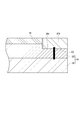
- FIG. 2 is a partially enlarged cross-sectional view of a support base and a focus ring of a plasma processing apparatus according to an exemplary embodiment.
- the support base 16 has a mounting area 20r.
- a focus ring FR is mounted on the mounting area 20r.
- the mounting region 20r is an outer peripheral region of the electrostatic chuck 20 in one example.
- the focus ring FR has a substantially annular plate shape.
- the focus ring FR has conductivity.
- the focus ring FR is made of, for example, silicon or silicon carbide (SiC).
- the substrate W has a disk shape and is disposed on the electrostatic chuck 20 and in a region surrounded by the focus ring FR. That is, the focus ring FR surrounds the edge of the substrate W placed on the support table 16.
- the plasma processing apparatus 1 further includes an upper electrode 30.
- the upper electrode 30 is provided above the support base 16.
- the upper electrode 30 closes the upper opening of the chamber body 12 together with the member 32.
- the member 32 has an insulating property.
- the upper electrode 30 is supported on the upper portion of the chamber body 12 through the member 32.
- the upper electrode 30 includes a top plate 34 and a support 36.
- the lower surface of the top plate 34 defines an internal space 10s.
- a plurality of gas discharge holes 34 a are formed in the top plate 34. Each of the plurality of gas discharge holes 34a penetrates the top plate 34 in the plate thickness direction (vertical direction).
- this top plate 34 is not limited, it is formed from silicon, for example.
- the top plate 34 may have a structure in which a plasma-resistant film is provided on the surface of an aluminum member. This film may be a ceramic film such as a film formed by anodization or a film formed from yttrium oxide.
- the support 36 detachably supports the top plate 34.
- the support 36 is made of a conductive material such as aluminum.
- a gas diffusion chamber 36 a is provided inside the support 36.
- a plurality of gas holes 36b extend downward from the gas diffusion chamber 36a.
- the plurality of gas holes 36b communicate with the plurality of gas discharge holes 34a, respectively.
- a gas introduction port 36 c is formed in the support 36.
- the gas introduction port 36c is connected to the gas diffusion chamber 36a.
- a gas supply pipe 38 is connected to the gas introduction port 36c.
- a gas source group 40 is connected to the gas supply pipe 38 via a valve group 41, a flow rate controller group 42, and a valve group 43.
- the gas source group 40, the valve group 41, the flow rate controller group 42, and the valve group 43 constitute a gas supply unit.
- the gas source group 40 includes a plurality of gas sources.
- Each of the valve group 41 and the valve group 43 includes a plurality of valves (for example, open / close valves).
- the flow rate controller group 42 includes a plurality of flow rate controllers.
- Each of the plurality of flow controllers in the flow controller group 42 is a mass flow controller or a pressure control type flow controller.
- Each of the plurality of gas sources of the gas source group 40 is connected to the gas supply pipe 38 via a corresponding valve of the valve group 41, a corresponding flow rate controller of the flow rate controller group 42, and a corresponding valve of the valve group 43. It is connected.
- the plasma processing apparatus 1 can supply the gas from one or more gas sources selected from the plurality of gas sources of the gas source group 40 to the internal space 10 s at individually adjusted flow rates.
- a baffle plate 48 is provided between the cylindrical portion 28 and the side wall of the chamber body 12.
- the baffle plate 48 can be configured by, for example, coating an aluminum member with a ceramic such as yttrium oxide.
- a number of through holes are formed in the baffle plate 48.
- An exhaust device 50 is connected to the exhaust pipe 52.
- the exhaust device 50 includes a pressure controller such as an automatic pressure control valve and a vacuum pump such as a turbo molecular pump, and can reduce the pressure in the internal space 10s.
- the plasma processing apparatus 1 may further include a high frequency power supply 61.
- the high frequency power supply 61 is a power supply that generates high frequency power HF for plasma generation.
- the high frequency power HF has a frequency within a range of 27 to 100 MHz, for example, a frequency of 40 MHz or 60 MHz.
- the high frequency power supply 61 is connected to the lower electrode 18 through the matching unit 63 and the electrode plate 21 in order to supply the high frequency power HF to the lower electrode 18.
- the matching unit 63 has a matching circuit for matching the output impedance of the high frequency power supply 61 with the impedance on the load side (lower electrode 18 side). Note that the high frequency power supply 61 may not be electrically connected to the lower electrode 18, and may be connected to the upper electrode 30 via the matching unit 63.
- the plasma processing apparatus 1 further includes a high frequency power supply 62.
- the high frequency power source 62 is a power source that generates bias high frequency power for drawing ions into the substrate W, that is, high frequency power LF.
- the frequency of the high frequency power LF is lower than the frequency of the high frequency power HF.
- the frequency of the high-frequency power LF is a frequency within a range of 400 kHz to 13.56 MHz, for example, 400 kHz.
- the high frequency power supply 62 is connected to the lower electrode 18 via the matching unit 64 and the electrode plate 21 in order to supply the high frequency power LF to the lower electrode 18.
- the matching unit 64 has a matching circuit for matching the output impedance of the high-frequency power source 62 with the impedance on the load side (lower electrode 18 side).
- gas is supplied to the internal space 10s. And by supplying the high frequency power HF and the high frequency power LF, or the high frequency power LF, the gas is excited in the internal space 10s. As a result, plasma is generated in the internal space 10s.
- the substrate W is processed by chemical species such as ions and / or radicals from the generated plasma.
- the plasma processing apparatus 1 may further include a measurement circuit 70.
- the measurement circuit 70 includes a voltage sensor 70v.
- the measurement circuit 70 is electrically connected to the lower electrode 18 via the power supply line of the high frequency power LF and the electrode plate 21.
- the lower electrode 18 is electrically connected to the focus ring FR via a conductor 22.
- the measurement circuit 70 may be electrically connected to the focus ring FR without passing through one or more of the power supply line of the high-frequency power LF, the electrode plate 21, and the lower electrode 18.
- the measurement circuit 70 may be connected to the focus ring FR via another electrical path.
- the measurement circuit 70 has a voltage sensor 70v.
- the measurement circuit 70 may further include a current sensor 70i.
- measurement circuit 70 includes a voltage divider circuit.
- the voltage divider circuit is a resistor voltage divider circuit.
- the voltage sensor 70v is connected to a node between two resistors of the resistance voltage dividing circuit.
- the voltage sensor 70v is configured to acquire a measured value of the voltage at the node, that is, a measured value representing a DC potential of the focus ring FR (hereinafter referred to as “potential measured value”).
- the potential measurement value acquired by the voltage sensor 70v is transmitted to the control unit MC described later.
- the measurement circuit 70 may further include a current sensor 70i.
- the current sensor 70 i is configured to acquire a measurement value (hereinafter referred to as “current measurement value”) of a current flowing through an electrical path connecting the focus ring FR and the measurement circuit 70.
- the current measurement value acquired by the current sensor 70i is transmitted to the control unit MC.
- the plasma processing apparatus 1 may further include a DC power source 72.
- the DC power source 72 is configured to apply a negative DC voltage to the focus ring FR.
- a negative DC voltage from the DC power source 72 to the focus ring FR.
- the thickness of the sheath (plasma sheath) above the focus ring FR is adjusted.
- the incident direction of ions with respect to the edge of the substrate W is adjusted.
- the measurement circuit 70 and the DC power source 72 are configured to be selectively connected to the focus ring FR.
- the plasma processing apparatus 1 includes one or more switching elements.
- the plasma processing apparatus 1 includes a switching element 70s and a switching element 72s in order to selectively connect one of the measurement circuit 70 and the DC power source 72 to the focus ring FR.
- Each of the switching element 70s and the switching element 72s may be a field effect transistor, for example.
- the switching element 70s becomes conductive
- the end of the voltage dividing circuit of the measurement circuit 70 opposite to the ground is connected to the focus ring FR.
- the switching element 72s becomes conductive, the DC power source 72 is connected to the focus ring FR.
- the switching element 70s and the switching element 72s are controlled by the control unit MC so that when one of the switching element 70s and the switching element 72s is in the conductive state, the other is in the non-passing state.
- the plasma processing apparatus 1 may further include a high frequency cutoff filter 74.
- the high frequency cutoff filter 74 is provided to prevent high frequency power from flowing into the measurement circuit 70 and the DC power source 72.
- the high frequency cutoff filter 74 has a capacitor, for example. One end of the capacitor of the high frequency cutoff filter 74 is connected to the electrical path between the focus ring FR and the voltage dividing circuit of the measurement circuit 70 and between the focus ring FR and the DC power source 72. The other end of the capacitor of the high frequency cutoff filter 74 is connected to the ground.
- the plasma processing apparatus 1 further includes a control unit MC.
- the control unit MC is a computer including a processor, a storage device, an input device, a display device, and the like, and controls each unit of the plasma processing apparatus 1.
- the control unit MC executes a control program stored in the storage device, and controls each unit of the plasma processing apparatus 1 based on recipe data stored in the storage device.
- the plasma processing apparatus 1 can execute the process specified by the recipe data.
- the plasma processing apparatus 1 can execute the methods according to various embodiments under the control of the control unit MC.
- FIG. 3 is a flow diagram illustrating a method for controlling a high frequency power source of a plasma processing apparatus according to one exemplary embodiment.
- step ST1 the control unit MC specifies the power level of the high-frequency power LF corresponding to the designated value of the DC potential of the focus ring FR using a table or a function.
- the specified value of the DC potential of the focus ring FR may be input to the control unit MC by an operator. Alternatively, the specified value of the DC potential of the focus ring FR may be stored in the storage device of the control unit MC as part of the recipe data.
- the table or function used by the controller MC defines the relationship between the power level of the high-frequency power LF and the DC potential of the focus ring FR generated by the supply of the high-frequency power LF to the lower electrode 18.
- the table or function is given to the control unit MC in advance. A method of creating a table or function that defines the relationship between the DC potential of the focus ring FR and the power level of the high-frequency power LF will be described later.
- the measurement circuit 70 is connected to the focus ring FR and the DC power source 72 is electrically disconnected from the focus ring FR during the execution of the steps ST2 and ST3.
- plasma is generated.
- the gas supply unit is controlled by the control unit MC so as to supply the gas into the chamber 10.
- the exhaust device 50 is controlled so as to set the pressure in the chamber 10 to a specified pressure.
- the high-frequency power source 62 is controlled by the control unit MC so that the high-frequency power LF having the power level specified in step ST1 is supplied to the lower electrode 18.
- the high frequency power supply 61 may be controlled by the control unit MC so as to supply the high frequency power HF to the lower electrode 18 (or the upper electrode 30).
- step ST3 is performed during plasma generation.
- plasma can be continuously generated from step ST2.
- step ST3 a potential measurement value representing the DC potential of the focus ring FR is acquired by the measurement circuit 70.
- the high frequency power supply 62 is controlled by the control unit MC so as to adjust the power level of the high frequency power LF in order to reduce the difference between the designated value and the DC potential of the focus ring FR determined from the measured potential value. Be controlled.
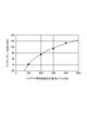
- FIG. 4 is a graph showing an example of the relationship between the power level of the bias high frequency power and the etching rate.
- the horizontal axis indicates the power level of the bias high-frequency power (high-frequency power LF), and the vertical axis indicates the etching rate.
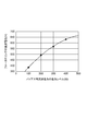
- FIG. 5 is a graph showing an example of the relationship between the DC potential of the focus ring and the etching rate.
- the horizontal axis indicates the DC potential of the focus ring FR
- the vertical axis indicates the etching rate.
- FIG. 6 is a graph showing an example of the relationship between the power level of the bias high-frequency power and the DC potential of the focus ring generated by supplying the bias high-frequency power to the lower electrode.
- plasma etching was performed on the silicon oxide film using the plasma processing apparatus 1 with the power level of the high-frequency power LF set to various values.
- the frequency of the high frequency power LF was 13 MHz.
- a fluorocarbon gas was supplied into the chamber 10 and the pressure in the chamber 10 was set to 20 mTorr (2.7 Pa).
- the frequency and power level of the high-frequency power HF were set to 40 MHz and 500 W, respectively.
- the relationship between the power level of the high frequency power LF and the etching rate of the silicon oxide film was obtained.
- FIG. 4 shows the relationship between the obtained power level of the high frequency power LF and the etching rate of the silicon oxide film.
- the DC potential of the focus ring FR was obtained using the voltage sensor 70v of the measurement circuit 70. Then, the relationship between the DC potential of the focus ring FR and the etching rate of the silicon oxide film was obtained. Further, the relationship between the power level of the high-frequency power LF and the DC potential of the focus ring FR was obtained.
- FIG. 5 shows the relationship between the obtained DC potential of the focus ring FR and the etching rate of the silicon oxide film.
- FIG. 6 shows the relationship between the obtained power level of the high frequency power LF and the DC potential of the focus ring FR.
- the etching rate increases with an increase in the bias high frequency power, that is, the power level of the high frequency power LF.
- the power level of the high-frequency power LF has a non-linear relationship with the etching rate.
- the direct current potential of the focus ring FR generated by supplying the high frequency power LF during the generation of plasma is substantially the same as the direct current potential of the substrate W.
- the power level of the high frequency power LF set at the time of plasma generation uses a table or function that represents the relationship between the DC potential of the focus ring FR and the power level of the high frequency power LF as shown in FIG. Determined.
- the power level of the high-frequency power LF that is set when plasma is generated is determined based on the DC potential of the focus ring FR that has a substantially linear proportional relationship with the etching rate. Therefore, according to the plasma processing apparatus 1, the controllability of the etching rate is improved.
- the DC potential of the focus ring FR may change due to, for example, a change in the state of the plasma processing apparatus 1.
- the power level of the high-frequency power LF is adjusted so as to reduce the difference between the actual focus ring FR DC potential obtained from the measured potential of the measurement circuit 70 and the specified value. The Therefore, a desired etching rate is realized with high accuracy.
- the DC power source 72 can be selectively connected to the focus ring FR. According to this embodiment, it is possible to apply a DC voltage to the focus ring FR. Further, when measuring the measured value of the DC potential of the focus ring FR, the DC power source 72 can be electrically disconnected from the focus ring FR.
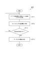
- FIG. 7 is a flow diagram illustrating a method of creating a table or function that defines the relationship between the DC potential of the focus ring and the power level of the bias high frequency power, according to one exemplary embodiment.
- step ST11 The creation method shown in FIG. 7 (hereinafter referred to as “method MTF”) starts in step ST11.
- plasma is generated in the chamber 10.
- conditions such as the gas supplied into the chamber 10, the pressure in the chamber 10, and the power level of the high frequency power HF are the same as those in the process ST2 and the process ST3 of the method MT.
- the power level of the high-frequency power LF is set to one power level that is sequentially selected from a plurality of power levels.
- step ST12 the DC potential of the focus ring FR is specified from the potential measurement value of the measurement circuit 70.
- step ST12 one data set including the DC potential of the identified focus ring FR and the power level of the high-frequency power LF set in step ST11 is acquired.
- step ST13 it is determined whether or not the stop condition is satisfied.
- the stop condition is satisfied when the process ST11 has already been executed for all of the plurality of power levels described above. If it is determined in step ST13 that the stop condition is not satisfied, steps ST11 and ST12 are executed again.
- step ST11 the power level of the high-frequency power LF is set to one unselected power level among the plurality of power levels.
- step ST14 the process proceeds to step ST14.
- step ST14 a table or function representing the relationship between the DC potential of the focus ring FR and the power level of the high frequency power LF is created using a plurality of data sets obtained by repeating the sequence including the steps ST11 and ST12.
- the table or function created by the method MTF is used by the control unit MC to determine the power level of the high-frequency power LF from the specified value.
- the plasma processing apparatus may be any type of plasma processing apparatus different from the capacitively coupled plasma processing apparatus.
- a plasma processing apparatus include an inductively coupled plasma processing apparatus and a plasma processing apparatus that generates plasma using surface waves such as microwaves.
Landscapes
- Engineering & Computer Science (AREA)
- Physics & Mathematics (AREA)
- Plasma & Fusion (AREA)
- Analytical Chemistry (AREA)
- Chemical & Material Sciences (AREA)
- Manufacturing & Machinery (AREA)
- Microelectronics & Electronic Packaging (AREA)
- Power Engineering (AREA)
- Computer Hardware Design (AREA)
- General Physics & Mathematics (AREA)
- Condensed Matter Physics & Semiconductors (AREA)
- Electromagnetism (AREA)
- Spectroscopy & Molecular Physics (AREA)
- Drying Of Semiconductors (AREA)
- Plasma Technology (AREA)
- Container, Conveyance, Adherence, Positioning, Of Wafer (AREA)
- Chemical Vapour Deposition (AREA)
Priority Applications (3)
| Application Number | Priority Date | Filing Date | Title |
|---|---|---|---|
| CN201980004435.4A CN111095497B (zh) | 2018-06-12 | 2019-06-03 | 等离子体处理装置以及控制其高频电源的方法 |
| KR1020207007023A KR102812745B1 (ko) | 2018-06-12 | 2019-06-03 | 플라즈마 처리 장치 및 플라즈마 처리 장치의 고주파 전원을 제어하는 방법 |
| US16/645,695 US11264208B2 (en) | 2018-06-12 | 2019-06-03 | Plasma processing apparatus and method for controlling radio-frequency power supply of plasma processing apparatus |
Applications Claiming Priority (2)
| Application Number | Priority Date | Filing Date | Title |
|---|---|---|---|
| JP2018-111973 | 2018-06-12 | ||
| JP2018111973A JP6846384B2 (ja) | 2018-06-12 | 2018-06-12 | プラズマ処理装置及びプラズマ処理装置の高周波電源を制御する方法 |
Publications (1)
| Publication Number | Publication Date |
|---|---|
| WO2019239944A1 true WO2019239944A1 (ja) | 2019-12-19 |
Family
ID=68842142
Family Applications (1)
| Application Number | Title | Priority Date | Filing Date |
|---|---|---|---|
| PCT/JP2019/022024 Ceased WO2019239944A1 (ja) | 2018-06-12 | 2019-06-03 | プラズマ処理装置及びプラズマ処理装置の高周波電源を制御する方法 |
Country Status (6)
| Country | Link |
|---|---|
| US (1) | US11264208B2 (enExample) |
| JP (1) | JP6846384B2 (enExample) |
| KR (1) | KR102812745B1 (enExample) |
| CN (1) | CN111095497B (enExample) |
| TW (1) | TWI814837B (enExample) |
| WO (1) | WO2019239944A1 (enExample) |
Cited By (1)
| Publication number | Priority date | Publication date | Assignee | Title |
|---|---|---|---|---|
| JP2022065968A (ja) * | 2020-10-16 | 2022-04-28 | 東京エレクトロン株式会社 | 基板処理システム、制御方法及び制御プログラム |
Families Citing this family (27)
| Publication number | Priority date | Publication date | Assignee | Title |
|---|---|---|---|---|
| US10510575B2 (en) | 2017-09-20 | 2019-12-17 | Applied Materials, Inc. | Substrate support with multiple embedded electrodes |
| US10555412B2 (en) | 2018-05-10 | 2020-02-04 | Applied Materials, Inc. | Method of controlling ion energy distribution using a pulse generator with a current-return output stage |
| US11476145B2 (en) | 2018-11-20 | 2022-10-18 | Applied Materials, Inc. | Automatic ESC bias compensation when using pulsed DC bias |
| JP7451540B2 (ja) | 2019-01-22 | 2024-03-18 | アプライド マテリアルズ インコーポレイテッド | パルス状電圧波形を制御するためのフィードバックループ |
| US11508554B2 (en) | 2019-01-24 | 2022-11-22 | Applied Materials, Inc. | High voltage filter assembly |
| JP7504686B2 (ja) * | 2020-07-15 | 2024-06-24 | 東京エレクトロン株式会社 | プラズマ処理装置及びプラズマ処理方法 |
| US11462389B2 (en) | 2020-07-31 | 2022-10-04 | Applied Materials, Inc. | Pulsed-voltage hardware assembly for use in a plasma processing system |
| CN112538619A (zh) * | 2020-11-05 | 2021-03-23 | 宣城睿晖宣晟企业管理中心合伙企业(有限合伙) | 一种射频电源的控制方法及装置 |
| US11901157B2 (en) | 2020-11-16 | 2024-02-13 | Applied Materials, Inc. | Apparatus and methods for controlling ion energy distribution |
| US11798790B2 (en) | 2020-11-16 | 2023-10-24 | Applied Materials, Inc. | Apparatus and methods for controlling ion energy distribution |
| US11495470B1 (en) | 2021-04-16 | 2022-11-08 | Applied Materials, Inc. | Method of enhancing etching selectivity using a pulsed plasma |
| US11791138B2 (en) | 2021-05-12 | 2023-10-17 | Applied Materials, Inc. | Automatic electrostatic chuck bias compensation during plasma processing |
| US11948780B2 (en) | 2021-05-12 | 2024-04-02 | Applied Materials, Inc. | Automatic electrostatic chuck bias compensation during plasma processing |
| US11967483B2 (en) | 2021-06-02 | 2024-04-23 | Applied Materials, Inc. | Plasma excitation with ion energy control |
| US20220399185A1 (en) | 2021-06-09 | 2022-12-15 | Applied Materials, Inc. | Plasma chamber and chamber component cleaning methods |
| US12148595B2 (en) | 2021-06-09 | 2024-11-19 | Applied Materials, Inc. | Plasma uniformity control in pulsed DC plasma chamber |
| US11810760B2 (en) | 2021-06-16 | 2023-11-07 | Applied Materials, Inc. | Apparatus and method of ion current compensation |
| US11569066B2 (en) | 2021-06-23 | 2023-01-31 | Applied Materials, Inc. | Pulsed voltage source for plasma processing applications |
| US11776788B2 (en) | 2021-06-28 | 2023-10-03 | Applied Materials, Inc. | Pulsed voltage boost for substrate processing |
| US11476090B1 (en) | 2021-08-24 | 2022-10-18 | Applied Materials, Inc. | Voltage pulse time-domain multiplexing |
| US12106938B2 (en) | 2021-09-14 | 2024-10-01 | Applied Materials, Inc. | Distortion current mitigation in a radio frequency plasma processing chamber |
| US11694876B2 (en) | 2021-12-08 | 2023-07-04 | Applied Materials, Inc. | Apparatus and method for delivering a plurality of waveform signals during plasma processing |
| US11972924B2 (en) | 2022-06-08 | 2024-04-30 | Applied Materials, Inc. | Pulsed voltage source for plasma processing applications |
| US12315732B2 (en) | 2022-06-10 | 2025-05-27 | Applied Materials, Inc. | Method and apparatus for etching a semiconductor substrate in a plasma etch chamber |
| US12272524B2 (en) | 2022-09-19 | 2025-04-08 | Applied Materials, Inc. | Wideband variable impedance load for high volume manufacturing qualification and on-site diagnostics |
| JPWO2024070268A1 (enExample) * | 2022-09-29 | 2024-04-04 | ||
| US12111341B2 (en) | 2022-10-05 | 2024-10-08 | Applied Materials, Inc. | In-situ electric field detection method and apparatus |
Citations (6)
| Publication number | Priority date | Publication date | Assignee | Title |
|---|---|---|---|---|
| JP2007258417A (ja) * | 2006-03-23 | 2007-10-04 | Tokyo Electron Ltd | プラズマ処理方法 |
| JP2008227063A (ja) * | 2007-03-12 | 2008-09-25 | Tokyo Electron Ltd | プラズマ処理装置及びプラズマ分布補正方法 |
| JP2010524157A (ja) * | 2007-03-30 | 2010-07-15 | ラム リサーチ コーポレーション | Rf作動電極のdc電圧制御方法及び装置 |
| JP2010186841A (ja) * | 2009-02-12 | 2010-08-26 | Hitachi High-Technologies Corp | プラズマ処理方法 |
| JP2010283028A (ja) * | 2009-06-02 | 2010-12-16 | Tokyo Electron Ltd | プラズマ処理装置,プラズマ処理方法,プログラム |
| JP2017228558A (ja) * | 2016-06-20 | 2017-12-28 | 東京エレクトロン株式会社 | プラズマ処理装置、及び波形補正方法 |
Family Cites Families (16)
| Publication number | Priority date | Publication date | Assignee | Title |
|---|---|---|---|---|
| JP3173693B2 (ja) * | 1993-10-04 | 2001-06-04 | 東京エレクトロン株式会社 | プラズマ処理装置及びその方法 |
| JP4219628B2 (ja) | 2001-07-27 | 2009-02-04 | 東京エレクトロン株式会社 | プラズマ処理装置および基板載置台 |
| TW200520632A (en) * | 2003-09-05 | 2005-06-16 | Tokyo Electron Ltd | Focus ring and plasma processing apparatus |
| JP4421874B2 (ja) * | 2003-10-31 | 2010-02-24 | 東京エレクトロン株式会社 | プラズマ処理装置及びプラズマ処理方法 |
| JP4672456B2 (ja) * | 2004-06-21 | 2011-04-20 | 東京エレクトロン株式会社 | プラズマ処理装置 |
| JP4597894B2 (ja) * | 2006-03-31 | 2010-12-15 | 東京エレクトロン株式会社 | 基板載置台および基板処理装置 |
| US8563619B2 (en) * | 2007-06-28 | 2013-10-22 | Lam Research Corporation | Methods and arrangements for plasma processing system with tunable capacitance |
| JP5657262B2 (ja) * | 2009-03-27 | 2015-01-21 | 東京エレクトロン株式会社 | プラズマ処理装置 |
| JP5563347B2 (ja) * | 2010-03-30 | 2014-07-30 | 東京エレクトロン株式会社 | プラズマ処理装置及び半導体装置の製造方法 |
| JP5864879B2 (ja) * | 2011-03-31 | 2016-02-17 | 東京エレクトロン株式会社 | 基板処理装置及びその制御方法 |
| JP6224958B2 (ja) * | 2013-02-20 | 2017-11-01 | 東京エレクトロン株式会社 | プラズマ処理装置及びプラズマ処理方法 |
| JP6573325B2 (ja) * | 2013-12-17 | 2019-09-11 | 東京エレクトロン株式会社 | プラズマ密度を制御するシステムおよび方法 |
| JP6244518B2 (ja) * | 2014-04-09 | 2017-12-13 | 東京エレクトロン株式会社 | プラズマ処理方法及びプラズマ処理装置 |
| JP2016031955A (ja) * | 2014-07-28 | 2016-03-07 | 株式会社日立ハイテクノロジーズ | プラズマ処理装置およびプラズマ処理方法 |
| JP2017028111A (ja) * | 2015-07-23 | 2017-02-02 | 株式会社日立ハイテクノロジーズ | プラズマ処理装置 |
| JP6826955B2 (ja) * | 2017-06-14 | 2021-02-10 | 東京エレクトロン株式会社 | プラズマ処理装置及びプラズマ処理方法 |
-
2018
- 2018-06-12 JP JP2018111973A patent/JP6846384B2/ja active Active
-
2019
- 2019-06-03 WO PCT/JP2019/022024 patent/WO2019239944A1/ja not_active Ceased
- 2019-06-03 US US16/645,695 patent/US11264208B2/en active Active
- 2019-06-03 KR KR1020207007023A patent/KR102812745B1/ko active Active
- 2019-06-03 CN CN201980004435.4A patent/CN111095497B/zh active Active
- 2019-06-06 TW TW108119645A patent/TWI814837B/zh active
Patent Citations (6)
| Publication number | Priority date | Publication date | Assignee | Title |
|---|---|---|---|---|
| JP2007258417A (ja) * | 2006-03-23 | 2007-10-04 | Tokyo Electron Ltd | プラズマ処理方法 |
| JP2008227063A (ja) * | 2007-03-12 | 2008-09-25 | Tokyo Electron Ltd | プラズマ処理装置及びプラズマ分布補正方法 |
| JP2010524157A (ja) * | 2007-03-30 | 2010-07-15 | ラム リサーチ コーポレーション | Rf作動電極のdc電圧制御方法及び装置 |
| JP2010186841A (ja) * | 2009-02-12 | 2010-08-26 | Hitachi High-Technologies Corp | プラズマ処理方法 |
| JP2010283028A (ja) * | 2009-06-02 | 2010-12-16 | Tokyo Electron Ltd | プラズマ処理装置,プラズマ処理方法,プログラム |
| JP2017228558A (ja) * | 2016-06-20 | 2017-12-28 | 東京エレクトロン株式会社 | プラズマ処理装置、及び波形補正方法 |
Cited By (2)
| Publication number | Priority date | Publication date | Assignee | Title |
|---|---|---|---|---|
| JP2022065968A (ja) * | 2020-10-16 | 2022-04-28 | 東京エレクトロン株式会社 | 基板処理システム、制御方法及び制御プログラム |
| JP7505959B2 (ja) | 2020-10-16 | 2024-06-25 | 東京エレクトロン株式会社 | 基板処理システム、制御方法及び制御プログラム |
Also Published As
| Publication number | Publication date |
|---|---|
| US11264208B2 (en) | 2022-03-01 |
| KR20210019399A (ko) | 2021-02-22 |
| CN111095497A (zh) | 2020-05-01 |
| US20200266035A1 (en) | 2020-08-20 |
| KR102812745B1 (ko) | 2025-05-23 |
| TW202013425A (zh) | 2020-04-01 |
| TWI814837B (zh) | 2023-09-11 |
| JP2019216164A (ja) | 2019-12-19 |
| JP6846384B2 (ja) | 2021-03-24 |
| CN111095497B (zh) | 2024-05-07 |
Similar Documents
| Publication | Publication Date | Title |
|---|---|---|
| JP6846384B2 (ja) | プラズマ処理装置及びプラズマ処理装置の高周波電源を制御する方法 | |
| US11404281B2 (en) | Method of etching silicon containing films selectively against each other | |
| KR102820388B1 (ko) | 제어 방법 및 플라즈마 처리 장치 | |
| US20210074522A1 (en) | Plasma processing apparatus, electrostatic attraction method, and electrostatic attraction program | |
| US11171007B2 (en) | Plasma processing apparatus and plasma etching method | |
| US9991100B2 (en) | Plasma processing apparatus and control method | |
| US20200185193A1 (en) | Plasma processing apparatus and etching method | |
| US11342165B2 (en) | Plasma processing method | |
| CN111029237B (zh) | 基板支承组件、等离子体处理装置、以及等离子体处理方法 | |
| US20190237305A1 (en) | Method for applying dc voltage and plasma processing apparatus | |
| US12125672B2 (en) | Plasma processing method and plasma processing apparatus | |
| JP2021090018A (ja) | エッジリング及び基板処理装置 | |
| US20210296091A1 (en) | Inspection method, inspection apparatus, and plasma processing apparatus | |
| JP2022143200A (ja) | プラズマ処理装置、及びプラズマ処理装置を制御する方法 |
Legal Events
| Date | Code | Title | Description |
|---|---|---|---|
| 121 | Ep: the epo has been informed by wipo that ep was designated in this application |
Ref document number: 19820187 Country of ref document: EP Kind code of ref document: A1 |
|
| NENP | Non-entry into the national phase |
Ref country code: DE |
|
| 122 | Ep: pct application non-entry in european phase |
Ref document number: 19820187 Country of ref document: EP Kind code of ref document: A1 |