JP6846384B2 - プラズマ処理装置及びプラズマ処理装置の高周波電源を制御する方法 - Google Patents
プラズマ処理装置及びプラズマ処理装置の高周波電源を制御する方法 Download PDFInfo
- Publication number
- JP6846384B2 JP6846384B2 JP2018111973A JP2018111973A JP6846384B2 JP 6846384 B2 JP6846384 B2 JP 6846384B2 JP 2018111973 A JP2018111973 A JP 2018111973A JP 2018111973 A JP2018111973 A JP 2018111973A JP 6846384 B2 JP6846384 B2 JP 6846384B2
- Authority
- JP
- Japan
- Prior art keywords
- frequency power
- high frequency
- focus ring
- plasma processing
- potential
- Prior art date
- Legal status (The legal status is an assumption and is not a legal conclusion. Google has not performed a legal analysis and makes no representation as to the accuracy of the status listed.)
- Active
Links
- 238000012545 processing Methods 0.000 title claims description 69
- 238000000034 method Methods 0.000 title claims description 23
- 239000000758 substrate Substances 0.000 claims description 29
- 238000005259 measurement Methods 0.000 claims description 17
- 238000005530 etching Methods 0.000 description 25
- 238000001020 plasma etching Methods 0.000 description 8
- VYPSYNLAJGMNEJ-UHFFFAOYSA-N silicon dioxide Inorganic materials O=[Si]=O VYPSYNLAJGMNEJ-UHFFFAOYSA-N 0.000 description 7
- XAGFODPZIPBFFR-UHFFFAOYSA-N aluminium Chemical compound [Al] XAGFODPZIPBFFR-UHFFFAOYSA-N 0.000 description 6
- 229910052782 aluminium Inorganic materials 0.000 description 6
- 239000004020 conductor Substances 0.000 description 5
- 229910052814 silicon oxide Inorganic materials 0.000 description 5
- 239000000919 ceramic Substances 0.000 description 4
- 150000002500 ions Chemical class 0.000 description 4
- 239000003990 capacitor Substances 0.000 description 3
- 238000009792 diffusion process Methods 0.000 description 3
- 238000004519 manufacturing process Methods 0.000 description 3
- SIWVEOZUMHYXCS-UHFFFAOYSA-N oxo(oxoyttriooxy)yttrium Chemical compound O=[Y]O[Y]=O SIWVEOZUMHYXCS-UHFFFAOYSA-N 0.000 description 3
- 101001139126 Homo sapiens Krueppel-like factor 6 Proteins 0.000 description 2
- 238000007743 anodising Methods 0.000 description 2
- 239000010453 quartz Substances 0.000 description 2
- 239000003507 refrigerant Substances 0.000 description 2
- 229910052710 silicon Inorganic materials 0.000 description 2
- 239000010703 silicon Substances 0.000 description 2
- 230000000903 blocking effect Effects 0.000 description 1
- 239000013626 chemical specie Substances 0.000 description 1
- KYKAJFCTULSVSH-UHFFFAOYSA-N chloro(fluoro)methane Chemical compound F[C]Cl KYKAJFCTULSVSH-UHFFFAOYSA-N 0.000 description 1
- 239000011248 coating agent Substances 0.000 description 1
- 238000000576 coating method Methods 0.000 description 1
- 238000010586 diagram Methods 0.000 description 1
- 239000003989 dielectric material Substances 0.000 description 1
- 230000005669 field effect Effects 0.000 description 1
- NBVXSUQYWXRMNV-UHFFFAOYSA-N fluoromethane Chemical compound FC NBVXSUQYWXRMNV-UHFFFAOYSA-N 0.000 description 1
- 238000009616 inductively coupled plasma Methods 0.000 description 1
- 239000011810 insulating material Substances 0.000 description 1
- 239000007788 liquid Substances 0.000 description 1
- 239000000463 material Substances 0.000 description 1
- 238000012986 modification Methods 0.000 description 1
- 230000004048 modification Effects 0.000 description 1
- 230000002093 peripheral effect Effects 0.000 description 1
- HBMJWWWQQXIZIP-UHFFFAOYSA-N silicon carbide Chemical compound [Si+]#[C-] HBMJWWWQQXIZIP-UHFFFAOYSA-N 0.000 description 1
- 238000006467 substitution reaction Methods 0.000 description 1
- 238000012546 transfer Methods 0.000 description 1
- 238000009834 vaporization Methods 0.000 description 1
- 230000008016 vaporization Effects 0.000 description 1
Images


Classifications
-
- H—ELECTRICITY
- H01—ELECTRIC ELEMENTS
- H01J—ELECTRIC DISCHARGE TUBES OR DISCHARGE LAMPS
- H01J37/00—Discharge tubes with provision for introducing objects or material to be exposed to the discharge, e.g. for the purpose of examination or processing thereof
- H01J37/32—Gas-filled discharge tubes
- H01J37/32431—Constructional details of the reactor
- H01J37/32733—Means for moving the material to be treated
- H01J37/32743—Means for moving the material to be treated for introducing the material into processing chamber
-
- H—ELECTRICITY
- H01—ELECTRIC ELEMENTS
- H01J—ELECTRIC DISCHARGE TUBES OR DISCHARGE LAMPS
- H01J37/00—Discharge tubes with provision for introducing objects or material to be exposed to the discharge, e.g. for the purpose of examination or processing thereof
- H01J37/32—Gas-filled discharge tubes
- H01J37/32009—Arrangements for generation of plasma specially adapted for examination or treatment of objects, e.g. plasma sources
- H01J37/32082—Radio frequency generated discharge
- H01J37/32174—Circuits specially adapted for controlling the RF discharge
-
- H—ELECTRICITY
- H01—ELECTRIC ELEMENTS
- H01J—ELECTRIC DISCHARGE TUBES OR DISCHARGE LAMPS
- H01J37/00—Discharge tubes with provision for introducing objects or material to be exposed to the discharge, e.g. for the purpose of examination or processing thereof
- H01J37/32—Gas-filled discharge tubes
- H01J37/32009—Arrangements for generation of plasma specially adapted for examination or treatment of objects, e.g. plasma sources
- H01J37/32082—Radio frequency generated discharge
- H01J37/32091—Radio frequency generated discharge the radio frequency energy being capacitively coupled to the plasma
-
- H—ELECTRICITY
- H01—ELECTRIC ELEMENTS
- H01J—ELECTRIC DISCHARGE TUBES OR DISCHARGE LAMPS
- H01J37/00—Discharge tubes with provision for introducing objects or material to be exposed to the discharge, e.g. for the purpose of examination or processing thereof
- H01J37/32—Gas-filled discharge tubes
- H01J37/32431—Constructional details of the reactor
- H01J37/32532—Electrodes
-
- H—ELECTRICITY
- H01—ELECTRIC ELEMENTS
- H01J—ELECTRIC DISCHARGE TUBES OR DISCHARGE LAMPS
- H01J37/00—Discharge tubes with provision for introducing objects or material to be exposed to the discharge, e.g. for the purpose of examination or processing thereof
- H01J37/32—Gas-filled discharge tubes
- H01J37/32431—Constructional details of the reactor
- H01J37/32623—Mechanical discharge control means
- H01J37/32642—Focus rings
-
- H—ELECTRICITY
- H01—ELECTRIC ELEMENTS
- H01J—ELECTRIC DISCHARGE TUBES OR DISCHARGE LAMPS
- H01J37/00—Discharge tubes with provision for introducing objects or material to be exposed to the discharge, e.g. for the purpose of examination or processing thereof
- H01J37/32—Gas-filled discharge tubes
- H01J37/32431—Constructional details of the reactor
- H01J37/32715—Workpiece holder
-
- H—ELECTRICITY
- H01—ELECTRIC ELEMENTS
- H01L—SEMICONDUCTOR DEVICES NOT COVERED BY CLASS H10
- H01L21/00—Processes or apparatus adapted for the manufacture or treatment of semiconductor or solid state devices or of parts thereof
- H01L21/02—Manufacture or treatment of semiconductor devices or of parts thereof
- H01L21/04—Manufacture or treatment of semiconductor devices or of parts thereof the devices having at least one potential-jump barrier or surface barrier, e.g. PN junction, depletion layer or carrier concentration layer
- H01L21/18—Manufacture or treatment of semiconductor devices or of parts thereof the devices having at least one potential-jump barrier or surface barrier, e.g. PN junction, depletion layer or carrier concentration layer the devices having semiconductor bodies comprising elements of Group IV of the Periodic System or AIIIBV compounds with or without impurities, e.g. doping materials
- H01L21/30—Treatment of semiconductor bodies using processes or apparatus not provided for in groups H01L21/20 - H01L21/26
- H01L21/302—Treatment of semiconductor bodies using processes or apparatus not provided for in groups H01L21/20 - H01L21/26 to change their surface-physical characteristics or shape, e.g. etching, polishing, cutting
- H01L21/306—Chemical or electrical treatment, e.g. electrolytic etching
- H01L21/3065—Plasma etching; Reactive-ion etching
-
- H—ELECTRICITY
- H01—ELECTRIC ELEMENTS
- H01L—SEMICONDUCTOR DEVICES NOT COVERED BY CLASS H10
- H01L21/00—Processes or apparatus adapted for the manufacture or treatment of semiconductor or solid state devices or of parts thereof
- H01L21/67—Apparatus specially adapted for handling semiconductor or electric solid state devices during manufacture or treatment thereof; Apparatus specially adapted for handling wafers during manufacture or treatment of semiconductor or electric solid state devices or components ; Apparatus not specifically provided for elsewhere
- H01L21/67005—Apparatus not specifically provided for elsewhere
- H01L21/67011—Apparatus for manufacture or treatment
- H01L21/67017—Apparatus for fluid treatment
- H01L21/67063—Apparatus for fluid treatment for etching
- H01L21/67069—Apparatus for fluid treatment for etching for drying etching
-
- H—ELECTRICITY
- H01—ELECTRIC ELEMENTS
- H01L—SEMICONDUCTOR DEVICES NOT COVERED BY CLASS H10
- H01L21/00—Processes or apparatus adapted for the manufacture or treatment of semiconductor or solid state devices or of parts thereof
- H01L21/67—Apparatus specially adapted for handling semiconductor or electric solid state devices during manufacture or treatment thereof; Apparatus specially adapted for handling wafers during manufacture or treatment of semiconductor or electric solid state devices or components ; Apparatus not specifically provided for elsewhere
- H01L21/683—Apparatus specially adapted for handling semiconductor or electric solid state devices during manufacture or treatment thereof; Apparatus specially adapted for handling wafers during manufacture or treatment of semiconductor or electric solid state devices or components ; Apparatus not specifically provided for elsewhere for supporting or gripping
- H01L21/6831—Apparatus specially adapted for handling semiconductor or electric solid state devices during manufacture or treatment thereof; Apparatus specially adapted for handling wafers during manufacture or treatment of semiconductor or electric solid state devices or components ; Apparatus not specifically provided for elsewhere for supporting or gripping using electrostatic chucks
- H01L21/6833—Details of electrostatic chucks
-
- H—ELECTRICITY
- H05—ELECTRIC TECHNIQUES NOT OTHERWISE PROVIDED FOR
- H05H—PLASMA TECHNIQUE; PRODUCTION OF ACCELERATED ELECTRICALLY-CHARGED PARTICLES OR OF NEUTRONS; PRODUCTION OR ACCELERATION OF NEUTRAL MOLECULAR OR ATOMIC BEAMS
- H05H1/00—Generating plasma; Handling plasma
- H05H1/24—Generating plasma
- H05H1/46—Generating plasma using applied electromagnetic fields, e.g. high frequency or microwave energy
-
- H—ELECTRICITY
- H01—ELECTRIC ELEMENTS
- H01J—ELECTRIC DISCHARGE TUBES OR DISCHARGE LAMPS
- H01J2237/00—Discharge tubes exposing object to beam, e.g. for analysis treatment, etching, imaging
- H01J2237/32—Processing objects by plasma generation
- H01J2237/33—Processing objects by plasma generation characterised by the type of processing
- H01J2237/334—Etching
Description
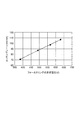
図5は、フォーカスリングの直流電位とエッチングレートとの関係の一例を示すグラフである。図5において、横軸は、フォーカスリングFRの直流電位を示しており、縦軸はエッチングレートを示している。図6は、バイアス高周波電力の電力レベルと下部電極へのバイアス高周波電力の供給により生じるフォーカスリングの直流電位との関係の一例を示すグラフである。
Claims (6)
- チャンバと、
下部電極を含み、前記チャンバ内に設けられた基板支持台と、
前記下部電極にバイアス高周波電力を供給するように構成された高周波電源と、
前記高周波電源を制御するように構成された制御部と、
を備え、
前記基板支持台上には、フォーカスリングが基板を囲むように搭載され、
前記制御部は、
前記バイアス高周波電力の電力レベルと前記下部電極への該バイアス高周波電力の供給により生じる前記フォーカスリングの直流電位との関係を規定するテーブル又は関数を用いて、前記フォーカスリングの直流電位の指定値に対応する前記バイアス高周波電力の電力レベルを特定し、
前記チャンバ内でのプラズマの生成中に、特定された前記電力レベルを有する前記バイアス高周波電力を前記下部電極に供給するように前記高周波電源を制御する、
プラズマ処理装置。 - 前記フォーカスリングの直流電位を表す測定値を取得するよう構成された測定回路を更に備え、
前記制御部は、前記チャンバ内でのプラズマの生成中に、前記指定値と前記測定値から決定される前記フォーカスリングの直流電位との間の差を減少させるよう前記バイアス高周波電力の電力レベルを調整する、
請求項1に記載のプラズマ処理装置。 - 前記フォーカスリングに選択的に接続されるように構成された直流電源を更に備える、請求項1又は2に記載のプラズマ処理装置。
- 前記プラズマ処理装置は、容量結合型のプラズマ処理装置である、請求項1〜3の何れか一項に記載のプラズマ処理装置。
- プラズマ処理装置の高周波電源を制御する方法であって、
バイアス高周波電力の電力レベルと基板支持台の下部電極への該バイアス高周波電力の供給により生じるフォーカスリングの直流電位との関係を規定するテーブル又は関数を用いて、前記フォーカスリングの直流電位の指定値に対応するバイアス高周波電力の電力レベルを特定する工程であり、前記基板支持台は前記プラズマ処理装置のチャンバ内に設けられており、前記フォーカスリングは該基板支持台上で基板を囲むように搭載される、該工程と、
前記チャンバ内でのプラズマの生成中に、特定された前記電力レベルを有するバイアス高周波電力を前記下部電極に供給するように前記高周波電源を制御する工程と、
を含む方法。 - 前記チャンバ内でのプラズマの生成中に、前記指定値と前記フォーカスリングの直流電位を表す測定値から決定される該フォーカスリングの該直流電位との間の差を減少させるよう、前記バイアス高周波電力の電力レベルを調整する工程を更に含む、請求項5に記載の方法。
Priority Applications (6)
| Application Number | Priority Date | Filing Date | Title |
|---|---|---|---|
| JP2018111973A JP6846384B2 (ja) | 2018-06-12 | 2018-06-12 | プラズマ処理装置及びプラズマ処理装置の高周波電源を制御する方法 |
| US16/645,695 US11264208B2 (en) | 2018-06-12 | 2019-06-03 | Plasma processing apparatus and method for controlling radio-frequency power supply of plasma processing apparatus |
| KR1020207007023A KR20210019399A (ko) | 2018-06-12 | 2019-06-03 | 플라즈마 처리 장치 및 플라즈마 처리 장치의 고주파 전원을 제어하는 방법 |
| CN201980004435.4A CN111095497A (zh) | 2018-06-12 | 2019-06-03 | 等离子体处理装置以及控制其高频电源的方法 |
| PCT/JP2019/022024 WO2019239944A1 (ja) | 2018-06-12 | 2019-06-03 | プラズマ処理装置及びプラズマ処理装置の高周波電源を制御する方法 |
| TW108119645A TWI814837B (zh) | 2018-06-12 | 2019-06-06 | 電漿處理裝置及電漿處理裝置的射頻電源之控制方法 |
Applications Claiming Priority (1)
| Application Number | Priority Date | Filing Date | Title |
|---|---|---|---|
| JP2018111973A JP6846384B2 (ja) | 2018-06-12 | 2018-06-12 | プラズマ処理装置及びプラズマ処理装置の高周波電源を制御する方法 |
Publications (3)
| Publication Number | Publication Date |
|---|---|
| JP2019216164A JP2019216164A (ja) | 2019-12-19 |
| JP2019216164A5 JP2019216164A5 (ja) | 2021-02-04 |
| JP6846384B2 true JP6846384B2 (ja) | 2021-03-24 |
Family
ID=68842142
Family Applications (1)
| Application Number | Title | Priority Date | Filing Date |
|---|---|---|---|
| JP2018111973A Active JP6846384B2 (ja) | 2018-06-12 | 2018-06-12 | プラズマ処理装置及びプラズマ処理装置の高周波電源を制御する方法 |
Country Status (6)
| Country | Link |
|---|---|
| US (1) | US11264208B2 (ja) |
| JP (1) | JP6846384B2 (ja) |
| KR (1) | KR20210019399A (ja) |
| CN (1) | CN111095497A (ja) |
| TW (1) | TWI814837B (ja) |
| WO (1) | WO2019239944A1 (ja) |
Families Citing this family (16)
| Publication number | Priority date | Publication date | Assignee | Title |
|---|---|---|---|---|
| US10555412B2 (en) | 2018-05-10 | 2020-02-04 | Applied Materials, Inc. | Method of controlling ion energy distribution using a pulse generator with a current-return output stage |
| US11476145B2 (en) | 2018-11-20 | 2022-10-18 | Applied Materials, Inc. | Automatic ESC bias compensation when using pulsed DC bias |
| JP7451540B2 (ja) | 2019-01-22 | 2024-03-18 | アプライド マテリアルズ インコーポレイテッド | パルス状電圧波形を制御するためのフィードバックループ |
| US11508554B2 (en) | 2019-01-24 | 2022-11-22 | Applied Materials, Inc. | High voltage filter assembly |
| US11462389B2 (en) | 2020-07-31 | 2022-10-04 | Applied Materials, Inc. | Pulsed-voltage hardware assembly for use in a plasma processing system |
| JP2022065968A (ja) | 2020-10-16 | 2022-04-28 | 東京エレクトロン株式会社 | 基板処理システム、制御方法及び制御プログラム |
| CN112538619A (zh) * | 2020-11-05 | 2021-03-23 | 宣城睿晖宣晟企业管理中心合伙企业(有限合伙) | 一种射频电源的控制方法及装置 |
| US11798790B2 (en) | 2020-11-16 | 2023-10-24 | Applied Materials, Inc. | Apparatus and methods for controlling ion energy distribution |
| US11901157B2 (en) | 2020-11-16 | 2024-02-13 | Applied Materials, Inc. | Apparatus and methods for controlling ion energy distribution |
| US11495470B1 (en) | 2021-04-16 | 2022-11-08 | Applied Materials, Inc. | Method of enhancing etching selectivity using a pulsed plasma |
| US11791138B2 (en) | 2021-05-12 | 2023-10-17 | Applied Materials, Inc. | Automatic electrostatic chuck bias compensation during plasma processing |
| US11948780B2 (en) | 2021-05-12 | 2024-04-02 | Applied Materials, Inc. | Automatic electrostatic chuck bias compensation during plasma processing |
| US11810760B2 (en) | 2021-06-16 | 2023-11-07 | Applied Materials, Inc. | Apparatus and method of ion current compensation |
| US11569066B2 (en) | 2021-06-23 | 2023-01-31 | Applied Materials, Inc. | Pulsed voltage source for plasma processing applications |
| US11776788B2 (en) | 2021-06-28 | 2023-10-03 | Applied Materials, Inc. | Pulsed voltage boost for substrate processing |
| US11476090B1 (en) | 2021-08-24 | 2022-10-18 | Applied Materials, Inc. | Voltage pulse time-domain multiplexing |
Family Cites Families (22)
| Publication number | Priority date | Publication date | Assignee | Title |
|---|---|---|---|---|
| JP3173693B2 (ja) * | 1993-10-04 | 2001-06-04 | 東京エレクトロン株式会社 | プラズマ処理装置及びその方法 |
| JP4219628B2 (ja) | 2001-07-27 | 2009-02-04 | 東京エレクトロン株式会社 | プラズマ処理装置および基板載置台 |
| TWI488236B (zh) * | 2003-09-05 | 2015-06-11 | Tokyo Electron Ltd | Focusing ring and plasma processing device |
| JP4421874B2 (ja) * | 2003-10-31 | 2010-02-24 | 東京エレクトロン株式会社 | プラズマ処理装置及びプラズマ処理方法 |
| JP4672456B2 (ja) * | 2004-06-21 | 2011-04-20 | 東京エレクトロン株式会社 | プラズマ処理装置 |
| JP4884047B2 (ja) * | 2006-03-23 | 2012-02-22 | 東京エレクトロン株式会社 | プラズマ処理方法 |
| JP4597894B2 (ja) * | 2006-03-31 | 2010-12-15 | 東京エレクトロン株式会社 | 基板載置台および基板処理装置 |
| JP4833890B2 (ja) * | 2007-03-12 | 2011-12-07 | 東京エレクトロン株式会社 | プラズマ処理装置及びプラズマ分布補正方法 |
| US9536711B2 (en) * | 2007-03-30 | 2017-01-03 | Lam Research Corporation | Method and apparatus for DC voltage control on RF-powered electrode |
| US8563619B2 (en) * | 2007-06-28 | 2013-10-22 | Lam Research Corporation | Methods and arrangements for plasma processing system with tunable capacitance |
| JP5371466B2 (ja) * | 2009-02-12 | 2013-12-18 | 株式会社日立ハイテクノロジーズ | プラズマ処理方法 |
| JP5657262B2 (ja) * | 2009-03-27 | 2015-01-21 | 東京エレクトロン株式会社 | プラズマ処理装置 |
| JP5227264B2 (ja) * | 2009-06-02 | 2013-07-03 | 東京エレクトロン株式会社 | プラズマ処理装置,プラズマ処理方法,プログラム |
| JP5563347B2 (ja) * | 2010-03-30 | 2014-07-30 | 東京エレクトロン株式会社 | プラズマ処理装置及び半導体装置の製造方法 |
| JP5864879B2 (ja) * | 2011-03-31 | 2016-02-17 | 東京エレクトロン株式会社 | 基板処理装置及びその制御方法 |
| JP6224958B2 (ja) | 2013-02-20 | 2017-11-01 | 東京エレクトロン株式会社 | プラズマ処理装置及びプラズマ処理方法 |
| KR20160101021A (ko) * | 2013-12-17 | 2016-08-24 | 도쿄엘렉트론가부시키가이샤 | 플라즈마 밀도를 제어하는 시스템 및 방법 |
| JP6244518B2 (ja) * | 2014-04-09 | 2017-12-13 | 東京エレクトロン株式会社 | プラズマ処理方法及びプラズマ処理装置 |
| JP2016031955A (ja) * | 2014-07-28 | 2016-03-07 | 株式会社日立ハイテクノロジーズ | プラズマ処理装置およびプラズマ処理方法 |
| JP2017028111A (ja) * | 2015-07-23 | 2017-02-02 | 株式会社日立ハイテクノロジーズ | プラズマ処理装置 |
| JP6541623B2 (ja) * | 2016-06-20 | 2019-07-10 | 東京エレクトロン株式会社 | プラズマ処理装置、及び波形補正方法 |
| JP6826955B2 (ja) * | 2017-06-14 | 2021-02-10 | 東京エレクトロン株式会社 | プラズマ処理装置及びプラズマ処理方法 |
-
2018
- 2018-06-12 JP JP2018111973A patent/JP6846384B2/ja active Active
-
2019
- 2019-06-03 WO PCT/JP2019/022024 patent/WO2019239944A1/ja active Application Filing
- 2019-06-03 KR KR1020207007023A patent/KR20210019399A/ko unknown
- 2019-06-03 US US16/645,695 patent/US11264208B2/en active Active
- 2019-06-03 CN CN201980004435.4A patent/CN111095497A/zh active Pending
- 2019-06-06 TW TW108119645A patent/TWI814837B/zh active
Also Published As
| Publication number | Publication date |
|---|---|
| KR20210019399A (ko) | 2021-02-22 |
| CN111095497A (zh) | 2020-05-01 |
| WO2019239944A1 (ja) | 2019-12-19 |
| US11264208B2 (en) | 2022-03-01 |
| TW202013425A (zh) | 2020-04-01 |
| JP2019216164A (ja) | 2019-12-19 |
| TWI814837B (zh) | 2023-09-11 |
| US20200266035A1 (en) | 2020-08-20 |
Similar Documents
| Publication | Publication Date | Title |
|---|---|---|
| JP6846384B2 (ja) | プラズマ処理装置及びプラズマ処理装置の高周波電源を制御する方法 | |
| US11404281B2 (en) | Method of etching silicon containing films selectively against each other | |
| JP6812224B2 (ja) | 基板処理装置及び載置台 | |
| US11170991B2 (en) | Plasma processing apparatus | |
| US9991100B2 (en) | Plasma processing apparatus and control method | |
| US11342165B2 (en) | Plasma processing method | |
| US11562887B2 (en) | Plasma processing apparatus and etching method | |
| JP2020092036A (ja) | 制御方法及びプラズマ処理装置 | |
| JP7349329B2 (ja) | プラズマ処理装置及びエッチング方法 | |
| US11532456B2 (en) | Inspection method, inspection apparatus, and plasma processing apparatus | |
| JP7090149B2 (ja) | プラズマ処理装置及びプラズマエッチング方法 | |
| CN111868891B (zh) | 等离子体蚀刻方法和等离子体处理装置 | |
| US20190237305A1 (en) | Method for applying dc voltage and plasma processing apparatus | |
| JP7071946B2 (ja) | プラズマ処理装置 |
Legal Events
| Date | Code | Title | Description |
|---|---|---|---|
| A521 | Request for written amendment filed |
Free format text: JAPANESE INTERMEDIATE CODE: A523 Effective date: 20201218 |
|
| A621 | Written request for application examination |
Free format text: JAPANESE INTERMEDIATE CODE: A621 Effective date: 20201218 |
|
| A871 | Explanation of circumstances concerning accelerated examination |
Free format text: JAPANESE INTERMEDIATE CODE: A871 Effective date: 20201218 |
|
| A975 | Report on accelerated examination |
Free format text: JAPANESE INTERMEDIATE CODE: A971005 Effective date: 20210107 |
|
| TRDD | Decision of grant or rejection written | ||
| A01 | Written decision to grant a patent or to grant a registration (utility model) |
Free format text: JAPANESE INTERMEDIATE CODE: A01 Effective date: 20210202 |
|
| A61 | First payment of annual fees (during grant procedure) |
Free format text: JAPANESE INTERMEDIATE CODE: A61 Effective date: 20210301 |
|
| R150 | Certificate of patent or registration of utility model |
Ref document number: 6846384 Country of ref document: JP Free format text: JAPANESE INTERMEDIATE CODE: R150 |
|
| R250 | Receipt of annual fees |
Free format text: JAPANESE INTERMEDIATE CODE: R250 |