WO2019230203A1 - 磁気検出ユニット、角度検出装置、位置検出装置、モータ制御装置、モータユニットおよびモータ制御方法 - Google Patents
磁気検出ユニット、角度検出装置、位置検出装置、モータ制御装置、モータユニットおよびモータ制御方法 Download PDFInfo
- Publication number
- WO2019230203A1 WO2019230203A1 PCT/JP2019/015567 JP2019015567W WO2019230203A1 WO 2019230203 A1 WO2019230203 A1 WO 2019230203A1 JP 2019015567 W JP2019015567 W JP 2019015567W WO 2019230203 A1 WO2019230203 A1 WO 2019230203A1
- Authority
- WO
- WIPO (PCT)
- Prior art keywords
- motor
- hall element
- hall
- circuit
- signal
- Prior art date
- Legal status (The legal status is an assumption and is not a legal conclusion. Google has not performed a legal analysis and makes no representation as to the accuracy of the status listed.)
- Ceased
Links
Images







Classifications
-
- G—PHYSICS
- G01—MEASURING; TESTING
- G01D—MEASURING NOT SPECIALLY ADAPTED FOR A SPECIFIC VARIABLE; ARRANGEMENTS FOR MEASURING TWO OR MORE VARIABLES NOT COVERED IN A SINGLE OTHER SUBCLASS; TARIFF METERING APPARATUS; MEASURING OR TESTING NOT OTHERWISE PROVIDED FOR
- G01D5/00—Mechanical means for transferring the output of a sensing member; Means for converting the output of a sensing member to another variable where the form or nature of the sensing member does not constrain the means for converting; Transducers not specially adapted for a specific variable
- G01D5/12—Mechanical means for transferring the output of a sensing member; Means for converting the output of a sensing member to another variable where the form or nature of the sensing member does not constrain the means for converting; Transducers not specially adapted for a specific variable using electric or magnetic means
- G01D5/14—Mechanical means for transferring the output of a sensing member; Means for converting the output of a sensing member to another variable where the form or nature of the sensing member does not constrain the means for converting; Transducers not specially adapted for a specific variable using electric or magnetic means influencing the magnitude of a current or voltage
- G01D5/142—Mechanical means for transferring the output of a sensing member; Means for converting the output of a sensing member to another variable where the form or nature of the sensing member does not constrain the means for converting; Transducers not specially adapted for a specific variable using electric or magnetic means influencing the magnitude of a current or voltage using Hall-effect devices
- G01D5/145—Mechanical means for transferring the output of a sensing member; Means for converting the output of a sensing member to another variable where the form or nature of the sensing member does not constrain the means for converting; Transducers not specially adapted for a specific variable using electric or magnetic means influencing the magnitude of a current or voltage using Hall-effect devices influenced by the relative movement between the Hall device and magnetic fields
-
- G—PHYSICS
- G01—MEASURING; TESTING
- G01R—MEASURING ELECTRIC VARIABLES; MEASURING MAGNETIC VARIABLES
- G01R15/00—Details of measuring arrangements of the types provided for in groups G01R17/00 - G01R29/00, G01R33/00 - G01R33/26 or G01R35/00
- G01R15/14—Adaptations providing voltage or current isolation, e.g. for high-voltage or high-current networks
- G01R15/20—Adaptations providing voltage or current isolation, e.g. for high-voltage or high-current networks using galvano-magnetic devices, e.g. Hall-effect devices, i.e. measuring a magnetic field via the interaction between a current and a magnetic field, e.g. magneto resistive or Hall effect devices
- G01R15/202—Adaptations providing voltage or current isolation, e.g. for high-voltage or high-current networks using galvano-magnetic devices, e.g. Hall-effect devices, i.e. measuring a magnetic field via the interaction between a current and a magnetic field, e.g. magneto resistive or Hall effect devices using Hall-effect devices
-
- H—ELECTRICITY
- H02—GENERATION; CONVERSION OR DISTRIBUTION OF ELECTRIC POWER
- H02K—DYNAMO-ELECTRIC MACHINES
- H02K11/00—Structural association of dynamo-electric machines with electric components or with devices for shielding, monitoring or protection
- H02K11/20—Structural association of dynamo-electric machines with electric components or with devices for shielding, monitoring or protection for measuring, monitoring, testing, protecting or switching
- H02K11/21—Devices for sensing speed or position, or actuated thereby
- H02K11/215—Magnetic effect devices, e.g. Hall-effect or magneto-resistive elements
-
- H—ELECTRICITY
- H02—GENERATION; CONVERSION OR DISTRIBUTION OF ELECTRIC POWER
- H02P—CONTROL OR REGULATION OF ELECTRIC MOTORS, ELECTRIC GENERATORS OR DYNAMO-ELECTRIC CONVERTERS; CONTROLLING TRANSFORMERS, REACTORS OR CHOKE COILS
- H02P6/00—Arrangements for controlling synchronous motors or other dynamo-electric motors using electronic commutation dependent on the rotor position; Electronic commutators therefor
- H02P6/006—Controlling linear motors
-
- H—ELECTRICITY
- H02—GENERATION; CONVERSION OR DISTRIBUTION OF ELECTRIC POWER
- H02P—CONTROL OR REGULATION OF ELECTRIC MOTORS, ELECTRIC GENERATORS OR DYNAMO-ELECTRIC CONVERTERS; CONTROLLING TRANSFORMERS, REACTORS OR CHOKE COILS
- H02P6/00—Arrangements for controlling synchronous motors or other dynamo-electric motors using electronic commutation dependent on the rotor position; Electronic commutators therefor
- H02P6/14—Electronic commutators
- H02P6/16—Circuit arrangements for detecting position
-
- H—ELECTRICITY
- H02—GENERATION; CONVERSION OR DISTRIBUTION OF ELECTRIC POWER
- H02P—CONTROL OR REGULATION OF ELECTRIC MOTORS, ELECTRIC GENERATORS OR DYNAMO-ELECTRIC CONVERTERS; CONTROLLING TRANSFORMERS, REACTORS OR CHOKE COILS
- H02P8/00—Arrangements for controlling dynamo-electric motors rotating step by step
- H02P8/04—Arrangements for starting
- H02P8/08—Determining position before starting
-
- H—ELECTRICITY
- H02—GENERATION; CONVERSION OR DISTRIBUTION OF ELECTRIC POWER
- H02P—CONTROL OR REGULATION OF ELECTRIC MOTORS, ELECTRIC GENERATORS OR DYNAMO-ELECTRIC CONVERTERS; CONTROLLING TRANSFORMERS, REACTORS OR CHOKE COILS
- H02P9/00—Arrangements for controlling electric generators for the purpose of obtaining a desired output
- H02P9/009—Circuit arrangements for detecting rotor position
-
- H—ELECTRICITY
- H02—GENERATION; CONVERSION OR DISTRIBUTION OF ELECTRIC POWER
- H02P—CONTROL OR REGULATION OF ELECTRIC MOTORS, ELECTRIC GENERATORS OR DYNAMO-ELECTRIC CONVERTERS; CONTROLLING TRANSFORMERS, REACTORS OR CHOKE COILS
- H02P8/00—Arrangements for controlling dynamo-electric motors rotating step by step
- H02P8/14—Arrangements for controlling speed or speed and torque
Definitions
- the present invention relates to a magnetic detection unit, an angle detection device, a position detection device, a motor control device, a motor unit, and a motor control method, for example, an angle detection device for detecting a moving angle of a rotor of a motor, and the angle detection device.
- Motor control device for controlling motor based on detected movement angle, position detection device for detecting position of output shaft of linear motor, and motor control for controlling motor based on position information detected by position detection device Relates to the device.
- Patent Document 1 discloses a motor control device provided with an absolute encoder for detecting the position of a rotor of a stepping motor.
- Patent Document 1 discloses a linear actuator provided with an optical encoder as a position detector that detects the position of the output shaft of a direct acting motor.
- the optical type and the magnetic type are mainly known as the sensor type of the absolute type angle sensor.
- the sensor system of the position detector for detecting the position of the output shaft of the direct acting motor the above-described optical type and magnetic type are known.
- an optical angle sensor optical encoder
- an optical angle sensor optical encoder
- an angle sensor that is less expensive than an optical angle sensor, that is, an angle sensor that uses a Hall element, as an absolute angle sensor mounted on a stepping motor or a position detector mounted on a linear motor. Considered adoption.
- the Hall element has a problem that the voltage of the output signal of the Hall element is not stable because the internal resistance of the Hall element changes with temperature (for example, 100 ⁇ to 2000 ⁇ ).
- the Hall element has a problem that the maximum input current or the maximum input voltage that can be applied is low.
- a certain Hall element can only apply up to 10 mA in the range of ⁇ 40 ° C. to 120 ° C.
- the Hall element has a problem that its output voltage width (output voltage width) is very small. For example, when a magnetic flux of ⁇ 40 mT is detected, the output voltage width of the Hall element is ⁇ 0.24V.
- the present invention has been made in view of the above-described problems, and an object thereof is to provide a new technique for detecting the absolute position of an object using a Hall element.
- a magnetic detection unit includes a plurality of Hall elements, and the plurality of Hall elements are connected in series to each other on an input side of each Hall element.
- the angle detection device can provide a new technique for detecting the absolute position of an object using a Hall element.
- FIG. 1 is a diagram illustrating a circuit configuration of an angle detection device according to Embodiment 1.
- FIG. 3 is a diagram illustrating an arrangement example of two Hall elements H1 and H2 in the first embodiment.
- FIG. 3 is a diagram illustrating an arrangement example of two Hall elements H1 and H2 in the first embodiment.
- 4 is a flowchart showing a flow of a motor control method in the motor unit according to Embodiment 1.
- FIG. 6 is a diagram illustrating simulation results of input signals and output signals of an amplifier circuit on the first Hall element H1 side in the first embodiment.
- FIG. 6 is a diagram illustrating simulation results of input signals and output signals of the amplifier circuit on the second Hall element H2 side in the first embodiment. It is a figure which shows the structure of the motor unit which concerns on Embodiment 2.
- FIG. FIG. 5 is a diagram illustrating a circuit configuration of a position detection device according to a second embodiment. 6 is a diagram illustrating an arrangement example of two Hall elements H1 and H2 in Embodiment 2.
- FIG. FIG. 3 is a diagram illustrating an arrangement example of two Hall elements H1 and H2 in the first embodiment. 6 is a flowchart showing a flow of a motor control method in a motor unit according to Embodiment 2.
- FIG. FIG. 10 is a diagram illustrating simulation results of input signals and output signals of an amplifier circuit in the second embodiment. It is a figure which shows the circuit structure of the position detection apparatus which concerns on another embodiment.
- a magnetic detection unit (2) includes a plurality of Hall elements (H1, H2), and the plurality of Hall elements are arranged on the input side of each Hall element. Are connected to each other in series.
- the plurality of Hall elements include a first positive input terminal (IP1), a first negative input terminal (IN1), and a first positive output terminal (OP1). ) And a first negative output terminal (ON1), a second positive input terminal (IP2), a second negative input terminal (IN2), and a second positive output terminal ( OP2) and a second negative output terminal (ON2), and a second Hall element (H2), and a power supply voltage (VDD) is applied to the first positive input terminal of the first Hall element, The first negative input terminal of the first Hall element is connected to the second positive input terminal of the second Hall element, and a ground voltage (GND) is applied to the second negative input terminal of the second Hall element. ) May be applied.
- An angle detection device (1) includes the magnetic detection unit (2) according to the above [2] and the corresponding Hall element provided for each Hall element. And a plurality of amplifier circuits (31, 32) for amplifying the output signals (401, 402, 411, 412).
- the plurality of amplifier circuits may include a difference between a voltage at the first positive output terminal and a voltage at the first negative output terminal in the first Hall element. And a second amplifier circuit (32) for amplifying the difference between the voltage at the second positive output terminal and the voltage at the second negative output terminal in the second Hall element.
- the first amplifier circuit includes a differential input circuit (313) including a P-type transistor pair (Q11, Q12), and the second amplifier circuit includes an N-type transistor pair (Q21, Q22). ) Including a differential input circuit (323).
- a motor control device includes an angle detection device (1) according to the above [3] or [4] and a signal (amplified by the plurality of amplification circuits). 401A, 402A, 411A, 412A), and a control device (4) that generates a drive control signal (8) for controlling the drive of the motor.
- a motor unit is controlled based on the motor control device (10) described in [5] above and the drive control signal generated by the control device.
- a position detection device (1A / 1B) includes a magnetic detection unit (2) according to the above [2] and one Hall element among the plurality of Hall elements. And an amplification circuit (3A / 3B) that amplifies the output signal (411, 412/401, 402) of (H2 / H1), and the plurality of Hall elements are in series with each other on the input side of each Hall element. It is characterized by being connected to.
- the amplifier circuit amplifies a difference between a voltage at the second positive output terminal and a voltage at the second negative output terminal in the second Hall element.
- the amplifier circuit may have a differential input circuit (323) including an N-type transistor pair (Q21, Q22).
- Another motor control device (10A) is amplified by the position detection device (1A) according to [8] or [9] and the amplification circuit. And a control device (4A) for generating a drive control signal (8A) for controlling the drive of the motor (20A) based on the signal.
- Another motor unit (100A) includes the motor control device (10A) according to [10], the motor, and a magnet (22A).
- the motor has an output shaft (21A), and is a direct-acting motor in which movement of the output shaft in the direction of the axis (Q) is controlled based on the drive control signal, the one hall element and One of the magnets may be fixed to the output shaft, and the other of the one Hall element and the magnet may be fixed to a position facing the output shaft.
- the one hall element may be fixed to the output shaft, and the magnet may be fixed to a position facing the output shaft.
- a method includes a plurality of Hall elements (H1, H2) for detecting a magnetic flux of a magnet that rotates in accordance with rotation of a rotor of a motor, and each Hall element. And a control device (4) for generating a drive control signal (8) for controlling the drive of the motor (20), the plurality of Hall elements comprising: A motor control method using motor control devices (10) connected in series on each input side, wherein the Hall element generates the output signal according to the detected magnetic flux (S2); A step (S3) in which each of the plurality of amplifier circuits amplifies the output signals generated by the corresponding Hall elements, and the control device outputs signals amplified by the respective amplifier circuits.
- calculating the rotation angle of the rotor, and supplying to the motor to generate the drive control signal based on the calculated rotation angle (S4) characterized in that it comprises a based on.
- a method includes a magnetic detection unit (2) having a plurality of Hall elements (H1, H2) connected in series on the input side, and an amplifier circuit (3A). And a control device (8A) that generates a drive control signal (8A) for controlling the drive of the linear motor (20A) in which the magnet (22A) and the output shaft (21A) can move in the direction of the axis (P). 4A), and one of the plurality of Hall elements and the magnet is provided at a position that moves in accordance with the movement of the output shaft, and the other of the plurality of Hall elements and the magnet faces the output shaft.
- the amplification circuit amplifies the signal (411, 412) generated by the one Hall element (H2) (S3A), and the control device converts the signal amplified by the amplification circuit And calculating a position of the output shaft based on the calculated position, generating the drive control signal based on the calculated position, and supplying the drive control signal to the linear motion motor (S4A).
- FIG. 1 is a diagram illustrating a configuration of a motor unit according to the first embodiment.
- the motor unit 100 includes a motor 20 and a motor control device 10.
- the motor 20 is, for example, a stepping motor.
- the case where the motor 20 is a two-phase stepping motor having two phases of A phase and B phase will be described as an example.
- the motor control device 10 is configured to drive the motor 20 by supplying driving power to the motor 20.
- the motor control device 10 includes an angle detection device 1 and a control device 4.
- the angle detection device 1 is a device that generates and outputs a signal corresponding to the rotational position of the rotor in accordance with the rotation of the rotor of the motor 20.
- the control device 4 rotates the motor 20 by applying a drive signal to the motor 20 based on a signal output from the angle detection device 1 according to the rotation of the rotor of the motor 20.
- the control device 4 includes a motor drive unit 7 that drives the motor 20, a control circuit 5 that controls the drive of the motor 20, and a communication circuit 6 that performs communication with an external device (not shown). doing.
- the constituent elements of the control device 4 shown in FIG. 1 are a part of the whole, and the control device 4 may have other constituent elements in addition to those shown in FIG. Good.
- the motor drive unit 7 drives the drive signals (drive voltages) VA +, VA ⁇ , VB +, VB ⁇ for driving the coils of each phase constituting the motor 20. Is supplied to each phase of the motor 20.
- the control circuit 5 is configured by a program processing device such as an MCU (Microprogram Control Unit) or a DSP (Digital Signal Processor).
- the entire control circuit 5 may be packaged as one integrated circuit device, or all or part of the control circuit 5 may be packaged together with other devices to form one integrated circuit device. It may be configured.
- the control circuit 5 includes a command rotation angle signal (a signal corresponding to a target rotation angle) set by an external device (user) via the communication circuit 6 and the like, and a motor 20 output from the angle detection device 1 described later.
- a drive control signal 8 is generated based on the signals 401A, 402A, 411A, 412A indicating the rotation angle, and the generated drive control signal 8 is supplied to the motor drive unit 7. That is, the control circuit 5 generates a drive control signal 8 for driving the motor 20 while supplying feedback by comparing the target rotation angle and the actual measured rotation angle of the motor 20, and supplies the drive control signal 8 to the motor drive unit 7. Thus, the rotation control of the motor 20 is performed.
- the control circuit 5 has a function of outputting a fixed voltage that can be used as a power supply voltage for the peripheral circuit.
- the control circuit 5 operates by being supplied with a power supply voltage of 3.3V, for example, and outputs a fixed voltage of 3.3V, for example, with the input power supply voltage as the power supply voltage VDD of the angle detection device 1.
- the angle detection device 1 has a configuration in which a plurality of Hall elements as magnetic detection elements are connected in series to each other on the input side of each Hall element.
- the angle detection device 1 is an absolute angle sensor that can detect the absolute rotation angle of the rotor of the motor 20 based on detection signals from a plurality of Hall elements.
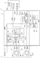
- FIG. 2 is a diagram illustrating a circuit configuration of the angle detection device 1 according to the first embodiment.
- the angle detection device 1 includes a magnetic detection unit 2 and an amplification unit 3.
- the magnetic detection unit 2 has a plurality of Hall elements for detecting the position of the rotor of the motor 20.
- the magnetic detection unit 2 will be described as having two Hall elements H1 and H2, and the first Hall element H1 and the second Hall element H2 have the same characteristics.
- Each Hall element H1, H2 can be equivalently represented by a bridge circuit composed of four internal resistances r1 to r4 as shown in FIG.
- the first Hall element H1 four nodes to which the internal resistors r1 to r4 are connected to each other are a first positive input terminal IP1, a first negative input terminal IN1, a first positive output terminal OP1, and a first node 1 Negative output terminal ON1.
- the second Hall element H2 four nodes to which the internal resistors r1 to r4 are connected to each other are a second positive input terminal IP2, a second negative input terminal IN2, and a second positive output terminal OP2.
- the second negative output terminal ON2 the second negative output terminal ON2.
- the plurality of Hall elements are connected in series with each other on the input side of each Hall element.
- the first Hall element H1 and the second Hall element H2 are connected in series between the power supply voltage VDD and the ground voltage GND on the respective input sides.
- the power supply voltage VDD is applied to the first positive input terminal IP1 of the first Hall element H1, and the first negative input terminal IN1 of the first Hall element H1
- the second positive input terminal IP2 of the second Hall element H2 is connected, and the ground voltage GND is applied to the second negative input terminal IN2 of the second Hall element H2.
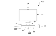
- FIG. 3A and 3B are diagrams illustrating an arrangement example of two Hall elements H1 and H2 in the first embodiment.
- FIG. 3A shows an arrangement example of two Hall elements H1 and H2 in the motor unit 100 when viewed from a direction perpendicular to the axis P of the output shaft 21 of the motor 20.
- FIG. 3B shows an arrangement example of two Hall elements H1 and H2 as viewed from the axial direction of the output shaft 21 of the motor 20 in the motor unit 100.
- a sensor magnet (magnet) 22 is provided on an output shaft 21 connected to a rotor (not shown) of the motor 20.
- the sensor magnet 22 is, for example, a disk-shaped two-pole permanent magnet.
- the sensor magnet 22 has, for example, a main surface 220 and a back surface 221 facing away from the main surface 220 as in the present embodiment. Further, the sensor magnet 22 has a through hole 222 that penetrates the main surface 220 and the back surface 221. The sensor magnet 22 is fixed to the output shaft 21 with the output shaft 21 passing through the through hole 222. The sensor magnet 22 rotates, for example, in the direction of reference sign R by the rotation of the rotor (output shaft 21) of the motor 20.
- the two Hall elements H1 and H2 are provided in the vicinity of the sensor magnet 22 at positions where the magnetic flux of the sensor magnet 22 can be detected with high accuracy. Specifically, as shown in FIGS. 3A and 3B, the two Hall elements H1 and H2 are arranged apart from each other along the direction R in which the sensor magnet 22 rotates (the rotation direction of the output shaft 21). . For example, the two Hall elements H1 and H2 face the side surface 223 of the sensor magnet 22 and are provided at positions whose phases are shifted by 90 degrees in the direction R in which the sensor magnet 22 rotates.
- the two Hall elements H1 and H2 detect the magnetic flux of the sensor magnet 22 due to the rotation of the output shaft 21 of the motor 20, and as an output signal an analog signal whose voltage changes in accordance with the change of the magnetic flux (hereinafter referred to as “Hall signal”). Are also output).
- the first Hall element H1 outputs a sine wave-shaped Hall signal 401 from the first positive output terminal OP1 and from the first negative output terminal ON1 to the Hall.
- a sinusoidal hall signal 402 having a polarity different from that of the signal 401 is output.
- the second hall element H2 outputs a sinusoidal hall signal 411 from the second positive output terminal OP2, and also outputs a sinusoidal hall signal having a polarity different from that of the hall signal 411 from the second negative output terminal ON2. 412 is output.
- the first Hall element H1 and the second Hall element H2 are arranged so as to be output from the first Hall element H1 by shifting their phases by 90 degrees in the direction R in which the sensor magnet 22 rotates.
- the signal pair (Hall signals 401 and 402) to be output and the signal pair (Hall signals 411 and 412) output from the second Hall element H2 are in a relationship of 90 degrees in phase.
- the control circuit 5 can calculate the absolute rotation angle of the rotor of the motor 20.
- the amplifying unit 3 is a functional unit that amplifies and outputs the Hall signals output from the two Hall elements H1 and H2.
- the amplifying unit 3 includes a first amplifying circuit 31 and a second amplifying circuit 32 that are provided for each of the two Hall elements H1 and H2 and amplify the Hall signal output from the corresponding Hall elements H1 and H2.
- the first amplifier circuit 31 is a circuit that amplifies the Hall signals 401 and 402 of the first Hall element H1. Specifically, the first amplifier circuit 31 includes a constant current source circuit 312 and a differential amplifier circuit 311.
- the constant current source circuit 312 is a circuit that generates a constant current and supplies it to the differential amplifier circuit 311.
- the constant current source circuit 312 includes, for example, P-type transistors Q13 and Q14 and a resistor R15.
- the P-type transistor is a transistor of a predetermined conductivity type, for example, a PNP junction bipolar transistor, a P-channel field effect transistor (for example, a P-channel MOS transistor), or the like.
- the P-type transistors Q13 and Q14 are PNP-type bipolar transistors.
- Transistor Q13 and transistor Q14 constitute a current mirror circuit.
- the base electrode and the collector electrode of the transistor Q13 are commonly connected, and the power supply voltage VDD is supplied to the emitter electrode of the transistor Q13.
- the power supply voltage VDD is a voltage output from the control circuit 5 as described above.
- One end of the resistor R15 is connected to the base electrode and the collector electrode of the transistor Q13, and the other end of the resistor R15 is supplied with the ground voltage GND.
- the power supply voltage VDD is supplied to the emitter electrode of the transistor Q14.
- the base electrode of the transistor Q14 is connected to one end of the resistor R15 together with the base electrode and the collector electrode of the transistor Q13.
- the collector electrode of the transistor Q14 is connected to a resistor R12 and a resistor R14 that constitute a differential input circuit 313 described later. Connected to the node.
- the differential amplifier circuit 311 includes a Hall signal 401 output from the first positive output terminal OP1 of the first Hall element H1, and a Hall signal 402 output from the first negative output terminal ON1 of the first Hall element H1. This circuit amplifies the difference between the two.
- the differential amplifier circuit 311 includes a differential input circuit 313 and resistors R11 to R14.
- the differential input circuit 313 includes, for example, a P-type (first conductivity type) transistor pair.
- the differential input circuit 313 includes PNP junction transistors (bipolar transistors) Q11 and Q12 as transistor pairs configured to have the same characteristics.
- the base electrode of the transistor Q11 is connected to the first negative output terminal ON1 of the first Hall element H1, and the base electrode of the transistor Q12 is connected to the first positive output terminal OP1 of the first Hall element H1.
- One end of the resistor R11 is connected to the collector electrode of the transistor Q11, and the other end of the resistor R11 is supplied with the ground voltage GND.
- One end of the resistor R13 is connected to the collector electrode of the transistor Q12, and the other end of the resistor R13 is supplied with the ground voltage GND.
- resistor R12 is connected to the emitter electrode of the transistor Q11.
- One end of the resistor R14 is connected to the emitter electrode of the transistor Q12.
- the other end of resistor R12 is connected to the other end of resistor R14 and the collector electrode of transistor Q14.
- differential amplifier circuit 311 having the above-described configuration, positive polarity amplification in which the difference between the Hall signal 401 and the Hall signal 402 is amplified from the node Np1 to which one end of the resistor R11 and the collector electrode of the transistor Q11 are connected.
- a signal 401A is output.
- a negative amplification signal 402A obtained by amplifying the difference between the Hall signal 401 and the Hall signal 402 is output from a node Nn1 to which one end of the resistor R13 and the collector electrode of the transistor Q12 are connected.
- the second amplifier circuit 32 is a circuit that amplifies the Hall signals 411 and 412 of the second Hall element H2. Specifically, the second amplifier circuit 32 includes a constant current source circuit 322 and a differential amplifier circuit 321.
- the constant current source circuit 322 is a circuit that generates a constant current and supplies it to the differential amplifier circuit 321.
- the constant current source circuit 322 includes, for example, N-type transistors Q23 and Q24 and a resistor R25.
- the N-type transistor is a transistor having a conductivity type opposite to that of the P-type transistor.
- an NPN junction bipolar transistor or an N-channel field effect transistor for example, an N-channel MOS transistor.
- the N-type transistors Q23 and Q24 are NPN-type bipolar transistors.
- Transistor Q23 and transistor Q24 form a current mirror circuit.
- the base electrode and the collector electrode of the transistor Q23 are commonly connected, and the ground voltage GND is supplied to the emitter electrode of the transistor Q23.
- One end of the resistor R25 is connected to the base electrode and the collector electrode of the transistor Q23, and the other end of the resistor R25 is supplied with the power supply voltage VDD.
- a ground voltage GND is supplied to the emitter electrode of the transistor Q24.
- the base electrode of the transistor Q24 is connected to one end of the resistor R25 together with the base electrode and the collector electrode of the transistor Q23.
- the collector electrode of the transistor Q24 is connected to a resistor R22 and a resistor R24 that constitute a differential input circuit 323 described later. Connected to the node.
- the differential amplifier circuit 321 includes a Hall signal 411 output from the second positive output terminal OP2 of the second Hall element H2, and a Hall signal 412 output from the second negative output terminal ON2 of the second Hall element H2. This circuit amplifies and outputs the difference.
- the differential amplifier circuit 321 includes a differential input circuit 323 and resistors R21 to R24.
- the differential input circuit 323 includes, for example, an N-type (second conductivity type) transistor pair.
- the differential input circuit 323 includes NPN junction bipolar transistors Q21 and Q22 as transistor pairs configured to have the same characteristics.
- the base electrode of the transistor Q21 is connected to the second negative output terminal ON2 of the second Hall element H2, and the base electrode of the transistor Q22 is connected to the second positive output terminal OP2 of the second Hall element H2.
- One end of the resistor R21 is connected to the collector electrode of the transistor Q21, and the other end of the resistor R21 is supplied with the power supply voltage VDD.
- One end of the resistor R23 is connected to the collector electrode of the transistor Q22, and the other end of the resistor R23 is supplied with the power supply voltage VDD.
- One end of the resistor R22 is connected to the emitter electrode of the transistor Q21.
- One end of resistor R24 is connected to the emitter electrode of transistor Q22.
- the other end of resistor R22 is connected to the other end of resistor R24 and the collector electrode of transistor Q24.
- differential amplifier circuit 321 having the above-described configuration, positive amplification in which the difference between the Hall signal 411 and the Hall signal 412 is amplified from the node Np2 to which one end of the resistor R21 and the collector electrode of the transistor Q21 are connected.
- a signal 411A is output.
- a negative amplified signal 412A obtained by amplifying the difference between the Hall signal 411 and the Hall signal 412 is output from a node Nn2 to which one end of the resistor R23 and the collector electrode of the transistor Q22 are connected.
- the Hall signals 401, 402, 411, and 412 of the Hall elements H1 and H2 are amplified by the amplifying unit 3 and input to the control circuit 5 as the amplified signals 401A, 402A, 411A, and 412A.
- the control circuit 5 calculates an actual measurement value of the rotation angle of the rotor of the motor 20 based on the input amplified signals 401A, 402A, 411A, 412A.
- the amplified signals 401A, 402A, 411A, and 412A (Hall signals 401, 402, 411, and 412) are generated by the two Hall elements H1 and H2 that are arranged at different positions in the rotation direction R of the sensor magnet 22. It is a signal based on the detected magnetic flux. Therefore, the control circuit 5 can calculate the absolute rotation angle of the rotor of the motor 20 by using the two amplified signals 401A and 402A and the amplified signals 411A and 412A having different phases.
- a known calculation method applied to an absolute rotary encoder or the like can be used as a method for calculating the absolute rotation angle of the rotor from two signals having different phases.
- a program relating to the calculation method is stored in the storage unit in the control circuit 5, and the control circuit 5 determines the absolute value of the rotor of the motor 20 based on the program and the amplified signals 401 A, 402 A, 411 A, 412 A.
- a simple rotation angle may be calculated.
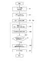
- FIG. 4 is a flowchart showing the flow of the motor control method in the motor unit 100 according to the first embodiment.
- step S1 when a power supply voltage is supplied to the motor unit 100, the motor unit 100 is activated (step S1). Next, each Hall element H1, H2 constituting the magnetic detection unit 2 of the angle detection device 1 detects the magnetic flux of the sensor magnet 22 fixed to the output shaft 21 of the motor 20, and the Hall signal 401 corresponding to the detected magnetic flux. , 402, 411, 412 are generated (step S2).
- the first amplifying circuit 31 and the second amplifying circuit 32 of the angle detection device 1 output the Hall signals 401, 402, 411, and 412 output from the corresponding first Hall element H1 and second Hall element H2, respectively.
- Amplified signals 401A, 402A, 411A, 412A are generated respectively (step S3).
- control device 4 executes a process for generating a drive signal for driving the motor 20 based on the amplified signals 401A, 402A, 411A, and 412A output from the angle detection device 1 (step S4). ).
- the control circuit 5 of the control device 4 reads the amplified signals 401A, 402A, 411A, 412A obtained by amplifying the Hall signals of the Hall elements H1, H2 (step S41).
- the control circuit 5 converts the amplified signals 401A, 402A, 411A, and 412A, which are analog signals, into digital signals by an analog / digital conversion circuit (not shown) provided in the control circuit 5, and performs control.
- the data is stored in a storage unit (not shown) provided inside the circuit 5.
- the control circuit 5 calculates an actual measurement value of the rotation angle of the rotor of the motor 20 based on the read amplified signals 401A, 402A, 411A, 412A (step S42).
- the first Hall element H1 and the second Hall element H2 are provided at positions shifted from each other in the rotation direction R of the sensor magnet 22 (for example, a position where the phase is shifted by 90 degrees). Therefore, the absolute rotation angle of the rotor can be calculated by using the amplified signals 401A, 402A, 411A, 412A based on the Hall signals of the two Hall elements H1, H2.
- control circuit 5 compares the target rotation angle set from the external device via the communication circuit 6 and the like with the measured value of the rotation angle of the rotor of the motor 20 calculated in step S42 (step S43). .
- step S43 when there is a difference between the target rotation angle and the measured value of the rotation angle, the control circuit 5 generates a drive control signal 8 so that the difference is reduced (step S44).
- the motor drive unit 7 generates drive signals (drive voltages) VA +, VA ⁇ , VB +, VB ⁇ based on the drive control signal 8 generated in step S44 and supplies them to each phase of the motor 20.
- the motor 20 is rotated (step S5). Thereby, the motor 20 is controlled to become the target rotation angle.
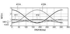
- 5A and 5B are diagrams showing simulation results of input signals and output signals of the first amplifier circuit 31 and the second amplifier circuit 32 in the angle detection apparatus 1 according to Embodiment 1.
- 5A and 5B the horizontal axis represents the rotation angle [deg] of the rotor, and the vertical axis represents the voltage [V].
- 5A shows Hall signals 401 and 402 of the first Hall element H1 as input signals of the first amplifier circuit 31, and amplified signals 401A and 402A as output signals of the first amplifier circuit 31.
- FIG. 5B shows Hall signals 411 and 412 of the second Hall element H2 as input signals of the second amplifier circuit 32, and amplified signals 411A and 412A as output signals of the second amplifier circuit 32.
- the Hall element when the detected magnetic flux is zero, that is, when the internal resistances r1 to r4 constituting the Hall element are in an equilibrium state (equal resistance values), the Hall element has a positive output Hall signal and a negative side.
- the output Hall signal has the same voltage. Therefore, the Hall signal output from the Hall element is based on the voltage when the internal resistances r1 to r4 are in an equilibrium state, for example, ⁇ 0.1 V to ⁇ 0 depending on the detected magnetic flux with the reference voltage as the center. It becomes an analog signal whose voltage changes in the range of .5V.
- the first Hall element H1 and the second Hall element H2 are connected to the power supply voltage VDD and the ground voltage GND on the respective input sides. Are connected in series with each other. Therefore, the reference voltage of the hall signal is a voltage obtained by dividing the voltage between the power supply voltage VDD and the ground voltage GND based on the resistance ratio of the internal resistances r1 to r4 of the hall elements H1 and H2.
- the reference voltage of the Hall signal of the first Hall element H1 is “VDD ⁇ 3/4”, and the second Hall element H2
- the reference voltage is “VDD ⁇ 1/4”.
- the Hall signals 401 and 402 of the first Hall element H1 have a waveform that changes up to about ⁇ 0.24V around 2.475V.
- the waveform changes up to about ⁇ 0.24V around the center.
- the second amplifier circuit 32 to which the Hall signals 411 and 412 of the second Hall element H2 are input includes a differential input circuit 323 including NPN transistors Q21 and Q22. If no signal is input, an appropriate amplification operation is not performed. For example, in order to properly operate the transistors Q21 and Q22, when the saturation voltage at the PN junction of the transistors Q21 and Q22 is VBE20 ( ⁇ 0.6 V), a voltage equal to or higher than “VBE20 ( ⁇ 0.6 V)” Must be input to the base electrodes of the transistors Q21 and Q22. On the other hand, when a large voltage near the power supply voltage VDD is input to the base electrodes of the transistors Q21 and Q22, the output voltage of the second amplifier circuit 32 is saturated.
- the first amplifier circuit 31 and the second amplifier circuit 32 that amplify the output signals from the first Hall element H1 and the second Hall element H2 have a limited input voltage range.
- the detection device 1 employs a configuration in which the first Hall element H1 and the second Hall element H2 are connected in series between the power supply voltage VDD and the ground voltage GND. It is possible to input a signal in an appropriate voltage range to the two amplifier circuit 32.
- the base electrode of the transistors Q11 and Q12 constituting the differential input stage of the first amplifier circuit 31 is changed by about ⁇ 0.24V at the maximum with 2.475V (VDD ⁇ 3/4) as the center.
- Hall signals 401 and 402 are input.
- the first amplifier circuit 31 can perform an appropriate amplification operation.
- amplified signals 401A and 402A obtained by linearly amplifying Hall signals 401 and 402 of the first Hall element H1 between a power supply voltage VDD (3.3V) and a ground voltage (0V). Can be generated.
- the base electrodes of the transistors Q21 and Q22 constituting the differential input stage of the second amplifier circuit 32 have a maximum of about ⁇ 0.24 V centered on 0.825 V (VDD ⁇ 1/4).
- Changing Hall signals 411 and 412 are input.
- the second amplifier circuit 32 can perform an appropriate amplification operation. For example, as shown in FIG. 5B, amplified signals 411A and 412A obtained by linearly amplifying the Hall signals 411 and 412 of the second Hall element H2 between the power supply voltage VDD (3.3 V) and the ground voltage (0 V). Can be generated.
- the base electrodes of the transistors Q11, Q12, Q21, and Q22 of the differential input circuits 313 and 323 of the first amplifier circuit 31 and the second amplifier circuit 32 are as small as possible within a range in which the transistors are opened. Since the suppressed voltage is applied, a current having an appropriate magnitude can be supplied to the differential input circuits 313 and 323. As a result, the power consumption of the first amplifier circuit 31 and the second amplifier circuit 32 can be suppressed.
- the resistance values (absolute values) of the internal resistances r1 to r4 of the two Hall elements H1 and H2 change due to the temperature change, but the resistance values of the internal resistances r1 to r4 of the two Hall elements H1 and H2 are Since it similarly changes with temperature, the resistance ratio of the internal resistances r1 to r4 of the first Hall element H1 and the second Hall element H2 does not change.
- the Hall signals 401, 402, 411, and 412 generated by dividing the voltage between the power supply voltage VDD and the ground voltage GND based on the resistance ratio of the internal resistors r1 to r4 are unlikely to vary with temperature. Become. This makes it possible to generate a hall signal that is highly stable with respect to temperature.
- the input voltage and the input current applied to the individual Hall elements H1 and H2 can be reduced.
- the same power supply as the operation power supply for example, 3.3 V
- MPU constituting the control circuit 5
- each Hall element H1, H2 has half of the operation power supply such as MPU. Is applied. Therefore, even a Hall element to which an input voltage of 3.3 V cannot be applied due to the specification can be adopted as the two Hall elements H1 and H2 of the angle detection device 1.
- a bridge circuit composed of the internal resistances r1 to r4 of the first Hall element H1 and a bridge circuit composed of the internal resistances r1 to r4 of the second Hall element H2 are connected in series between the power supply voltage VDD and the ground voltage GND. Therefore, the input current of each Hall element H1, H2 can be reduced. In order to further limit the input current, a separate resistor may be connected in series to the input side of the two Hall elements H1 and H2.
- two Hall elements H1 and H2 are connected in series, and the voltage applied to each Hall element H1 and H2 is made lower than the voltage between the power supply and the ground, so that the operation power supply for circuits other than the angle detection device 1 can be reduced. It can be used as a power source for the magnetic detection unit 2. As a result, it is not necessary to provide a separate power supply circuit only for driving the two Hall elements H1 and H2, so that an increase in circuit scale can be suppressed.
- the angle detection device 1 it is not necessary to use a commercially available high-precision operational amplifier IC, so that the cost can be reduced.
- the cost of the angle detection device 1 can be suppressed.
- circuit elements that require a high pair characteristic such as transistors that make up a differential input stage
- appropriate electronic components such as an IC in which multiple transistors with the same performance are housed in a single package, etc. It is preferable to use it.
- the angle detection device 1 According to the angle detection device 1 according to the present embodiment, various problems when the Hall element is employed are solved, and an inexpensive and highly accurate magnetic absolute angle sensor is provided. It becomes possible.
- FIG. 6 is a diagram illustrating a configuration of a motor unit according to the second embodiment.
- the motor unit 100A includes a motor 20A and a motor control device 10A.
- the motor 20A is, for example, a direct acting motor.
- the case where the motor 20 is a two-phase linear stepping motor having two phases of A phase and B phase will be described as an example.
- the motor control device 10A is configured to drive the motor 20A by supplying driving power to the motor 20A.
- the motor control device 10A includes a position detection device 1A and a control device 4A.
- the position detection device 1A is a device that generates and outputs a signal corresponding to the position of the output shaft 21A in accordance with the movement of the output shaft of the motor 20A.
- the control device 4A rotates the rotor of the motor 20A by applying a drive signal to the motor 20A based on a signal output from the position detection device 1A in accordance with the movement of the output shaft 21A of the motor 20A.
- the output shaft 21A moves linearly by the rotation of the rotor.
- the control device 4A includes a motor driving unit 7A that drives the motor 20A, a control circuit 5A that controls driving of the motor 20, and a communication circuit 6 that performs communication with an external device (not shown). doing.
- the constituent elements of the control device 4A shown in FIG. 1 are a part of the whole, and the control device 4A may have other constituent elements in addition to those shown in FIG. Good.
- the motor drive unit 7A based on the drive control signal 8A output from the control circuit 5A, drives signals (drive voltages) VA +, VA ⁇ , VB +, VB ⁇ for driving the coils of each phase constituting the motor 20A. Is supplied to each phase of the motor 20A.
- the control circuit 5A is configured by a program processing device such as MCU or DSP, for example.
- the entire control circuit 5A may be packaged as one integrated circuit device, or all or part of the control circuit 5A is packaged together with other devices to form one integrated circuit device. It may be configured.
- the control circuit 5A includes a command position signal (a signal indicating a target position of the output shaft 21A) set by an external device (user) via the communication circuit 6 and the like, and a motor 20A output from the position detection device 1A described later.
- the drive control signal 8A is generated based on the signals 411A and 412A indicating the position of the output shaft 21A, and the generated drive control signal 8A is supplied to the motor drive unit 7A. That is, the control circuit 5A generates a drive control signal 8A for driving the motor 20A while supplying feedback by comparing the target position with the actual value of the position of the output shaft 21A and supplies it to the motor drive unit 7A. Thus, the rotation control of the motor 20A is performed.
- the control circuit 5A has a function of outputting a fixed voltage that can be used as a power supply voltage for the peripheral circuit.
- the control circuit 5A operates with a power supply voltage of 3.3V, for example, and outputs a fixed voltage of 3.3V, for example, with the input power supply voltage as the power supply voltage VDD of the position detection device 1A.
- the position detection device 1A has a configuration in which a plurality of Hall elements as magnetic detection elements are connected in series to each other on the input side of each Hall element.
- the position detection device 1A is an absolute type sensor that can detect the absolute position of the output shaft 21A of the motor 20A based on the detection signal of the Hall element.
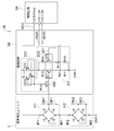
- FIG. 7 is a diagram illustrating a circuit configuration of the position detection device 1A. As illustrated in FIG. 7, the position detection device 1A includes a magnetic detection unit 2 and an amplifier circuit 3A.
- the second Hall element H2 is used for position detection of the output shaft 21A of the motor 20A.
- the first Hall element H1 is not used for detecting the position of the output shaft 21A, and is provided as a dummy element for compensating the characteristics of the second Hall element H2.
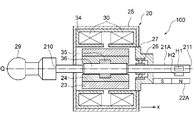
- FIG. 8A and 8B are diagrams showing an example of the arrangement of the two Hall elements H1 and H2.
- FIG. 8A shows an arrangement example of two Hall elements H1 and H2 when viewed from the direction perpendicular to the axis Q of the output shaft 21A of the motor 20A in the motor unit 100A.
- FIG. 8B shows an arrangement example of two Hall elements H1 and H2 as viewed from the direction of the axis Q of the output shaft 21A of the motor 20A in the motor unit 100A.
- the motor 20A includes a stator unit, a rotor unit, an output shaft 21A, a bearing 26, a cover 27, a case 25, and the like as components of the linear stepping motor. .
- FIGS. 3A and 3B only some components constituting the motor 20A are illustrated.
- the stator unit and the rotor unit are accommodated in the case 25.
- the stator unit includes a coil 30 and a stator yoke 34.
- the rotor unit includes a rotor magnet 23 and a rotor member 24.
- a female screw portion 35 is embedded in the rotor member 24.
- a male screw portion 36 is screwed inside the female screw portion 35.
- the output shaft 21 is disposed through the case 25.
- a head 29 as a driving target is fixed to one end portion 210 side of the output shaft 21.
- the female screw portion 35 and the male screw portion 36 formed on the rotor member 24 are engaged with each other, whereby the rotor member 24 and the output shaft 21 are connected.
- the female screw portion 35 embedded in the rotor member 24 also rotates.
- the male screw portion 36 meshed with the female screw portion 35 moves in the axial direction according to the same principle as the feeding mechanism using the ball screw, and as a result, the output shaft 21 moves in the direction of the axis P thereof. Move to. That is, in the motor 20, the rotational motion of the rotor unit is converted into the linear motion of the output shaft 21.
- two Hall elements H1 and H2 are fixed to the other end 211 side of the output shaft 21A. Thereby, when the output shaft 21A moves in the axis Q direction, the two Hall elements H1 and H2 also move in the axis Q direction.
- a sensor magnet (magnet) 22A is provided in the vicinity of the two Hall elements H1 and H2.
- the sensor magnet 22A is, for example, a rectangular plate-shaped two-pole permanent magnet.
- the sensor magnet 22A is fixed at a position facing the output shaft 21A. Specifically, the sensor magnet 22A is disposed at a position facing the second Hall element H2 in a direction perpendicular to the axis Q of the output shaft 21A. For example, as shown in FIGS. 8A and 8B, the sensor magnet 22A is disposed on the cover 27 that accommodates the bearing 26 that holds the end 211 side of the output shaft 21A so as to face the second Hall element H2. Yes. Thereby, when the output shaft 21A moves in the direction of the axis Q, the amount of magnetic flux detected by the sensor magnet 22A by the second Hall element H2 changes.
- the second Hall element H2 and the sensor magnet 22A are provided at a position where the second Hall element H2 can accurately detect the change in the magnetic flux of the sensor magnet 22A when the output shaft 21A is moved by the rotation of the motor 20A.
- the installation location of the second hall element H2 and the sensor magnet 22A is not limited to the example shown in FIGS. 8A and 8B.
- the second Hall element H2 detects the magnetic flux of the sensor magnet 22A and outputs an analog signal whose voltage changes in accordance with the change of the magnetic flux (hereinafter also referred to as “Hall signal”) as an output signal.
- the first Hall element H1 is a dummy element for compensating the characteristics of the second Hall element H2.
- the first Hall element H1 is preferably arranged in the vicinity of the second Hall element H2. That is, the first Hall element H1 is preferably disposed in a place where the same temperature environment as that of the second Hall element H2 is obtained.
- the first Hall element H1 and the second Hall element H2 have a phase in the outer peripheral direction of the output shaft 21A of 90 degrees (90 degrees on the outer peripheral surface of the output shaft 21A. The following are arranged so as to be shifted.
- circuit board or the like on which the amplifier circuit 3A and the like connected to the two Hall elements H1 and H2 are formed may be disposed in the case 25 of the motor 20A shown in FIGS. It may be arranged outside.
- the amplifier circuit 3A is a functional unit that amplifies and outputs the Hall signal output from the second Hall element H2.
- the amplifier circuit 3A is a circuit that amplifies the Hall signals 411 and 412 of the second Hall element H2.
- the amplifier circuit 3A includes a constant current source circuit 322 and a differential amplifier circuit 321.
- the constant current source circuit 322 is a circuit that generates a constant current and supplies it to the differential amplifier circuit 321.
- the constant current source circuit 322 includes, for example, N-type transistors Q23 and Q24 and a resistor R25.
- the N-type transistors Q23 and Q24 are NPN-type bipolar transistors.
- Transistor Q23 and transistor Q24 form a current mirror circuit.
- the base electrode and the collector electrode of the transistor Q23 are commonly connected, and the ground voltage GND is supplied to the emitter electrode of the transistor Q23.
- One end of the resistor R25 is connected to the base electrode and the collector electrode of the transistor Q23, and the other end of the resistor R25 is supplied with the power supply voltage VDD.
- a ground voltage GND is supplied to the emitter electrode of the transistor Q24.
- the base electrode of the transistor Q24 is connected to one end of the resistor R25 together with the base electrode and the collector electrode of the transistor Q23.
- the collector electrode of the transistor Q24 is connected to a resistor R22 and a resistor R24 that constitute a differential input circuit 323 described later. Connected to the node.
- the differential amplifier circuit 321 includes a Hall signal 411 output from the second positive output terminal OP2 of the second Hall element H2, and a Hall signal 412 output from the second negative output terminal ON2 of the second Hall element H2. This circuit amplifies and outputs the difference.
- the differential amplifier circuit 321 includes a differential input circuit 323 and resistors R21 to R24.
- the differential input circuit 323 includes, for example, an N-type (second conductivity type) transistor pair.
- the differential input circuit 323 includes NPN junction bipolar transistors Q21 and Q22 as transistor pairs configured to have the same characteristics.
- the base electrode of the transistor Q21 is connected to the second negative output terminal ON2 of the second Hall element H2, and the base electrode of the transistor Q22 is connected to the second positive output terminal OP2 of the second Hall element H2.
- One end of the resistor R21 is connected to the collector electrode of the transistor Q21, and the other end of the resistor R21 is supplied with the power supply voltage VDD.
- One end of the resistor R23 is connected to the collector electrode of the transistor Q22, and the other end of the resistor R23 is supplied with the power supply voltage VDD.
- One end of the resistor R22 is connected to the emitter electrode of the transistor Q21.
- One end of resistor R24 is connected to the emitter electrode of transistor Q22.
- the other end of resistor R22 is connected to the other end of resistor R24 and the collector electrode of transistor Q24.
- differential amplifier circuit 321 having the above-described configuration, positive amplification in which the difference between the Hall signal 411 and the Hall signal 412 is amplified from the node Np2 to which one end of the resistor R21 and the collector electrode of the transistor Q21 are connected.
- a signal 411A is output.
- a negative amplified signal 412A obtained by amplifying the difference between the Hall signal 411 and the Hall signal 412 is output from a node Nn2 to which one end of the resistor R23 and the collector electrode of the transistor Q22 are connected.
- the Hall signals 411 and 412 of the second Hall element H2 are amplified by the amplifier circuit 3A and input to the control circuit 5A as the amplified signals 411A and 412A.
- the control circuit 5A calculates an actual measurement value of the position of the output shaft 21A of the motor 20A based on the input amplified signals 411A and 412A.
- the amplified signals 411A and 412A are signals obtained by converting the magnitude of the magnetic flux that changes in accordance with the positional relationship between the sensor magnet 22A and the second Hall element H2 into a voltage. Therefore, the control circuit 5A can calculate the absolute position of the output shaft 21A of the motor 20A from the magnitudes of the voltages of the amplified signals 411A and 412A.
- a table or a relational expression representing the correspondence relationship between the voltage values of the amplified signals 411A and 412A and the position information of the output shaft 21A is stored in advance in the storage unit in the control circuit 5A, and the control circuit 5A
- the absolute position of the output shaft 21A of the motor 20A may be calculated based on the table, the relational expression, etc. stored in the above and the amplified signals 411A and 412A.
- FIG. 9 is a flowchart showing the flow of a motor control method in motor unit 100A according to the second embodiment.
- step S1A when a power supply voltage is supplied to the motor unit 100A, the motor unit 100A is activated.
- the second Hall element H2 provided on the output shaft 21A of the motor 20A detects the magnetic flux of the sensor magnet 22A, and generates Hall signals 411 and 412 corresponding to the detected magnetic flux (Step S2A).
- the amplification circuit 3A of the position detection device 1A amplifies the hall signals 411 and 412 output from the second hall element H2 to generate amplification signals 411A and 412A (step S3A).
- control device 4A executes processing for generating a drive signal for driving the motor 20A based on the amplified signals 411A and 412A output from the position detection device 1A (step S4A).
- the control circuit 5A of the control device 4A reads the amplified signals 411A and 412A obtained by amplifying the Hall signal of the second Hall element H2 (Step S41A).
- the control circuit 5A converts the amplified signals 411A and 412A, which are analog signals, into digital signals by an analog / digital conversion circuit (not shown) provided in the control circuit 5A. Is stored in a storage unit (not shown).
- control circuit 5A calculates an actual measurement value of the position of the output shaft 21A of the motor 20A based on the read amplified signals 411A and 412A (step S42A).
- Hall signals 411 and 412 amplified signals 411A and 412A
- the absolute position of the output shaft 21A can be calculated.
- control circuit 5A compares the target position set from the external device via the communication circuit 6 and the like with the actual measurement value of the position of the output shaft 21A of the motor 20A calculated in step S42A (step S43A). .
- step S43A when there is a deviation between the target position and the actually measured position, the control circuit 5A generates a drive control signal 8A so that the deviation width becomes small (step S44A).
- the motor drive unit 7A generates drive signals (drive voltages) VA +, VA ⁇ , VB +, VB ⁇ based on the drive control signal 8A generated in step S44A, and supplies the drive signals to each phase of the motor 20A.
- the motor 20A is rotated to move the output shaft 21A (step S5A).
- the motor 20A is controlled so that the output shaft 21A reaches the target position.
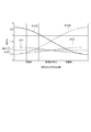
- FIG. 10 is a diagram illustrating simulation results of the input signal and the output signal of the amplifier circuit 3A in the position detection device according to the second embodiment.
- FIG. 10 also shows the hall signals 411 and 412 of the second hall element H2 as the input signal of the amplifier circuit 3A when the output shaft 21A of the motor 20A moves from the south pole side to the north pole side of the sensor magnet 22A. Amplified signals 411A and 412A as output signals of the amplifier circuit 3A are shown.
- the first Hall element H1 and the second Hall element H2 are connected to the power supply voltage VDD and the ground voltage GND on the input side, respectively. Are connected in series with each other. Therefore, the reference voltage of the hall signal of the second hall element H2 is obtained by dividing the voltage between the power supply voltage VDD and the ground voltage GND based on the resistance ratio of the internal resistances r1 to r4 of the hall elements H1 and H2. Voltage.
- the reference voltage of the Hall signal of the first Hall element H1 is “VDD ⁇ 3/4”, and the reference voltage of the Hall element H2 is “VDD ⁇ 1/4”.
- the Hall signals 411 and 412 of the second Hall element H2 have a waveform that changes about ⁇ 0.24V at the maximum around 0.825V.
- the amplifier circuit 3A to which the Hall signals 411 and 412 of the second Hall element H2 are input includes the differential input circuit 323 including NPN transistors Q21 and Q22. If it is not input, an appropriate amplification operation is not performed. For example, in order to properly operate the transistors Q21 and Q22, when the saturation voltage at the PN junction of the transistors Q21 and Q22 is VBE20 ( ⁇ 0.6 V), a voltage equal to or higher than “VBE20 ( ⁇ 0.6 V)” Must be input to the base electrodes of the transistors Q21 and Q22. On the other hand, when a large voltage near the power supply voltage VDD is input to the base electrodes of the transistors Q21 and Q22, the output voltage of the amplifier circuit 3A is saturated.
- the amplifier circuit 3A that amplifies the output signal from the Hall element has a limited input voltage range.
- the first Hall element H1, the second Hall element H2, and the like Adopts a configuration in which the power supply voltage VDD and the ground voltage GND are connected in series with each other, so that a signal in an appropriate voltage range can be input to the amplifier circuit 3A.
- the base electrodes of the transistors Q21 and Q22 constituting the differential input circuit 323 of the amplifier circuit 3A change by about ⁇ 0.24 V at the maximum centering on 0.825 V (VDD ⁇ 1/4).
- Hall signals 411 and 412 are input.
- the amplifier circuit 3A can perform an appropriate amplification operation.
- amplified signals 411A and 412A obtained by linearly amplifying the Hall signals 411 and 412 of the second Hall element H2 between the power supply voltage VDD (3.3 V) and the ground voltage (0 V). Can be generated.
- the differential input circuit 323 A current of an appropriate magnitude can be passed through. As a result, the power consumption of the amplifier circuit 3A can be suppressed.
- the voltage of the Hall signals 411 and 412 of the second Hall element H2 due to the temperature change by connecting the dummy Hall element H1 in series instead of using the second Hall element H2 used for magnetic detection alone. It becomes possible to suppress fluctuations. That is, the absolute values (resistance values) of the internal resistances r1 to r4 of the two Hall elements H1 and H2 connected in series vary with temperature, but the tendency of the change is between the internal resistances r1 to r4. Since the same is true, the resistance ratio of the internal resistances r1 to r4 of the first Hall element H1 and the second Hall element H2 does not change.
- the Hall signals 411 and 412 generated by dividing the voltage between the power supply voltage VDD and the ground voltage GND based on the resistance ratio of the internal resistances r1 to r4 of the first Hall element H1 and the second Hall element H2 are It becomes difficult to fluctuate with respect to temperature. This makes it possible to generate a hall signal that is highly stable with respect to temperature.
- the input voltage and the input current applied to the individual Hall elements H1 and H2 can be reduced.
- the operating power source for example, 3.3V
- MPU constituting the control circuit 5A
- each Hall element H1, H2 has half of the operating power source such as MPU. Is applied. Therefore, even a Hall element to which an input voltage of 3.3 V cannot be applied depending on the specification can be employed as the Hall elements H1 and H2 of the position detection device 1A.
- a bridge circuit composed of the internal resistances r1 to r4 of the first Hall element H1 and a bridge circuit composed of the internal resistances r1 to r4 of the second Hall element H2 are connected in series between the power supply voltage VDD and the ground voltage GND. Therefore, the input current of each Hall element H1, H2 can be reduced. In order to further limit the input current, a separate resistor may be connected in series to the input side of the two Hall elements H1 and H2.
- the position detection apparatus 1A it is not necessary to use a commercially available high-precision operational amplifier IC, so that the cost can be suppressed.
- the cost of the position detection device 1A can be reduced by adopting discrete components as circuit elements constituting the amplifier circuit 3A.
- circuit elements that require a high pair characteristic such as transistors that make up a differential input stage
- appropriate electronic components such as an IC in which multiple transistors with the same performance are housed in a single package, etc. It is preferable to use it.
- the installation locations of the sensor magnet 22 and the two Hall elements H1 and H2 are not limited to the positions shown in FIGS. 3A and 3B.
- the sensor magnet 22 only needs to be installed in a place where the magnetic flux of the sensor magnet 22 changes due to the rotation of the rotor of the motor 20, and the two Hall elements H1 and H2 change the magnetic flux of the sensor magnet 22. As long as it is installed in a location where it can be detected.
- the motor 20 is a two-phase stepping motor.
- a three-phase or five-phase stepping motor may be used, or another type of motor (for example, a brushless motor). Etc.).
- the present invention is not limited to this, and the first Hall element H1 is used to detect the sensor magnet 22A. Magnetic flux may be detected.
- FIGS. 8A and 8B the positions of the first Hall element H1 and the second Hall element H2 on the output shaft 21A are switched, and as shown in FIG. 11, the first positive output terminal OP1 of the first Hall element H1.
- the amplifier circuit 3B is preferably configured using a transistor having a polarity opposite to that of the above-described amplifier circuit 3A, that is, a P-type transistor.
- the differential input circuit 313 of the differential amplifier circuit 311 that receives Hall signals 401 and 402 having different polarities output from the first Hall element H1 is configured by a P-type transistor pair Q11 and Q12. It is preferable.
- the constant current source circuit 312 is preferably configured using a P-type transistor pair Q13, Q14.
- the amplifier circuits 31, 32, 3A, and 3B are not limited to the circuit configuration described above.
- the amplifier circuits 31, 32, 3A, and 3B may have any circuit configuration that can linearly amplify signals output from a plurality of Hall elements connected in series.
- the installation location of the sensor magnet 22A and the two hall elements H1 and H2 is not limited to the positions shown in FIGS. 8A and 8B. That is, one of the second Hall element H2 and the sensor magnet 22A is fixed to the output shaft 21A, and the other of the second Hall element H2 and the sensor magnet 22A is fixed to a position where it does not move according to the movement of the output shaft 21A. Just do it.
- the two Hall elements H1 and H2 and the sensor magnet 22A may be interchanged. That is, the two Hall elements H1 and H2 may be arranged on the cover 27, and the sensor magnet 22A may be fixed to the end 211 side of the output shaft 21A.
- the motor 20A is a two-phase linear stepping motor.
- the motor 20A is a direct acting motor, it can be applied to various motors.
- the motor 20A may be a three-phase or five-phase linear stepping motor, or may be another type of motor (for example, a brushless motor).
- the position detection device 1A is applied to a motor unit in order to detect the absolute position of the output shaft of the linear stepping motor is illustrated, but the application to be applied is not limited to the motor.
- the position detection device 1A can be applied to various applications in which the axis moves in the linear motion direction.
- SYMBOLS 1 Angle detection apparatus, 1A, 1B ... Position detection apparatus, 2 ... Magnetic detection unit, 3 ... Amplification part, 3A, 3B ... Amplification circuit, 4, 4A ... Control apparatus, 5, 5A ... Control circuit, 6 ... Communication circuit 7, 7A ... motor drive unit, 8, 8A ... drive control signal, 10, 10A ... motor controller, 20, 20A ... motor, 21, 21A ... output shaft, 22, 22A ... sensor magnet (magnet), 31 ... 1st amplifier circuit, 32 ... 2nd amplifier circuit, 100, 100A ... Motor unit, 311, 321 ... Differential amplifier circuit, 312, 322 ... Constant current source circuit, 313, 323 ...
- Differential input circuit 401, 402, 411, 412 ... Hall signal, 401A, 402A, 411A, 412A ... Amplified signal, GND ... Ground voltage, H1 ... First Hall element, H2 ... Second Hall element, IN1 ... First negative input terminal, IN2 ... Second Side input terminal, IP1 ... first positive input terminal, IP2 ... second positive input terminal, ON1 ... first negative output terminal, ON2 ... second negative output terminal, OP1 ... first positive output terminal, OP2 ... second positive output terminal, P ... axis, Q11 to Q14, Q21 to Q24 ... transistor, R ... rotation direction, r1 to r4 ... internal resistance, R11 to R15, R21 to R25 ... resistance, VDD ... power supply voltage.
Landscapes
- Engineering & Computer Science (AREA)
- Power Engineering (AREA)
- Physics & Mathematics (AREA)
- General Physics & Mathematics (AREA)
- Microelectronics & Electronic Packaging (AREA)
- Transmission And Conversion Of Sensor Element Output (AREA)
- Control Of Motors That Do Not Use Commutators (AREA)
- Measurement Of Length, Angles, Or The Like Using Electric Or Magnetic Means (AREA)
- Measuring Magnetic Variables (AREA)
- Control Of Electric Motors In General (AREA)
Abstract
ホール素子を用いて対象物の絶対的な位置を検出するための新たな技術を提供する。 磁気検出ユニット(2)は、2つのホール素子(第1ホール素子H1,第2ホール素子H2)を備える。2つのホール素子は、夫々のホール素子の入力側において、互いに直列に接続されている。
Description
本発明は、磁気検出ユニット、角度検出装置、位置検出装置、モータ制御装置、モータユニットおよびモータ制御方法に関し、例えば、モータのロータの移動角度を検出するための角度検出装置、当該角度検出装置によって検出した移動角度に基づいてモータを制御するモータ制御装置、リニアモータの出力軸の位置を検出するための位置検出装置、および当該位置検出装置によって検出した位置情報に基づいてモータを制御するモータ制御装置に関する。
一般的なステッピングモータでは、ロータの相対的な回転角度(移動角度)を検出することは容易である一方で、ロータの絶対的な回転角度、例えば、モータを動作させる前の初期状態における回転角度を検出することは容易ではない。
従来、ステッピングモータの絶対的な回転角度を検出するための方法として、ステッピングモータの出力軸にアブソリュート型の角度センサを取り付けることによって、角度検出を行う手法が知られている。例えば、特許文献1には、ステッピングモータのロータの位置を検出するためのアブソリュート型のエンコーダが設けられたモータ制御装置が開示されている。
また、一般的に、リニアモータ等の出力軸が直線的に移動する直動型モータにおいて、出力軸の絶対的な位置を検出するためには、別途、位置検出用センサを取り付ける必要がある。例えば、特許文献1には、直動型モータの出力軸の位置を検出する位置検出器として、光学式エンコーダが設けられたリニアアクチュエータが開示されている。
アブソリュート型の角度センサのセンサ方式としては、主に、光学式および磁気式が知られている。また、直動型モータの出力軸の位置を検出する位置検出器のセンサ方式としては、上述した光学式と磁気式が知られている。一般に、光学式の角度センサ(光学式エンコーダ)は、価格が非常に高いという課題がある。
そこで、本願発明者らは、ステッピングモータに搭載するアブソリュート型の角度センサやリニアモータに搭載する位置検出器として、光学式の角度センサよりも安価な角度センサ、すなわちホール素子を用いた角度センサを採用することを検討した。
しかしながら、角度センサにホール素子を採用した場合であっても種々の課題がある。例えば、ホール素子は、温度によってホール素子の内部抵抗が変化するため(例えば、100Ω~2000Ω)、ホール素子の出力信号の電圧が安定しないという課題がある。また、ホール素子は、印加可能な最大入力電流または最大入力電圧が低いという課題がある。例えば、あるホール素子は、-40℃~120℃の範囲において、最大で10mAまでしか印加できない。更に、ホール素子は、その出力電圧の幅(出力電圧幅)が微小であるという課題がある。例えば、±40mTの磁束を検知した場合、ホール素子の出力電圧幅は±0.24Vである。
上述したホール素子の課題を解決するために、ホール素子と、ホール素子の出力信号を増幅する高精度なオペアンプICとを組み合わせた製品が市販されている。しかしながら、このような製品は非常に高価であるとともに、消費電力が大きいという課題がある。
本発明は、上述した課題に鑑みてなされたものであり、ホール素子を用いて対象物の絶対的な位置を検出するための新たな技術を提供することを目的とする。
本発明の代表的な実施の形態に係る磁気検出ユニットは、複数のホール素子を備え、前記複数のホール素子は、夫々の前記ホール素子の入力側において、互いに直列に接続されていることを特徴とする。
本発明に係る角度検出装置によれば、ホール素子を用いて対象物の絶対的な位置を検出するための新たな技術を提供することが可能となる。
1.実施の形態の概要
先ず、本願において開示される発明の代表的な実施の形態について概要を説明する。なお、以下の説明では、一例として、発明の構成要素に対応する図面上の参照符号を、括弧を付して記載している。
先ず、本願において開示される発明の代表的な実施の形態について概要を説明する。なお、以下の説明では、一例として、発明の構成要素に対応する図面上の参照符号を、括弧を付して記載している。
〔1〕本発明の代表的な実施の形態に係る磁気検出ユニット(2)は、複数のホール素子(H1,H2)を備え、前記複数のホール素子は、夫々の前記ホール素子の入力側において、互いに直列に接続されていることを特徴とする。
〔2〕上記〔1〕に記載の磁気検出ユニットにおいて、前記複数のホール素子は、第1正側入力端子(IP1)および第1負側入力端子(IN1)と第1正側出力端子(OP1)および第1負側出力端子(ON1)とを有する第1ホール素子(H1)と、第2正側入力端子(IP2)および第2負側入力端子(IN2)と第2正側出力端子(OP2)および第2負側出力端子(ON2)とを有する第2ホール素子(H2)と、を含み、前記第1ホール素子の前記第1正側入力端子に電源電圧(VDD)が印加され、前記第1ホール素子の前記第1負側入力端子と前記第2ホール素子の前記第2正側入力端子とが接続され、前記第2ホール素子の前記第2負側入力端子にグランド電圧(GND)が印加されていてもよい。
〔3〕本発明の代表的な実施の形態に係る角度検出装置(1)は、上記〔2〕に記載の磁気検出ユニット(2)と、前記ホール素子毎に設けられ、対応する前記ホール素子の出力信号(401,402,411,412)を増幅する複数の増幅回路(31,32)とを備えることを特徴とする。
〔4〕上記〔3〕に記載の角度検出装置において、前記複数の増幅回路は、前記第1ホール素子における前記第1正側出力端子の電圧と前記第1負側出力端子の電圧との差を増幅する第1増幅回路(31)と、前記第2ホール素子における前記第2正側出力端子の電圧と前記第2負側出力端子の電圧との差を増幅する第2増幅回路(32)とを含み、前記第1増幅回路は、P型のトランジスタ対(Q11,Q12)を含む差動入力回路(313)を有し、前記第2増幅回路は、N型のトランジスタ対(Q21,Q22)を含む差動入力回路(323)を有していてもよい。
〔5〕本発明の代表的な実施の形態に係るモータ制御装置は、上記〔3〕または〔4〕に記載の角度検出装置(1)と、前記複数の増幅回路によってそれぞれ増幅された信号(401A,402A,411A,412A)に基づいて、モータの駆動を制御するための駆動制御信号(8)を生成する制御装置(4)と、を含むことを特徴とする。
〔6〕本発明の代表的な実施の形態に係るモータユニットは、上記〔5〕に記載のモータ制御装置(10)と、前記制御装置によって生成された前記駆動制御信号に基づいて制御される前記モータ(20)と、前記モータの出力軸(21)に設けられた磁石(22)とを備え、前記複数のホール素子は、前記磁石が回転する方向(R)に沿って互いに離間して配置されていることを特徴とする。
〔7〕上記〔6〕に記載のモータユニットにおいて、前記ホール素子を2つ有し、当該2つの前記ホール素子は、前記磁石が回転する方向に沿って位相が90度ずつずれるように配置されていてもよい。
〔8〕本発明の代表的な実施の形態に係る位置検出装置(1A/1B)は、上記〔2〕に記載の磁気検出ユニット(2)と、前記複数のホール素子のうち一つのホール素子(H2/H1)の出力信号(411,412/401,402)を増幅する増幅回路(3A/3B)とを備え、前記複数のホール素子は、夫々の前記ホール素子の入力側において、互いに直列に接続されていることを特徴とする。
〔9〕上記〔8〕に記載の位置検出装置において、前記増幅回路は、前記第2ホール素子における前記第2正側出力端子の電圧と前記第2負側出力端子の電圧との差を増幅し、前記増幅回路は、N型のトランジスタ対(Q21,Q22)を含む差動入力回路(323)を有していてもよい。
〔10〕本発明の代表的な実施の形態に係る別のモータ制御装置(10A)は、上記〔8〕または〔9〕に記載の位置検出装置(1A)と、前記増幅回路によって増幅された信号に基づいて、モータ(20A)の駆動を制御するための駆動制御信号(8A)を生成する制御装置(4A)と、を含むことを特徴とする。
〔11〕本発明の代表的な実施の形態に係る別のモータユニット(100A)は、上記〔10〕に記載のモータ制御装置(10A)と、前記モータと、磁石(22A)とを備え、前記モータは、出力軸(21A)を有し、前記駆動制御信号に基づいて前記出力軸の軸線(Q)方向への移動が制御される直動型モータであって、前記一つのホール素子および前記磁石の一方が、前記出力軸に固定され、前記一つのホール素子および前記磁石の他方が、前記出力軸と対向する位置に固定されていてもよい。
〔12〕上記〔11〕に記載のモータユニットにおいて、前記一つのホール素子は、前記出力軸に固定され、前記磁石は、前記出力軸に対向する位置に固定されていてもよい。
〔13〕本発明の代表的な実施の形態に係る方法は、モータのロータの回転に応じて回転する磁石の磁束を検出するための複数のホール素子(H1,H2)と、前記ホール素子毎に設けられた複数の増幅回路(31,32)と、モータ(20)の駆動を制御するための駆動制御信号(8)を生成する制御装置(4)とを備え、前記複数のホール素子がそれぞれの入力側において互いに直列に接続されているモータ制御装置(10)を用いたモータ制御方法であって、前記ホール素子が、検出した磁束に応じて前記出力信号を生成するステップ(S2)と、前記複数の増幅回路が、対応する前記ホール素子によって生成された前記出力信号をそれぞれ増幅するステップ(S3)と、前記制御装置が、夫々の前記増幅回路によって増幅された信号に基づいて前記ロータの回転角度を算出し、算出した回転角度に基づいて前記駆動制御信号を生成して前記モータに供給するステップ(S4)と、を含むことを特徴とする。
〔14〕本発明の代表的な実施の形態に係る方法は、入力側において互いに直列に接続された複数のホール素子(H1,H2)を有する磁気検出ユニット(2)と、増幅回路(3A)と、磁石(22A)と、出力軸(21A)がその軸線(P)方向に移動可能な直動型モータ(20A)の駆動を制御するための駆動制御信号(8A)を生成する制御装置(4A)とを有し、前記複数のホール素子および前記磁石の一方が前記出力軸の移動に応じて移動する位置に設けられ、前記複数のホール素子および前記磁石の他方が前記出力軸に対向する位置に設けられたモータ制御装置(10A)を用いたモータ制御方法であって、前記複数のホール素子のうち一つのホール素子が、検出した磁束に応じた信号(411,412)を生成するステップ(S2A)と、前記増幅回路が、前記一つのホール素子(H2)によって生成された信号(411,412)を増幅するステップ(S3A)と、前記制御装置が、前記増幅回路によって増幅された信号に基づいて前記出力軸の位置を算出し、算出した位置に基づいて前記駆動制御信号を生成して前記直動型モータに供給するステップ(S4A)とを含むことを特徴とする。
2.実施の形態の具体例
以下、本発明の実施の形態の具体例について図を参照して説明する。なお、以下の説明において、各実施の形態において共通する構成要素には同一の参照符号を付し、繰り返しの説明を省略する。また、図面は模式的なものであり、各要素の寸法の関係、各要素の比率などは、現実と異なる場合があることに留意する必要がある。図面の相互間においても、互いの寸法の関係や比率が異なる部分が含まれている場合がある。
以下、本発明の実施の形態の具体例について図を参照して説明する。なお、以下の説明において、各実施の形態において共通する構成要素には同一の参照符号を付し、繰り返しの説明を省略する。また、図面は模式的なものであり、各要素の寸法の関係、各要素の比率などは、現実と異なる場合があることに留意する必要がある。図面の相互間においても、互いの寸法の関係や比率が異なる部分が含まれている場合がある。
≪実施の形態1≫
〈モータユニット〉
図1は、実施の形態1に係るモータユニットの構成を示す図である。
図1に示されるように、モータユニット100は、モータ20と、モータ制御装置10とを有する。
〈モータユニット〉
図1は、実施の形態1に係るモータユニットの構成を示す図である。
図1に示されるように、モータユニット100は、モータ20と、モータ制御装置10とを有する。
モータ20は、例えばステッピングモータである。本実施の形態では、モータ20が、A相とB相の2つの相を有する2相ステッピングモータである場合を例にとり、説明する。
モータ制御装置10は、モータ20に駆動電力を供給してモータ20を駆動させるように構成されている。具体的に、モータ制御装置10は、角度検出装置1と制御装置4とを有する。角度検出装置1は、モータ20のロータの回転に応じて、ロータの回転位置に対応する信号を生成して出力する装置である。制御装置4は、モータ20のロータの回転に応じて角度検出装置1から出力される信号に基づいて、モータ20に駆動信号を印加することで、モータ20を回転させる。
〈制御装置〉
制御装置4は、モータ20を駆動させるモータ駆動部7と、モータ20の駆動を制御する制御回路5と、外部装置(図示せず)との間で通信を行うための通信回路6とを有している。なお、図1に示されている制御装置4の構成要素は、全体の一部であり、制御装置4は、図1に示されたものに加えて、他の構成要素を有していてもよい。
制御装置4は、モータ20を駆動させるモータ駆動部7と、モータ20の駆動を制御する制御回路5と、外部装置(図示せず)との間で通信を行うための通信回路6とを有している。なお、図1に示されている制御装置4の構成要素は、全体の一部であり、制御装置4は、図1に示されたものに加えて、他の構成要素を有していてもよい。
モータ駆動部7は、制御回路5から出力された駆動制御信号8に基づいて、モータ20を構成する各相のコイルを駆動するための駆動信号(駆動電圧)VA+,VA-,VB+,VB-を生成し、モータ20の各相に供給する。
制御回路5は、例えば、MCU(Microprogram Control Unit)やDSP(Digital Signal Processor)等のプログラム処理装置によって構成されている。なお、制御回路5は、その全体が1つの集積回路装置としてパッケージ化されていてもよいし、他の装置と一緒に制御回路5の全部又は一部がパッケージ化されて1つの集積回路装置が構成されていてもよい。
制御回路5は、通信回路6等を経由して外部装置(ユーザ)から設定される指令回転角度信号(目標回転角度に応じた信号)と、後述する角度検出装置1から出力されるモータ20の回転角度を示す信号401A,402A,411A,412Aとに基づいて駆動制御信号8を生成し、生成された駆動制御信号8をモータ駆動部7に供給する。すなわち、制御回路5は、目標回転角度と、モータ20の回転角度の実測値との比較でフィードバックをかけながら、モータ20を駆動させるための駆動制御信号8を生成してモータ駆動部7に供給することにより、モータ20の回転制御を行う。
また、制御回路5は、周辺回路の電源電圧として利用可能な固定電圧を出力する機能を有している。制御回路5は、例えば3.3Vの電源電圧が供給されて動作するとともに、入力された電源電圧を角度検出装置1の電源電圧VDDとして、例えば、3.3Vの固定電圧を出力する。
〈角度検出装置〉
角度検出装置1は、磁気検出素子としての複数のホール素子が、それぞれのホール素子の入力側において互いに直列に接続された構成を有している。角度検出装置1は、複数のホール素子の検出信号に基づいてモータ20のロータの絶対的な回転角度を検出可能なアブソリュート型の角度センサである。
角度検出装置1は、磁気検出素子としての複数のホール素子が、それぞれのホール素子の入力側において互いに直列に接続された構成を有している。角度検出装置1は、複数のホール素子の検出信号に基づいてモータ20のロータの絶対的な回転角度を検出可能なアブソリュート型の角度センサである。
図2は、実施の形態1に係る角度検出装置1の回路構成を示す図である。
図2に示すように、角度検出装置1は、磁気検出ユニット2と増幅部3とを有する。
図2に示すように、角度検出装置1は、磁気検出ユニット2と増幅部3とを有する。
(1)磁気検出ユニット
磁気検出ユニット2は、モータ20のロータの位置を検出するための複数のホール素子を有する。本実施の形態では、一例として、磁気検出ユニット2が2つのホール素子H1、H2を有し、第1ホール素子H1と第2ホール素子H2とが同一の特性を有するものとして、説明する。
磁気検出ユニット2は、モータ20のロータの位置を検出するための複数のホール素子を有する。本実施の形態では、一例として、磁気検出ユニット2が2つのホール素子H1、H2を有し、第1ホール素子H1と第2ホール素子H2とが同一の特性を有するものとして、説明する。
各ホール素子H1,H2は、図2に示すような4つの内部抵抗r1~r4から成るブリッジ回路で等価的に表すことができる。第1ホール素子H1において、各内部抵抗r1~r4が互いに接続される4つのノードがそれぞれ、第1正側入力端子IP1、第1負側入力端子IN1、第1正側出力端子OP1、および第1負側出力端子ON1となる。同様に、第2ホール素子H2において、各内部抵抗r1~r4が互いに接続される4つのノードがそれぞれ、第2正側入力端子IP2、第2負側入力端子IN2、第2正側出力端子OP2、および第2負側出力端子ON2となる。
磁気検出ユニット2において、複数のホール素子は、それぞれのホール素子の入力側において互いに直列に接続されている。具体的に、第1ホール素子H1と第2ホール素子H2とは、それぞれの入力側において、電源電圧VDDとグランド電圧GNDとの間に互いに直列に接続されている。
より具体的には、図2に示すように、第1ホール素子H1の第1正側入力端子IP1に電源電圧VDDが印加されるとともに、第1ホール素子H1の第1負側入力端子IN1と第2ホール素子H2の第2正側入力端子IP2とが接続され、第2ホール素子H2の第2負側入力端子IN2にグランド電圧GNDが印加される。
図3A,図3Bは、実施の形態1における2つのホール素子H1,H2の配置例を示す図である。
図3Aには、モータユニット100において、モータ20の出力軸21の軸線Pに垂直な方向から見たときの2つのホール素子H1,H2の配置例が示されている。図3Bには、モータユニット100において、モータ20の出力軸21の軸線方向から見た2つのホール素子H1,H2の配置例が示されている。
図3Aには、モータユニット100において、モータ20の出力軸21の軸線Pに垂直な方向から見たときの2つのホール素子H1,H2の配置例が示されている。図3Bには、モータユニット100において、モータ20の出力軸21の軸線方向から見た2つのホール素子H1,H2の配置例が示されている。
図3A,3Bに示すように、モータユニット100において、モータ20のロータ(図示せず)と連結された出力軸21にセンサマグネット(磁石)22が設けられている。センサマグネット22は、例えば、円板状の2極の永久磁石である。
センサマグネット22は、例えば、本実施形態のように、主面220と主面220に背向する裏面221とを有する。更に、センサマグネット22は、主面220と裏面221とを貫通する貫通孔222を有する。センサマグネット22は、貫通孔222に出力軸21が貫通した状態で、出力軸21に固定されている。センサマグネット22は、モータ20のロータ(出力軸21)の回転により、例えば参照符号Rの方向に回転する。
2つのホール素子H1,H2は、センサマグネット22の近傍において、センサマグネット22の磁束を精度良く検出可能な位置に設けられている。具体的には、図3A,3Bに示すように、2つのホール素子H1,H2は、センサマグネット22が回転する方向(出力軸21の回転方向)Rに沿って互いに離間して配置されている。例えば、2つのホール素子H1,H2は、センサマグネット22の側面223に対面し、センサマグネット22が回転する方向Rに位相が90度ずれた位置にそれぞれ設けられている。
2つのホール素子H1,H2は、モータ20の出力軸21の回転によるセンサマグネット22の磁束を検出し、出力信号として、磁束の変化に応じて電圧が変化するアナログ信号(以下、「ホール信号」とも称する。)を出力する。
例えば、出力軸21が一定の速度で回転したとき、第1ホール素子H1は、第1正側出力端子OP1から正弦波状のホール信号401を出力するとともに、第1負側出力端子ON1から、ホール信号401と極性の異なる正弦波状のホール信号402を出力する。同様に、第2ホール素子H2は、第2正側出力端子OP2から正弦波状のホール信号411を出力するとともに、第2負側出力端子ON2から、ホール信号411と極性の異なる正弦波状のホール信号412を出力する。
例えば、出力軸21が一定の速度で回転したとき、第1ホール素子H1は、第1正側出力端子OP1から正弦波状のホール信号401を出力するとともに、第1負側出力端子ON1から、ホール信号401と極性の異なる正弦波状のホール信号402を出力する。同様に、第2ホール素子H2は、第2正側出力端子OP2から正弦波状のホール信号411を出力するとともに、第2負側出力端子ON2から、ホール信号411と極性の異なる正弦波状のホール信号412を出力する。
図3A,3Bに示すように、第1ホール素子H1と第2ホール素子H2とをセンサマグネット22が回転する方向Rに互いに位相を90度ずらして配置することにより、第1ホール素子H1から出力される信号対(ホール信号401,402)と第2ホール素子H2から出力される信号対(ホール信号411,412)とは、位相が90度ずれた関係となる。この互いに位相が異なるホール信号401,402およびホール信号411,412を用いることにより、制御回路5は、モータ20のロータの絶対的な回転角度を算出することが可能となる。
(2)増幅部
図2に示すように、増幅部3は、2つのホール素子H1,H2から出力されたホール信号をそれぞれ増幅して出力する機能部である。増幅部3は、2つのホール素子H1,H2毎に設けられ、対応するホール素子H1,H2から出力されたホール信号を増幅する第1増幅回路31,第2増幅回路32を有する。
図2に示すように、増幅部3は、2つのホール素子H1,H2から出力されたホール信号をそれぞれ増幅して出力する機能部である。増幅部3は、2つのホール素子H1,H2毎に設けられ、対応するホール素子H1,H2から出力されたホール信号を増幅する第1増幅回路31,第2増幅回路32を有する。
第1増幅回路31は、第1ホール素子H1のホール信号401,402をそれぞれ増幅する回路である。具体的に、第1増幅回路31は、定電流源回路312と差動増幅回路311とを有する。
定電流源回路312は、定電流を発生して、差動増幅回路311に供給する回路である。定電流源回路312は、例えば、P型のトランジスタQ13,Q14と抵抗R15とを含む。
ここで、P型のトランジスタとは、所定の導電型のトランジスタであり、例えば、PNP接合のバイポーラトランジスタや、Pチャネル型の電界効果トランジスタ(例えば、Pチャネル型のMOSトランジスタ)等である。
例えば、P型のトランジスタQ13,Q14は、PNP型のバイポーラトランジスタである。トランジスタQ13とトランジスタQ14とはカレントミラー回路を構成している。
定電流源回路312において、トランジスタQ13のベース電極とコレクタ電極とが共通に接続され、トランジスタQ13のエミッタ電極は、電源電圧VDDが供給される。ここで、電源電圧VDDは、上述したように制御回路5から出力された電圧である。
抵抗R15の一端は、トランジスタQ13のベース電極およびコレクタ電極に接続され、抵抗R15の他端は、グランド電圧GNDが供給される。トランジスタQ14のエミッタ電極は、電源電圧VDDが供給される。トランジスタQ14のベース電極は抵抗R15の一端にトランジスタQ13のベース電極およびコレクタ電極とともに接続され、トランジスタQ14のコレクタ電極は、後述する差動入力回路313を構成する抵抗R12と抵抗R14とが互いに接続されるノードに接続される。
上述した構成を有する定電流源回路312によれば、トランジスタQ13のベース・エミッタ間電圧をVBE13としたとき、Ip=(VDD-VBE13)/R15の電流IpがトランジスタQ13から出力され、その電流Ipをコピーした電流がトランジスタQ14から差動増幅回路311に供給される。
差動増幅回路311は、第1ホール素子H1の第1正側出力端子OP1から出力されたホール信号401と、第1ホール素子H1の第1負側出力端子ON1から出力されたホール信号402との差を増幅する回路である。
差動増幅回路311は、差動入力回路313と、抵抗R11~R14とを含む。
差動入力回路313は、例えば、P型(第1導電型)のトランジスタ対を含む。例えば、差動入力回路313は、互いに特性が等しくなるように構成されたトランジスタ対として、PNP接合のトランジスタ(バイポーラトランジスタ)Q11,Q12を有している。
差動入力回路313は、例えば、P型(第1導電型)のトランジスタ対を含む。例えば、差動入力回路313は、互いに特性が等しくなるように構成されたトランジスタ対として、PNP接合のトランジスタ(バイポーラトランジスタ)Q11,Q12を有している。
トランジスタQ11のベース電極は、第1ホール素子H1の第1負側出力端子ON1と接続され、トランジスタQ12のベース電極は、第1ホール素子H1の第1正側出力端子OP1と接続される。
抵抗R11の一端は、トランジスタQ11のコレクタ電極に接続され、抵抗R11の他端は、グランド電圧GNDが供給される。抵抗R13の一端は、トランジスタQ12のコレクタ電極に接続され、抵抗R13の他端は、グランド電圧GNDが供給される。
抵抗R12の一端は、トランジスタQ11のエミッタ電極に接続される。抵抗R14の一端は、トランジスタQ12のエミッタ電極に接続される。抵抗R12の他端は、抵抗R14の他端とトランジスタQ14のコレクタ電極とに接続される。
上述した構成を有する差動増幅回路311によれば、抵抗R11の一端とトランジスタQ11のコレクタ電極とが接続されるノードNp1から、ホール信号401とホール信号402との差を増幅した正極性の増幅信号401Aが出力される。また、抵抗R13の一端とトランジスタQ12のコレクタ電極とが接続されるノードNn1から、ホール信号401とホール信号402との差を増幅した負極性の増幅信号402Aが出力される。
第2増幅回路32は、第2ホール素子H2のホール信号411,412をそれぞれ増幅する回路である。具体的に、第2増幅回路32は、定電流源回路322と差動増幅回路321とを有する。
定電流源回路322は、定電流を発生して、差動増幅回路321に供給する回路である。定電流源回路322は、例えば、N型のトランジスタQ23,Q24と抵抗R25とを含む。
ここで、N型のトランジスタとは、P型のトランジスタとは反対の導電型のトランジスタであり、例えば、NPN接合のバイポーラトランジスタや、Nチャネル型の電界効果トランジスタ(例えば、Nチャネル型のMOSトランジスタ)等である。
例えば、N型のトランジスタQ23,Q24は、NPN型のバイポーラトランジスタである。トランジスタQ23とトランジスタQ24とはカレントミラー回路を構成している。
定電流源回路322において、トランジスタQ23のベース電極とコレクタ電極とが共通に接続され、トランジスタQ23のエミッタ電極は、グランド電圧GNDが供給される。
抵抗R25の一端は、トランジスタQ23のベース電極およびコレクタ電極に接続され、抵抗R25の他端は、電源電圧VDDが供給される。トランジスタQ24のエミッタ電極は、グランド電圧GNDが供給される。トランジスタQ24のベース電極は抵抗R25の一端にトランジスタQ23のベース電極およびコレクタ電極とともに接続され、トランジスタQ24のコレクタ電極は、後述する差動入力回路323を構成する抵抗R22と抵抗R24とが互いに接続されるノードに接続される。
上述した構成を有する定電流源回路322によれば、トランジスタQ23のベース・エミッタ間電圧をVBE23としたとき、電流In=(VDD-VBE23)/R25がトランジスタQ23から出力され、その電流Inをコピーした電流がトランジスタQ24から差動増幅回路321に供給される。
差動増幅回路321は、第2ホール素子H2の第2正側出力端子OP2から出力されたホール信号411と、第2ホール素子H2の第2負側出力端子ON2から出力されたホール信号412との差を増幅して出力する回路である。
差動増幅回路321は、差動入力回路323と、抵抗R21~R24とを含む。差動入力回路323は、例えば、N型(第2導電型)のトランジスタ対を含む。例えば、差動入力回路323は、互いに特性が等しくなるように構成されたトランジスタ対として、NPN接合のバイポーラトランジスタQ21,Q22を有している。
トランジスタQ21のベース電極は、第2ホール素子H2の第2負側出力端子ON2と接続され、トランジスタQ22のベース電極は、第2ホール素子H2の第2正側出力端子OP2と接続される。
抵抗R21の一端は、トランジスタQ21のコレクタ電極に接続され、抵抗R21の他端は、電源電圧VDDが供給される。抵抗R23の一端は、トランジスタQ22のコレクタ電極に接続され、抵抗R23の他端は、電源電圧VDDが供給される。抵抗R22の一端は、トランジスタQ21のエミッタ電極に接続される。抵抗R24の一端は、トランジスタQ22のエミッタ電極に接続される。抵抗R22の他端は、抵抗R24の他端とトランジスタQ24のコレクタ電極とに接続される。
上述した構成を有する差動増幅回路321によれば、抵抗R21の一端とトランジスタQ21のコレクタ電極とが接続されるノードNp2から、ホール信号411とホール信号412との差を増幅した正極性の増幅信号411Aが出力される。また、抵抗R23の一端とトランジスタQ22のコレクタ電極とが接続されるノードNn2から、ホール信号411とホール信号412との差を増幅した負極性の増幅信号412Aが出力される。
このように、各ホール素子H1,H2のホール信号401,402,411,412は、増幅部3によって増幅され、増幅信号401A,402A,411A,412Aとして制御回路5に入力される。
制御回路5は、入力された増幅信号401A,402A,411A,412Aに基づいて、モータ20のロータの回転角度の実測値を算出する。上述したように、増幅信号401A,402A,411A,412A(ホール信号401,402,411,412)は、センサマグネット22の回転方向Rに互いに異なる位置に配置された2つのホール素子H1,H2によって検出された磁束に基づく信号である。したがって、互いに位相の異なる2つの増幅信号401A,402Aおよび増幅信号411A,412Aを用いることにより、制御回路5は、モータ20のロータの絶対的な回転角度を算出することが可能となる。
なお、互いに位相の異なる2つの信号からロータの絶対的な回転角度を算出する方法は、アブソリュート型のロータリエンコーダ等に適用されている公知の計算方法を用いることができる。例えば、その計算方法に関するプログラムを制御回路5内の記憶部に記憶しておき、制御回路5が、そのプログラムと増幅信号401A,402A,411A,412Aとに基づいて、モータ20のロータの絶対的な回転角度を算出すればよい。
〈モータ制御方法〉
次に、モータユニット100におけるモータ20の制御方法について説明する。
図4は、実施の形態1に係るモータユニット100におけるモータ制御方法の流れを示すフロー図である。
次に、モータユニット100におけるモータ20の制御方法について説明する。
図4は、実施の形態1に係るモータユニット100におけるモータ制御方法の流れを示すフロー図である。
先ず、モータユニット100に電源電圧が供給されると、モータユニット100が起動する(ステップS1)。次に、角度検出装置1の磁気検出ユニット2を構成する各ホール素子H1,H2がモータ20の出力軸21に固定されたセンサマグネット22の磁束を検出し、検出した磁束に応じたホール信号401,402,411,412を生成する(ステップS2)。
次に、角度検出装置1の第1増幅回路31,第2増幅回路32が、それぞれに対応する第1ホール素子H1,第2ホール素子H2から出力されたホール信号401,402,411,412をそれぞれ増幅して、増幅信号401A,402A,411A,412Aを生成する(ステップS3)。
次に、制御装置4が、角度検出装置1から出力された増幅信号401A,402A,411A,412Aに基づいて、モータ20を駆動するための駆動信号を生成するための処理を実行する(ステップS4)。
具体的には、先ず、制御装置4の制御回路5が、各ホール素子H1,H2のホール信号を増幅した増幅信号401A,402A,411A,412Aを読み取る(ステップS41)。例えば、制御回路5が、制御回路5の内部に設けられたアナログ/デジタル変換回路(図示せず)により、アナログ信号である増幅信号401A,402A,411A,412Aをデジタル信号に変換して、制御回路5の内部に設けられた記憶部(図示せず)に記憶する。
次に、制御回路5が、読み取った増幅信号401A,402A,411A,412Aに基づいて、モータ20のロータの回転角度の実測値を算出する(ステップS42)。このとき、第1ホール素子H1と第2ホール素子H2とは、上述したように、センサマグネット22の回転方向Rに互いにずれた位置(例えば、位相が90度ずれた位置)に設けられているので、2つのホール素子H1,H2のホール信号に基づく増幅信号401A,402A,411A,412Aを用いることにより、ロータの絶対的な回転角度を算出することが可能となる。
次に、制御回路5が、通信回路6等を経由して外部装置から設定された目標回転角度と、ステップS42で算出したモータ20のロータの回転角度の実測値とを比較する(ステップS43)。ステップS43において、目標回転角度と回転角度の実測値との差がある場合には、制御回路5は、その差が小さくなるような駆動制御信号8を生成する(ステップS44)。
次に、モータ駆動部7は、ステップS44において生成された駆動制御信号8に基づいて、駆動信号(駆動電圧)VA+,VA-,VB+,VB-を生成し、モータ20の各相に供給してモータ20を回転させる(ステップS5)。これにより、モータ20は、目標回転角度となるよう制御される。
〈角度検出装置の効果〉
図5A,図5Bは、実施の形態1に係る角度検出装置1における第1増幅回路31,第2増幅回路32の入力信号および出力信号のシミュレーション結果を示す図である。このシミュレーションでは、電源電圧VDD=3.3V、グランド電圧GND=0Vとしている。
図5A,図5Bは、実施の形態1に係る角度検出装置1における第1増幅回路31,第2増幅回路32の入力信号および出力信号のシミュレーション結果を示す図である。このシミュレーションでは、電源電圧VDD=3.3V、グランド電圧GND=0Vとしている。
図5A,5Bにおいて、横軸はロータの回転角度〔deg〕を表し、縦軸は電圧〔V〕を表している。また、図5Aには、第1増幅回路31の入力信号としての第1ホール素子H1のホール信号401,402と、第1増幅回路31の出力信号としての増幅信号401A,402Aとが示されている。図5Bには、第2増幅回路32の入力信号としての第2ホール素子H2のホール信号411,412と、第2増幅回路32の出力信号としての増幅信号411A,412Aとが示されている。
一般に、ホール素子は、検出される磁束がゼロであるとき、すなわちホール素子を構成する各内部抵抗r1~r4が平衡状態(互いに等しい抵抗値)であるとき、正側出力のホール信号と負側出力のホール信号とは同電圧となる。そのため、ホール素子から出力されるホール信号は、内部抵抗r1~r4が平衡状態にあるときの電圧を基準とし、その基準電圧を中心に、検出した磁束に応じて例えば±0.1V~±0.5Vの範囲で電圧が変化するアナログ信号となる。
実施の形態1に係る角度検出装置1では、上述したように、磁気検出ユニット2において第1ホール素子H1と第2ホール素子H2とが、それぞれの入力側において、電源電圧VDDとグランド電圧GNDとの間で互いに直列に接続されている。そのため、ホール信号の基準電圧は、各ホール素子H1,H2の内部抵抗r1~r4の抵抗比に基づいて、電源電圧VDDとグランド電圧GNDとの間の電圧を分圧した電圧となる。すなわち、2つのホール素子H1,H2の各内部抵抗r1~r4が平衡状態にあるとき、第1ホール素子H1のホール信号の基準電圧は”VDD×3/4”となり、第2ホール素子H2の基準電圧は、”VDD×1/4”となる。
例えば、図5Aに示すように、電源電圧VDD=3.3V、グランド電圧GND=0Vとしたとき、第1ホール素子H1の基準電圧は、2.475V(=3.3×3/4)となり、第1ホール素子H1のホール信号401,402は、2.475Vを中心に最大約±0.24V変化する波形となる。同様に、図5Bに示すように、第2ホール素子H2の基準電圧は0.825V(=3.3×1/4)となり、第2ホール素子H2のホール信号411,412は、0.825Vを中心に最大約±0.24V変化する波形となる。
一方、第1ホール素子H1のホール信号401,402が入力される第1増幅回路31は、PNP型のトランジスタQ11,Q12から成る差動入力回路313を有しているので、適切な電圧範囲の信号が入力されないと、適切な増幅動作を行わない。例えば、トランジスタQ11,Q12を適切に動作させるためには、トランジスタQ11,Q12のPN接合部の飽和電圧をVBE10(≒0.6V)としたとき、”VDD-VBE10(≒3.3-0.6=2.7V)”以下の電圧をトランジスタQ11,Q12のベース電極に入力する必要がある。その一方で、トランジスタQ11,Q12のベース電極にグランド電圧GND付近の小さな電圧を入力した場合、第1増幅回路31の出力電圧が飽和してしまう。
同様に、第2ホール素子H2のホール信号411,412が入力される第2増幅回路32は、NPN型のトランジスタQ21,Q22から成る差動入力回路323を有しているので、適切な電圧範囲の信号が入力されないと、適切な増幅動作を行わない。例えば、トランジスタQ21,Q22を適切に動作させるためには、トランジスタQ21,Q22のPN接合部の飽和電圧をVBE20(≒0.6V)としたとき、”VBE20(≒0.6V)”以上の電圧をトランジスタQ21,Q22のベース電極に入力する必要がある。その一方で、トランジスタQ21,Q22のベース電極に電源電圧VDD付近の大きな電圧を入力した場合、第2増幅回路32の出力電圧は飽和してしまう。
このように第1ホール素子H1,第2ホール素子H2からの出力信号を増幅する第1増幅回路31,第2増幅回路32には入力電圧範囲に制限があるが、本実施の形態に係る角度検出装置1では、第1ホール素子H1と第2ホール素子H2とが電源電圧VDDとグランド電圧GNDとの間で互いに直列に接続された構成を採用しているので、第1増幅回路31,第2増幅回路32に適切な電圧範囲の信号を入力することが可能となる。
例えば、第1増幅回路31の差動入力段を構成するトランジスタQ11,Q12のベース電極には、上述したように、2.475V(VDD×3/4)を中心に最大約±0.24V変化するホール信号401,402が入力される。これにより、第1増幅回路31は適切な増幅動作を行うことができる。例えば、図5Aに示すように、電源電圧VDD(3.3V)とグランド電圧(0V)との間で、第1ホール素子H1のホール信号401,402をリニアに増幅させた増幅信号401A,402Aを生成することができる。
同様に、第2増幅回路32の差動入力段を構成するトランジスタQ21,Q22のベース電極には、上述したように、0.825V(VDD×1/4)を中心に最大約±0.24V変化するホール信号411,412が入力される。これにより、第2増幅回路32は適切な増幅動作を行うことができる。例えば、図5Bに示すように、電源電圧VDD(3.3V)とグランド電圧(0V)との間で、第2ホール素子H2のホール信号411,412をリニアに増幅させた増幅信号411A,412Aを生成することができる。
また、このように、第1増幅回路31,第2増幅回路32の差動入力回路313,323のトランジスタQ11,Q12、Q21,Q22のベース電極には、トランジスタが開放される範囲内で極力小さく抑えた電圧が印加されるので、差動入力回路313,323に適切な大きさの電流を流すことができる。これにより、第1増幅回路31,第2増幅回路32の消費電力を抑えることが可能となる。
また、第1ホール素子H1と第2ホール素子H2とが直列に接続された構成を採用することにより、温度の変化による、ホール信号401,402,411,412の電圧変動を抑えることが可能となる。すなわち、温度の変化により、2つのホール素子H1,H2の各内部抵抗r1~r4の抵抗値(絶対値)は変化するが、2つのホール素子H1,H2の内部抵抗r1~r4の抵抗値は温度に対して同様に変化するため、第1ホール素子H1および第2ホール素子H2の内部抵抗r1~r4の抵抗比は変化しない。したがって、電源電圧VDDとグランド電圧GNDとの間の電圧を内部抵抗r1~r4の抵抗比に基づいて分圧して生成されるホール信号401,402,411,412は、温度に対して変動し難くなる。これにより、温度に対する安定性の高いホール信号を生成することが可能となる。
また、第1ホール素子H1と第2ホール素子H2とが直列に接続された構成を採用することにより、個々のホール素子H1,H2に印加される入力電圧および入力電流を小さくすることができる。例えば、制御回路5を構成しているMPU等の動作電源(例えば3.3V)と同じ電源を磁気検出ユニット2に供給する場合、各ホール素子H1,H2には、MPU等の動作電源の半分の電圧が印加される。そのため、仕様により3.3Vの入力電圧を印加することができないホール素子であっても、角度検出装置1の2つのホール素子H1,H2として採用することが可能となる。
また、第1ホール素子H1の内部抵抗r1~r4から成るブリッジ回路と第2ホール素子H2の内部抵抗r1~r4から成るブリッジ回路とが電源電圧VDDとグランド電圧GNDとの間に直列に接続されるので、各ホール素子H1,H2の入力電流を小さくすることが可能となる。なお、入力電流を更に制限したい場合には、2つのホール素子H1,H2の入力側に直列に別途抵抗を接続してもよい。
また、2つのホール素子H1,H2を直列に接続して各ホール素子H1,H2に印加される電圧を電源-グランド間の電圧よりも下げることにより、角度検出装置1以外の回路の動作電源を磁気検出ユニット2の電源として利用することが可能となる。これにより、2つのホール素子H1,H2を駆動するためだけに、別途、電源回路を設ける必要がないので、回路規模の増大を抑えることが可能となる。
また、本実施の形態に係る角度検出装置1によれば、市販されている高精度なオペアンプICを用いる必要がないので、コストを抑えることが可能となる。例えば、第1増幅回路31,第2増幅回路32を構成する回路素子としてディスクリート部品を採用することにより、角度検出装置1のコストを抑えることができる。ただし、差動入力段を構成するトランジスタ等、特性の高いペア性が要求される回路素子については、適切な電子部品、たとえば同じ性能を有する複数のトランジスタが一つのパッケージに収められたIC等を用いる方が好ましい。
以上説明したように、本実施の形態に係る角度検出装置1によれば、ホール素子を採用した場合の種々の課題を解決し、安価で高精度な磁気式のアブソリュート型の角度センサを提供することが可能となる。
≪実施の形態2≫
〈モータユニット〉
図6は、実施の形態2に係るモータユニットの構成を示す図である。
図6に示されるように、モータユニット100Aは、モータ20Aと、モータ制御装置10Aとを有する。
〈モータユニット〉
図6は、実施の形態2に係るモータユニットの構成を示す図である。
図6に示されるように、モータユニット100Aは、モータ20Aと、モータ制御装置10Aとを有する。
モータ20Aは、例えば、直動型モータである。本実施の形態では、モータ20が、A相とB相の2つの相を有する2相リニアステッピングモータである場合を例にとり、説明する。
モータ制御装置10Aは、モータ20Aに駆動電力を供給してモータ20Aを駆動させるように構成されている。具体的に、モータ制御装置10Aは、位置検出装置1Aと制御装置4Aとを有する。位置検出装置1Aは、モータ20Aの出力軸の移動に応じて、出力軸21Aの位置に対応する信号を生成して出力する装置である。制御装置4Aは、モータ20Aの出力軸21Aの移動に応じて位置検出装置1Aから出力される信号に基づいて、モータ20Aに駆動信号を印加することで、モータ20Aのロータを回転させる。ロータの回転により、出力軸21Aが直動する。
〈制御装置〉
制御装置4Aは、モータ20Aを駆動させるモータ駆動部7Aと、モータ20の駆動を制御する制御回路5Aと、外部装置(図示せず)との間で通信を行うための通信回路6とを有している。なお、図1に示されている制御装置4Aの構成要素は、全体の一部であり、制御装置4Aは、図6に示されたものに加えて、他の構成要素を有していてもよい。
制御装置4Aは、モータ20Aを駆動させるモータ駆動部7Aと、モータ20の駆動を制御する制御回路5Aと、外部装置(図示せず)との間で通信を行うための通信回路6とを有している。なお、図1に示されている制御装置4Aの構成要素は、全体の一部であり、制御装置4Aは、図6に示されたものに加えて、他の構成要素を有していてもよい。
モータ駆動部7Aは、制御回路5Aから出力された駆動制御信号8Aに基づいて、モータ20Aを構成する各相のコイルを駆動するための駆動信号(駆動電圧)VA+,VA-,VB+,VB-を生成し、モータ20Aの各相に供給する。
制御回路5Aは、例えば、MCUやDSP等のプログラム処理装置によって構成されている。なお、制御回路5Aは、その全体が1つの集積回路装置としてパッケージ化されていてもよいし、他の装置と一緒に制御回路5Aの全部又は一部がパッケージ化されて1つの集積回路装置が構成されていてもよい。
制御回路5Aは、通信回路6等を経由して外部装置(ユーザ)から設定される指令位置信号(出力軸21Aの目標位置を示す信号)と、後述する位置検出装置1Aから出力されるモータ20Aの出力軸21Aの位置を示す信号411A,412Aとに基づいて駆動制御信号8Aを生成し、生成された駆動制御信号8Aをモータ駆動部7Aに供給する。すなわち、制御回路5Aは、目標位置と、出力軸21Aの位置の実測値との比較でフィードバックをかけながら、モータ20Aを駆動させるための駆動制御信号8Aを生成してモータ駆動部7Aに供給することにより、モータ20Aの回転制御を行う。
また、制御回路5Aは、周辺回路の電源電圧として利用可能な固定電圧を出力する機能を有している。制御回路5Aは、例えば3.3Vの電源電圧が供給されて動作するとともに、入力された電源電圧を位置検出装置1Aの電源電圧VDDとして、例えば、3.3Vの固定電圧を出力する。
〈位置検出装置〉
位置検出装置1Aは、磁気検出素子としての複数のホール素子が、それぞれのホール素子の入力側において互いに直列に接続された構成を有している。位置検出装置1Aは、ホール素子の検出信号に基づいてモータ20Aの出力軸21Aの絶対的な位置を検出可能なアブソリュート型のセンサである。
位置検出装置1Aは、磁気検出素子としての複数のホール素子が、それぞれのホール素子の入力側において互いに直列に接続された構成を有している。位置検出装置1Aは、ホール素子の検出信号に基づいてモータ20Aの出力軸21Aの絶対的な位置を検出可能なアブソリュート型のセンサである。
図7は、位置検出装置1Aの回路構成を示す図である。
図7に示すように、位置検出装置1Aは、磁気検出ユニット2と増幅回路3Aとを有する。
図7に示すように、位置検出装置1Aは、磁気検出ユニット2と増幅回路3Aとを有する。
磁気検出ユニット2において、2つのホール素子H1,H2のうち、第2ホール素子H2は、モータ20Aの出力軸21Aの位置検出に用いられる。一方、第1ホール素子H1は、出力軸21Aの位置検出に用いられず、第2ホール素子H2の特性を補償するためのダミー素子として設けられている。
図8A,図8Bは、2つのホール素子H1,H2の配置例を示す図である。
図8Aには、モータユニット100Aにおいて、モータ20Aの出力軸21Aの軸線Qに垂直な方向から見たときの2つのホール素子H1,H2の配置例が示されている。図8Bには、モータユニット100Aにおいて、モータ20Aの出力軸21Aの軸線Q方向から見た2つのホール素子H1,H2の配置例が示されている。
図8Aには、モータユニット100Aにおいて、モータ20Aの出力軸21Aの軸線Qに垂直な方向から見たときの2つのホール素子H1,H2の配置例が示されている。図8Bには、モータユニット100Aにおいて、モータ20Aの出力軸21Aの軸線Q方向から見た2つのホール素子H1,H2の配置例が示されている。
図8A,8Bに示すように、モータユニット100Aにおいて、モータ20Aはリニアステッピングモータの構成要素として、ステータユニット、ロータユニット、出力軸21A、ベアリング26、カバー27、およびケース25等を有している。なお、図3A,3Bには、モータ20Aを構成する一部の構成要素のみを図示している。
モータ20Aにおいて、ステータユニットおよびロータユニットがケース25内に収容されている。ステータユニットは、コイル30およびステータヨーク34を含んでいる。ロータユニットは、ロータマグネット23とロータ部材24を含んでいる。ロータ部材24には、雌螺子部35が埋め込まれている。また、雌螺子部35の内側には、雄螺子部36が螺合している。出力軸21は、ケース25を貫通した状態で配置されている。出力軸21の一方の端部210側には、駆動対象としてのヘッド29が固定されている。
ケース25内において、ロータ部材24に形成された雌螺子部35と雄螺子部36とが噛み合うことにより、ロータ部材24と出力軸21とが連結されている。ロータユニットが回転すると、ロータ部材24に埋め込まれた雌螺子部35も回転する。雌螺子部35が回転すると、雌螺子部35に噛み合った雄螺子部36がボールねじを利用した送り機構と同様の原理により、軸方向に移動し、その結果、出力軸21がその軸線P方向に移動する。すなわち、モータ20では、ロータユニットの回転運動が出力軸21の直線運動に変換される。
図8Aに示すように、出力軸21Aの他方の端部211側には、2つのホール素子H1,H2が固定されている。これにより、出力軸21Aが軸線Q方向に移動したとき、2つのホール素子H1,H2も軸線Q方向に移動する。
2つのホール素子H1,H2の近傍には、センサマグネット(磁石)22Aが設けられている。センサマグネット22Aは、例えば、矩形の板状の2極の永久磁石である。
センサマグネット22Aは、出力軸21Aに対向する位置に固定されている。具体的に、センサマグネット22Aは、出力軸21Aの軸線Qに垂直な方向において、第2ホール素子H2と対向する位置に配置されている。例えば、図8A,図8Bに示すように、センサマグネット22Aは、出力軸21Aの端部211側を保持するベアリング26を収容するカバー27上に、第2ホール素子H2と対向して配置されている。これにより、出力軸21Aが軸線Q方向に移動したときに、第2ホール素子H2によるセンサマグネット22Aの磁束の検出量が変化する。
なお、第2ホール素子H2およびセンサマグネット22Aは、モータ20Aの回転によって出力軸21Aが移動したときに、第2ホール素子H2がセンサマグネット22Aの磁束の変化を精度良く検出可能な位置に設けられていればよく、第2ホール素子H2およびセンサマグネット22Aの設置場所は、図8A,8Bに示す例に限定されない。
第2ホール素子H2は、センサマグネット22Aの磁束を検出し、出力信号として、磁束の変化に応じて電圧が変化するアナログ信号(以下、「ホール信号」とも称する。)を出力する。
第1ホール素子H1は、上述したように、第2ホール素子H2の特性を補償するためのダミー素子である。第1ホール素子H1は、第2ホール素子H2の近傍に配置することが好ましい。すなわち、第1ホール素子H1は、第2ホール素子H2と同じ温度環境となる場所に配置することが好ましい。例えば、図8A,8Bに示すように、例えば、第1ホール素子H1と第2ホール素子H2とは、出力軸21Aの外周面上において、出力軸21Aの外周方向の位相が90度(90度以下)ずれるように配置される。
なお、2つのホール素子H1,H2と接続される増幅回路3A等が形成された回路基板等は、図8A,8Bに示されるモータ20Aのケース25内に配置されてもよいし、ケース25の外部に配置されていてもよい。
(2)増幅回路
図7に示すように、増幅回路3Aは、第2ホール素子H2から出力されたホール信号をそれぞれ増幅して出力する機能部である。
増幅回路3Aは、第2ホール素子H2のホール信号411,412をそれぞれ増幅する回路である。具体的に、増幅回路3Aは、定電流源回路322と差動増幅回路321とを有する。
図7に示すように、増幅回路3Aは、第2ホール素子H2から出力されたホール信号をそれぞれ増幅して出力する機能部である。
増幅回路3Aは、第2ホール素子H2のホール信号411,412をそれぞれ増幅する回路である。具体的に、増幅回路3Aは、定電流源回路322と差動増幅回路321とを有する。
定電流源回路322は、定電流を発生して、差動増幅回路321に供給する回路である。定電流源回路322は、例えば、N型のトランジスタQ23,Q24と抵抗R25とを含む。
例えば、N型のトランジスタQ23,Q24は、NPN型のバイポーラトランジスタである。トランジスタQ23とトランジスタQ24とはカレントミラー回路を構成している。
定電流源回路322において、トランジスタQ23のベース電極とコレクタ電極とが共通に接続され、トランジスタQ23のエミッタ電極は、グランド電圧GNDが供給される。
抵抗R25の一端は、トランジスタQ23のベース電極およびコレクタ電極に接続され、抵抗R25の他端は、電源電圧VDDが供給される。トランジスタQ24のエミッタ電極は、グランド電圧GNDが供給される。トランジスタQ24のベース電極は抵抗R25の一端にトランジスタQ23のベース電極およびコレクタ電極とともに接続され、トランジスタQ24のコレクタ電極は、後述する差動入力回路323を構成する抵抗R22と抵抗R24とが互いに接続されるノードに接続される。
上述した構成を有する定電流源回路322によれば、トランジスタQ23のベース・エミッタ間電圧をVBE23としたとき、電流In=(VDD-VBE23)/R25がトランジスタQ23から出力され、その電流Inをコピーした電流がトランジスタQ24から差動増幅回路321に供給される。
差動増幅回路321は、第2ホール素子H2の第2正側出力端子OP2から出力されたホール信号411と、第2ホール素子H2の第2負側出力端子ON2から出力されたホール信号412との差を増幅して出力する回路である。
差動増幅回路321は、差動入力回路323と、抵抗R21~R24とを含む。差動入力回路323は、例えば、N型(第2導電型)のトランジスタ対を含む。例えば、差動入力回路323は、互いに特性が等しくなるように構成されたトランジスタ対として、NPN接合のバイポーラトランジスタQ21,Q22を有している。
トランジスタQ21のベース電極は、第2ホール素子H2の第2負側出力端子ON2と接続され、トランジスタQ22のベース電極は、第2ホール素子H2の第2正側出力端子OP2と接続される。
抵抗R21の一端は、トランジスタQ21のコレクタ電極に接続され、抵抗R21の他端は、電源電圧VDDが供給される。抵抗R23の一端は、トランジスタQ22のコレクタ電極に接続され、抵抗R23の他端は、電源電圧VDDが供給される。抵抗R22の一端は、トランジスタQ21のエミッタ電極に接続される。抵抗R24の一端は、トランジスタQ22のエミッタ電極に接続される。抵抗R22の他端は、抵抗R24の他端とトランジスタQ24のコレクタ電極と接続される。
上述した構成を有する差動増幅回路321によれば、抵抗R21の一端とトランジスタQ21のコレクタ電極とが接続されるノードNp2から、ホール信号411とホール信号412との差を増幅した正極性の増幅信号411Aが出力される。また、抵抗R23の一端とトランジスタQ22のコレクタ電極とが接続されるノードNn2から、ホール信号411とホール信号412との差を増幅した負極性の増幅信号412Aが出力される。
このように、第2ホール素子H2のホール信号411,412は、増幅回路3Aによって増幅され、増幅信号411A,412Aとして制御回路5Aに入力される。
制御回路5Aは、入力された増幅信号411A,412Aに基づいて、モータ20Aの出力軸21Aの位置の実測値を算出する。上述したように、増幅信号411A,412A(ホール信号411,412)は、センサマグネット22Aと第2ホール素子H2との位置関係に応じて変化する磁束の大きさを電圧に変換した信号である。したがって、制御回路5Aは、増幅信号411A,412Aの電圧の大きさから、モータ20Aの出力軸21Aの絶対的な位置を算出することが可能となる。例えば、増幅信号411A,412Aの電圧値と出力軸21Aの位置情報との対応関係を表すテーブルや関係式等を制御回路5A内の記憶部に予め記憶しておき、制御回路5Aが、記憶部に記憶されたそのテーブルや関係式等と増幅信号411A,412Aとに基づいて、モータ20Aの出力軸21Aの絶対的な位置を算出すればよい。
〈モータ制御方法〉
次に、実施の形態2に係るモータユニット100Aにおけるモータ20Aの制御方法について説明する。
図9は、実施の形態2に係るモータユニット100Aにおけるモータ制御方法の流れを示すフロー図である。
次に、実施の形態2に係るモータユニット100Aにおけるモータ20Aの制御方法について説明する。
図9は、実施の形態2に係るモータユニット100Aにおけるモータ制御方法の流れを示すフロー図である。
先ず、モータユニット100Aに電源電圧が供給されると、モータユニット100Aが起動する(ステップS1A)。次に、モータ20Aの出力軸21Aに設けられた第2ホール素子H2がセンサマグネット22Aの磁束を検出し、検出した磁束に応じたホール信号411,412を生成する(ステップS2A)。
次に、位置検出装置1Aの増幅回路3Aが、第2ホール素子H2から出力されたホール信号411,412をそれぞれ増幅して、増幅信号411A,412Aを生成する(ステップS3A)。
次に、制御装置4Aが、位置検出装置1Aから出力された増幅信号411A,412Aに基づいて、モータ20Aを駆動するための駆動信号を生成するための処理を実行する(ステップS4A)。
具体的には、先ず、制御装置4Aの制御回路5Aが、第2ホール素子H2のホール信号を増幅した増幅信号411A,412Aを読み取る(ステップS41A)。例えば、制御回路5Aが、制御回路5Aの内部に設けられたアナログ/デジタル変換回路(図示せず)により、アナログ信号である増幅信号411A,412Aをデジタル信号に変換して、制御回路5Aの内部に設けられた記憶部(図示せず)に記憶する。
次に、制御回路5Aが、読み取った増幅信号411A,412Aに基づいて、モータ20Aの出力軸21Aの位置の実測値を算出する(ステップS42A)。このとき、出力軸21Aに固定された第2ホール素子H2とセンサマグネット22との位置関係に応じて電圧が変化する第2ホール素子H2のホール信号411,412(増幅信号411A,412A)を用いることにより、出力軸21Aの絶対的な位置を算出することが可能となる。
次に、制御回路5Aが、通信回路6等を経由して外部装置から設定された目標位置と、ステップS42Aで算出したモータ20Aの出力軸21Aの位置の実測値とを比較する(ステップS43A)。ステップS43Aにおいて、目標位置と実測した位置とにずれがある場合には、制御回路5Aは、そのずれ幅が小さくなるような駆動制御信号8Aを生成する(ステップS44A)。
次に、モータ駆動部7Aは、ステップS44Aにおいて生成された駆動制御信号8Aに基づいて駆動信号(駆動電圧)VA+,VA-,VB+,VB-を生成し、モータ20Aの各相に供給することにより、モータ20Aを回転させて出力軸21Aを移動させる(ステップS5A)。これにより、モータ20Aは、出力軸21Aが目標位置に到達するように制御される。
〈位置検出装置の効果〉
図10は、実施の形態2に係る位置検出装置における増幅回路3Aの入力信号および出力信号のシミュレーション結果を示す図である。このシミュレーションでは、電源電圧VDD=3.3V、グランド電圧GND=0Vとしている。
図10は、実施の形態2に係る位置検出装置における増幅回路3Aの入力信号および出力信号のシミュレーション結果を示す図である。このシミュレーションでは、電源電圧VDD=3.3V、グランド電圧GND=0Vとしている。
図10において、横軸は、センサマグネット(磁石)22Aの図8Aにおけるx方向の位置を表し、縦軸は電圧〔V〕を表している。また、図10には、モータ20Aの出力軸21Aがセンサマグネット22AのS極側からN極側に移動したときの、増幅回路3Aの入力信号としての第2ホール素子H2のホール信号411,412と、増幅回路3Aの出力信号としての増幅信号411A,412Aとが示されている。
実施の形態2に係る位置検出装置1Aでは、上述したように、磁気検出ユニット2において第1ホール素子H1と第2ホール素子H2とが、それぞれの入力側において、電源電圧VDDとグランド電圧GNDとの間で互いに直列に接続されている。
そのため、第2ホール素子H2のホール信号の基準電圧は、各ホール素子H1,H2の内部抵抗r1~r4の抵抗比に基づいて、電源電圧VDDとグランド電圧GNDとの間の電圧を分圧した電圧となる。すなわち、第2ホール素子H2の各内部抵抗r1~r4が平衡状態にあるとき、第1ホール素子H1のホール信号の基準電圧は”VDD×3/4”となり、ホール素子H2の基準電圧は、”VDD×1/4”となる。
そのため、第2ホール素子H2のホール信号の基準電圧は、各ホール素子H1,H2の内部抵抗r1~r4の抵抗比に基づいて、電源電圧VDDとグランド電圧GNDとの間の電圧を分圧した電圧となる。すなわち、第2ホール素子H2の各内部抵抗r1~r4が平衡状態にあるとき、第1ホール素子H1のホール信号の基準電圧は”VDD×3/4”となり、ホール素子H2の基準電圧は、”VDD×1/4”となる。
例えば、図10に示すように、電源電圧VDD=3.3V、グランド電圧GND=0Vとしたとき、第2ホール素子H2の基準電圧は0.825V(=3.3×1/4)となり、第2ホール素子H2のホール信号411,412は、0.825Vを中心に最大約±0.24V変化する波形となる。
一方、第2ホール素子H2のホール信号411,412が入力される増幅回路3Aは、NPN型のトランジスタQ21,Q22から成る差動入力回路323を有しているので、適切な電圧範囲の信号が入力されないと、適切な増幅動作を行わない。例えば、トランジスタQ21,Q22を適切に動作させるためには、トランジスタQ21,Q22のPN接合部の飽和電圧をVBE20(≒0.6V)としたとき、”VBE20(≒0.6V)”以上の電圧をトランジスタQ21,Q22のベース電極に入力する必要がある。その一方で、トランジスタQ21,Q22のベース電極に電源電圧VDD付近の大きな電圧を入力した場合、増幅回路3Aの出力電圧は飽和してしまう。
このようにホール素子からの出力信号を増幅する増幅回路3Aには入力電圧範囲に制限があるが、実施の形態2に係る位置検出装置1Aでは、第1ホール素子H1と第2ホール素子H2とが電源電圧VDDとグランド電圧GNDとの間で互いに直列に接続された構成を採用しているので、増幅回路3Aに適切な電圧範囲の信号を入力することが可能となる。
例えば、増幅回路3Aの差動入力回路323を構成するトランジスタQ21,Q22のベース電極には、上述したように、0.825V(VDD×1/4)を中心に最大約±0.24V変化するホール信号411,412が入力される。これにより、増幅回路3Aは適切な増幅動作を行うことができる。例えば、図10に示すように、電源電圧VDD(3.3V)とグランド電圧(0V)との間で、第2ホール素子H2のホール信号411,412をリニアに増幅させた増幅信号411A,412Aを生成することができる。
また、このように、増幅回路3Aの差動入力回路323のトランジスタQ21,Q22のベース電極には、トランジスタが開放される範囲内で極力小さく抑えた電圧が印加されるので、差動入力回路323に適切な大きさの電流を流すことができる。これにより、増幅回路3Aの消費電力を抑えることが可能となる。
また、磁気検出に用いる第2ホール素子H2を単独で用いるのではなく、ダミーのホール素子H1を直列に接続することにより、温度の変化による、第2ホール素子H2のホール信号411,412の電圧変動を抑えることが可能となる。すなわち、直列に接続された2つのホール素子H1,H2の各内部抵抗r1~r4の絶対値(抵抗値)は温度に対して変化するが、その変化の傾向は各内部抵抗r1~r4間で同様であるため、第1ホール素子H1および第2ホール素子H2の内部抵抗r1~r4の抵抗比は変化しない。したがって、電源電圧VDDとグランド電圧GNDとの間の電圧を第1ホール素子H1および第2ホール素子H2の内部抵抗r1~r4の抵抗比に基づいて分圧して生成されるホール信号411,412は、温度に対して変動し難くなる。これにより、温度に対する安定性の高いホール信号を生成することが可能となる。
また、第1ホール素子H1と第2ホール素子H2とが直列に接続された構成を採用することにより、個々のホール素子H1,H2に印加される入力電圧および入力電流を小さくすることができる。
例えば、制御回路5Aを構成しているMPU等の動作電源(例えば3.3V)と同じ電源を磁気検出ユニット2に供給する場合、各ホール素子H1,H2には、MPU等の動作電源の半分の電圧が印加される。そのため、仕様によって3.3Vの入力電圧を印加することができないホール素子であっても、位置検出装置1Aのホール素子H1,H2として採用することが可能となる。また、第1ホール素子H1の内部抵抗r1~r4から成るブリッジ回路と第2ホール素子H2の内部抵抗r1~r4から成るブリッジ回路とが電源電圧VDDとグランド電圧GNDとの間に直列に接続されるので、各ホール素子H1,H2の入力電流を小さくすることが可能となる。
なお、入力電流を更に制限したい場合には、2つのホール素子H1,H2の入力側に直列に別途抵抗を接続してもよい。
例えば、制御回路5Aを構成しているMPU等の動作電源(例えば3.3V)と同じ電源を磁気検出ユニット2に供給する場合、各ホール素子H1,H2には、MPU等の動作電源の半分の電圧が印加される。そのため、仕様によって3.3Vの入力電圧を印加することができないホール素子であっても、位置検出装置1Aのホール素子H1,H2として採用することが可能となる。また、第1ホール素子H1の内部抵抗r1~r4から成るブリッジ回路と第2ホール素子H2の内部抵抗r1~r4から成るブリッジ回路とが電源電圧VDDとグランド電圧GNDとの間に直列に接続されるので、各ホール素子H1,H2の入力電流を小さくすることが可能となる。
なお、入力電流を更に制限したい場合には、2つのホール素子H1,H2の入力側に直列に別途抵抗を接続してもよい。
また、2つのホール素子H1,H2を直列に接続して各ホール素子H1,H2に印加される電圧を電源-グランド間の電圧よりも下げることにより、上述したように、位置検出装置1A以外の回路の動作電源を磁気検出ユニット2の電源として利用することが可能となる。これにより、2つのホール素子H1,H2を駆動するためだけに、別途、電源回路を設ける必要がないので、回路規模の増大を抑えることが可能となる。
また、実施の形態2に係る位置検出装置1Aによれば、市販されている高精度なオペアンプICを用いる必要がないので、コストを抑えることが可能となる。例えば、増幅回路3Aを構成する回路素子としてディスクリート部品を採用することにより、位置検出装置1Aのコストを抑えることができる。ただし、差動入力段を構成するトランジスタ等、特性の高いペア性が要求される回路素子については、適切な電子部品、たとえば同じ性能を有する複数のトランジスタが一つのパッケージに収められたIC等を用いる方が好ましい。
以上説明したように、実施の形態2に係る位置検出装置1Aによれば、ホール素子を採用した場合の種々の課題を解決し、安価で高精度な新たな磁気式のアブソリュート型の位置検出用センサを提供することが可能となる。
≪実施の形態の拡張≫
以上、本発明者らによってなされた発明を実施の形態に基づいて具体的に説明したが、本発明はそれに限定されるものではなく、その要旨を逸脱しない範囲において種々変更可能であることは言うまでもない。
以上、本発明者らによってなされた発明を実施の形態に基づいて具体的に説明したが、本発明はそれに限定されるものではなく、その要旨を逸脱しない範囲において種々変更可能であることは言うまでもない。
例えば、実施の形態1に係るモータユニット100において、センサマグネット22および2つのホール素子H1,H2の設置場所は、図3A,図3Bに示した位置に限定されない。すなわち、センサマグネット22は、モータ20のロータの回転によってセンサマグネット22の磁束が変化する場所に設置されていればよく、また、2つのホール素子H1,H2は、そのセンサマグネット22の磁束の変化を検知できる場所に設置されていればよい。
また、実施の形態1において、モータ20が2相ステッピングモータである場合を例示したが、例えば、3相または5相のステッピングモータであってもよいし、他の種類のモータ(例えば、ブラシレスモータ等)であってもよい。
実施の形態2では、2つのホール素子H1,H2のうち第2ホール素子H2によってセンサマグネット22の磁束を検出する場合を例示したが、これに限られず、第1ホール素子H1によってセンサマグネット22Aの磁束を検出してもよい。
例えば、図8A,8Bにおいて、出力軸21A上の第1ホール素子H1と第2ホール素子H2の位置を入れ替えるとともに、図11に示すように、第1ホール素子H1の第1正側出力端子OP1から出力されるホール信号と第1ホール素子H1の第1負側出力端子ON1から出力されるホール信号を増幅する増幅回路3Bを設ける。この場合、図11に示すように、増幅回路3Bは、上述した増幅回路3Aとは逆の極性のトランジスタ、すなわちP型のトランジスタを用いて構成することが好ましい。
例えば、図8A,8Bにおいて、出力軸21A上の第1ホール素子H1と第2ホール素子H2の位置を入れ替えるとともに、図11に示すように、第1ホール素子H1の第1正側出力端子OP1から出力されるホール信号と第1ホール素子H1の第1負側出力端子ON1から出力されるホール信号を増幅する増幅回路3Bを設ける。この場合、図11に示すように、増幅回路3Bは、上述した増幅回路3Aとは逆の極性のトランジスタ、すなわちP型のトランジスタを用いて構成することが好ましい。
例えば、増幅回路3Bにおいて、第1ホール素子H1から出力される極性の異なるホール信号401,402を受ける差動増幅回路311の差動入力回路313は、P型のトランジスタ対Q11,Q12によって構成することが好ましい。同様に、定電流源回路312は、P型のトランジスタ対Q13,Q14を用いて構成することが好ましい。
また、上記実施の形態では、増幅回路31,32,3A,3Bを構成するトランジスタとして、バイポーラトランジスタを採用する場合を例示したが、MOS(Metal-Oxide-Semiconductor)トランジスタ等の他の種類のトランジスタを採用することも可能である。
また、上記実施の形態において、増幅回路31,32,3A,3Bは、上述した回路構成に限定されない。増幅回路31,32,3A,3Bは、直列に接続された複数のホール素子から出力された信号をリニアに増幅することができる回路構成であればよい。
また、上記実施の形態では、2つのホール素子H1,H2が直列に接続される場合を例示したが、必要に応じて3つ以上のホール素子を直列に接続してもよい。
また、実施の形態2に係るモータユニット100Aにおいて、センサマグネット22Aおよび2つのホール素子H1,H2の設置場所は、図8A,図8Bに示した位置に限定されない。すなわち、第2ホール素子H2およびセンサマグネット22Aの一方が、出力軸21Aに固定され、第2ホール素子H2およびセンサマグネット22Aの他方が、出力軸21Aの移動に応じて移動しない位置に固定されていればよい。例えば、図8A,8Bにおいて、2つのホール素子H1,H2とセンサマグネット22Aとを入れ替えて配置してもよい。すなわち、2つのホール素子H1,H2をカバー27上に配置し、センサマグネット22Aを出力軸21Aの端部211側に固定してもよい。
また、実施の形態2において、モータ20Aが2相リニアステッピングモータである場合を例示したが、直動型モータであれば種々のモータに適用することができる。例えば、モータ20Aは、3相または5相のリニアステッピングモータであってもよいし、他の種類のモータ(例えば、ブラシレスモータ等)であってもよい。
また、実施の形態2では、位置検出装置1Aをリニアステッピングモータの出力軸の絶対的な位置を検出するためにモータユニットに適用する場合を例示したが、適用するアプリケーションはモータに限られない。例えば、位置検出装置1Aは、軸が直動方向に移動する種々のアプリケーションに適用することが可能である。
また、上述のフローチャートは、動作を説明するための一例を示すものであって、これに限定されない。すなわち、フローチャートの各図に示したステップは一例であって、このフローに限定されるものではない。例えば、一部の処理の順番が変更されてもよいし、各処理間に他の処理が挿入されてもよいし、一部の処理が並列に行われてもよい。
1…角度検出装置、1A,1B…位置検出装置、2…磁気検出ユニット、3…増幅部、3A,3B…増幅回路、4,4A…制御装置、5,5A…制御回路、6…通信回路、7,7A…モータ駆動部、8,8A…駆動制御信号、10,10A…モータ制御装置、20,20A…モータ、21,21A…出力軸、22,22A…センサマグネット(磁石)、31…第1増幅回路、32…第2増幅回路、100,100A…モータユニット、311,321…差動増幅回路、312,322…定電流源回路、313,323…差動入力回路、401,402,411,412…ホール信号、401A,402A,411A,412A…増幅信号、GND…グランド電圧、H1…第1ホール素子、H2…第2ホール素子、IN1…第1負側入力端子、IN2…第2負側入力端子、IP1…第1正側入力端子、IP2…第2正側入力端子、ON1…第1負側出力端子、ON2…第2負側出力端子、OP1…第1正側出力端子、OP2…第2正側出力端子、P…軸線、Q11~Q14,Q21~Q24…トランジスタ、R…回転方向、r1~r4…内部抵抗、R11~R15,R21~R25…抵抗、VDD…電源電圧。
Claims (14)
- 複数のホール素子を備え、
前記複数のホール素子は、夫々の前記ホール素子の入力側において、互いに直列に接続されている
磁気検出ユニット。 - 請求項1に記載の磁気検出ユニットにおいて、
前記複数のホール素子は、
第1正側入力端子および第1負側入力端子と第1正側出力端子および第1負側出力端子とを有する第1ホール素子と、第2正側入力端子および第2負側入力端子と第2正側出力端子および第2負側出力端子とを有する第2ホール素子と、を含み、
前記第1ホール素子の前記第1正側入力端子に電源電圧が印加され、
前記第1ホール素子の前記第1負側入力端子と前記第2ホール素子の前記第2正側入力端子とが接続され、
前記第2ホール素子の前記第2負側入力端子にグランド電圧が印加されている
ことを特徴とする磁気検出ユニット。 - 請求項2に記載の磁気検出ユニットと、
前記ホール素子毎に設けられ、対応する前記ホール素子の出力信号を増幅する複数の増幅回路と、を備える
ことを特徴とする角度検出装置。 - 請求項3に記載の角度検出装置において、
前記複数の増幅回路は、前記第1ホール素子における前記第1正側出力端子の電圧と前記第1負側出力端子の電圧との差を増幅する第1増幅回路と、前記第2ホール素子における前記第2正側出力端子の電圧と前記第2負側出力端子の電圧との差を増幅する第2増幅回路と、を含み、
前記第1増幅回路は、P型のトランジスタ対を含む差動入力回路を有し、
前記第2増幅回路は、N型のトランジスタ対を含む差動入力回路を有する
ことを特徴とする角度検出装置。 - 請求項3または4に記載の角度検出装置と、
前記複数の増幅回路によってそれぞれ増幅された信号に基づいて、モータの駆動を制御するための駆動制御信号を生成する制御装置と、
を含むモータ制御装置。 - 請求項5に記載のモータ制御装置と、
前記制御装置によって生成された前記駆動制御信号に基づいて制御される前記モータと、
前記モータの出力軸に設けられた磁石と、を備え、
前記複数のホール素子は、前記磁石が回転する方向に沿って互いに離間して配置されている
ことを特徴とするモータユニット。 - 請求項6に記載のモータユニットにおいて、
前記ホール素子を2つ有し、当該2つの前記ホール素子は、互いに位相が90度ずれるように配置されている
ことを特徴とするモータユニット。 - 請求項2に記載の磁気検出ユニットと、
前記複数のホール素子のうち一つのホール素子の出力信号を増幅する増幅回路と、を備える
ことを特徴とする位置検出装置。 - 請求項8に記載の位置検出装置において、
前記増幅回路は、前記第2ホール素子における前記第2正側出力端子の電圧と前記第2負側出力端子の電圧との差を増幅し、
前記増幅回路は、N型のトランジスタ対を含む差動入力回路を有する
ことを特徴とする位置検出装置。 - 請求項8または9に記載の位置検出装置と、
前記増幅回路によって増幅された信号に基づいて、モータの駆動を制御するための駆動制御信号を生成する制御装置と、
を含むモータ制御装置。 - 請求項10に記載のモータ制御装置と、
前記モータと、
磁石と、を備え、
前記モータは、出力軸を有し、前記駆動制御信号に基づいて前記出力軸の軸線方向への移動が制御される直動型モータであって、
前記一つのホール素子および前記磁石の一方が、前記出力軸に固定され、前記一つのホール素子および前記磁石の他方が、前記出力軸に対向する位置に固定されている
ことを特徴とするモータユニット。 - 請求項11に記載のモータユニットにおいて、
前記一つのホール素子は、前記出力軸に固定され、
前記磁石は、前記出力軸に対向する位置に固定されている
ことを特徴とするモータユニット。 - モータのロータの回転に応じて回転する磁石の磁束を検出するため複数のホール素子と、前記ホール素子毎に設けられた複数の増幅回路と、モータの駆動を制御するための駆動制御信号を生成する制御装置とを備え、前記複数のホール素子がそれぞれの入力側において互いに直列に接続されているモータ制御装置を用いたモータ制御方法であって、
前記ホール素子が、検出した磁束に応じた信号を生成するステップと、
前記複数の増幅回路が、対応する前記ホール素子によって生成された信号をそれぞれ増幅するステップと、
前記制御装置が、夫々の前記増幅回路によって増幅された信号に基づいて前記ロータの回転角度を算出し、算出した回転角度に基づいて前記駆動制御信号を生成して前記モータに供給するステップと、を含む
ことを特徴とするモータ制御方法。 - 入力側において互いに直列に接続された複数のホール素子を有する磁気検出ユニットと、増幅回路と、磁石と、出力軸がその軸線方向に移動可能な直動型モータの駆動を制御するための駆動制御信号を生成する制御装置とを有し、前記複数のホール素子および前記磁石の一方が、前記出力軸の移動に応じて移動する位置に設けられ、前記複数のホール素子および前記磁石の他方が前記出力軸に対向する位置に設けられたモータ制御装置を用いたモータ制御方法であって、
前記複数のホール素子のうちの一つのホール素子が、検出した磁束に基づいて信号を生成するステップと、
前記増幅回路が、前記一つのホール素子によって生成された信号を増幅するステップと、
前記制御装置が、前記増幅回路によって増幅された信号に基づいて前記出力軸の位置を算出し、算出した位置に基づいて前記駆動制御信号を生成して前記直動型モータに供給するステップと、を含む
ことを特徴とするモータ制御方法。
Priority Applications (4)
| Application Number | Priority Date | Filing Date | Title |
|---|---|---|---|
| JP2020521762A JPWO2019230203A1 (ja) | 2018-06-01 | 2019-04-10 | 磁気検出ユニット、角度検出装置、位置検出装置、モータ制御装置、モータユニットおよびモータ制御方法 |
| DE112019002796.4T DE112019002796T5 (de) | 2018-06-01 | 2019-04-10 | Magneterfassungseinheit, winkelerfassungsvorrichtung, positionserfassungsvorrichtung, motorsteuergerät, motoreinheit und motorsteuerungsverfahren |
| CN201980034677.8A CN112189127A (zh) | 2018-06-01 | 2019-04-10 | 磁性检测单元、角度检测装置、位置检测装置、电机控制装置、电机机构以及电机控制方法 |
| US17/058,784 US20210199470A1 (en) | 2018-06-01 | 2019-04-10 | Magnetic detection unit, angle detection device, position detection device, motor control device, motor unit, and motor control method |
Applications Claiming Priority (4)
| Application Number | Priority Date | Filing Date | Title |
|---|---|---|---|
| JP2018-105856 | 2018-06-01 | ||
| JP2018105857 | 2018-06-01 | ||
| JP2018105856 | 2018-06-01 | ||
| JP2018-105857 | 2018-06-01 |
Publications (1)
| Publication Number | Publication Date |
|---|---|
| WO2019230203A1 true WO2019230203A1 (ja) | 2019-12-05 |
Family
ID=68698044
Family Applications (1)
| Application Number | Title | Priority Date | Filing Date |
|---|---|---|---|
| PCT/JP2019/015567 Ceased WO2019230203A1 (ja) | 2018-06-01 | 2019-04-10 | 磁気検出ユニット、角度検出装置、位置検出装置、モータ制御装置、モータユニットおよびモータ制御方法 |
Country Status (5)
| Country | Link |
|---|---|
| US (1) | US20210199470A1 (ja) |
| JP (1) | JPWO2019230203A1 (ja) |
| CN (1) | CN112189127A (ja) |
| DE (1) | DE112019002796T5 (ja) |
| WO (1) | WO2019230203A1 (ja) |
Cited By (1)
| Publication number | Priority date | Publication date | Assignee | Title |
|---|---|---|---|---|
| JP2023548610A (ja) * | 2020-11-03 | 2023-11-17 | 上海艾為電子技術股▲ふん▼有限公司 | 位置センシングシステム、位置センシング信号の取得方法及び電子機器 |
Families Citing this family (2)
| Publication number | Priority date | Publication date | Assignee | Title |
|---|---|---|---|---|
| JP7193635B2 (ja) * | 2018-12-06 | 2022-12-20 | 株式会社ハーモニック・ドライブ・システムズ | デュアルアブソリュートエンコーダ |
| CN112964990B (zh) * | 2021-04-06 | 2025-03-14 | 深圳市航天电机系统有限公司 | 电机转向测试工装 |
Citations (4)
| Publication number | Priority date | Publication date | Assignee | Title |
|---|---|---|---|---|
| JPS4910447U (ja) * | 1972-04-28 | 1974-01-29 | ||
| JPH07190801A (ja) * | 1993-12-27 | 1995-07-28 | Mikuni Corp | 磁気式位置センサ |
| JP2009165204A (ja) * | 2007-12-28 | 2009-07-23 | Ckd Corp | 電動アクチュエータ |
| JP2016099164A (ja) * | 2014-11-19 | 2016-05-30 | 日本電産サンキョー株式会社 | エンコーダ及び回転角度位置算出方法 |
Family Cites Families (9)
| Publication number | Priority date | Publication date | Assignee | Title |
|---|---|---|---|---|
| JPS4881012A (ja) * | 1972-02-03 | 1973-10-30 | ||
| JP4313729B2 (ja) * | 2004-06-18 | 2009-08-12 | 東光株式会社 | 磁気センサ回路 |
| US8362761B2 (en) * | 2006-10-25 | 2013-01-29 | Furukawa Electric Co., Ltd | Rotation angle detector |
| WO2009084346A1 (ja) * | 2007-12-27 | 2009-07-09 | Kabushiki Kaisha Yaskawa Denki | 磁気式エンコーダ装置 |
| JP2010002388A (ja) * | 2008-06-23 | 2010-01-07 | Tdk Corp | 磁気比例式電流センサ |
| JP5350834B2 (ja) * | 2009-02-23 | 2013-11-27 | セイコーインスツル株式会社 | 磁気検出回路 |
| US8833884B2 (en) * | 2011-08-26 | 2014-09-16 | Canon Kabushiki Kaisha | Brushless motor driving apparatus and printing apparatus including brushless motor driving apparatus |
| JP6043424B2 (ja) * | 2013-03-28 | 2016-12-14 | 旭化成エレクトロニクス株式会社 | ホール起電力信号検出回路及びその電流センサ並びにホール素子の駆動方法 |
| JP6623621B2 (ja) * | 2014-11-26 | 2019-12-25 | サンケン電気株式会社 | モータ駆動装置 |
-
2019
- 2019-04-10 US US17/058,784 patent/US20210199470A1/en not_active Abandoned
- 2019-04-10 CN CN201980034677.8A patent/CN112189127A/zh active Pending
- 2019-04-10 WO PCT/JP2019/015567 patent/WO2019230203A1/ja not_active Ceased
- 2019-04-10 DE DE112019002796.4T patent/DE112019002796T5/de not_active Withdrawn
- 2019-04-10 JP JP2020521762A patent/JPWO2019230203A1/ja active Pending
Patent Citations (4)
| Publication number | Priority date | Publication date | Assignee | Title |
|---|---|---|---|---|
| JPS4910447U (ja) * | 1972-04-28 | 1974-01-29 | ||
| JPH07190801A (ja) * | 1993-12-27 | 1995-07-28 | Mikuni Corp | 磁気式位置センサ |
| JP2009165204A (ja) * | 2007-12-28 | 2009-07-23 | Ckd Corp | 電動アクチュエータ |
| JP2016099164A (ja) * | 2014-11-19 | 2016-05-30 | 日本電産サンキョー株式会社 | エンコーダ及び回転角度位置算出方法 |
Cited By (2)
| Publication number | Priority date | Publication date | Assignee | Title |
|---|---|---|---|---|
| JP2023548610A (ja) * | 2020-11-03 | 2023-11-17 | 上海艾為電子技術股▲ふん▼有限公司 | 位置センシングシステム、位置センシング信号の取得方法及び電子機器 |
| JP7584650B2 (ja) | 2020-11-03 | 2024-11-15 | 上海艾為電子技術股▲ふん▼有限公司 | 位置センシングシステム、位置センシング信号の取得方法及び電子機器 |
Also Published As
| Publication number | Publication date |
|---|---|
| US20210199470A1 (en) | 2021-07-01 |
| JPWO2019230203A1 (ja) | 2021-07-29 |
| DE112019002796T5 (de) | 2021-03-04 |
| CN112189127A (zh) | 2021-01-05 |
Similar Documents
| Publication | Publication Date | Title |
|---|---|---|
| US6791219B1 (en) | Contactless electro-mechanical actuator with coupled electronic motor commutation and output position sensors | |
| WO2019230203A1 (ja) | 磁気検出ユニット、角度検出装置、位置検出装置、モータ制御装置、モータユニットおよびモータ制御方法 | |
| US10312839B2 (en) | Brushless DC motor with control electronics motor assembly | |
| JPH01150812A (ja) | 変位検出装置 | |
| GB2083955A (en) | Brushless dc motor | |
| KR20010043086A (ko) | 수직 홀 효과 센서 및 수직 홀 효과 센서를 구비한브러쉬리스 전기 모터 | |
| KR102769489B1 (ko) | 모터 제어용 자기 센서 시스템 | |
| JP2004271503A5 (ja) | ||
| JP2011169813A (ja) | 磁気式エンコーダ | |
| JP6966143B1 (ja) | バッテリレス対応のロータリーエンコーダ及びそれを用いたサーボ制御装置 | |
| US7391206B2 (en) | Magnetic detection circuit and encoder | |
| JP2007089312A (ja) | モータ回転軸の角度検出装置 | |
| US11973449B2 (en) | Motor system and motor control method | |
| JP5042510B2 (ja) | 回転速度信号出力付き回転角度検出装置および検出装置付き軸受 | |
| JPH1075594A (ja) | ブラシレスモータの駆動制御装置 | |
| CN117040206B (zh) | 高精度伺服电机及电气设备 | |
| US20250096653A1 (en) | A motor assembly | |
| JP2010038597A (ja) | 磁気利用の位置検出方法及び位置検出センサ | |
| CN120538403A (zh) | 高精度角度测量系统 | |
| JPH0723039Y2 (ja) | ブラシレスモータの位置検出装置 | |
| JP2020165665A (ja) | 回転角検出装置 | |
| JPH0697170B2 (ja) | センサの駆動回路 | |
| JP2007114155A (ja) | 磁気式エンコーダ装置 | |
| JPH0397618U (ja) | ||
| JPS592589A (ja) | トランジスタモ−タの制御装置 |
Legal Events
| Date | Code | Title | Description |
|---|---|---|---|
| 121 | Ep: the epo has been informed by wipo that ep was designated in this application |
Ref document number: 19811315 Country of ref document: EP Kind code of ref document: A1 |
|
| ENP | Entry into the national phase |
Ref document number: 2020521762 Country of ref document: JP Kind code of ref document: A |
|
| 122 | Ep: pct application non-entry in european phase |
Ref document number: 19811315 Country of ref document: EP Kind code of ref document: A1 |